WO2018150897A1 - 異方性導電接続構造体、異方性導電接続構造体の製造方法、異方性導電フィルム、及び異方性導電ペースト - Google Patents
異方性導電接続構造体、異方性導電接続構造体の製造方法、異方性導電フィルム、及び異方性導電ペースト Download PDFInfo
- Publication number
- WO2018150897A1 WO2018150897A1 PCT/JP2018/003448 JP2018003448W WO2018150897A1 WO 2018150897 A1 WO2018150897 A1 WO 2018150897A1 JP 2018003448 W JP2018003448 W JP 2018003448W WO 2018150897 A1 WO2018150897 A1 WO 2018150897A1
- Authority
- WO
- WIPO (PCT)
- Prior art keywords
- anisotropic conductive
- electronic component
- connection structure
- less
- film
- Prior art date
- Legal status (The legal status is an assumption and is not a legal conclusion. Google has not performed a legal analysis and makes no representation as to the accuracy of the status listed.)
- Ceased
Links
Images

Classifications
-
- C—CHEMISTRY; METALLURGY
- C09—DYES; PAINTS; POLISHES; NATURAL RESINS; ADHESIVES; COMPOSITIONS NOT OTHERWISE PROVIDED FOR; APPLICATIONS OF MATERIALS NOT OTHERWISE PROVIDED FOR
- C09J—ADHESIVES; NON-MECHANICAL ASPECTS OF ADHESIVE PROCESSES IN GENERAL; ADHESIVE PROCESSES NOT PROVIDED FOR ELSEWHERE; USE OF MATERIALS AS ADHESIVES
- C09J11/00—Features of adhesives not provided for in group C09J9/00, e.g. additives
- C09J11/02—Non-macromolecular additives
-
- C—CHEMISTRY; METALLURGY
- C09—DYES; PAINTS; POLISHES; NATURAL RESINS; ADHESIVES; COMPOSITIONS NOT OTHERWISE PROVIDED FOR; APPLICATIONS OF MATERIALS NOT OTHERWISE PROVIDED FOR
- C09J—ADHESIVES; NON-MECHANICAL ASPECTS OF ADHESIVE PROCESSES IN GENERAL; ADHESIVE PROCESSES NOT PROVIDED FOR ELSEWHERE; USE OF MATERIALS AS ADHESIVES
- C09J167/00—Adhesives based on polyesters obtained by reactions forming a carboxylic ester link in the main chain; Adhesives based on derivatives of such polymers
-
- C—CHEMISTRY; METALLURGY
- C09—DYES; PAINTS; POLISHES; NATURAL RESINS; ADHESIVES; COMPOSITIONS NOT OTHERWISE PROVIDED FOR; APPLICATIONS OF MATERIALS NOT OTHERWISE PROVIDED FOR
- C09J—ADHESIVES; NON-MECHANICAL ASPECTS OF ADHESIVE PROCESSES IN GENERAL; ADHESIVE PROCESSES NOT PROVIDED FOR ELSEWHERE; USE OF MATERIALS AS ADHESIVES
- C09J7/00—Adhesives in the form of films or foils
-
- C—CHEMISTRY; METALLURGY
- C09—DYES; PAINTS; POLISHES; NATURAL RESINS; ADHESIVES; COMPOSITIONS NOT OTHERWISE PROVIDED FOR; APPLICATIONS OF MATERIALS NOT OTHERWISE PROVIDED FOR
- C09J—ADHESIVES; NON-MECHANICAL ASPECTS OF ADHESIVE PROCESSES IN GENERAL; ADHESIVE PROCESSES NOT PROVIDED FOR ELSEWHERE; USE OF MATERIALS AS ADHESIVES
- C09J9/00—Adhesives characterised by their physical nature or the effects produced, e.g. glue sticks
- C09J9/02—Electrically-conducting adhesives
-
- H—ELECTRICITY
- H01—ELECTRIC ELEMENTS
- H01B—CABLES; CONDUCTORS; INSULATORS; SELECTION OF MATERIALS FOR THEIR CONDUCTIVE, INSULATING OR DIELECTRIC PROPERTIES
- H01B1/00—Conductors or conductive bodies characterised by the conductive materials; Selection of materials as conductors
-
- H—ELECTRICITY
- H01—ELECTRIC ELEMENTS
- H01B—CABLES; CONDUCTORS; INSULATORS; SELECTION OF MATERIALS FOR THEIR CONDUCTIVE, INSULATING OR DIELECTRIC PROPERTIES
- H01B1/00—Conductors or conductive bodies characterised by the conductive materials; Selection of materials as conductors
- H01B1/20—Conductive material dispersed in non-conductive organic material
- H01B1/22—Conductive material dispersed in non-conductive organic material the conductive material comprising metals or alloys
-
- H—ELECTRICITY
- H01—ELECTRIC ELEMENTS
- H01B—CABLES; CONDUCTORS; INSULATORS; SELECTION OF MATERIALS FOR THEIR CONDUCTIVE, INSULATING OR DIELECTRIC PROPERTIES
- H01B5/00—Non-insulated conductors or conductive bodies characterised by their form
- H01B5/16—Non-insulated conductors or conductive bodies characterised by their form comprising conductive material in insulating or poorly conductive material, e.g. conductive rubber
-
- H—ELECTRICITY
- H01—ELECTRIC ELEMENTS
- H01R—ELECTRICALLY-CONDUCTIVE CONNECTIONS; STRUCTURAL ASSOCIATIONS OF A PLURALITY OF MUTUALLY-INSULATED ELECTRICAL CONNECTING ELEMENTS; COUPLING DEVICES; CURRENT COLLECTORS
- H01R11/00—Individual connecting elements providing two or more spaced connecting locations for conductive members which are, or may be, thereby interconnected, e.g. end pieces for wires or cables supported by the wire or cable and having means for facilitating electrical connection to some other wire, terminal, or conductive member, blocks of binding posts
- H01R11/01—Individual connecting elements providing two or more spaced connecting locations for conductive members which are, or may be, thereby interconnected, e.g. end pieces for wires or cables supported by the wire or cable and having means for facilitating electrical connection to some other wire, terminal, or conductive member, blocks of binding posts characterised by the form or arrangement of the conductive interconnection between the connecting locations
-
- H—ELECTRICITY
- H05—ELECTRIC TECHNIQUES NOT OTHERWISE PROVIDED FOR
- H05K—PRINTED CIRCUITS; CASINGS OR CONSTRUCTIONAL DETAILS OF ELECTRIC APPARATUS; MANUFACTURE OF ASSEMBLAGES OF ELECTRICAL COMPONENTS
- H05K3/00—Apparatus or processes for manufacturing printed circuits
- H05K3/30—Assembling printed circuits with electric components, e.g. with resistors
- H05K3/32—Assembling printed circuits with electric components, e.g. with resistors electrically connecting electric components or wires to printed circuits
Definitions
- the present invention relates to an anisotropic conductive connection structure, a method for manufacturing an anisotropic conductive connection structure, an anisotropic conductive film, and an anisotropic conductive paste.
- Patent Documents 1 to 4 a technique for anisotropically connecting a plurality of electronic components using an anisotropic conductive film is known.
- an anisotropic conductive film is temporarily pressure-bonded onto the first electronic component.
- a 2nd electronic component is laminated
- the resultant anisotropic conductive connection structure includes a plurality of electronic components and an anisotropic conductive layer that anisotropically connects these electronic components.
- electrode terminals are provided on each electronic component, and the anisotropic conductive layer connects these electrode terminals to each other in an anisotropic conductive manner.
- One of the electronic components is generally a substrate.
- JP 2010-37539 A Japanese Patent Laying-Open No. 2015-170581 Japanese Patent Laid-Open No. 62-260877 JP 2016-131152 A
- the first electronic component is often composed of a plastic substrate (for example, a polyethylene terephthalate (PET) substrate). Since such a plastic substrate has low rigidity, it is likely to be deformed by the applied pressure during the main press bonding. If the first electronic component is excessively deformed, the characteristics of the first electronic component may be impaired.
- a plastic substrate for example, a polyethylene terephthalate (PET) substrate. Since such a plastic substrate has low rigidity, it is likely to be deformed by the applied pressure during the main press bonding. If the first electronic component is excessively deformed, the characteristics of the first electronic component may be impaired.
- PET polyethylene terephthalate
- the first electronic component when used for a touch panel, it is often laminated on the surface of an image display device or the like via an optical resin layer. Since the optical resin layer is very soft, it is easily deformed by the pressure applied during the main press bonding. Therefore, the first electronic component is also deformed following the deformation of the optical resin layer at the time of connection.
- the resin in the anisotropic conductive film is pressed by the pressure at the main pressing. May not flow sufficiently. In this case, the conductive particles are not sufficiently sandwiched, which may cause another problem such as poor conduction.
- an object of the present invention is to provide the first electronic component and the second electronic even when the main pressure bonding is performed at a low pressure.
- the first electronic component, the second electronic component, and the first electronic component and the second electronic component are anisotropically conductively connected.
- An anisotropic conductive layer, the anisotropic conductive layer includes a film-forming resin having a weight average molecular weight of less than 55000 and a glass transition point of less than 70 ° C., and having a minimum melt viscosity of 7000 Pa ⁇ S or less.
- An anisotropic conductive connection structure is provided.
- the minimum melt viscosity of the anisotropic conductive layer may be 4000 Pa ⁇ S or more.
- the film forming resin may be a polyester resin.
- the anisotropic conductive layer may include conductive particles for anisotropic conductive connection between the first electronic component and the second electronic component, and the conductive particles may be metal-coated resin particles. .
- the particle diameter of the metal-coated resin particles may be 10 ⁇ m or more.
- the first electronic component may be a plastic substrate.
- the first electronic component may be a substrate having a transparent wiring for a touch panel.
- the first electronic component may be laminated on the third electronic component via an optical resin layer.
- the third electronic component may be a substrate for an image display device.
- an image display device provided with the above anisotropic conductive connection structure.
- a method for manufacturing the above anisotropic conductive connection structure wherein the first electronic component and the second electronic component are made anisotropic using an anisotropic conductive film.
- An anisotropic conductive film comprising a film-forming resin having a weight average molecular weight of less than 55000 and a glass transition point of less than 70 ° C., and having a minimum melt viscosity of 7000 Pa ⁇ S or less.
- a method for manufacturing an isotropic conductive connection structure is provided.
- the minimum melt viscosity of the anisotropic conductive film may be 4000 Pa ⁇ S or more.
- the anisotropic conductive film includes conductive particles for anisotropic conductive connection between the first electronic component and the second electronic component, and the anisotropic conductive film has a thickness of the conductive particles. It may be less than twice the particle size.
- the conductive particles may be metal-coated resin particles.
- the applied pressure at the time of anisotropic conductive connection may be less than 2 MPa.
- an anisotropic conductive film used in the above method for manufacturing an anisotropic conductive connection structure, wherein the anisotropic conductive film has a weight average molecular weight of less than 55000,
- an anisotropic conductive film including a film-forming resin having a glass transition point of less than 70 ° C. and having a minimum melt viscosity of 7000 Pa ⁇ S or less is provided.
- the minimum melt viscosity of the anisotropic conductive film may be 4000 Pa ⁇ S or more.
- an anisotropic conductive film used for anisotropic conductive connection between a plastic substrate and an electronic component wherein the anisotropic conductive film has a weight average molecular weight of less than 55000
- an anisotropic conductive film including a film-forming resin having a glass transition point of less than 70 ° C. and having a minimum melt viscosity of 7000 Pa ⁇ S or less is provided.
- the minimum melt viscosity of the anisotropic conductive film may be 4000 Pa ⁇ S or more.
- An anisotropic conductive paste including a base resin having a molecular weight of less than 55000 and a glass transition point of less than 70 ° C. and having a minimum melt viscosity of 7000 Pa ⁇ S or less is provided.
- the minimum melt viscosity of the anisotropic conductive paste may be 4000 Pa ⁇ S or more.
- the film-forming resin has a weight average molecular weight of less than 55000 and a glass transition point of less than 70 ° C. Furthermore, the minimum melt viscosity is 7000 Pa ⁇ S or less. For this reason, even when the main pressure bonding is performed at a low pressure, the first electronic component and the second electronic component can be more reliably anisotropically connected.
- the anisotropic conductive film 10 is temporarily attached on the first electronic component 30.
- the first electronic component 30 is laminated on the third electronic component 70 via the optical resin layer 40.
- the first electronic component 30 is a touch panel substrate. This is a substrate having transparent wiring. That is, on the first electronic component 30, an electrode group for detecting a touch operation by the user and an electrode terminal group connected to these electrode groups (hereinafter, also referred to as “first electrode terminal group”). And are formed.
- the first electrode terminal group is disposed at the end of the first electronic component 30.
- the first electrode terminal group is anisotropically conductively connected to an electrode terminal group (hereinafter also referred to as “second electrode terminal group”) of the second electronic component 60 described later.
- the material constituting the electrode group and the electrode terminal group is not particularly limited.
- the electrode group and the electrode terminal group may be made of ITO (indium tin oxide) or a metal film.
- the metal constituting the metal film include gold, silver, copper, aluminum, zinc, and alloys of two or more thereof.
- An insulating layer may be formed on the surface of the metal film.
- the insulating layer may be a rust-proofing layer that has been rust-proofed.
- the electrode group and the electrode terminal group may be composed of metal particles. In this case, a recess is formed on the first electronic component 30 and the recess is filled with metal particles.
- the metal constituting the metal paste include gold, silver, copper, aluminum, zinc, and alloys of two or more thereof.
- the electrode group and the electrode terminal group may be comprised with the metal nanowire.
- the metal nanowire is fixed on the first electronic component 30 by the binder.
- the metal constituting the metal nanowire include Ag, Au, Ni, Cu, Pd, Pt, Rh, Ir, Ru, Os, Fe, Co, and Sn.
- the metal nanowire may be subjected to a treatment (for example, dyeing or blackening treatment) for lowering the haze value (that is, reducing visibility).
- the first electronic component 30 is made of a plastic substrate having transparency.
- examples of the first electronic component 30 include polycarbonate, acrylic, polyethylene terephthalate (PET), triacetyl cellulose, and cyclic olefin resin (COC).
- the first electronic component 30 may be made of transparent glass or the like.
- the tensile elastic modulus of the first electronic component 30 may be about 1800 to 4500 MPa, for example.
- the tensile elastic modulus of the first electronic component 30 is 2000 to 4100 MPa.
- the tensile elastic modulus of the first electronic component 30 is 2600 to 3000 MPa.
- the thickness of the first electronic component 30 is not particularly limited, and may be set as appropriate according to characteristics required for the first electronic component 30.
- the thickness of the first electronic component 30 may be, for example, 25 to 300 ⁇ m. The same applies when the first electronic component 30 is a plastic substrate.
- the first electronic component 30 is not limited to the above-described example, and may be a substrate that is a target of anisotropic conductive connection.
- the first electronic component 30 may be a glass substrate or the like.
- the rigidity of the first electronic component 30 is low, so that the first electronic component 30 is easily deformed by the applied pressure during the main press bonding.
- the problem that it becomes difficult to fully hold electroconductive particle may arise.
- the electrode group and the first electrode terminal group formed on the first electronic component 30 are easily damaged by the applied pressure during the main press bonding. For this reason, the effect of this embodiment is acquired suitably.
- the first electronic component 30 is a relatively high rigidity material such as a glass substrate, when the first electronic component 30 is laminated on the optical resin layer 40 as will be described later, It is preferable to reduce the applied pressure at the time of pressure bonding. When the applied pressure during the main press bonding is high, the optical resin layer 40 is easily affected by deformation. Therefore, even when the first electronic component 30 is a relatively rigid material such as a glass substrate, there may be a problem that the conductive particles are not easily sandwiched. Therefore, it is preferable to perform anisotropic conductive connection under the conditions of this embodiment.
- the optical resin layer 40 is a layer for adhering the first electronic component 30 to the third electronic component 70, and is composed of, for example, OCA (Optically Clear Adhesive), OCR (Optically Clear Resin), or the like.
- OCA Optically Clear Adhesive
- OCR Optically Clear Resin
- the thickness of the optical resin layer 40 is not particularly limited, the thinner the optical resin layer 40 is, the more the deformation of the optical resin layer 40 is suppressed, and thus the deformation (distortion) of the first electronic component 30 can be suppressed.
- the thickness of the optical resin layer 40 is preferably, for example, 250 ⁇ m or less, and more preferably 100 ⁇ m or less.
- the tensile elastic modulus of the optical resin layer 40 is not particularly limited, but may be, for example, 10 to 200 KPa. Alternatively, the storage elastic modulus at 25 ° C. may be 1 ⁇ 10 3 to 2 ⁇ 10 6 Pa.
- the third electronic component 70 is, for example, a substrate of an image display device, that is, a top plate of the image display device.
- the material of the third electronic component 70 is not particularly limited, and may be the same material as the first electronic component, for example.
- the third electronic component 70 is not limited to the substrate of the image display device, and may be another type of substrate.
- the first electronic component 30 is laminated on the optical resin layer 40 and the third electronic component 70, but the present embodiment can naturally be applied to other types of substrates. It is.
- the first electronic component 30 may not be stacked on the optical resin layer 40 and the third electronic component 70.
- One surface of the anisotropic conductive film 10 is temporarily attached on the first electronic component 30. Specifically, the anisotropic conductive film 10 is temporarily attached to the region where the first electrode terminal group is formed. A release film may be attached to the other surface of the anisotropic conductive film 10.
- the anisotropic conductive film 10 becomes an anisotropic conductive layer 10a (see FIG. 2) by a final press-bonding described later, and connects the first electronic component 30 and the second electronic component 60 in an anisotropic conductive connection. More specifically, the anisotropic conductive layer 10 a includes a first electrode terminal group formed on the first electronic component 30 and a second electrode terminal group formed on the second electronic component 60. An anisotropic conductive connection.
- the anisotropic conductive film 10 includes a film forming resin, a curable resin, and conductive particles.
- the curable resin includes a polymerizable compound and a curing initiator.
- the film-forming resin is a resin for maintaining the shape of the anisotropic conductive film.
- a resin having a weight average molecular weight of less than 55000 and a glass transition point of less than 70 ° C. is used.
- the resin that satisfies such conditions include various resins such as epoxy resin, phenoxy resin, polyester urethane resin, polyester resin, polyurethane resin, acrylic resin, polyimide resin, and butyral resin. In the present embodiment, only one of these film-forming resins can be used, or two or more can be used in any combination.
- the weight average molecular weight can be measured, for example, by gel permeation chromatography (GPC), and the glass transition point can be measured by differential thermal scanning analysis (DSC).
- GPC gel permeation chromatography
- DSC differential thermal scanning analysis
- a weight average molecular weight can be measured as a styrene conversion value.
- Measuring device Q100, manufactured by TA Instruments Inc.
- Measuring sample 5 mg (aluminum pan)
- Measurement temperature range 30 ° C-250 ° C
- the glass transition point can be determined under the condition of the temperature rising rate: 10 ° C./min.
- a resin having a weight average molecular weight of less than 55000 and a glass transition point of less than 70 ° C. is used as the film-forming resin.
- the resin in the anisotropic conductive film 10 particularly the film-forming resin, tends to flow at the time of the main pressing, particularly at the start of the main pressing. That is, the exclusion property of the film forming resin is increased.
- the resin in the anisotropic conductive film 10 flows greatly even if the applied pressure at the time of the main pressure bonding is low, the conductive particles more reliably connect the first electrode terminal group and the second electrode terminal group. Can conduct.
- a particularly preferable resin is a polyester resin.
- the film-forming resin becomes easier to flow during the main press bonding.
- the weight average molecular weight is preferably 50000 or less, more preferably 45000 or less, and even more preferably 41000 or less.
- the lower limit of the weight average molecular weight is not particularly limited, but is preferably 4000 or more, and more preferably 6000 or more. When the weight average molecular weight is less than 4000, film formation may be difficult.
- the anisotropic conductive film 10 is wound around a reel, it may protrude and block.
- the polymerizable compound is a resin that is cured by a curing initiator.
- the cured polymerizable compound adheres the first electronic component 30 and the second electronic component 60 and holds the conductive particles in the anisotropic conductive layer.
- Examples of the polymerizable compound include an epoxy polymerizable compound and an acrylic polymerizable compound.
- the epoxy polymerizable compound is a monomer, oligomer, or prepolymer having one or more epoxy groups in the molecule.
- epoxy polymerizable compounds various bisphenol type epoxy resins (bisphenol A type, F type, etc.), novolac type epoxy resins, various modified epoxy resins such as rubber and urethane, naphthalene type epoxy resins, biphenyl type epoxy resins, phenol novolac type Examples thereof include epoxy resins, stilbene type epoxy resins, triphenolmethane type epoxy resins, dicyclopentadiene type epoxy resins, triphenylmethane type epoxy resins, and prepolymers thereof.
- the acrylic polymerizable compound is a monomer, oligomer, or prepolymer having one or more acrylic groups in the molecule.
- acrylic polymerizable compounds include methyl acrylate, ethyl acrylate, isopropyl acrylate, isobutyl acrylate, epoxy acrylate, ethylene glycol diacrylate, diethylene glycol diacrylate, trimethylol propane triacrylate, dimethylol tricyclodecane diacrylate, and tetramethylene glycol.
- any one of the polymerizable compounds listed above may be used, or two or more may be used in any combination.
- an acrylic polymerizable compound is preferred from the viewpoint of curing at a low temperature for a short time.
- the curing initiator is, for example, a thermosetting initiator.
- the thermosetting initiator is a material that is cured together with the polymerizable compound by heat.
- the kind of thermosetting initiator is not particularly limited.
- the thermosetting initiator include a thermal anion or thermal cation curing initiator that cures the epoxy polymerizable compound, and a thermal radical polymerization curing agent that cures the acrylic polymerizable compound.
- an appropriate thermosetting initiator may be selected depending on the polymerizable compound.
- a photocuring initiator is mentioned as another example of a curing initiator.
- the photocuring initiator include a photoanion or photocationic curing initiator that cures an epoxy polymerizable compound, and a photo radical polymerization curing agent that cures an acrylic polymerizable compound.
- the anisotropic conductive film may contain various additives in addition to the above components.
- additives that can be added to the anisotropic conductive film include silane coupling agents, inorganic fillers, colorants, antioxidants, and rust inhibitors.
- the kind of silane coupling agent is not particularly limited.
- examples of the silane coupling agent include epoxy-based, amino-based, mercapto-sulfide-based, and ureido-based silane coupling agents.
- the inorganic filler is an additive for adjusting the fluidity and film strength of the anisotropic conductive film, particularly the minimum melt viscosity described later.
- the kind of inorganic filler is not particularly limited. Examples of the inorganic filler include silica, talc, titanium oxide, calcium carbonate, and magnesium oxide.
- the minimum melt viscosity of the anisotropic conductive film 10 (specifically, the minimum melt viscosity when not used and before the main press bonding) is preferably 7000 Pa ⁇ S or less.
- the anisotropic conductive film 10 is melted by heating during the main press bonding. And when the minimum melt viscosity becomes a value within the above-mentioned range, the anisotropic conductive film 10 has sufficiently high fluidity (resin eliminability) at the time of melting. For this reason, the anisotropic conductive film 10 flows greatly even if the applied pressure during the main press-bonding is low. Further, unnecessary resin that prevents the conductive particles from being sandwiched between the terminals is removed, and connection can be made even at low pressure.
- the conductive particles can more reliably conduct the first electrode terminal group and the second electrode terminal group.
- the minimum melt viscosity exceeds 7000 Pa ⁇ S, the flowability at the time of melting is not sufficiently increased if the pressure applied during the main pressure bonding is low.
- the lower limit of the minimum melt viscosity is not particularly limited, but is preferably 4000 Pa ⁇ S or more.
- the minimum melt viscosity is less than 4000 Pa ⁇ S, there is a concern that the fluidity of the anisotropic conductive film 10 is increased. For this reason, even if the applied pressure at the time of this press-bonding is low, the anisotropic conductive film 10 flows greatly.
- the anisotropic conductive film 10 may flow too much, and the amount of resin contributing to the connection may be reduced, and there is a concern that the adhesive force may be reduced.
- This varies depending on the object to be connected and its connection conditions, but may be dealt with by adjusting the thickness individually at the time of connection, such as an anisotropic conductive paste, and may be selected according to the purpose. Therefore, even if the minimum melt viscosity is less than 4000 Pa ⁇ S, there is no technically significant problem in connection, but from the viewpoint of process control, the minimum melt viscosity is preferably 4000 Pa ⁇ S or more.
- the minimum melt viscosity is preferably 4000 to 6000 Pa ⁇ S, more preferably 5000 to 6000 Pa ⁇ S.
- the minimum melt viscosity of the anisotropic conductive film 10 can be adjusted by changing the kind of the polymerizable compound, but can also be adjusted by the amount of the inorganic filler added. There exists a tendency for the minimum melt viscosity of the anisotropic conductive film 10 to become small, so that the addition amount of an inorganic filler is small. Therefore, the minimum melt viscosity of the anisotropic conductive film 10 can be easily adjusted by adjusting the addition amount of the inorganic filler. You may adjust with formulations other than these.
- the conductive particles are a material that conducts the first electrode terminal group on the first electronic component 30 and the second electrode terminal group on the second electronic component 60 in the anisotropic conductive layer 10a. Specifically, the conductive particles sandwiched between the first electrode terminal group and the second electrode terminal group in the anisotropic conductive layer 10a make these electrode terminal groups conductive. On the other hand, other conductive particles (for example, conductive particles that have entered the gap between the electrode terminals constituting the first electrode terminal group, and conductivity that have entered the gap between the electrode terminals that constitute the second electrode terminal group. Particles, etc.) do not conduct between any terminals (that is, the first electrode terminal group and the second electrode terminal group are electrically connected at the respective terminals by conductive particles, while in the terminal arrangement direction.
- the conductive particles are aggregated or connected between the electrode terminals, that is, the conductive particles are formed in the first electrode terminal group and the second electrode terminal group in the anisotropic conductive layer 10a.
- the conductive particles are kneaded to be anisotropically conductive, and the conductive particles may be kneaded and dispersed in the insulating resin, and arranged so as to be independent of the anisotropic conductive film. This arrangement may be Although is appropriately set depending on the distance in the arrangement direction of the size and the electrode terminals of the electrode terminals may be regular.
- the structure of the conductive particles is not particularly limited, and may be so-called metal-coated resin particles or metal particles.
- the conductive particles are metal-coated resin particles, it is expected that the electrical connection between the first electrode terminal group and the second electrode terminal group can be easily maintained over a long period due to the repulsion after the resin particles are compressed. it can. That is, the first electrode terminal group and the second electrode terminal group can be directly and stably anisotropically conductively connected.
- the resin particles constituting the core of the metal-coated resin particles are preferably particles made of a plastic material excellent in compressive deformation.
- the material constituting the resin particles examples include (meth) acrylate resins, polystyrene resins, styrene- (meth) acrylic copolymer resins, urethane resins, epoxy resins, phenol resins, acrylonitrile / styrene (AS) resins. Benzoguanamine resin, divinylbenzene resin, styrene resin, polyester resin and the like.
- the (meth) acrylic resin has a (meth) acrylic acid ester and, if necessary, a reactive double bond copolymerizable therewith.
- a copolymer of a compound and a bifunctional or polyfunctional monomer is preferable.
- the coating layer covering the resin particles is made of a conductive material.
- the material constituting the coating layer include silver, gold, nickel, copper, and palladium.
- the coating layer may be composed of any one or more of these.
- electroconductive particle when electroconductive particle is comprised with a metal particle, electroconductive particle can be comprised with these materials.
- the metal constituting the conductive particles may be the same as the metal constituting the coating layer.
- the particle size (diameter) of the conductive particles is not particularly limited, but may be 1 to 50 ⁇ m, preferably 2 to 40 ⁇ m, more preferably 7 to 40 ⁇ m, and still more preferably 10 to 30 ⁇ m.
- This is a number average of N 1000 or more, and can be obtained by an image type particle size distribution measuring apparatus (FPIA-3000, Malvern). Or after making into a film form, you may obtain
- require by N 200 or more from an observation image. In this case, even if the applied pressure at the time of the main pressure bonding is low, the conductive particles can more reliably conduct the first electrode terminal group and the second electrode terminal group.
- the thickness of the anisotropic conductive film approximates the sum of the terminal heights of the opposing electronic components, but the amount of resin eliminated during connection due to the particle size of the conductive particles approaching the sum of the terminal heights. This is because the amount of resin is relatively reduced and the restrictions on the resin that can be used are reduced.
- the particle size of the conductive particles may be adjusted according to L / S (terminal width / inter-terminal space) of the first electronic component 30 and the second electronic component 60.
- the L value of the first electronic component 30 and the second electronic component 60 may be, for example, 50 to 300 ⁇ m
- the S value may be, for example, 50 to 300 ⁇ m.
- the particle diameter of the conductive particles may be about 5 ⁇ m.
- the particle size of the conductive particles may be about 10 ⁇ m.
- the particle size of the conductive particles may be about 20 ⁇ m.
- the number density (number / mm 2 ) of the conductive particles may be about 100 to 3000 / mm 2 , and the number density may be adjusted according to L / S. The number density may be increased if the L value is small and the S value is large, for example.
- the terminal width is narrowed, it is necessary to improve the capturing property to the terminals, and if the space between the terminals is sufficiently large, the risk of occurrence of a short circuit is reduced. Therefore, it may be set appropriately in consideration of the particle diameter.
- the thickness of the anisotropic conductive film (the thickness of the paste before connection is the same.
- the paste will be described later) is not particularly limited, but the total of the terminal heights (the terminal height of the first electronic component 30 and the second height).
- the sum of the terminal heights of the electronic components 60) can be determined.
- the thickness of the anisotropic conductive film may be 10 to 50 ⁇ m.
- the minimum of thickness is 1 time or more of the particle size of electroconductive particle, and it is more preferable if it is 1.5 times or more. This is because the amount of the resin is relatively reduced, the trapping property is increased, and the short-circuit risk is also reduced.
- the upper limit of the thickness is preferably 8 times or less of the particle size, more preferably 5 times or less, still more preferably 3 times or less, and still more preferably less than 2 times. .
- the effect of increasing the adhesive strength can be expected by sufficiently filling the resin between the terminals. Furthermore, even if the applied pressure at the time of the main pressure bonding is low, the conductive particles can more reliably conduct the first electrode terminal group and the second electrode terminal group.
- the thickness of the anisotropic conductive film refers to the total thickness of the resin layers, whether a single layer or multiple layers.
- the anisotropic conductive film (or the paste before connection) is preferably a single layer. Since productivity and connection man-hours can be reduced, an effect of cost reduction can be expected. This is because it is not necessary to separate the resin layer filled between the terminals and the high-viscosity layer that prevents the conductive particles from moving unnecessarily at the time of connection by being a single layer.
- the anisotropic conductive film may have a long shape. In this case, the long length is 5 m or more, preferably 50 m or more. If it is too long, there is a concern that the resin may protrude, and handling becomes difficult, and the length is 5000 m or less, preferably 500 m or less.
- Such a long anisotropic conductive film may be cut to an appropriate length and used for connection.
- the anisotropic conductive film of the present embodiment has very high fluidity, it is considered that the same effect can be obtained even when used as a paste. That is, the anisotropic conductive paste can be provided in a film form before being connected (extruded linearly). In addition, it is not limited to a film form, You may provide in a connection part by a point and a line form. In this case, the first electronic component 30 and the second electronic component 60 are anisotropically conductively connected by the anisotropic conductive paste.
- the present embodiment includes the anisotropic conductive connection between the first electronic component 30 and the second electronic component 60 using the anisotropic conductive paste.
- the form of the anisotropic conductive material is not necessarily limited to a film shape, and may be a paste shape. When it is made into a film in advance, it is excellent in handleability, and when it is used in the form of a paste, the effect of reducing the cost of film formation and a high degree of freedom that can be used in a form that matches the state of the connecting portion can be expected. These may be properly used according to the equipment used for connection.
- the anisotropic conductive material is an anisotropic conductive paste
- the film forming resin functions as a base resin for the anisotropic conductive paste.
- the anisotropic conductive film 10 is temporarily bonded onto the first electronic component 30. Specifically, a buffer material is placed on the release film 20. Next, the temporary pressure bonding tool head is pressed against the cushioning material. Thereby, the anisotropic conductive film 10 is temporarily press-bonded to the first electronic component 30.
- the pressurizing temperature and the applied pressure at the time of temporary pressing are, for example, 60 to 80 ° C. and 0.5 MPa or more and less than 2 MPa.
- the pressing time is appropriately adjusted depending on the material of the anisotropic conductive film 10 and the like, but is set to a value at least enough to fix the anisotropic conductive film 10 on the first electronic component 30.
- the release film is peeled off from the anisotropic conductive film 10.
- the second electronic component 60 is laminated on the anisotropic conductive film 10. More specifically, the second electronic component 60 is formed on the anisotropic conductive film 10 such that the second electrode terminal group formed on the second electronic component 60 faces the anisotropic conductive film 10. Are laminated.
- the type of the second electronic component 60 is not particularly limited, but may be a flexible substrate, for example.
- the material constituting the flexible substrate include thin-film metal or glass in addition to resins such as polyethylene terephthalate, polyethylene naphthalate, polyethersulfone, polyethylene, polycarbonate, polyimide, and acrylic resin.
- the material which comprises a 2nd electrode terminal group is not ask
- the second electronic component 60 is finally bonded to the anisotropic conductive film 10.
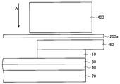
- the buffer material 200 a is installed on the second electronic component 60.
- the second electronic component 60 is finally pressure-bonded onto the anisotropic conductive film 10 by pressing the main pressure-bonding tool head 400 against the buffer material 200a.
- the pressurizing temperature and the applied pressure during the main pressure bonding vary depending on the material such as the anisotropic conductive film, but may be set within a range of, for example, 120 to 190 ° C. and 0.5 MPa or more and less than 2 MPa.
- the pressurization temperature and the applied pressure are preferably as low as possible within the above ranges.
- the applied pressure is preferably 0.5 MPa or more and 1 MPa or less.
- the pressing time is appropriately adjusted depending on the material of the anisotropic conductive film 10 and the like, but is set to a value at least that allows the anisotropic conductive film 10 to flow and cure.
- the anisotropic conductive film 10 is cured to become an anisotropic conductive layer 10a as shown in FIG. That is, the anisotropic conductive connection structure 1 is produced.
- the pressurizing force at the time of the main pressure bonding can be reduced, so that the deformation of the first electronic component 30 at the time of the main pressure bonding can be suppressed.
- the anisotropic conductive film 10 flows greatly even if the pressure applied during the main press bonding is low, so that the conductive particles more reliably differ between the first electronic component 30 and the second electronic component 60.
- An isotropic conductive connection can be made.
- the main crimping process itself may be performed by a conventional main crimping apparatus.
- the applied pressure at the anisotropic conductive connection that is, the applied pressure at the time of temporary press-bonding and the pressurized pressure at the time of final press-bonding are both less than 2 MPa. Damage to the electrode terminal group can be suppressed.
- FIG. 2 shows the structure of the anisotropic conductive connection structure 1 manufactured according to this embodiment.
- the anisotropic conductive connection structure 1 includes a first electronic component 30, an optical resin layer 40, a second electronic component 60, an anisotropic conductive layer 10a, and a third electronic component 70.
- the first electronic component 30 and the second electronic component 60 can be more reliably anisotropically connected while suppressing deformation of the first electronic component 30.
- the third electronic component 70 is a substrate of the image display device, the image display device includes the anisotropic conductive connection structure 1.
- anisotropic conductive films according to Test Examples 1 to 16 were produced by the following steps. That is, phenoxy resins YP-50 and YP-70 (all manufactured by Nippon Steel & Sumikin Chemical Co., Ltd.), polyester resins Byron 200, Byron 220, Byron 600, Byron 802 (all manufactured by Toyobo Co., Ltd.), bifunctional DCP (manufactured by Shin-Nakamura Chemical Co., Ltd.) as an acrylate monomer, M1600 (manufactured by Toagosei Co., Ltd.) as a urethane acrylate, SG80H (manufactured by Nagase ChemteX Corporation) as a rubber component, and P-1M as a phosphoric acid acrylate (Manufactured by Kyoeisha Chemical Industry Co., Ltd.), Perroyl L (manufactured by Kyoeisha Chemical Industry Co., Ltd.), Perroyl L (manufacture
- the particle size of the conductive particles was 10 ⁇ m.
- this coating solution was applied onto a release film so as to have a thickness of 18 ⁇ m after drying, and dried in an oven at 60 ° C. for 40 minutes.
- anisotropic conductive films according to Test Examples 1 to 16 were obtained.
- the number density of conductive particles contained in the anisotropic conductive films according to Test Examples 1 to 16 was determined by the following method. That is, the number density of conductive particles was determined by analyzing an image obtained by observing the anisotropic conductive film with a metal microscope using image analysis software WinROOF (manufactured by Mitani Corporation). . As a result, in any of the anisotropic conductive films, the number density was about 500 to 800 pieces / mm 2 .
- the minimum melt viscosity of the produced anisotropic conductive film was measured. First, a laminated sheet having a thickness of 300 ⁇ m was prepared by overlaying anisotropic conductive films. Next, the laminated sheet was set on a melt viscometer (manufactured by Thermo Fisher Scientific). Then, the minimum melt viscosity of the anisotropic conductive film was measured by driving the melt viscometer under the conditions of a temperature rising rate of 10 ° C./min, a frequency of 1 Hz, a pressure of 1 N, and a measurement temperature range of 30 to 180 ° C.
- the weight average molecular weight (Mw) was measured by gel permeation chromatography (GPC), and the glass transition point was measured by differential thermal scanning analysis (DSC).
- GPC gel permeation chromatography
- DSC differential thermal scanning analysis
- the weight average molecular weight (Mw) was calculated
- Measuring device Q100, manufactured by TA Instruments Inc.
- Measuring sample 5 mg (aluminum pan)
- Temperature rising rate The glass transition point was measured by heating at 10 ° C./min.
- ITO pattern glass was prepared as the first electronic component 30.
- a flexible substrate made of polyimide was prepared as the second electronic component.
- the thickness of the flexible substrate was 25 ⁇ m.
- an anisotropic conductive film was temporarily pressure-bonded on the first electronic component 30.
- the applied pressure at the time of pre-bonding was 1 MPa, the pressing temperature was 45 ° C., and the pressing time was 2 seconds.
- the release film was peeled off from the anisotropic conductive film, and the anisotropic conductive film and the second electronic component 60 were finally pressure bonded.
- the pressurizing force at the time of the main pressure bonding was set to the values shown in Tables 1 and 2, the pressurizing temperature was 130 ° C., and the pressurizing time was 10 seconds.
- connection resistance of the anisotropic conductive connection structure was measured with a digital multimeter (trade name: Digital Multimeter 7561, manufactured by Yokogawa Electric Corporation). When the connection resistance was 1 ⁇ or more, the connection resistance was evaluated as B (defect), and when it was less than 1 ⁇ , the connection resistance was evaluated as A (good).
- the anisotropic conductive films according to Test Examples 1 to 6 and 11 to 16 satisfy the requirements of this embodiment. For this reason, the connection resistance was good even when the applied pressure during the main pressure bonding was 0.5 MPa and 1 MPa. On the other hand, the anisotropic conductive films according to Test Examples 7 to 10 do not satisfy the requirements of this embodiment. For this reason, when the applied pressure at the time of the main pressure bonding is 1 MPa, the connection resistance is poor. On the other hand, when the applied pressure is 2 MPa, the connection resistance is good in all the test examples. However, when the first electronic component 30 is a plastic substrate, the first electronic component 30 is greatly deformed by this applied pressure. There is a possibility that.
- a plastic substrate (PET) was prepared as the first electronic component 30.
- Test Examples 1 to 6 the same test as in Test Examples 1 to 6 was conducted except that the conductive particles were changed to Au / Ni plating coated resin particles (average particle size 5 ⁇ m, manufactured by Nippon Chemical Industry Co., Ltd.) and L / S was 50/50. As a result, the same results as in Test Examples 1 to 6 were obtained.
- the same tests as in Test Examples 1 to 6 were conducted except that the conductive particles were changed to Au / Ni plating coated resin particles (average particle size 20 ⁇ m, manufactured by Nippon Chemical Industry Co., Ltd.) and L / S was changed to 300/300. However, the same results as in Test Examples 1 to 6 were obtained.
- the peel strength of the connection structure was measured in all the above test examples.
- the peel strength was measured using a tensile tester (trade name: Tensilon, manufactured by A & D). Specifically, after placing the connection structure cut to a width of 1 cm horizontally, the tensile strength (peel strength) at which the connection structure peeled when it was pulled at an angle of 90 degrees was measured. As a result, the peel strength was 6 N / cm or more in all the test examples. This is a value that causes no problem in practical use.
- Anisotropic conductive connection structure 10 Anisotropic conductive film (anisotropic conductive paste) 20 Release film 30 First electronic component 40 Optical resin layer 60 Second electronic component 70 Third electronic component
Landscapes
- Chemical & Material Sciences (AREA)
- Organic Chemistry (AREA)
- Engineering & Computer Science (AREA)
- Spectroscopy & Molecular Physics (AREA)
- Physics & Mathematics (AREA)
- Dispersion Chemistry (AREA)
- Microelectronics & Electronic Packaging (AREA)
- Chemical Kinetics & Catalysis (AREA)
- Manufacturing & Machinery (AREA)
- Adhesives Or Adhesive Processes (AREA)
- Conductive Materials (AREA)
- Electric Connection Of Electric Components To Printed Circuits (AREA)
- Adhesive Tapes (AREA)
- Wire Bonding (AREA)
- Non-Insulated Conductors (AREA)
Applications Claiming Priority (2)
| Application Number | Priority Date | Filing Date | Title |
|---|---|---|---|
| JP2017-026025 | 2017-02-15 | ||
| JP2017026025 | 2017-02-15 |
Publications (1)
| Publication Number | Publication Date |
|---|---|
| WO2018150897A1 true WO2018150897A1 (ja) | 2018-08-23 |
Family
ID=63169276
Family Applications (1)
| Application Number | Title | Priority Date | Filing Date |
|---|---|---|---|
| PCT/JP2018/003448 Ceased WO2018150897A1 (ja) | 2017-02-15 | 2018-02-01 | 異方性導電接続構造体、異方性導電接続構造体の製造方法、異方性導電フィルム、及び異方性導電ペースト |
Country Status (3)
| Country | Link |
|---|---|
| JP (1) | JP2018133331A (https=) |
| TW (1) | TW201834858A (https=) |
| WO (1) | WO2018150897A1 (https=) |
Cited By (1)
| Publication number | Priority date | Publication date | Assignee | Title |
|---|---|---|---|---|
| WO2025134747A1 (ja) * | 2023-12-22 | 2025-06-26 | 株式会社レゾナック | 回路接続用接着剤フィルム、接続構造体の製造方法、導電材料、及び接続構造体 |
Families Citing this family (1)
| Publication number | Priority date | Publication date | Assignee | Title |
|---|---|---|---|---|
| JP7510292B2 (ja) * | 2020-07-17 | 2024-07-03 | 京都エレックス株式会社 | 導電性接着剤組成物 |
Citations (7)
| Publication number | Priority date | Publication date | Assignee | Title |
|---|---|---|---|---|
| JP2000040542A (ja) * | 1998-07-23 | 2000-02-08 | Sharp Corp | 異方性導電膜およびそれを用いた電極接続構造 |
| JP2010199527A (ja) * | 2009-03-31 | 2010-09-09 | Sony Chemical & Information Device Corp | 接合体及びその製造方法 |
| JP2013055331A (ja) * | 2011-08-05 | 2013-03-21 | Sekisui Chem Co Ltd | 接続構造体の製造方法 |
| JP2014046622A (ja) * | 2012-08-31 | 2014-03-17 | Dexerials Corp | 透明導電体、入力装置および電子機器 |
| JP2014078479A (ja) * | 2012-09-24 | 2014-05-01 | Tamura Seisakusho Co Ltd | 異方性導電性ペーストおよびそれを用いたプリント配線基板 |
| JP2014102943A (ja) * | 2012-11-19 | 2014-06-05 | Dexerials Corp | 異方性導電フィルム、接続方法、及び接合体 |
| JP2016082070A (ja) * | 2014-10-16 | 2016-05-16 | デクセリアルズ株式会社 | 接続体の製造方法、電子部品の接続方法、接続体 |
Family Cites Families (6)
| Publication number | Priority date | Publication date | Assignee | Title |
|---|---|---|---|---|
| JPH11224976A (ja) * | 1998-02-05 | 1999-08-17 | Matsushita Electric Ind Co Ltd | 配線基板 |
| JP6024235B2 (ja) * | 2011-08-30 | 2016-11-09 | 日立化成株式会社 | 接着剤組成物及び回路接続構造体 |
| JP2013199525A (ja) * | 2012-03-23 | 2013-10-03 | Dic Corp | 共重合ポリエステル樹脂及び樹脂組成物 |
| KR20150059376A (ko) * | 2013-11-22 | 2015-06-01 | 삼성전기주식회사 | 터치센서 모듈 및 그 제조 방법 |
| JP2016072097A (ja) * | 2014-09-30 | 2016-05-09 | デクセリアルズ株式会社 | 接続方法、接合体、及びタッチパネル装置 |
| JP2016170330A (ja) * | 2015-03-13 | 2016-09-23 | 富士ゼロックス株式会社 | 画像形成方法、画像形成装置、液体現像剤カートリッジ、及び液体現像剤 |
-
2018
- 2018-02-01 JP JP2018016466A patent/JP2018133331A/ja active Pending
- 2018-02-01 WO PCT/JP2018/003448 patent/WO2018150897A1/ja not_active Ceased
- 2018-02-09 TW TW107104672A patent/TW201834858A/zh unknown
Patent Citations (7)
| Publication number | Priority date | Publication date | Assignee | Title |
|---|---|---|---|---|
| JP2000040542A (ja) * | 1998-07-23 | 2000-02-08 | Sharp Corp | 異方性導電膜およびそれを用いた電極接続構造 |
| JP2010199527A (ja) * | 2009-03-31 | 2010-09-09 | Sony Chemical & Information Device Corp | 接合体及びその製造方法 |
| JP2013055331A (ja) * | 2011-08-05 | 2013-03-21 | Sekisui Chem Co Ltd | 接続構造体の製造方法 |
| JP2014046622A (ja) * | 2012-08-31 | 2014-03-17 | Dexerials Corp | 透明導電体、入力装置および電子機器 |
| JP2014078479A (ja) * | 2012-09-24 | 2014-05-01 | Tamura Seisakusho Co Ltd | 異方性導電性ペーストおよびそれを用いたプリント配線基板 |
| JP2014102943A (ja) * | 2012-11-19 | 2014-06-05 | Dexerials Corp | 異方性導電フィルム、接続方法、及び接合体 |
| JP2016082070A (ja) * | 2014-10-16 | 2016-05-16 | デクセリアルズ株式会社 | 接続体の製造方法、電子部品の接続方法、接続体 |
Cited By (1)
| Publication number | Priority date | Publication date | Assignee | Title |
|---|---|---|---|---|
| WO2025134747A1 (ja) * | 2023-12-22 | 2025-06-26 | 株式会社レゾナック | 回路接続用接着剤フィルム、接続構造体の製造方法、導電材料、及び接続構造体 |
Also Published As
| Publication number | Publication date |
|---|---|
| JP2018133331A (ja) | 2018-08-23 |
| TW201834858A (zh) | 2018-10-01 |
Similar Documents
| Publication | Publication Date | Title |
|---|---|---|
| CN103069656B (zh) | 各向异性导电膜、接合体的制造方法以及接合体 | |
| JP5690637B2 (ja) | 異方性導電フィルム、接続方法及び接続構造体 | |
| KR101886909B1 (ko) | 이방성 도전 접속 재료, 접속 구조체, 접속 구조체의 제조 방법 및 접속 방법 | |
| JP5509542B2 (ja) | 配線部材の接続構造体及び配線部材の接続方法 | |
| KR101344965B1 (ko) | 이방성 도전 필름, 접합체, 및 접합체의 제조 방법 | |
| KR20140064651A (ko) | 이방성 도전 필름, 접속 방법, 및 접합체 | |
| CN107432084A (zh) | 各向异性导电连接结构体、各向异性导电连接方法和各向异性导电粘接剂 | |
| JP6505423B2 (ja) | 実装体の製造方法、及び異方性導電フィルム | |
| WO2011152421A1 (ja) | 異方性導電膜及びその製造方法 | |
| JP5816456B2 (ja) | 異方性導電接続材料、フィルム積層体、接続方法及び接続構造体 | |
| JP5654289B2 (ja) | 実装体の製造方法及び実装体並びに異方性導電膜 | |
| WO2018150897A1 (ja) | 異方性導電接続構造体、異方性導電接続構造体の製造方法、異方性導電フィルム、及び異方性導電ペースト | |
| JP2010251336A (ja) | 異方性導電フィルム及びこれを用いた接続構造体の製造方法 | |
| JP2016173982A (ja) | 異方性導電フィルム | |
| JP6639079B2 (ja) | 異方性導電材料 | |
| JP6654954B2 (ja) | 異方性導電接続構造体 | |
| KR102524175B1 (ko) | 접속 구조체의 제조 방법 및 접속 필름 | |
| WO2020071271A1 (ja) | 異方性導電フィルム、接続構造体、接続構造体の製造方法 | |
| JP6431572B2 (ja) | 接続フィルム、接続フィルムの製造方法、接続構造体、接続構造体の製造方法及び接続方法 | |
| JP5966069B2 (ja) | 異方性導電フィルム、接合体及び接続方法 | |
| JP6177642B2 (ja) | 接続フィルム、接続構造体、接続構造体の製造方法、接続方法 | |
| JP5924896B2 (ja) | 接合体の製造方法 | |
| JP2018093055A (ja) | 異方性導電フィルムの仮圧着方法、異方性導電フィルムの仮圧着装置、および異方性導電接続構造体 | |
| HK1189389B (en) | Anisotropic conductive connection material, film laminate, connection method, and connection structure |
Legal Events
| Date | Code | Title | Description |
|---|---|---|---|
| 121 | Ep: the epo has been informed by wipo that ep was designated in this application |
Ref document number: 18754796 Country of ref document: EP Kind code of ref document: A1 |
|
| DPE1 | Request for preliminary examination filed after expiration of 19th month from priority date (pct application filed from 20040101) | ||
| NENP | Non-entry into the national phase |
Ref country code: DE |
|
| 122 | Ep: pct application non-entry in european phase |
Ref document number: 18754796 Country of ref document: EP Kind code of ref document: A1 |