WO2018139196A1 - プロセッサ、情報処理装置及びプロセッサの動作方法 - Google Patents
プロセッサ、情報処理装置及びプロセッサの動作方法 Download PDFInfo
- Publication number
- WO2018139196A1 WO2018139196A1 PCT/JP2018/000279 JP2018000279W WO2018139196A1 WO 2018139196 A1 WO2018139196 A1 WO 2018139196A1 JP 2018000279 W JP2018000279 W JP 2018000279W WO 2018139196 A1 WO2018139196 A1 WO 2018139196A1
- Authority
- WO
- WIPO (PCT)
- Prior art keywords
- adder
- input
- circuit
- data
- registers
- Prior art date
- Legal status (The legal status is an assumption and is not a legal conclusion. Google has not performed a legal analysis and makes no representation as to the accuracy of the status listed.)
- Ceased
Links
Images








Classifications
-
- G—PHYSICS
- G06—COMPUTING OR CALCULATING; COUNTING
- G06N—COMPUTING ARRANGEMENTS BASED ON SPECIFIC COMPUTATIONAL MODELS
- G06N3/00—Computing arrangements based on biological models
- G06N3/02—Neural networks
- G06N3/06—Physical realisation, i.e. hardware implementation of neural networks, neurons or parts of neurons
- G06N3/063—Physical realisation, i.e. hardware implementation of neural networks, neurons or parts of neurons using electronic means
-
- G—PHYSICS
- G06—COMPUTING OR CALCULATING; COUNTING
- G06F—ELECTRIC DIGITAL DATA PROCESSING
- G06F7/00—Methods or arrangements for processing data by operating upon the order or content of the data handled
- G06F7/38—Methods or arrangements for performing computations using exclusively denominational number representation, e.g. using binary, ternary, decimal representation
- G06F7/48—Methods or arrangements for performing computations using exclusively denominational number representation, e.g. using binary, ternary, decimal representation using non-contact-making devices, e.g. tube, solid state device; using unspecified devices
- G06F7/483—Computations with numbers represented by a non-linear combination of denominational numbers, e.g. rational numbers, logarithmic number system or floating-point numbers
- G06F7/487—Multiplying; Dividing
- G06F7/4876—Multiplying
-
- G—PHYSICS
- G06—COMPUTING OR CALCULATING; COUNTING
- G06F—ELECTRIC DIGITAL DATA PROCESSING
- G06F15/00—Digital computers in general; Data processing equipment in general
- G06F15/76—Architectures of general purpose stored program computers
- G06F15/80—Architectures of general purpose stored program computers comprising an array of processing units with common control, e.g. single instruction multiple data processors
-
- G—PHYSICS
- G06—COMPUTING OR CALCULATING; COUNTING
- G06F—ELECTRIC DIGITAL DATA PROCESSING
- G06F17/00—Digital computing or data processing equipment or methods, specially adapted for specific functions
- G06F17/10—Complex mathematical operations
- G06F17/15—Correlation function computation including computation of convolution operations
- G06F17/153—Multidimensional correlation or convolution
-
- G—PHYSICS
- G06—COMPUTING OR CALCULATING; COUNTING
- G06F—ELECTRIC DIGITAL DATA PROCESSING
- G06F17/00—Digital computing or data processing equipment or methods, specially adapted for specific functions
- G06F17/10—Complex mathematical operations
- G06F17/16—Matrix or vector computation, e.g. matrix-matrix or matrix-vector multiplication, matrix factorization
-
- G—PHYSICS
- G06—COMPUTING OR CALCULATING; COUNTING
- G06F—ELECTRIC DIGITAL DATA PROCESSING
- G06F7/00—Methods or arrangements for processing data by operating upon the order or content of the data handled
- G06F7/38—Methods or arrangements for performing computations using exclusively denominational number representation, e.g. using binary, ternary, decimal representation
- G06F7/48—Methods or arrangements for performing computations using exclusively denominational number representation, e.g. using binary, ternary, decimal representation using non-contact-making devices, e.g. tube, solid state device; using unspecified devices
- G06F7/483—Computations with numbers represented by a non-linear combination of denominational numbers, e.g. rational numbers, logarithmic number system or floating-point numbers
- G06F7/485—Adding; Subtracting
-
- G—PHYSICS
- G06—COMPUTING OR CALCULATING; COUNTING
- G06F—ELECTRIC DIGITAL DATA PROCESSING
- G06F7/00—Methods or arrangements for processing data by operating upon the order or content of the data handled
- G06F7/38—Methods or arrangements for performing computations using exclusively denominational number representation, e.g. using binary, ternary, decimal representation
- G06F7/48—Methods or arrangements for performing computations using exclusively denominational number representation, e.g. using binary, ternary, decimal representation using non-contact-making devices, e.g. tube, solid state device; using unspecified devices
- G06F7/544—Methods or arrangements for performing computations using exclusively denominational number representation, e.g. using binary, ternary, decimal representation using non-contact-making devices, e.g. tube, solid state device; using unspecified devices for evaluating functions by calculation
- G06F7/5443—Sum of products
-
- G—PHYSICS
- G06—COMPUTING OR CALCULATING; COUNTING
- G06F—ELECTRIC DIGITAL DATA PROCESSING
- G06F9/00—Arrangements for program control, e.g. control units
- G06F9/06—Arrangements for program control, e.g. control units using stored programs, i.e. using an internal store of processing equipment to receive or retain programs
- G06F9/30—Arrangements for executing machine instructions, e.g. instruction decode
- G06F9/38—Concurrent instruction execution, e.g. pipeline or look ahead
-
- G—PHYSICS
- G06—COMPUTING OR CALCULATING; COUNTING
- G06N—COMPUTING ARRANGEMENTS BASED ON SPECIFIC COMPUTATIONAL MODELS
- G06N3/00—Computing arrangements based on biological models
- G06N3/02—Neural networks
- G06N3/04—Architecture, e.g. interconnection topology
- G06N3/045—Combinations of networks
-
- G—PHYSICS
- G06—COMPUTING OR CALCULATING; COUNTING
- G06N—COMPUTING ARRANGEMENTS BASED ON SPECIFIC COMPUTATIONAL MODELS
- G06N3/00—Computing arrangements based on biological models
- G06N3/02—Neural networks
- G06N3/04—Architecture, e.g. interconnection topology
- G06N3/0464—Convolutional networks [CNN, ConvNet]
-
- G—PHYSICS
- G06—COMPUTING OR CALCULATING; COUNTING
- G06T—IMAGE DATA PROCESSING OR GENERATION, IN GENERAL
- G06T1/00—General purpose image data processing
- G06T1/20—Processor architectures; Processor configuration, e.g. pipelining
-
- G—PHYSICS
- G06—COMPUTING OR CALCULATING; COUNTING
- G06F—ELECTRIC DIGITAL DATA PROCESSING
- G06F9/00—Arrangements for program control, e.g. control units
- G06F9/06—Arrangements for program control, e.g. control units using stored programs, i.e. using an internal store of processing equipment to receive or retain programs
- G06F9/30—Arrangements for executing machine instructions, e.g. instruction decode
- G06F9/30003—Arrangements for executing specific machine instructions
- G06F9/30007—Arrangements for executing specific machine instructions to perform operations on data operands
- G06F9/3001—Arithmetic instructions
Definitions
- the present invention relates to a processor, an information processing apparatus, and an operation method of the processor.
- Deep learning (DL1: Deep Learning) is executed by arithmetic processing of a processor in the information processing apparatus.
- DL is a general term for algorithms that use deep neural networks (DNNs).
- DNNs deep neural networks
- a convolutional neural network (CNN) is often used in DNN.
- the CNN is widely used as a DNN for determining the characteristics of image data, for example.
- the CNN that determines the characteristics of the image data receives the image data, performs a convolution operation using a filter, and detects the characteristics of the image data (for example, edge characteristics).
- the CNN convolution operation is performed by, for example, a processor.
- Patent Document 1 below discloses a memory data format and an execution performance of an arithmetic unit.
- the above convolution calculation is performed by moving the position of the coefficient filter in the image data in the raster scan direction of the image data, and the pixel data of the neighboring matrix centered on the target pixel of the image data and the coefficient (weight) of the coefficient filter. Repeat the product-sum operation.
- the size of the coefficient filter is generally an odd square (a value obtained by adding 1 to a multiple of 8). For example, 3 ⁇ 3, 5 ⁇ 5, 7 ⁇ 7, 9 ⁇ 9, 11 ⁇ 11, and the like.
- the convolution operation is a repetition of the product-sum operation, and it is desirable to perform parallel processing by a plurality of product-sum operation units.
- DNN image data for multiple channels (pixel data for multiple planes)
- a processor generally has a power-of-two arithmetic unit. Therefore, for example, if nine coefficients and pixel data in the case of a 3 ⁇ 3 coefficient filter are input to 16 arithmetic units, some arithmetic units may not be able to process the product-sum operation. It is not possible to operate the individual arithmetic units efficiently.
- transposing image data and inputting a plurality of sets of pixel data and their coefficients in parallel to 16 arithmetic units In that case, a process for transposing the image data is required, and the arithmetic unit needs to stop operating during the transposition process. Therefore, the 16 arithmetic units cannot be operated efficiently.
- an object of one embodiment is to provide a processor, an information processing apparatus, and an operation method of a processor that efficiently perform operations.
- One embodiment is: Multiple processor cores, An internal memory accessed from the plurality of processor cores,
- the arithmetic unit included in any of the plurality of processor cores is A plurality of first registers provided in the first stage;
- a normal adder circuit comprising: a first adder for adding a plurality of outputs of the plurality of first registers; and a second register provided in a second stage for latching the output of the first adder;
- An overtaking circuit having a second adder for adding a plurality of outputs of the plurality of first registers;
- a synthesis circuit having a third adder for adding the output of the normal adder circuit and the output of the overtaking adder circuit, and a third register provided in a third stage for latching the output of the second adder
- the first adder and the second adder select and input a plurality of outputs of the plurality of first registers mutually exclusive, and the first, second, and third registers are clocks
- a processor having an adder circuit that latch
- the calculation can be performed efficiently.
- AOS ArrayOf
- FIG. 10 is a diagram showing a first example of a generation procedure of input neighborhood matrix image data to be input to a product-sum calculator.
- FIG. 10 is a diagram showing a first example of a generation procedure of input neighborhood matrix image data to be input to a product-sum calculator. It is a figure which shows the structure of the product sum arithmetic unit with an overtaking route of this Embodiment. It is a sequence diagram which shows the operation
- FIG. 10 is a sequence diagram showing selection and non-selection states of masks Mb0-7 and Mc0-7 in the case of a 3 ⁇ 3 filter.
- FIG. 14 is a sequence diagram showing an operation of the product-sum operation unit in FIG. It is a sequence diagram which shows operation
- FIG. 1 is a diagram showing a configuration of an information processing apparatus (deep learning server) that performs deep learning in the present embodiment.
- the server 1 can communicate with the sensing device group 30 and the terminal device 32 via a network.
- the sensing device group 30, for example, captures an image with an image sensor to generate image data, and transmits the image data to the server 1.
- the terminal device 32 receives the determination result of the feature of the image data from the server 1 and outputs it.
- the server 1 includes a CPU (Central Processing Unit) 10 that is a general-purpose processor and a GPU (Graphic Processing Unit) 11 that is a graphic processor.
- the server 1 further includes a main memory 12 such as a DRAM, a network interface 14 such as a NIC (Network Interface Card), a large-capacity auxiliary memory 20 such as a hard disk or an SSD (Solid Storage Device), and a bus BUS connecting them. And have.
- the auxiliary memory 20 stores a deep learning calculation program 22, a deep learning parameter 24, and the like.
- the auxiliary memory 20 stores an operating system (OS) (not shown), various middleware programs, and the like.
- OS operating system
- the processor 10 and the graphic processor 11 develop the above programs and parameters in the main memory 12, and execute the programs based on the parameters.
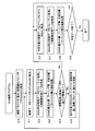
- FIG. 2 is a flowchart showing a schematic process of the deep learning calculation program.
- the DL calculation program is a program that executes, for example, DNN calculation.
- the processors 10 and 11 execute the DL operation program and execute the processing in the learning mode and the determination mode.
- a DLN that determines the characteristics of image data will be described as an example of DL.
- the processors 10 and 11 read the initial values of the operation parameters (filter coefficients (weights) and the like) from the main memory 12 and write them into the high-speed memory SRAM in the processor 11 (S10). Further, the processor reads the image data transmitted from the sensing device group 30 from the main memory 12 and writes it in the high-speed memory SRAM (S11). The processor then converts the format of the image data to generate neighborhood matrix image data (arithmetic processing data) for computing unit input (S12), DNN convolution layer, pooling layer, fully connected layer, softmax layer ( Output layer) processing is performed (S13). This calculation is performed for each of a predetermined number of image data. The calculation result is, for example, that the image data is one of the numbers 0 to 1.
- the processors 10 and 11 determine whether or not the difference between the calculation result and the teacher data that is the correct data of the image data is equal to or less than a threshold (S14). If the difference is not equal to or less than the threshold (NO in S14), the calculation parameter is set. Based on the difference, the backward calculation of DNN is executed and the calculation parameter is updated (S15). Then, the above steps S11-S13 are repeated with the updated calculation parameters.
- the difference between the calculation result and the teacher data is, for example, 1000 calculation results calculated with respect to 1000 pieces of image data, and a total value of differences between the 1000 pieces of teacher data.
- the processors 10 and 11 read the determination target image data from the main memory (S16), convert the format of the image data to generate neighborhood matrix image data for computing unit input (S17), Computation processing is performed on the embedded layer, the pooling layer, the fully connected layer, and the softmax layer (S18). The processors 10 and 11 repeat the above determination processing until the image data to be determined is completed (S19). The determination result is transmitted to the terminal device 32 and output.
- FIG. 3 is a diagram showing the configuration of the graphic processor (GPU) 11 and the configuration of the core CORE in the GPU.
- the GPU 11 can access the main memory M_MEM.
- the GPU includes, for example, eight processor cores CORE, a plurality of high-speed memory SRAMs arranged corresponding to the respective processor cores CORE, an internal bus I_BUS, and a memory controller MC that controls access to the main memory M_MEM. Have.
- the GPU includes an L1 cache memory in each core CORE, an L2 cache memory shared by the eight cores CORE, and various peripheral resource circuits, which are not shown in FIG.
- the GPU further includes a direct memory access control circuit DMA that controls data transfer between internal high-speed memory SRAMs, data transfer between the main memory M_MEM and the high-speed memory SRAM, and the like.
- DMA direct memory access control circuit
- each processor core CORE like a normal processor core, has an instruction fetch circuit FETCH that acquires instructions from memory, a decoder DEC that decodes the acquired instructions, and a plurality of operations that calculate instructions based on the decoding results And an ALU and its register group REG, and a memory access control circuit MAC for accessing the high-speed memory SRAM.
- FETCH instruction fetch circuit
- DEC decoder
- MAC memory access control circuit
- the GPU is realized by a semiconductor chip, for example, and is a DL device according to the present embodiment.
- the GPU reads out the image data from the main memory M_MEM that stores the image data transmitted from the above-described sensing device group, and writes it in the internal high-speed memory SRAM. Then, the arithmetic unit ALU in each core CORE inputs the image data written in the SRAM, executes the arithmetic processing of each layer of the DNN, and generates the output of the DNN.
- FIG. 4 is a diagram showing an example of CNN.
- the CNN that performs image data determination processing includes an input layer INPUT_L to which image data IM_D that is input data is input, a plurality of convolution layers CNV_L and a pooling layer PL_L, a total coupling layer C_L, and a softmax layer ( Output layer) OUT_L.
- the convolution layer CNV_L generates image data F_IM_D having a feature amount by filtering the image data IM_D with the coefficient filter FLT.
- image data F_IM_D of each feature amount is generated.
- the pooling layer PL_L selects a representative value (for example, a maximum value) of the node values of the convolution layer.
- the output layer OUT_L includes, for example, the determination result (0 of the number in the image data). ⁇ 9) is output.
- the convolution layer CNV_L includes, for example, pixel data of a 3 ⁇ 3 neighborhood matrix of image data IM_D having pixel data of an M ⁇ N two-dimensional pixel matrix, and coefficient data of a 3 ⁇ 3 coefficient filter FLT that is the same as the neighborhood matrix. And multiplying and adding the multiplication results, the pixel data F_IM_D of the pixel of interest at the center of the neighborhood matrix is generated. This filtering process is performed on all the pixels of the image data IM_D while shifting the coefficient filter in the raster scan direction of the image data IM_D. This is a convolution operation.
- FIG. 5 is a diagram for explaining the convolution operation.
- FIG. 5 shows, for example, input image data IN_DATA with padding P added around image data of 5 rows and 5 columns, a coefficient filter FLT0 having weights W0 to W8 of 3 rows and 3 columns, and an output image that has been subjected to a convolution operation.
- Data OUT_DATA is indicated.
- the convolution operation is a product-sum operation in which a plurality of pixel data in the neighborhood matrix centered on the target pixel and a plurality of coefficients (weights) W0 to W8 of the coefficient filter FLT0 are multiplied and added, and the coefficient filter FLT0 is converted into image data. This operation is repeated while shifting in the raster scan direction.
- the product-sum operation expression is as follows.
- Xi ⁇ (Xi * Wi) (1)
- Xi on the right side is pixel data of the input image IN_DATA
- Wi is a coefficient
- Xi on the left side is a product-sum operation value
- pixel data of the output image OUT_DATA is there.
- FIG. 6 is a diagram illustrating an example in which an array of data structures (AOS: ArrayOf Structure) stored in the memory is input to 16 arithmetic units.
- AOS ArrayOf Structure
- input data IN_DATA includes 16 words of input image data IN_DATA in each row in an array of structure (AOS) format and a coefficient FLT (W0-W8) of 16 words in 16 arithmetic units ALU in the row order. This is an example of input.
- pixel data a0-a8, b0-b8, c0-c8, d0-d8 are packed in the first nine words of each row, and pixel data of the value “0” is packed in the remaining seven words.
- the coefficient filter FLT also has coefficient data W0-W8 in the first 9 words and the value “0” in the remaining 7 words. "Packed. Each pair of pixel data and coefficient data in the corresponding column is input to 16 inputs of the arithmetic unit ALU.
- FIG. 7 is a diagram illustrating an example in which data of a structure of array (SOA) obtained by transposing AOS, which is an array of data structures stored in a memory, is input to four arithmetic units.
- the input data IN_DATA and the coefficient data W0-W8 of the coefficient filter FLT are the same as in FIG.
- Transposed data TRSP_DATA in which the column direction and the row direction of the input data IN_DATA are reversed by transposition processing is input to the four arithmetic units ALU in pairs with coefficient data.
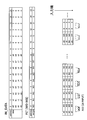
- FIG. 8 is a diagram showing the configuration of the input data of the arithmetic unit in the present embodiment in comparison with the examples of FIGS.
- the configurations AOS and SOA of the input data shown in FIGS. 6 and 7 are shown in FIGS. 8B and 8C.
- FIG. 8 only the input data IN_DATA is shown as the data input to the computing unit for the sake of simplicity, and the filter coefficients are omitted.
- FIG. 8B is different from FIG. 6 in that 16 inputs of the arithmetic unit ALU are arranged in the vertical direction on the right side
- FIG. 8C is different from FIG. 7 in that 16 arithmetic units ALU are in the vertical direction on the right side.
- (B) since the format of the input data is AOS, the arithmetic unit ALU having 7 inputs out of 16 inputs is not operating.
- (C) since the format of the input data is SOA, the 16 arithmetic units ALU operate at full capacity, but transposition processing is required for formatting into SOA, and processing is not performed until the computation starts. The operation of the cycle calculator stops.
- FIG. 8A shows a configuration of input data and four arithmetic units in this embodiment.
- nine pixel data a0 to a8 are input to the eight inputs of the arithmetic unit ALU with an 8-word width. Therefore, the first 8-word input includes 8 pixel data a0-a7, and the next 8-word input includes the remaining pixel data a8 together with a part b0-b6 of the next 9 pixel data. It is.
- the arithmetic unit ALU in the present embodiment inputs a number of input data exceeding the number of inputs in a plurality of cycles, and outputs the operation results of all input data after the number of operation cycles of the data input in the first cycle.
- the computing unit performs pipeline processing at a plurality of stages and outputs a computation result.
- the arithmetic unit in the present embodiment has an overtaking processing route having a smaller number of stages than usual in addition to a normal pipeline processing route. Then, the calculation of the input data that did not fit in the first 8-word input is executed in the overtaking process route, and the calculation result of all the input data is output after the number of calculation cycles of the data input in the first cycle.
- FIG. 9 is a diagram showing the configuration of the graphic processor GPU (DL device) in the present embodiment.
- the GPU of FIG. 9 shows a configuration obtained by simplifying the configuration of FIG.
- the GPU is a DL chip (DL device) that performs DL operations.
- the GPU includes a processor core CORE, internal high-speed memories SRAM_0 and SRAM_1, an internal bus I_BUS, a memory controller MC, an image data format converter FMT_C, and a control bus C_BUS.
- the format converter FMT_C converts the format of the image data input from the main memory M_MEM into input neighborhood matrix image data for input to the arithmetic unit in the core CORE.
- the format converter FMT_C is a high-speed memory SRAM_0, DMA that performs data transfer between SRAM_1. That is, the DMA has a format converter in addition to the original data transfer circuit. However, the format converter may be configured separately from the DMA. Then, the DMA inputs the image data of the high-speed memory SRAM_0, and writes the neighborhood matrix image data generated by the format conversion to another high-speed memory SRAM_1.
- Processor core CORE has a product-sum calculator.
- the product-sum calculator multiplies the neighborhood matrix image data generated by the format converter and the coefficient data of the coefficient filter and adds them.
- FIG. 10 is a diagram illustrating a configuration of the format converter FMT_C.
- the format converter FMT_C includes a control bus interface C_BUS_IF of the control bus C_BUS, a control data register CNT_REG for storing control data, and a control circuit CNT such as a state machine. Control data is transferred from the core (not shown) to the control bus C_BUS, and the control data is stored in the control register.
- the control circuit CNT controls transfer of image data from the first high-speed memory SRAM_0 to the second high-speed memory SRAM_1.
- the control circuit CNT controls the setting of parameter values in the parameter register 42 and the start and end of format conversion in addition to the transfer control of the image data. That is, the control circuit CNT reads the image data from the first high-speed memory SRAM_0, converts the format, and writes it to the second high-speed memory SRAM_1.
- the control circuit CNT performs format conversion during data transfer of image data. When the data transfer is performed, the control circuit designates the address of the image data and accesses the high speed memory SRAM. Then, the control circuit sets a parameter value of a register necessary for format conversion corresponding to the address of the image data.
- the format converter FMT_C further includes a first DMA memory DMA_M0, a second DMA memory DMA_M1, and a format conversion circuit 40 and a concatenation (coupling circuit) 44 between these memories.
- a plurality of sets of the format conversion circuit 40 and the combination circuit 44 are provided, and the format conversion of the plurality of sets of neighboring matrix image data is performed in parallel.
- a coupling circuit parameter register 42 for setting a coupling circuit parameter is provided.
- a transposition circuit TRSP that transposes image data and a data bus interface D_BUS_IF connected to the data bus D_BUS of the internal bus I_BUS are provided.
- the core CORE incorporating the arithmetic unit ALU reads the format-converted neighborhood matrix image data stored in the second high-speed memory SRAM_1, and the built-in sum-of-products arithmetic unit performs the convolution operation.
- the feature amount data is written to the high-speed memory again.
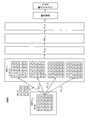
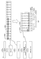
- FIG. 11 and FIG. 12 are diagrams showing a first example of a procedure for generating image data of an input neighborhood matrix to be input to a product-sum calculator.
- the main memory M_MEM stores image data IM_DATA of 13 rows and 13 columns with a width of 1 row and 32 words.
- the image data IM_DATA in 13 rows and 13 columns has pixel data X0 to X168 of 169 words.
- the memory controller MC in the GPU reads the image data IM_DATA in the main memory M_MEM via a 32-word external bus, converts the 32-word width to 16-word width, and passes the 16-word internal bus I_BUS. To write to the first high-speed memory SRAM_0. This data transfer is performed by, for example, a standard data transfer function of DMA.
- the DMA which is a format converter, reads the image data in the first high-speed memory SRAM_0 via the internal bus I_BUS and writes it to the first DMA memory DMA_M0. Then, the data format conversion circuit 40 extracts the 9-pixel data of the neighborhood matrix from the image data data0 in the first DMA memory, and generates 16-word data data1.
- the combining circuit CONC has eight sets of neighborhood matrix image data data2 Each set of 9-word pixel data is packed in the second DMA memory DMA_M1 of 16 words in one row in the raster scan direction.
- the first set of neighborhood matrix image data a0-a8 is stored across the first and second rows of the second DMA memory
- the second set of neighborhood matrix image data b0-b8 is stored in the second row.
- control circuit CNT transfers the image data data2 packed with the neighborhood matrix image data in the second DMA memory DMA_M1 to the second high-speed memory SRAM_1 via the internal bus without performing transposition processing.
- the core CORE in the GPU reads the neighborhood matrix image data data3 in the second high-speed memory SRAM_1 by 16 words, converts the 16 words into 8 words, and generates data data3. Then, the neighborhood matrix image data is input together with the coefficient (W0-W8) in units of 8 words to the 8 multipliers MLTP in the first stage of the single product-sum calculator SoP provided in the core CORE. As a result, the product-sum operation unit SoP multiplies the coefficient by 8 words in the pixel data of the 9-word neighborhood matrix, adds the multiplication results, and outputs the product-sum operation result. Multiply-accumulator SoP For the remaining pixel data in the second row (eg, a8 in the figure), the multiplication value with the coefficient is added to the product sum value of the eight words in the first row by an overtaking circuit (not shown).
- the product-sum operation unit SoP in the core CORE inputs the neighborhood matrix image data in the second DMA memory DMA_M1 subjected to the format conversion without being transposed, so there is no cycle to wait until the calculation starts.
- the operating rate of the computing unit can be increased.
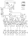
- FIG. 13 is a diagram illustrating a configuration of a product-sum operation unit with an overtaking route according to the present embodiment.
- 13 has pipeline stages ST0 to ST5, each pipeline stage has a plurality or a single register RG, a clock (not shown) is supplied to each stage register RG, and the clock input The input data is latched in response to.
- the input stage ST0 includes eight pairs of registers RG00-03 and RG04-07 that latch pixel data X0-X7 and coefficients W0-W7, respectively.
- Eight multipliers MP0-3 and MP4-7 in the stage ST1 multiply the pixel data X0-X7 latched in the eight pairs of registers in the input stage and the coefficients W0-W7, respectively.
- the eight registers RG10-13 and RG14-17 in the stage ST1 latch the multiplied values of the eight multipliers, respectively.
- stage ST2 includes an adder AD20 that adds multiplication values X0 * W0 and X1 * W1, an adder AD21 that adds multiplication values X2 * W2 and X3 * W3, and multiplication values X4 * W4 and X5 * W5.
- An adder AD22 for adding and an adder AD23 for adding the multiplication values X6 * W6 and X7 * W7 are provided.
- the four registers RG20-RG23 in stage ST2 These added values are latched respectively.
- each of the four adders AD20-23 has masks Mb0-3 and Mb4-7 that pass or do not pass (non-mask or mask) the input signal by the control signal CNT at a pair of input terminals. That is, the mask Mb0-7 is an AND gate that inputs each output of the register RG10-17 and the control signal CNT.
- the input of the normal route adder AD20-23 is validated.
- the control signals of the masks Mb0-3 and Mb4-7 are set to “0” (non-passing)
- the input of the normal route adder AD20-23 is invalidated and the input value “0” is input.
- the product-sum operation unit includes a setting register 50 in which parameters are set from a control core (not shown), and a control state machine 52 that outputs the control signal CNT based on the set parameters.
- a control state machine 52 sets all the control signals CNT of the masks Mb0-3 and Mb4-7 to “1” (passed)
- the input of the adder AD20-23 of the normal route is enabled and the clock of the normal route is set.
- the four registers RG20 to RG23 of the stage ST2 latch the added values of the four adders AD20-23.
- the stage ST3 includes adders AD30, AD31 and AD32, AD33, and two registers RG30 and RG31 that latch the outputs of the adders AD31 and AD33, respectively.
- the stage ST4 has an adder AD40 and a register RG40.
- the stage ST5 constitutes an accumulator ACML that accumulates the product-sum addition values of the eight sets of image data X0-X7 and coefficients W0-W7 latched by the register RG40 in synchronization with the clock.
- the initial value IV of the accumulator is “0”, and the adder AD50 adds the product-sum value of the register RG40 to the input value selected by the selector Sa0, and the register RG50 latches the added value. That is, accumulator ACML cumulatively adds the product-sum values of register RG40.
- the output of the register RG50 is the result RESULT of the product-sum adder.
- the adders AD20 and AD21, the registers RG20 and RG21, and the adder AD30 constitute a first normal adder circuit RGL_0 having a normal route. Further, the adders AD22 and AD23, the registers RG22 and RG23, and the adder AD32 constitute a second normal addition circuit RGL_1 having a normal route.
- the configurations from the registers RG10-13 and RG14-17 of the stage ST1 to the adders AD30 and AD32 respectively constitute the normal adders RGL_0 and RGL_1.
- the control state machine 52 sets the control signal CNT of the mask Mb0-3 and Mb4-7 of the normal route circuit to “1”, and in 8 clock cycles, 8 sets of input image data X0-X7 and coefficient W0 ⁇
- the product-sum value of each of W7 is output from register RG40.
- the control state machine 52 selects the selector Sa0 on the initial value IV side, resets the register RG in the accumulator ACML, sets the selector Sa0 to the selection on the register RG50 side, and outputs the product sum as the output of the register RG40. Cumulatively add values.
- the first overtaking circuit OVTK_0 adds four sets of multiplication values X0 * W0, X1 * W1, X2 * W2, and X3 * W3 latched by the four registers RG10-13 of the stage ST1, O_AD20, 21, It has O_AD30.
- the second overtaking circuit OVTK_1 adds four sets of multiplication values X4 * W4, X5 * W5, X6 * W6, and X7 * W7 latched by the four registers RG14-17 of the stage ST1. , 23 and O_AD31.
- the adders O_AD 20, 21, 22, and 23 have the masks Mc 0-3 and Mc 4-7 described above at each pair of input terminals, and “1” “0” of the control signal CNT from the control state machine 52. , The inputs of the respective masks Mc0-3 and Mc4-7 are controlled to be selected (passed) and not selected (not passed). When not selected, the input value is “0”.
- the overtaking circuit allows the multiplication value (RG10-13, RG14-17) delayed by 1 cycle in stage ST1 to catch up with the addition value (AD30, AD32) in the previous cycle in stage ST3. It is added to the added value of the previous cycle by AD31 and AD33.
- the adding circuit from the register RG10-13 to the register RG30 having the overtaking circuit OVTK_0 in FIG. 13 is the minimum unit of the adding circuit with an overtaking circuit.
- the adder AD31 adds the multiplication value of the pixel data and coefficient input to the register RG10-13 with a delay of one cycle to the multiplication value of the pixel data and coefficient data input to the register RG10-13.
- the register RG30 latches the added value.
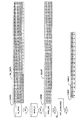
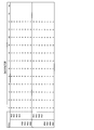
- FIG. 14 is a sequence diagram showing the operation of the product-sum calculator of FIG. 13 in the case of a 3 ⁇ 3 filter.
- FIG. 15 is a sequence diagram showing the selection and non-selection states of the masks Mb0-7 and Mc0-7. With reference to FIGS. 14 and 15, the operation of the product-sum calculator of FIG. 13 will be described.
- the number of pixels in the neighborhood matrix is nine.
- the number of inputs of the product-sum operation unit in FIG. Therefore, nine pixel data and coefficient data cannot be input in one cycle, but are input in two cycles.
- one piece of pixel data and coefficient data are input with a delay of one cycle.
- the sum-of-products calculator has an addition circuit for an overtaking route, and a multiplication value of one pixel data and coefficient data input with a delay of one cycle is a multiplication value of eight pixel data and coefficient data. Can be added at the same stage. Further, the multiplication value of the remaining number of image data and coefficient data input in the next cycle can be added to the multiplication value of any number of pixel data and coefficient data input in the previous cycle.
- the register RG10-17 of the stage ST1 latches the multiplication values of the eight multipliers MP0-7 (multiplication values of a0-a7).
- a0 * w0-a7 * w7 is simply indicated as a0-a7 from the relationship of space.
- the register RG00-07 of the stage ST0 latches the ninth pixel data a8 and the coefficient w8, the second set of seven pixel data b0-b6 and the seven coefficients w0-w6.
- the multiplication value of the ninth pixel data a8 and the coefficient w8 catches up with the multiplication value of the first eight pixel data a0-a7 and the coefficient w0-w7 through the overtaking route.
- the underline, a8 is attached to the pixel data to be caught up with the catch up route.
- Each of the normal root registers RG20-23 of stage ST2 has four sets of addition values a0,1, a2,3, a4,5, a6,7 of the multiplication value of the first set of eight pixel data a0-a7, respectively. Latch. Further, each of the registers RG10-17 of the stage ST1 latches the multiplication value of the first set of 1-pixel data a8 and the second set of 7-pixel data b0-b6. At the same time, the register RG00-07 of the stage ST0 includes the second set of eighth and ninth pixel data b7,8 and coefficients w7,8, and the third set of six pixel data c0-b5 and Latch the coefficients w0-w5.
- Each of the normal root registers RG20-23 of stage ST2 latches four sets of addition values b0, b1, 2, b3,4, b5, 6 of the multiplication value of the second set of 7-pixel data b0-b6, respectively. . Further, each of the registers RG10-17 of the stage ST1 latches the multiplication value of the second set of two-pixel data b7, 8 and the third set of six-pixel data c0-c5. At the same time, the register RG00-07 of the stage ST0 includes the third set of 7-9th pixel data c6-8 and the coefficient w6-8, the fourth set of five pixel data d0-d4 and the five coefficients. Latch w0-w4.
- the register RG40 of the stage ST4 is an addition value a0-8 of the multiplication value of the first set of 9-pixel data a0-a8. Latch.
- the arithmetic unit outputs the added value of the nine pixel data a0 to a8 divided and inputted in cycles 1 and 2 to the added value of the eight pixel data inputted in one cycle.
- An added value of nine pieces of pixel data can be output in the necessary five cycles.
- the added value obtained by adding the pixel data a8 input in cycle 2 can be generated in cycle 5 without being delayed until cycle 6. That is, in cycle 6, it is not necessary to accumulatively add the added value of the 8 pixel data a0-7 and the value of the 1 pixel data a8 by the accumulator ACML.
- the register RG30 of stage ST3 latches the addition value of the addition value b0-2 of the normal route and the values b7 and 8 of the overtaking route, and the register RG31 latches the addition value of the addition value b3-6 of the normal route.
- the added values b7 and 8 delayed by one cycle catch up with the added value of the normal route and are added.
- Each of the normal root registers RG20-23 of stage ST2 latches three sets of addition values c0,1, c2,3, c4,5 of the multiplication value of the third set of 6-pixel data c0-5.
- the adder O_AD20 of the overtaking route adds the multiplication values of the pixel data b7,8.
- each of the registers RG10-17 in the stage ST1 latches the multiplication value of the third set of three-pixel data c6-8 and the fourth set of five-pixel data d0-d4.
- the register RG00-07 of the stage ST0 stores the fourth set of 6-9th pixel data d5-8 and the coefficient w5-8, the fifth set of four pixel data e0-e3 and the four coefficients. Latch w0-w3.
- the register RG50 of the stage ST5 latches the addition value a0-8 of the multiplication value of the first set of 9-pixel data a0-a8. This added value a0-8 becomes the result RESULT of the product-sum calculator.
- the register RG50 latches the added value b0-8 of the multiplication value of the second set of 9-pixel data b0-b8. This added value b0-8 becomes the result RESULT of the product-sum calculator. The same applies hereinafter.
- the normal route mask Mb0-7 and the overtaking route mask Mc0-7 are controlled as follows.
- the masks Mb0-7 for all normal routes are controlled to be “1” selected, and the masks Mc0-7 for all overtaking routes are controlled to be “0” unselected.
- the adder of the overtaking route in stage ST2 does not output a substantial addition value, and the addition value becomes “0”.
- cycle 4 the normal route mask Mb0 is deselected, and the overtaking route mask Mc0 is deselected.
- cycles 5 to 11 after cycle 4 “0” of the normal route mask Mb is incremented by one, and “1” of the overtaking route mask Mc is incremented by one accordingly.
- all are reset in cycle 12, and the same set value as cycle 1 is restored. That is, each of the normal route mask Mb0-7 and the overtaking route mask Mc0-7 selects / deselects the outputs of the registers RG10-17 exclusively based on the control signal CNT.
- the accumulator ACML does not cumulatively calculate the product-sum value of the register RG40.
- FIG. 16 is a sequence diagram showing the operation of the product-sum calculator of FIG. 13 in the case of a 5 ⁇ 5 filter.
- the number of pixels in the neighborhood matrix is 25. Therefore, 25 pixel data and coefficient data cannot be input in one cycle, 24 pixels are input in 8 cycles in 3 cycles, and 1 pixel is input in 1 cycle. Therefore, as described below, the product-sum value of 8 inputs input in 3 cycles is accumulated by the accumulator, and the 1-input multiplication value input in the last 1 cycle is added to the multiplication value of the 3rd cycle in the overtaking route. .
- a product-sum operation of the first set of 25 pixel data a0 to a24 and coefficient data will be described.
- the two sets of 8-input pixel data a0-a7, a8-a15 input in cycles 1 and 2 are summed in a normal route, and accumulated in cycle 7 in the adder AD50 in stage ST5.
- Register RG50 latches. Then, the multiplication value of the set of 8-input pixel data a16-a23 input in cycle 3 and the 1-input pixel data a24 input in cycle 4 is added by the adder AD31 in stage ST3 in cycle 6 by the overtaking route. It is added and latched in the register RG30.
- the register RG40 in stage ST4 latches the product-sum value of the 9-input pixel data a16-a24 in cycle 7
- the adder AD50 in stage ST5 accumulates in cycle 8
- the register RG50 stores 25 pixel data a0- Latch the sum of products of a24.
- the register RG40 in the stage ST4 latches the product-sum value of the 10-input pixel data b15-b24 in the cycle 10
- the adder AD50 in the stage ST5 accumulates the product-sum value in the cycle 11
- the register RG50 latches the product sum value of the 25 pixel data b0 to b24.
- FIG. 17 is a sequence diagram showing the operation of the product-sum calculator when one set of input pixel data is 11 pixels.
- the first set of eleven pixels a0-a10 are input in cycles 1 and 2, and in cycle 5, the register RG40 in stage ST4 latches the product-sum value of the pixel data a0-a10.
- the second set of 11 pixels b0-b10 are input in cycles 2 and 3, and in cycle 6 stage ST4.
- Register RG40 latches the product-sum value of the pixel data b0 to b10.
- the first and second 11 pixel data a0-a10 and b0-b10 are not cumulatively added by the accumulator.
- the third set of 11 pixels c0-c10 is input in cycles 3, 4, and 5. Accordingly, the sum of products of the two pixel data c0,1 input in cycle 3 and the pixel data c2-c9 and c10 input in cycles 4 and 5 is accumulated in cycle 9, and register RG50 in stage ST5 1 The product sum value of the one-pixel data c0 to c10 is latched.
- FIG. 18 is a diagram illustrating a configuration of a product-sum calculator capable of inputting up to 32 pixel data.
- the 32-pixel product-sum operation unit includes four 8-sum product-sum operation units SoP in FIG. 13 arranged in parallel, and further adds an adder ADDER that adds the product-sum values output by the four product-sum operation units SoP.
- An adder ADDER that adds the product-sum values output by the four product-sum operation units SoP.
- Have Four product-sum calculators SoP arranged in parallel each have an overtaking route as described with reference to FIG.
- FIG. 19 is a diagram illustrating a configuration example of the adder ADDER in FIG.
- the adder ADDER includes four input registers RG60-63 that respectively latch the product-sum values of the four product-sum arithmetic units SoP_0-3, and two adders AD70 and AD71 that add the four product-sum values two by two. , Two registers RG70-71 for latching the outputs, an adder AD80 for adding the outputs, and an output register RG80 for latching the outputs.
- the input pixel data shown in FIG. 18 corresponds to a 7 ⁇ 7 filter, and one set is 49 pixel data a0-a48 and b0-b48. Accordingly, one set of 49 pixel data and 49 coefficients w0 to w48 (not shown) are input to the product-sum calculator of FIG. 18 in two cycles.
- the pixel data a32-a48 input in cycle 2 are the pixels input in cycle 1 by the overtaking route of product-sum calculators SoP_0, SoP_1, SoP_2. It is added to the accumulated value of data a0-a31.
- the pixel data b0-b14 input in cycle 2 is accumulated by the accumulator into the pixel data b15-b48 input in cycles 3 and 4 and added in the overtaking route. Is added.
- FIG. 20 is a diagram illustrating a configuration of a product-sum arithmetic unit with an overtaking route in the second embodiment.
- the product-sum operation unit shown in FIG. 20 changes one of the first calculation for calculating the SOA-type image data and the second calculation for calculating the AOS-type image data, as in FIG. can do.
- the second calculation is the calculation shown in FIG.
- the product-sum operation unit in FIG. 20 has a pair of input terminals provided between each of the multipliers MP0-3 in the stage ST1 and each of the registers RG10-17 in addition to the configuration of the product-sum operation unit in FIG. And adders AD10-13, AD14-17 having masks Ma0, 1, Ma2, 3, Ma4, 5, Ma6, 7 and Ma8, 9, Ma10, 11, Ma12, 13, Ma14, 15 and registers RG10-
- a feedback wiring FB is provided between the 17 outputs and the inputs of the selectors SL10-13 and SL14-17.
- the masks Ma0-7 and -7Ma8-15 are the same as the masks Mb0-7 and Mc0-7 in FIG.
- the control signal “1” is input to the odd-numbered masks of the masks Ma0-7 and Ma8-15, and the control signal “0” is input to the even-numbered masks. Is input, and the input of the feedback wiring FB is not selected (input value “0”).
- the product-sum calculator of FIG. 20 is the same as that of FIG.
- the control signals “1” are all input to the masks Ma0-7 and Ma8-15, and the output data of the register RG10-13 of the feedback wiring FB is selected To do.
- the adders AD10-13 and AD14-17 and the registers RG10-13 and RG14-17 form an accumulator.
- FIG. 21 is a diagram illustrating the product-sum calculator of FIG. 20 in the case of the second calculation.
- the product-sum operation unit has eight sets of registers RG00-07 of the input stage ST0, a multiplier MP0-7, an adder AD10-17, and a register RG10-17 of the stage ST1. .
- the multiplication values of the multiplier MP are cumulatively added eight times, and a product-sum operation is performed on each of the 8 sets of 9 pixel data a0-8 to h0-8 and 9 coefficient data w0-8.
- FIG. 22 is a diagram illustrating format conversion for generating AOS pixel data.
- the combiner 44 accumulates eight sets of data data1 generated by the format conversion circuit 40 in the second DMA memory DMA_M1 to generate data data4.
- the transposition circuit TRSP reverses the vertical and horizontal directions of the data data4, and the AOS image data data5 is input to the second high-speed memory SRAM_1.
- 8 sets of 9 pixel data data5 and 9 coefficient data W0-W7 are converted into 8 product-sum calculators SoP shown in FIG. Are input serially in parallel and in synchronization with the clock.
- eight sets of product-sum values features of the pixel of interest in the neighborhood matrix
- a product-sum value is generated in the same clock cycle for a set of data exceeding eight data input in two cycles. be able to. Furthermore, by providing an accumulator at the output of the product-sum operation unit, the product-sum values of the data input in a plurality of cycles can be cumulatively added.
- a processor having an adder circuit that latches an input in synchronization with the input signal
- the computing unit is A plurality of pairs of input registers provided in the input stage and respectively latching a plurality of first input data and a plurality of second input data; A plurality of multipliers each multiplying the first input data and the second input data of each of the plurality of pairs of input registers and latching a multiplication value in each of the plurality of first registers; And The processor according to appendix 1, wherein the multiplier and the adder circuit constitute a product-sum circuit that adds the multiplication values of the plurality of first input data and the plurality of second input data.
- the computing unit is The processor according to appendix 1 or 2, further comprising an accumulator circuit that accumulates the output of the adder circuit in synchronization with the clock.
- the computing unit is A control circuit for setting a first control value for the selection in a mask circuit provided at an input of the first adder and the second adder; When the number of sets of operation target data is larger than the number of the plurality of pairs of input registers, the set of operation target data is divided and input to the plurality of pairs of input registers in a plurality of cycles,
- the control circuit inputs, to the first adder, a first multiplication value of the first input data and the second input data included in the operation target data and input in a first cycle, A second multiplication value of the first input data and the second input data included in the operation target data and input in the second cycle subsequent to the first cycle is input to the second adder.
- the processor according to appendix 2, wherein the first control value is set in the mask circuit.
- the computing unit is A plurality of fourth adders for respectively adding outputs of the plurality of multipliers and outputs of the plurality of first registers between the plurality of multipliers and the plurality of first registers.
- the processor according to claim 2 further comprising: a mask circuit capable of setting a plurality of outputs of the plurality of first registers as one of an input and a non-input at an input of the fourth adder.
- the computing unit is A control circuit for setting the input or non-input second control value in the mask circuit of the plurality of fourth adders;
- the control circuit sets the non-input second control value when the operation target data is in the structure of array format, and sets the input second control value when the operation target data is in the array of structure format.
- the processor according to appendix 5, which is set.
- the plurality of first input data is a plurality of pixel data of a neighborhood matrix of image data
- the plurality of second input data is a plurality of coefficient data of a coefficient matrix corresponding to the neighborhood matrix
- the processor according to claim 2 wherein the product-sum circuit calculates a product-sum value of the plurality of pixel data of the neighborhood matrix and the plurality of coefficient data of the coefficient matrix.
- a processor A main memory accessed by the processor;
- the processor is Multiple processor cores, An internal memory accessed from the plurality of processor cores,
- the arithmetic unit included in any of the plurality of processor cores is A plurality of first registers provided in the first stage;
- a normal adder circuit comprising: a first adder for adding a plurality of outputs of the plurality of first registers; and a second register provided in a second stage for latching the output of the first adder;
- An overtaking circuit having a second adder for adding a plurality of outputs of the plurality of first registers;
- a synthesis circuit having a third adder for adding the output of the normal adder circuit and the output of the overtaking adder circuit, and a third register provided in a third stage for latching the output of the second adder
- the first adder and the second adder select and input a plurality of outputs of the plurality of first registers mutually exclusive, and the first, second, and third registers are clocks
- Arithmetic unit included in any of the plurality of processor cores is A plurality of first registers provided in the first stage;
- a normal adder circuit comprising: a first adder for adding a plurality of outputs of the plurality of first registers; and a second register provided in a second stage for latching the output of the first adder;
- An overtaking circuit having a second adder for adding a plurality of outputs of the plurality of first registers;
- a synthesis circuit having a third adder for adding the output of the normal adder circuit and the output of the overtaking adder circuit, and a third register provided in a third stage for latching the output of the second adder
- a method of operating a processor having an adder circuit comprising: The first adder and the second adder select and input a plurality of outputs of the plurality of first registers mutually exclusive, The first, second, and third registers latch inputs in synchronization with a
- RG Register MK: Mask, mask circuit MP: Multiplier AD: Adder SL: Selector 52: Control state machine, control circuit RG00-03, RG04-07: Input registers RG10-13, RG14-17: First register RG20,21, RG22,23: Second register RG30,31: Third register OCTK_0,1: Overtake adder circuit RGL_0,1: Normal adder circuit ACML: Accumulator, cumulative adder
Landscapes
- Engineering & Computer Science (AREA)
- Physics & Mathematics (AREA)
- Theoretical Computer Science (AREA)
- General Physics & Mathematics (AREA)
- Computing Systems (AREA)
- General Engineering & Computer Science (AREA)
- Mathematical Optimization (AREA)
- Pure & Applied Mathematics (AREA)
- Mathematical Analysis (AREA)
- Computational Mathematics (AREA)
- Mathematical Physics (AREA)
- Software Systems (AREA)
- Data Mining & Analysis (AREA)
- Biophysics (AREA)
- Biomedical Technology (AREA)
- Life Sciences & Earth Sciences (AREA)
- Health & Medical Sciences (AREA)
- Computational Linguistics (AREA)
- Artificial Intelligence (AREA)
- Molecular Biology (AREA)
- General Health & Medical Sciences (AREA)
- Evolutionary Computation (AREA)
- Databases & Information Systems (AREA)
- Algebra (AREA)
- Nonlinear Science (AREA)
- Computer Hardware Design (AREA)
- Neurology (AREA)
- Image Processing (AREA)
- Advance Control (AREA)
- Complex Calculations (AREA)
Abstract
複数のプロセッサコアと、複数のプロセッサコアからアクセスされる内部メモリとを有し、複数のプロセッサコアのいずれかが有する演算器は、第1ステージに設けられた複数の第1のレジスタと、複数の第1のレジスタの複数の出力を加算する第1の加算器と、第2ステージに設けられ前記第1の加算器の出力をラッチする第2のレジスタとを有する通常加算回路と、複数の第1のレジスタの複数の出力を加算する第2の加算器を有する追越し加算回路と、前記通常加算回路の出力と前記追越し加算回路の出力とを加算する第3の加算器と、第3ステージに設けられ前記第3の加算器の出力をラッチする第3のレジスタとを有する合成回路とを有し、第1の加算器と第2の加算器は、複数の第1のレジスタの複数の出力を互いに排他的に選択して入力する、加算回路を有する、プロセッサ。
Description
本発明は,プロセッサ、情報処理装置及びプロセッサの動作方法に関する。
ディープラーニング(以下DL1:Deep Learning)は、情報処理装置内のプロセッサの演
算処理により実行される。DLは、階層の深いニューラルネットワーク(以下DNN:Deep Neural Network)を利用したアルゴリズムの総称である。そして、DNNの中でも良く利用さ
れるのが、コンボリュージョン・ニューラルネットワーク(CNN:ConvolutionNeural Network)である。CNNは、例えば画像データの特徴を判定するDNNとして広く利用される。
算処理により実行される。DLは、階層の深いニューラルネットワーク(以下DNN:Deep Neural Network)を利用したアルゴリズムの総称である。そして、DNNの中でも良く利用さ
れるのが、コンボリュージョン・ニューラルネットワーク(CNN:ConvolutionNeural Network)である。CNNは、例えば画像データの特徴を判定するDNNとして広く利用される。
画像データの特徴を判定するCNNは、画像データを入力しフィルタを利用した畳込み演
算を行い画像データの特徴(例えばエッジの特徴など)を検出する。そして、CNNの畳込
み演算は、例えばプロセッサにより演算される。以下の特許文献1にはメモリのデータフォーマットと演算器の実行性能について開示がある。
算を行い画像データの特徴(例えばエッジの特徴など)を検出する。そして、CNNの畳込
み演算は、例えばプロセッサにより演算される。以下の特許文献1にはメモリのデータフォーマットと演算器の実行性能について開示がある。
上記の畳込み演算は、係数フィルタの画像データでの位置を画像データのラスタスキャン方向に移動しながら、画像データの注目画素を中心とする近傍マトリクスの画素データと係数フィルタの係数(重み)との積和演算を繰り返す。係数フィルタのサイズは、一般に、奇数の二乗(8の倍数に1加算した値)である。例えば、3×3、5×5、7×7、9×9、11×11などである。
一方、畳込み演算は、積和演算の繰り返しであり、複数の積和演算器で並列処理することが望ましい。また、DNNでは複数チャネルの画像データ(複数プレーンの画素データ)
に対して畳込み演算を行う場合があり、その場合も複数の積和演算器で並列処理することが望ましい。
に対して畳込み演算を行う場合があり、その場合も複数の積和演算器で並列処理することが望ましい。
ところが、プロセッサは一般に2のべき乗個の演算器を有する。そのため、例えば16個の演算器に、3×3の係数フィルタの場合の9個の係数や画素データを入力すると、一部の演算器が積和演算を処理できない場合があり、その結果、16個の演算器を効率的に動作させることができない。
そのため、画像データを転置して、複数組の画素データとその係数を並列に16個の演算器に入力することが行われる。しかし、その場合は、画像データを転置する処理が必要になり、転置処理の間演算器が動作を停止する必要があるので、やはり16個の演算器を効率的に動作させることができない。
そこで、一つの実施の形態の目的は,効率的に演算を行うプロセッサ、情報処理装置及びプロセッサの動作方法を提供することにある。
一つの実施の形態は,
複数のプロセッサコアと、
前記複数のプロセッサコアからアクセスされる内部メモリとを有し、
前記複数のプロセッサコアのいずれかが有する演算器は、
第1ステージに設けられた複数の第1のレジスタと、
前記複数の第1のレジスタの複数の出力を加算する第1の加算器と、第2ステージに設けられ前記第1の加算器の出力をラッチする第2のレジスタとを有する通常加算回路と、
前記複数の第1のレジスタの複数の出力を加算する第2の加算器を有する追越し加算回路と、
前記通常加算回路の出力と前記追越し加算回路の出力とを加算する第3の加算器と、第3ステージに設けられ前記第2の加算器の出力をラッチする第3のレジスタとを有する合成回路とを有し、
前記第1の加算器と前記第2の加算器は、前記複数の第1のレジスタの複数の出力を互いに排他的に選択して入力し、前記第1、第2、第3のレジスタはクロックに同期して入力をラッチする、加算回路を有する、プロセッサである。
複数のプロセッサコアと、
前記複数のプロセッサコアからアクセスされる内部メモリとを有し、
前記複数のプロセッサコアのいずれかが有する演算器は、
第1ステージに設けられた複数の第1のレジスタと、
前記複数の第1のレジスタの複数の出力を加算する第1の加算器と、第2ステージに設けられ前記第1の加算器の出力をラッチする第2のレジスタとを有する通常加算回路と、
前記複数の第1のレジスタの複数の出力を加算する第2の加算器を有する追越し加算回路と、
前記通常加算回路の出力と前記追越し加算回路の出力とを加算する第3の加算器と、第3ステージに設けられ前記第2の加算器の出力をラッチする第3のレジスタとを有する合成回路とを有し、
前記第1の加算器と前記第2の加算器は、前記複数の第1のレジスタの複数の出力を互いに排他的に選択して入力し、前記第1、第2、第3のレジスタはクロックに同期して入力をラッチする、加算回路を有する、プロセッサである。
第1の側面によれば,効率的に演算を行うことができる。
図1は、本実施の形態におけるディープラーニングを実行する情報処理装置(ディープラーニングサーバ)の構成を示す図である。サーバ1は、ネットワークを介してセンシング装置群30及び端末装置32と通信可能である。センシング装置群30は、例えば撮像素子により画像を撮像して画像データを生成し、画像データをサーバ1に送信する。端末装置32は、画像データの特徴の判定結果をサーバ1から受信して出力する。
サーバ1は、汎用プロセッサであるCPU(Centralprocessing Unit)10と、グラフィックプロセッサであるGPU(Graphic Processing Unit)11とを有する。サーバ1は、さらに、DRAMなどのメインメモリ12と、NIC(Network Interface Card)などのネットワ
ークインターフェース14と、ハードディスクやSSD(SolidStorage Device)などの大
容量の補助メモリ20と、それらを接続するバスBUSとを有する。
ークインターフェース14と、ハードディスクやSSD(SolidStorage Device)などの大
容量の補助メモリ20と、それらを接続するバスBUSとを有する。
補助メモリ20は、ディープラーニング演算プログラム22と、ディープラーニングパラメータ24などを記憶する。補助メモリ20は、上記プログラムやパラメータに加えて、図示しないオペレーティングシステム(OS)や、各種ミドルウエアプログラムなども記憶する。プロセッサ10及びグラフィックプロセッサ11は、上記のプログラムやパラメータをメインメモリ12に展開し、パラメータに基づいてプログラムを実行する。
図2は、ディープラーニング演算プログラムの概略的な処理を示すフローチャート図である。DL演算プログラムは、例えばDNNの演算を実行するプログラムである。プロセッサ
10,11は、DL演算プログラムを実行して、学習モードと判定モードの処理を実行する。DLとして、画像データの特徴を判定するDNNを例にして説明する。
10,11は、DL演算プログラムを実行して、学習モードと判定モードの処理を実行する。DLとして、画像データの特徴を判定するDNNを例にして説明する。
学習モードでは、プロセッサ10、11は、演算パラメータ(フィルタの係数(重み)等)の初期値をメインメモリ12から読み出し、プロセッサ11内の高速メモリSRAMに書込む(S10)。さらに、プロセッサは、センシング装置群30から送信された画像データ
をメインメモリ12から読み出し高速メモリSRAMに書込む(S11)。そして、プロセッサ
は、画像データをフォーマット変換して演算器入力用の近傍マトリクス画像データ(演算処理データ)を生成し(S12)、DNNの畳込み層、プーリング層、全結合層、ソフトマックス層(出力層)の演算処理を行う(S13)。この演算は、所定数の画像データについてそ
れぞれ行われる。演算結果は例えば画像データが数字0~1のうちいずれかなどである。
をメインメモリ12から読み出し高速メモリSRAMに書込む(S11)。そして、プロセッサ
は、画像データをフォーマット変換して演算器入力用の近傍マトリクス画像データ(演算処理データ)を生成し(S12)、DNNの畳込み層、プーリング層、全結合層、ソフトマックス層(出力層)の演算処理を行う(S13)。この演算は、所定数の画像データについてそ
れぞれ行われる。演算結果は例えば画像データが数字0~1のうちいずれかなどである。
更に、プロセッサ10、11は、演算結果と画像データの正解データである教師データとの差分が閾値以下か否か判定し(S14)、差分が閾値以下でない場合(S14のNO)、演算パラメータを差分に基づいてDNNのバックワード演算を実行し演算パラメータを更新する
(S15)。そして、更新された演算パラメータで、上記の工程S11-S13を繰り返す。ここで演算結果と教師データとの差分は、例えば1000枚の画像データについて演算した1000個の演算結果と、1000個の教師データそれぞれの差分の合計値などである。
(S15)。そして、更新された演算パラメータで、上記の工程S11-S13を繰り返す。ここで演算結果と教師データとの差分は、例えば1000枚の画像データについて演算した1000個の演算結果と、1000個の教師データそれぞれの差分の合計値などである。
上記の差分が閾値以下になったとき(S14のYES)、演算パラメータが最適値に設定されたと判断して、学習モードを終了する。そして、演算パラメータの最適値によって、その後の判定モードでの演算処理が行われる。
判定モードでは、プロセッサ10、11は、判定対象の画像データをメインメモリから読み出し(S16)、画像データをフォーマット変換して演算器入力用の近傍マトリクス画
像データを生成し(S17)、DNNの畳込み層、プーリング層、全結合層、ソフトマックス層の演算処理を行う(S18)。プロセッサ10,11は、上記の判定処理を、判定対象の画
像データが終了するまで繰り返す(S19)。判定結果は、端末装置32に送信され出力さ
れる。
像データを生成し(S17)、DNNの畳込み層、プーリング層、全結合層、ソフトマックス層の演算処理を行う(S18)。プロセッサ10,11は、上記の判定処理を、判定対象の画
像データが終了するまで繰り返す(S19)。判定結果は、端末装置32に送信され出力さ
れる。
図3は、グラフィックプロセッサ(GPU)11の構成とGPU内のコアCOREの構成とを示す図である。GPU11は、メインメモリM_MEMにアクセス可能である。GPUは、例えば8個のプロセッサコアCOREと、それぞれのプロセッサコアCOREに対応して配置された複数の高速メモリSRAMと、内部バスI_BUSと、メインメモリM_MEMとのアクセス制御を行うメモリコントローラMCとを有する。GPUは、図3に示されていない、各コアCORE内のL1キャッシュメモ
リと、8つのコアCOREで共用されるL2キャッシュメモリと、種々の周辺リソース回路を有する。さらに、GPUは、内部の高速メモリSRAM間のデータ転送、メインメモリM_MEMと高速メモリSRAM間のデータ転送などを制御するダイレクトメモリアクセス制御回路DMAを有す
る。
リと、8つのコアCOREで共用されるL2キャッシュメモリと、種々の周辺リソース回路を有する。さらに、GPUは、内部の高速メモリSRAM間のデータ転送、メインメモリM_MEMと高速メモリSRAM間のデータ転送などを制御するダイレクトメモリアクセス制御回路DMAを有す
る。
一方、各プロセッサコアCOREは、通常のプロセッサコアと同様に、命令をメモリから取得する命令フェッチ回路FETCHと、取得した命令をデコードするデコーダDECと、デコード結果に基づいて命令を演算する複数の演算器ALU及びそのレジスタ群REGと、高速メモリSRAMにアクセスするメモリアクセス制御回路MACとを有する。
GPUは、例えば半導体チップで実現され、本実施の形態のDL装置である。GPUは、前述のセンシング装置群から送信された画像データを記憶するメインメモリM_MEMから画像デー
タを読み出して、内部の高速メモリSRAMに書込む。そして、各コアCORE内の演算器ALUは
、SRAMに書き込まれた画像データを入力し、DNNの各層の演算処理を実行し、DNNの出力を生成する。
タを読み出して、内部の高速メモリSRAMに書込む。そして、各コアCORE内の演算器ALUは
、SRAMに書き込まれた画像データを入力し、DNNの各層の演算処理を実行し、DNNの出力を生成する。
図4は、CNNの一例を示す図である。画像データの判定処理を行うCNNは、入力データである画像データIM_Dが入力される入力層INPUT_Lと、複数組のコンボリュージョン層CNV_L及びプーリング層PL_Lと、全結合層C_Lと、ソフトマックス層(出力層)OUT_Lとを有する。
コンボリュージョン層CNV_Lは、画像データIM_Dを係数フィルタFLTでフィルタリングしてある特徴量を有する画像データF_IM_Dを生成する。複数の係数フィルタFLT_0-3でフィ
ルタリングすると、それぞれの特徴量の画像データF_IM_Dが生成される。プーリング層PL_Lは、例えばコンボリュージョン層のノードの値の代表値(例えば最大値)を選択する。そして、出力層OUT_Lには、前述したように、例えば画像データ内の数字の判定結果(0
~9のいずれか)が出力される。
ルタリングすると、それぞれの特徴量の画像データF_IM_Dが生成される。プーリング層PL_Lは、例えばコンボリュージョン層のノードの値の代表値(例えば最大値)を選択する。そして、出力層OUT_Lには、前述したように、例えば画像データ内の数字の判定結果(0
~9のいずれか)が出力される。
コンボリュージョン層CNV_Lは、M×Nの二次元画素マトリクスの画素データを有する画
像データIM_Dの例えば3×3の近傍マトリクスの画素データと、近傍マトリクスと同じ3×3の係数フィルタFLTの係数データとをそれぞれ乗算し乗算結果を加算する積和演算を
行い、近傍マトリクスの中央の注目画素の画素データF_IM_Dを生成する。このフィルタリング処理を、係数フィルタを画像データIM_Dのラスタスキャン方向にずらしながら画像データIM_Dの全ての画素に対して演算を行う。これが畳込み演算である。
像データIM_Dの例えば3×3の近傍マトリクスの画素データと、近傍マトリクスと同じ3×3の係数フィルタFLTの係数データとをそれぞれ乗算し乗算結果を加算する積和演算を
行い、近傍マトリクスの中央の注目画素の画素データF_IM_Dを生成する。このフィルタリング処理を、係数フィルタを画像データIM_Dのラスタスキャン方向にずらしながら画像データIM_Dの全ての画素に対して演算を行う。これが畳込み演算である。
図5は、畳込み演算を説明する図である。図5には、例えば5行5列の画像データの周囲にパディングPを追加した入力画像データIN_DATAと、3行3列の重みW0-W8を有する係
数フィルタFLT0と、畳込み演算された出力画像データOUT_DATAとが示される。畳込み演算は、注目画素を中心とする近傍マトリクスの複数の画素データと係数フィルタFLT0の複数の係数(重み)W0-W8とをそれぞれ乗算し加算する積和演算を、係数フィルタFLT0を画像
データのラスタスキャン方向にずらしながら繰り返す演算である。
数フィルタFLT0と、畳込み演算された出力画像データOUT_DATAとが示される。畳込み演算は、注目画素を中心とする近傍マトリクスの複数の画素データと係数フィルタFLT0の複数の係数(重み)W0-W8とをそれぞれ乗算し加算する積和演算を、係数フィルタFLT0を画像
データのラスタスキャン方向にずらしながら繰り返す演算である。
近傍マトリクスの画素データがXi(但しi=0-8)、係数フィルタの係数データがWi(但
しi=0-8)の場合、積和演算式は次のとおりである。
Xi = Σ(Xi * Wi) (1)
但し、右辺のXiは入力画像IN_DATAの画素データ、Wiは係数であり、Σはi = 0-8 だけ加
算することを示し、左辺のXiは積和演算値であり出力画像OUT_DATAの画素データである。
しi=0-8)の場合、積和演算式は次のとおりである。
Xi = Σ(Xi * Wi) (1)
但し、右辺のXiは入力画像IN_DATAの画素データ、Wiは係数であり、Σはi = 0-8 だけ加
算することを示し、左辺のXiは積和演算値であり出力画像OUT_DATAの画素データである。
即ち、画像データの注目画素がX6の場合は、式(1)により積和演算SoPされた画素デ
ータX6は、次のとおりである。
X6 = X0*W0 + X1*W1 + X2*W2 + X5*W3 + X6*W4 + X7*W5 + X10*W6 + X11*W7 + X12*W8
図6は、メモリに記憶されるデータ構造の配列(AOS:ArrayOf Structure)を16個
の演算器に入力する例を示す図である。図6では、入力データIN_DATAは、アレイオブス
トラクチャ(AOS)形式である各行16ワードの入力画像データIN_DATAと、16ワードの係数FLT(W0-W8)を、行の順に16個の演算器ALUに入力する例である。
ータX6は、次のとおりである。
X6 = X0*W0 + X1*W1 + X2*W2 + X5*W3 + X6*W4 + X7*W5 + X10*W6 + X11*W7 + X12*W8
図6は、メモリに記憶されるデータ構造の配列(AOS:ArrayOf Structure)を16個
の演算器に入力する例を示す図である。図6では、入力データIN_DATAは、アレイオブス
トラクチャ(AOS)形式である各行16ワードの入力画像データIN_DATAと、16ワードの係数FLT(W0-W8)を、行の順に16個の演算器ALUに入力する例である。
入力画像データIN_DATAは、各行、最初の9ワードに画素データa0-a8、b0-b8、c0-c8、d0-d8を、残りの7ワードに値「0」の画素データをパッキングされている。また、係数
フィルタFLTも、1行に、最初の9ワードに係数データW0-W8を、残りの7ワードに値「0
」をパッキングされている。そして、それぞれ対応する列の画素データと係数データの対が、演算器ALUの16個の入力に入力される。
フィルタFLTも、1行に、最初の9ワードに係数データW0-W8を、残りの7ワードに値「0
」をパッキングされている。そして、それぞれ対応する列の画素データと係数データの対が、演算器ALUの16個の入力に入力される。
この場合、演算器のうち9個の入力の演算器は有効な入力データについて演算を行うが、残りの7個の入力の演算器は無効な入力データであるので有効な演算を行っていない。
図7は、メモリに記憶されるデータ構造の配列であるAOSを転置したストラクチャオブ
アレイ(SOA:Structure Of Array)のデータを4個の演算器に入力する例を示す図である。入力データIN_DATAと係数フィルタFLTの係数データW0-W8は、図6と同じである。この
入力データIN_DATAの列方向と行方向を転置処理により逆にした転置後データTRSP_DATAが、係数データと対で、4個の演算器ALUに入力される。
アレイ(SOA:Structure Of Array)のデータを4個の演算器に入力する例を示す図である。入力データIN_DATAと係数フィルタFLTの係数データW0-W8は、図6と同じである。この
入力データIN_DATAの列方向と行方向を転置処理により逆にした転置後データTRSP_DATAが、係数データと対で、4個の演算器ALUに入力される。
この場合、4個の演算器は全て有効な入力データを入力して演算を行う。したがって、無効な演算を行う演算器をなくすことができ、演算効率を高めることができる。しかしながら、4この演算器は、入力データの転置処理が完了するまで、演算処理を開始することができず、演算効率の低下を招く。
[第1の実施の形態]
図8は、本実施の形態における演算器の入力データの構成を図6,図7の例と対比して示す図である。図6、図7に示した入力データの構成AOS, SOAは、図8の(B)(C)に示される。図8には、演算器のへ入力されるデータは、簡単のために入力データIN_DATAだ
けを示し、フィルタの係数は省略している。
図8は、本実施の形態における演算器の入力データの構成を図6,図7の例と対比して示す図である。図6、図7に示した入力データの構成AOS, SOAは、図8の(B)(C)に示される。図8には、演算器のへ入力されるデータは、簡単のために入力データIN_DATAだ
けを示し、フィルタの係数は省略している。
図8(B)は、図6と異なり演算器ALUの16の入力が右側に縦方向に並べて示され、図8(C)は、図7と異なり16個の演算器ALUが右側に縦方向に並べて示される。(B)の
場合、入力データのフォーマットはAOSであるため、16個の入力のうち7つの入力の演
算器ALUが稼働していない。一方、(C)の場合、入力データのフォーマットはSOAである
ため、16個の演算器ALUはフル稼働するが、SOAへのフォーマット化のために転置処理が
必要になり、演算開始まで処理のサイクル演算器の動作が停止する。
場合、入力データのフォーマットはAOSであるため、16個の入力のうち7つの入力の演
算器ALUが稼働していない。一方、(C)の場合、入力データのフォーマットはSOAである
ため、16個の演算器ALUはフル稼働するが、SOAへのフォーマット化のために転置処理が
必要になり、演算開始まで処理のサイクル演算器の動作が停止する。
それに対して、図8(A)は、本実施の形態の入力データの構成と4個の演算器が示さ
れる。この場合、演算器ALUの8個の入力には9個の画素データa0-a8が8ワード幅で入力される。そのため、最初の8ワード入力には8個の画素データa0-a7が含まれ、次の8ワ
ード入力には残りの画素データa8が、次の9個の画素データの一部b0-b6と共に含まれる。
れる。この場合、演算器ALUの8個の入力には9個の画素データa0-a8が8ワード幅で入力される。そのため、最初の8ワード入力には8個の画素データa0-a7が含まれ、次の8ワ
ード入力には残りの画素データa8が、次の9個の画素データの一部b0-b6と共に含まれる。
そこで、本実施の形態における演算器ALUは、入力数を超える個数の入力データを複数
のサイクルで入力し、最初のサイクルで入力したデータの演算サイクル数後に全入力データの演算結果を出力する。例えば、演算器は、複数のステージでパイプライン処理して演算結果を出力する。本実施の形態における演算器は、通常のパイプライン処理ルートに加えて、通常よりもステージ数が少ない追越し処理ルートを有する。そして、最初の8ワード入力に収まらなかった入力データの演算を追越し処理ルートで実行し、最初のサイクルで入力したデータの演算サイクル数後に、全入力データの演算結果を出力する。
のサイクルで入力し、最初のサイクルで入力したデータの演算サイクル数後に全入力データの演算結果を出力する。例えば、演算器は、複数のステージでパイプライン処理して演算結果を出力する。本実施の形態における演算器は、通常のパイプライン処理ルートに加えて、通常よりもステージ数が少ない追越し処理ルートを有する。そして、最初の8ワード入力に収まらなかった入力データの演算を追越し処理ルートで実行し、最初のサイクルで入力したデータの演算サイクル数後に、全入力データの演算結果を出力する。
[GPUの構成]
図9は、本実施の形態におけるグラフィックプロセッサGPU(DL装置)の構成を示す図
である。図9のGPUは、図3の構成を簡略化した構成を示している。GPUはDL演算を行うDLチップ(DL装置)である。
図9は、本実施の形態におけるグラフィックプロセッサGPU(DL装置)の構成を示す図
である。図9のGPUは、図3の構成を簡略化した構成を示している。GPUはDL演算を行うDLチップ(DL装置)である。
GPUは、プロセッサコアCOREと、内部の高速メモリSRAM_0, SRAM_1と、内部バスI_BUSと、メモリコントローラMCと、更に、画像データのフォーマット変換器FMT_Cと、制御バスC_BUSとを有する。フォーマット変換器FMT_Cは、メインメモリM_MEMから入力した画像データを、コアCORE内の演算器に入力するための入力用の近傍マトリクス画像データに、フォーマット変換する。本実施の形態では、フォーマット変換器FMT_Cは、高速メモリSRAM_0,
SRAM_1間のデータ転送を実行するDMAである。つまり、DMAは、本来のデータ転送回路に
加えて、フォーマット変換器を有する。但し、フォーマット変換器は、DMAとは別に単独
で構成してもよい。そして、DMAは、高速メモリSRAM_0の画像データを入力し、フォーマ
ット変換して生成した近傍マトリクス画像データを別の高速メモリSRAM_1に書込む。
SRAM_1間のデータ転送を実行するDMAである。つまり、DMAは、本来のデータ転送回路に
加えて、フォーマット変換器を有する。但し、フォーマット変換器は、DMAとは別に単独
で構成してもよい。そして、DMAは、高速メモリSRAM_0の画像データを入力し、フォーマ
ット変換して生成した近傍マトリクス画像データを別の高速メモリSRAM_1に書込む。
プロセッサコアCOREは、積和演算器を内蔵する。積和演算器は、フォーマット変換器が生成した近傍マトリクス画像データと、係数フィルタの係数データとを乗算しそれぞれ加算する。
[入力データのフォーマット変換例]
図10は、フォーマット変換器FMT_Cの構成を示す図である。フォーマット変換器FMT_Cは、制御バスC_BUSの制御バスインターフェースC_BUS_IFと、制御データを格納する制御
データレジスタCNT_REGと、ステートマシンのような制御回路CNTとを有する。制御バスC_BUSには図示しないコアから制御データが転送され、制御レジスタに制御データが格納さ
れる。
図10は、フォーマット変換器FMT_Cの構成を示す図である。フォーマット変換器FMT_Cは、制御バスC_BUSの制御バスインターフェースC_BUS_IFと、制御データを格納する制御
データレジスタCNT_REGと、ステートマシンのような制御回路CNTとを有する。制御バスC_BUSには図示しないコアから制御データが転送され、制御レジスタに制御データが格納さ
れる。
制御回路CNTは、第1の高速メモリSRAM_0から第2の高速メモリSRAM_1への画像データ
の転送の制御を行う。また、制御回路CNTは、画像データのフォーマット変換の場合、前
記画像データの転送制御に加えて、パラメータレジスタ42へのパラメータ値の設定と、フォーマット変換の開始と終了の制御を行う。つまり、制御回路CNTは、第1の高速メモ
リSRAM_0から画像データを読み出し、フォーマット変換し、第2の高速メモリSRAM_1へ書き込む。このように、制御回路CNTは、画像データのデータ転送中にフォーマット変換を
行う。制御回路は、データ転送を行うとき、画像データのアドレスを指定して高速メモリSRAMへのアクセスを行う。そして、制御回路は、画像データのアドレスに対応して、フォーマット変換に必要なレジスタのパラメータ値を設定する。
の転送の制御を行う。また、制御回路CNTは、画像データのフォーマット変換の場合、前
記画像データの転送制御に加えて、パラメータレジスタ42へのパラメータ値の設定と、フォーマット変換の開始と終了の制御を行う。つまり、制御回路CNTは、第1の高速メモ
リSRAM_0から画像データを読み出し、フォーマット変換し、第2の高速メモリSRAM_1へ書き込む。このように、制御回路CNTは、画像データのデータ転送中にフォーマット変換を
行う。制御回路は、データ転送を行うとき、画像データのアドレスを指定して高速メモリSRAMへのアクセスを行う。そして、制御回路は、画像データのアドレスに対応して、フォーマット変換に必要なレジスタのパラメータ値を設定する。
フォーマット変換器FMT_Cは、更に、第1のDMAメモリDMA_M0と、第2のDMAメモリDMA_M1と、それらメモリの間にフォーマット変換回路40と、コンカテネーション(結合回路
)44を有する。これらのフォーマット変換回路40及び結合回路44は、複数組設けられ、複数組の近傍マトリクス画像データのフォーマット変換を並列に行う。また、結合回路のパラメータを設定する結合回路パラメータレジスタ42を有する。そして、画像データの転置を行う転置回路TRSPと、内部バスI_BUSのデータバスD_BUSと接続されるデータバスインターフェースD_BUS_IFとを有する。
)44を有する。これらのフォーマット変換回路40及び結合回路44は、複数組設けられ、複数組の近傍マトリクス画像データのフォーマット変換を並列に行う。また、結合回路のパラメータを設定する結合回路パラメータレジスタ42を有する。そして、画像データの転置を行う転置回路TRSPと、内部バスI_BUSのデータバスD_BUSと接続されるデータバスインターフェースD_BUS_IFとを有する。
そして、演算器ALUを内蔵するコアCOREは、第2の高速メモリSRAM_1に保存されているフォーマット変換後の近傍マトリクス画像データを読み出し、内蔵する積和演算器が畳込み演算を実行し、演算後の特徴量データを、再び高速メモリに書込む。
図11、図12は、積和演算器に入力する入力用の近傍マトリクスの画像データの生成手順の第1例を示す図である。メインメモリM_MEMは1行32ワード幅で13行13列の画像データIM_DATAを記憶する。画像データIM_DATAには32列のコラムアドレスCADD(=0-31)が示される。一方、13行13列の画像データIM_DATAは、169ワードの画素データX0-X168を有する。
まず、GPU内のメモリコントローラMCが、メインメモリM_MEM内の画像データIM_DATAを
32ワード幅の外部バスを介して読み出し、32ワード幅を16ワード幅に変換し、16ワード幅の内部バスI_BUSを介して第1の高速メモリSRAM_0に書き込む。このデータ転送
は、例えばDMAの標準のデータ転送機能により行われる。
32ワード幅の外部バスを介して読み出し、32ワード幅を16ワード幅に変換し、16ワード幅の内部バスI_BUSを介して第1の高速メモリSRAM_0に書き込む。このデータ転送
は、例えばDMAの標準のデータ転送機能により行われる。
次に、フォーマット変換器であるDMAが、第1の高速メモリSRAM_0内の画像データを内
部バスI_BUSを介して読み出し、第1のDMAメモリDMA_M0に書き込む。そして、データフォーマット変換回路40が、第1のDMAメモリ内の画像データdata0から近傍マトリクスの9画素データを抽出し、16ワードのデータdata1を生成する。
部バスI_BUSを介して読み出し、第1のDMAメモリDMA_M0に書き込む。そして、データフォーマット変換回路40が、第1のDMAメモリ内の画像データdata0から近傍マトリクスの9画素データを抽出し、16ワードのデータdata1を生成する。
次に、図12に示すとおり、結合回路CONCが、8組の近傍マトリクス画像データdata2
それぞれの1組9ワードの画素データを、1行16ワードの第2のDMAメモリDMA_M1にラ
スタスキャン方向に詰めてパッキングする。その結果、1組目の近傍マトリクス画像データa0-a8は、第2のDMAメモリの1行目と2行目にまたがって格納され、2組目の近傍マトリクス画像データb0-b8は2行目と3行目にまたがって格納され、3組目以降のそれぞれ
9ワードの近傍マトリクス画像データが2行にまたがって格納される。
それぞれの1組9ワードの画素データを、1行16ワードの第2のDMAメモリDMA_M1にラ
スタスキャン方向に詰めてパッキングする。その結果、1組目の近傍マトリクス画像データa0-a8は、第2のDMAメモリの1行目と2行目にまたがって格納され、2組目の近傍マトリクス画像データb0-b8は2行目と3行目にまたがって格納され、3組目以降のそれぞれ
9ワードの近傍マトリクス画像データが2行にまたがって格納される。
そして、制御回路CNTは、第2のDMAメモリDMA_M1内の近傍マトリクス画像データをパッキングした画像データdata2を、転置処理せずに、内部バスを介して第2の高速メモリSRAM_1に転送する。
次に、GPU内のコアCOREが、第2の高速メモリSRAM_1内の近傍マトリクス画像データdata3を16ワードずつ読み出し、16ワードを8ワードずつに変換し、データdata3を生成
する。そして、コアCORE内に設けられた単一の積和演算器SoPの第1ステージの8個の乗
算器MLTPに、近傍マトリクス画像データを8ワードずつ、係数(W0-W8)と共に入力する
。その結果、積和演算器SoPは、9ワードの近傍マトリクスの画素データのうち8ワード
ずつ係数と乗算し、乗算結果を加算して積和演算結果を出力する。なお、積和演算器SoP
は、2行目の残りの画素データ(図中例えばa8)については、係数との乗算値を図示しない追い越し回路により1行目の8ワードの積和値に加算する。
する。そして、コアCORE内に設けられた単一の積和演算器SoPの第1ステージの8個の乗
算器MLTPに、近傍マトリクス画像データを8ワードずつ、係数(W0-W8)と共に入力する
。その結果、積和演算器SoPは、9ワードの近傍マトリクスの画素データのうち8ワード
ずつ係数と乗算し、乗算結果を加算して積和演算結果を出力する。なお、積和演算器SoP
は、2行目の残りの画素データ(図中例えばa8)については、係数との乗算値を図示しない追い越し回路により1行目の8ワードの積和値に加算する。
コアCORE内の積和演算器SoPは、フォーマット変換された第2のDMAメモリDMA_M1内の近
傍マトリクス画像データを、転置処理せずに、そのまま入力するので、演算開始までに待機するサイクルがなく、演算器の稼働率を高くすることができる。
傍マトリクス画像データを、転置処理せずに、そのまま入力するので、演算開始までに待機するサイクルがなく、演算器の稼働率を高くすることができる。
[追越しルート付積和演算器]
図13は、本実施の形態の追越しルート付積和演算器の構成を示す図である。図13の積和演算器は、パイプラインステージST0-ST5を有し、各パイプラインステージに複数ま
たは単数のレジスタRGを有し、各ステージのレジスタRGには図示しないクロックが供給され、クロック入力に応答して入力データをラッチする。
図13は、本実施の形態の追越しルート付積和演算器の構成を示す図である。図13の積和演算器は、パイプラインステージST0-ST5を有し、各パイプラインステージに複数ま
たは単数のレジスタRGを有し、各ステージのレジスタRGには図示しないクロックが供給され、クロック入力に応答して入力データをラッチする。
まず、正規ルートによる積和演算器の構成を説明し、その後、追越しルートの積和演算器の構成を説明する。
入力ステージST0には、画素データX0-X7と係数W0-W7をそれぞれラッチする8対のレジ
スタRG00-03,RG04-07を有する。ステージST1内の8個の乗算器MP0-3,MP4-7は、入力ステ
ージの8対のレジスタにラッチされた画素データX0-X7と係数W0-W7それぞれを乗算する。そして、ステージST1の8個のレジスタRG10-13、RG14-17は、8個の乗算器の乗算値をそ
れぞれラッチする。
スタRG00-03,RG04-07を有する。ステージST1内の8個の乗算器MP0-3,MP4-7は、入力ステ
ージの8対のレジスタにラッチされた画素データX0-X7と係数W0-W7それぞれを乗算する。そして、ステージST1の8個のレジスタRG10-13、RG14-17は、8個の乗算器の乗算値をそ
れぞれラッチする。
次に、ステージST2は、乗算値X0*W0とX1*W1を加算する加算器AD20、乗算値X2*W2,X3*W3を加算する加算器AD21と、乗算値X4*W4とX5*W5を加算する加算器AD22、乗算値X6*W6,X7*W7を加算する加算器AD23を有する。さらに、ステージST2の4つのレジスタRG20-RG23は、
それらの加算値をそれぞれラッチする。
それらの加算値をそれぞれラッチする。
ここで、4個の加算器AD20-23それぞれは、1対の入力端子に、制御信号CNTにより入力
信号を通過または非通過(非マスクまたはマスク)するマスクMb0-3,Mb4-7を有する。つ
まり、マスクMb0-7は、レジスタRG10-17のそれぞれの出力と制御信号CNTとを入力するANDゲートである。これらのマスクMb0-3,Mb4-7の制御信号CNTを全て「1」(通過)にすることで、通常ルートの加算器AD20-23の入力が有効化される。マスクMb0-3,Mb4-7の制御信号を「0」(非通過)にすると、通常ルートの加算器AD20-23の入力が無効化され、入力値
「0」が入力される。
信号を通過または非通過(非マスクまたはマスク)するマスクMb0-3,Mb4-7を有する。つ
まり、マスクMb0-7は、レジスタRG10-17のそれぞれの出力と制御信号CNTとを入力するANDゲートである。これらのマスクMb0-3,Mb4-7の制御信号CNTを全て「1」(通過)にすることで、通常ルートの加算器AD20-23の入力が有効化される。マスクMb0-3,Mb4-7の制御信号を「0」(非通過)にすると、通常ルートの加算器AD20-23の入力が無効化され、入力値
「0」が入力される。
積和演算器には、図示しない制御用コアからパラメータを設定される設定レジスタ50と、設定されたパラメータに基づいて上記の制御信号CNTを出力する制御ステートマシン
52とを有する。制御ステートマシン52が、上記のマスクMb0-3,Mb4-7の制御信号CNTを全て「1」(通過)にすると、通常ルートの加算器AD20-23の入力が有効化され、通常ル
ートのクロックサイクルで、ステージST2の4個のレジスタRG20-RG23が4個の加算器AD20-23それぞれの加算値をラッチする。
52とを有する。制御ステートマシン52が、上記のマスクMb0-3,Mb4-7の制御信号CNTを全て「1」(通過)にすると、通常ルートの加算器AD20-23の入力が有効化され、通常ル
ートのクロックサイクルで、ステージST2の4個のレジスタRG20-RG23が4個の加算器AD20-23それぞれの加算値をラッチする。
ステージST3は、加算器AD30,AD31とAD32,AD33と、加算器AD31とAD33の出力をそれぞれ
ラッチする2個のレジスタRG30,RG31を有する。ステージST4は、加算器AD40とレジスタRG40とを有する。
ラッチする2個のレジスタRG30,RG31を有する。ステージST4は、加算器AD40とレジスタRG40とを有する。
ステージST5は、レジスタRG40がラッチする8組の画像データX0-X7と係数W0-W7それぞ
れの積和加算値を、クロックに同期して累積するアキュムレータACMLを構成する。アキュムレータの初期値IVは「0」であり、加算器AD50は、セレクタSa0により選択された入力
値に、レジスタRG40の積和値を加算し、レジスタRG50がその加算値をラッチする。つまり、アキュムレータACMLは、レジスタRG40の積和値を累積加算する。レジスタRG50の出力が積和加算器の結果RESULTである。
れの積和加算値を、クロックに同期して累積するアキュムレータACMLを構成する。アキュムレータの初期値IVは「0」であり、加算器AD50は、セレクタSa0により選択された入力
値に、レジスタRG40の積和値を加算し、レジスタRG50がその加算値をラッチする。つまり、アキュムレータACMLは、レジスタRG40の積和値を累積加算する。レジスタRG50の出力が積和加算器の結果RESULTである。
上記の加算器AD20,AD21、レジスタRG20,RG21、加算器AD30は、正規ルートの第1の通常
加算回路RGL_0を構成する。また、加算器AD22,AD23、レジスタRG22,RG23、加算器AD32は
、正規ルートの第2の通常加算回路RGL_1を構成する。ステージST1のレジスタRG10-13,RG14-17それぞれから、加算器AD30、AD32それぞれまでの構成が通常加算回路RGL_0,RGL_1それぞれを構成する。
加算回路RGL_0を構成する。また、加算器AD22,AD23、レジスタRG22,RG23、加算器AD32は
、正規ルートの第2の通常加算回路RGL_1を構成する。ステージST1のレジスタRG10-13,RG14-17それぞれから、加算器AD30、AD32それぞれまでの構成が通常加算回路RGL_0,RGL_1それぞれを構成する。
制御ステートマシン52は、通常ルート回路のマスクMb0-3,Mb4-7の制御信号CNTを「1」に設定し、5クロックサイクルで、入力された8組の画像データX0-X7と係数W0-W7それぞれの積和値をレジスタRG40から出力する。そして、制御ステートマシン52は、セレクタSa0を初期値IV側の選択にしてアキュムレータACML内のレジスタRGをリセットし、セレ
クタSa0をレジスタRG50側の選択に設定して、レジスタRG40の出力である積和値を累積加
算する。
クタSa0をレジスタRG50側の選択に設定して、レジスタRG40の出力である積和値を累積加
算する。
次に、追越しルート回路の構成を説明する。第1の追い越し回路OVTK_0が、ステージST1の4個のレジスタRG10-13がラッチする4組の乗算値X0*W0,X1*W1,X2*W2,X3*W3を加算す
る加算器O_AD20,21、O_AD30を有する。同様に、第2の追い越し回路OVTK_1が、ステージST1の4個のレジスタRG14-17がラッチする4組の乗算値X4*W4,X5*W5,X6*W6,X7*W7を加算する加算器O_AD22,23、O_AD31を有する。
る加算器O_AD20,21、O_AD30を有する。同様に、第2の追い越し回路OVTK_1が、ステージST1の4個のレジスタRG14-17がラッチする4組の乗算値X4*W4,X5*W5,X6*W6,X7*W7を加算する加算器O_AD22,23、O_AD31を有する。
そして、加算器O_AD20,21,22,23は、それぞれの1対の入力端子に前述したマスクMc0-3,Mc4-7を有し、制御ステートマシン52からの制御信号CNTの「1」「0」に基づき、そ
れぞれのマスクMc0-3,Mc4-7の入力が選択(通過)、非選択(非通過)にそれぞれ制御さ
れる。非選択の場合入力値は「0」である。
れぞれのマスクMc0-3,Mc4-7の入力が選択(通過)、非選択(非通過)にそれぞれ制御さ
れる。非選択の場合入力値は「0」である。
第1の追い越し回路内の加算器O_AD20,21と加算器O_AD30の間には、ステージST2,ST3を区分するレジスタRGがない。同様に、第2の追い越し回路内の加算器O_AD22,23と加算器O_AD31の間にも、ステージST2,ST3を区分するレジスタRGがない。したがって、これら加算器O_AD20,21と加算器O_AD30、及び、加算器O_AD22,23と加算器O_AD31は、1クロックで加算結果を出力する。この構成により、追い越し回路は、ステージST1で1サイクル遅れていた乗算値(RG10-13,RG14-17の値)が、ステージST3で1サイクル前の加算値(AD30,AD32)に追いつき、加算器AD31,AD33で1サイクル前の加算値に加算される。
図13における追越し回路OVTK_0を有するレジスタRG10-13からレジスタRG30までの加
算回路が、追越し回路付加算回路の最小単位である。この最小単位の加算回路では、加算器AD31が、レジスタRG10-13に入力した画素データと係数データの乗算値に、1サイクル遅れてレジスタRG10-13に入力した画素データと係数の乗算値を加算し、レジスタRG30がそ
の加算値をラッチする。
算回路が、追越し回路付加算回路の最小単位である。この最小単位の加算回路では、加算器AD31が、レジスタRG10-13に入力した画素データと係数データの乗算値に、1サイクル遅れてレジスタRG10-13に入力した画素データと係数の乗算値を加算し、レジスタRG30がそ
の加算値をラッチする。
上記の最小単位の追越し回路付加算回路のレジスタRG10-13の入力側に、4個の乗算器MPと4対の入力レジスタRG00-03を追加することで、最小単位の追越し回路付積和回路が構成される。
[3×3フィルタの動作]
図14は、3×3フィルタの場合の図13の積和演算器の動作を示すシーケンス図である。また、図15は、同様にマスクMb0-7とMc0-7の選択、非選択状態を示すシーケンス図である。図14,15を参照して、図13の積和演算器の動作を説明する。
図14は、3×3フィルタの場合の図13の積和演算器の動作を示すシーケンス図である。また、図15は、同様にマスクMb0-7とMc0-7の選択、非選択状態を示すシーケンス図である。図14,15を参照して、図13の積和演算器の動作を説明する。
3×3フィルタの場合、近傍マトリクスの画素数は9個である。一方、図13の積和演算器の入力数は8である。したがって、9個の画素データと係数データを1サイクルで入力することはできず、2サイクルで入力する。その結果、1個の画素データと係数データが1サイクル遅れで入力される。以下に説明するとおり、積和演算器は追越しルートの加
算回路を有し、1サイクル遅れで入力された1個の画素データと係数データの乗算値を8個の画素データと係数データの乗算値に同じステージで加算することができる。また、先のサイクルで入力される任意の数の画素データと係数データの乗算値に、次のサイクルで入力される残りの数の画像データと係数データの乗算値を加算することができる。
算回路を有し、1サイクル遅れで入力された1個の画素データと係数データの乗算値を8個の画素データと係数データの乗算値に同じステージで加算することができる。また、先のサイクルで入力される任意の数の画素データと係数データの乗算値に、次のサイクルで入力される残りの数の画像データと係数データの乗算値を加算することができる。
[サイクル1]
ステージST0のレジスタRG00-07は、最初の組の9画素データa0-a8のうち8画素データa0-a8と8個の係数w0-w7(図示せず)をラッチする。
ステージST0のレジスタRG00-07は、最初の組の9画素データa0-a8のうち8画素データa0-a8と8個の係数w0-w7(図示せず)をラッチする。
[サイクル2]
ステージST1のレジスタRG10-17は、8個の乗算器MP0-7の乗算値(a0-a7の乗算値)を
ラッチする。図中には紙面の関係からa0*w0-a7*w7を簡易的にa0-a7で示している。同時に、ステージST0のレジスタRG00-07は、9個目の画素データa8と係数w8と、2番目の組の7画素データb0-b6と7個の係数w0-w6をラッチする。後述するとおり、この9個目の画素データa8と係数w8の乗算値が追越しルートで1番目の8画素データa0-a7と係数w0-w7の乗算
値に追いつく。図14中に、追いつきルートで追いつき処理される画素データに下線、a8、を付す。
ステージST1のレジスタRG10-17は、8個の乗算器MP0-7の乗算値(a0-a7の乗算値)を
ラッチする。図中には紙面の関係からa0*w0-a7*w7を簡易的にa0-a7で示している。同時に、ステージST0のレジスタRG00-07は、9個目の画素データa8と係数w8と、2番目の組の7画素データb0-b6と7個の係数w0-w6をラッチする。後述するとおり、この9個目の画素データa8と係数w8の乗算値が追越しルートで1番目の8画素データa0-a7と係数w0-w7の乗算
値に追いつく。図14中に、追いつきルートで追いつき処理される画素データに下線、a8、を付す。
[サイクル3]
ステージST2の通常ルートのレジスタRG20-23それぞれは、1番目の組の8画素データa0-a7の乗算値の4組の加算値a0,1、a2,3、a4,5、a6,7をそれぞれラッチする。また、ステージST1のレジスタRG10-17それぞれは、1番目の組の1画素データa8と2番目の組の7画素
データb0-b6の乗算値をラッチする。同時に、ステージST0のレジスタRG00-07は、2番目
の組の8、9個目の画素データb7,8と係数w7,8と、3番目の組の6画素データc0-b5と6
個の係数w0-w5をラッチする。
ステージST2の通常ルートのレジスタRG20-23それぞれは、1番目の組の8画素データa0-a7の乗算値の4組の加算値a0,1、a2,3、a4,5、a6,7をそれぞれラッチする。また、ステージST1のレジスタRG10-17それぞれは、1番目の組の1画素データa8と2番目の組の7画素
データb0-b6の乗算値をラッチする。同時に、ステージST0のレジスタRG00-07は、2番目
の組の8、9個目の画素データb7,8と係数w7,8と、3番目の組の6画素データc0-b5と6
個の係数w0-w5をラッチする。
[サイクル4]
ステージST3のレジスタRG30は、通常ルートの加算値a0-3と追越しルートの値a8との加
算値をラッチし、レジスタRG31は、通常ルートの加算値a4-7の加算値をラッチする。これで、1サイクル遅れていた加算値a8が通常ルートの加算値に追いついて、加算される。
ステージST3のレジスタRG30は、通常ルートの加算値a0-3と追越しルートの値a8との加
算値をラッチし、レジスタRG31は、通常ルートの加算値a4-7の加算値をラッチする。これで、1サイクル遅れていた加算値a8が通常ルートの加算値に追いついて、加算される。
ステージST2の通常ルートのレジスタRG20-23それぞれは、2番目の組の7画素データb0-b6の乗算値の4組の加算値b0、b1,2、b3,4、b5,6をそれぞれラッチする。また、ステー
ジST1のレジスタRG10-17それぞれは、2番目の組の2画素データb7,8と3番目の組の6画素データc0-c5の乗算値をラッチする。同時に、ステージST0のレジスタRG00-07は、3番
目の組の7-9個目の画素データc6-8と係数w6-8と、4番目の組の5画素データd0-d4と
5個の係数w0-w4をラッチする。
ジST1のレジスタRG10-17それぞれは、2番目の組の2画素データb7,8と3番目の組の6画素データc0-c5の乗算値をラッチする。同時に、ステージST0のレジスタRG00-07は、3番
目の組の7-9個目の画素データc6-8と係数w6-8と、4番目の組の5画素データd0-d4と
5個の係数w0-w4をラッチする。
[サイクル5]
ステージST4のレジスタRG40は、1番目の組の9画素データa0-a8の乗算値の加算値a0-8
をラッチする。この結果、演算器は、サイクル1,2で分割して入力された9画素データa0-a8の加算値が、一回のサイクルで入力される8個の画素データの加算値を出力するた
めに必要な5サイクルで、9個の画素データの加算値を出力することができる。言い換えれば、サイクル2で入力した画素データa8を加えた加算値をサイクル6まで遅らせることなく、サイクル5で生成することができる。つまり、サイクル6で8画素データa0-7の加算値と1画素データa8の値とをアキュムレータACMLにより累積加算する必要がない。
ステージST4のレジスタRG40は、1番目の組の9画素データa0-a8の乗算値の加算値a0-8
をラッチする。この結果、演算器は、サイクル1,2で分割して入力された9画素データa0-a8の加算値が、一回のサイクルで入力される8個の画素データの加算値を出力するた
めに必要な5サイクルで、9個の画素データの加算値を出力することができる。言い換えれば、サイクル2で入力した画素データa8を加えた加算値をサイクル6まで遅らせることなく、サイクル5で生成することができる。つまり、サイクル6で8画素データa0-7の加算値と1画素データa8の値とをアキュムレータACMLにより累積加算する必要がない。
ステージST3のレジスタRG30は、通常ルートの加算値b0-2と追越しルートの値b7,8との
加算値をラッチし、レジスタRG31は、通常ルートの加算値b3-6の加算値をラッチする。これで、1サイクル遅れていた加算値b7,8が通常ルートの加算値に追いついて、加算される
。
加算値をラッチし、レジスタRG31は、通常ルートの加算値b3-6の加算値をラッチする。これで、1サイクル遅れていた加算値b7,8が通常ルートの加算値に追いついて、加算される
。
ステージST2の通常ルートのレジスタRG20-23それぞれは、3番目の組の6画素データc0-5の乗算値の3組の加算値c0,1、c2,3、c4,5をそれぞれラッチする。一方、追越しルートの加算器O_AD20は、画素データb7,8の乗算値を加算する。また、ステージST1のレジスタRG10-17それぞれは、3番目の組の3画素データc6-8と4番目の組の5画素データd0-d4の
乗算値をラッチする。同時に、ステージST0のレジスタRG00-07は、4番目の組の6-9個目の画素データd5-8と係数w5-8と、5番目の組の4画素データe0-e3と4個の係数w0-w3をラッチする。
乗算値をラッチする。同時に、ステージST0のレジスタRG00-07は、4番目の組の6-9個目の画素データd5-8と係数w5-8と、5番目の組の4画素データe0-e3と4個の係数w0-w3をラッチする。
[サイクル6以降]
以上、同様にして、サイクル6では、ステージST5のレジスタRG50が1番目の組の9画素データa0-a8の乗算値の加算値a0-8をラッチする。この加算値a0-8は、積和演算器の結果RESULTになる。サイクル7では、レジスタRG50が2番目の組の9画素データb0-b8の乗算値の加算値b0-8をラッチする。この加算値b0-8は、積和演算器の結果RESULTになる。以下同様である。
以上、同様にして、サイクル6では、ステージST5のレジスタRG50が1番目の組の9画素データa0-a8の乗算値の加算値a0-8をラッチする。この加算値a0-8は、積和演算器の結果RESULTになる。サイクル7では、レジスタRG50が2番目の組の9画素データb0-b8の乗算値の加算値b0-8をラッチする。この加算値b0-8は、積和演算器の結果RESULTになる。以下同様である。
図15に示すように、通常ルートのマスクMb0-7と、追越しルートのマスクMc0-7は次のように制御される。サイクル1-3では、全ての通常ルートのマスクMb0-7が「1」選択
に、全ての追越しルートのマスクMc0-7が「0」非選択に制御される。これにより、ステ
ージST2での追越しルートの加算器は実質的な加算値を出力せず、加算値は「0」になる
。
に、全ての追越しルートのマスクMc0-7が「0」非選択に制御される。これにより、ステ
ージST2での追越しルートの加算器は実質的な加算値を出力せず、加算値は「0」になる
。
そして、サイクル4で、通常ルートのマスクMb0が「0」非選択になり、追越しルート
のマスクMc0が「1」選択になる。そして、サイクル4以降のサイクル5~11では、通
常ルートのマスクMbの「0」が1つずつ増加し、それに合わせて追越しルートのマスクMcの「1」が1つずつ増加する。そして、サイクル12ですべてリセットされ、サイクル1と同じ設定値に戻る。つまり、通常ルートのマスクMb0-7と追越しルートのマスクMc0-7それぞれは、互いにレジスタRG10-17のそれぞれの出力を、制御信号CNTに基づいて排他的に選択・非選択する。
のマスクMc0が「1」選択になる。そして、サイクル4以降のサイクル5~11では、通
常ルートのマスクMbの「0」が1つずつ増加し、それに合わせて追越しルートのマスクMcの「1」が1つずつ増加する。そして、サイクル12ですべてリセットされ、サイクル1と同じ設定値に戻る。つまり、通常ルートのマスクMb0-7と追越しルートのマスクMc0-7それぞれは、互いにレジスタRG10-17のそれぞれの出力を、制御信号CNTに基づいて排他的に選択・非選択する。
以上、3×3フィルタの場合、画素数が9であるので、アキュムレータACMLは、レジスタRG40の積和値を累積演算することはない。
[5×5フィルタの動作]
図16は、5×5フィルタの場合の図13の積和演算器の動作を示すシーケンス図である。 5×5フィルタの場合、近傍マトリクスの画素数は25個である。したがって、25個の画素データと係数データを1サイクルで入力することはできず、24個の画素を8画素ずつ3サイクルで入力し、1画素を1サイクルで入力する。そこで、以下の説明のとおり、3サイクルで入力した8入力の積和値をアキュムレータで累積し、最後の1サイクルで入力した1入力の乗算値を追越しルートで3サイクル目の乗算値に加算する。
図16は、5×5フィルタの場合の図13の積和演算器の動作を示すシーケンス図である。 5×5フィルタの場合、近傍マトリクスの画素数は25個である。したがって、25個の画素データと係数データを1サイクルで入力することはできず、24個の画素を8画素ずつ3サイクルで入力し、1画素を1サイクルで入力する。そこで、以下の説明のとおり、3サイクルで入力した8入力の積和値をアキュムレータで累積し、最後の1サイクルで入力した1入力の乗算値を追越しルートで3サイクル目の乗算値に加算する。
1番目の組の25個の画素データa0-a24と係数データの積和演算について説明する。図16に示すとおり、サイクル1、2で入力された2組の8入力の画素データa0-a7,a8-a15は、通常ルートで積和演算され、サイクル7でステージST5の加算器AD50で累積されレジ
スタRG50がラッチする。そして、サイクル3で入力された1組の8入力の画素データa16-a23とサイクル4で入力された1入力の画素データa24の乗算値は、追越しルートによりサ
イクル6でステージST3の加算器AD31で加算されレジスタRG30にラッチされる。その結果
、サイクル7でステージST4のレジスタRG40が、9入力の画素データa16-a24の積和値をラッチし、サイクル8でステージST5の加算器AD50が累積し、レジスタRG50が25画素デー
タa0-a24の積和値をラッチする。
スタRG50がラッチする。そして、サイクル3で入力された1組の8入力の画素データa16-a23とサイクル4で入力された1入力の画素データa24の乗算値は、追越しルートによりサ
イクル6でステージST3の加算器AD31で加算されレジスタRG30にラッチされる。その結果
、サイクル7でステージST4のレジスタRG40が、9入力の画素データa16-a24の積和値をラッチし、サイクル8でステージST5の加算器AD50が累積し、レジスタRG50が25画素デー
タa0-a24の積和値をラッチする。
次に、2番目の組の25個の画素データb0-b24と係数データの積和演算について説明する。サイクル4、5で入力された2組の7入力の画素データb0-b6と8入力の画素データb7-b14は、通常ルートで積和演算され、サイクル10でステージST5の加算器AD50で累積されレジスタRG50がラッチする。そして、サイクル6で入力された1組の8入力の画素デー
タb15-b22とサイクル7で入力された2入力の画素データb23,b24の乗算値は、追越しルートによりサイクル9でステージST3の加算器AD31で加算されレジスタRG30にラッチされる
。その結果、サイクル10でステージST4のレジスタRG40が10入力の画素データb15-b24の積和値をラッチし、サイクル11でステージST5の加算器AD50がその積和値を累積し、
レジスタRG50が25画素データb0-b24の積和値をラッチする。
タb15-b22とサイクル7で入力された2入力の画素データb23,b24の乗算値は、追越しルートによりサイクル9でステージST3の加算器AD31で加算されレジスタRG30にラッチされる
。その結果、サイクル10でステージST4のレジスタRG40が10入力の画素データb15-b24の積和値をラッチし、サイクル11でステージST5の加算器AD50がその積和値を累積し、
レジスタRG50が25画素データb0-b24の積和値をラッチする。
3番目の組の25個の画素データc0-c24と係数データの積和演算も上記と同様である。
[11画素の動作]
図17は、1組の入力画素データが11画素の場合の積和演算器の動作を示すシーケン
ス図である。1組11画素の場合、1番目の組の11画素a0-a10はサイクル1,2で入力され、サイクル5でステージST4のレジスタRG40が画素データa0-a10の積和値をラッチする
。2番目の組の11画素b0-b10はサイクル2,3で入力され、サイクル6でステージST4
のレジスタRG40が画素データb0-b10の積和値をラッチする。1番目と2番目の11画素デ
ータa0-a10、b0-b10はいずれもアキュムレータによる累積加算は行われない。
図17は、1組の入力画素データが11画素の場合の積和演算器の動作を示すシーケン
ス図である。1組11画素の場合、1番目の組の11画素a0-a10はサイクル1,2で入力され、サイクル5でステージST4のレジスタRG40が画素データa0-a10の積和値をラッチする
。2番目の組の11画素b0-b10はサイクル2,3で入力され、サイクル6でステージST4
のレジスタRG40が画素データb0-b10の積和値をラッチする。1番目と2番目の11画素デ
ータa0-a10、b0-b10はいずれもアキュムレータによる累積加算は行われない。
一方、3番目の組の11画素c0-c10は、サイクル3,4,5で入力される。したがって、サイクル3で入力される2つの画素データc0,1と、サイクル4及び5で入力される画素データc2-c9とc10の積和値は、サイクル9で累積され、ステージST5のレジスタRG50が1
1画素データc0-c10の積和値をラッチする。
1画素データc0-c10の積和値をラッチする。
このように、1組が11画素の場合は、追越しルート画素数と、追越しルートが動作す
るサイクルと、アキュムレータによる累積加算のサイクルは、複雑な変化を伴うが、所定の演算式に基づいてそれらを事前に予測することができる。
るサイクルと、アキュムレータによる累積加算のサイクルは、複雑な変化を伴うが、所定の演算式に基づいてそれらを事前に予測することができる。
[32画素対応の積和演算器]
図18は、32画素データまで入力可能な積和演算器の構成を示す図である。32画素対応の積和演算器は、図13の8入力の積和演算器SoPを4個並列に配置し、さらに4個
の積和演算器SoPが出力する積和値を加算する加算器ADDERを有する。並列配置された4個の積和演算器SoPは、図13で説明したとおりそれぞれ追越しルートを有する。
図18は、32画素データまで入力可能な積和演算器の構成を示す図である。32画素対応の積和演算器は、図13の8入力の積和演算器SoPを4個並列に配置し、さらに4個
の積和演算器SoPが出力する積和値を加算する加算器ADDERを有する。並列配置された4個の積和演算器SoPは、図13で説明したとおりそれぞれ追越しルートを有する。
図19は、図18の加算器ADDERの構成例を示す図である。加算器ADDERは、4つの積和演算器SoP_0-3の積和値をそれぞれラッチする4つの入力レジスタRG60-63と、4つの積和値を2つずつ加算する2つの加算器AD70,AD71と、その出力をラッチする2つのレジスタRG70-71と、その出力を加算する加算器AD80と、その出力をラッチする出力レジスタRG80とを有する。
図18に示された入力画素データは、7×7フィルタに対応し、1組が49画素データa0-a48、b0-b48である。したがって、図18の積和演算器には、1組が49画素データと
図示しない49係数w0-w48が2サイクルで入力される。そして、1番目の組の49画素デ
ータa0-a48については、サイクル2で入力される画素データa32-a48が、積和演算器SoP_0、SoP_1、SoP_2の追越しルートにより、サイクル1で入力された画素データa0-a31の累積値に加算される。
図示しない49係数w0-w48が2サイクルで入力される。そして、1番目の組の49画素デ
ータa0-a48については、サイクル2で入力される画素データa32-a48が、積和演算器SoP_0、SoP_1、SoP_2の追越しルートにより、サイクル1で入力された画素データa0-a31の累積値に加算される。
2番目の組の49画素データb0-b48については、サイクル2で入力された画素データb0-b14が、サイクル3,4で入力され追越しルートで加算された画素データb15-b48に、ア
キュムレータにより累積加算される。
キュムレータにより累積加算される。
[第2の実施の形態]
図20は、第2の実施の形態における追越しルート付積和演算器の構成を示す図である。図20の積和演算器は、図13と同様のSOA形態の画像データを演算する第1の演算と
、AOS形態の画像データを演算する第2の演算のいずれかの演算を、設定により変更する
ことができる。第2の演算は、図8(C)に示した演算である。
図20は、第2の実施の形態における追越しルート付積和演算器の構成を示す図である。図20の積和演算器は、図13と同様のSOA形態の画像データを演算する第1の演算と
、AOS形態の画像データを演算する第2の演算のいずれかの演算を、設定により変更する
ことができる。第2の演算は、図8(C)に示した演算である。
図20の積和演算器は、図13の積和演算器の構成に加えて、ステージST1内の乗算器MP0-3それぞれとレジスタRG10-17それぞれの間に設けられた、1対の入力端子にそれぞれ
マスクMa0,1, Ma2,3, Ma4,5, Ma6,7とMa8,9,Ma10,11, Ma12,13, Ma14,15を有する加算器AD10-13, AD14-17と、レジスタRG10-17の出力とセレクタSL10-13, SL14-17の入力との間
に設けられたフィードバック配線FBを有する。
マスクMa0,1, Ma2,3, Ma4,5, Ma6,7とMa8,9,Ma10,11, Ma12,13, Ma14,15を有する加算器AD10-13, AD14-17と、レジスタRG10-17の出力とセレクタSL10-13, SL14-17の入力との間
に設けられたフィードバック配線FBを有する。
上記のマスクMa0-7, Ma8-15は、図13のマスクMb0-7,Mc0-7と同じである。SOP形態の画素データを入力する第1の演算の場合、マスクMa0-7, Ma8-15の奇数番目のマスクには制御信号「1」が入力され、偶数番目のマスクには制御信号「0」が入力され、フィードバック配線FBの入力を非選択(入力値「0」)にする。その結果、図20の積和演算器は、図13と同じになる。
一方、AOS形態の画素データを入力する第2の演算の場合、マスクMa0-7, Ma8-15には全て制御信号「1」が入力され、フィードバック配線FBのレジスタRG10-13の出力データを
選択する。その結果、加算器AD10-13, AD14-17と、レジスタRG10-13, RG14-17とでアキュムレータを構成する。
選択する。その結果、加算器AD10-13, AD14-17と、レジスタRG10-13, RG14-17とでアキュムレータを構成する。
図21は、第2の演算の場合の図20の積和演算器を示す図である。第2の演算の場合、積和演算器は、8組の入力ステージST0のレジスタRG00-07と、乗算器MP0-7と、加算器AD10-17と、ステージST1のレジスタRG10-17とを有する。そして、加算器AD10-17とレジス
タRG10-17とフィードバック配線FBにより構成される8つのアキュムレータそれぞれが、
クロックに同期して乗算器MPの乗算値を8回累積加算し、8組の9画素データa0-8~h0-8それぞれと9係数データw0-8の積和演算を行う。
タRG10-17とフィードバック配線FBにより構成される8つのアキュムレータそれぞれが、
クロックに同期して乗算器MPの乗算値を8回累積加算し、8組の9画素データa0-8~h0-8それぞれと9係数データw0-8の積和演算を行う。
図22は、AOSの画素データを生成するフォーマット変換を示す図である。図11でフ
ォーマット変換回路40が生成した8組のデータdata1を、結合器44が第2のDMAメモリDMA_M1に蓄積してデータdata4を生成する。そして、転置回路TRSPがデータdata4の縦と横を逆にして、AOSの画像データdata5が第2の高速メモリSRAM_1に入力される。その結果、8組の9画素データdata5と9係数データW0-W7が、図21に示した8個の積和演算器SoP
に、並列に且つクロックに同期してシリアルに入力される。そして、所定数クロック後(所定数サイクル後)に8組の積和値(近傍マトリクスの注目画素の特徴量)が並列に出力される。
ォーマット変換回路40が生成した8組のデータdata1を、結合器44が第2のDMAメモリDMA_M1に蓄積してデータdata4を生成する。そして、転置回路TRSPがデータdata4の縦と横を逆にして、AOSの画像データdata5が第2の高速メモリSRAM_1に入力される。その結果、8組の9画素データdata5と9係数データW0-W7が、図21に示した8個の積和演算器SoP
に、並列に且つクロックに同期してシリアルに入力される。そして、所定数クロック後(所定数サイクル後)に8組の積和値(近傍マトリクスの注目画素の特徴量)が並列に出力される。
以上のとおり、本実施の形態によれば、積和演算器に追越しルートを設けることで、2サイクルで入力される8データを超える1組のデータについて、同じクロックサイクルで積和値を生成することができる。さらに、積和演算器の出力にアキュムレータを設けたことで、複数サイクルで入力されるデータそれぞれの積和値を累積加算することができる。
以上の実施の形態をまとめると,次の付記のとおりである。
(付記1)
複数のプロセッサコアと、
前記複数のプロセッサコアからアクセスされる内部メモリとを有し、
前記複数のプロセッサコアのいずれかが有する演算器は、
第1ステージに設けられた複数の第1のレジスタと、
前記複数の第1のレジスタの複数の出力を加算する第1の加算器と、第2ステージに設けられ前記第1の加算器の出力をラッチする第2のレジスタとを有する通常加算回路と、
前記複数の第1のレジスタの複数の出力を加算する第2の加算器を有する追越し加算回路と、
前記通常加算回路の出力と前記追越し加算回路の出力とを加算する第3の加算器と、第3ステージに設けられ前記第2の加算器の出力をラッチする第3のレジスタとを有する合成回路とを有し、
前記第1の加算器と前記第2の加算器は、前記複数の第1のレジスタの複数の出力を互いに排他的に選択して入力し、前記第1、第2、第3のレジスタはクロックに同期して入力をラッチする、加算回路を有する、プロセッサ。
複数のプロセッサコアと、
前記複数のプロセッサコアからアクセスされる内部メモリとを有し、
前記複数のプロセッサコアのいずれかが有する演算器は、
第1ステージに設けられた複数の第1のレジスタと、
前記複数の第1のレジスタの複数の出力を加算する第1の加算器と、第2ステージに設けられ前記第1の加算器の出力をラッチする第2のレジスタとを有する通常加算回路と、
前記複数の第1のレジスタの複数の出力を加算する第2の加算器を有する追越し加算回路と、
前記通常加算回路の出力と前記追越し加算回路の出力とを加算する第3の加算器と、第3ステージに設けられ前記第2の加算器の出力をラッチする第3のレジスタとを有する合成回路とを有し、
前記第1の加算器と前記第2の加算器は、前記複数の第1のレジスタの複数の出力を互いに排他的に選択して入力し、前記第1、第2、第3のレジスタはクロックに同期して入力をラッチする、加算回路を有する、プロセッサ。
(付記2)
前記演算器は、
入力ステージに設けられ、複数の第1の入力データと複数の第2の入力データをそれぞれラッチする複数対の入力レジスタと、
前記複数対の入力レジスタそれぞれの対の前記第1の入力データと第2の入力データとをそれぞれ乗算し、乗算値が前記複数の第1のレジスタそれぞれにラッチされる複数の乗算器とを有し、
前記乗算器と加算回路とにより前記複数の第1の入力データと複数の第2の入力データそれぞれの乗算値を加算する積和回路を構成する、付記1に記載のプロセッサ。
前記演算器は、
入力ステージに設けられ、複数の第1の入力データと複数の第2の入力データをそれぞれラッチする複数対の入力レジスタと、
前記複数対の入力レジスタそれぞれの対の前記第1の入力データと第2の入力データとをそれぞれ乗算し、乗算値が前記複数の第1のレジスタそれぞれにラッチされる複数の乗算器とを有し、
前記乗算器と加算回路とにより前記複数の第1の入力データと複数の第2の入力データそれぞれの乗算値を加算する積和回路を構成する、付記1に記載のプロセッサ。
(付記3)
前記演算器は、
前記加算回路の出力を前記クロックに同期して累積するアキュムレータ回路を有する、付記1または2に記載のプロセッサ。
前記演算器は、
前記加算回路の出力を前記クロックに同期して累積するアキュムレータ回路を有する、付記1または2に記載のプロセッサ。
(付記4)
前記演算器は、
前記第1の加算器と前記第2の加算器の入力に設けられたマスク回路に、前記選択のた
めの第1の制御値を設定する制御回路を有し、
1組の演算対象データの数が前記複数対の入力レジスタの数より多い場合、前記1組の演算対象データが分割して複数のサイクルで前記複数対の入力レジスタに入力され、
前記制御回路は、前記演算対象データに含まれ第1のサイクルで入力された前記第1の入力データと第2の入力データの第1の乗算値を前記第1の加算器に入力し、前記演算対象データに含まれ前記第1のサイクルの次の第2のサイクルで入力された前記第1の入力データと第2の入力データの第2の乗算値を前記第2の加算器に入力する前記第1の制御値を、前記マスク回路に設定する、付記2に記載のプロセッサ。
前記演算器は、
前記第1の加算器と前記第2の加算器の入力に設けられたマスク回路に、前記選択のた
めの第1の制御値を設定する制御回路を有し、
1組の演算対象データの数が前記複数対の入力レジスタの数より多い場合、前記1組の演算対象データが分割して複数のサイクルで前記複数対の入力レジスタに入力され、
前記制御回路は、前記演算対象データに含まれ第1のサイクルで入力された前記第1の入力データと第2の入力データの第1の乗算値を前記第1の加算器に入力し、前記演算対象データに含まれ前記第1のサイクルの次の第2のサイクルで入力された前記第1の入力データと第2の入力データの第2の乗算値を前記第2の加算器に入力する前記第1の制御値を、前記マスク回路に設定する、付記2に記載のプロセッサ。
(付記5)
前記演算器は、
前記複数の乗算器と前記複数の第1のレジスタとのそれぞれの間に、前記複数の乗算器の出力と前記複数の第1のレジスタの出力とをそれぞれ加算する複数の第4の加算器を有し、
前記第4の加算器の入力に、前記複数の第1のレジスタの複数の出力を入力または非入力の一方に設定可能なマスク回路を有する、付記2に記載のプロセッサ。
前記演算器は、
前記複数の乗算器と前記複数の第1のレジスタとのそれぞれの間に、前記複数の乗算器の出力と前記複数の第1のレジスタの出力とをそれぞれ加算する複数の第4の加算器を有し、
前記第4の加算器の入力に、前記複数の第1のレジスタの複数の出力を入力または非入力の一方に設定可能なマスク回路を有する、付記2に記載のプロセッサ。
(付記6)
前記演算器は、
前記前記複数の第4の加算器のマスク回路に、前記入力または非入力の第2の制御値を設定する制御回路を有し、
前記制御回路は、演算対象データがストラクチャオブアレイ形式の場合は前記非入力の第2の制御値を設定し、前記演算対象データがアレイオブストラクチャ形式の場合は前記入力の第2の制御値を設定するする、付記5に記載のプロセッサ。
前記演算器は、
前記前記複数の第4の加算器のマスク回路に、前記入力または非入力の第2の制御値を設定する制御回路を有し、
前記制御回路は、演算対象データがストラクチャオブアレイ形式の場合は前記非入力の第2の制御値を設定し、前記演算対象データがアレイオブストラクチャ形式の場合は前記入力の第2の制御値を設定するする、付記5に記載のプロセッサ。
(付記7)
前記複数の第1の入力データは、画像データの近傍マトリクスの複数の画素データであり、
前記複数の第2の入力データは、前記近傍マトリクスに対応する係数マトリクスの複数の係数データであり、
前記積和回路は、前記近傍マトリクスの複数の画素データと、前記係数マトリクスの複数の係数データとの積和値を算出する、付記2に記載のプロセッサ。
前記複数の第1の入力データは、画像データの近傍マトリクスの複数の画素データであり、
前記複数の第2の入力データは、前記近傍マトリクスに対応する係数マトリクスの複数の係数データであり、
前記積和回路は、前記近傍マトリクスの複数の画素データと、前記係数マトリクスの複数の係数データとの積和値を算出する、付記2に記載のプロセッサ。
(付記8)
プロセッサと、
前記プロセッサがアクセスするメインメモリとを有し、
前記プロセッサは、
複数のプロセッサコアと、
前記複数のプロセッサコアからアクセスされる内部メモリとを有し、
前記複数のプロセッサコアのいずれかが有する演算器は、
第1ステージに設けられた複数の第1のレジスタと、
前記複数の第1のレジスタの複数の出力を加算する第1の加算器と、第2ステージに設けられ前記第1の加算器の出力をラッチする第2のレジスタとを有する通常加算回路と、
前記複数の第1のレジスタの複数の出力を加算する第2の加算器を有する追越し加算回路と、
前記通常加算回路の出力と前記追越し加算回路の出力とを加算する第3の加算器と、第3ステージに設けられ前記第2の加算器の出力をラッチする第3のレジスタとを有する合成回路とを有し、
前記第1の加算器と前記第2の加算器は、前記複数の第1のレジスタの複数の出力を互いに排他的に選択して入力し、前記第1、第2、第3のレジスタはクロックに同期して入力をラッチする、加算回路を有する、情報処理装置。
プロセッサと、
前記プロセッサがアクセスするメインメモリとを有し、
前記プロセッサは、
複数のプロセッサコアと、
前記複数のプロセッサコアからアクセスされる内部メモリとを有し、
前記複数のプロセッサコアのいずれかが有する演算器は、
第1ステージに設けられた複数の第1のレジスタと、
前記複数の第1のレジスタの複数の出力を加算する第1の加算器と、第2ステージに設けられ前記第1の加算器の出力をラッチする第2のレジスタとを有する通常加算回路と、
前記複数の第1のレジスタの複数の出力を加算する第2の加算器を有する追越し加算回路と、
前記通常加算回路の出力と前記追越し加算回路の出力とを加算する第3の加算器と、第3ステージに設けられ前記第2の加算器の出力をラッチする第3のレジスタとを有する合成回路とを有し、
前記第1の加算器と前記第2の加算器は、前記複数の第1のレジスタの複数の出力を互いに排他的に選択して入力し、前記第1、第2、第3のレジスタはクロックに同期して入力をラッチする、加算回路を有する、情報処理装置。
(付記9)
複数のプロセッサコアと、
前記複数のプロセッサコアからアクセスされる内部メモリとを有し、
前記複数のプロセッサコアのいずれかが有する演算器は、
第1ステージに設けられた複数の第1のレジスタと、
前記複数の第1のレジスタの複数の出力を加算する第1の加算器と、第2ステージに設けられ前記第1の加算器の出力をラッチする第2のレジスタとを有する通常加算回路と、
前記複数の第1のレジスタの複数の出力を加算する第2の加算器を有する追越し加算回路と、
前記通常加算回路の出力と前記追越し加算回路の出力とを加算する第3の加算器と、第3ステージに設けられ前記第2の加算器の出力をラッチする第3のレジスタとを有する合成回路とを有する加算回路を有するプロセッサの動作方法であって、
前記第1の加算器と前記第2の加算器は、前記複数の第1のレジスタの複数の出力を互いに排他的に選択して入力し、
前記第1、第2、第3のレジスタはクロックに同期して入力をラッチし、
第1のサイクルで入力された単数または複数の第1の入力データを前記第1の加算器が加算し、当該加算値を前記第2のレジスタがラッチし、
前記第1のサイクルの次の第2のサイクルで入力された単数または複数の第2の入力データを前記第2の加算器が加算し、
通常加算回路の出力と、前記追越し加算回路の出力とを前記第3の加算器が加算し、当該加算値を前記第3のレジスタがラッチする、プロセッサの動作方法。
複数のプロセッサコアと、
前記複数のプロセッサコアからアクセスされる内部メモリとを有し、
前記複数のプロセッサコアのいずれかが有する演算器は、
第1ステージに設けられた複数の第1のレジスタと、
前記複数の第1のレジスタの複数の出力を加算する第1の加算器と、第2ステージに設けられ前記第1の加算器の出力をラッチする第2のレジスタとを有する通常加算回路と、
前記複数の第1のレジスタの複数の出力を加算する第2の加算器を有する追越し加算回路と、
前記通常加算回路の出力と前記追越し加算回路の出力とを加算する第3の加算器と、第3ステージに設けられ前記第2の加算器の出力をラッチする第3のレジスタとを有する合成回路とを有する加算回路を有するプロセッサの動作方法であって、
前記第1の加算器と前記第2の加算器は、前記複数の第1のレジスタの複数の出力を互いに排他的に選択して入力し、
前記第1、第2、第3のレジスタはクロックに同期して入力をラッチし、
第1のサイクルで入力された単数または複数の第1の入力データを前記第1の加算器が加算し、当該加算値を前記第2のレジスタがラッチし、
前記第1のサイクルの次の第2のサイクルで入力された単数または複数の第2の入力データを前記第2の加算器が加算し、
通常加算回路の出力と、前記追越し加算回路の出力とを前記第3の加算器が加算し、当該加算値を前記第3のレジスタがラッチする、プロセッサの動作方法。
RG:レジスタ
MK:マスク、マスク回路
MP:乗算器
AD:加算器
SL:セレクタ
52:制御ステートマシン、制御回路
RG00-03, RG04-07:入力レジスタ
RG10-13、RG14-17:第1のレジスタ
RG20,21、RG22,23:第2のレジスタ
RG30,31:第3のレジスタ
OCTK_0,1:追越し加算回路
RGL_0,1:通常加算回路
ACML:アキュムレータ、累積加算器
MK:マスク、マスク回路
MP:乗算器
AD:加算器
SL:セレクタ
52:制御ステートマシン、制御回路
RG00-03, RG04-07:入力レジスタ
RG10-13、RG14-17:第1のレジスタ
RG20,21、RG22,23:第2のレジスタ
RG30,31:第3のレジスタ
OCTK_0,1:追越し加算回路
RGL_0,1:通常加算回路
ACML:アキュムレータ、累積加算器
Claims (9)
- 複数のプロセッサコアと、
前記複数のプロセッサコアからアクセスされる内部メモリとを有し、
前記複数のプロセッサコアのいずれかが有する演算器は、
第1ステージに設けられた複数の第1のレジスタと、
前記複数の第1のレジスタの複数の出力を加算する第1の加算器と、第2ステージに設けられ前記第1の加算器の出力をラッチする第2のレジスタとを有する通常加算回路と、
前記複数の第1のレジスタの複数の出力を加算する第2の加算器を有する追越し加算回路と、
前記通常加算回路の出力と前記追越し加算回路の出力とを加算する第3の加算器と、第3ステージに設けられ前記第2の加算器の出力をラッチする第3のレジスタとを有する合成回路とを有し、
前記第1の加算器と前記第2の加算器は、前記複数の第1のレジスタの複数の出力を互いに排他的に選択して入力し、前記第1、第2、第3のレジスタはクロックに同期して入力をラッチする、加算回路を有する、プロセッサ。 - 前記演算器は、
入力ステージに設けられ、複数の第1の入力データと複数の第2の入力データをそれぞれラッチする複数対の入力レジスタと、
前記複数対の入力レジスタそれぞれの対の前記第1の入力データと第2の入力データとをそれぞれ乗算し、乗算値が前記複数の第1のレジスタそれぞれにラッチされる複数の乗算器とを有し、
前記乗算器と加算回路とにより前記複数の第1の入力データと複数の第2の入力データそれぞれの乗算値を加算する積和回路を構成する、請求項1に記載のプロセッサ。 - 前記演算器は、
前記加算回路の出力を前記クロックに同期して累積するアキュムレータ回路を有する、請求項1または2に記載のプロセッサ。 - 前記演算器は、
前記第1の加算器と前記第2の加算器の入力に設けられたマスク回路に、前記選択のた
めの第1の制御値を設定する制御回路を有し、
1組の演算対象データの数が前記複数対の入力レジスタの数より多い場合、前記1組の演算対象データが分割して複数のサイクルで前記複数対の入力レジスタに入力され、
前記制御回路は、前記演算対象データに含まれ第1のサイクルで入力された前記第1の入力データと第2の入力データの第1の乗算値を前記第1の加算器に入力し、前記演算対象データに含まれ前記第1のサイクルの次の第2のサイクルで入力された前記第1の入力データと第2の入力データの第2の乗算値を前記第2の加算器に入力する前記第1の制御値を、前記マスク回路に設定する、請求項2に記載のプロセッサ。 - 前記演算器は、
前記複数の乗算器と前記複数の第1のレジスタとのそれぞれの間に、前記複数の乗算器の出力と前記複数の第1のレジスタの出力とをそれぞれ加算する複数の第4の加算器を有し、
前記第4の加算器の入力に、前記複数の第1のレジスタの複数の出力を入力または非入力の一方に設定可能なマスク回路を有する、請求項2に記載のプロセッサ。 - 前記演算器は、
前記前記複数の第4の加算器のマスク回路に、前記入力または非入力の第2の制御値を設定する制御回路を有し、
前記制御回路は、演算対象データがストラクチャオブアレイ形式の場合は前記非入力の第2の制御値を設定し、前記演算対象データがアレイオブストラクチャ形式の場合は前記入力の第2の制御値を設定するする、請求項5に記載のプロセッサ。 - 前記複数の第1の入力データは、画像データの近傍マトリクスの複数の画素データであり、
前記複数の第2の入力データは、前記近傍マトリクスに対応する係数マトリクスの複数の係数データであり、
前記積和回路は、前記近傍マトリクスの複数の画素データと、前記係数マトリクスの複数の係数データとの積和値を算出する、請求項2に記載のプロセッサ。 - プロセッサと、
前記プロセッサがアクセスするメインメモリとを有し、
前記プロセッサは、
複数のプロセッサコアと、
前記複数のプロセッサコアからアクセスされる内部メモリとを有し、
前記複数のプロセッサコアのいずれかが有する演算器は、
第1ステージに設けられた複数の第1のレジスタと、
前記複数の第1のレジスタの複数の出力を加算する第1の加算器と、第2ステージに設けられ前記第1の加算器の出力をラッチする第2のレジスタとを有する通常加算回路と、
前記複数の第1のレジスタの複数の出力を加算する第2の加算器を有する追越し加算回路と、
前記通常加算回路の出力と前記追越し加算回路の出力とを加算する第3の加算器と、第3ステージに設けられ前記第2の加算器の出力をラッチする第3のレジスタとを有する合成回路とを有し、
前記第1の加算器と前記第2の加算器は、前記複数の第1のレジスタの複数の出力を互いに排他的に選択して入力し、前記第1、第2、第3のレジスタはクロックに同期して入力をラッチする、加算回路を有する、情報処理装置。 - 複数のプロセッサコアと、
前記複数のプロセッサコアからアクセスされる内部メモリとを有し、
前記複数のプロセッサコアのいずれかが有する演算器は、
第1ステージに設けられた複数の第1のレジスタと、
前記複数の第1のレジスタの複数の出力を加算する第1の加算器と、第2ステージに設けられ前記第1の加算器の出力をラッチする第2のレジスタとを有する通常加算回路と、
前記複数の第1のレジスタの複数の出力を加算する第2の加算器を有する追越し加算回路と、
前記通常加算回路の出力と前記追越し加算回路の出力とを加算する第3の加算器と、第3ステージに設けられ前記第2の加算器の出力をラッチする第3のレジスタとを有する合成回路とを有する加算回路を有するプロセッサの動作方法であって、
前記第1の加算器と前記第2の加算器は、前記複数の第1のレジスタの複数の出力を互いに排他的に選択して入力し、
前記第1、第2、第3のレジスタはクロックに同期して入力をラッチし、
第1のサイクルで入力された単数または複数の第1の入力データを前記第1の加算器が加算し、当該加算値を前記第2のレジスタがラッチし、
前記第1のサイクルの次の第2のサイクルで入力された単数または複数の第2の入力データを前記第2の加算器が加算し、
通常加算回路の出力と、前記追越し加算回路の出力とを前記第3の加算器が加算し、当該加算値を前記第3のレジスタがラッチする、プロセッサの動作方法。
Priority Applications (1)
| Application Number | Priority Date | Filing Date | Title |
|---|---|---|---|
| US16/352,919 US10768894B2 (en) | 2017-01-27 | 2019-03-14 | Processor, information processing apparatus and operation method for processor |
Applications Claiming Priority (2)
| Application Number | Priority Date | Filing Date | Title |
|---|---|---|---|
| JP2017-013396 | 2017-01-27 | ||
| JP2017013396A JP6864224B2 (ja) | 2017-01-27 | 2017-01-27 | プロセッサ、情報処理装置及びプロセッサの動作方法 |
Related Child Applications (1)
| Application Number | Title | Priority Date | Filing Date |
|---|---|---|---|
| US16/352,919 Continuation US10768894B2 (en) | 2017-01-27 | 2019-03-14 | Processor, information processing apparatus and operation method for processor |
Publications (1)
| Publication Number | Publication Date |
|---|---|
| WO2018139196A1 true WO2018139196A1 (ja) | 2018-08-02 |
Family
ID=62978309
Family Applications (1)
| Application Number | Title | Priority Date | Filing Date |
|---|---|---|---|
| PCT/JP2018/000279 Ceased WO2018139196A1 (ja) | 2017-01-27 | 2018-01-10 | プロセッサ、情報処理装置及びプロセッサの動作方法 |
Country Status (3)
| Country | Link |
|---|---|
| US (1) | US10768894B2 (ja) |
| JP (1) | JP6864224B2 (ja) |
| WO (1) | WO2018139196A1 (ja) |
Families Citing this family (18)
| Publication number | Priority date | Publication date | Assignee | Title |
|---|---|---|---|---|
| JP2019074967A (ja) * | 2017-10-17 | 2019-05-16 | キヤノン株式会社 | フィルタ処理装置およびその制御方法 |
| WO2019090325A1 (en) * | 2017-11-06 | 2019-05-09 | Neuralmagic, Inc. | Methods and systems for improved transforms in convolutional neural networks |
| US11715287B2 (en) | 2017-11-18 | 2023-08-01 | Neuralmagic Inc. | Systems and methods for exchange of data in distributed training of machine learning algorithms |
| WO2019215907A1 (ja) * | 2018-05-11 | 2019-11-14 | オリンパス株式会社 | 演算処理装置 |
| US10832133B2 (en) | 2018-05-31 | 2020-11-10 | Neuralmagic Inc. | System and method of executing neural networks |
| US11449363B2 (en) | 2018-05-31 | 2022-09-20 | Neuralmagic Inc. | Systems and methods for improved neural network execution |
| WO2020046859A1 (en) | 2018-08-27 | 2020-03-05 | Neuralmagic Inc. | Systems and methods for neural network convolutional layer matrix multiplication using cache memory |
| WO2020072274A1 (en) | 2018-10-01 | 2020-04-09 | Neuralmagic Inc. | Systems and methods for neural network pruning with accuracy preservation |
| US11544559B2 (en) | 2019-01-08 | 2023-01-03 | Neuralmagic Inc. | System and method for executing convolution in a neural network |
| US11194585B2 (en) * | 2019-03-25 | 2021-12-07 | Flex Logix Technologies, Inc. | Multiplier-accumulator circuitry having processing pipelines and methods of operating same |
| JP7370158B2 (ja) | 2019-04-03 | 2023-10-27 | 株式会社Preferred Networks | 情報処理装置および情報処理方法 |
| US11195095B2 (en) | 2019-08-08 | 2021-12-07 | Neuralmagic Inc. | System and method of accelerating execution of a neural network |
| US12566958B2 (en) | 2020-01-14 | 2026-03-03 | Red Hat, Inc. | System and method of training a neural network |
| US12530573B1 (en) | 2020-05-19 | 2026-01-20 | Red Hat, Inc. | Efficient execution of group-sparsified neural networks |
| JP7456501B2 (ja) * | 2020-05-26 | 2024-03-27 | 日本電気株式会社 | 情報処理回路および情報処理回路の設計方法 |
| US11556757B1 (en) | 2020-12-10 | 2023-01-17 | Neuralmagic Ltd. | System and method of executing deep tensor columns in neural networks |
| CN113434113B (zh) * | 2021-06-24 | 2022-03-11 | 上海安路信息科技股份有限公司 | 基于静态配置数字电路的浮点数乘累加控制方法及系统 |
| US11960982B1 (en) | 2021-10-21 | 2024-04-16 | Neuralmagic, Inc. | System and method of determining and executing deep tensor columns in neural networks |
Citations (1)
| Publication number | Priority date | Publication date | Assignee | Title |
|---|---|---|---|---|
| JPS6097464A (ja) * | 1983-10-05 | 1985-05-31 | ブリティッシュ・テクノロジー・グループ・リミテッド | デジタルデータプロセツサ |
Family Cites Families (1)
| Publication number | Priority date | Publication date | Assignee | Title |
|---|---|---|---|---|
| KR101893796B1 (ko) | 2012-08-16 | 2018-10-04 | 삼성전자주식회사 | 동적 데이터 구성을 위한 방법 및 장치 |
-
2017
- 2017-01-27 JP JP2017013396A patent/JP6864224B2/ja not_active Expired - Fee Related
-
2018
- 2018-01-10 WO PCT/JP2018/000279 patent/WO2018139196A1/ja not_active Ceased
-
2019
- 2019-03-14 US US16/352,919 patent/US10768894B2/en not_active Expired - Fee Related
Patent Citations (1)
| Publication number | Priority date | Publication date | Assignee | Title |
|---|---|---|---|---|
| JPS6097464A (ja) * | 1983-10-05 | 1985-05-31 | ブリティッシュ・テクノロジー・グループ・リミテッド | デジタルデータプロセツサ |
Also Published As
| Publication number | Publication date |
|---|---|
| US20190212982A1 (en) | 2019-07-11 |
| JP2018120547A (ja) | 2018-08-02 |
| JP6864224B2 (ja) | 2021-04-28 |
| US10768894B2 (en) | 2020-09-08 |
Similar Documents
| Publication | Publication Date | Title |
|---|---|---|
| JP6864224B2 (ja) | プロセッサ、情報処理装置及びプロセッサの動作方法 | |
| JP6905573B2 (ja) | 計算装置と計算方法 | |
| JP6977239B2 (ja) | 行列乗算器 | |
| CN112214726B (zh) | 运算加速器 | |
| KR102258414B1 (ko) | 처리 장치 및 처리 방법 | |
| CN110163362B (zh) | 一种计算装置及方法 | |
| EP3557484A1 (en) | Neural network convolution operation device and method | |
| EP3451236A1 (en) | Method and device for executing forwarding operation of fully-connected layered neural network | |
| EP4071619B1 (en) | Address generation method, related device and storage medium | |
| WO2018139177A1 (ja) | プロセッサ、情報処理装置及びプロセッサの動作方法 | |
| CN112612521A (zh) | 一种用于执行矩阵乘运算的装置和方法 | |
| KR20200136514A (ko) | 인공 신경망 정방향 연산 실행용 장치와 방법 | |
| WO2019205617A1 (zh) | 一种矩阵乘法的计算方法及装置 | |
| CN112765540B (zh) | 数据处理方法、装置及相关产品 | |
| CN112703511A (zh) | 运算加速器和数据处理方法 | |
| CN111028136B (zh) | 一种人工智能处理器处理二维复数矩阵的方法和设备 | |
| CN113469333B (zh) | 执行神经网络模型的人工智能处理器、方法及相关产品 | |
| Chiu et al. | Implanting Machine Learning Accelerator with Multi-Streaming Single Instruction Multiple Data Mechanism to RISC-V Processor |
Legal Events
| Date | Code | Title | Description |
|---|---|---|---|
| 121 | Ep: the epo has been informed by wipo that ep was designated in this application |
Ref document number: 18745124 Country of ref document: EP Kind code of ref document: A1 |
|
| NENP | Non-entry into the national phase |
Ref country code: DE |
|
| 122 | Ep: pct application non-entry in european phase |
Ref document number: 18745124 Country of ref document: EP Kind code of ref document: A1 |