WO2018123471A1 - 静電容量式入力装置、静電容量式入力装置の制御方法、及び静電容量式入力装置の制御プログラム - Google Patents
静電容量式入力装置、静電容量式入力装置の制御方法、及び静電容量式入力装置の制御プログラム Download PDFInfo
- Publication number
- WO2018123471A1 WO2018123471A1 PCT/JP2017/043653 JP2017043653W WO2018123471A1 WO 2018123471 A1 WO2018123471 A1 WO 2018123471A1 JP 2017043653 W JP2017043653 W JP 2017043653W WO 2018123471 A1 WO2018123471 A1 WO 2018123471A1
- Authority
- WO
- WIPO (PCT)
- Prior art keywords
- electrodes
- layer
- sensor
- cover layer
- input device
- Prior art date
- Legal status (The legal status is an assumption and is not a legal conclusion. Google has not performed a legal analysis and makes no representation as to the accuracy of the status listed.)
- Ceased
Links
Images


Classifications
-
- G—PHYSICS
- G06—COMPUTING OR CALCULATING; COUNTING
- G06F—ELECTRIC DIGITAL DATA PROCESSING
- G06F3/00—Input arrangements for transferring data to be processed into a form capable of being handled by the computer; Output arrangements for transferring data from processing unit to output unit, e.g. interface arrangements
- G06F3/01—Input arrangements or combined input and output arrangements for interaction between user and computer
- G06F3/03—Arrangements for converting the position or the displacement of a member into a coded form
- G06F3/041—Digitisers, e.g. for touch screens or touch pads, characterised by the transducing means
- G06F3/044—Digitisers, e.g. for touch screens or touch pads, characterised by the transducing means by capacitive means
- G06F3/0443—Digitisers, e.g. for touch screens or touch pads, characterised by the transducing means by capacitive means using a single layer of sensing electrodes
-
- G—PHYSICS
- G06—COMPUTING OR CALCULATING; COUNTING
- G06F—ELECTRIC DIGITAL DATA PROCESSING
- G06F3/00—Input arrangements for transferring data to be processed into a form capable of being handled by the computer; Output arrangements for transferring data from processing unit to output unit, e.g. interface arrangements
- G06F3/01—Input arrangements or combined input and output arrangements for interaction between user and computer
- G06F3/03—Arrangements for converting the position or the displacement of a member into a coded form
- G06F3/033—Pointing devices displaced or positioned by the user, e.g. mice, trackballs, pens or joysticks; Accessories therefor
- G06F3/0354—Pointing devices displaced or positioned by the user, e.g. mice, trackballs, pens or joysticks; Accessories therefor with detection of two-dimensional [2D] relative movements between the device, or an operating part thereof, and a plane or surface, e.g. 2D mice, trackballs, pens or pucks
-
- G—PHYSICS
- G06—COMPUTING OR CALCULATING; COUNTING
- G06F—ELECTRIC DIGITAL DATA PROCESSING
- G06F3/00—Input arrangements for transferring data to be processed into a form capable of being handled by the computer; Output arrangements for transferring data from processing unit to output unit, e.g. interface arrangements
- G06F3/01—Input arrangements or combined input and output arrangements for interaction between user and computer
- G06F3/03—Arrangements for converting the position or the displacement of a member into a coded form
- G06F3/041—Digitisers, e.g. for touch screens or touch pads, characterised by the transducing means
Definitions
- the present invention relates to a capacitance type input device, a method for controlling a capacitance type input device, and a control program for a capacitance type input device.
- the input device described in Patent Document 1 has a structure in which a sensor substrate on which a plurality of electrodes are mounted is covered with a dielectric layer.
- a human finger touches the outer surface of the dielectric layer that functions as the operation surface, the capacitance of the electrode near the contact position changes. Based on the change in capacitance at the contact position, the position of the finger is calculated as coordinates in the operation surface.
- the operation surface is not limited to a flat surface, but can be a concave surface or a convex surface as described in Patent Document 1.
- the present invention has been made in view of such circumstances, and an object of the present invention is to provide a capacitive input device that can be miniaturized while realizing double-sided operation, a control method for a capacitive input device, and a capacitive input.
- the object is to provide a control program for the apparatus.
- the present invention includes a first cover layer having a first operation surface, a second cover layer having a second operation surface, a sensor layer positioned between the first cover layer and the second cover layer, a detection unit, And the sensor layer includes a plurality of electrodes whose capacitance varies depending on a position of the first operation surface side with respect to the external operation body and a position of the second operation surface side with respect to the other external operation body,
- the cover layer insulates the plurality of electrodes from the external operation body
- the second cover layer insulates the plurality of electrodes from the other external operation body
- the detection unit detects the capacitance of the plurality of electrodes. It is a capacitance type input device that detects a change.
- the sensor layer including a plurality of electrodes whose capacitance changes depending on the operation from the first operation surface of the first cover layer and the operation from the second operation surface of the second cover layer is the first cover. Since it is located between the layer and the second cover layer, it can be reduced in size as compared with the prior art while realizing double-sided operation.
- the first cover layer includes a conductive first shielding layer positioned between a part of the plurality of electrodes and the first operation surface, and the first shielding layer. And a first dielectric layer that insulates the plurality of electrodes.
- the first cover layer insulates the conductive first shielding layer positioned between a part of the plurality of electrodes and the first operation surface, and the first shielding layer and the plurality of electrodes. Since the first dielectric layer is included, it can be seen that the second operation surface is operated when the capacitance changes in the portion shielded by the first shielding layer among the plurality of electrodes. That is, it can be easily determined from the operated position that the second operation surface has been operated.
- the second cover layer includes a conductive second shielding layer located between a part of the plurality of electrodes and the second operation surface, and the second shielding layer. And a second dielectric layer that insulates the plurality of electrodes.
- the second cover layer insulates the conductive second shielding layer positioned between a part of the plurality of electrodes and the second operation surface, and the second shielding layer and the plurality of electrodes. Since the second dielectric layer is included, it is understood that the first operation surface is operated when the capacitance changes in the portion shielded by the second shielding layer among the plurality of electrodes. That is, it can be easily determined from the operated position that the first operation surface has been operated.
- the electrostatic capacitance type input device of the present invention further includes a coordinate calculation unit, wherein the plurality of electrodes include a plurality of first electrodes and a plurality of second electrodes, The extending direction and the extending direction of the plurality of second electrodes intersect, and the coordinate calculation unit is based on a change in capacitance of the capacitor formed at each of the intersecting positions of the plurality of first electrodes and the plurality of second electrodes.
- the operation position between the external operating body and another external operating body is calculated as coordinates along the sensor layer.
- the coordinate calculation unit as a coordinate along the sensor layer, based on a change in capacitance of the capacitor formed at each intersection position of the plurality of first electrodes and the plurality of second electrodes, Since the position of the external operation body and the position of another external operation body are calculated, the size can be reduced as compared with the case where separate electrodes are used for the first operation surface side and the second operation surface side.
- the sensor layer includes a dielectric base layer, a first electrode layer laminated on the dielectric base layer between the dielectric base layer and the first cover layer, and a dielectric layer.
- the first electrode layer having the plurality of first electrodes is laminated on the dielectric base layer between the dielectric base layer and the first cover layer, and the dielectric base layer and the second cover layer are interposed between the dielectric base layer and the second cover layer. Since the second electrode layer having a plurality of second electrodes is laminated on the dielectric base layer, the first operation surface side and the dielectric base layer are compared with the case where all the electrodes are arranged on one side of the dielectric base layer. It is easy to make a similar structure between the second operation surface side and the dielectric base layer, and the detection of the position of the external operation body can be simplified.
- the coordinates corresponding to the first region covered by the second shielding layer and not covered by the first shielding layer, and the first shielding layer are covered,
- the storage device stores the coordinates corresponding to the second area not covered by the second shielding layer and the operation position is within the first area, it is determined that the operation has been received from the first operation surface, and the operation is performed.
- a determination unit that determines that an operation has been received from the second operation surface when the position is within the second region;
- the determination unit determines that an operation has been received from the first operation surface when the operation position is within the first region, and operates from the second operation surface when the operation position is within the second region. Therefore, even if there is no other member such as a mechanical switch, the operation from the first operation surface and the operation from the second operation surface can be easily identified only by detecting the coordinates.
- a sensor substrate including a first cover layer, a second cover layer, and a sensor layer is provided, and the sensor substrate extends substantially parallel to a virtual plane;
- a second sensor portion extending in a direction intersecting the virtual plane from the periphery of the first sensor portion, and the first cover layer is located between a part of the plurality of electrodes and the first operation surface.
- a first dielectric layer that insulates the first shielding layer and the plurality of electrodes, and the second cover layer is between the part of the plurality of electrodes and the second operation surface.
- a second dielectric layer that insulates the second shielding layer from the plurality of electrodes.
- the plurality of electrodes are entirely covered by the first shielding layer. And in the first sensor unit, at least a part of the plurality of electrodes is not covered by the second shielding layer, In second sensor unit, the whole of the plurality of electrodes, are covered with the second shielding layer, the second sensor unit, at least a portion of the plurality of electrodes are not covered with the first shielding layer.
- the plurality of electrodes are entirely covered with the first shielding layer in the first sensor unit, and at least a part of the plurality of electrodes is covered with the second shielding layer in the first sensor unit.
- the plurality of electrodes are entirely covered with the second shielding layer, and in the second sensor unit, at least a part of the plurality of electrodes is covered with the first shielding layer. Therefore, only the operation from the second operation surface can be detected by the first sensor unit, and only the operation from the first operation surface can be detected by the second sensor unit. That is, the operable surface can be changed between the first sensor unit and the second sensor unit.
- a housing a rotation support member that supports the first cover layer, the second cover layer, and the sensor layer so as to be integrally rotatable with respect to the housing;
- the rotation support member includes a first cover layer, a second cover layer, and a sensor layer; a first rotation position at which the first operation surface is exposed to the outside; and a second rotation surface at which the second operation surface is exposed to the outside. It is rotatably supported at the rotational position.
- the rotation support member exposes the first cover layer, the second cover layer, and the sensor layer, the first rotation position that exposes the first operation surface to the outside, and the second operation surface to the outside. Since it is rotatably supported at the second rotational position, the operation on the first operation surface and the operation on the second operation surface can be easily switched by the rotation operation.
- the present invention includes a first cover layer having a first operation surface, a second cover layer having a second operation surface, a sensor layer positioned between the first cover layer and the second cover layer, a detection unit, And a position of the sensor layer relative to the external operating body on the first operating surface side and a position relative to another external operating body on the second operating surface side.
- the first cover layer insulates the plurality of electrodes from the external operation body
- the second cover layer insulates the plurality of electrodes from other external operation bodies.
- the detection unit detects a change in capacitance of the plurality of electrodes, the plurality of electrodes includes a plurality of first electrodes and a plurality of second electrodes, and the plurality of first electrodes The extending direction and the extending direction of the plurality of second electrodes intersect each other, and the control method is performed by the coordinate calculation unit by the coordinate calculating unit.
- the operation position between the external operation body and another external operation body is calculated as coordinates along the sensor layer based on the change in capacitance of the capacitor formed at each intersection position of the first electrode and the plurality of second electrodes. This is a method for controlling a capacitive input device.
- the present invention is a control program for a capacitive input device that causes a computer to execute the above control method.
- the present invention it is possible to provide a capacitance-type input device, a method for controlling the capacitance-type input device, and a control program for the capacitance-type input device that can be downsized while realizing double-sided operation.
- FIG. 2 is a perspective view of the input device shown in FIG. 1 with a sensor substrate in a second rotational position.
- FIG. 3 is a partial cutaway view of the sensor substrate in a cross section passing through line 3-3 in FIG. It is a conceptual diagram of the control system of the input device shown in FIG. It is a flowchart for demonstrating the control method of the input device shown in FIG.
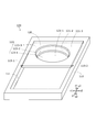
- FIG. 1 is a perspective view of a capacitive input device 100 (hereinafter sometimes referred to as the input device 100) according to the present embodiment.
- the input device 100 is mounted on a vehicle (not shown) and detects a position or movement touched by an external operation body (for example, a human finger, an operation pen).
- a control unit of a vehicle executes operations such as audio, air conditioning, and a navigation system in accordance with the position and movement of the external operating body.
- the x direction, the y direction, and the z direction orthogonal to each other are defined.
- the x direction is expressed without distinguishing the x1 direction and the x2 direction that are opposite to each other.
- the y direction represents the y1 direction and the y2 direction that are opposite to each other without distinction.
- the z direction represents the z1 direction and the z2 direction that are opposite to each other without distinction.
- the input device 100 includes a housing 110, a sensor substrate 120 supported by the housing 110, and a first rotation support member 115 that rotatably supports the sensor substrate 120 with respect to the housing 110. -1 and the second rotation support member 115-2 (hereinafter may be referred to as the rotation support member 115 without distinction), and a control device 140 that detects the coordinates of the external operation body with respect to the sensor substrate 120.
- FIG. 1 is a perspective view of the input device 100 when the sensor substrate 120 is in the first rotation position.
- FIG. 2 is a perspective view of the input device 100 when the sensor substrate 120 is in the second rotational position.
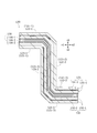
- FIG. 3 is a partial cutaway view of the sensor substrate 120 in a cross section passing through line 3-3 in FIG. 1 and parallel to the xz plane.
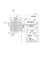
- FIG. 4 is a conceptual diagram of a control system of the input device 100.
- the housing 110 has a holding hole 111 opened in the z1 direction.
- the casing 110 is fixed to a vehicle (not shown).
- the shape of the housing 110 is an example.
- the sensor substrate 120 includes a first sensor unit 121-1, a second sensor unit 121-2, and a third sensor unit 121-3.
- the first sensor unit 121-1 is a disk-shaped part that extends substantially parallel to the xy plane (also referred to as a virtual plane).
- the second sensor unit 121-2 is a substantially cylindrical portion having a central axis along the z direction.
- the second sensor unit 121-2 extends from the periphery of the first sensor unit 121-1 in a direction intersecting the virtual plane (that is, the z2 direction).
- the third sensor unit 121-3 is a flat plate-like portion that extends in a direction away from the second sensor unit 121-2 substantially parallel to the virtual plane from the z2 side edge of the second sensor unit 121-2.
- the first rotation support member 115-1 protrudes in the x1 direction from the vicinity of the y2 side end portion in the x1 side end edge of the third sensor portion 121-3.
- the first rotation support member 115-1 extends in the x1 direction from the holding hole 111 of the housing 110 and extends into a hole provided in the housing 110.
- the second rotation support member 115-2 protrudes in the x2 direction from the vicinity of the y2 side end portion in the x2 side end edge of the third sensor portion 121-3.
- the second rotation support member 115-2 extends in the x2 direction from the holding hole 111 of the housing 110 and extends into a hole provided in the housing 110.
- the sensor substrate 120 is rotatable around the two rotation support members 115 between the first rotation position shown in FIG. 1 and the second rotation position shown in FIG.
- the second rotation position is a position where the sensor substrate 120 is rotated 180 degrees from the first rotation position. That is, at the second rotational position, the first sensor unit 121-1 and the third sensor unit 121-3 are substantially parallel to the xy plane.
- the sensor substrate 120 is fitted and fixed to the holding hole 111 at the first rotation position shown in FIG. 1 and the second rotation position shown in FIG.
- the sensor substrate 120 may be fixable at other rotational positions.
- the rotation support member 115 is an example, and may be another member that rotatably supports the sensor substrate 120, such as a hinge.
- the sensor substrate 120 has a first operation surface 122 exposed outside the holding hole 111 of the housing 110 (that is, operable from the z1 side) at the first rotation position.
- the first operation surface 122 includes a first surface 122-1 that is a surface on the z1 side of the first sensor unit 121-1 at the first rotational position and an outer side of the second sensor unit 121-2 at the first rotational position.
- a third surface 122-3 that is a surface on the z1 side of the third sensor part 121-3 at the first rotational position.
- the first surface 122-1 and the third surface 122-3 are substantially parallel to the xy plane.
- the second surface 122-2 is substantially cylindrical with a central axis in the z direction.
- the sensor substrate 120 has a second operation surface 123 exposed to the outside of the holding hole 111 of the housing 110 (that is, operable from the z1 side) at the second rotational position.
- the second operation surface 123 includes a first back surface 123-1 that is a surface on the z1 side of the first sensor unit 121-1 at the second rotational position, and an inner side of the second sensor unit 121-2 at the second rotational position.
- the second back surface 123-2 that is the surface of the third sensor portion 121 and the third back surface 123-3 that is the surface on the z1 side of the third sensor portion 121-3 at the second rotational position.
- the first back surface 123-1 and the third back surface 123-3 are substantially parallel to the xy plane.
- the second back surface 123-2 has a substantially cylindrical shape having a central axis in the z direction.
- the sensor substrate 120 has a shape protruding in the z1 direction from the third sensor unit 121-3 toward the first sensor unit 121-1 at the first rotational position. As shown in FIG. 2, the sensor substrate 120 has a shape that is recessed in the z2 direction from the third sensor unit 121-3 toward the first sensor unit 121-1 at the second rotational position.
- the sensor substrate 120 includes a sensor layer 130, a first cover layer 131, and a second cover layer 132.
- the sensor layer 130 is located between the first cover layer 131 and the second cover layer 132.
- the first cover layer 131 is laminated on the sensor layer 130 on the first operation surface 122 side.
- the second cover layer 132 is stacked on the second operation surface 123 side of the sensor layer 130.
- the sensor layer 130, the first cover layer 131, and the second cover layer 132 are all thin plate-like members that extend along the outer shape of the sensor substrate 120 shown in FIG.
- the two rotation support members 115 support the first cover layer 131, the second cover layer 132, and the sensor layer 130 so as to be integrally rotatable with respect to the housing 110.
- the sensor layer 130 includes a first electrode layer 130-1, a second electrode layer 130-2, and a dielectric base layer 130-3.
- the dielectric base layer 130-3 is located between the first electrode layer 130-1 and the second electrode layer 130-2.
- the first electrode layer 130-1, the second electrode layer 130-2, and the dielectric base layer 130-3 are all thin plate members that extend along the outer shape of the sensor substrate 120 shown in FIG.
- the dielectric base layer 130-3 is a thin plate member whose entire surface is formed of a dielectric.
- the first electrode layer 130-1 is laminated on the dielectric base layer 130-3 between the dielectric base layer 130-3 and the first cover layer 131.
- the second electrode layer 130-2 is laminated on the dielectric base layer 130-3 between the dielectric base layer 130-3 and the second cover layer 132.
- the first electrode layer 130-1 shown in FIG. 3 includes a plurality of first electrodes 150-1 shown in FIG. Each of the plurality of first electrodes 150-1 shown in FIG. 4 extends along the unevenness of the sensor substrate 120 shown in FIG. In the first electrode layer 130-1 shown in FIG. 3, the first electrodes 150-1 (FIG. 4) are insulated by a dielectric.
- the second electrode layer 130-2 shown in FIG. 3 includes a plurality of second electrodes 150-2 shown in FIG.
- Each of the plurality of second electrodes 150-2 shown in FIG. 4 extends along the unevenness of the sensor substrate 120 shown in FIG.
- the second electrodes 150-2 (FIG. 4) are insulated by a dielectric.
- a parasitic capacitor is formed at each intersection of the plurality of first electrodes 150-1 and the plurality of second electrodes 150-2. The capacitance of the capacitor formed at each crossing position decreases when an external operation body approaches from the first operation surface 122 side or when another external operation body approaches from the second operation surface 123 side.
- the plurality of first electrodes 150-1 and the plurality of second electrodes 150-2 shown in FIG. 4 may be referred to as electrodes 150 without being distinguished from each other.
- the electrodes 150 are conductive members each extending in a strip shape.
- the plurality of first electrodes 150-1 extend across the plurality of second electrodes 150-2. Since the plurality of first electrodes 150-1 and the plurality of second electrodes 150-2 are insulated by the dielectric base layer 130-3 (FIG. 3), they do not contact each other at the crossing positions.
- the intersection position of the plurality of first electrodes 150-1 and the plurality of second electrodes 150-2 is called a detection position 151. In FIG.
- one detection position 151 is representatively shown, but each of all the intersection positions is referred to as a detection position 151.
- a substantially constant capacitance is formed between the first electrode 150-1 and the second electrode 150-2.
- the capacitance at each detection position 151 is detected by the control device 140 described later.
- the electrostatic capacitance between the electrodes 150 is affected by the electrostatic capacitance between the electrode 150 and the external operating body, so that the detected electrostatic capacity changes.
- the plurality of electrodes 150 are depicted as extending in a planar shape. However, actually, the plurality of electrodes 150 are deformed along the unevenness of the sensor substrate 120 shown in FIG. A plurality of detection positions 151 shown in FIG. 4 are scattered in each of the first sensor unit 121-1, the second sensor unit 121-2, and the third sensor unit 121-3.
- the first cover layer 131 has the first operation surface 122 described above.
- the first cover layer 131 includes a first dielectric layer 131-1 positioned between the first operation surface 122 and the first electrode layer 130-1.
- the first dielectric layer 131-1 extends along the entire first electrode layer 130-1, and the plurality of first electrodes 150-1 (FIG. 4) in the first electrode layer 130-1 are subjected to the first operation. It is insulated from the external operating body on the surface 122 side.
- the first cover layer 131 includes a first shielding layer 131-2 formed of a conductive member inside the first dielectric layer 131-1.
- the first shielding layer 131-2 is located between a part of the first electrode 150-1 (FIG. 4) in the first electrode layer 130-1 and the first operation surface 122.
- the first shielding layer 131-2 does not cover the sensor layer 130 (that is, the plurality of electrodes 150 (FIG. 4)) at all on the first operation surface 122 side. Therefore, when the external operating body touches the second surface 122-2, the capacitance at the detection position 151 (FIG. 4) close to the touched position changes greatly. That is, the operation by the external operating body on the second surface 122-2 can be detected.
- the first shielding layer 131-2 may cover the sensor layer 130 with a part of the second sensor unit 121-2. In order to be able to detect the operation by the external operating body on the second surface 122-2, at least a part of the electrode 150 (FIG. 4) of the second sensor unit 121-2 is covered with the first shielding layer 131-2. It is sufficient if there is an undisclosed area.
- the first shielding layer 131-2 covers the entire sensor layer 130 (that is, the plurality of electrodes 150) in the first sensor unit 121-1 and the third sensor unit 121-3.
- the first shielding layer 131-2 is connected to the ground potential. Therefore, even if the external operating body touches either the first surface 122-1 or the third surface 122-3, the capacitance at the detection position 151 (FIG. 4) close to the touched position does not change. That is, the operation by the external operating body on the first surface 122-1 and the third surface 122-3 cannot be detected.
- the second cover layer 132 has the second operation surface 123 described above.
- the second cover layer 132 includes a second dielectric layer 132-1 positioned between the second operation surface 123 and the second electrode layer 130-2.
- the second dielectric layer 132-1 extends along the entire second electrode layer 130-2, and the plurality of second electrodes 150-2 (FIG. 4) in the second electrode layer 130-2 are second manipulated. It is insulated from the other external operation body on the surface 123 side.
- the second cover layer 132 includes a second shielding layer 132-2 formed of a conductive member inside the second dielectric layer 132-1.
- the second shielding layer 132-2 is located between a part of the second electrode 150-2 (FIG. 4) in the second electrode layer 130-2 and the second operation surface 123.
- the second shielding layer 132-2 does not cover the sensor layer 130 (that is, the plurality of electrodes 150 (FIG. 4)) at all on the second operation surface 123 side in the first sensor unit 121-1. Therefore, when the external operating body touches the first back surface 123-1, the capacitance at the detection position 151 (FIG. 4) close to the touched position changes greatly. That is, the operation by the external operating body on the first back surface 123-1 can be detected.
- the second shielding layer 132-2 may cover the sensor layer 130 with a part of the first sensor unit 121-1. In order to be able to detect an operation by the external operating body on the first back surface 123-1, at least a part of the electrode 150 (FIG. 4) of the first sensor unit 121-1 is covered with the second shielding layer 132-2. It is sufficient if there is an undisclosed area.
- the second shielding layer 132-2 covers the entire sensor layer 130 (that is, the plurality of electrodes 150 (FIG. 4)) in the second sensor unit 121-2 and the third sensor unit 121-3.
- the second shielding layer 132-2 is connected to the ground potential. Therefore, even if the external operating body touches either the second back surface 123-2 or the third back surface 123-3, the capacitance at the detection position 151 (FIG. 4) close to the touched position does not change. That is, the operation by the external operating body on the second back surface 123-2 and the third back surface 123-3 cannot be detected.
- the operation on the first front surface 122-1 cannot be detected, and the operation on the first back surface 123-1 can be detected.
- the operation on the second front surface 122-2 can be detected, and the operation on the second back surface 123-2 cannot be detected.
- the third sensor unit 121-3 an operation on any of the third front surface 122-3 and the third back surface 123-3 cannot be detected.
- the flat plate-like first cover layer 131 and the flat plate-like second cover layer 132 are laminated on the flat sensor layer 130. Next, it is formed by applying heat to the whole to be deformed.
- control device 140 includes a drive unit 141 that applies signals to the plurality of first electrodes 150-1, a detection unit 142 that detects signals on the plurality of second electrodes 150-2, and a memory.
- the storage device 143 stores the control program 145.
- the control program 145 is read by the arithmetic processing device 144 and causes the arithmetic processing device 144 to implement a function for performing a part of the control method of the input device 100 and other functions.
- the storage device 143 is controlled by the arithmetic processing device 144 and stores necessary information as appropriate.
- the storage device 143 is a non-temporary tangible storage medium.
- the storage device 143 includes a ROM (read only memory) and a RAM (random access memory).
- the storage device 143 is a volatile or nonvolatile storage medium.
- the storage device 143 may be removable or non-removable.
- the arithmetic processing unit 144 functions as a coordinate calculation unit 146 and a determination unit 147 described later by reading and executing the control program 145 stored in the storage device 143.
- the arithmetic processing unit 144 according to the present embodiment is a general-purpose computer, but may be an application specific integrated circuit (ASIC) and other functions capable of implementing each function described in the present embodiment. It may be a circuit.
- ASIC application specific integrated circuit
- the drive unit 141 applies a voltage to each of the plurality of first electrodes 150-1 according to the voltage pattern instructed from the coordinate calculation unit 146.
- the detection unit 142 detects a change in charge accumulated in a capacitor formed at each intersection position of the plurality of first electrodes 150-1 and the plurality of second electrodes 150-2, and outputs the change to the coordinate calculation unit 146. .
- the coordinate calculation unit 146 performs coordinate processing along the sensor layer 130 based on a change in capacitance of the capacitor formed at each intersection position of the plurality of first electrodes 150-1 and the plurality of second electrodes 150-2. As described above, the operation position of the external operation body on the first operation surface 122 side and the operation position of the other external operation body on the second operation surface 123 side are calculated. Specifically, the coordinate calculation unit 146 has a plurality of detection positions 151 based on voltage patterns applied to the plurality of first electrodes 150-1 and charges detected by the plurality of second electrodes 150-2. Detects changes in capacitance.
- the coordinate calculation unit 146 calculates, as the operation position, the coordinates at which the external operating body is close based on the change in capacitance.
- the coordinate calculation unit 146 makes no distinction as to which of the first operation surface 122 and the second operation surface 123 is close to the external operation body. Since the calculation method of the coordinate in an electrostatic capacitance type input device is well known, description is abbreviate
- the input device 100 of this embodiment is a mutual capacitance type, in another example, a self-capacitance type may be sufficient.
- the storage device 143 stores in advance coordinates corresponding to the first area and coordinates corresponding to the second area.
- the first region is a region where the sensor layer 130 shown in FIG. 3 is covered by the second shielding layer 132-2 and is not covered by the first shielding layer 131-2.
- the first region corresponds to the second sensor unit 121-2.
- the second region is a region where the sensor layer 130 shown in FIG. 3 is covered with the first shielding layer 131-2 and is not covered with the second shielding layer 132-2. That is, in FIG. 3, the second region corresponds to the first sensor unit 121-1.
- the determination unit 147 shown in FIG. 4 is based on the first operation surface 122 (FIG. 1) based on the coordinates of the operation position calculated by the coordinate calculation unit 146 and the first region and the second region stored in the storage device 143. ) Or the second operation surface 123 (FIG. 2).
- the determination unit 147 determines that an operation has been received from the first operation surface 122 (FIG. 1), and the operation position Is within the second region (ie, the first sensor unit 121-1 shown in FIG. 2), it is determined that an operation has been received from the second operation surface 123 (FIG. 2).
- the controller 140 changes the volume of the audio when a finger pinching the second surface 122-2 moves in the circumferential direction.
- the control device 140 recognizes a character based on the movement of the finger tracing the first back surface 123-1.
- the sensor layer 130 may have a region that is not covered by both the first shielding layer 131-2 and the second shielding layer 132-2. In the region that is not covered by both the first shielding layer 131-2 and the second shielding layer 132-2, the operations of both the first operation surface 122 and the second operation surface 123 are accepted without distinction.
- the sensor substrate 120 may have other shapes such as a flat plate, a rectangular parallelepiped, and a sphere.
- FIG. 5 is a flowchart for explaining a control method of the input device 100.
- the coordinate calculation unit 146 detects a change in capacitance at each of the detection positions 151 (FIG. 4) scattered on the sensor substrate 120 (FIG. 1).
- the operation position is detected.
- the coordinate calculation unit 146 (FIG. 4) does not distinguish between the first operation surface 122 (FIG. 1) and the second operation surface 123 (FIG. 2).
- the operation position refers to a position where the capacitance has changed greatly compared to the case where the external operation body is not in proximity among the plurality of detection positions 151 (FIG. 4).
- the operation position may be one detection position 151 (FIG. 4) or a plurality of detection positions 151 (FIG. 4).
- step 161 shown in FIG. 5 the determination unit 147 (FIG. 4) determines whether the operation position is in the first region (corresponding to the second sensor unit 121-2 shown in FIG. 1). If the determination unit 147 (FIG. 4) determines that the operation position is within the first region in step 161, the determination unit 147 (FIG. 4) determines that the operation is received from the first operation surface 122 (FIG. 1) in step 162, Exit.
- the second sensor unit 121-2 is covered with the second shielding layer 132-2 from the second operation surface 123 side. Therefore, even if the external operating body is close to the second operation unit 123 side second sensor unit 121-2, the capacitance does not change at the detection position 151 (FIG. 4) included in the second sensor unit 121-2.
- the second sensor unit 121-2 is not covered with the first shielding layer 131-2 from the first operation surface 122 side. Therefore, it can be understood that the operation in the second sensor unit 121-2 is an operation from the first operation surface 122 side.
- step 161 determines in step 161 shown in FIG. 5 that the operation position is not within the first region
- the process proceeds to step 163.
- step 163 the determination unit 147 (FIG. 4) determines whether the operation position is in the second region (corresponding to the first sensor unit 121-1 shown in FIG. 2). If the determination unit 147 (FIG. 4) determines that the operation position is within the second region in step 163, the determination unit 147 (FIG. 4) determines that the operation has been received from the second operation surface 123 (FIG. 2). End the method.
- the first sensor unit 121-1 is covered with the first shielding layer 131-2 from the first operation surface 122 side. Therefore, even if the external operating body approaches the first sensor unit 121-1 from the first operation surface 122 side, the capacitance does not change at the detection position 151 (FIG. 4) included in the first sensor unit 121-1. .
- the first sensor unit 121-1 is not covered with the second shielding layer 132-2 from the second operation surface 123 side. Therefore, it can be understood that the operation in the first sensor unit 121-1 is an operation from the second operation surface 123 side.
- step 163 shown in FIG. 5 the control method is terminated without specifying the surface on which the operation has been performed.
- a sensor including a plurality of electrodes 150 whose capacitance changes depending on the operation from the first operation surface 122 of the first cover layer 131 and the operation from the second operation surface 123 of the second cover layer 132. Since the layer 130 is located between the first cover layer 131 and the second cover layer 132, the size can be reduced as compared with the conventional one while realizing the double-sided operation.
- the first cover layer 131 includes the conductive first shielding layer 131-2 positioned between a part of the plurality of electrodes 150 and the first operation surface 122, and the first shielding layer 131-. 2 and the first dielectric layer 131-1 that insulates the plurality of electrodes 150 from each other, a change in capacitance occurs in a portion shielded by the first shielding layer 131-2 among the plurality of electrodes 150.
- the second operation surface 123 has been operated. That is, it can be easily determined from the operated position that the second operation surface 123 has been operated.
- the second cover layer 132 includes the conductive second shielding layer 132-2 positioned between a part of the plurality of electrodes 150 and the second operation surface 123, and the second shielding layer 132-. 2 and the second dielectric layer 132-1 that insulates the plurality of electrodes 150, the capacitance of the plurality of electrodes 150 is changed by the portion shielded by the second shielding layer 132-2.
- the first operation surface 122 has been operated. That is, it is possible to easily determine that the first operation surface 122 has been operated from the operated position.
- the coordinate calculation unit 146 detects the sensor based on the change in the capacitance of the capacitor formed at each intersection position of the plurality of first electrodes 150-1 and the plurality of second electrodes 150-2. Since the position of the external operation body on the first operation surface 122 side and the position of the other external operation body on the second operation surface 123 side are calculated as coordinates along the layer 130, the first operation surface 122 side and the first operation surface 122 side Compared to the case where separate electrodes 150 are used on the two operation surfaces 123 side, the size can be reduced.
- the first electrode layer 130-1 having the plurality of first electrodes 150-1 is laminated on the dielectric base layer 130-3 between the dielectric base layer 130-3 and the first cover layer 131.
- the second electrode layer 130-2 having the plurality of second electrodes 150-2 is laminated on the dielectric base layer 130-3 between the dielectric base layer 130-3 and the second cover layer 132.
- the space between the first operation surface 122 and the dielectric base layer 130-3, the second operation surface 123 side, and the dielectric base layer 130- It is easy to make a similar structure between the three and the position of the external operating body can be easily detected.
- the determination unit 147 determines that an operation has been received from the first operation surface 122 when the operation position is within the first region, and the second operation surface when the operation position is within the second region. 123, the operation from the first operation surface 122 and the operation from the second operation surface 123 can be easily performed only by detecting the coordinates even if there is no other member such as a mechanical switch. Can be identified.
- the plurality of electrodes 150 are entirely covered with the first shielding layer 131-2 in the first sensor unit 121-1, and the plurality of electrodes 150 are formed in the first sensor unit 121-1. At least a portion is not covered with the second shielding layer 132-2, and in the second sensor unit 121-2, the entirety of the plurality of electrodes 150 is covered with the second shielding layer 132-2.
- the two sensor unit 121-2 since at least a part of the plurality of electrodes 150 is not covered with the first shielding layer 131-2, only the operation from the second operation surface 123 is performed in the first sensor unit 121-1.
- the second sensor unit 121-2 can detect only the operation from the first operation surface 122. That is, the operable surface can be changed between the first sensor unit 121-1 and the second sensor unit 121-2.
- the rotation support member 115 includes the first cover layer 131, the second cover layer 132, and the sensor layer 130, the first rotation position where the first operation surface 122 is exposed to the outside, and the second operation surface. Since 123 is rotatably supported at the second rotation position exposed to the outside, the operation on the first operation surface 122 and the operation on the second operation surface 123 can be easily switched by the rotation operation.
- the present invention is applicable to, for example, a capacitive input device used for operation of a vehicle, a train, an aircraft, a ship, a spacecraft, and the like, and is used for operation of an electronic device such as a personal computer. Applicable to input devices.
- DESCRIPTION OF SYMBOLS 100 ... Input device, 110 ... Housing
Landscapes
- Engineering & Computer Science (AREA)
- General Engineering & Computer Science (AREA)
- Theoretical Computer Science (AREA)
- Human Computer Interaction (AREA)
- Physics & Mathematics (AREA)
- General Physics & Mathematics (AREA)
- Position Input By Displaying (AREA)
Abstract
静電容量式入力装置100は、第1操作面122をもつ第1カバー層131と、第2操作面123をもつ第2カバー層132と、第1カバー層131と第2カバー層132との間に位置するセンサ層130と、検出部142と、を備え、センサ層130が、第1操作面122側の外部操作体に対する位置と第2操作面123側の他の外部操作体に対する位置とに応じて静電容量が変わる複数の電極150を含み、第1カバー層131が、第1操作面122と複数の電極150とを絶縁しており、第2カバー層132が、第2操作面123と複数の電極150とを絶縁しており、検出部142が、複数の電極150における静電容量の変化を検出する。
Description
本発明は、静電容量式入力装置、静電容量式入力装置の制御方法、及び静電容量式入力装置の制御プログラムに関する。
操作面に対する人の指などの操作体の位置や動きを、操作面に近接配置された電極における静電容量の変化に基づいて判定する静電容量式入力装置がある。例えば、特許文献1に記載された入力装置は、複数の電極を搭載したセンサ基板を誘電体層で覆った構造をもつ。操作面として機能する誘電体層の外表面に人の指が触れると、接触位置付近の電極の静電容量が変化する。接触位置における静電容量の変化に基づいて、指の位置が操作面内の座標として計算される。操作面は平面だけではなく、特許文献1に記載のように凹面や凸面にすることもできる。
近年、入力装置の両面から入力操作することが求められている。特許文献1の入力装置では、センサ基板の片側にのみ操作面が設けられているので、両面から入力操作するには、2つの入力装置が必要である。特許文献2に記載の表示入力装置では、ディスプレイ基板を、片面にのみ操作面をもつ独立した2つの平板状の入力装置で挟むことにより、両面からの入力操作を実現している。
しかしながら、特許文献2の表示入力装置のように、2つの入力装置を使用して両面からの入力操作を実現すると、装置が大型化及び複雑化するという不利益がある。
本発明はかかる事情に鑑みてなされたものであり、その目的は、両面操作を実現しながら小型化できる静電容量式入力装置、静電容量式入力装置の制御方法、及び静電容量式入力装置の制御プログラムを提供することにある。
本発明は、第1操作面をもつ第1カバー層と、第2操作面をもつ第2カバー層と、第1カバー層と第2カバー層との間に位置するセンサ層と、検出部と、を備え、センサ層が、第1操作面側の外部操作体に対する位置と第2操作面側の他の外部操作体に対する位置とに応じて静電容量が変わる複数の電極を含み、第1カバー層が、外部操作体から複数の電極を絶縁しており、第2カバー層が、他の外部操作体から複数の電極を絶縁しており、検出部が、複数の電極における静電容量の変化を検出する、静電容量式入力装置である。
この構成によれば、第1カバー層の第1操作面からの操作と第2カバー層の第2操作面からの操作とにより静電容量が変化する電極を複数含んだセンサ層が第1カバー層と第2カバー層との間に位置するので、両面操作を実現しながら従来に比べて小型化できる。
好適には本発明の静電容量式入力装置において、第1カバー層が、複数の電極の一部と第1操作面との間に位置する導電性の第1遮蔽層と、第1遮蔽層と複数の電極とを絶縁する第1誘電体層と、を含む。
この構成によれば、第1カバー層が、複数の電極の一部と第1操作面との間に位置する導電性の第1遮蔽層と、第1遮蔽層と複数の電極とを絶縁する第1誘電体層とを含むので、複数の電極のうち第1遮蔽層に遮蔽された部分で静電容量の変化が生じた場合、第2操作面が操作されたことがわかる。すなわち、第2操作面が操作されたことを、操作された位置から簡単に判別することができる。
好適には本発明の静電容量式入力装置において、第2カバー層が、複数の電極の一部と第2操作面との間に位置する導電性の第2遮蔽層と、第2遮蔽層と複数の電極とを絶縁する第2誘電体層と、を含む。
この構成によれば、第2カバー層が、複数の電極の一部と第2操作面との間に位置する導電性の第2遮蔽層と、第2遮蔽層と複数の電極とを絶縁する第2誘電体層とを含むので、複数の電極のうち第2遮蔽層に遮蔽された部分で静電容量の変化が生じた場合、第1操作面が操作されたことがわかる。すなわち、第1操作面が操作されたことを、操作された位置から簡単に判別することができる。
好適には本発明の静電容量式入力装置において、座標算出部をさらに備え、複数の電極が、複数の第1電極と、複数の第2電極と、を有し、複数の第1電極の延びる方向と複数の第2電極の延びる方向とが交差し、座標算出部が、複数の第1電極と複数の第2電極との各交差位置に形成されるキャパシタの静電容量の変化に基づいて、センサ層に沿った座標として、外部操作体と他の外部操作体との操作位置を算出する。
この構成によれば、座標算出部が、複数の第1電極と複数の第2電極との各交差位置に形成されるキャパシタの静電容量の変化に基づいて、センサ層に沿った座標として、外部操作体の位置と他の外部操作体の位置とを算出するので、第1操作面側と第2操作面側とで別々の電極を使用する場合に比べて小型化できる。
好適には本発明の静電容量式入力装置において、センサ層が、誘電体基層と、誘電体基層と第1カバー層との間で誘電体基層上に積層された第1電極層と、誘電体基層と第2カバー層との間で誘電体基層上に積層された第2電極層と、を含み、第1電極層が、複数の第1電極を有し、第2電極層が、複数の第2電極を有する。
この構成によれば、誘電体基層と第1カバー層との間で誘電体基層上に複数の第1電極を有する第1電極層が積層され、誘電体基層と第2カバー層との間で誘電体基層上に複数の第2電極を有する第2電極層が積層されているので、誘電体基層の片側にすべての電極を配置する場合に比べて、第1操作面側と誘電体基層との間と、第2操作面側と誘電体基層との間とで類似した構造を作りやすく、外部操作体の位置の検出を簡単化できる。
好適には本発明の静電容量式入力装置において、第2遮蔽層に覆われ、かつ、第1遮蔽層に覆われていない第1領域に対応する座標と、第1遮蔽層に覆われ、かつ、第2遮蔽層に覆われていない第2領域に対応する座標とを記憶した記憶装置と、操作位置が第1領域内である場合、第1操作面から操作を受けたと判定し、操作位置が第2領域内である場合、第2操作面から操作を受けたと判定する判定部と、をさらに備える。
この構成によれば、判定部は、操作位置が第1領域内である場合、第1操作面から操作を受けたと判定し、操作位置が第2領域内である場合、第2操作面から操作を受けたと判定するので、機械スイッチ等の他の部材がなくても、座標を検出するだけで、簡単に第1操作面からの操作と第2操作面からの操作とを識別できる。
好適には本発明の静電容量式入力装置において、第1カバー層と第2カバー層とセンサ層とを含むセンサ基板を備え、センサ基板が、仮想平面に略平行に広がる第1センサ部と、第1センサ部の周縁から仮想平面に交差する方向に延びた第2センサ部と、を含み、第1カバー層が、複数の電極の一部と第1操作面との間に位置する導電性の第1遮蔽層と、第1遮蔽層と複数の電極とを絶縁する第1誘電体層と、を含み、第2カバー層が、複数の電極の一部と第2操作面との間に位置する導電性の第2遮蔽層と、第2遮蔽層と複数の電極とを絶縁する第2誘電体層と、を含み、第1センサ部において、複数の電極の全体が、第1遮蔽層に覆われており、第1センサ部において、複数の電極の少なくとも一部が、第2遮蔽層に覆われておらず、第2センサ部において、複数の電極の全体が、第2遮蔽層に覆われており、第2センサ部において、複数の電極の少なくとも一部が、第1遮蔽層に覆われていない。
この構成によれば、第1センサ部において、複数の電極の全体が、第1遮蔽層に覆われており、第1センサ部において、複数の電極の少なくとも一部が、第2遮蔽層に覆われておらず、第2センサ部において、複数の電極の全体が、第2遮蔽層に覆われており、第2センサ部において、複数の電極の少なくとも一部が、第1遮蔽層に覆われていないので、第1センサ部では第2操作面からの操作のみが検出可能となり、第2センサ部では第1操作面からの操作のみが検出可能となる。すなわち、第1センサ部と第2センサ部とで操作可能な面を変えることができる。
好適には本発明の静電容量式入力装置において、筐体と、第1カバー層と第2カバー層とセンサ層とを筐体に対して一体的に回転可能に支持する回転支持部材と、をさらに備え、回転支持部材が、第1カバー層と第2カバー層とセンサ層とを、第1操作面を外部に露出する第1回転位置と、第2操作面を外部に露出する第2回転位置とに回転可能に支持している。
この構成によれば、回転支持部材が、第1カバー層と第2カバー層とセンサ層とを、第1操作面を外部に露出する第1回転位置と、第2操作面を外部に露出する第2回転位置とに回転可能に支持するので、第1操作面に対する操作と第2操作面に対する操作とを、回転操作により簡単に切り替えることができる。
本発明は、第1操作面をもつ第1カバー層と、第2操作面をもつ第2カバー層と、第1カバー層と第2カバー層との間に位置するセンサ層と、検出部と、座標算出部とを備える静電容量式入力装置の制御方法であって、センサ層が、第1操作面側の外部操作体に対する位置と第2操作面側の他の外部操作体に対する位置とに応じて静電容量が変わる複数の電極を含み、第1カバー層が、外部操作体から複数の電極を絶縁しており、第2カバー層が、他の外部操作体から複数の電極を絶縁しており、検出部が、複数の電極における静電容量の変化を検出し、複数の電極が、複数の第1電極と、複数の第2電極と、を有し、複数の第1電極の延びる方向と複数の第2電極の延びる方向とが交差し、制御方法が、座標算出部により、複数の第1電極と複数の第2電極との各交差位置に形成されるキャパシタの静電容量の変化に基づいて、センサ層に沿った座標として、外部操作体と他の外部操作体との操作位置を算出することを含む、静電容量式入力装置の制御方法である。
本発明は、コンピュータに上記の制御方法を実行させる、静電容量式入力装置の制御プログラムである。
本発明によれば、両面操作を実現しながら小型化できる静電容量式入力装置、静電容量式入力装置の制御方法、及び静電容量式入力装置の制御プログラムを提供することができる。
以下、本発明の実施形態に係る静電容量式入力装置について説明する。図1は、本実施形態に係る静電容量式入力装置100(以下、入力装置100と呼ぶ場合がある。)の斜視図である。入力装置100は、図示しない車両に搭載されて、外部操作体(例えば、人間の指、操作用のペンなど)が触れた位置や動きを検出する。図示しない車両の制御部が、外部操作体の位置や動きに応じて、オーディオ、空調、ナビゲーションシステムなどの操作を実行する。
本明細書において、互いに直交するx方向、y方向、及びz方向を規定する。x方向は、互いに逆を向くx1方向とx2方向とを区別せずに表す。y方向は互いに逆を向くy1方向とy2方向とを区別せずに表す。z方向は互いに逆を向くz1方向とz2方向とを区別せずに表す。これらの方向は、相対的な位置関係を説明するために便宜上規定するのであって、実際の使用時の方向を限定するわけではない。構成要素の形状は、「略」という記載があるかないかにかかわらず、本明細書で開示された実施形態の技術思想が実現される限り、記載された表現に基づく厳密な幾何学的な形状に限定されない。
図1に示すように、入力装置100は、筐体110と、筐体110に支持されたセンサ基板120と、センサ基板120を筐体110に対して回転可能に支持する第1回転支持部材115-1及び第2回転支持部材115-2と(以下、区別せずに回転支持部材115と呼ぶ場合がある)、センサ基板120に対する外部操作体の座標を検出する制御装置140とを備える。図1は、センサ基板120が第1回転位置にあるときの入力装置100の斜視図である。図2は、センサ基板120が第2回転位置にあるときの入力装置100の斜視図である。図3は、図1の3-3線を通りxz平面に平行な断面におけるセンサ基板120の部分切断面図である。図4は、入力装置100の制御系統の概念図である。
(筐体)
図1に示すように、筐体110は、z1方向に開口した保持穴111をもつ。筐体110は、図示しない車両に固定される。筐体110の形状は、一例である。
図1に示すように、筐体110は、z1方向に開口した保持穴111をもつ。筐体110は、図示しない車両に固定される。筐体110の形状は、一例である。
(センサ基板)
図1を参照して、第1回転位置にあるセンサ基板120について説明する。センサ基板120は、第1センサ部121-1と第2センサ部121-2と第3センサ部121-3とを含む。第1センサ部121-1は、xy平面(仮想平面とも呼ばれる)に略平行に広がる円盤状の部位である。第2センサ部121-2は、z方向に沿った中心軸をもつ略円筒形の部位である。第2センサ部121-2は、第1センサ部121-1の周縁から、仮想平面に交差する方向(すなわち、z2方向)に延びている。第3センサ部121-3は、第2センサ部121-2のz2側の端縁から仮想平面に略平行に、第2センサ部121-2から離れる方向に広がる平板状の部位である。
図1を参照して、第1回転位置にあるセンサ基板120について説明する。センサ基板120は、第1センサ部121-1と第2センサ部121-2と第3センサ部121-3とを含む。第1センサ部121-1は、xy平面(仮想平面とも呼ばれる)に略平行に広がる円盤状の部位である。第2センサ部121-2は、z方向に沿った中心軸をもつ略円筒形の部位である。第2センサ部121-2は、第1センサ部121-1の周縁から、仮想平面に交差する方向(すなわち、z2方向)に延びている。第3センサ部121-3は、第2センサ部121-2のz2側の端縁から仮想平面に略平行に、第2センサ部121-2から離れる方向に広がる平板状の部位である。
(回転支持部材)
第1回転支持部材115-1は、第3センサ部121-3のx1側端縁内のy2側端部付近からx1方向に突出している。第1回転支持部材115-1は、筐体110の保持穴111内からx1方向に延びて、筐体110に設けた穴の中まで延びている。第2回転支持部材115-2は、第3センサ部121-3のx2側端縁内のy2側端部付近からx2方向に突出している。第2回転支持部材115-2は、筐体110の保持穴111内からx2方向に延びて、筐体110に設けた穴の中まで延びている。
第1回転支持部材115-1は、第3センサ部121-3のx1側端縁内のy2側端部付近からx1方向に突出している。第1回転支持部材115-1は、筐体110の保持穴111内からx1方向に延びて、筐体110に設けた穴の中まで延びている。第2回転支持部材115-2は、第3センサ部121-3のx2側端縁内のy2側端部付近からx2方向に突出している。第2回転支持部材115-2は、筐体110の保持穴111内からx2方向に延びて、筐体110に設けた穴の中まで延びている。
センサ基板120は、2つの回転支持部材115を中心として、図1に示す第1回転位置と図2に示す第2回転位置との間で回転可能である。第2回転位置は、センサ基板120が第1回転位置から180度回転した位置である。すなわち、第2回転位置において、第1センサ部121-1と第3センサ部121-3とが、xy平面に略平行となる。
本実施形態では、センサ基板120は、図1に示す第1回転位置と図2に示す第2回転位置とにおいて、保持穴111にはめ合わされて固定される。他の例において、センサ基板120は、他の回転位置に固定可能であってもよい。回転支持部材115は、例示であり、センサ基板120を回転可能に支持する他の部材、例えば、ヒンジなどであってもよい。
(センサ基板の操作面)
図1に示すように、センサ基板120は、第1回転位置において筐体110の保持穴111の外側に露出した(すなわち、z1側から操作可能な)第1操作面122をもつ。第1操作面122は、第1回転位置にある第1センサ部121-1のz1側の面である第1表面122-1と、第1回転位置にある第2センサ部121-2の外側の面である第2表面122-2と、第1回転位置にある第3センサ部121-3のz1側の面である第3表面122-3とを含む。第1表面122-1と第3表面122-3とは、xy平面に略平行である。第2表面122-2は、z方向に中心軸をもつ略円筒形である。
図1に示すように、センサ基板120は、第1回転位置において筐体110の保持穴111の外側に露出した(すなわち、z1側から操作可能な)第1操作面122をもつ。第1操作面122は、第1回転位置にある第1センサ部121-1のz1側の面である第1表面122-1と、第1回転位置にある第2センサ部121-2の外側の面である第2表面122-2と、第1回転位置にある第3センサ部121-3のz1側の面である第3表面122-3とを含む。第1表面122-1と第3表面122-3とは、xy平面に略平行である。第2表面122-2は、z方向に中心軸をもつ略円筒形である。
図2に示すように、センサ基板120は、第2回転位置において筐体110の保持穴111の外側に露出した(すなわち、z1側から操作可能な)第2操作面123をもつ。第2操作面123は、第2回転位置にある第1センサ部121-1のz1側の面である第1裏面123-1と、第2回転位置にある第2センサ部121-2の内側の面である第2裏面123-2と、第2回転位置にある第3センサ部121-3のz1側の面である第3裏面123-3とを含む。第1裏面123-1と第3裏面123-3とは、xy平面に略平行である。第2裏面123-2は、z方向に中心軸をもつ略円筒形である。
図1に示すように、センサ基板120は、第1回転位置において、第3センサ部121-3から第1センサ部121-1に向けてz1方向に突出した形状をもつ。図2に示すように、センサ基板120は、第2回転位置において、第3センサ部121-3から第1センサ部121-1に向けてz2方向に窪んだ形状をもつ。
(センサ基板の内部構造)
図3に示すように、センサ基板120は、センサ層130と第1カバー層131と第2カバー層132とを含む。センサ層130は、第1カバー層131と第2カバー層132との間に位置する。第1カバー層131は、センサ層130の第1操作面122側に積層されている。第2カバー層132は、センサ層130の第2操作面123側に積層されている。センサ層130と第1カバー層131と第2カバー層132とは、いずれも、図1に示すセンサ基板120の外形に沿って広がる薄板状の部材である。2つの回転支持部材115は、第1カバー層131と第2カバー層132とセンサ層130とを筐体110に対して一体的に回転可能に支持する。
図3に示すように、センサ基板120は、センサ層130と第1カバー層131と第2カバー層132とを含む。センサ層130は、第1カバー層131と第2カバー層132との間に位置する。第1カバー層131は、センサ層130の第1操作面122側に積層されている。第2カバー層132は、センサ層130の第2操作面123側に積層されている。センサ層130と第1カバー層131と第2カバー層132とは、いずれも、図1に示すセンサ基板120の外形に沿って広がる薄板状の部材である。2つの回転支持部材115は、第1カバー層131と第2カバー層132とセンサ層130とを筐体110に対して一体的に回転可能に支持する。
(センサ層)
図3に示すように、センサ層130は、第1電極層130-1と第2電極層130-2と誘電体基層130-3とを含む。誘電体基層130-3は、第1電極層130-1と第2電極層130-2との間に位置する。第1電極層130-1と第2電極層130-2と誘電体基層130-3とは、いずれも、図1に示すセンサ基板120の外形に沿って広がる薄板状の部材である。誘電体基層130-3は、全面が誘電体で形成された薄板状の部材である。第1電極層130-1は、誘電体基層130-3と第1カバー層131との間で誘電体基層130-3上に積層されている。第2電極層130-2は、誘電体基層130-3と第2カバー層132との間で誘電体基層130-3上に積層されている。
図3に示すように、センサ層130は、第1電極層130-1と第2電極層130-2と誘電体基層130-3とを含む。誘電体基層130-3は、第1電極層130-1と第2電極層130-2との間に位置する。第1電極層130-1と第2電極層130-2と誘電体基層130-3とは、いずれも、図1に示すセンサ基板120の外形に沿って広がる薄板状の部材である。誘電体基層130-3は、全面が誘電体で形成された薄板状の部材である。第1電極層130-1は、誘電体基層130-3と第1カバー層131との間で誘電体基層130-3上に積層されている。第2電極層130-2は、誘電体基層130-3と第2カバー層132との間で誘電体基層130-3上に積層されている。
図3に示す第1電極層130-1は、図4に示す複数の第1電極150-1を含む。図4に示す複数の第1電極150-1の各々は、図1に示すセンサ基板120の凹凸に沿って、互いに交わらずに概ねy方向に沿って延びている。図3に示す第1電極層130-1内において、第1電極150-1(図4)間は、誘電体で絶縁されている。
図3に示す第2電極層130-2は、図4に示す複数の第2電極150-2を含む。図4に示す複数の第2電極150-2の各々は、図1に示すセンサ基板120の凹凸に沿って、互いに交わらずに概ねx方向に沿って延びている。図3に示す第2電極層130-2内において、第2電極150-2(図4)間は、誘電体で絶縁されている。複数の第1電極150-1と複数の第2電極150-2との各交差位置には、寄生的なキャパシタが形成される。各交差位置に形成されるキャパシタの静電容量は、第1操作面122側から外部操作体が近づいた場合や、第2操作面123側から他の外部操作体が近づいた場合に小さくなる。
以下、図4に示す複数の第1電極150-1と複数の第2電極150-2とを区別せずに電極150と呼ぶ場合がある。電極150は、各々が帯状に延びた導電部材である。複数の第1電極150-1は、複数の第2電極150-2に交差して延びている。複数の第1電極150-1と複数の第2電極150-2とは、誘電体基層130-3(図3)により絶縁されているので交差位置で接触しない。複数の第1電極150-1と複数の第2電極150-2との交差位置は、検出位置151と呼ばれる。図4では1つの検出位置151を代表して示しているが、すべての交差位置の各々を検出位置151と呼ぶ。検出位置151の各々において、第1電極150-1と第2電極150-2との間に、略一定の静電容量が形成される。各検出位置151における静電容量は、後述の制御装置140により検出される。外部操作体が近づいた検出位置151では、電極150と外部操作体との静電容量により電極150間の静電容量が影響を受けるので、検出される静電容量が変化する。
図4では、簡略化して、複数の電極150が平面状に延びているように描かれている。しかし、実際には、複数の電極150は、図1に示すセンサ基板120の凹凸に沿って変形している。図4に示す検出位置151は、第1センサ部121-1と第2センサ部121-2と第3センサ部121-3との各々に複数点在している。
(第1カバー層)
図3に示すように、第1カバー層131は、前述の第1操作面122をもつ。第1カバー層131は、第1操作面122と第1電極層130-1との間に位置する第1誘電体層131-1を含む。第1誘電体層131-1は、第1電極層130-1の全体に沿って広がって、第1電極層130-1内の複数の第1電極150-1(図4)を第1操作面122側の外部操作体から絶縁している。第1カバー層131は、第1誘電体層131-1の内部に、導電性部材で形成された第1遮蔽層131-2を含む。第1遮蔽層131-2は、第1電極層130-1内の第1電極150-1(図4)の一部と第1操作面122との間に位置している。
図3に示すように、第1カバー層131は、前述の第1操作面122をもつ。第1カバー層131は、第1操作面122と第1電極層130-1との間に位置する第1誘電体層131-1を含む。第1誘電体層131-1は、第1電極層130-1の全体に沿って広がって、第1電極層130-1内の複数の第1電極150-1(図4)を第1操作面122側の外部操作体から絶縁している。第1カバー層131は、第1誘電体層131-1の内部に、導電性部材で形成された第1遮蔽層131-2を含む。第1遮蔽層131-2は、第1電極層130-1内の第1電極150-1(図4)の一部と第1操作面122との間に位置している。
第1遮蔽層131-2は、第2センサ部121-2では、第1操作面122側においてセンサ層130(すなわち、複数の電極150(図4))を全く覆っていない。従って、第2表面122-2に外部操作体が触れると、触れた位置に近い検出位置151(図4)の静電容量が大きく変化する。すなわち、第2表面122-2における外部操作体による操作が検出可能である。なお、他の例において、第1遮蔽層131-2は、第2センサ部121-2の一部でセンサ層130を覆っていてもよい。第2表面122-2における外部操作体による操作が検出可能であるためには、第2センサ部121-2の電極150(図4)の少なくとも一部に、第1遮蔽層131-2に覆われていない領域があればよい。
第1遮蔽層131-2は、第1センサ部121-1と第3センサ部121-3とにおいて、センサ層130(すなわち、複数の電極150)の全域を覆っている。第1遮蔽層131-2は、グランド電位に接続されている。従って、外部操作体が、第1表面122-1と第3表面122-3とのいずれに触れても、触れた位置に近い検出位置151(図4)の静電容量が変化しない。すなわち、第1表面122-1と第3表面122-3とにおける外部操作体による操作は検出不能である。
(第2カバー層)
図3に示すように、第2カバー層132は、前述の第2操作面123をもつ。第2カバー層132は、第2操作面123と第2電極層130-2との間に位置する第2誘電体層132-1を含む。第2誘電体層132-1は、第2電極層130-2の全体に沿って広がって、第2電極層130-2内の複数の第2電極150-2(図4)を第2操作面123側の他の外部操作体から絶縁している。第2カバー層132は、第2誘電体層132-1の内部に、導電性部材で形成された第2遮蔽層132-2を含む。第2遮蔽層132-2は、第2電極層130-2内の第2電極150-2(図4)の一部と第2操作面123との間に位置している。
図3に示すように、第2カバー層132は、前述の第2操作面123をもつ。第2カバー層132は、第2操作面123と第2電極層130-2との間に位置する第2誘電体層132-1を含む。第2誘電体層132-1は、第2電極層130-2の全体に沿って広がって、第2電極層130-2内の複数の第2電極150-2(図4)を第2操作面123側の他の外部操作体から絶縁している。第2カバー層132は、第2誘電体層132-1の内部に、導電性部材で形成された第2遮蔽層132-2を含む。第2遮蔽層132-2は、第2電極層130-2内の第2電極150-2(図4)の一部と第2操作面123との間に位置している。
第2遮蔽層132-2は、第1センサ部121-1では、第2操作面123側においてセンサ層130(すなわち、複数の電極150(図4))を全く覆っていない。従って、第1裏面123-1に外部操作体が触れると、触れた位置に近い検出位置151(図4)の静電容量が大きく変化する。すなわち、第1裏面123-1における外部操作体による操作が検出可能である。なお、他の例において、第2遮蔽層132-2は、第1センサ部121-1の一部でセンサ層130を覆っていてもよい。第1裏面123-1における外部操作体による操作が検出可能であるためには、第1センサ部121-1の電極150(図4)の少なくとも一部に、第2遮蔽層132-2に覆われていない領域があればよい。
第2遮蔽層132-2は、第2センサ部121-2と第3センサ部121-3とにおいて、センサ層130(すなわち、複数の電極150(図4))の全域を覆っている。第2遮蔽層132-2は、グランド電位に接続されている。従って、外部操作体が、第2裏面123-2と第3裏面123-3とのいずれに触れても、触れた位置に近い検出位置151(図4)の静電容量が変化しない。すなわち、第2裏面123-2と第3裏面123-3とにおける外部操作体による操作は検出不能である。
第1センサ部121-1では、第1表面122-1における操作は検出不能であり、第1裏面123-1における操作が検出可能である。第2センサ部121-2では、第2表面122-2における操作が検出可能であり、第2裏面123-2における操作が検出不能である。第3センサ部121-3では、第3表面122-3と第3裏面123-3とのいずれにおける操作も検出不能である。
例示的なセンサ基板120の製造工程では、まず、平板状に形成したセンサ層130に平板状の第1カバー層131と平板状の第2カバー層132が積層される。次に、全体に熱を加えて変形させることにより形成される。
(制御系統)
図4に示すように、制御装置140は、複数の第1電極150-1に信号を印加する駆動部141と、複数の第2電極150-2上の信号を検出する検出部142と、記憶装置143と演算処理装置144とを含む。
図4に示すように、制御装置140は、複数の第1電極150-1に信号を印加する駆動部141と、複数の第2電極150-2上の信号を検出する検出部142と、記憶装置143と演算処理装置144とを含む。
記憶装置143は、制御プログラム145を記憶する。制御プログラム145は、演算処理装置144によって読み出されて、演算処理装置144に入力装置100の制御方法の一部を行うための機能、及び他の機能を実装させる。演算処理装置144が種々の機能を実行するとき、記憶装置143は、演算処理装置144に制御されて、適宜必要な情報を記憶する。記憶装置143は、非一時的な有形の記憶媒体である。記憶装置143は、ROM(read only memory)及びRAM(random access memory)を含む。記憶装置143は、揮発性または不揮発性の記憶媒体である。記憶装置143は、取り外し可能であってもよく、取り外し不能であってもよい。
演算処理装置144は、記憶装置143に記憶された制御プログラム145を読み出して実行することにより、後述の座標算出部146と判定部147として機能する。本実施形態の演算処理装置144は、汎用コンピュータであるが、特定用途向け集積回路(ASIC;application specific integrated circuits)であってもよく、本実施形態で説明される各機能を実装可能な他の回路であってもよい。
駆動部141は、座標算出部146から指示された電圧パターンに従って、複数の第1電極150-1の各々に電圧を印加する。検出部142は、複数の第1電極150-1と複数の第2電極150-2との各交差位置に形成されるキャパシタに蓄積された電荷の変化を検出して座標算出部146に出力する。
座標算出部146は、複数の第1電極150-1と複数の第2電極150-2との各交差位置に形成されるキャパシタの静電容量の変化に基づいて、センサ層130に沿った座標として、第1操作面122側の外部操作体の操作位置と、第2操作面123側の他の外部操作体の操作位置とを算出する。具体的には、座標算出部146は、複数の第1電極150-1に印加する電圧パターンと、複数の第2電極150-2で検出された電荷とに基づいて、複数の検出位置151における静電容量の変化を検出する。
座標算出部146は、静電容量の変化に基づいて、外部操作体が近接した座標を操作位置として算出する。座標算出部146は、第1操作面122と第2操作面123とのいずれに外部操作体が近接したかについては区別しない。静電容量式入力装置における座標の算出方法はよく知られているので説明は省略する。なお、本実施形態の入力装置100は、相互容量式であるが、他の例において、自己容量式であってもよい。
記憶装置143には、予め、第1領域に対応する座標と第2領域に対応する座標とが記憶されている。第1領域は、図3に示すセンサ層130が第2遮蔽層132-2に覆われ、かつ、第1遮蔽層131-2に覆われていない領域である。図3では、第1領域は、第2センサ部121-2に対応する。第2領域は、図3に示すセンサ層130が第1遮蔽層131-2に覆われ、かつ、第2遮蔽層132-2に覆われていない領域である。すなわち、図3では、第2領域は、第1センサ部121-1に対応する。
図4に示す判定部147は、座標算出部146で算出された操作位置の座標と、記憶装置143に記憶された第1領域と第2領域とに基づいて、第1操作面122(図1)と第2操作面123(図2)とのいずれが操作を受けたのか判定する。判定部147は、操作位置が第1領域(すなわち、図1に示す第2センサ部121-2)内である場合、第1操作面122(図1)から操作を受けたと判定し、操作位置が第2領域(すなわち、図2に示す第1センサ部121-1)内である場合、第2操作面123(図2)から操作を受けたと判定する。
図1に示すようにセンサ基板120が第1回転位置にあるとき、外部に露出した第1操作面122のみが操作を受ける。第1操作面122のうち、略円筒形の第2センサ部121-2の第2表面122-2のみが、外部操作体による操作を検出する。例えば、制御装置140(図4)は、第2表面122-2をつまんだ指が周方向に動くと、オーディオのボリュームを変える。
図2に示すようにセンサ基板120が第2回転位置にあるとき、外部に露出した第2操作面123のみが操作を受ける。第2操作面123のうち、略円形の第1センサ部121-1の第1裏面123-1のみが、外部操作体による操作を検出する。例えば、制御装置140(図4)は、第1裏面123-1をなぞる指の動きに基づいて文字を認識する。
他の例において、センサ層130に、第1遮蔽層131-2と第2遮蔽層132-2との両方に覆われていない領域を有してもよい。第1遮蔽層131-2と第2遮蔽層132-2との両方に覆われていない領域では、第1操作面122と第2操作面123との両方の操作を区別せずに受け付ける。他の例において、センサ基板120は、平板、直方体、球など、他の形状であってもよい。
(制御方法)
図5は、入力装置100の制御方法を説明するためのフロー図である。
図5は、入力装置100の制御方法を説明するためのフロー図である。
まず、図5に示すステップ160において、座標算出部146(図4)は、センサ基板120(図1)上に点在する検出位置151(図4)の各々における静電容量の変化を検出することにより、操作位置を検出する。座標算出部146(図4)は、第1操作面122(図1)と第2操作面123(図2)とのいずれに外部操作体が近接したかについては区別しない。一例において、操作位置は、複数の検出位置151(図4)のうち、外部操作体が近接していない場合に比べて、静電容量が大きく変化した位置を指す。操作位置は、1つの検出位置151(図4)であってもよく、複数の検出位置151(図4)であってもよい。ステップ160が終わると、ステップ161に進む。
図5に示すステップ161において、判定部147(図4)は、操作位置が第1領域(図1に示す第2センサ部121-2に対応)内であるか判定する。判定部147(図4)は、ステップ161において操作位置が第1領域内であると判定した場合、ステップ162において、第1操作面122(図1)から操作を受けたと判定した後、制御方法を終了する。
図3に示すように、第2センサ部121-2は、第2操作面123側から、第2遮蔽層132-2に覆われている。そのため、外部操作体が第2操作面123側第2センサ部121-2に近接しても、第2センサ部121-2に含まれる検出位置151(図4)では静電容量が変化しない。一方、第2センサ部121-2は、第1操作面122側から、第1遮蔽層131-2に覆われていない。従って、第2センサ部121-2における操作は、第1操作面122側からの操作だとわかる。
判定部147(図4)は、図5に示すステップ161において、操作位置が第1領域内でないと判定した場合、処理をステップ163に進める。ステップ163において、判定部147(図4)は、操作位置が第2領域(図2に示す第1センサ部121-1に対応)内であるか判定する。判定部147(図4)は、ステップ163において、操作位置が第2領域内であると判定した場合、ステップ164において、第2操作面123(図2)から操作を受けたと判定した後、制御方法を終了する。
図3に示すように、第1センサ部121-1は、第1操作面122側から、第1遮蔽層131-2に覆われている。そのため、外部操作体が第1操作面122側から第1センサ部121-1に近接しても、第1センサ部121-1に含まれる検出位置151(図4)では静電容量が変化しない。一方、第1センサ部121-1は、第2操作面123側から、第2遮蔽層132-2に覆われていない。従って、第1センサ部121-1における操作は、第2操作面123側からの操作だとわかる。
判定部147(図4)は、図5に示すステップ163において、操作位置が第2領域内でないと判定した場合、操作を受けた面を特定せずに、制御方法を終了する。
(まとめ)
この構成によれば、第1カバー層131の第1操作面122からの操作と第2カバー層132の第2操作面123からの操作とにより静電容量が変化する電極150を複数含んだセンサ層130が第1カバー層131と第2カバー層132との間に位置するので、両面操作を実現しながら従来に比べて小型化できる。
この構成によれば、第1カバー層131の第1操作面122からの操作と第2カバー層132の第2操作面123からの操作とにより静電容量が変化する電極150を複数含んだセンサ層130が第1カバー層131と第2カバー層132との間に位置するので、両面操作を実現しながら従来に比べて小型化できる。
この構成によれば、第1カバー層131が、複数の電極150の一部と第1操作面122との間に位置する導電性の第1遮蔽層131-2と、第1遮蔽層131-2と複数の電極150とを絶縁する第1誘電体層131-1とを含むので、複数の電極150のうち第1遮蔽層131-2に遮蔽された部分で静電容量の変化が生じた場合、第2操作面123が操作されたことがわかる。すなわち、第2操作面123が操作されたことを、操作された位置から簡単に判別することができる。
この構成によれば、第2カバー層132が、複数の電極150の一部と第2操作面123との間に位置する導電性の第2遮蔽層132-2と、第2遮蔽層132-2と複数の電極150とを絶縁する第2誘電体層132-1とを含むので、複数の電極150のうち第2遮蔽層132-2に遮蔽された部分で静電容量の変化が生じた場合、第1操作面122が操作されたことがわかる。すなわち、第1操作面122が操作されたことを、操作された位置から簡単に判別することができる。
この構成によれば、座標算出部146が、複数の第1電極150-1と複数の第2電極150-2との各交差位置に形成されるキャパシタの静電容量の変化に基づいて、センサ層130に沿った座標として、第1操作面122側の外部操作体の位置と、第2操作面123側の他の外部操作体の位置とを算出するので、第1操作面122側と第2操作面123側とで別々の電極150を使用する場合に比べて小型化できる。
この構成によれば、誘電体基層130-3と第1カバー層131との間で誘電体基層130-3上に複数の第1電極150-1を有する第1電極層130-1が積層され、誘電体基層130-3と第2カバー層132との間で誘電体基層130-3上に複数の第2電極150-2を有する第2電極層130-2が積層されているので、誘電体基層130-3の片側にすべての電極150を配置する場合に比べて、第1操作面122側と誘電体基層130-3との間と、第2操作面123側と誘電体基層130-3との間とで類似した構造を作りやすく、外部操作体の位置の検出を簡単化できる。
この構成によれば、判定部147は、操作位置が第1領域内である場合、第1操作面122から操作を受けたと判定し、操作位置が第2領域内である場合、第2操作面123から操作を受けたと判定するので、機械スイッチ等の他の部材がなくても、座標を検出するだけで、簡単に第1操作面122からの操作と第2操作面123からの操作とを識別できる。
この構成によれば、第1センサ部121-1において、複数の電極150の全体が、第1遮蔽層131-2に覆われており、第1センサ部121-1において、複数の電極150の少なくとも一部が、第2遮蔽層132-2に覆われておらず、第2センサ部121-2において、複数の電極150の全体が、第2遮蔽層132-2に覆われており、第2センサ部121-2において、複数の電極150の少なくとも一部が、第1遮蔽層131-2に覆われていないので、第1センサ部121-1では第2操作面123からの操作のみが検出可能となり、第2センサ部121-2では第1操作面122からの操作のみが検出可能となる。すなわち、第1センサ部121-1と第2センサ部121-2とで操作可能な面を変えることができる。
この構成によれば、回転支持部材115が、第1カバー層131と第2カバー層132とセンサ層130とを、第1操作面122を外部に露出する第1回転位置と、第2操作面123を外部に露出する第2回転位置とに回転可能に支持するので、第1操作面122に対する操作と第2操作面123に対する操作とを、回転操作により簡単に切り替えることができる。
本発明は上述した実施形態には限定されない。すなわち、当業者は、本発明の技術的範囲またはその均等の範囲内において、上述した実施形態の構成要素に関し、様々な変更、コンビネーション、サブコンビネーション、並びに代替を行ってもよい。
本発明は、例えば、車両、列車、航空機、船舶、宇宙船などの操作に使用する静電容量式入力装置に適用可能であり、また、パソコンなどの電子機器の操作に使用する静電容量式入力装置に適用可能である。
100…入力装置、110…筐体
115…回転支持部材、115-1…第1回転支持部材、115-2…第2回転支持部材
120…センサ基板
121-1…第1センサ部、121-2…第2センサ部、121-3…第3センサ部
122…第1操作面、123…第2操作面、130…センサ層
130-1…第1電極層、130-2…第2電極層、130-3…誘電体基層
131…第1カバー層、131-1…第1誘電体層、131-2…第1遮蔽層
132…第2カバー層、132-1…第2誘電体層、132-2…第2遮蔽層
140…制御装置、142…検出部、143…記憶装置、145…制御プログラム
146…座標算出部、147…判定部
150…電極、150-1…第1電極、150-2…第2電極
115…回転支持部材、115-1…第1回転支持部材、115-2…第2回転支持部材
120…センサ基板
121-1…第1センサ部、121-2…第2センサ部、121-3…第3センサ部
122…第1操作面、123…第2操作面、130…センサ層
130-1…第1電極層、130-2…第2電極層、130-3…誘電体基層
131…第1カバー層、131-1…第1誘電体層、131-2…第1遮蔽層
132…第2カバー層、132-1…第2誘電体層、132-2…第2遮蔽層
140…制御装置、142…検出部、143…記憶装置、145…制御プログラム
146…座標算出部、147…判定部
150…電極、150-1…第1電極、150-2…第2電極
Claims (10)
- 第1操作面をもつ第1カバー層と、
第2操作面をもつ第2カバー層と、
前記第1カバー層と前記第2カバー層との間に位置するセンサ層と、
検出部と、
を備え、
前記センサ層が、前記第1操作面側の外部操作体に対する位置と前記第2操作面側の他の外部操作体に対する位置とに応じて静電容量が変わる複数の電極を含み、
前記第1カバー層が、前記外部操作体から前記複数の電極を絶縁しており、
前記第2カバー層が、前記他の外部操作体から前記複数の電極を絶縁しており、
前記検出部が、前記複数の電極における前記静電容量の変化を検出する、
静電容量式入力装置。 - 前記第1カバー層が、
前記複数の電極の一部と前記第1操作面との間に位置する導電性の第1遮蔽層と、
前記第1遮蔽層と前記複数の電極とを絶縁する第1誘電体層と、
を含む、
請求項1に記載の静電容量式入力装置。 - 前記第2カバー層が、
前記複数の電極の一部と前記第2操作面との間に位置する導電性の第2遮蔽層と、
前記第2遮蔽層と前記複数の電極とを絶縁する第2誘電体層と、
を含む、
請求項1または請求項2に記載の静電容量式入力装置。 - 座標算出部をさらに備え、
前記複数の電極が、
複数の第1電極と、
複数の第2電極と、を有し、
前記複数の第1電極の延びる方向と前記複数の第2電極の延びる方向とが交差し、
前記座標算出部が、前記複数の第1電極と前記複数の第2電極との各交差位置に形成されるキャパシタの静電容量の変化に基づいて、前記センサ層に沿った座標として、前記外部操作体と前記他の外部操作体との操作位置を算出する、
請求項1乃至請求項3の何れか一項に記載の静電容量式入力装置。 - 前記センサ層が、
誘電体基層と、
前記誘電体基層と前記第1カバー層との間で前記誘電体基層上に積層された第1電極層と、
前記誘電体基層と前記第2カバー層との間で前記誘電体基層上に積層された第2電極層と、
を含み、
前記第1電極層が、前記複数の第1電極を有し、
前記第2電極層が、前記複数の第2電極を有する、
請求項4に記載の静電容量式入力装置。 - 前記第2遮蔽層に覆われ、かつ、前記第1遮蔽層に覆われていない第1領域に対応する座標と、前記第1遮蔽層に覆われ、かつ、前記第2遮蔽層に覆われていない第2領域に対応する座標とを記憶した記憶装置と、
前記操作位置が前記第1領域内である場合、前記第1操作面から操作を受けたと判定し、前記操作位置が前記第2領域内である場合、前記第2操作面から操作を受けたと判定する判定部と、
をさらに備える、請求項4または請求項5に記載の静電容量式入力装置。 - 前記第1カバー層と前記第2カバー層と前記センサ層とを含むセンサ基板を備え、
前記センサ基板が、
仮想平面に略平行に広がる第1センサ部と、
前記第1センサ部の周縁から前記仮想平面に交差する方向に延びた第2センサ部と、
を含み、
前記第1カバー層が、
前記複数の電極の一部と前記第1操作面との間に位置する導電性の第1遮蔽層と、
前記第1遮蔽層と前記複数の電極とを絶縁する第1誘電体層と、
を含み、
前記第2カバー層が、
前記複数の電極の一部と前記第2操作面との間に位置する導電性の第2遮蔽層と、
前記第2遮蔽層と前記複数の電極とを絶縁する第2誘電体層と、
を含み、
前記第1センサ部において、前記複数の電極の全体が、前記第1遮蔽層に覆われており、
前記第1センサ部において、前記複数の電極の少なくとも一部が、前記第2遮蔽層に覆われておらず、
前記第2センサ部において、前記複数の電極の全体が、前記第2遮蔽層に覆われており、
前記第2センサ部において、前記複数の電極の少なくとも一部が、前記第1遮蔽層に覆われていない、
請求項1乃至請求項6の何れか一項に記載の静電容量式入力装置。 - 筐体と、
前記第1カバー層と前記第2カバー層と前記センサ層とを前記筐体に対して一体的に回転可能に支持する回転支持部材と、
をさらに備え、
前記回転支持部材が、前記第1カバー層と前記第2カバー層と前記センサ層とを、前記第1操作面を外部に露出する第1回転位置と、前記第2操作面を外部に露出する第2回転位置とに回転可能に支持している、
請求項1乃至請求項7の何れか一項に記載の静電容量式入力装置。 - 第1操作面をもつ第1カバー層と、第2操作面をもつ第2カバー層と、前記第1カバー層と前記第2カバー層との間に位置するセンサ層と、検出部と、座標算出部とを備える静電容量式入力装置の制御方法であって、
前記センサ層が、前記第1操作面側の外部操作体に対する位置と前記第2操作面側の他の外部操作体に対する位置とに応じて静電容量が変わる複数の電極を含み、
前記第1カバー層が、前記外部操作体から前記複数の電極を絶縁しており、
前記第2カバー層が、前記他の外部操作体から前記複数の電極を絶縁しており、
前記検出部が、前記複数の電極における前記静電容量の変化を検出し、
前記複数の電極が、
複数の第1電極と、
複数の第2電極と、を有し、
前記複数の第1電極の延びる方向と前記複数の第2電極の延びる方向とが交差し、
前記制御方法が、
前記座標算出部により、前記複数の第1電極と前記複数の第2電極との各交差位置に形成されるキャパシタの静電容量の変化に基づいて、前記センサ層に沿った座標として、前記外部操作体と前記他の外部操作体との操作位置を算出することを含む、
静電容量式入力装置の制御方法。 - コンピュータに請求項9に記載の制御方法を実行させる、静電容量式入力装置の制御プログラム。
Applications Claiming Priority (2)
| Application Number | Priority Date | Filing Date | Title |
|---|---|---|---|
| JP2016257149 | 2016-12-28 | ||
| JP2016-257149 | 2016-12-28 |
Publications (1)
| Publication Number | Publication Date |
|---|---|
| WO2018123471A1 true WO2018123471A1 (ja) | 2018-07-05 |
Family
ID=62711114
Family Applications (1)
| Application Number | Title | Priority Date | Filing Date |
|---|---|---|---|
| PCT/JP2017/043653 Ceased WO2018123471A1 (ja) | 2016-12-28 | 2017-12-05 | 静電容量式入力装置、静電容量式入力装置の制御方法、及び静電容量式入力装置の制御プログラム |
Country Status (1)
| Country | Link |
|---|---|
| WO (1) | WO2018123471A1 (ja) |
Citations (6)
| Publication number | Priority date | Publication date | Assignee | Title |
|---|---|---|---|---|
| JPH01102624A (ja) * | 1987-10-15 | 1989-04-20 | Canon Inc | 情報入出力装置 |
| JP2012174190A (ja) * | 2011-02-24 | 2012-09-10 | Japan Aviation Electronics Industry Ltd | 静電容量式タッチパネル及び画面入力装置 |
| JP2013080273A (ja) * | 2011-09-30 | 2013-05-02 | Sharp Corp | 表示入力装置及び表示方法 |
| WO2014174764A1 (ja) * | 2013-04-24 | 2014-10-30 | パナソニックIpマネジメント株式会社 | タッチパネル |
| WO2016031398A1 (ja) * | 2014-08-28 | 2016-03-03 | 富士フイルム株式会社 | 積層構造体およびタッチパネルモジュール |
| JP2016162312A (ja) * | 2015-03-03 | 2016-09-05 | ヤマハ株式会社 | パネル制御装置 |
-
2017
- 2017-12-05 WO PCT/JP2017/043653 patent/WO2018123471A1/ja not_active Ceased
Patent Citations (6)
| Publication number | Priority date | Publication date | Assignee | Title |
|---|---|---|---|---|
| JPH01102624A (ja) * | 1987-10-15 | 1989-04-20 | Canon Inc | 情報入出力装置 |
| JP2012174190A (ja) * | 2011-02-24 | 2012-09-10 | Japan Aviation Electronics Industry Ltd | 静電容量式タッチパネル及び画面入力装置 |
| JP2013080273A (ja) * | 2011-09-30 | 2013-05-02 | Sharp Corp | 表示入力装置及び表示方法 |
| WO2014174764A1 (ja) * | 2013-04-24 | 2014-10-30 | パナソニックIpマネジメント株式会社 | タッチパネル |
| WO2016031398A1 (ja) * | 2014-08-28 | 2016-03-03 | 富士フイルム株式会社 | 積層構造体およびタッチパネルモジュール |
| JP2016162312A (ja) * | 2015-03-03 | 2016-09-05 | ヤマハ株式会社 | パネル制御装置 |
Similar Documents
| Publication | Publication Date | Title |
|---|---|---|
| JP5123774B2 (ja) | 入力装置、及びそれを備えた表示装置 | |
| JP2009258888A (ja) | 入力装置、及びそれを備えた表示装置 | |
| US20140049271A1 (en) | Self-shielding co-planar touch sensor | |
| JP5781953B2 (ja) | 有効画面の境界部座標位置の取得が可能な静電容量式のタッチウインドウ及びその設計方法 | |
| US20150097801A1 (en) | Touch-sensor electrode details | |
| CN104076994B (zh) | 触摸位置感测面板 | |
| CN111164547A (zh) | 操作输入装置 | |
| US9436328B2 (en) | Single-layer touch sensor | |
| US20180307372A1 (en) | Touch Sensor and Associated Control Method for Decreased Capacitive Loads | |
| CN111538419B (zh) | 静电容式触摸面板的辅助输入工具 | |
| US20160349869A1 (en) | Self-capacitive touch panel and conductive layer structure thereof | |
| US20180253171A1 (en) | Touch detection | |
| US10635253B2 (en) | Pattern of electrodes for a touch sensor | |
| WO2018098771A1 (zh) | 确定方位角或姿态的方法、触控输入装置、触控屏及系统 | |
| WO2018123471A1 (ja) | 静電容量式入力装置、静電容量式入力装置の制御方法、及び静電容量式入力装置の制御プログラム | |
| US20140002369A1 (en) | Low impedance touch sensor | |
| TW201702814A (zh) | 包括具有用以促進追描之厚度之電極的裝置 | |
| JP2019506673A5 (ja) | ||
| US20180032182A1 (en) | Variable-Pitch Tracking For Touch Sensors | |
| US20140267141A1 (en) | Touch sensor with cover lens | |
| WO2019105050A1 (zh) | 一种触控显示面板和触控显示装置 | |
| US9354740B2 (en) | Object orientation determination | |
| WO2017134718A1 (ja) | タッチセンサ及びそれを備えた入力装置 | |
| WO2018012033A1 (ja) | 入力装置 | |
| JP7777384B2 (ja) | 入力装置 |
Legal Events
| Date | Code | Title | Description |
|---|---|---|---|
| 121 | Ep: the epo has been informed by wipo that ep was designated in this application |
Ref document number: 17887747 Country of ref document: EP Kind code of ref document: A1 |
|
| NENP | Non-entry into the national phase |
Ref country code: DE |
|
| 122 | Ep: pct application non-entry in european phase |
Ref document number: 17887747 Country of ref document: EP Kind code of ref document: A1 |
|
| NENP | Non-entry into the national phase |
Ref country code: JP |