WO2017188295A1 - 光変調器 - Google Patents
光変調器 Download PDFInfo
- Publication number
- WO2017188295A1 WO2017188295A1 PCT/JP2017/016471 JP2017016471W WO2017188295A1 WO 2017188295 A1 WO2017188295 A1 WO 2017188295A1 JP 2017016471 W JP2017016471 W JP 2017016471W WO 2017188295 A1 WO2017188295 A1 WO 2017188295A1
- Authority
- WO
- WIPO (PCT)
- Prior art keywords
- signal line
- optical modulator
- signal
- optical
- substrate
- Prior art date
- Legal status (The legal status is an assumption and is not a legal conclusion. Google has not performed a legal analysis and makes no representation as to the accuracy of the status listed.)
- Ceased
Links
Images




Classifications
-
- G—PHYSICS
- G02—OPTICS
- G02F—OPTICAL DEVICES OR ARRANGEMENTS FOR THE CONTROL OF LIGHT BY MODIFICATION OF THE OPTICAL PROPERTIES OF THE MEDIA OF THE ELEMENTS INVOLVED THEREIN; NON-LINEAR OPTICS; FREQUENCY-CHANGING OF LIGHT; OPTICAL LOGIC ELEMENTS; OPTICAL ANALOGUE/DIGITAL CONVERTERS
- G02F1/00—Devices or arrangements for the control of the intensity, colour, phase, polarisation or direction of light arriving from an independent light source, e.g. switching, gating or modulating; Non-linear optics
- G02F1/01—Devices or arrangements for the control of the intensity, colour, phase, polarisation or direction of light arriving from an independent light source, e.g. switching, gating or modulating; Non-linear optics for the control of the intensity, phase, polarisation or colour
- G02F1/03—Devices or arrangements for the control of the intensity, colour, phase, polarisation or direction of light arriving from an independent light source, e.g. switching, gating or modulating; Non-linear optics for the control of the intensity, phase, polarisation or colour based on ceramics or electro-optical crystals, e.g. exhibiting Pockels effect or Kerr effect
- G02F1/035—Devices or arrangements for the control of the intensity, colour, phase, polarisation or direction of light arriving from an independent light source, e.g. switching, gating or modulating; Non-linear optics for the control of the intensity, phase, polarisation or colour based on ceramics or electro-optical crystals, e.g. exhibiting Pockels effect or Kerr effect in an optical waveguide structure
Definitions
- the present invention relates to an optical modulator, and more particularly to a structure of a highly integrated modulator such as a two-wavelength integrated type.
- optical modulators used in optical communication systems are increasing in performance and density.
- miniaturization of substrates constituting the optical modulators is also being promoted.
- high performance, high density, and miniaturization of the optical modulator are contradictory requirements, a contrivance for achieving both of these is required.
- Patent Document 1 a first light modulation unit and a second light modulation unit are provided in parallel in the width direction on a substrate, and adjacent to one side of the substrate, an electric signal for modulation is provided.
- An optical modulator having a structure in which a relay substrate for relaying is disposed is disclosed.
- FIG. 1 shows an example of the configuration of an optical transmission apparatus including a conventional dual wavelength integrated DP-QPSK (Dual-Polarization--Quadrature-Phase-Shift-Keying) modulator.
- the optical modulator shown in the figure has an optical modulation region M1 to which an optical wave having a wavelength ⁇ 1 is input, and an optical modulation region M2 to which an optical wave having a wavelength ⁇ 2 different from the wavelength ⁇ 1 is input.
- M2 are configured to operate independently of each other.
- Each of the light modulation regions M1 and M2 propagates on the substrate 1 having the electro-optic effect, the optical waveguide 2, the control electrode 3 for controlling the light wave propagating through the optical waveguide 2 by the control signal, and the optical waveguide 2. And a light receiving element 4 for detecting a light wave to be detected.
- the control electrode 3 includes an RF electrode 3a to which an RF signal (modulation signal) that is a type of control signal is applied, or DC electrodes 3b and 3c to which a DC signal (bias voltage) that is a type of control signal is applied.
- the optical waveguide 2 in each of the light modulation regions M1 and M2 has a structure in which Mach-Zehnder type optical waveguides are arranged in a nested manner, and a large number of control electrodes 3 or light receiving elements 4 are provided accordingly. Yes.
- four RF electrodes 3a, six DC electrodes 3b and 3c, and two light receiving elements 4 are provided in each of the light modulation regions M1 and M2.
- a polarization beam combiner (not shown) is disposed downstream of the light modulation region M1, and the light wave propagating through the output side arm portion of the main Mach-Zehnder type optical waveguide is combined by the polarization beam combiner. Output to the optical fiber connected to. The same applies to the light modulation region M2.
- the polarization combining unit includes a structure that performs polarization combining using a spatial optical system or a structure that performs polarization combining using an optical waveguide.
- a high-frequency signal relay substrate 11 that relays an RF signal to the RF electrode 3a adjacent to the side of the substrate 1 on the light modulation region M2 side, and a DC signal for the DC electrodes 3b and 3c or light reception detected by the light receiving element 4.
- a relay board 12 for low frequency signals that relays signals is disposed.
- a termination substrate 13 for terminating an RF signal for the RF electrode 3a in the light modulation region M1 is disposed on the side of the substrate 1 on the light modulation region M1 side, and on the side of the substrate 1 on the light modulation region M2 side.
- a termination substrate 14 for terminating an RF signal for the RF electrode 3a in the light modulation region M2 is disposed.
- the optical modulator as described above is used by being incorporated in the optical transmission apparatus as one of the components constituting the optical transmission apparatus.
- an optical modulator is mounted on a printed circuit board 21 of an optical transmission device and operates based on a control signal from a driver element 22 disposed on the same surface as the mounting surface. That is, the optical modulator receives a control signal from the driver element 22 outside (outside the housing 6) and performs optical modulation according to the control signal.
- the driver element 22 is arranged in parallel to the side of the housing 6, the mounting area of the optical modulator and the driver element 22 becomes large, and it is difficult to reduce the size of the optical transmission device.
- RF connector or the like can be disposed on the same side surface of the housing 6. For this reason, there exists an advantage that it becomes easy to handle an optical modulator.
- a substrate (chip) on which a large number of control electrodes 3 (3a, 3b, 3c) or light receiving elements 4 are arranged the degree of freedom of wiring of signal lines (electric lines) connected to those components (3, 4) is high. Few.
- the length of the signal line with respect to the control electrode 3 tends to vary.
- variation in length occurs in each of the signal lines 5a and 5b with respect to the RF electrode 3a, thereby causing a skew (time delay) in the RF signal with respect to each RF electrode 3a or causing a difference in propagation loss between the signal lines.
- skew time delay
- the first problem to be solved by the present invention is to provide an optical modulator that solves the above problems and suppresses the variation in the length of the signal line with respect to the control electrode.
- the second problem to be solved by the present invention is to provide an optical transmission apparatus that solves the above-described problems and suppresses the mounting area of the optical modulator and the driver element.
- the optical modulator has the following technical features.
- a housing, two substrates having an electro-optic effect disposed inside the housing, and an optical waveguide formed on each of the two substrates and a light wave propagating through the optical waveguide are controlled by a control signal.
- An optical modulator having a control electrode for performing a relay substrate on which a relay signal line is formed between the two substrates, the control electrode and the relay signal line being electrically connected, and The control signal is input / output from one end of the relay signal line.
- a pin connected to one end of the relay signal line is disposed on the bottom surface outside the housing, and the control signal is input / output via the pin. It is characterized by being.
- control signal is a modulation signal of 20 Gbps or more.
- connection structure with the signal line outside the modulator on the side where the control signal of the pin is input is a connector.
- a flexible substrate on which a flexible signal line is formed is disposed on the bottom surface outside the housing, and one end of the flexible signal line is one end of the relay signal line And the control signal is input / output via the other end of the flexible signal line.
- control electrodes in the two substrates are arranged symmetrically with respect to a center line between the two substrates.
- the optical transmitter and the optical modulator have the following technical features.
- (B1) A housing, two substrates having an electro-optic effect disposed inside the housing, and an optical waveguide formed on each of the two substrates and a light wave propagating through the optical waveguide are controlled by a control signal.
- the driver element is disposed on the bottom side outside the casing, It is characterized by being connected.
- a relay substrate in which a relay signal line for electrically connecting the driver element and the control electrode is disposed between the two substrates. It is characterized by being.
- the driver element is disposed on a bottom surface outside the housing as viewed from a center line between the two substrates. It is characterized by.
- the driver element is configured such that a center line of the driver element matches a center line between the two boards when the two boards are viewed in a plan view. It is characterized by being arranged in.
- the driver element is disposed at a position overlapping the relay substrate when the two substrates are viewed in a plan view.
- control signal is 20 Gbps or more.
- the first aspect of the present invention it is possible to provide an optical modulator that suppresses variations in the length of the signal line with respect to the control electrode.
- the second aspect of the present invention it is possible to provide an optical transmission device in which the mounting area of the optical modulator and the driver element is suppressed.
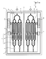
- the optical modulator to which the present invention is applied includes a housing 6, two substrates 1A and 1B having an electro-optic effect disposed inside the housing, and two substrates 1A and 1A. 1B, the optical waveguide 2 and the control electrode 3 for controlling the light wave propagating through the optical waveguide by a control signal.
- the substrates 1A and 1B may be any substrate that can form an optical waveguide such as quartz or semiconductor, and in particular, a substrate having an electrooptic effect, such as LiNbO 3 (lithium niobate), LiTaO 3 (lithium tantalate) or PLZT.
- a substrate using any single crystal of (lead lanthanum zirconate titanate) can be suitably used.
- the optical waveguide 2 formed on the substrates 1A and 1B is formed, for example, by thermally diffusing a high refractive index material such as titanium (Ti) on a LiNbO 3 substrate (LN substrate).
- a rib-type optical waveguide in which grooves are formed on both sides of a portion to be an optical waveguide or a ridge-type waveguide in which the optical waveguide portion is convex can be used.
- the present invention can also be applied to an optical circuit in which optical waveguides are formed on different waveguide substrates such as PLC and these waveguide substrates are bonded and integrated.
- the substrates 1A and 1B are provided with a control electrode 3 for controlling a light wave propagating through the optical waveguide 2 with a control signal.
- the control electrode 3 includes an RF electrode 3a constituting a modulation electrode, a ground electrode (not shown) surrounding the RF electrode 3a, and DC electrodes 3b and 3c for applying a DC signal.
- These control electrodes 3 can be formed by forming a Ti / Au electrode pattern on the substrate surface and using a gold plating method or the like.
- a buffer layer such as a dielectric SiO 2 can be provided on the substrate surface after the formation of the optical waveguide, if necessary.
- the optical waveguide 2 constituting each of the optical modulation regions of the substrates 1A and 1B has a structure in which Mach-Zehnder type waveguides are arranged in a nested manner, and a large number of control electrodes 3 or light receiving elements corresponding thereto. 4 is provided.
- four RF electrodes 3a, six DC electrodes 3b and 3c, and two light receiving elements 4 are provided on each of the substrates 1A and 1B.
- the length direction of the substrate is “X direction”
- the width direction of the substrate is “Y direction”
- the thickness direction of the substrate is “Z direction”.
- the X direction corresponds to the traveling direction of the light wave (the direction of the arrow X in the figure)
- the direction orthogonal to this is the Y direction
- the direction in which the substrate is viewed in plan is the Z direction.
- the main feature of the optical modulator according to one aspect of the present invention is that relay boards 11 and 12 each having a relay signal line (not shown) are disposed between the boards 1A and 1B, and the control electrode 3 and the relay signal are arranged. The lines are electrically connected, and the control signal is input / output from one end of the relay signal line.
- the first embodiment and the second embodiment will be described in detail.
- the schematic configuration of the optical modulator is the same as that of the conventional optical modulator described with reference to FIG.
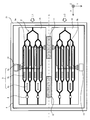
- FIG. 2 is a plan view for explaining an optical modulator according to the first embodiment of the present invention
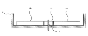
- FIG. 3 is a cross-sectional view taken along line AA ′ in FIG.
- the optical modulator of this example has two substrates 1A and 1B arranged in parallel in the Y direction on the inner bottom surface of the housing 6 (the surface inside the housing facing the bottom surface outside the housing). Between the substrate 1A and the substrate 1B, a high-frequency signal relay substrate 11 that relays an RF signal to the RF electrode 3a and a low-frequency signal relay substrate 12 that relays a DC signal to the DC electrodes 3b and 3c are arranged.
- the relay substrate 12 can also be used for relaying when a light reception signal detected by the light receiving element 4 is output to the outside.
- Relay signal lines are formed on the relay boards 11 and 12.
- One end of the relay signal line is electrically connected to the signal line for the control electrodes 3 of the substrates 1A and 1B, and the pin 7 is connected to the other end. That is, the relay signal line is electrically connected to the control electrode 3 and relays the control signal input / output from the pin 7 to / from the control electrode 3.
- the signal line 5a for the RF electrode 3a of the substrate 1A and the signal line 5b for the RF electrode 3a of the substrate 1B are shown, but the other signal lines are omitted.
- the signal lines are not concentrated locally as in the prior art. That is, it is not necessary to arrange a part of the signal line for the other light modulation region (M1) in one light modulation region (M2). Further, the length of the signal line can be adjusted by the way of arranging the relay signal line on the relay boards 11 and 12. For this reason, it becomes easy to arrange the length of the signal line, and the skew (phase shift) of the control signal due to the variation in the length of the signal line can be suppressed.
- the length of the signal line can be adjusted by the relay signal line on the relay boards 11 and 12, the propagation loss in the entire signal line can be reduced by shortening the signal line on the boards 1A and 1B having a large propagation loss as much as possible. And the occurrence of crosstalk between signal lines can be suppressed. Further, by forming a structure in which the chips are separated as in this example instead of forming a large number of light modulation regions on one substrate (chip), an effect of improving the yield of chip manufacture can be obtained.
- the relay signal lines formed on the relay boards 11 and 12 have pins extending from the relay boards 11 and 12 so as to penetrate the bottom surface of the housing 6 as shown in FIG.
- One end of 7 is electrically connected.
- the other end of the pin 7 is connected to a signal line outside the modulator for inputting and outputting control signals.
- the pin 7 may be used as it is.
- the structure on the other end side of the pin 7 may be a connector such as GPPO or G3PO.
- each control electrode 3 on the substrate 1A and each control electrode 3 on the substrate 1B are axisymmetric with respect to a center line between the substrates 1A and 1B (dashed line C in the figure). Is arranged. For this reason, even when a thermal stress is generated on the substrate 1A or the substrate 1B due to a temperature change outside or inside the optical modulator, the thermal stress on the substrate 1A or the substrate 1B is generated symmetrically with respect to the alternate long and short dash line C. Therefore, it is possible to suppress variations in optical characteristics or electrical characteristics between the substrate 1A and the substrate 1B.
- the relay boards 11 and 12 are not arranged on the same side of the inner wall side of the board 1A or the board 1B as in the prior art, the relay boards 11 and 12 are arranged between the board 1A and the board 1B. Combined with the above configuration, a synergistic effect can be obtained. Further, when the optical waveguides on the substrate 1A and the substrate 1B are also arranged symmetrically with respect to the alternate long and short dash line C, the above effect can be further enhanced.
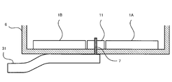
- FIG. 4 is a cross-sectional view for explaining an optical modulator according to the second embodiment of the present invention.
- a flexible substrate 31 on which a signal line (flexible signal line) is formed is arranged on the bottom surface side outside the housing 6.
- One end of a pin 7 extending from the relay boards 11 and 12 so as to penetrate the bottom surface of the housing 6 is electrically connected to the relay signal line formed on the relay boards 11 and 12.
- the other end of the pin 7 is electrically connected to one end of the flexible signal line.
- a control signal for the control electrode 3 is input / output from the other end of the flexible signal line.
- the propagation loss of the control signal can be reduced.
- the propagation loss can be reduced by increasing the proportion of sections formed by flexible signal lines in the signal path and minimizing the signal lines on the substrates 1A and 1B.
- wiring on the substrates 1A and 1B can be simplified, and design flexibility can be improved.
- DC signals and RF signals can be input / output from pins or connectors arranged on different surfaces of the housing.
- pins or connectors arranged on different surfaces of the housing are arranged so that the propagation direction of the DC signal and the propagation direction of the RF signal are orthogonal to each other in the portion connected to the signal line outside the modulator. It is good also as a structure.
- the propagation direction of the DC signal and the propagation direction of the RF signal are orthogonal to each other, so that crosstalk between the DC signal and the RF signal can be suppressed.
- the distance between the pin and the connector can be increased compared to the conventional configuration in which the pin and the connector are arranged on the same surface of the housing, the propagation direction of the DC signal and the propagation direction of the RF signal are orthogonal Due to the synergistic effect, crosstalk between the DC signal and the RF signal can be effectively suppressed.
- pins or connectors are arranged on the bottom and side surfaces of the housing, DC signals are input / output from pins or connectors arranged on the side surfaces of the housing, and RF signals are pins arranged on the bottom surface of the housing.
- the length of the signal line of the RF signal can be shortened, and effects such as reduction in skew, variation in propagation loss between signal lines, and reduction in propagation loss as a total of signal lines can be obtained.
- the effect of the present invention can be obtained even when the modulation signal is less than 20 Gbps. However, when the modulation signal is 20 Gbps or more, the suppression of propagation loss in the entire signal line and the suppression of occurrence of crosstalk between signal lines. With this, even higher effects can be achieved.
- the fixed surface of the substrate 1A, 1B or the relay substrate 11, 12 with the surface inside the housing may not be the entire surface of the substrate or the relay substrate.
- the substrates 1A and 1B or the relay substrates 11 and 12 arranged inside the housing may be fixed to the inner surface of the housing with an adhesive or solder, or the substrate or the relay substrate and the inner surface of the housing. You may fix via another member between.
- a main feature of the optical transmission device is that the driver element 22 that outputs a control signal to the control electrode 3 is arranged on the bottom surface side outside the housing of the optical modulator.
- the third embodiment and the fourth embodiment will be described in detail.
- the schematic configuration of the optical modulator and the optical transmitter is the same as that of the conventional optical modulator described with reference to FIG.
- FIG. 2 is a plan view for explaining an optical transmission apparatus according to a third embodiment of the present invention
- FIG. 5 is a sectional view of the optical transmission apparatus as viewed in the X direction.
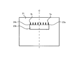
- FIG. 6 is a bottom view for explaining the arrangement of the driver elements 22.
- 5A is a diagram illustrating a state before the optical modulator is mounted on the printed circuit board of the optical transmission device
- FIG. 5B illustrates a state after the optical modulator is mounted on the printed circuit board of the optical transmission device.
- FIG. FIG. 6A is a diagram illustrating an example of the arrangement of driver elements
- FIG. 6B is a diagram illustrating another example of the arrangement of driver elements.
- the optical modulator in the optical transmitter of this example has two substrates 1A and 1B arranged in parallel in the Y direction on the inner bottom surface of the housing 6 (the surface inside the housing facing the bottom surface outside the housing). is there. Between the substrate 1A and the substrate 1B, a high-frequency signal relay substrate 11 that relays an RF signal to the RF electrode 3a and a low-frequency signal relay substrate 12 that relays a DC signal to the DC electrodes 3b and 3c are arranged.
- the relay substrate 12 can also be used for relaying when a light reception signal detected by the light receiving element 4 is output to the outside.
- the optical modulator of this example is used by being incorporated in the optical transmission device as one of the components constituting the optical transmission device.
- the optical modulator of this example is mounted on the printed circuit board 21 of the optical transmitter, and is controlled from the driver element 22 disposed on the surface (lower surface) opposite to the mounting surface (upper surface). Operates based on the signal. That is, the driver element 22 that outputs a control signal is arranged on the bottom surface side outside the housing of the optical modulator.
- Relay signal lines are formed on the relay boards 11 and 12.
- One end of the relay signal line is electrically connected to the signal line for the control electrodes 3 of the substrates 1A and 1B, and the other end is electrically connected to pins 7a and 7b which are examples of electrical connection means.
- the pins 7 a and 7 b are formed so as to penetrate the bottom surface of the housing 6 from the relay boards 11 and 12. Further, the pins 7 a and 7 b are configured such that the length of the portion protruding from the bottom surface of the housing 6 is at least the thickness of the printed circuit board 21.
- the printed circuit board 21 is formed with through holes 23a and 23b through which the pins 7a and 7b can be inserted at positions where the pins 7a and 7b are located when the optical modulator is mounted. Further, output terminals 24 a and 24 b extending from the driver element 22 toward the through holes 23 a and 23 b are provided on the lower surface of the printed circuit board 21. When the optical modulator is mounted on the printed board 21, a part of the pins 7 a and 7 b protrude from the through holes 23 a and 23 b of the printed board 21.
- the relay signal lines of the relay boards 11 and 12 and the output terminals 24a and 24b of the printed board 21 can be electrically connected.
- the interval between the output terminals 24a, 24b and the through holes 23a, 23b is widened, and a signal line is formed between the output terminals 24a, 24b and the through holes 23a, 23b, and the pins 7a, 7b are connected via the signal lines.
- the output terminals 24a and 24b may be electrically connected.
- the output terminal 24a is a terminal for outputting a control signal supplied from the driver element 22 to the substrate 1A side.
- the output terminal 24b is a terminal for outputting a control signal supplied from the driver element 22 to the substrate 1B side. That is, for example, an RF signal for the substrate 1A is transmitted from the driver element 22 to the RF electrode 3a on the substrate 1A side through the output terminal 24a, the pin 7a, the signal line 5a, and the like. Also, for example, an RF signal for the substrate 1B is transmitted from the driver element 22 to the RF electrode 3b on the substrate 1B side through the output terminal 24b, the pin 7b, the signal line 5b, and the like. In FIG. 2, the signal line 5a for the RF electrode 3a of the substrate 1A and the signal line 5b for the RF electrode 3a of the substrate 1B are shown, but other signal lines are omitted.
- the driver element 22 is arranged on the bottom side outside the optical modulator housing, so that the size of the printed circuit board 21 can be reduced as compared with the conventional configuration. Thereby, it is possible to provide an optical transmission device in which the mounting area of the optical modulator and the driver element 22 is suppressed.
- the relay signal line for electrically connecting the driver element 22 and the control electrode 3 is formed on the relay substrates 11 and 12 disposed between the substrate 1A and the substrate 1B.
- the relay substrates 11 and 12 disposed between the substrate 1A and the substrate 1B.
- the length of the signal line can be adjusted by the relay signal line on the relay boards 11 and 12 or the signal line on the printed board 21. For this reason, by shortening the signal lines on the substrates 1A and 1B having a large propagation loss as much as possible, the propagation loss in the entire signal line can be suppressed, and the occurrence of crosstalk between the signal lines can be suppressed. Furthermore, instead of forming a large number of light modulation regions on a single substrate (chip), a structure in which the chips are separated as in this example can be achieved. For this reason, since the fine pattern of the waveguide or electrode mounted on one chip is reduced, an effect of improving the yield of chip manufacture due to a defect of a putter or the like can be obtained.
- the optical transmission device of this example at a position where it can be connected to the driver element 22 arranged on the bottom side outside the housing as seen from the center line (the one-dot chain line C in the figure) between the substrate 1A and the substrate 1B, Pins 7a and 7b are provided. For this reason, the length of the signal line from the driver element 22 to the control electrode 3 can be shortened efficiently. Thereby, the further reduction of the propagation loss of a control signal is realizable.
- the driver is positioned at a position where the center of the driver element 22 and the center line C meet when viewed in the Z direction as shown in FIG. 5 or 6A. You may comprise so that the element 22 may be arrange
- the center of the driver element 22 and the center line C are aligned in the Z direction as described above.
- the driver element 22 may be arranged at a position shifted from the center line C toward the substrate 1A or the substrate 1B.
- the relay boards 11 and 12 on one side of the printed board 7 and the driver element on the other side of the printed board 7 It is good also as a shift amount arrange
- control signal output terminals 24a and 24b are arranged on the left and right, an output terminal 24a extending to the through hole 23a on the substrate 1A side, and an output terminal 24b extending to the through hole 23b on the substrate 1B side.
- the output terminals 24a and 24b are arranged only on one side of the driver element 22 as shown in FIG. 6B, the output terminal 24a extending to the through hole 23a on the substrate 1A side and the through hole 23b on the substrate 1B side are similarly provided.
- the extending output terminal 24b may be arranged symmetrically with respect to the center line C.
- the arrangement of the output terminals 24a and 24b with respect to the driver element 22 can be similarly adopted in a fourth embodiment described later.
- the structure in which the driver element 22 is arranged on the bottom surface outside the housing may be applied when the control signal is 20 Gbps or more.
- FIG. 7 is a cross-sectional view for explaining an optical transmission apparatus according to the fourth embodiment of the present invention
- FIG. 8 is a cross-sectional view of the optical transmission apparatus viewed in the X direction.
- the optical modulator in the optical transmitter of this example has two substrates 1A and 1B arranged in parallel in the Y direction on the inner bottom surface of the housing 6 (the surface inside the housing facing the bottom surface outside the housing). is there.
- a high-frequency signal relay substrate 11A for the substrate 1A is disposed adjacent to the substrate 1A.
- a high-frequency signal relay substrate 11B for the substrate 1B is disposed adjacent to the substrate 1B.
- the optical modulator of this example is also used as one of the components constituting the optical transmission device.
- the optical modulator of this example is mounted on the printed circuit board 21 of the optical transmitter, and is controlled from the driver element 22 disposed on the surface (lower surface) opposite to the mounting surface (upper surface). Operates based on the signal. That is, the driver element 2 that outputs a control signal is arranged on the bottom surface side outside the housing of the optical modulator.
- the low-frequency signal relay board is not shown, like the high-frequency signal relay board, the side of the board 1A opposite to the board 1B and the board 1A of the board 1B are the same. It may be provided individually on both sides of the opposite side, or a common relay board may be provided only on one side.
- the driver element 22 can be disposed on the bottom surface outside the housing of the optical modulator, so that it is possible to provide an optical transmission device that reduces the mounting area of the optical modulator and the driver element 22. Further, as in the third embodiment, avoiding local concentration of the signal line, suppression of control signal skew (phase shift) due to variations in the length of the signal line, improvement of propagation loss in the entire signal line, etc. An effect can also be obtained.
- the first aspect of the present invention it is possible to provide an optical modulator that suppresses variations in the length of the signal line with respect to the control electrode.
- the second aspect of the present invention it is possible to provide an optical transmission device in which the mounting area of the optical modulator and the driver element is suppressed.
Landscapes
- Physics & Mathematics (AREA)
- Nonlinear Science (AREA)
- Chemical & Material Sciences (AREA)
- Engineering & Computer Science (AREA)
- Ceramic Engineering (AREA)
- Crystallography & Structural Chemistry (AREA)
- General Physics & Mathematics (AREA)
- Optics & Photonics (AREA)
- Optical Modulation, Optical Deflection, Nonlinear Optics, Optical Demodulation, Optical Logic Elements (AREA)
Abstract
制御電極に対する信号線路の長さのバラツキを抑えた光変調器を提供する。 光変調器は、筐体6と、該筐体内部に配置される電気光学効果を有する2つの基板1A,1Bと、2つの基板1A,1Bにそれぞれ形成された、光導波路2及び該光導波路を伝搬する光波を制御信号により制御するための制御電極3とを有する。2つの基板1A,1Bの間には中継信号線路(不図示)が形成された中継基板11,12が配置され、制御電極3と中継信号線路は電気的に接続され、制御信号は中継信号線路の一端から入出力される。
Description
本発明は、光変調器に関し、特に、2波長集積型などの高集積型変調器の構造に関する。
光通信システムの高速化、大容量化が進む中で、光通信システムに使用される光変調器の高性能化、高密度化が進んでいる。また、光変調器の小型化の要請に伴い、光変調器を構成する基板の小型化も進められている。しかしながら、光変調器の高性能化と、高密度化及び小型化とは相反する要求であるので、これらを両立するための工夫が求められている。
このような光変調器に関し、以下のような発明が提案されている。
例えば、特許文献1には、基板上に第1の光変調部と第2の光変調部とを幅方向に並列に設け、該基板の一方の側部に隣接させて、変調用の電気信号を中継する中継基板を配置した構造の光変調器が開示されている。
例えば、特許文献1には、基板上に第1の光変調部と第2の光変調部とを幅方向に並列に設け、該基板の一方の側部に隣接させて、変調用の電気信号を中継する中継基板を配置した構造の光変調器が開示されている。
近年、2波長集積型などの高集積型光変調器が開発されている。図1には、従来の2波長集積型DP-QPSK(Dual Polarization - Quadrature Phase Shift Keying)変調器を備えた光送信装置の構成例を示してある。同図の光変調器は、波長λ1の光波が入力される光変調領域M1と、波長λ1とは異なる波長λ2の光波が入力される光変調領域M2とを有し、これら光変調領域M1,M2は互いに独立して動作するように構成される。
光変調領域M1,M2の各々は、電気光学効果を有する基板1上に、光導波路2と、光導波路2を伝搬する光波を制御信号により制御するための制御電極3と、光導波路2を伝搬する光波を検出するための受光素子4とを備えている。制御電極3は、制御信号の一種であるRF信号(変調信号)が印加されるRF電極3a又は制御信号の一種であるDC信号(バイアス電圧)が印加されるDC電極3b,3cなどで構成される。
各光変調領域M1,M2の光導波路2は、マッハツェンダー型光導波路を入れ子型に多重に配置した構造となっており、これに相応して多数の制御電極3又は受光素子4が設けられている。同図では、光変調領域M1,M2のそれぞれに、4つのRF電極3aと、6つのDC電極3b,3cと、2つの受光素子4を設けてある。
光変調領域M1の下流には偏波合成部(不図示)が配置され、メインとなるマッハツェンダー型光導波路の出力側アーム部を伝搬する光波を偏波合成部で合成して、光変調器に接続された光ファイバに出力する。光変調領域M2についても同様である。偏波合成部は、空間光学系を用いて偏波合成を行う構造のもの又は光導波路を用いて偏波合成を行う構造のものなどがある。
光変調領域M1の下流には偏波合成部(不図示)が配置され、メインとなるマッハツェンダー型光導波路の出力側アーム部を伝搬する光波を偏波合成部で合成して、光変調器に接続された光ファイバに出力する。光変調領域M2についても同様である。偏波合成部は、空間光学系を用いて偏波合成を行う構造のもの又は光導波路を用いて偏波合成を行う構造のものなどがある。
基板1の光変調領域M2側の辺部に隣接させて、RF電極3aに対するRF信号を中継する高周波信号用の中継基板11と、DC電極3b,3cに対するDC信号又は受光素子4で検出した受光信号を中継する低周波信号用の中継基板12が配置されている。また、基板1の光変調領域M1側の辺部には、光変調領域M1のRF電極3aに対するRF信号を終端する終端基板13が配置され、基板1の光変調領域M2側の辺部には、光変調領域M2のRF電極3aに対するRF信号を終端する終端基板14が配置されている。
上記のような光変調器は、光送信装置を構成する部品の一つとして該光送信装置に内蔵して使用される。一般的に、光変調器は光送信装置のプリント基板21に搭載され、その搭載面と同一面上に配置されたドライバ素子22からの制御信号に基づいて動作する。すなわち、光変調器は、その外部(筐体6の外部)にあるドライバ素子22から制御信号の供給を受けて、制御信号に応じた光変調を行う。しかしながら、ドライバ素子22が筐体6の側方に並列させて配置する構造だと、光変調器及びドライバ素子22の実装面積が大きくなるので、光送信装置の小型化が困難であった。
また、上記のように基板1の片側に中継基板11,12を配置する構造だと、高周波信号用の中継基板11又は低周波信号用の中継基板12に接続される入出力端子(DCピン又はRFコネクタなど)を筐体6の同一な側面に配置することができる。このため、光変調器を取り扱いやすくなるという利点がある。しかしながら、多数の制御電極3(3a,3b,3c)又は受光素子4を配置した基板(チップ)では、それらの部品(3,4)に接続する信号線路(電気線)の配線の自由度が少ない。特に中継基板11,12に近い側の光変調領域M2は、光変調領域M2に対する信号線路だけでなく、光変調領域M1に対する信号線路の一部も配設されるとともに、信号線路が局所的に集中することになるので、信号線路の複雑化が顕著になる。その結果、制御電極3(3a,3b,3c)に対する信号線路の長さにバラツキが生じやすい。例えば、RF電極3aに対する信号線路5a,5bの各々で長さにバラツキが生じることで、各RF電極3aに対するRF信号にスキュー(時間遅延)が発生したり、各々の信号線路で伝搬損失差が生じる懸念がある。また、信号線路の長さが長くなると伝搬損失が増加したり、信号線路間でクロストークが発生する可能性があるという問題もある。
本発明が解決しようとする第1の課題は、上記のような問題を解決し、制御電極に対する信号線路の長さのバラツキを抑えた光変調器を提供することである。また、本発明が解決しようとする第2の課題は、上記のような問題を解決し、光変調器及びドライバ素子の実装面積を抑えた光送信装置を提供することである。
上記第1の課題を解決するため、第1の本発明では、光変調器は、以下のような技術的特徴を有する。
(A1) 筐体と、該筐体内部に配置される電気光学効果を有する2つの基板と、前記2つの基板にそれぞれ形成された、光導波路及び該光導波路を伝搬する光波を制御信号により制御するための制御電極とを有する光変調器において、前記2つの基板の間には中継信号線路が形成された中継基板が配置され、該制御電極と該中継信号線路は電気的に接続され、該制御信号は該中継信号線路の一端から入出力されることを特徴とする。
(A1) 筐体と、該筐体内部に配置される電気光学効果を有する2つの基板と、前記2つの基板にそれぞれ形成された、光導波路及び該光導波路を伝搬する光波を制御信号により制御するための制御電極とを有する光変調器において、前記2つの基板の間には中継信号線路が形成された中継基板が配置され、該制御電極と該中継信号線路は電気的に接続され、該制御信号は該中継信号線路の一端から入出力されることを特徴とする。
(A2) 上記(A1)に記載の光変調器において、該筐体外部の底面には該中継信号線路の一端に接続されたピンが配置され、該制御信号は、該ピンを介して入出力されることを特徴とする。
(A3) 上記(A2)に記載の光変調器において、該制御信号は20Gbps以上の変調信号であることを特徴とする。
(A4) 上記(A2)又は(A3)に記載の光変調器において、該ピンの制御信号が入力される側における変調器外部の信号線路との接続構造はコネクタであることを特徴とする。
(A5) 上記(A1)に記載の光変調器において、該筐体外部の底面側にはフレキシブル信号線路が形成されたフレキシブル基板が配置され、該フレキシブル信号線路の一端は該中継信号線路の一端に接続され、該制御信号は該フレキシブル信号線路の他端を介して入出力されることを特徴とする。
(A6) 上記(A5)に記載の光変調器において、該制御信号のスキューの調整は該フレキシブル基板に配置された該フレキシブル信号線路で行うことを特徴とする。
(A7) 上記(A1)乃至(A6)のいずれかに記載の光変調器において、前記2つの基板における該制御電極は前記2つの基板間の中心線に対して線対称に配置されることを特徴とする。
上記第2の課題を解決するため、第2の本発明では、光送信装置及び光変調器は、以下のような技術的特徴を有する。
(B1) 筐体と、該筐体内部に配置される電気光学効果を有する2つの基板と、前記2つの基板にそれぞれ形成された、光導波路及び該光導波路を伝搬する光波を制御信号により制御するための制御電極とを有する光変調器と、該制御信号を出力するドライバ素子とを備えた光送信装置において、該ドライバ素子は該筐体外部の底面側に配置され、該制御電極と電気的に接続されることを特徴とする。
(B1) 筐体と、該筐体内部に配置される電気光学効果を有する2つの基板と、前記2つの基板にそれぞれ形成された、光導波路及び該光導波路を伝搬する光波を制御信号により制御するための制御電極とを有する光変調器と、該制御信号を出力するドライバ素子とを備えた光送信装置において、該ドライバ素子は該筐体外部の底面側に配置され、該制御電極と電気的に接続されることを特徴とする。
(B2) 上記(B1)に記載の光送信装置において、前記2つの基板の間に、該ドライバ素子と該制御電極とを電気的に接続するための中継信号線路が形成された中継基板が配置されることを特徴とする。
(B3) 上記(B1)に記載の光送信装置において、前記2つの基板のそれぞれにおいて、前記2つの基板の間とは反対側に、該ドライバ素子と該制御電極とを電気的に接続するための中継信号線路が形成された中継基板が配置されることを特徴とする。
(B4) 上記(B1)乃至(B3)のいずれかに記載の光送信装置において、該ドライバ素子は、前記2つの基板間の中心線から見て該筐体外部の底面側に配置されることを特徴とする。
(B5) 上記(B4)に記載の光送信装置において、該ドライバ素子は、前記2つの基板を平面視する方向から見て該ドライバ素子の中心と前記2つの基板間の中心線とが合うように配置されることを特徴とする。
(B6) 上記(B2)に記載の光送信装置において、該ドライバ素子は、前記2つの基板を平面視する方向から見て該中継基板と重なる位置に配置されることを特徴とする。
(B7) 上記(B1)乃至(B6)のいずれかに記載の光送信装置において、該制御信号は20Gbps以上であることを特徴とする。
(B8) 外部のドライバ素子から出力される制御信号に基づいて動作する光変調器において、筐体と、該筐体内部に配置される電気光学効果を有する2つの基板と、前記2つの基板にそれぞれ形成された、光導波路及び該光導波路を伝搬する光波を該制御信号により制御するための制御電極と、該筐体外部の底面側に配置される該ドライバ素子を該制御電極と電気的に接続するための電気的接続手段とを備えたことを特徴とする。
第1の本発明によれば、制御電極に対する信号線路の長さのバラツキを抑えた光変調器を提供することができる。また、第2の本発明によれば、光変調器及びドライバ素子の実装面積を抑えた光送信装置を提供することができる。
以下、本発明に係る光変調器及び光送信装置について詳細に説明する。
本発明が適用される光変調器は、例えば図2に示すように、筐体6と、該筐体内部に配置される電気光学効果を有する2つの基板1A,1Bと、2つの基板1A,1Bにそれぞれ形成された、光導波路2及び該光導波路を伝搬する光波を制御信号により制御するための制御電極3とを有する。
本発明が適用される光変調器は、例えば図2に示すように、筐体6と、該筐体内部に配置される電気光学効果を有する2つの基板1A,1Bと、2つの基板1A,1Bにそれぞれ形成された、光導波路2及び該光導波路を伝搬する光波を制御信号により制御するための制御電極3とを有する。
基板1A,1Bとしては、石英、半導体など光導波路を形成できる基板であれば良く、特に、電気光学効果を有する基板である、LiNbO3(ニオブ酸リチウム),LiTaO3(タンタル酸リチウム)又はPLZT(ジルコン酸チタン酸鉛ランタン)のいずれかの単結晶などを用いた基板が好適に利用可能である。
基板1A,1Bに形成する光導波路2は、例えば、LiNbO3基板(LN基板)上にチタン(Ti)などの高屈折率物質を熱拡散することにより形成される。また、光導波路となる部分の両側に溝を形成したリブ型光導波路又は光導波路部分を凸状としたリッジ型導波路も利用可能である。また、PLC等の異なる導波路基板に光導波路を形成し、これらの導波路基板を貼り合せ集積した光回路にも、本発明を適用することが可能である。
基板1A,1Bには、光導波路2を伝搬する光波を制御信号により制御するための制御電極3が設けられる。制御電極3としては、変調電極を構成するRF電極3a及びこれを取り巻く接地電極(不図示)、DC信号を印加するDC電極3b、3cなどがある。これら制御電極3は、基板表面に、Ti・Auの電極パターンを形成し、金メッキ方法などにより形成することが可能である。さらに、必要に応じて光導波路形成後の基板表面に誘電体SiO2等のバッファ層を設けることも可能である。
基板1A,1Bの各々の光変調領域を構成する光導波路2は、マッハツェンダー型導波路を入れ子型に多重に配置した構造となっており、これに相応して多数の制御電極3又は受光素子4が設けられている。同図では、基板1A,1Bのそれぞれに、4つのRF電極3aと、6つのDC電極3b,3cと、2つの受光素子4を設けてある。
本明細書では、基板の長さ方向を「X方向」とし、基板の幅方向を「Y方向」とし、基板の厚さ方向を「Z方向」とする。X方向は光波の進行方向(図中の矢印Xの方向)に対応し、これに直交する方向(図中の矢印Yの方向)がY方向となり、基板を平面視する方向(図中の×印Zの方向)がZ方向となる。
(第1の本発明について)
本発明の一態様に係る光変調器の主な特徴は、基板1A,1Bの間に、中継信号線路(不図示)が形成された中継基板11,12が配置され、制御電極3と中継信号線路は電気的に接続され、制御信号は中継信号線路の一端から入出力されることである。以下、第1実施例及び第2実施例を参照して詳細に説明する。なお、光変調器の概略的な構成は、図1を参照して説明した従来の光変調器と同様である。
本発明の一態様に係る光変調器の主な特徴は、基板1A,1Bの間に、中継信号線路(不図示)が形成された中継基板11,12が配置され、制御電極3と中継信号線路は電気的に接続され、制御信号は中継信号線路の一端から入出力されることである。以下、第1実施例及び第2実施例を参照して詳細に説明する。なお、光変調器の概略的な構成は、図1を参照して説明した従来の光変調器と同様である。
図2は、本発明の第1実施例に係る光変調器を説明する平面図であり、図3は、図2におけるA-A’断面図である。
本例の光変調器は、筐体6の内部底面(筐体外部の底面に対向する筐体内部の面)に、2つの基板1A,1BをY方向に並列に配置してある。基板1Aと基板1Bの間には、RF電極3aに対するRF信号を中継する高周波信号用の中継基板11と、DC電極3b,3cに対するDC信号を中継する低周波信号用の中継基板12が配置される。中継基板12は、受光素子4で検出した受光信号を外部に出力する際の中継に用いることもできる。
本例の光変調器は、筐体6の内部底面(筐体外部の底面に対向する筐体内部の面)に、2つの基板1A,1BをY方向に並列に配置してある。基板1Aと基板1Bの間には、RF電極3aに対するRF信号を中継する高周波信号用の中継基板11と、DC電極3b,3cに対するDC信号を中継する低周波信号用の中継基板12が配置される。中継基板12は、受光素子4で検出した受光信号を外部に出力する際の中継に用いることもできる。
中継基板11,12には中継信号線路(不図示)が形成されている。中継信号線路は、一方の端部が基板1A,1Bの制御電極3に対する信号線路と電気的に接続され、他方の端部にピン7が接続される。すなわち、中継信号線路は、制御電極3と電気的に接続され、ピン7から入出力される制御信号を制御電極3との間で中継する。図2では、基板1AのRF電極3aに対する信号線路5aと、基板1BのRF電極3aに対する信号線路5bを示しているが、他の信号線路は省略している。
このように、基板1Aと基板1Bの間に、これらの基板に対する制御信号を中継する中継基板11,12を配置することで、従来技術のように信号線路が局所的に集中することがなくなる。すなわち、一方の光変調領域(M2)に、他方の光変調領域(M1)に対する信号線路の一部を配設させずに済むようになる。また、信号線路の長さは、中継基板11,12上の中継信号線路の配設の仕方により調整できる。このため、信号線路の長さを揃えやすくなり、信号線路の長さのバラツキによる制御信号のスキュー(位相ずれ)を抑制できる。
また、信号線路の長さの調整は中継基板11,12上の中継信号線路で行えるので、伝搬損失が大きい基板1A,1B上の信号線路をなるべく短くすることで、信号線路全体での伝搬損失を抑え、また信号線路間でクロストークの発生を抑制することが可能となる。更に、1枚の基板(チップ)に多数の光変調領域を形成するのではなく、本例のようにチップを分離した構造にすることで、チップ製造の歩留りを改善する効果も得られる。
また、本例の光変調器において、中継基板11,12に形成された中継信号線路には、図3に示すように、中継基板11,12から筐体6の底面を貫通するように延びるピン7の一端が電気的に接続されている。ピン7の他端は制御信号の入出力のため変調器外部の信号線路と接続される。ピン7の他端側(制御信号が入力される側)における変調器外部の信号線路との接続構造としては、制御信号がDC信号の場合、ピン7をそのまま利用してもよい。また制御信号がRF信号の場合、ピン7の他端側における当該構造はGPPO又はG3POなどのコネクタとしてもよい。
このように、筐体6の底面から出たピン7を介して制御信号を入出力する構成とすることで、ピン7の他端から制御電極3に至る信号線路の長さを短縮できる。その結果、スキューの低減、信号線路間の伝搬損失のバラツキの低減、信号線路トータルとしての伝搬損失の低減といった効果を得ることができる。
また、本例の光変調器は、基板1Aにおける各制御電極3と基板1Bにおける各制御電極3を、基板1Aと基板1Bの間の中心線(図中の一点鎖線C)に対して線対称に配置している。このため、光変調器外部もしくは内部の温度変化により基板1A又は基板1Bに熱応力が発生した場合でも、基板1A又は基板1Bに対する熱応力が一点鎖線Cに対して対称に発生する。したがって、基板1Aと基板1B間の光学特性又は電気特性の劣化のバラつきを抑制することができる。また、従来のように中継基板11,12を基板1Aもしくは基板1Bの筐体内壁側の同じ側面に配置せず、基板1Aと基板1Bの間に中継基板11,12を配置しているので、上記構成と相俟って相乗的な効果を得ることができる。また、基板1A及び基板1Bにおける光導波路も一点鎖線Cに対して対称に配置した場合、更に上記効果を高めることができる。
図4は、本発明の第2実施例に係る光変調器を説明する断面図である。
本例の光変調器は、筐体6の外部の底面側に、信号線路(フレキシブル信号線路)が形成されたフレキシブル基板31を配置してある。中継基板11,12に形成された中継信号線路には、中継基板11,12から筐体6の底面を貫通するように延びるピン7の一端が電気的に接続されている。また、ピン7の他端はフレキシブル信号線路の一端と電気的に接続されている。制御電極3に対する制御信号は、フレキシブル信号線路の他端から入出力される。
本例の光変調器は、筐体6の外部の底面側に、信号線路(フレキシブル信号線路)が形成されたフレキシブル基板31を配置してある。中継基板11,12に形成された中継信号線路には、中継基板11,12から筐体6の底面を貫通するように延びるピン7の一端が電気的に接続されている。また、ピン7の他端はフレキシブル信号線路の一端と電気的に接続されている。制御電極3に対する制御信号は、フレキシブル信号線路の他端から入出力される。
このように、制御電極3に対する制御信号の信号経路の一部を、基板1A又は基板1Bなどより伝搬損失が小さいフレキシブル信号線路で形成することで、制御信号の伝搬損失を低減することができる。特に、信号経路においてフレキシブル信号線路で形成する区間の割合を多くし、基板1A,1B上の信号線路を最小限に抑えることで、信号線路トータルとしての伝搬損失を低減することができる。また、スキューの調整を、配線取り回しが容易なフレキシブル信号線路の区間で行うことで、基板1A,1B上の配線を簡素化でき、設計自由度の改善を図ることができる。
以上、第1の本発明について、第1実施例及び第2実施例を用いて説明したが、本発明は上述した内容に限定されず、本発明の趣旨を逸脱しない範囲で適宜設計変更可能であることはいうまでもない。
一例として、DC信号とRF信号を、筐体の互いに異なる面に配置されたピン又はコネクタからそれぞれ入出力する構成とすることができる。
この場合、例えば、筐体の互いに異なる面に配置されたピン又はコネクタは、変調器外部の信号線路と接続される部分におけるDC信号の伝搬方向とRF信号の伝搬方向が直交するように配置する構成としてもよい。こうすることで、DC信号の伝搬方向とRF信号の伝搬方向が直交するので、DC信号とRF信号との間のクロストークが抑制できる。また、筐体の同一面にピンとコネクタを配置した従来の構成と比較して、ピンとコネクタの距離を大きくすることができるので、DC信号の伝搬方向とRF信号の伝搬方向が直交することとの相乗効果により、DC信号とRF信号との間のクロストークを効果的に抑制することができる。
一例として、DC信号とRF信号を、筐体の互いに異なる面に配置されたピン又はコネクタからそれぞれ入出力する構成とすることができる。
この場合、例えば、筐体の互いに異なる面に配置されたピン又はコネクタは、変調器外部の信号線路と接続される部分におけるDC信号の伝搬方向とRF信号の伝搬方向が直交するように配置する構成としてもよい。こうすることで、DC信号の伝搬方向とRF信号の伝搬方向が直交するので、DC信号とRF信号との間のクロストークが抑制できる。また、筐体の同一面にピンとコネクタを配置した従来の構成と比較して、ピンとコネクタの距離を大きくすることができるので、DC信号の伝搬方向とRF信号の伝搬方向が直交することとの相乗効果により、DC信号とRF信号との間のクロストークを効果的に抑制することができる。
また、例えば、筐体の底面と側面にピン又はコネクタをそれぞれ配置し、DC信号は筐体の側面に配置されたピン又はコネクタから入出力し、RF信号は筐体の底面に配置されたピン又はコネクタから入出力する構成としてもよい。このような構成の場合でも、RF信号の信号線路の長さを短縮することができ、スキューの低減、信号線路間の伝搬損失のバラツキの低減、信号線路トータルとしての伝搬損失の低減といった効果を得ることができる。
尚、本発明の効果は変調信号が20Gbps未満でも一定の効果が得られるが、変調信号が20Gbps以上の場合、信号線路全体での伝搬損失の抑制及び信号線路間でクロストーク発生の抑制の面で更に高い効果を奏することができる。
尚、本発明の効果は変調信号が20Gbps未満でも一定の効果が得られるが、変調信号が20Gbps以上の場合、信号線路全体での伝搬損失の抑制及び信号線路間でクロストーク発生の抑制の面で更に高い効果を奏することができる。
また、基板1A,1B又は中継基板11,12における筐体内部の面との固定面は、基板又は中継基板の全面でなくともよい。例えば、基板又は中継基板の一部を固定面とすることで、環境温度の変化に伴う基板又は中継基板への応力の発生を緩和できるので、環境温度に対する変調特性の劣化を抑制することができる。また、筐体内部に配置される基板1A,1B又は中継基板11,12は、筐体内部の面に接着剤又は半田等により固定されてもよいし、基板又は中継基板と筐体内部の面との間に他の部材を介して固定してもよい。
(第2の本発明について)
本発明の一態様に係る光送信装置の主な特徴は、制御電極3に対する制御信号を出力するドライバ素子22を、光変調器の筐体外部の底面側に配置したことである。以下、第3実施例及び第4実施例を参照して詳細に説明する。なお、光変調器及び光送信装置の概略的な構成は、図1を参照して説明した従来の光変調器と同様である。
本発明の一態様に係る光送信装置の主な特徴は、制御電極3に対する制御信号を出力するドライバ素子22を、光変調器の筐体外部の底面側に配置したことである。以下、第3実施例及び第4実施例を参照して詳細に説明する。なお、光変調器及び光送信装置の概略的な構成は、図1を参照して説明した従来の光変調器と同様である。
図2は、本発明の第3実施例に係る光送信装置を説明する平面図であり、図5は、これをX方向に見た断面図である。また、図6は、ドライバ素子22の配置を説明する底面図である。なお、図5Aは、光送信装置のプリント基板に光変調器を搭載する前の様子を示す図であり、図5Bは、光送信装置のプリント基板に光変調器を搭載した後の様子を示す図である。また、図6Aは、ドライバ素子の配置の一例を示す図であり、図6Bは、ドライバ素子の配置の別の例を示す図である。
本例の光送信装置における光変調器は、筐体6の内部底面(筐体外部の底面に対向する筐体内部の面)に、2つの基板1A,1BをY方向に並列に配置してある。基板1Aと基板1Bの間には、RF電極3aに対するRF信号を中継する高周波信号用の中継基板11と、DC電極3b,3cに対するDC信号を中継する低周波信号用の中継基板12が配置される。中継基板12は、受光素子4で検出した受光信号を外部に出力する際の中継に用いることもできる。
本例の光変調器は、光送信装置を構成する部品の一つとして該光送信装置に内蔵して使用される。具体的には、本例の光変調器は、光送信装置のプリント基板21上に搭載され、その搭載面(上面)とは反対側の面(下面)に配置されたドライバ素子22からの制御信号に基づいて動作する。すなわち、制御信号を出力するドライバ素子22を、光変調器の筐体外部の底面側に配置する構造となっている。
中継基板11,12には中継信号線路(不図示)が形成されている。中継信号線路の一方の端部は、基板1A,1Bの制御電極3に対する信号線路と電気的に接続され、他方の端部は、電気的接続手段の一例であるピン7a,7bと電気的に接続される。ピン7a,7bは、中継基板11,12から筐体6の底面を貫通するように形成されている。また、ピン7a,7bは、筐体6の底面から突出する部分の長さが、少なくともプリント基板21の厚さ以上になるようにしてある。
プリント基板21には、光変調器を搭載した際にピン7a,7bが位置することになる箇所に、ピン7a,7bを挿し通せる貫通孔23a,23bを形成してある。また、プリント基板21の下面には、ドライバ素子22から貫通孔23a,23bに向かって延びる出力端子24a,24bを設けてある。プリント基板21に光変調器を搭載すると、プリント基板21の貫通孔23a,23bからピン7a,7bの一部が突出する。この突出した部分と出力端子24a,24bとを半田等により接続することで、中継基板11,12の中継信号線路とプリント基板21の出力端子24a,24bとを電気的に接続することができる。なお、出力端子24a,24bと貫通孔23a,23bとの間隔を広げ、出力端子24a,24bと貫通孔23a,23bの間に信号線路を形成し、この信号線路を介してピン7a,7bと出力端子24a,24bとを電気的に接続する構成にしてもよい。
出力端子24aは、ドライバ素子22から基板1A側に供給する制御信号を出力するための端子である。出力端子24bは、ドライバ素子22から基板1B側に供給する制御信号を出力するための端子である。すなわち、例えば基板1Aに対するRF信号が、ドライバ素子22から出力端子24a、ピン7a、信号線路5a等を通じて、基板1A側のRF電極3aに伝送される。また、例えば基板1Bに対するRF信号が、ドライバ素子22から出力端子24b、ピン7b、信号線路5b等を通じて、基板1B側のRF電極3bに伝送される。なお、図2では、基板1AのRF電極3aに対する信号線路5aと、基板1BのRF電極3aに対する信号線路5bを示しているが、他の信号線路は省略している。
このように、本例の光送信装置では、ドライバ素子22を光変調器の筐体外部の底面側に配置したので、従来構成と比較してプリント基板21のサイズを小さくすることができる。また、これにより、光変調器及びドライバ素子22の実装面積を抑えた光送信装置を提供することができる。
また、本例の光送信装置では、基板1Aと基板1Bの間に配置した中継基板11,12に、ドライバ素子22と制御電極3とを電気的に接続するための中継信号線路を形成したので、従来技術のように信号線路が局所的に集中することを抑制できる。すなわち、一方の光変調領域(M2)に、他方の光変調領域(M1)に対する信号線路の一部を配設させずに済むようになる。また、信号線路の長さは、中継基板11,12上の中継信号線路の配設の仕方により調整できる。このため、信号線路の長さを揃えやすくなり、信号線路の長さのバラツキによる制御信号のスキュー(時間遅延)を抑制できる。
また、信号線路の長さの調整は中継基板11,12上の中継信号線路又はプリント基板21上の信号線路で行える。このため、伝搬損失が大きい基板1A,1B上の信号線路をなるべく短くすることで、信号線路全体での伝搬損失を抑え、また信号線路間でクロストークの発生を抑制することが可能となる。更に、1枚の基板(チップ)に多数の光変調領域を形成するのではなく、本例のようにチップを分離した構造にすることができる。このため、1チップに搭載する導波路又は電極の微細パターンが少なくなるので、パターの欠陥等によるチップ製造の歩留りを改善する効果も得られる。
また、本例の光送信装置では、基板1Aと基板1Bの間の中心線(図中の一点鎖線C)から見て筐体外部の底面側に配置されたドライバ素子22と接続できる位置に、ピン7a,7bを設けている。このため、ドライバ素子22から制御電極3に至る信号線路の長さを効率的に短縮できる。これにより、制御信号の伝搬損失の更なる低減を実現することができる。基板1A,1Bの各制御電極3に対する信号線路の配線を最適化するには、図5又は図6AのようにZ方向に見たときドライバ素子22の中心と中心線Cとが合う位置にドライバ素子22が配置されるように構成してもよい。
ここで、制御信号の伝搬損失の低減を図る上では、上記のようにドライバ素子22の中心と中心線CとがZ方向で合っている方がよいが、実用上問題ない範囲であれば、ドライバ素子22が中心線Cから基板1A側または基板1B側にずれた位置に配置する構成にしても構わない。但し、信号線路の長さのバラツキを抑えるという観点から、Z方向に見たとき、プリント基板7の一方の面側にある中継基板11,12とプリント基板7の他方の面側にあるドライバ素子22とが重なる位置に配置されるずらし量としてもよい。
図6Aにおけるドライバ素子22では、制御信号の出力端子24a,24bが左右に配置されており、基板1A側の貫通孔23aに延びる出力端子24aと基板1B側の貫通孔23bに延びる出力端子24bとが中心線Cに対して線対称に配置されている。また、図6Bのようにドライバ素子22の片側にのみ出力端子24a,24bが配置されている場合も同様に、基板1A側の貫通孔23aに延びる出力端子24aと基板1B側の貫通孔23bに延びる出力端子24bとが中心線Cに対して線対称に配置されるようにしてもよい。
ドライバ素子22に関するこれら出力端子24a,24bの配置については、後述の第4実施例においても同様に採用できることはいうまでもない。
なお、筐体外部の底面側にドライバ素子22を配置する構造は、制御信号が20Gbps以上である場合に適用してもよい。
ドライバ素子22に関するこれら出力端子24a,24bの配置については、後述の第4実施例においても同様に採用できることはいうまでもない。
なお、筐体外部の底面側にドライバ素子22を配置する構造は、制御信号が20Gbps以上である場合に適用してもよい。
図7は、本発明の第4実施例に係る光送信装置を説明する断面図であり、図8は、これをX方向に見た断面図である。
本例の光送信装置における光変調器は、筐体6の内部底面(筐体外部の底面に対向する筐体内部の面)に、2つの基板1A,1BをY方向に並列に配置してある。基板1Aの基板1Bとは反対側の側辺には、基板1Aに対する高周波信号用の中継基板11Aが基板1Aに隣接させて配置される。また、基板1Bの基板1Aとは反対側の側辺には、基板1Bに対する高周波信号用の中継基板11Bが基板1Bに隣接させて配置される。
本例の光送信装置における光変調器は、筐体6の内部底面(筐体外部の底面に対向する筐体内部の面)に、2つの基板1A,1BをY方向に並列に配置してある。基板1Aの基板1Bとは反対側の側辺には、基板1Aに対する高周波信号用の中継基板11Aが基板1Aに隣接させて配置される。また、基板1Bの基板1Aとは反対側の側辺には、基板1Bに対する高周波信号用の中継基板11Bが基板1Bに隣接させて配置される。
本例の光変調器も第3実施例と同様に、光送信装置を構成する部品の一つとして該光送信装置に内蔵して使用される。具体的には、本例の光変調器は、光送信装置のプリント基板21上に搭載され、その搭載面(上面)とは反対側の面(下面)に配置されたドライバ素子22からの制御信号に基づいて動作する。すなわち、制御信号を出力するドライバ素子2を光変調器の筐体外部の底面側に配置する構造となっている。
なお、低周波信号用の中継基板は図示を省略しているが、高周波信号用の中継基板と同様に、基板1Aの基板1Bとは反対側の側辺、及び、基板1Bの基板1Aとは反対側の側辺の両方に個別に設けてもよく、その一方の側辺だけに共用の中継基板を設けてもよい。
なお、低周波信号用の中継基板は図示を省略しているが、高周波信号用の中継基板と同様に、基板1Aの基板1Bとは反対側の側辺、及び、基板1Bの基板1Aとは反対側の側辺の両方に個別に設けてもよく、その一方の側辺だけに共用の中継基板を設けてもよい。
このような構成によっても、ドライバ素子22を光変調器の筐体外部の底面側に配置できるので、光変調器及びドライバ素子22の実装面積を抑えた光送信装置を提供することができる。また、第3実施例と同様に、信号線路の局所的な集中の回避、信号線路の長さのバラツキによる制御信号のスキュー(位相ずれ)の抑制、信号線路全体での伝搬損失の改善などの効果も得ることができる。
以上、第2の本発明について、第3実施例及び第4実施例を用いて説明したが、本発明は上述した内容に限定されず、本発明の趣旨を逸脱しない範囲で適宜設計変更可能であることはいうまでもない。
例えば、上記の説明では、プリント基板21の上側に光変調器を搭載し、下側にドライバ素子22を搭載する例について説明したが、これら全体を逆さにしても構わない。
また、上記の説明では、ドライバ素子22を事後的に接続可能に構成された光変調器について説明したが、ドライバ素子22を光変調器に予め接続しておく構成とすることもできる。この場合には、プリント基板21に、光変調器を配置した際にドライバ素子22が位置することになる領域部分に開口部を設けておけばよい。これにより、光変調器をプリント基板21に配置すると開口部からドライバ素子22が現れるので、開口部にあるドライバ素子22にプリント基板21の他の回路素子を電気的に接続することができる。
例えば、上記の説明では、プリント基板21の上側に光変調器を搭載し、下側にドライバ素子22を搭載する例について説明したが、これら全体を逆さにしても構わない。
また、上記の説明では、ドライバ素子22を事後的に接続可能に構成された光変調器について説明したが、ドライバ素子22を光変調器に予め接続しておく構成とすることもできる。この場合には、プリント基板21に、光変調器を配置した際にドライバ素子22が位置することになる領域部分に開口部を設けておけばよい。これにより、光変調器をプリント基板21に配置すると開口部からドライバ素子22が現れるので、開口部にあるドライバ素子22にプリント基板21の他の回路素子を電気的に接続することができる。
以上、説明したように、第1の本発明によれば、制御電極に対する信号線路の長さのバラツキを抑えた光変調器を提供することができる。また、第2の本発明によれば、光変調器及びドライバ素子の実装面積を抑えた光送信装置を提供することができる。
1 基板
2 光導波路
3 制御電極
3a RF電極
3b,3c DC電極
4 受光素子
5a,5b 信号線路
6 筐体
7,7a,7b ピン
11,11A,11B,12 中継基板
13,14 終端基板
21 プリント基板
22 ドライバ素子
23a,23b 貫通孔
24a,24b 出力端子
31 フレキシブル基板
2 光導波路
3 制御電極
3a RF電極
3b,3c DC電極
4 受光素子
5a,5b 信号線路
6 筐体
7,7a,7b ピン
11,11A,11B,12 中継基板
13,14 終端基板
21 プリント基板
22 ドライバ素子
23a,23b 貫通孔
24a,24b 出力端子
31 フレキシブル基板
Claims (7)
- 筐体と、
該筐体内部に配置される電気光学効果を有する2つの基板と、
前記2つの基板にそれぞれ形成された、光導波路及び該光導波路を伝搬する光波を制御信号により制御するための制御電極とを有する光変調器において、
前記2つの基板の間には中継信号線路が形成された中継基板が配置され、
該制御電極と該中継信号線路は電気的に接続され、
該制御信号は該中継信号線路の一端から入出力されることを特徴とする光変調器。 - 請求項1に記載の光変調器において、
該筐体外部の底面には該中継信号線路の一端に接続されたピンが配置され、
該制御信号は、該ピンを介して入出力されることを特徴とする光変調器。 - 請求項2に記載の光変調器において、
該制御信号は20Gbps以上の変調信号であることを特徴とする光変調器。 - 請求項2又は請求項3に記載の光変調器において、
該ピンの制御信号が入力される側における変調器外部の信号線路との接続構造はコネクタであることを特徴とする光変調器。 - 請求項1に記載の光変調器において、
該筐体外部の底面側にはフレキシブル信号線路が形成されたフレキシブル基板が配置され、
該フレキシブル信号線路の一端は該中継信号線路の一端に接続され、
該制御信号は該フレキシブル信号線路の他端を介して入出力されることを特徴とする光変調器。 - 請求項5に記載の光変調器において、
該制御信号のスキューの調整は該フレキシブル基板に配置された該フレキシブル信号線路で行うことを特徴とする光変調器。 - 請求項1乃至請求項6のいずれかに記載の光変調器において、
前記2つの基板における該制御電極は前記2つの基板間の中心線に対して線対称に配置されることを特徴とする光変調器。
Applications Claiming Priority (4)
| Application Number | Priority Date | Filing Date | Title |
|---|---|---|---|
| JP2016090007A JP6288153B2 (ja) | 2016-04-28 | 2016-04-28 | 光変調器 |
| JP2016091089A JP6290971B2 (ja) | 2016-04-28 | 2016-04-28 | 光送信装置及び光変調器 |
| JP2016-090007 | 2016-04-28 | ||
| JP2016-091089 | 2016-04-28 |
Publications (1)
| Publication Number | Publication Date |
|---|---|
| WO2017188295A1 true WO2017188295A1 (ja) | 2017-11-02 |
Family
ID=60160826
Family Applications (1)
| Application Number | Title | Priority Date | Filing Date |
|---|---|---|---|
| PCT/JP2017/016471 Ceased WO2017188295A1 (ja) | 2016-04-28 | 2017-04-26 | 光変調器 |
Country Status (1)
| Country | Link |
|---|---|
| WO (1) | WO2017188295A1 (ja) |
Cited By (2)
| Publication number | Priority date | Publication date | Assignee | Title |
|---|---|---|---|---|
| CN110097825A (zh) * | 2018-01-31 | 2019-08-06 | 住友大阪水泥股份有限公司 | 柔性基板及光器件 |
| WO2020115999A1 (ja) * | 2018-12-05 | 2020-06-11 | 住友大阪セメント株式会社 | 光変調器 |
Citations (4)
| Publication number | Priority date | Publication date | Assignee | Title |
|---|---|---|---|---|
| JP2014197054A (ja) * | 2013-03-29 | 2014-10-16 | 住友大阪セメント株式会社 | 光変調器 |
| JP2015069162A (ja) * | 2013-09-30 | 2015-04-13 | 住友大阪セメント株式会社 | 光変調器 |
| WO2015154813A1 (en) * | 2014-04-10 | 2015-10-15 | Fraunhofer-Gesellschaft zur Förderung der angewandten Forschung e.V. | Mach-zehnder modulator and method for operating a mach-zehnder modulator |
| JP2016020927A (ja) * | 2014-07-11 | 2016-02-04 | 富士通オプティカルコンポーネンツ株式会社 | 光モジュール及び送信装置 |
-
2017
- 2017-04-26 WO PCT/JP2017/016471 patent/WO2017188295A1/ja not_active Ceased
Patent Citations (4)
| Publication number | Priority date | Publication date | Assignee | Title |
|---|---|---|---|---|
| JP2014197054A (ja) * | 2013-03-29 | 2014-10-16 | 住友大阪セメント株式会社 | 光変調器 |
| JP2015069162A (ja) * | 2013-09-30 | 2015-04-13 | 住友大阪セメント株式会社 | 光変調器 |
| WO2015154813A1 (en) * | 2014-04-10 | 2015-10-15 | Fraunhofer-Gesellschaft zur Förderung der angewandten Forschung e.V. | Mach-zehnder modulator and method for operating a mach-zehnder modulator |
| JP2016020927A (ja) * | 2014-07-11 | 2016-02-04 | 富士通オプティカルコンポーネンツ株式会社 | 光モジュール及び送信装置 |
Cited By (3)
| Publication number | Priority date | Publication date | Assignee | Title |
|---|---|---|---|---|
| CN110097825A (zh) * | 2018-01-31 | 2019-08-06 | 住友大阪水泥股份有限公司 | 柔性基板及光器件 |
| CN110097825B (zh) * | 2018-01-31 | 2022-09-20 | 住友大阪水泥股份有限公司 | 柔性基板及光器件 |
| WO2020115999A1 (ja) * | 2018-12-05 | 2020-06-11 | 住友大阪セメント株式会社 | 光変調器 |
Similar Documents
| Publication | Publication Date | Title |
|---|---|---|
| JP5120341B2 (ja) | 光デバイス | |
| JP7056236B2 (ja) | 光変調器、及びこれを用いた光トランシーバモジュール | |
| JP7447559B2 (ja) | 光デバイスおよび光送受信機 | |
| JP7069558B2 (ja) | 光通信モジュール及びそれに用いる光変調器 | |
| CN108780238B (zh) | 光调制器 | |
| JP5991339B2 (ja) | 光制御素子 | |
| JP6315041B2 (ja) | 光変調器 | |
| US11442329B2 (en) | Optical waveguide element, optical modulator, optical modulation module, and optical transmission apparatus | |
| CN115407530A (zh) | 光波导元件、光调制元件的制作方法、光调制器、光调制模块及光发送装置 | |
| US12306478B2 (en) | Optical modulator and optical transmitter | |
| US9740077B2 (en) | Optical modulator module that includes a plurality of optical modulators | |
| JP6290971B2 (ja) | 光送信装置及び光変調器 | |
| WO2017188295A1 (ja) | 光変調器 | |
| JP2016212130A (ja) | 光変調器 | |
| WO2022163724A1 (ja) | 光変調器とそれを用いた光送信装置 | |
| JP7516905B2 (ja) | 光導波路素子、光変調器、光変調モジュール、及び光送信装置 | |
| JP5691747B2 (ja) | 進行波型光変調素子 | |
| JP6728888B2 (ja) | 光変調器 | |
| JP6288153B2 (ja) | 光変調器 | |
| JP6773058B2 (ja) | 光送信装置 | |
| US12147097B2 (en) | Optical modulator and optical transmission apparatus using same | |
| JP6729133B2 (ja) | 光変調器 | |
| JP6915706B2 (ja) | 光変調器 | |
| JP6638515B2 (ja) | 光変調器 |
Legal Events
| Date | Code | Title | Description |
|---|---|---|---|
| NENP | Non-entry into the national phase |
Ref country code: DE |
|
| 121 | Ep: the epo has been informed by wipo that ep was designated in this application |
Ref document number: 17789577 Country of ref document: EP Kind code of ref document: A1 |
|
| 122 | Ep: pct application non-entry in european phase |
Ref document number: 17789577 Country of ref document: EP Kind code of ref document: A1 |