WO2017179260A1 - 演算装置 - Google Patents
演算装置 Download PDFInfo
- Publication number
- WO2017179260A1 WO2017179260A1 PCT/JP2017/002127 JP2017002127W WO2017179260A1 WO 2017179260 A1 WO2017179260 A1 WO 2017179260A1 JP 2017002127 W JP2017002127 W JP 2017002127W WO 2017179260 A1 WO2017179260 A1 WO 2017179260A1
- Authority
- WO
- WIPO (PCT)
- Prior art keywords
- unit
- integration
- output
- input data
- order
- Prior art date
- Legal status (The legal status is an assumption and is not a legal conclusion. Google has not performed a legal analysis and makes no representation as to the accuracy of the status listed.)
- Ceased
Links
Images


Classifications
-
- G—PHYSICS
- G06—COMPUTING OR CALCULATING; COUNTING
- G06F—ELECTRIC DIGITAL DATA PROCESSING
- G06F17/00—Digital computing or data processing equipment or methods, specially adapted for specific functions
- G06F17/10—Complex mathematical operations
-
- G—PHYSICS
- G06—COMPUTING OR CALCULATING; COUNTING
- G06F—ELECTRIC DIGITAL DATA PROCESSING
- G06F9/00—Arrangements for program control, e.g. control units
- G06F9/06—Arrangements for program control, e.g. control units using stored programs, i.e. using an internal store of processing equipment to receive or retain programs
- G06F9/30—Arrangements for executing machine instructions, e.g. instruction decode
- G06F9/38—Concurrent instruction execution, e.g. pipeline or look ahead
-
- G—PHYSICS
- G06—COMPUTING OR CALCULATING; COUNTING
- G06T—IMAGE DATA PROCESSING OR GENERATION, IN GENERAL
- G06T1/00—General purpose image data processing
Definitions
- This disclosure relates to an arithmetic device that repeatedly executes an addition comparison selection operation.
- Viterbi a parallax combination that minimizes the overall cost by a kind of dynamic programming called a Viterbi (hereinafter referred to as Viterbi) algorithm.
- the processing amount increases exponentially as the transition state, that is, the number of nodes increases.
- the number of transition states is equal to the number of parallaxes (usually a number of several tens to several hundreds)
- the calculation amount that was proportional to the square of the number of nodes in the past can be doubled.
- Patent Document 1 There has been considered a method for realizing a reduction in the amount of calculation (see, for example, Patent Document 1). According to such a method, the processing time can be shortened.
- a built-in environment such as an in-vehicle environment over several million pixels of a stereo camera
- An object of the present disclosure is to provide an arithmetic device capable of realizing high-speed calculation while maintaining good calculation accuracy.
- the arithmetic device executes arithmetic processing using the previous arithmetic result for each of the plurality of input data according to a predetermined order.
- the calculation process compares any one of the plurality of input data with data obtained by adding a predetermined constant to the previous calculation result, and selects a value satisfying a predetermined condition from each of the data
- the addition comparison selection calculation is output as the calculation result.
- the arithmetic device divides a series of arithmetic processing for a plurality of input data into a plurality of pieces according to the order, and each of the parts is executed in parallel, and the order of the two parts adjacent to the order is later.
- an integration unit that collectively compares and integrates the operation results output from the last stage of the previous division unit with respect to each of the operation results output from each stage of the division unit.
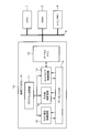
- FIG. 1 is a diagram schematically illustrating the configuration of the distance detection device according to the first embodiment.
- FIG. 2 is a diagram schematically illustrating a specific configuration of the processing unit.
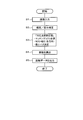
- FIG. 3 is a flowchart schematically showing the contents of the distance calculation process.
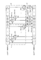
- FIG. 4 is a diagram schematically showing the configuration of the cost correction processing circuit.
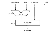
- FIG. 5 is a diagram schematically illustrating the configuration of the ACS circuit in the dividing unit.
- FIG. 6 is a diagram schematically illustrating the configuration of the ACS circuit in the integration unit.
- FIG. 7 is a diagram schematically illustrating a first configuration example of the cost correction processing circuit according to the second embodiment.
- FIG. 8 is a diagram schematically illustrating a second configuration example of the cost correction processing circuit according to the second embodiment.
- a distance detection device 1 shown in FIG. 1 is a device that detects a distance to each point in a captured image by detecting parallax of a plurality of captured images.
- the distance detection device 1 is designed so that the correspondence between pixels constituting a plurality of captured images, that is, parallax can be obtained with high accuracy by applying the Viterbi algorithm, which is a dynamic programming method, in a plurality of directions. ing.
- the distance detection device 1 is mounted on a vehicle such as a passenger car, and includes two imaging units 2 and 3, a processing unit 4, and a vehicle control unit 5.
- the imaging units 2 and 3 are not limited to two, and for example, three or more imaging units may be provided.
- the imaging units 2 and 3 are each configured as a known camera in which the traveling direction of the vehicle is within the imaging range.
- the imaging units 2 and 3 constitute a stereo camera, and are set so as to perform simultaneous and periodic imaging.
- the processing unit 4 acquires captured images captured by the imaging units 2 and 3 and executes various processes described later.
- the vehicle control unit 5 executes processing for controlling the vehicle using the processing result obtained by the processing unit 4. For example, the vehicle control unit 5 acquires distance information at each point in the imaging range by the imaging units 2 and 3 from the processing unit 4, and recognizes the target position and the relative speed based on the distance information. And the vehicle control part 5 performs vehicle control, such as changing a driving
- the function of the processing unit 4 can be realized by, for example, a configuration as shown in FIG. That is, in this case, the processing unit 4 includes a CPU 7, a DMA controller 8, a main memory 9, and a dedicated accelerator 10 that are communicably connected via the bus 6.
- the dedicated accelerator 10 includes a program control unit 11, a cost correction processing circuit 12, other arithmetic circuits 13, a load / store control circuit 14, a local memory 15, and a data register 16.
- the basic operation and functions of the above configuration are as follows. That is, the host CPU 7 notifies the dedicated accelerator 10 of a target processing request. Data to be processed is sequentially transferred from the main memory 9 to the local memory 15 of the dedicated accelerator 10 via the DMA controller 8.
- the program control unit 11 reads a target processing program based on a processing request from the CPU 7, and transmits a control signal for specifying a target process, a target register, and the like to each circuit.
- the load / store control circuit 14 loads or stores an array in units of a plurality of data from the local memory 15 based on the control signal.
- the cost correction processing circuit 12 and the other arithmetic circuit 13 read and process the data of the target register based on the control signal, and write it back to the register.
- the program control unit 11 transfers a completion notification to the CPU 7 and the DMA controller 8. Further, the completed processing data is transferred from the local memory 15 to the main memory 9 via the DMA controller 8. Thereafter, the host CPU 7 determines the next processing and transfers the next processing request to the dedicated accelerator 10.
- the processing unit 4 executes various processes by repeating the above operation.
- the processing unit 4 performs the same processing as the distance calculation processing disclosed in Japanese Patent Laid-Open No. 2015-114269 (hereinafter also referred to as Literature 1). That is, as shown in FIG. 3, first, in step S1, captured images captured by the imaging units 2 and 3 are acquired. In the subsequent step S2, processing such as correction of image distortion or posture deviation by the lens of the captured image is performed, and the captured image is collimated.
- step S3 corresponding point search processing is performed.
- the correspondence between each pixel constituting a reference image that is a captured image by the imaging unit 2 and each pixel that constitutes a comparison image that is a captured image by the imaging unit 3, for example, the same thing is captured.
- the process of associating locations Since the specific content of the corresponding point search processing is disclosed in Document 1, description thereof is omitted here.
- step S4 the distance to the target shown in each pixel is calculated according to the parallax of the corresponding point in each pixel.
- step S ⁇ b> 5 correspondence data between these pixels and distances is output to the vehicle control unit 5.
- the circuit that performs the sequential processing is divided into a plurality of blocks and operated in parallel, and each of the blocks that are operated in parallel The results were compared and integrated.
- the cost correction processing circuit 12 of the present embodiment has a configuration as shown in FIG. Note that the cost correction processing circuit 12 corresponds to an arithmetic device that executes arithmetic processing using the previous arithmetic result for each of a plurality of input data in a predetermined order.
- the cost correction processing circuit 12 divides a circuit for performing sequential processing into a first-half division unit 21 and a second-half division unit 22 and performs parallel processing, and finally integrates the results of each stage by the integration unit 23.
- each data of the input data array input to the cost correction processing circuit 12 is referred to as input data [1], input data [2],..., Input data [N], and the cost correction processing circuit 12
- the data of the output data array output from is called output data [1], output data [2],..., Output data [N].
- the number N of these data is an even number.
- the first division unit 21 includes ACS circuits 24 [2] to 24 [N / 2] that use the input data [2] to [N / 2] as input data, respectively.
- the latter half division unit 22 includes ACS circuits 24 [N / 2 + 2] to 24 [N] that use the input data [N / 2 + 2] to [N] as input data, respectively.
- the ACS circuit 24 [2] to the ACS circuit 24 [N] may be collectively referred to as the ACS circuit 24.
- the ACS circuit 24 has a configuration as shown in FIG. That is, the ACS circuit 24 includes an adder 25 and a comparison selector 26.
- the adder 25 adds a constant ⁇ to the calculation result output from the previous stage.
- the constant ⁇ is a positive value
- the adder 25 performs pure addition.
- the value of the constant ⁇ can be changed as appropriate by register setting or the like.
- the comparison selector 26 compares the output data of the adder 25 with the input data at the main stage, selects a value satisfying a predetermined condition from the data, and outputs the selected value as a calculation result at the main stage. Specifically, the comparison selector 26 selects the smaller value of each data and outputs it as the operation result of this stage.
- the ACS circuit 24 [2] adds the constant ⁇ to the input data [1] and compares it with the input data [2], and outputs the smaller value as the operation result of the main stage and the ACS of the next stage. Output to the circuit 24 [3] as the previous calculation result. Then, the ACS circuit 24 [3] in the next stage adds a constant ⁇ to the operation result in the previous stage output from the ACS circuit 24 [2] and compares it with the input data [3]. While outputting as the calculation result of this stage, it outputs as the calculation result of the previous stage to the ACS circuit 24 [4] of the next stage.
- the ACS circuit 24 [N / 2 + 2] adds a constant ⁇ to the input data [N / 2 + 1] and compares it with the input data [N / 2 + 2], and uses the smaller value as the operation result of this stage. And output to the next stage ACS circuit 24 [N / 2 + 3] as the calculation result of the previous stage. Then, the next stage ACS circuit 24 [N / 2 + 3] adds the constant ⁇ to the previous stage calculation result output from the ACS circuit 24 [N / 2 + 2] and compares it with the input data [N / 2 + 3]. The smaller value is output to the integration unit 23 as the calculation result of the main stage and is output as the calculation result of the previous stage to the ACS circuit 24 [N / 2 + 4] of the next stage.
- the input data [1] becomes the output data [1] as it is, and the calculation results output from the ACS circuits 24 [2] to 24 [N / 2] included in the first division unit 21 are output. Data [2] to [N / 2]. However, the calculation result output from the ACS circuit 24 [N / 2] is also given to the integration unit 23.
- the integrating unit 23 includes ACS circuits 27 [N / 2 + 1] to 27 [N] that use the output of each stage of the dividing unit 22 as input data.
- the ACS circuit 27 [N / 2 + 1] to the ACS circuit 27 [N] may be collectively referred to as the ACS circuit 27.
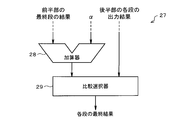
- the ACS circuit 27 has a configuration as shown in FIG. In other words, the ACS circuit 27 includes an adder 28 and a comparison selector 29.
- the adder 28 adds ⁇ to the result of the last stage of the first half, that is, the calculation result output from the ACS circuit 24 [N / 2].
- ⁇ is a value obtained by multiplying a number representing the order in the latter half by a constant ⁇ .
- the comparison selector 29 compares the output data of the adder 28 and the calculation result output from each stage of the dividing unit 22 and outputs the smaller value as the final result of each stage in the latter half.
- the final result is output as output data [N / 2 + 1].
- the cost correction processing circuit 12 executes the ACS operation using the previous operation result for each of the input data [1] to [N] in the input data array according to the order of the input data array. Then, the cost correction processing circuit 12 divides a series of ACS calculation processes for the plurality of input data [1] to [N] into the first half and the second half in the above order, and executes the division units 21 and 22 that execute each in parallel. And an integration unit 23 that collectively compares and integrates the calculation results output from the final stage of the first-half division unit 21 for each calculation result output from each stage of the second-half division unit 22. .
- the cost correction processing circuit 12 divides a series of ACS calculation processes for a plurality of input data [1] to [N] into two parts, the first half and the second half, but this division number is three. That's all.
- two configuration examples obtained by dividing a series of ACS calculation processes into four will be described with reference to FIGS. 7 and 8.
- a series of ACS calculation processes are divided into four division units 31 to 34 in the order of the input data array and are processed in parallel. Integrate the results.
- the dividing unit 31 includes ACS circuits 24 [2] to 24 [N / 4] that use the input data [2] to [N / 4] as input data, respectively.
- the dividing unit 32 includes ACS circuits 24 [N / 4 + 2] to 24 [N / 2] that use the input data [N / 4 + 2] to [N / 2] as input data, respectively.
- the dividing unit 33 includes ACS circuits 24 [N / 2 + 2] to 24 [3N / 4] that use the input data [N / 2 + 2] to [3N / 4] as input data, respectively.
- the dividing unit 34 includes ACS circuits 24 [3N / 4 + 2] to 24 [N] that use the input data [3N / 4 + 2] to [N] as input data, respectively.
- the input data [1] becomes the output data [1] as it is, and the calculation results output from the ACS circuits 24 [2] to 24 [N / 4] included in the dividing unit 31 are output data [1]. 2] to [N / 4].
- the calculation result output from the ACS circuit 24 [N / 4] is also given to the integration unit 35.
- the integration unit 35 includes a first integration block 35a, a second integration block 35b, and a third integration block 35c.
- the first integrated block 35a includes ACS circuits 27 [N / 4 + 1] to 27 [N / 2] using the output of each stage of the dividing unit 32 as input data.
- the adders 28 of the ACS circuits 27 [N / 4 + 1] to 27 [N / 2] add ⁇ to the result of the final stage of the dividing unit 31, that is, the calculation result output from the ACS circuit 24 [N / 4]. It is like that. Therefore, the first integrated block 35a compares the data proportional to the calculation result of the final stage of the dividing unit 31 and the calculation result output from each stage of the dividing unit 32, and calculates the smaller value. Select and output as output data [N / 4 + 1] to [N / 2].
- the second integrated block 35b includes ACS circuits 27 [N / 2 + 1] to 27 [3N / 4] that use the output of each stage of the dividing unit 33 as input data.
- the adders 28 of the ACS circuits 27 [N / 2 + 1] to 27 [3N / 4] add ⁇ to the result of the final stage of the first integrated block 35a, that is, the calculation result output from the ACS circuit 27 [N / 2]. It comes to add. Therefore, the second integrated block 35b is proportional to the output data [N / 2] that is the calculation result after being output from the final stage of the dividing unit 32 and being integrated via the first integrated block 35a. The data is compared with the calculation result output from each stage of the dividing unit 33, and the smaller value is selected and output as output data [N / 2 + 1] to [3N / 4].
- the third integrated block 35c includes ACS circuits 27 [3N / 4 + 1] to 27 [N] that use the output of each stage of the dividing unit 34 as input data.
- the adders 28 of the ACS circuits 27 [3N / 4 + 1] to 27 [N] add ⁇ to the result of the final stage of the second integrated block 35b, that is, the calculation result output from the ACS circuit 27 [3N / 4]. It is like that. Therefore, the third integrated block 35c is in a proportional relationship with the output data [3N / 4] that is the calculation result output from the final stage of the dividing unit 33 and integrated through the second integrated block 35b. The data is compared with the calculation result output from each stage of the dividing unit 34, and the smaller value is selected and output as output data [3N / 4 + 1] to [N].
- the integration unit 35 of the first configuration example performs the integration process by combining the first and second division units 31 and 32 in order, and each stage of the division units 33 and 34 in the third and subsequent orders. For each of the calculation results output from, the calculation results output from the division unit one order earlier than them and integrated after the integration processing are collectively compared and output as the final result It has become.
- the integration unit 35 has three stages in the order of “(1) integration by the first integration block 35a ⁇ (2) integration by the second integration block 35b ⁇ (3) integration by the third integration block 35c”. Integration processing will be performed.
- the integration unit 41 includes a first integration block 41a, a second integration block 41b, and a third integration block 41c.
- the first integrated block 41a has the same configuration as the first integrated block 35a of the first configuration example. Therefore, the first integrated block 41a compares the data proportional to the calculation result of the final stage of the dividing unit 31 and the calculation result output from each stage of the dividing unit 32, and calculates the smaller value. Select and output as output data [N / 4 + 1] to [N / 2].
- the second integrated block 41b includes ACS circuits 27 [3N / 4 + 1] to 27 [N] that use the output of each stage of the dividing unit 34 as input data.
- the adders 28 of the ACS circuits 27 [3N / 4 + 1] to 27 [N] add ⁇ to the result of the final stage of the dividing unit 33, that is, the calculation result output from the ACS circuit 24 [3N / 4]. It has become. Therefore, the second integrated block 41b compares the data proportional to the calculation result of the final stage of the dividing unit 33 and the calculation result output from each stage of the dividing unit 34, and calculates the smaller value. Select and output.
- the third integrated block 41c receives the output of each stage of the ACS circuit 27 [N / 2 + 1] to 27 [3N / 4] using the output of each stage of the dividing unit 33 as input data and the output of each stage of the second integrated block 41b.
- ACS circuits 42 [3N / 4 + 1] to 42 [N] serving as input data are provided.
- the ACS circuits 42 [3N / 4 + 1] to 42 [N] have the same configuration as the ACS circuit 27.
- the ACS circuits 42 [3N / 4 + 1] to 42 [N] may be collectively referred to as the ACS circuit 42.
- the adders 28 of the ACS circuits 27 [N / 2 + 1] to 27 [3N / 4] and the ACS circuits 42 [3N / 4 + 1] to 42 [N] are the result of the final stage of the first integrated block 41a, that is, the ACS circuit 27. ⁇ is added to the calculation result output from [N / 2]. Therefore, the third integrated block 41c is proportional to the output data [N / 2], which is the calculation result after being output from the final stage of the dividing unit 32 and integrated via the first integrated block 41a. The data is compared with the calculation result output from each stage of the dividing unit 33, and the smaller value is selected and output as output data [N / 2 + 1] to [3N / 4].
- the third integrated block 41c calculates data after being output from each stage of the dividing unit 34 and being integrated via the second integrated block 41b, with data proportional to the output data [N / 2]. The result is compared, and the smaller value is selected and output as output data [3N / 4 + 1] to [N].
- the integration unit 41 of the second configuration example performs integration processing by combining two division units 31 and 32 that are adjacent in order, and also sets two division units 33 and 34 that are adjacent in order. Perform integration processing.
- the integration unit 41 further performs integration processing on the two sets that have been subjected to integration processing, and outputs the result as a final result.
- the integration unit 41 performs integration processing in two stages in the order of “(1) integration by the first integration block 41a and integration by the second integration block 41b ⁇ (2) integration by the third integration block 41c”. Will be done.
- the integration unit 35 of the first configuration example can reduce the number of ACS circuits as compared with the integration unit 41 of the second configuration example, and thus the circuit scale can be reduced.
- the integration unit 41 of the second configuration example can suppress the number of stages passing through the ACS circuit to be smaller than that of the integration unit 35 of the first configuration example, so that the time required for the arithmetic processing can be further shortened. Therefore, when the number of divisions in a series of ACS calculation processes is set to 4 or more, an optimum configuration may be used so as to satisfy specifications such as a circuit scale and a processing time in consideration of such points.
- the ACS operation is “addition ⁇ minimum comparison”, but may be “subtraction ⁇ maximum comparison”. That is, in each of the above embodiments, the constant ⁇ is a positive value, but it may be a negative value. Then, the adders 25 and 28 substantially perform subtraction. In this case, the comparison selectors 26 and 29 may select the larger one of the two input values and output it as a calculation result. That is, in this case, the larger value is “a value that satisfies a predetermined condition”.
- each division unit when dividing a series of ACS calculation processing, each division unit is equally divided, but it is not always necessary to equally divide.
- the number of data N in the input data array is an even number, but the number of data N may be an odd number.
- a series of ACS calculation processes are divided into a plurality along the order of the input data array.
- the present invention is not limited to this, and may be divided into a plurality according to a predetermined order.
- the ACS circuits of the integration units 23, 35, and 41 it is possible to omit the subsequent stage portion. For example, if the data on the adder side is determined not to be the minimum value in the comparison and selection in the predetermined ACS circuit in the integration unit and is temporarily rejected, the data on the adder side is always used in the comparison and selection in the subsequent ACS circuit. Is rejected.
- the ACS circuit is omitted thereafter, and It is also possible not to perform a process of collectively comparing the calculation results. In this way, it is possible to reduce the circuit scale. Even in such a case, the accuracy of the calculation is not greatly reduced.
Landscapes
- Engineering & Computer Science (AREA)
- Theoretical Computer Science (AREA)
- Physics & Mathematics (AREA)
- Software Systems (AREA)
- General Physics & Mathematics (AREA)
- General Engineering & Computer Science (AREA)
- Data Mining & Analysis (AREA)
- Mathematical Physics (AREA)
- Mathematical Optimization (AREA)
- Pure & Applied Mathematics (AREA)
- Databases & Information Systems (AREA)
- Mathematical Analysis (AREA)
- Computational Mathematics (AREA)
- Algebra (AREA)
- Image Processing (AREA)
- Advance Control (AREA)
- Complex Calculations (AREA)
- Image Analysis (AREA)
Abstract
演算装置(12)は、複数の入力データのそれぞれに対し、前段の演算結果を用いる演算処理を所定の順序に従い実行する。前記演算処理は、前記複数の入力データのうちいずれか1つの入力データと、前段の演算結果に所定の定数を加算したデータとを比較し、それら各データのうち予め定めた条件を満たす値を選択して演算結果として出力する加算比較選択演算である。前記演算装置は、前記複数の入力データに対する一連の前記演算処理を前記順序に沿って複数に分割し、それぞれを並列に実行する分割部(21、22、31~34)と、前記順序が隣り合う2つの分割部のうち前記順序が後の分割部の各段から出力される演算結果のそれぞれに対し前記順序が前の分割部の最終段から出力される演算結果を一括比較して統合する統合処理を実行する統合部(23、35、41)と、を備える。
Description
本出願は、2016年4月12日に出願された日本出願番号2016-079586号に基づくもので、ここにその記載内容を援用する。
本開示は、加算比較選択演算を繰り返し実行する演算装置に関する。
近年、自動車の事故防止や自動運転化のために、車載カメラによる測距や認識処理のニーズが高まっている。車載向けの画像処理装置は組み込みシステムのため、限られた性能およびリソースで要求時間内での処理を実現する必要がある。例えば、ステレオカメラは原理的に模様の少ない物体の測距が難しい。そのため、グローバル法という視差画像全体の滑らかさを考慮する手法を導入することにより、弱パタンである路面などもロバストに検出することができる手法が近年開発されている。このような方法の主なものとして、Viterbi(以下、ビタビと呼ぶ)アルゴリズムと呼ばれる動的計画法の一種により、全体のコストが最小になる視差の組み合わせを決定するものがある。
ビタビアルゴリズムの計算量としては、その遷移状態、つまりノードの数が増えると、指数関数的に処理量が増える。そして、ステレオカメラの場合、遷移状態数が視差の数(通常、数十~数百以上の数)だけあるため、計算量が大きくなる。このような課題に対して、アルゴリズムに着目し、既に計算した隣の遷移状態の結果を再利用することにより、従来ではノード数の2乗に比例していた計算量を、ノード数の2倍程度の計算量に抑えることを実現する手法が考えられている(例えば、特許文献1参照)。このような手法によれば、処理時間の短縮が可能になるが、ステレオカメラの数百万画素にわたって上記処理を車載のような組み込み環境で実現するためには、更なる高速化が必要となる。
ビタビ演算の高速化の課題に対し、ビタビ演算の基本処理要素である加算・比較・選択(以下、ACSと呼ぶ)回路を直列に接続した専用回路が提案されている(例えば、特許文献2参照)。この手法によれば、単一のACS回路を再帰的に用いる場合に比べ、クロックの受け渡しでの処理時間のオーバーヘッドを減らせる分だけ高速化が期待できる。しかし、この場合、通過するACS回路の段数は少なくなっておらず、スループットの向上には限界がある。
本開示の目的は、演算の精度を良好に維持しつつ、演算の高速化を実現することができる演算装置を提供することにある。
本開示の第一の態様において、演算装置は、複数の入力データのそれぞれに対し、前段の演算結果を用いる演算処理を所定の順序に従い実行する。その演算処理は、複数の入力データのうちいずれか1つの入力データと、前段の演算結果に所定の定数を加算したデータとを比較し、それら各データのうち予め定めた条件を満たす値を選択して演算結果として出力する加算比較選択演算である。上記演算装置は、複数の入力データに対する一連の演算処理を上記順序に沿って複数に分割し、それぞれを並列に実行する分割部と、上記順序が隣り合う2つの分割部のうち順序が後の分割部の各段から出力される演算結果のそれぞれに対し順序が前の分割部の最終段から出力される演算結果を一括比較して統合する統合部と、を備える。
本開示の第一の態様において、演算装置は、複数の入力データのそれぞれに対し、前段の演算結果を用いる演算処理を所定の順序に従い実行する。その演算処理は、複数の入力データのうちいずれか1つの入力データと、前段の演算結果に所定の定数を加算したデータとを比較し、それら各データのうち予め定めた条件を満たす値を選択して演算結果として出力する加算比較選択演算である。上記演算装置は、複数の入力データに対する一連の演算処理を上記順序に沿って複数に分割し、それぞれを並列に実行する分割部と、上記順序が隣り合う2つの分割部のうち順序が後の分割部の各段から出力される演算結果のそれぞれに対し順序が前の分割部の最終段から出力される演算結果を一括比較して統合する統合部と、を備える。
このような構成によれば、一連の演算処理を複数に分割して並列に実行するので、一連の演算処理を逐次的に処理する場合に比べ、演算処理に要する時間が短縮される。また、統合部を設けたことにより、順序が後の分割部から出力される演算結果についても、順序が前の分割部における演算結果を考慮したものとなり、演算が不正確になることはない。したがって、上記構成によれば、演算の精度を良好に維持しつつ、演算の高速化を実現することができる。
本開示についての上記目的およびその他の目的、特徴や利点は、添付の図面を参照しながら下記の詳細な記述により、より明確になる。その図面は、
図1は、第1実施形態に係る距離検出装置の構成を模式的に示す図であり、
図2は、処理部の具体的な構成を模式的に示す図であり、
図3は、距離演算処理の内容を模式的に示すフローチャートであり、
図4は、コスト補正処理回路の構成を模式的に示す図であり、
図5は、分割部におけるACS回路の構成を模式的に示す図であり、
図6は、統合部におけるACS回路の構成を模式的に示す図であり、
図7は、第2実施形態に係るコスト補正処理回路の第1構成例を模式的に示す図であり、
図8は、第2実施形態に係るコスト補正処理回路の第2構成例を模式的に示す図である。
以下、複数の実施形態について図面を参照して説明する。なお、各実施形態において実質的に同一の構成には同一の符号を付して説明を省略する。
(第1実施形態)
以下、第1実施形態について図1~図6を参照して説明する。
(第1実施形態)
以下、第1実施形態について図1~図6を参照して説明する。
図1に示す距離検出装置1は、複数の撮像画像の視差を検出することによって撮像画像中の各点までの距離を検出する装置である。距離検出装置1では、動的計画法であるビタビアルゴリズムを複数の方向に適用することで複数の撮像画像を構成する画素間の対応関係、つまり視差を高精度に求めることができるように配慮されている。
距離検出装置1は、乗用車などの車両に搭載されており、2つの撮像部2、3、処理部4および車両制御部5を備えている。なお、撮像部2、3は、2つに限らずともよく、例えば3つ以上設けられていてもよい。撮像部2、3は、それぞれ車両の進行方向が撮像範囲内となる周知のカメラとして構成されている。撮像部2、3は、ステレオカメラを構成しており、周期的に同時に撮像を行うように設定されている。
処理部4は、撮像部2、3により撮像された撮像画像を取得し、後述する各種処理を実行する。車両制御部5は、処理部4による処理結果を用いて車両を制御する処理を実行する。例えば、車両制御部5は、撮像部2、3による撮像範囲内の各点における距離の情報を処理部4から取得し、その距離の情報に基づいて物標位置および相対速度を認識する。そして、車両制御部5は、物標が走行に支障をきたすおそれがある場合、走行軌道を変更するなどの車両制御を実行する。
処理部4の機能は、例えば、図2に示すような構成により実現することができる。すなわち、この場合、処理部4は、バス6を介して通信可能に接続されたCPU7、DMAコントローラ8、メインメモリ9および専用アクセラレータ10により構成される。専用アクセラレータ10は、プログラム制御部11、コスト補正処理回路12、その他演算回路13、ロードストア制御回路14、ローカルメモリ15およびデータレジスタ16を備えている。
上記構成の基本的な動作および機能は、次の通りである。すなわち、ホストCPU7は、専用アクセラレータ10に対し、対象とする処理依頼を通知する。また、メインメモリ9から処理対象のデータがDMAコントローラ8を介して専用アクセラレータ10のローカルメモリ15に順次転送される。
プログラム制御部11は、CPU7からの処理依頼に基づいて対象の処理プログラムを読み出し、各回路に対して対象処理や対象レジスタなどを指定する制御信号を送信する。ロードストア制御回路14は、上記制御信号に基づいてローカルメモリ15から複数データを単位とした配列をデータレジスタにロードまたはストアする。
コスト補正処理回路12およびその他演算回路13は、上記制御信号に基づいて対象レジスタのデータを読み出して処理を行い、レジスタに書き戻す。プログラム制御部11は、処理プログラムが完了すると、CPU7およびDMAコントローラ8に完了通知を転送する。また、ローカルメモリ15から完了した処理データがDMAコントローラ8を介してメインメモリ9に転送される。その後、ホストCPU7は、次の処理を判断し、次の処理依頼を専用アクセラレータ10に転送する。処理部4は、以上のような動作を繰り返すことにより、各種の処理を実行する。
本実施形態の距離検出装置1において、処理部4は、特開2015-114269号公報(以下、文献1とも呼ぶ)に開示された距離演算処理と同様の処理を行う。すなわち、図3に示すように、まず、ステップS1では、撮像部2、3により撮像された撮像画像が取得される。続くステップS2では、撮像画像のレンズによる画像の歪や姿勢のずれを補正するなどの処理が行われ、撮像された画像が平行化される。
ステップS3では、対応点探索処理が実施される。対応点探索処理は、例えば撮像部2による撮像画像である基準画像を構成する各画素と、例えば撮像部3による撮像画像である比較画像を構成する各画素との対応関係、つまり同じものが写っている場所を関連付ける処理である。対応点探索処理の具体的な内容は、文献1に開示されているため、ここでの説明は省略する。続いて、ステップS4では、各画素における対応点の視差に応じて各画素に写っている物標までの距離が算出される。そして、ステップS5では、これらの画素と距離との対応データが車両制御部5に対して出力される。
ただし、本実施形態では、対応点探索処理に対し、以下に説明するような工夫を加えることで、演算の更なる高速化を実現している。すなわち、文献1の対応点探索処理では、1つ前までの最小コスト結果を再利用することで総当たり計算を二項比較の反復に直し、処理負荷の削減が図られている。そして、本願の発明者は、このような文献1では「s(u,v)=u-v」としているが、「s(u,v)=λ│u-v│」であれば線形性が保たれることを見出した。ただし、λは所定の定数である。この場合、前の結果にλを加算して次のノードの値と比較し、小さいほうの値を次の結果とする、といったことが繰り返される。つまり、この場合、ACS演算が基本の繰り返し単位となる。
ここで、ACS演算を行うACS回路を直列に接続する従来技術を用いると、1つ前の結果を用いる演算および選択が直列に反復処理される、つまり逐次的に処理されるため、多段接続による回路遅延などに起因する速度低下の影響が大きい。そこで、このような逐次処理を分割して並列に実行することが考えられる。しかし、演算結果がその後の演算に依存するような逐次処理を、単純に分割して並列化すると、計算が不正確になり、精度が低下するといった懸念がある。
これらの点を考慮し、本実施形態では、遷移コストの線形性を導入することを前提として、逐次処理を行う回路を複数のブロックに分割して並列動作させ、それら並列動作させた各ブロックにおける結果を一括比較して統合するようにした。具体的には、本実施形態のコスト補正処理回路12は、図4に示すような構成を有している。なお、コスト補正処理回路12は、複数の入力データのそれぞれに対し、前段の演算結果を用いる演算処理を所定の順序に従い実行する演算装置に相当する。
コスト補正処理回路12は、逐次処理を行う回路を前半の分割部21と後半の分割部22とに分割して並列処理し、最後に統合部23により各段の結果を統合する。なお、以下では、コスト補正処理回路12に入力される入力データ配列の各データのことを入力データ[1],入力データ[2],…,入力データ[N]と呼び、コスト補正処理回路12から出力される出力データ配列の各データのことを出力データ[1],出力データ[2],…,出力データ[N]と呼ぶこととする。また、本実施形態では、これらのデータ数Nは、偶数となっている。
前半の分割部21は、入力データ[2]~[N/2]をそれぞれ入力データとするACS回路24[2]~24[N/2]を備えている。また、後半の分割部22は、入力データ[N/2+2]~[N]をそれぞれ入力データとするACS回路24[N/2+2]~24[N]を備えている。なお、以下では、ACS回路24[2]~ACS回路24[N]のことをACS回路24と総称することがある。
ACS回路24は、図5に示すような構成となっている。すなわち、ACS回路24は、加算器25および比較選択器26を備えている。加算器25は、前段から出力される演算結果に定数λを加算する。なお、本実施形態では、定数λは正の値となっており、加算器25は純粋に加算を行うものである。また、定数λの値は、レジスタ設定などにより適宜変更することが可能となっている。比較選択器26は、加算器25の出力データと本段の入力データとを比較し、それら各データのうち予め定めた条件を満たす値を選択して本段の演算結果として出力する。具体的には、比較選択器26は、各データのうちいずれか小さいほうの値を選択して本段の演算結果として出力する。
例えば、ACS回路24[2]は、入力データ[1]に定数λを加算して入力データ[2]と比較し、小さいほうの値を本段の演算結果として出力するとともに、次段のACS回路24[3]に対し前段の演算結果として出力する。そして、次段のACS回路24[3]は、ACS回路24[2]から出力された前段の演算結果に定数λを加算して入力データ[3]と比較し、いずれか小さいほうの値を本段の演算結果として出力するとともに、次段のACS回路24[4]に対し前段の演算結果として出力する。
また、ACS回路24[N/2+2]は、入力データ[N/2+1]に定数λを加算して入力データ[N/2+2]と比較し、小さいほうの値を本段の演算結果として統合部23に出力するとともに、次段のACS回路24[N/2+3]に対し前段の演算結果として出力する。そして、次段のACS回路24[N/2+3]は、ACS回路24[N/2+2]から出力された前段の演算結果に定数λを加算して入力データ[N/2+3]と比較し、いずれか小さいほうの値を本段の演算結果として統合部23に出力するとともに、次段のACS回路24[N/2+4]に対し前段の演算結果として出力する。
このような構成において、入力データ[1]がそのまま出力データ[1]となり、前半の分割部21が備えるACS回路24[2]~24[N/2]から出力される演算結果が、それぞれ出力データ[2]~[N/2]となる。ただし、ACS回路24[N/2]から出力される演算結果は、統合部23にも与えられる。
統合部23は、分割部22の各段の出力をそれぞれ入力データとするACS回路27[N/2+1]~27[N]を備えている。なお、以下では、ACS回路27[N/2+1]~ACS回路27[N]のことをACS回路27と総称することがある。
ACS回路27は、図6に示すような構成となっている。すなわち、ACS回路27は、加算器28および比較選択器29を備えている。加算器28は、前半の最終段の結果、つまりACS回路24[N/2]から出力される演算結果にαを加算する。αは、後半における順番を表す数に定数λを乗じた値である。
例えば、ACS回路27[N/2+1]の場合、後半における順番が「1」であるため「α=1×λ」となり、ACS回路27[N/2+2]の場合、後半における順番が「2」であるため「α=2×λ」となり、ACS回路27[N]の場合、後半における順番が「N/2」であるため「α=(N/2)×λ」となる。したがって、ACS回路27[X]とすると、αは下記(1)で表される。
α=(X-N/2)×λ …(1)
α=(X-N/2)×λ …(1)
比較選択器29は、加算器28の出力データと分割部22の各段から出力される演算結果とを比較し、いずれか小さいほうの値を後半の各段の最終結果として出力する。例えば、ACS回路27[N/2+1]は、前半の最終段の演算結果にα(=1×λ)を加算して入力データ[N/2+1]と比較し、小さいほうの値を本段の最終結果、つまり出力データ[N/2+1]として出力する。また、ACS回路27[N/2+2]は、前半の最終段の演算結果にα(=2×λ)を加算してACS回路24[N/2+2]から出力される演算結果と比較し、小さいほうの値を本段の最終結果、つまり出力データ[N/2+2]として出力する。
このようなACS回路27を有する統合部23は、分割部21の最終段の演算結果と比例関係にあるデータ(=加算器28の出力データ)と、分割部22の各段から出力される演算結果とを比較し、いずれか小さいほうの値を一連のACS演算処理における後半の各段の最終結果として出力するようになっている。つまり、統合部23は、後半の分割部22の各段から出力される演算結果のそれぞれに対し前半の分割部21の最終段から出力される演算結果を一括比較して統合するようになっている。
以上説明した本実施形態によれば、次のような効果が得られる。
本実施形態のコスト補正処理回路12は、入力データ配列の各入力データ[1]~[N]のそれぞれに対し、前段の演算結果を用いるACS演算を入力データ配列の順序に従い実行する。そして、コスト補正処理回路12は、複数の入力データ[1]~[N]に対する一連のACS演算処理を上記順序に沿って前半と後半に分割し、それぞれを並列に実行する分割部21、22と、後半の分割部22の各段から出力される演算結果のそれぞれに対し前半の分割部21の最終段から出力される演算結果を一括比較して統合する統合部23と、を備えている。
本実施形態のコスト補正処理回路12は、入力データ配列の各入力データ[1]~[N]のそれぞれに対し、前段の演算結果を用いるACS演算を入力データ配列の順序に従い実行する。そして、コスト補正処理回路12は、複数の入力データ[1]~[N]に対する一連のACS演算処理を上記順序に沿って前半と後半に分割し、それぞれを並列に実行する分割部21、22と、後半の分割部22の各段から出力される演算結果のそれぞれに対し前半の分割部21の最終段から出力される演算結果を一括比較して統合する統合部23と、を備えている。
このような構成によれば、一連のACS演算処理を2つに分割して並列に実行するので、一連のACS演算処理を逐次的に処理する場合に比べ、回路遅延の短縮などを期待することができ、その結果、演算処理に要する時間が約半分程度に短縮される。しかも一連のACS演算処理を単純に並列化しただけでなく、統合部23を設けているため、後半の分割部22から出力される演算結果についても、前半の分割部21での演算結果を考慮したものとなり、演算が不正確になるおそれはない。したがって、本実施形態によれば、演算の精度を良好に維持しつつ、演算の高速化を実現することができる。このような演算の高速化、つまり処理時間の削減による効果は、車載のような組み込み環境において、一層有益なものとなる。
(第2実施形態)
第1実施形態では、コスト補正処理回路12は、複数の入力データ[1]~[N]に対する一連のACS演算処理を前半と後半の2つに分割していたが、この分割数は3つ以上でもよい。本実施形態では、一連のACS演算処理を4つに分割した2つの構成例について図7および図8を参照して説明する。
第1実施形態では、コスト補正処理回路12は、複数の入力データ[1]~[N]に対する一連のACS演算処理を前半と後半の2つに分割していたが、この分割数は3つ以上でもよい。本実施形態では、一連のACS演算処理を4つに分割した2つの構成例について図7および図8を参照して説明する。
<第1構成例>
図7に示すように、第1構成例では、一連のACS演算処理を入力データ配列の順序に沿って4つの分割部31~34に分割して並列処理し、最後に統合部35により各段の結果を統合する。分割部31は、入力データ[2]~[N/4]をそれぞれ入力データとするACS回路24[2]~24[N/4]を備えている。分割部32は、入力データ[N/4+2]~[N/2]をそれぞれ入力データとするACS回路24[N/4+2]~24[N/2]を備えている。
図7に示すように、第1構成例では、一連のACS演算処理を入力データ配列の順序に沿って4つの分割部31~34に分割して並列処理し、最後に統合部35により各段の結果を統合する。分割部31は、入力データ[2]~[N/4]をそれぞれ入力データとするACS回路24[2]~24[N/4]を備えている。分割部32は、入力データ[N/4+2]~[N/2]をそれぞれ入力データとするACS回路24[N/4+2]~24[N/2]を備えている。
分割部33は、入力データ[N/2+2]~[3N/4]をそれぞれ入力データとするACS回路24[N/2+2]~24[3N/4]を備えている。分割部34は、入力データ[3N/4+2]~[N]をそれぞれ入力データとするACS回路24[3N/4+2]~24[N]を備えている。
このような構成において、入力データ[1]がそのまま出力データ[1]となり、分割部31が備えるACS回路24[2]~24[N/4]から出力される演算結果が、それぞれ出力データ[2]~[N/4]となる。ただし、ACS回路24[N/4]から出力される演算結果は、統合部35にも与えられる。
統合部35は、第1統合ブロック35a、第2統合ブロック35bおよび第3統合ブロック35cを備えている。第1統合ブロック35aは、分割部32の各段の出力をそれぞれ入力データとするACS回路27[N/4+1]~27[N/2]を備えている。ACS回路27[N/4+1]~27[N/2]の加算器28は、分割部31の最終段の結果、つまりACS回路24[N/4]から出力される演算結果にαを加算するようになっている。したがって、第1統合ブロック35aは、分割部31の最終段の演算結果と比例関係にあるデータと、分割部32の各段から出力される演算結果とを比較し、いずれか小さいほうの値を選択して出力データ[N/4+1]~[N/2]として出力する。
第2統合ブロック35bは、分割部33の各段の出力をそれぞれ入力データとするACS回路27[N/2+1]~27[3N/4]を備えている。ACS回路27[N/2+1]~27[3N/4]の加算器28は、第1統合ブロック35aの最終段の結果、つまりACS回路27[N/2]から出力される演算結果にαを加算するようになっている。したがって、第2統合ブロック35bは、分割部32の最終段から出力されて第1統合ブロック35aを介して統合が行われた後の演算結果である出力データ[N/2]と比例関係にあるデータと、分割部33の各段から出力される演算結果とを比較し、いずれか小さいほうの値を選択して出力データ[N/2+1]~[3N/4]として出力する。
第3統合ブロック35cは、分割部34の各段の出力をそれぞれ入力データとするACS回路27[3N/4+1]~27[N]を備えている。ACS回路27[3N/4+1]~27[N]の加算器28は、第2統合ブロック35bの最終段の結果、つまりACS回路27[3N/4]から出力される演算結果にαを加算するようになっている。したがって、第3統合ブロック35cは、分割部33の最終段から出力されて第2統合ブロック35bを介して統合が行われた後の演算結果である出力データ[3N/4]と比例関係にあるデータと、分割部34の各段から出力される演算結果とを比較し、いずれか小さいほうの値を選択して出力データ[3N/4+1]~[N]として出力する。
このように、第1構成例の統合部35は、順序が1番目、2番目の分割部31、32を組にして統合処理を行い、順序が3番目以降の分割部33、34の各段から出力される演算結果のそれぞれに対し、それらより順序が1つ前の分割部から出力されて統合処理が行われた後の演算結果を一括比較して統合し、最終結果として出力するようになっている。なお、この場合、統合部35では、「(1)第1統合ブロック35aによる統合→(2)第2統合ブロック35bによる統合→(3)第3統合ブロック35cによる統合」という順に、3段階で統合処理が行われることになる。
<第2構成例>
図8に示すように、第2構成例では、第1構成例と同様に、一連のACS演算処理を入力データ配列の順序に沿って4つの分割部31~34に分割して並列処理し、最後に統合部41により各段の結果を統合する。統合部41は、第1統合ブロック41a、第2統合ブロック41bおよび第3統合ブロック41cを備えている。
図8に示すように、第2構成例では、第1構成例と同様に、一連のACS演算処理を入力データ配列の順序に沿って4つの分割部31~34に分割して並列処理し、最後に統合部41により各段の結果を統合する。統合部41は、第1統合ブロック41a、第2統合ブロック41bおよび第3統合ブロック41cを備えている。
第1統合ブロック41aは、第1構成例の第1統合ブロック35aと同様の構成となっている。したがって、第1統合ブロック41aは、分割部31の最終段の演算結果と比例関係にあるデータと、分割部32の各段から出力される演算結果とを比較し、いずれか小さいほうの値を選択して出力データ[N/4+1]~[N/2]として出力する。
第2統合ブロック41bは、分割部34の各段の出力をそれぞれ入力データとするACS回路27[3N/4+1]~27[N]を備えている。ACS回路27[3N/4+1]~27[N]の加算器28は、分割部33の最終段の結果、つまりACS回路24[3N/4]から出力される演算結果にαを加算するようになっている。したがって、第2統合ブロック41bは、分割部33の最終段の演算結果と比例関係にあるデータと、分割部34の各段から出力される演算結果とを比較し、いずれか小さいほうの値を選択して出力する。
第3統合ブロック41cは、分割部33の各段の出力をそれぞれ入力データとするACS回路27[N/2+1]~27[3N/4]と、第2統合ブロック41bの各段の出力をそれぞれ入力データとするACS回路42[3N/4+1]~42[N]と、を備えている。なお、ACS回路42[3N/4+1]~42[N]は、ACS回路27と同様の構成である。また、以下では、ACS回路42[3N/4+1]~42[N]のことをACS回路42と総称することがある。
ACS回路27[N/2+1]~27[3N/4]およびACS回路42[3N/4+1]~42[N]の加算器28は、第1統合ブロック41aの最終段の結果、つまりACS回路27[N/2]から出力される演算結果にαを加算するようになっている。したがって、第3統合ブロック41cは、分割部32の最終段から出力されて第1統合ブロック41aを介して統合が行われた後の演算結果である出力データ[N/2]と比例関係にあるデータと、分割部33の各段から出力される演算結果とを比較し、いずれか小さいほうの値を選択して出力データ[N/2+1]~[3N/4]として出力する。また、第3統合ブロック41cは、出力データ[N/2]と比例関係にあるデータと、分割部34の各段から出力されて第2統合ブロック41bを介して統合が行われた後の演算結果とを比較し、いずれか小さいほうの値を選択して出力データ[3N/4+1]~[N]として出力する。
このように、第2構成例の統合部41は、順序が隣り合う2つの分割部31、32を組にして統合処理を行うとともに、順序が隣り合う2つの分割部33、34を組にして統合処理を行う。そして、統合部41は、統合処理が行われた2つの組に対してさらに統合処理を行い、最終結果として出力するようになっている。なお、この場合、統合部41では、「(1)第1統合ブロック41aによる統合および第2統合ブロック41bによる統合→(2)第3統合ブロック41cによる統合」という順に、2段階で統合処理が行われることになる。
以上説明した本実施形態によっても、第1実施形態と同様に、演算の精度を良好に維持しつつ、演算の高速化を実現することができる。なお、第1構成例および第2構成例は、それぞれにメリットがある。すなわち、第1構成例の統合部35は、第2構成例の統合部41に比べ、ACS回路の数を少なくできるため、その回路規模を小さくすることができる。また、第2構成例の統合部41は、第1構成例の統合部35に比べ、ACS回路を通過する段数を小さく抑えることができるため、演算処理に要する時間を更に短縮することができる。したがって、一連のACS演算処理の分割数を4以上にする場合、このような点を考慮したうえで、回路規模や処理時間などの仕様を満たすように、最適な構成を用いればよい。
(その他の実施形態)
なお、本開示は上記し且つ図面に記載した各実施形態に限定されるものではなく、その要旨を逸脱しない範囲で任意に変形、組み合わせ、あるいは拡張することができる。
なお、本開示は上記し且つ図面に記載した各実施形態に限定されるものではなく、その要旨を逸脱しない範囲で任意に変形、組み合わせ、あるいは拡張することができる。
上記各実施形態では、ACS演算は「加算→最小比較」であったが、「減算→最大比較」としてもよい。すなわち、上記各実施形態では定数λを正の値としていたが、これを負の値としてもよい。そうすると、加算器25、28は、実質的に減算を行うものとなる。この場合、比較選択器26、29は、2つの入力値のうち、いずれか大きいほうの値を選択して演算結果として出力すればよい。つまり、この場合、いずれか大きい値が「予め定めた条件を満たす値」となる。
上記各実施形態では、一連のACS演算処理を分割する際、それぞれの分割部を等分するようにしていたが、必ずしも等分する必要はない。また、上記各実施形態では、入力データ配列のデータ数Nは偶数としていたが、データ数Nは奇数でもよい。
上記各実施形態では一連のACS演算処理を、入力データ配列の順序に沿って複数に分割していたが、これに限らずともよく、所定の順序に沿って複数に分割すればよい。
統合部23、35、41のACS回路のうち、後段部分を省略することも可能である。例えば、統合部における所定のACS回路での比較選択において加算器側のデータが最小値ではないとされて一旦棄却された場合、その後段のACS回路での比較選択においても必ず加算器側のデータは棄却される。そこで、予め実験やシミュレーションなどで、統合部の後半のある所で非常に高い確率で加算器側のデータが棄却されることが判明していれば、それ以降はACS回路を省略し、前段の演算結果を一括比較して統合する処理を行わないことも可能である。このようにすれば、回路規模を小さくできるという効果が得られる。なお、このようにした場合でも、大きく演算の精度が低下することはない。
統合部23、35、41のACS回路のうち、後段部分を省略することも可能である。例えば、統合部における所定のACS回路での比較選択において加算器側のデータが最小値ではないとされて一旦棄却された場合、その後段のACS回路での比較選択においても必ず加算器側のデータは棄却される。そこで、予め実験やシミュレーションなどで、統合部の後半のある所で非常に高い確率で加算器側のデータが棄却されることが判明していれば、それ以降はACS回路を省略し、前段の演算結果を一括比較して統合する処理を行わないことも可能である。このようにすれば、回路規模を小さくできるという効果が得られる。なお、このようにした場合でも、大きく演算の精度が低下することはない。
本開示は、実施例に準拠して記述されたが、本開示は当該実施例や構造に限定されるものではないと理解される。本開示は、様々な変形例や均等範囲内の変形をも包含する。加えて、様々な組み合わせや形態、さらには、それらに一要素のみ、それ以上、あるいはそれ以下、を含む他の組み合わせや形態をも、本開示の範疇や思想範囲に入るものである。
Claims (4)
- 複数の入力データのそれぞれに対し、前段の演算結果を用いる演算処理を所定の順序に従い実行する演算装置(12)であって、
前記演算処理は、前記複数の入力データのうちいずれか1つの入力データと、前段の演算結果に所定の定数を加算したデータとを比較し、それら各データのうち予め定めた条件を満たす値を選択して演算結果として出力する加算比較選択演算であり、
前記複数の入力データに対する一連の前記演算処理を、前記順序に沿って複数に分割し、それぞれを並列に実行する分割部(21、22、31~34)と、
前記順序が隣り合う2つの分割部のうち前記順序が後の分割部の各段から出力される演算結果のそれぞれに対し前記順序が前の分割部の最終段から出力される演算結果を一括比較して統合する統合処理を実行する統合部(23、35、41)と、
を備える演算装置。 - 前記分割部(21、22)は、前記複数の入力データに対する一連の前記演算処理を、前記順序の前半および後半の2つに分割し、それぞれを並列に実行するものであり、
前記統合部(23)は、後半の前記分割部の各段から出力される演算結果のそれぞれに対し、前半の前記分割部の最終段から出力される演算結果を一括比較して統合する請求項1に記載の演算装置。 - 前記分割部(31~34)は、前記複数の入力データに対する一連の前記演算処理を、前記順序に沿って3つ以上に分割し、それぞれを並列に実行するものであり、
前記統合部(35)は、前記順序が3番目以降の分割部の各段から出力される演算結果のそれぞれに対し、当該分割部より前記順序が1つ前の分割部から出力されて前記統合が行われた後の演算結果を一括比較して統合する請求項1に記載の演算装置。 - 前記分割部(31~34)は、前記複数の入力データに対する一連の前記演算処理を、前記順序に沿って3つ以上に分割し、それぞれを並列に実行するものであり、
前記統合部(41)は、前記順序が隣り合う2つの分割部を組に対して前記統合処理を実行し、前記統合処理が実行された組のうち順序が隣り合う2つの組に対してさらに前記統合処理を実行する請求項1に記載の演算装置。
Applications Claiming Priority (2)
| Application Number | Priority Date | Filing Date | Title |
|---|---|---|---|
| JP2016-079586 | 2016-04-12 | ||
| JP2016079586A JP6583111B2 (ja) | 2016-04-12 | 2016-04-12 | 演算装置 |
Publications (1)
| Publication Number | Publication Date |
|---|---|
| WO2017179260A1 true WO2017179260A1 (ja) | 2017-10-19 |
Family
ID=60042510
Family Applications (1)
| Application Number | Title | Priority Date | Filing Date |
|---|---|---|---|
| PCT/JP2017/002127 Ceased WO2017179260A1 (ja) | 2016-04-12 | 2017-01-23 | 演算装置 |
Country Status (2)
| Country | Link |
|---|---|
| JP (1) | JP6583111B2 (ja) |
| WO (1) | WO2017179260A1 (ja) |
Citations (1)
| Publication number | Priority date | Publication date | Assignee | Title |
|---|---|---|---|---|
| JP2003085566A (ja) * | 2001-09-10 | 2003-03-20 | Nippon Hoso Kyokai <Nhk> | 対応点探索方法及びこれを用いたマッチング装置 |
-
2016
- 2016-04-12 JP JP2016079586A patent/JP6583111B2/ja not_active Expired - Fee Related
-
2017
- 2017-01-23 WO PCT/JP2017/002127 patent/WO2017179260A1/ja not_active Ceased
Patent Citations (1)
| Publication number | Priority date | Publication date | Assignee | Title |
|---|---|---|---|---|
| JP2003085566A (ja) * | 2001-09-10 | 2003-03-20 | Nippon Hoso Kyokai <Nhk> | 対応点探索方法及びこれを用いたマッチング装置 |
Also Published As
| Publication number | Publication date |
|---|---|
| JP2017191405A (ja) | 2017-10-19 |
| JP6583111B2 (ja) | 2019-10-02 |
Similar Documents
| Publication | Publication Date | Title |
|---|---|---|
| US10474908B2 (en) | Unified deep convolutional neural net for free-space estimation, object detection and object pose estimation | |
| CN107688855B (zh) | 针对于复杂神经网络的分层量化方法与装置 | |
| US20190095212A1 (en) | Neural network system and operating method of neural network system | |
| KR20180012439A (ko) | 회선 신경망에서 가속기 및 이의 동작 방법 | |
| CN113168558B (zh) | 用于图像数据的语义分割的方法、人工神经网络、设备、计算机程序和机器可读存储介质 | |
| US20110249869A1 (en) | System and method for efficient image feature extraction | |
| US11195083B2 (en) | Object detection system and object detection method | |
| CN110816541B (zh) | 弯道识别方法、装置、计算机设备和存储介质 | |
| KR20110049643A (ko) | 한정된 개수의 계층상에 레이블 전파를 위한 정렬 격자 | |
| US20230101250A1 (en) | Method for generating a graph structure for training a graph neural network | |
| US10026148B2 (en) | Image recognition method, image recognition device and image recognition program | |
| US10229472B2 (en) | Image processing apparatus, image processing method, and vehicle control apparatus | |
| KR101766149B1 (ko) | 저연산 스테레오 영상 매칭 장치 및 방법 | |
| US20180089555A1 (en) | Neural network device and method of operating neural network device | |
| JP6583111B2 (ja) | 演算装置 | |
| US11822326B2 (en) | Voter-based method of controlling redundancy, electronic device, and storage medium | |
| CN116724315A (zh) | 确定神经网络的编码器架构的方法 | |
| CN113447031B (zh) | 坡度点筛选方法、终端设备及介质和坡度计算方法及系统 | |
| US20220309351A1 (en) | Structure transformation device, structure transformation method, and computer readable medium | |
| JP7239747B2 (ja) | 情報処理装置 | |
| CN110097183B (zh) | 信息处理方法以及信息处理系统 | |
| Ćorić et al. | Implementation of different image edge detection algorithms on a real embedded ADAS platform | |
| KR20230077845A (ko) | 사물 검출기 경량화를 위한 균형 잡힌 지식 증류 방법 및 장치 | |
| US20240256901A1 (en) | Information processing apparatus, information processing method and non-transitory computer-readable storage medium | |
| US20190073584A1 (en) | Apparatus and methods for forward propagation in neural networks supporting discrete data |
Legal Events
| Date | Code | Title | Description |
|---|---|---|---|
| NENP | Non-entry into the national phase |
Ref country code: DE |
|
| 121 | Ep: the epo has been informed by wipo that ep was designated in this application |
Ref document number: 17782079 Country of ref document: EP Kind code of ref document: A1 |
|
| 122 | Ep: pct application non-entry in european phase |
Ref document number: 17782079 Country of ref document: EP Kind code of ref document: A1 |