WO2017170046A1 - Focusing mechanism and imaging module - Google Patents
Focusing mechanism and imaging module Download PDFInfo
- Publication number
- WO2017170046A1 WO2017170046A1 PCT/JP2017/011477 JP2017011477W WO2017170046A1 WO 2017170046 A1 WO2017170046 A1 WO 2017170046A1 JP 2017011477 W JP2017011477 W JP 2017011477W WO 2017170046 A1 WO2017170046 A1 WO 2017170046A1
- Authority
- WO
- WIPO (PCT)
- Prior art keywords
- optical lens
- focusing mechanism
- lens
- piezoelectric actuator
- optical
- Prior art date
Links
- 238000003384 imaging method Methods 0.000 title claims abstract description 16
- 230000003287 optical effect Effects 0.000 claims abstract description 128
- 239000010408 film Substances 0.000 claims description 36
- 239000000463 material Substances 0.000 claims description 32
- 230000003068 static effect Effects 0.000 claims description 14
- 229910021420 polycrystalline silicon Inorganic materials 0.000 claims description 10
- 229920005591 polysilicon Polymers 0.000 claims description 10
- 239000010409 thin film Substances 0.000 claims description 10
- 150000004767 nitrides Chemical class 0.000 claims description 2
- 238000006073 displacement reaction Methods 0.000 abstract description 22
- 238000000034 method Methods 0.000 description 21
- XUIMIQQOPSSXEZ-UHFFFAOYSA-N Silicon Chemical compound [Si] XUIMIQQOPSSXEZ-UHFFFAOYSA-N 0.000 description 16
- 229910052710 silicon Inorganic materials 0.000 description 16
- 239000010703 silicon Substances 0.000 description 16
- 239000000758 substrate Substances 0.000 description 16
- 238000004519 manufacturing process Methods 0.000 description 12
- 229910052581 Si3N4 Inorganic materials 0.000 description 9
- HQVNEWCFYHHQES-UHFFFAOYSA-N silicon nitride Chemical compound N12[Si]34N5[Si]62N3[Si]51N64 HQVNEWCFYHHQES-UHFFFAOYSA-N 0.000 description 9
- 239000011347 resin Substances 0.000 description 8
- 229920005989 resin Polymers 0.000 description 8
- 239000000853 adhesive Substances 0.000 description 6
- 230000001070 adhesive effect Effects 0.000 description 6
- 238000005530 etching Methods 0.000 description 5
- 238000010791 quenching Methods 0.000 description 5
- 238000004544 sputter deposition Methods 0.000 description 4
- 239000004809 Teflon Substances 0.000 description 3
- 229920006362 Teflon® Polymers 0.000 description 3
- 238000005229 chemical vapour deposition Methods 0.000 description 3
- 230000000593 degrading effect Effects 0.000 description 3
- 238000001312 dry etching Methods 0.000 description 3
- 238000001459 lithography Methods 0.000 description 3
- 239000002184 metal Substances 0.000 description 3
- 239000000203 mixture Substances 0.000 description 3
- HBMJWWWQQXIZIP-UHFFFAOYSA-N silicon carbide Chemical compound [Si+]#[C-] HBMJWWWQQXIZIP-UHFFFAOYSA-N 0.000 description 3
- OKTJSMMVPCPJKN-UHFFFAOYSA-N Carbon Chemical compound [C] OKTJSMMVPCPJKN-UHFFFAOYSA-N 0.000 description 2
- 239000004593 Epoxy Substances 0.000 description 2
- KRHYYFGTRYWZRS-UHFFFAOYSA-N Fluorane Chemical compound F KRHYYFGTRYWZRS-UHFFFAOYSA-N 0.000 description 2
- YCKRFDGAMUMZLT-UHFFFAOYSA-N Fluorine atom Chemical compound [F] YCKRFDGAMUMZLT-UHFFFAOYSA-N 0.000 description 2
- VYPSYNLAJGMNEJ-UHFFFAOYSA-N Silicium dioxide Chemical compound O=[Si]=O VYPSYNLAJGMNEJ-UHFFFAOYSA-N 0.000 description 2
- 229910052782 aluminium Inorganic materials 0.000 description 2
- PNEYBMLMFCGWSK-UHFFFAOYSA-N aluminium oxide Inorganic materials [O-2].[O-2].[O-2].[Al+3].[Al+3] PNEYBMLMFCGWSK-UHFFFAOYSA-N 0.000 description 2
- 229910021417 amorphous silicon Inorganic materials 0.000 description 2
- 229910052802 copper Inorganic materials 0.000 description 2
- 229910021419 crystalline silicon Inorganic materials 0.000 description 2
- UHESRSKEBRADOO-UHFFFAOYSA-N ethyl carbamate;prop-2-enoic acid Chemical compound OC(=O)C=C.CCOC(N)=O UHESRSKEBRADOO-UHFFFAOYSA-N 0.000 description 2
- 239000011737 fluorine Substances 0.000 description 2
- 229910052731 fluorine Inorganic materials 0.000 description 2
- 239000011521 glass Substances 0.000 description 2
- 229910052737 gold Inorganic materials 0.000 description 2
- 230000005484 gravity Effects 0.000 description 2
- 229910000040 hydrogen fluoride Inorganic materials 0.000 description 2
- AMGQUBHHOARCQH-UHFFFAOYSA-N indium;oxotin Chemical compound [In].[Sn]=O AMGQUBHHOARCQH-UHFFFAOYSA-N 0.000 description 2
- 229910052451 lead zirconate titanate Inorganic materials 0.000 description 2
- 238000005259 measurement Methods 0.000 description 2
- 238000000691 measurement method Methods 0.000 description 2
- 229910052751 metal Inorganic materials 0.000 description 2
- 229910044991 metal oxide Inorganic materials 0.000 description 2
- 150000004706 metal oxides Chemical class 0.000 description 2
- 229910052759 nickel Inorganic materials 0.000 description 2
- 229910052758 niobium Inorganic materials 0.000 description 2
- 229910052594 sapphire Inorganic materials 0.000 description 2
- 239000010980 sapphire Substances 0.000 description 2
- 229910010271 silicon carbide Inorganic materials 0.000 description 2
- 229910052814 silicon oxide Inorganic materials 0.000 description 2
- 229910002076 stabilized zirconia Inorganic materials 0.000 description 2
- 229910001220 stainless steel Inorganic materials 0.000 description 2
- 239000010935 stainless steel Substances 0.000 description 2
- 229910052718 tin Inorganic materials 0.000 description 2
- 238000001947 vapour-phase growth Methods 0.000 description 2
- 239000004925 Acrylic resin Substances 0.000 description 1
- 241000877463 Lanio Species 0.000 description 1
- 239000004698 Polyethylene Substances 0.000 description 1
- 239000004793 Polystyrene Substances 0.000 description 1
- 229910004121 SrRuO Inorganic materials 0.000 description 1
- ATJFFYVFTNAWJD-UHFFFAOYSA-N Tin Chemical compound [Sn] ATJFFYVFTNAWJD-UHFFFAOYSA-N 0.000 description 1
- 230000004075 alteration Effects 0.000 description 1
- 238000000137 annealing Methods 0.000 description 1
- 229910052787 antimony Inorganic materials 0.000 description 1
- 229910052793 cadmium Inorganic materials 0.000 description 1
- 229910052799 carbon Inorganic materials 0.000 description 1
- 229910052804 chromium Inorganic materials 0.000 description 1
- 230000001010 compromised effect Effects 0.000 description 1
- 238000000151 deposition Methods 0.000 description 1
- 230000008021 deposition Effects 0.000 description 1
- 238000007599 discharging Methods 0.000 description 1
- 230000000694 effects Effects 0.000 description 1
- 238000005516 engineering process Methods 0.000 description 1
- 238000011156 evaluation Methods 0.000 description 1
- 238000010304 firing Methods 0.000 description 1
- 239000002783 friction material Substances 0.000 description 1
- 229910052733 gallium Inorganic materials 0.000 description 1
- 229910002804 graphite Inorganic materials 0.000 description 1
- 239000010439 graphite Substances 0.000 description 1
- 229910052735 hafnium Inorganic materials 0.000 description 1
- 229910052738 indium Inorganic materials 0.000 description 1
- 238000001746 injection moulding Methods 0.000 description 1
- 229910052741 iridium Inorganic materials 0.000 description 1
- 229910052742 iron Inorganic materials 0.000 description 1
- HFGPZNIAWCZYJU-UHFFFAOYSA-N lead zirconate titanate Chemical compound [O-2].[O-2].[O-2].[O-2].[O-2].[Ti+4].[Zr+4].[Pb+2] HFGPZNIAWCZYJU-UHFFFAOYSA-N 0.000 description 1
- 239000011344 liquid material Substances 0.000 description 1
- 229910052749 magnesium Inorganic materials 0.000 description 1
- 229910052748 manganese Inorganic materials 0.000 description 1
- 238000002488 metal-organic chemical vapour deposition Methods 0.000 description 1
- 229910052750 molybdenum Inorganic materials 0.000 description 1
- CWQXQMHSOZUFJS-UHFFFAOYSA-N molybdenum disulfide Chemical compound S=[Mo]=S CWQXQMHSOZUFJS-UHFFFAOYSA-N 0.000 description 1
- 229910052982 molybdenum disulfide Inorganic materials 0.000 description 1
- 238000000059 patterning Methods 0.000 description 1
- 238000005268 plasma chemical vapour deposition Methods 0.000 description 1
- 229910052697 platinum Inorganic materials 0.000 description 1
- -1 polyethylene Polymers 0.000 description 1
- 229920000573 polyethylene Polymers 0.000 description 1
- 229920000642 polymer Polymers 0.000 description 1
- 229920002223 polystyrene Polymers 0.000 description 1
- 230000002265 prevention Effects 0.000 description 1
- 230000001681 protective effect Effects 0.000 description 1
- 229910052706 scandium Inorganic materials 0.000 description 1
- 239000007921 spray Substances 0.000 description 1
- 229910052715 tantalum Inorganic materials 0.000 description 1
- 229910052719 titanium Inorganic materials 0.000 description 1
- 229910052721 tungsten Inorganic materials 0.000 description 1
- 238000009281 ultraviolet germicidal irradiation Methods 0.000 description 1
- 229910052720 vanadium Inorganic materials 0.000 description 1
- 238000001039 wet etching Methods 0.000 description 1
- 229910052727 yttrium Inorganic materials 0.000 description 1
- VWQVUPCCIRVNHF-UHFFFAOYSA-N yttrium atom Chemical compound [Y] VWQVUPCCIRVNHF-UHFFFAOYSA-N 0.000 description 1
- 229910052725 zinc Inorganic materials 0.000 description 1
Images


Classifications
-
- G—PHYSICS
- G02—OPTICS
- G02B—OPTICAL ELEMENTS, SYSTEMS OR APPARATUS
- G02B7/00—Mountings, adjusting means, or light-tight connections, for optical elements
- G02B7/02—Mountings, adjusting means, or light-tight connections, for optical elements for lenses
- G02B7/04—Mountings, adjusting means, or light-tight connections, for optical elements for lenses with mechanism for focusing or varying magnification
- G02B7/08—Mountings, adjusting means, or light-tight connections, for optical elements for lenses with mechanism for focusing or varying magnification adapted to co-operate with a remote control mechanism
-
- G—PHYSICS
- G02—OPTICS
- G02B—OPTICAL ELEMENTS, SYSTEMS OR APPARATUS
- G02B7/00—Mountings, adjusting means, or light-tight connections, for optical elements
- G02B7/02—Mountings, adjusting means, or light-tight connections, for optical elements for lenses
- G02B7/04—Mountings, adjusting means, or light-tight connections, for optical elements for lenses with mechanism for focusing or varying magnification
- G02B7/10—Mountings, adjusting means, or light-tight connections, for optical elements for lenses with mechanism for focusing or varying magnification by relative axial movement of several lenses, e.g. of varifocal objective lens
-
- G—PHYSICS
- G02—OPTICS
- G02B—OPTICAL ELEMENTS, SYSTEMS OR APPARATUS
- G02B7/00—Mountings, adjusting means, or light-tight connections, for optical elements
- G02B7/02—Mountings, adjusting means, or light-tight connections, for optical elements for lenses
-
- G—PHYSICS
- G02—OPTICS
- G02B—OPTICAL ELEMENTS, SYSTEMS OR APPARATUS
- G02B7/00—Mountings, adjusting means, or light-tight connections, for optical elements
- G02B7/02—Mountings, adjusting means, or light-tight connections, for optical elements for lenses
- G02B7/023—Mountings, adjusting means, or light-tight connections, for optical elements for lenses permitting adjustment
-
- G—PHYSICS
- G02—OPTICS
- G02B—OPTICAL ELEMENTS, SYSTEMS OR APPARATUS
- G02B7/00—Mountings, adjusting means, or light-tight connections, for optical elements
- G02B7/02—Mountings, adjusting means, or light-tight connections, for optical elements for lenses
- G02B7/026—Mountings, adjusting means, or light-tight connections, for optical elements for lenses using retaining rings or springs
-
- G—PHYSICS
- G02—OPTICS
- G02B—OPTICAL ELEMENTS, SYSTEMS OR APPARATUS
- G02B7/00—Mountings, adjusting means, or light-tight connections, for optical elements
- G02B7/02—Mountings, adjusting means, or light-tight connections, for optical elements for lenses
- G02B7/04—Mountings, adjusting means, or light-tight connections, for optical elements for lenses with mechanism for focusing or varying magnification
-
- H—ELECTRICITY
- H02—GENERATION; CONVERSION OR DISTRIBUTION OF ELECTRIC POWER
- H02N—ELECTRIC MACHINES NOT OTHERWISE PROVIDED FOR
- H02N2/00—Electric machines in general using piezoelectric effect, electrostriction or magnetostriction
- H02N2/0005—Electric machines in general using piezoelectric effect, electrostriction or magnetostriction producing non-specific motion; Details common to machines covered by H02N2/02 - H02N2/16
- H02N2/0075—Electrical details, e.g. drive or control circuits or methods
-
- H—ELECTRICITY
- H10—SEMICONDUCTOR DEVICES; ELECTRIC SOLID-STATE DEVICES NOT OTHERWISE PROVIDED FOR
- H10N—ELECTRIC SOLID-STATE DEVICES NOT OTHERWISE PROVIDED FOR
- H10N30/00—Piezoelectric or electrostrictive devices
- H10N30/20—Piezoelectric or electrostrictive devices with electrical input and mechanical output, e.g. functioning as actuators or vibrators
- H10N30/204—Piezoelectric or electrostrictive devices with electrical input and mechanical output, e.g. functioning as actuators or vibrators using bending displacement, e.g. unimorph, bimorph or multimorph cantilever or membrane benders
- H10N30/2041—Beam type
- H10N30/2042—Cantilevers, i.e. having one fixed end
Definitions
- the present invention relates to a focusing mechanism including a piezoelectric element and an optical lens, and an imaging module.
- VCM Voice Coil Motor
- Patent Document 1 discloses a method using an electrostatic actuator as a minute drive mechanism that moves an optical lens.
- the drive mechanism described in Patent Document 1 is complicated because it produces a sufficient amount of displacement with a very small size, and the production yield and drive durability are problems.
- Patent Document 2 discloses a method of using a flexible material such as a polymer as a lens material and changing the focal length by deforming the lens, not a method of focusing by moving the optical lens. .
- a flexible material such as a polymer
- the aberration of the lens is deteriorated and the optical characteristics are inferior, so the image quality of the photographed photograph must be compromised.
- Patent Documents 3 and 4 disclose a method of deforming a lens by using a liquid material for the drive system and the lens itself.
- the mechanism is complicated, and the image quality of photographic images is expected to be inferior to that of a fixed optical lens.
- Patent Document 5 discloses an optical module that drives an optical lens with a piezoelectric film formed directly along the outer periphery of the optical lens.
- a piezoelectric film is directly formed on the outer periphery of the optical element, and the piezoelectric film has a structure that is strongly constrained, so that it is difficult to output a high amount of displacement.
- the present invention has been made in view of the above circumstances, and provides a focusing mechanism capable of moving an optical lens with a high displacement with a simple structure and capable of being driven at high speed and with low power consumption. Objective. It is another object of the present invention to provide an imaging module that can be driven at high speed and with low power consumption with a simple structure without degrading the quality of image quality.
- the focusing mechanism of the present invention is A drive source in which three or more cantilever piezoelectric actuators are arranged radially; An outer frame, an optical lens, a lens holding unit that holds the optical lens around the optical lens, and an optical lens unit that includes an elastic body that connects the lens holding unit to the outer frame and expands and contracts in the radial direction of the optical lens; With The cantilever type piezoelectric actuator is in contact with the lens holding portion at a surface perpendicular to the optical axis direction of the optical lens at the driving tip of the cantilever type piezoelectric actuator, and the optical lens is moved in the optical axis direction of the optical lens by driving the cantilever type piezoelectric actuator. Move and focus.
- the surface perpendicular to the driving direction of the cantilever piezoelectric actuator is preferably covered with a material having a static friction coefficient of 0.5 or less.
- a protrusion is provided on a surface perpendicular to the drive direction of the cantilever piezoelectric actuator, and the protrusion is in contact with the lens holding portion.
- the surface of the protrusion may be covered with a material having a static friction coefficient of 0.5 or less.
- Three or more cantilever piezoelectric actuators may be arranged in a spiral shape.
- the cantilever piezoelectric actuator is preferably made of an isotropic material.
- the isotropic material is polysilicon.
- the cantilever piezoelectric actuator is preferably made of a thin film.
- the elastic body is preferably a bellows-like nitride film.
- the imaging module of the present invention includes the focusing mechanism of the present invention.
- the “driving tip of the cantilever piezoelectric actuator” indicates the tip of the actuator that can obtain the maximum displacement and a certain region from the tip.
- the certain area is determined by the displacement amount of the actuator, the configuration of the lens holding portion, and the like.
- the optical lens can be moved with a high displacement amount with a simple structure, and can be driven at high speed with low power consumption. Further, according to the imaging module of the present invention, it is possible to drive with high speed and low power consumption with a simple structure without degrading the quality of image quality.
- FIG. 1 is a schematic cross-sectional view of an embodiment of a focusing mechanism of the present invention.
- FIG. 2 is a schematic cross-sectional view during driving of an embodiment of the focusing mechanism of the present invention.
- FIG. 3 is a schematic top view of the driving source of the focusing mechanism of the present invention.
- FIG. 4 is a schematic top view of the optical lens unit of the focusing mechanism of the present invention.
- FIG. 5 is a schematic cross-sectional view showing a process of manufacturing a driving source for the focusing mechanism of the present invention.
- FIG. 6 is a schematic cross-sectional view showing a manufacturing process of the optical lens unit of the focusing mechanism of the present invention.
- FIG. 7 is a schematic sectional view showing an imaging module using the focusing mechanism of the present invention.
- FIG. 1 is a schematic cross-sectional view of an embodiment of a focusing mechanism of the present invention.
- FIG. 2 is a schematic cross-sectional view during driving of an embodiment of the focusing mechanism of the
- FIG. 8 is a schematic top view showing a drive source of another embodiment of the focusing mechanism of the present invention.
- FIG. 9 is a schematic top view showing a state in which an optical lens is arranged on a drive source of another embodiment of the focusing mechanism of the present invention.
- FIG. 10 is an enlarged schematic view of the drive source showing the lengths of the actuators arranged in a spiral shape.
- FIG. 11 is a graph showing the voltage of the example and the displacement amount of the optical lens.
- FIG. 1 shows a schematic cross-sectional view of the focusing mechanism of the present invention in a state where no voltage is applied.
- FIG. 2 shows a schematic cross-sectional view of the focusing mechanism of the present invention when a voltage is applied.
- FIG. 3 shows a schematic top view of the drive source.
- FIG. 4 shows a schematic top view of the optical lens unit.
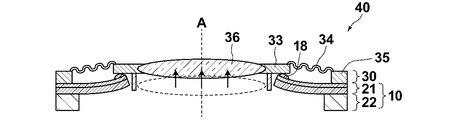
- the focusing mechanism 40 of the present invention includes a drive source 10 in which 32 cantilever piezoelectric actuators 21 (hereinafter simply referred to as actuators) are radially arranged on a ring-shaped support 22.
- actuators cantilever piezoelectric actuators 21
- the actuator 21 is in contact with the lens holding portion 33 at a surface 25 perpendicular to the optical axis direction of the optical lens at the driving tip 24 of the actuator 21, and the optical lens 36 is moved in the optical axis direction A of the optical lens 36 by driving the actuator 21. Move and focus.
- the actuator 21 warps to the upper surface side (upward on the paper surface) due to the unimorph effect. As a result, the optical lens 36 is lifted in the optical axis direction A via the protrusion 18. Since the optical lens 36 is supported by the elastic body 34, the optical lens 36 can move quickly without being constrained.
- the drive source 10 is made up of 32 rectangular actuators 21 arranged radially.
- the actuator 21 is arranged radially with the ring-shaped support body 22 as a common support body.
- the actuator 21 is provided with a protrusion 18 on a surface 25 perpendicular to the optical axis direction A of the optical lens at the driving tip 24.
- the protrusion 18 is in contact with the lens holding portion 33 of the optical lens unit 30. Since the protrusion 18 is provided, the actuator 21 and the lens holding portion 33 are in point contact with each other, so that it is possible to improve the decrease in the displacement due to friction.
- the protrusion 18 is further covered with a material having a static friction coefficient of 0.5 or less (not shown). Since the projection 18 is covered with a material having a static friction coefficient of 0.5 or less, the actuator 21 and the lens holding portion 33 are slippery when driven, and there is almost no structural constraint. In the conventional diaphragm or beam type structure, the displacement is greatly reduced because the actuator is strongly restrained, and the displacement necessary for focusing cannot be achieved. Thus, since the optical lens is supported by a material having a static friction coefficient of 0.5 or less and a low friction, a high displacement can be ideally realized.
- the projection part 18 does not need to be formed.
- the low friction material may be provided on the entire surface 25 or only the driving tip 24.
- the optical lens unit 30 is connected to the outer frame 35, the optical lens 36, the lens holding unit 33 that holds the optical lens 36 around the optical lens 36, and the lens holding unit 33. It consists of an elastic body that expands and contracts in the radial direction of the optical lens 36.
- the elastic body 34 is a bellows structure that is formed all around the optical lens 36 and expands and contracts in the radial direction of the optical lens.
- the optical lens unit 30 is in contact with the protrusion 18 of the drive source 10 on the back surface of the lens holding portion 33 as shown in FIG.
- the optical lens unit 30 is driven by the elastic body 34 so that the optical lens 36 and the lens holding portion 33 do not fall due to gravity or inertia force, or the optical axis of the optical lens 36 does not shift. It is suppressed to the 10 side.
- the elastic body 34 is made of, for example, a silicon nitride film having a bellows structure formed integrally with the lens holding portion 33 and the outer frame 35.
- the bellows structure using the microfabrication technique is used as the elastic body, but it is also possible to use a plurality of springs manufactured using, for example, an injection molding technique. In this case, it does not need to be formed around the entire periphery of the optical lens, and may have a structure in which a plurality of elastic bodies are arranged radially.
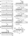
- FIG. 5 shows a schematic cross-sectional view of the manufacturing process of an embodiment of the drive source.
- a silicon substrate 11 is prepared. Since the thickness of the silicon substrate 11 serves as a support for a plurality of cantilever piezoelectric actuators, it is preferably, for example, 300 ⁇ m to 800 ⁇ m from the viewpoint of preventing the entire structure from being deformed by driving the actuator.
- the substrate is not limited to a silicon substrate, and examples of the substrate include glass, stainless steel, yttrium stabilized zirconia (YSZ), alumina, sapphire, and silicon carbide.
- thermal oxide films (silicon oxide) 12 and 13 are formed on the front and back surfaces of the silicon substrate 11.
- the thermal oxide films 12 and 13 serve as etching stoppers.
- the thickness of the thermal oxide film is preferably 0.5 ⁇ m to 3 ⁇ m from the viewpoint of the role of an etching stopper and the manufacturing cost.
- a polysilicon film 14 is formed on the surface of the thermal oxide film 13 on the side where the optical lens unit is disposed by a CVD (Chemical Vapor Deposition) method.
- the film thickness of the polysilicon film 14 is preferably 5 ⁇ m to 30 ⁇ m, for example, from the viewpoint of rigidity and displacement necessary for driving the lens.
- the main material of the actuator 21 is preferably an isotropic material such as polysilicon, amorphous silicon, and amorphous silicon carbide, avoiding crystalline silicon. Since crystalline silicon is an anisotropic material, when an inch lever type piezoelectric actuator having actuators arranged radially is manufactured, the rigidity of the actuator varies in the plane.
- an isotropic material such as polysilicon is preferably used as the main material of the actuator 21.
- the lower electrode 15, the ferroelectric thin film 16, and the upper electrode 17 are sequentially formed on the polysilicon film 14 by sputtering (see FIGS. 5d, 5e, and 5f).
- the ferroelectric thin film 16 is preferably one or more perovskite oxides represented by the following composition formula (1).
- M is composed of V, Nb, Ta, Sb, Cr, Mo, W, Mn, Mg, Sc, Co, Cu, In, Sn, Ga, Zn, Cd, Fe, Ni, Hf, and Al. It contains at least one element selected from the group.
- x, y, and z satisfy the relationships 0 ⁇ y ⁇ b, 0 ⁇ z ⁇ b, and 0 ⁇ b ⁇ yz.
- the perovskite oxide that can be represented by the composition formula (1) may contain Nb as M in the composition formula, and the Nb / (Zr + Ti + M) molar ratio may be 0.10 or more and 0.20 or less. 10 to 0.15 is more preferable.
- sputtering method As a preferable film forming method of the ferroelectric thin film 16, sputtering method, plasma CVD method, MOCVD method (metal organic vapor phase growth method, Metal Organic Chemical Vapor Deposition), firing quench quench method, annealing quench method, and spray quench quench And vapor phase growth methods such as the method.
- MOCVD method metal organic vapor phase growth method, Metal Organic Chemical Vapor Deposition
- firing quench quench method annealing quench method
- spray quench quench And vapor phase growth methods such as the method.
- the sputtering method is particularly preferable.
- the material of the lower electrode 15 and the upper electrode 17 is not particularly limited, Au, Pt, Ir, Ti , IrO 2, RuO 2, LaNiO 3, SrRuO 3, ITO ( indium tin oxide) (Indium Tin Oxide), TiN or the like Metal or metal oxide, and combinations thereof.
- the thickness of the lower electrode 15 and the upper electrode 17 is not particularly limited and is, for example, about 200 nm.
- the film thickness of the ferroelectric thin film 16 is not particularly limited, and is usually 1 ⁇ m or more, for example, 1 ⁇ m to 5 ⁇ m.
- the film thickness of the ferroelectric thin film 16 is preferably 3 ⁇ m or more.
- a protrusion 18 is formed in a region that becomes the driving tip of the actuator.
- the protrusion 18 is in contact with the lens holding portion 33 of the optical lens unit 30.
- the protrusion 18 can be formed, for example, by discharging a UV curable resin material with an inkjet for material deposition, and then curing the dropped droplet by UV irradiation.
- the UV curable resin material include a low-viscosity urethane acrylate resin.
- the surface of the protrusion 18 is preferably covered with a material having a static friction coefficient of 0.5 or less from the viewpoint of preventing a decrease in displacement due to friction with the lens holding portion 33.
- the protrusion itself may be made of a material having a static friction coefficient of 0.5 or less.
- Examples of materials having a static friction coefficient of 0.5 or less include fluorine resins such as Teflon (registered trademark, hereinafter omitted), graphite, molybdenum disulfide, DLC (Diamond-Like Carbon), polyethylene, polystyrene, and the like. Can be mentioned.
- the coefficient of static friction is a value measured by a measurement method based on ISO 8295.
- the resist 19 is protected from the surface of the actuator to the thermal oxide film 13.
- lithography for deep silicon etching is performed from the back surface, the thermal oxide film 12 is removed by wet etching, and the silicon substrate 11 is deep etched by Bosch dry etching.
- the thermal oxide film 13 becomes an etching stop layer (see FIGS. 5k and 5l).
- the thermal oxide film 13 exposed by vapor HF (hydrogen fluoride) etching is removed, and the protective resist 19 is removed by an asher.
- Teflon is sputtered on the surface.
- the thickness of the sputtered film is preferably 40 nm to 500 nm from the viewpoint of wear resistance and prevention of peeling due to residual stress.
- the length of the cantilever piezoelectric actuator means the length in the long side direction from the end of the support to the driving front end surface of the actuator in a region where the actuator 21 is not supported by the support 22. In the present embodiment, as shown in FIG. 5 m, it indicates the distance L 1 from the end portion 26 of the support 22 to the tip surface 23 of the actuator 21.
- each actuator it is preferable to design each actuator as described above.
- the arrangement shape of the cantilevers may be arranged so as to be radial from the center of the circle as in the present embodiment, or may be arranged spirally (in the case of Example 2 described later).
- the driving tips of the plurality of actuators only need to be arranged to form a circle.
- FIG. 6 shows a schematic cross-sectional view of the manufacturing process of the optical lens unit 30.
- a silicon substrate 31 is prepared, and a concavo-convex structure 31a is provided in a region where an elastic body is formed.
- the depth of the concave portion varies depending on the material to be used, but the viewpoint is to maximize the displacement of the actuator 21 and the optical lens is pressed against the driving source 10 so as not to drop due to gravity or inertia.
- the uneven period is preferably 1 ⁇ m to 100 ⁇ m, and preferably about 2 ⁇ m to 20 ⁇ m.
- the substrate glass, stainless steel, yttrium-stabilized zirconia, alumina, sapphire, silicon carbide, or the like can be used in addition to silicon. Further, the thickness of the silicon substrate 31 is preferably about 300 ⁇ m to 800 ⁇ m, for example.
- a silicon nitride film 32 is formed on the surface where the concavo-convex structure 31a is formed.
- This silicon nitride film 32 becomes an elastic body.
- the thickness of the silicon nitride film is preferably 0.1 ⁇ m to 2 ⁇ m and more preferably 0.2 ⁇ m to 1 ⁇ m from the viewpoint of providing strength and elasticity.
- the region 31b where the elastic body 34 is formed and the region 31c where the optical lens 36 is disposed on the back side of the silicon substrate 31 are removed by dry etching in two stages (see FIGS. 6c and 6d).
- the silicon nitride film 32 serves as a stopper.
- a material of the elastic body a film containing at least one material of silicon oxide, Al, Ni, Au, and Cu in addition to silicon nitride can be used.
- the silicon nitride film 32 in the portion 31d where the optical lens is disposed is removed, and the lens holding portion 33, the elastic body 34, and the outer frame 35 are formed.
- the separately prepared optical lens 36 is fixed to the lens holding portion 33 with an adhesive.
- the adhesive it is preferable to use an epoxy die bond resin, a fluorine die bond resin, a silicon die bond resin or the like that does not affect the function of the optical lens.
- the lens holding portion 33 of the optical lens unit 30 is disposed on the projection 18 of the drive source 10 manufactured as described above, and the outer frame 35 of the optical lens unit and the actuator 21 are bonded with an adhesive.
- the adhesive it is preferable to use an epoxy die bond resin.
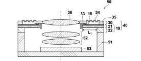
- FIG. 7 is a schematic sectional view showing an embodiment of the imaging module.
- the imaging module 50 according to the present embodiment includes a focusing mechanism 40 according to the present invention that includes a driving source 10 and an optical lens unit 30, and a fixed lens group 52 and an imaging element 53 disposed therein. It is fixed on the casing 51 with an adhesive.
- the optical lens 36 of the optical lens unit 30 moves in the optical axis direction A by the drive of the cantilever piezoelectric actuator 21 and functions as a focusing lens.
- the optical lens 36 serving as a focusing lens and the fixed lens group 52 perform focusing on an object to be imaged at an arbitrary distance to form an optical image on the image sensor 53.
- the imaging module having the focusing mechanism of the present invention uses a cantilever piezoelectric actuator made of a thin film, it is possible to achieve downsizing and low power consumption. Furthermore, since the drive source and the optical lens are not fixed and are in point contact, and the optical lens is supported by an elastic body, the optical lens can quickly move in the optical axis direction. As described above, the imaging module including the focusing mechanism of the present invention can be driven at high speed and with low power consumption without degrading the quality of image quality.
- the driving source of the focusing mechanism has been described in which the actuators are arranged radially.
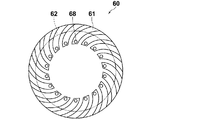
- the driving source may be one in which the actuators are arranged in a spiral shape.
- FIG. 8 shows a schematic top view of the drive source.
- FIG. 9 is a schematic top view showing a state where the optical lens of the drive source is arranged.
- the drive source 60 is formed by arranging 18 actuators 61 having the same shape and the same length on a ring-shaped support body 62 in a spiral shape.
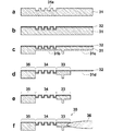
- the actuator 61 has a shape in which the end surface in the major axis direction of the actuator 61 forms an arc.
- a protrusion 68 is provided on a surface perpendicular to the optical axis direction of the optical lens at the driving tip of the actuator 61.
- the optical lens 36 is disposed so that the protrusion 68 is in contact with the lens holding portion 33 of the optical lens unit 30 (see FIG. 9).
- the holding portion, the elastic body, and the outer frame are omitted.
- the lengths of the actuators 61 arranged in a spiral manner as described above are the center L of the tip surface 63 of the actuator 61 and the center of the end where the actuator 61 contacts the support body 62, as shown in FIG. to the the length defined straight line L 2 connecting the between the M.
- a piezoelectric element having a long length can be formed in a narrow region, and without increasing the size of the entire focusing mechanism (or without reducing the size of the optical lens). A high amount of displacement can be obtained.
- Example 1 The driving source and the optical lens unit were manufactured under the following conditions by the manufacturing method described in the embodiment, and the focusing mechanism was manufactured by bonding the driving source and the optical lens unit with an adhesive.
- Silicon substrate diameter 150mm, thickness 350 ⁇ m
- Thermal oxide film 0.5 ⁇ m thickness
- Polysilicon film 10 ⁇ m thick
- Lower electrode Ti (thickness 20 nm) / Ir (thickness 100 nm)
- Upper electrode Ir (thickness 100 nm)
- Piezoelectric film lead zirconate titanate (PZT with 12% Nb added to the B site), thickness 3 ⁇ m
- Cantilever type piezoelectric actuator length L 1 1 mm.
- Protrusion material Low viscosity urethane acrylate UV curable resin
- Protrusion material Teflon (Static friction coefficient 0.1)
- Silicon substrate diameter 150mm, thickness 350 ⁇ m Silicon nitride film: 1 ⁇ m
- Optical lens size Diameter 2.5mm
- Example 2 The focusing mechanism of the second embodiment is the same as that of the first embodiment except that the drive source 60 is used.
- the length L 2 of the cantilevered piezoelectric actuator 61 of the driving source of Example 2 was 2 mm.
- the other drive source configurations are the same as those in the first embodiment.
- Example 1 Lid displacement measurement method- At each applied voltage, the difference in height between the center of the lens 36 and the outer frame 35 was statically measured by a white interference shape measuring device, and the value at a voltage of 0 V was set to zero.
- the measurement results of Example 1 and Example 2 are shown in FIG.
- the focusing mechanism of the present invention obtained a displacement of 50 to 100 ⁇ m at a voltage of 20 to 30V.
- a displacement amount approximately twice as large as that at an applied voltage of 30 V was obtained.
Abstract
[Problem] To provide a focusing mechanism and an imaging module capable of moving an optical lens with a large displacement range using a simple structure, and capable of being driven at high speed with little power consumption.
[Solution] The focusing mechanism comprises: a driving source (10) including three or more radially arranged cantilevered piezoelectric actuator (21); and an optical lens unit (30) including an outer frame (35), an optical lens (36), a lens holder (33) for holding the optical lens (36) along the periphery of the optical lens (36), and an elastic body (34) that connects the lens holder (33) to the outer frame (35) and is flexible along the radial direction of the optical lens (36). The cantilevered piezoelectric actuator (21) is in contact with the lens holder (33) with a surface (25) perpendicular to an optical axis direction A of the optical lens (36) located near a driving tip (24) of the cantilevered piezoelectric actuator (21). The cantilevered piezoelectric actuator (21) is driven which in turn moves the optical lens (36) along the optical axis direction A of the optical lens (36) so as to perform focusing.
Description
本発明は、圧電素子および光学レンズを備えたフォーカシング機構、および撮像モジュールに関する。
The present invention relates to a focusing mechanism including a piezoelectric element and an optical lens, and an imaging module.
近年、携帯電話等に搭載されているカメラには、合焦(フォーカシング)機能が標準で備わっている。その駆動方式のほとんどはボイスコイルモーター(Voice Coil Motor,以下略してVCMと記載する。)である。しかし、VCMは、消費電力が高い、駆動スピードが遅い、さらなる低背化が難しいなどの課題がある。
In recent years, a camera mounted on a mobile phone or the like has a focusing function as a standard feature. Most of the drive systems are voice coil motors (Voice Coil Motor, hereinafter abbreviated as VCM). However, VCM has problems such as high power consumption, low driving speed, and difficulty in further reducing the height.
そこで、VCMに替わる方式として、小型化を実現するため、MEMS(Micro Electro Mechanical Systems)技術などを応用したフォーカシング機構が近年開発されている。例えば、特許文献1には、光学レンズを移動する微小な駆動機構として、静電アクチュエータを使った方法が開示されている。しかし、特許文献1に記載されている駆動機構は、微小なサイズで充分な変位量を出すため複雑になっており、製造歩留まりや駆動耐久性などが課題である。
Therefore, in order to realize miniaturization as a method replacing VCM, a focusing mechanism using MEMS (Micro Electro Mechanical Systems) technology has been developed in recent years. For example, Patent Document 1 discloses a method using an electrostatic actuator as a minute drive mechanism that moves an optical lens. However, the drive mechanism described in Patent Document 1 is complicated because it produces a sufficient amount of displacement with a very small size, and the production yield and drive durability are problems.
また、特許文献2には、光学レンズを移動させて合焦する方法ではなく、レンズ材料にポリマーなどの柔軟なものを使用し、レンズを変形させて焦点距離を変化させる方法が開示されている。しかし、この方法では、レンズの収差が悪化し光学特性が劣るため、撮影写真の画質は妥協せざるを得ない。
Further, Patent Document 2 discloses a method of using a flexible material such as a polymer as a lens material and changing the focal length by deforming the lens, not a method of focusing by moving the optical lens. . However, with this method, the aberration of the lens is deteriorated and the optical characteristics are inferior, so the image quality of the photographed photograph must be compromised.
また、特許文献3および4には、駆動系やレンズ自身に液体材料を用い、レンズを変形させる方法が開示されている。しかし、機構が複雑になり、写真画像の画質も固定の光学レンズの場合と比べると劣ることが予想される。
Patent Documents 3 and 4 disclose a method of deforming a lens by using a liquid material for the drive system and the lens itself. However, the mechanism is complicated, and the image quality of photographic images is expected to be inferior to that of a fixed optical lens.
また、特許文献5には、光学レンズの外周に沿って直接形成された圧電膜で光学レンズを駆動する光学モジュールが開示されている。
Patent Document 5 discloses an optical module that drives an optical lens with a piezoelectric film formed directly along the outer periphery of the optical lens.
しかしながら、特許文献5に記載の光学モジュールにおいては、光学素子の外周に直接圧電膜が形成されており、圧電膜にとって拘束が強い構造であるために、高い変位量を出力するのが困難であるという問題がある。
本発明は、上記事情に鑑みてなされたものであり、簡易な構造で光学レンズを高変位量で移動させることが可能であり、高速かつ低消費電力で駆動可能なフォーカシング機構を提供することを目的とする。
また、本発明は、画質の品位を低下させることなく、簡易な構造で、高速かつ低消費電力で駆動させることが可能な撮像モジュールを提供することを目的とする。 However, in the optical module described in Patent Document 5, a piezoelectric film is directly formed on the outer periphery of the optical element, and the piezoelectric film has a structure that is strongly constrained, so that it is difficult to output a high amount of displacement. There is a problem.
The present invention has been made in view of the above circumstances, and provides a focusing mechanism capable of moving an optical lens with a high displacement with a simple structure and capable of being driven at high speed and with low power consumption. Objective.
It is another object of the present invention to provide an imaging module that can be driven at high speed and with low power consumption with a simple structure without degrading the quality of image quality.
本発明のフォーカシング機構は、
3つ以上のカンチレバー式圧電アクチュエータが放射状に配置されてなる駆動源と、
外枠、光学レンズ、光学レンズを光学レンズの周囲で保持するレンズ保持部、およびレンズ保持部を外枠に連結し光学レンズの半径方向に伸縮する弾性体からなる光学レンズユニットと、
を備え、
カンチレバー式圧電アクチュエータは、カンチレバー式圧電アクチュエータの駆動先端の光学レンズの光軸方向に対して垂直な面でレンズ保持部に接し、カンチレバー式圧電アクチュエータの駆動によって光学レンズを光学レンズの光軸方向に動かしてフォーカシングする。 The focusing mechanism of the present invention is
A drive source in which three or more cantilever piezoelectric actuators are arranged radially;
An outer frame, an optical lens, a lens holding unit that holds the optical lens around the optical lens, and an optical lens unit that includes an elastic body that connects the lens holding unit to the outer frame and expands and contracts in the radial direction of the optical lens;
With
The cantilever type piezoelectric actuator is in contact with the lens holding portion at a surface perpendicular to the optical axis direction of the optical lens at the driving tip of the cantilever type piezoelectric actuator, and the optical lens is moved in the optical axis direction of the optical lens by driving the cantilever type piezoelectric actuator. Move and focus.
カンチレバー式圧電アクチュエータの駆動方向に垂直な面は、0.5以下の静摩擦係数を有する材料で覆われていることが好ましい。
The surface perpendicular to the driving direction of the cantilever piezoelectric actuator is preferably covered with a material having a static friction coefficient of 0.5 or less.
カンチレバー式圧電アクチュエータの駆動方向に垂直な面に突起部を有し、突起部がレンズ保持部に接していることが好ましい。
It is preferable that a protrusion is provided on a surface perpendicular to the drive direction of the cantilever piezoelectric actuator, and the protrusion is in contact with the lens holding portion.
突起部の表面は、0.5以下の静摩擦係数を有する材料で覆われていてもよい。
The surface of the protrusion may be covered with a material having a static friction coefficient of 0.5 or less.
3つ以上のカンチレバー式圧電アクチュエータは渦巻き放射状に配置されていてもよい。
Three or more cantilever piezoelectric actuators may be arranged in a spiral shape.
カンチレバー式圧電アクチュエータは等方性材料からなることが好ましい。
The cantilever piezoelectric actuator is preferably made of an isotropic material.
等方性材料はポリシリコンであることが好ましい。
It is preferable that the isotropic material is polysilicon.
カンチレバー式圧電アクチュエータは薄膜からなることが好ましい。
The cantilever piezoelectric actuator is preferably made of a thin film.
弾性体は蛇腹状の窒化膜であることが好ましい。
The elastic body is preferably a bellows-like nitride film.
本発明の撮像モジュールは、本発明のフォーカシング機構を備える。
The imaging module of the present invention includes the focusing mechanism of the present invention.
ここで、「カンチレバー式圧電アクチュエータの駆動先端」とは、最大変位量が得られるアクチュエータの先端と先端から一定の領域を示す。一定の領域は、アクチュエータの変位量、およびレンズ保持部の構成等によって決定される。
Here, the “driving tip of the cantilever piezoelectric actuator” indicates the tip of the actuator that can obtain the maximum displacement and a certain region from the tip. The certain area is determined by the displacement amount of the actuator, the configuration of the lens holding portion, and the like.
本発明のフォーカシング機構によれば、簡易な構造で光学レンズを高変位量で移動させることが可能であり、高速かつ低消費電力で駆動させることが可能である。
また、本発明の撮像モジュールによれば、画質の品位を低下させることなく、簡易な構造で、高速かつ低消費電力で駆動させることが可能である。 According to the focusing mechanism of the present invention, the optical lens can be moved with a high displacement amount with a simple structure, and can be driven at high speed with low power consumption.
Further, according to the imaging module of the present invention, it is possible to drive with high speed and low power consumption with a simple structure without degrading the quality of image quality.
以下、本発明について詳細に説明する。
[フォーカシング機構]
まず、本発明のフォーカシング機構の一実施形態について説明する。図1に、本発明のフォーカシング機構の電圧無印加の状態の概略断面図を示す。図2に、本発明のフォーカシング機構の電圧印加時の概略断面図を示す。図3に駆動源の概略上面図を示す。図4に光学レンズユニットの概略上面図を示す。 Hereinafter, the present invention will be described in detail.
[Focusing mechanism]
First, an embodiment of the focusing mechanism of the present invention will be described. FIG. 1 shows a schematic cross-sectional view of the focusing mechanism of the present invention in a state where no voltage is applied. FIG. 2 shows a schematic cross-sectional view of the focusing mechanism of the present invention when a voltage is applied. FIG. 3 shows a schematic top view of the drive source. FIG. 4 shows a schematic top view of the optical lens unit.
本発明のフォーカシング機構40は、図1に示すように、32個のカンチレバー式圧電アクチュエータ21(以下、単にアクチュエータと記載する)がリング状の支持体22上に放射状に配置されてなる駆動源10と、
外枠35、光学レンズ36、光学レンズ36を光学レンズ36の周囲で保持するレンズ保持部33、およびレンズ保持部33を外枠35に連結し光学レンズの半径方向に伸縮する弾性体34からなる光学レンズユニット30と、
を備えるものである。
アクチュエータ21は、アクチュエータ21の駆動先端24における光学レンズの光軸方向に対して垂直な面25でレンズ保持部33に接し、アクチュエータ21の駆動によって光学レンズ36を光学レンズ36の光軸方向Aに動かしてフォーカシングするものである。 As shown in FIG. 1, thefocusing mechanism 40 of the present invention includes a drive source 10 in which 32 cantilever piezoelectric actuators 21 (hereinafter simply referred to as actuators) are radially arranged on a ring-shaped support 22. When,
Theouter frame 35, the optical lens 36, a lens holding portion 33 that holds the optical lens 36 around the optical lens 36, and an elastic body 34 that connects the lens holding portion 33 to the outer frame 35 and expands and contracts in the radial direction of the optical lens. An optical lens unit 30;
Is provided.
Theactuator 21 is in contact with the lens holding portion 33 at a surface 25 perpendicular to the optical axis direction of the optical lens at the driving tip 24 of the actuator 21, and the optical lens 36 is moved in the optical axis direction A of the optical lens 36 by driving the actuator 21. Move and focus.
外枠35、光学レンズ36、光学レンズ36を光学レンズ36の周囲で保持するレンズ保持部33、およびレンズ保持部33を外枠35に連結し光学レンズの半径方向に伸縮する弾性体34からなる光学レンズユニット30と、
を備えるものである。
アクチュエータ21は、アクチュエータ21の駆動先端24における光学レンズの光軸方向に対して垂直な面25でレンズ保持部33に接し、アクチュエータ21の駆動によって光学レンズ36を光学レンズ36の光軸方向Aに動かしてフォーカシングするものである。 As shown in FIG. 1, the
The
Is provided.
The
図2に示すように、本発明のフォーカシング機構40は、アクチュエータ21の一対の電極に電圧が印加されると、アクチュエータ21がユニモルフ効果により上面側(紙面上方)に反る。これにより、光学レンズ36は突起部18を介して光軸方向Aに持ち上げられる。光学レンズ36は、弾性体34によって支持されているため、拘束されることなく速やかに移動することが可能である。
As shown in FIG. 2, in the focusing mechanism 40 of the present invention, when a voltage is applied to the pair of electrodes of the actuator 21, the actuator 21 warps to the upper surface side (upward on the paper surface) due to the unimorph effect. As a result, the optical lens 36 is lifted in the optical axis direction A via the protrusion 18. Since the optical lens 36 is supported by the elastic body 34, the optical lens 36 can move quickly without being constrained.
(駆動源)
次に、駆動源について、さらに詳細に説明する。
駆動源10は、図3に示すように、32個の矩形状のアクチュエータ21が放射状に配置されてなるものである。本実施形態では、アクチュエータ21は、リング状の支持体22を共通の支持体として放射状に配置されている。図1に示すように、アクチュエータ21は、その駆動先端24における、光学レンズの光軸方向Aに対して垂直な面25上に突起部18が設けられている。この突起部18が光学レンズユニット30のレンズ保持部33と接する。突起部18が設けられていることにより、アクチュエータ21とレンズ保持部33とが点接触となるので摩擦による変位量の低下を改善することができる。本実施形態では、突起部18は、さらに静摩擦係数が0.5以下の材料で覆われている(不図示)。突起部18が静摩擦係数0.5以下の材料で覆われていることにより、アクチュエータ21とレンズ保持部33との駆動時の滑りが良く、構造的な拘束がほとんどない。従来技術であるダイアフラムやビーム型の構造では、アクチュエータの駆動において拘束が強いため変位量は大きく低減し、フォーカシングに必要な変位量を達成できない。このように静摩擦係数が0.5以下と低摩擦な材料によって光学レンズを支持しているので、高い変位量を理想的に実現することが可能である。 (Drive source)
Next, the drive source will be described in more detail.
As shown in FIG. 3, thedrive source 10 is made up of 32 rectangular actuators 21 arranged radially. In the present embodiment, the actuator 21 is arranged radially with the ring-shaped support body 22 as a common support body. As shown in FIG. 1, the actuator 21 is provided with a protrusion 18 on a surface 25 perpendicular to the optical axis direction A of the optical lens at the driving tip 24. The protrusion 18 is in contact with the lens holding portion 33 of the optical lens unit 30. Since the protrusion 18 is provided, the actuator 21 and the lens holding portion 33 are in point contact with each other, so that it is possible to improve the decrease in the displacement due to friction. In the present embodiment, the protrusion 18 is further covered with a material having a static friction coefficient of 0.5 or less (not shown). Since the projection 18 is covered with a material having a static friction coefficient of 0.5 or less, the actuator 21 and the lens holding portion 33 are slippery when driven, and there is almost no structural constraint. In the conventional diaphragm or beam type structure, the displacement is greatly reduced because the actuator is strongly restrained, and the displacement necessary for focusing cannot be achieved. Thus, since the optical lens is supported by a material having a static friction coefficient of 0.5 or less and a low friction, a high displacement can be ideally realized.
次に、駆動源について、さらに詳細に説明する。
駆動源10は、図3に示すように、32個の矩形状のアクチュエータ21が放射状に配置されてなるものである。本実施形態では、アクチュエータ21は、リング状の支持体22を共通の支持体として放射状に配置されている。図1に示すように、アクチュエータ21は、その駆動先端24における、光学レンズの光軸方向Aに対して垂直な面25上に突起部18が設けられている。この突起部18が光学レンズユニット30のレンズ保持部33と接する。突起部18が設けられていることにより、アクチュエータ21とレンズ保持部33とが点接触となるので摩擦による変位量の低下を改善することができる。本実施形態では、突起部18は、さらに静摩擦係数が0.5以下の材料で覆われている(不図示)。突起部18が静摩擦係数0.5以下の材料で覆われていることにより、アクチュエータ21とレンズ保持部33との駆動時の滑りが良く、構造的な拘束がほとんどない。従来技術であるダイアフラムやビーム型の構造では、アクチュエータの駆動において拘束が強いため変位量は大きく低減し、フォーカシングに必要な変位量を達成できない。このように静摩擦係数が0.5以下と低摩擦な材料によって光学レンズを支持しているので、高い変位量を理想的に実現することが可能である。 (Drive source)
Next, the drive source will be described in more detail.
As shown in FIG. 3, the
なお、本実施形態では突起部18を設けた形態について説明したが、突起部は形成しなくてもよい。その場合は、駆動先端24における、光学レンズの光軸方向Aに対して垂直な面25(図1参照)上に、静摩擦係数が0.5以下の材料をスパッタ等により設けることが好ましい。低摩擦材料は、面25上の全面に設けてもよいし、駆動先端24のみでもよい。
In addition, although the form which provided the projection part 18 was demonstrated in this embodiment, the projection part does not need to be formed. In that case, it is preferable to provide a material having a static friction coefficient of 0.5 or less on the surface 25 (see FIG. 1) perpendicular to the optical axis direction A of the optical lens at the driving tip 24 by sputtering or the like. The low friction material may be provided on the entire surface 25 or only the driving tip 24.
(光学レンズユニット)
次に、光学レンズユニットについてさらに詳細に説明する。
光学レンズユニット30は、図4に示すように、外枠35、光学レンズ36、光学レンズ36を光学レンズ36の周囲で保持するレンズ保持部33、およびレンズ保持部33を外枠35に連結し光学レンズ36の半径方向に伸縮する弾性体からなる。弾性体34は、光学レンズ36の全周囲に形成され、光学レンズの半径方向に伸縮する蛇腹構造である。 (Optical lens unit)
Next, the optical lens unit will be described in more detail.
As shown in FIG. 4, theoptical lens unit 30 is connected to the outer frame 35, the optical lens 36, the lens holding unit 33 that holds the optical lens 36 around the optical lens 36, and the lens holding unit 33. It consists of an elastic body that expands and contracts in the radial direction of the optical lens 36. The elastic body 34 is a bellows structure that is formed all around the optical lens 36 and expands and contracts in the radial direction of the optical lens.
次に、光学レンズユニットについてさらに詳細に説明する。
光学レンズユニット30は、図4に示すように、外枠35、光学レンズ36、光学レンズ36を光学レンズ36の周囲で保持するレンズ保持部33、およびレンズ保持部33を外枠35に連結し光学レンズ36の半径方向に伸縮する弾性体からなる。弾性体34は、光学レンズ36の全周囲に形成され、光学レンズの半径方向に伸縮する蛇腹構造である。 (Optical lens unit)
Next, the optical lens unit will be described in more detail.
As shown in FIG. 4, the
光学レンズユニット30は、図1に示すように、レンズ保持部33の裏面で、駆動源10の突起部18と接している。そして、光学レンズユニット30は、光学レンズ36およびレンズ保持部33が重力や慣性力により落下することがないように、または光学レンズ36の光軸がずれることがないように弾性体34で駆動源10側に抑え付けられている。
The optical lens unit 30 is in contact with the protrusion 18 of the drive source 10 on the back surface of the lens holding portion 33 as shown in FIG. The optical lens unit 30 is driven by the elastic body 34 so that the optical lens 36 and the lens holding portion 33 do not fall due to gravity or inertia force, or the optical axis of the optical lens 36 does not shift. It is suppressed to the 10 side.
弾性体34は、レンズ保持部33および外枠35と一体的に形成された蛇腹構造の、例えば窒化シリコン膜からなる。本実施形態では弾性体として微細加工技術を用いた蛇腹構造を用いたが、例えば射出成型技術を用いて作製した複数のバネを用いることも可能である。この場合は、光学レンズの周囲全体に形成されていなくてもよく、複数本の弾性体を放射状に配置した構造としてもよい。
The elastic body 34 is made of, for example, a silicon nitride film having a bellows structure formed integrally with the lens holding portion 33 and the outer frame 35. In the present embodiment, the bellows structure using the microfabrication technique is used as the elastic body, but it is also possible to use a plurality of springs manufactured using, for example, an injection molding technique. In this case, it does not need to be formed around the entire periphery of the optical lens, and may have a structure in which a plurality of elastic bodies are arranged radially.
(駆動源の作製方法)
次に駆動源10の製造方法について説明する。図5に駆動源の一実施形態の作製過程の概略断面図を示す。 (Manufacturing method of drive source)
Next, a method for manufacturing thedrive source 10 will be described. FIG. 5 shows a schematic cross-sectional view of the manufacturing process of an embodiment of the drive source.
次に駆動源10の製造方法について説明する。図5に駆動源の一実施形態の作製過程の概略断面図を示す。 (Manufacturing method of drive source)
Next, a method for manufacturing the
図5aに示すように、まず、シリコン基板11を準備する。シリコン基板11の厚みは、複数のカンチレバー式圧電アクチュエータの支持体となるため、アクチュエータの駆動によって構造全体が変形するのを防止する観点から、例えば、300μmから800μmが好ましい。基板はシリコン基板に限定されるものではなく、ガラス、ステンレス、イットリウム安定化ジルコニア(YSZ)、アルミナ、サファイヤ、シリコンカーバイド等の基板が挙げられる。
As shown in FIG. 5a, first, a silicon substrate 11 is prepared. Since the thickness of the silicon substrate 11 serves as a support for a plurality of cantilever piezoelectric actuators, it is preferably, for example, 300 μm to 800 μm from the viewpoint of preventing the entire structure from being deformed by driving the actuator. The substrate is not limited to a silicon substrate, and examples of the substrate include glass, stainless steel, yttrium stabilized zirconia (YSZ), alumina, sapphire, and silicon carbide.
次に、図5bに示すように、シリコン基板11の表面および裏面に熱酸化膜(酸化シリコン)12および13を形成する。熱酸化膜12および13はエッチングストッパーの役割を有する。熱酸化膜の膜厚は、エッチングストッパーの役割、及び製造コストの観点から、0.5μmから3μmが好ましい。
Next, as shown in FIG. 5 b, thermal oxide films (silicon oxide) 12 and 13 are formed on the front and back surfaces of the silicon substrate 11. The thermal oxide films 12 and 13 serve as etching stoppers. The thickness of the thermal oxide film is preferably 0.5 μm to 3 μm from the viewpoint of the role of an etching stopper and the manufacturing cost.
次に、図5cに示すように、光学レンズユニットが配置される側の熱酸化膜13の面上に、CVD(Chemical Vapor Deposition)法によりポリシリコン膜14を形成する。ポリシリコン膜14の膜厚は、例えば、レンズを駆動させる為に必要な剛性と変位量の観点から、5μmから30μmが好ましい。
アクチュエータ21の主な材料は、結晶シリコンは避け、ポリシリコン、アモルフォスシリコン、およびアモルフォスシリコンカーバイドなどの等方性材料を用いることが好ましい。結晶シリコンは、異方性材料であるため、放射状にアクチュエータが配置されたンチレバー式圧電アクチュエータを作製すると、面内でアクチュエータの剛性にバラつきが生じる。そうすると、全てのアクチュエータに同一電圧が印加されても、駆動時の変位量にアクチュエータ間で差が生じてしまい、光軸方向に垂直な面に平行にレンズを移動させることができない。よって、アクチュエータ21の主材料としては、ポリシリコンなどの等方性材料を用いることが好ましい。 Next, as shown in FIG. 5c, apolysilicon film 14 is formed on the surface of the thermal oxide film 13 on the side where the optical lens unit is disposed by a CVD (Chemical Vapor Deposition) method. The film thickness of the polysilicon film 14 is preferably 5 μm to 30 μm, for example, from the viewpoint of rigidity and displacement necessary for driving the lens.
The main material of theactuator 21 is preferably an isotropic material such as polysilicon, amorphous silicon, and amorphous silicon carbide, avoiding crystalline silicon. Since crystalline silicon is an anisotropic material, when an inch lever type piezoelectric actuator having actuators arranged radially is manufactured, the rigidity of the actuator varies in the plane. Then, even if the same voltage is applied to all the actuators, a difference occurs between the actuators in the amount of displacement during driving, and the lens cannot be moved parallel to the plane perpendicular to the optical axis direction. Therefore, an isotropic material such as polysilicon is preferably used as the main material of the actuator 21.
アクチュエータ21の主な材料は、結晶シリコンは避け、ポリシリコン、アモルフォスシリコン、およびアモルフォスシリコンカーバイドなどの等方性材料を用いることが好ましい。結晶シリコンは、異方性材料であるため、放射状にアクチュエータが配置されたンチレバー式圧電アクチュエータを作製すると、面内でアクチュエータの剛性にバラつきが生じる。そうすると、全てのアクチュエータに同一電圧が印加されても、駆動時の変位量にアクチュエータ間で差が生じてしまい、光軸方向に垂直な面に平行にレンズを移動させることができない。よって、アクチュエータ21の主材料としては、ポリシリコンなどの等方性材料を用いることが好ましい。 Next, as shown in FIG. 5c, a
The main material of the
次に、ポリシリコン膜14上に、下部電極15、強誘電体薄膜16、および上部電極17を順次スパッタ法により形成する(図5d、図5e、および図5f参照)。
Next, the lower electrode 15, the ferroelectric thin film 16, and the upper electrode 17 are sequentially formed on the polysilicon film 14 by sputtering (see FIGS. 5d, 5e, and 5f).
強誘電体薄膜16は下記組成式(1)で表される1種または2種以上のペロブスカイト型酸化物が好ましい。
Pbx(Zry,Tiz,Mb-y-z)Oc・・・(1)
式中、Mが、V、Nb、Ta、Sb、Cr、Mo、W、Mn、Mg、Sc、Co、Cu、In、Sn、Ga、Zn、Cd、Fe、Ni、Hf、およびAlからなる群より選ばれた少なくとも1種の元素を含む。x、y、およびzは、0<y<b、0<z<b、および0≦b-y-zの関係を満たす。
また、x:b:c=1:1:3が標準であるが、これらのモル比はペロブスカイト構造を取り得る範囲内で基準モル比からずれてもよい。 The ferroelectricthin film 16 is preferably one or more perovskite oxides represented by the following composition formula (1).
Pb x (Zr y , Ti z , M byz ) O c (1)
In the formula, M is composed of V, Nb, Ta, Sb, Cr, Mo, W, Mn, Mg, Sc, Co, Cu, In, Sn, Ga, Zn, Cd, Fe, Ni, Hf, and Al. It contains at least one element selected from the group. x, y, and z satisfy therelationships 0 <y <b, 0 <z <b, and 0 ≦ b−yz.
Further, x: b: c = 1: 1: 3 is a standard, but these molar ratios may deviate from the reference molar ratio within a range where a perovskite structure can be taken.
Pbx(Zry,Tiz,Mb-y-z)Oc・・・(1)
式中、Mが、V、Nb、Ta、Sb、Cr、Mo、W、Mn、Mg、Sc、Co、Cu、In、Sn、Ga、Zn、Cd、Fe、Ni、Hf、およびAlからなる群より選ばれた少なくとも1種の元素を含む。x、y、およびzは、0<y<b、0<z<b、および0≦b-y-zの関係を満たす。
また、x:b:c=1:1:3が標準であるが、これらのモル比はペロブスカイト構造を取り得る範囲内で基準モル比からずれてもよい。 The ferroelectric
Pb x (Zr y , Ti z , M byz ) O c (1)
In the formula, M is composed of V, Nb, Ta, Sb, Cr, Mo, W, Mn, Mg, Sc, Co, Cu, In, Sn, Ga, Zn, Cd, Fe, Ni, Hf, and Al. It contains at least one element selected from the group. x, y, and z satisfy the
Further, x: b: c = 1: 1: 3 is a standard, but these molar ratios may deviate from the reference molar ratio within a range where a perovskite structure can be taken.
上記組成式(1)で表され得るペロブスカイト型酸化物は、組成式中のMとしてNbを含むと共に、Nb/(Zr+Ti+M)モル比が0.10以上0.20以下であってもよく、0.10~0.15がより好ましい。
The perovskite oxide that can be represented by the composition formula (1) may contain Nb as M in the composition formula, and the Nb / (Zr + Ti + M) molar ratio may be 0.10 or more and 0.20 or less. 10 to 0.15 is more preferable.
強誘電体薄膜16の好適な成膜方法としては、スパッタリング法、プラズマCVD法、MOCVD法(有機金属気相成長法,Metal Organic Chemical Vapor Deposition)、焼成急冷クエンチ法、アニールクエンチ法、および溶射急冷法などの気相成長法が挙げられる。中でもスパッタリング法が特に好ましい。
As a preferable film forming method of the ferroelectric thin film 16, sputtering method, plasma CVD method, MOCVD method (metal organic vapor phase growth method, Metal Organic Chemical Vapor Deposition), firing quench quench method, annealing quench method, and spray quench quench And vapor phase growth methods such as the method. Of these, the sputtering method is particularly preferable.
下部電極15および上部電極17の材料としては、特に制限なく、Au、Pt、Ir、Ti、IrO2、RuO2、LaNiO3、SrRuO3、ITO(スズドープ酸化インジウム)(Indium Tin Oxide)、TiN等の金属または金属酸化物、ならびにこれらの組合せが挙げられる。
As the material of the lower electrode 15 and the upper electrode 17 is not particularly limited, Au, Pt, Ir, Ti , IrO 2, RuO 2, LaNiO 3, SrRuO 3, ITO ( indium tin oxide) (Indium Tin Oxide), TiN or the like Metal or metal oxide, and combinations thereof.
下部電極15と上部電極17の厚さは特に制限なく、例えば200nm程度である。強誘電体薄膜16の膜厚は特に制限なく、通常1μm以上であり、例えば1μm~5μmである。強誘電体薄膜16の膜厚は3μm以上が好ましい。
The thickness of the lower electrode 15 and the upper electrode 17 is not particularly limited and is, for example, about 200 nm. The film thickness of the ferroelectric thin film 16 is not particularly limited, and is usually 1 μm or more, for example, 1 μm to 5 μm. The film thickness of the ferroelectric thin film 16 is preferably 3 μm or more.
次に、図5gに示すように、アクチュエータの駆動先端となる領域に突起部18を形成する。突起部18は、光学レンズユニット30のレンズ保持部33に接する。突起部18は、例えば、マテリアルデポジション用インクジェットでUV硬化樹脂材料を吐出させた後、滴下された液滴をUV照射して硬化させることによって形成することができる。UV硬化樹脂材料としては、低粘度型のウレタンアクリレート樹脂を挙げることができる。また、突起部18の表面は、レンズ保持部33との摩擦による変位量減少を防止する観点から、静摩擦係数が0.5以下の材料で覆われていることが好ましい。または、突起部自体が、静摩擦係数が0.5以下の材料からなってもよい。
Next, as shown in FIG. 5g, a protrusion 18 is formed in a region that becomes the driving tip of the actuator. The protrusion 18 is in contact with the lens holding portion 33 of the optical lens unit 30. The protrusion 18 can be formed, for example, by discharging a UV curable resin material with an inkjet for material deposition, and then curing the dropped droplet by UV irradiation. Examples of the UV curable resin material include a low-viscosity urethane acrylate resin. Further, the surface of the protrusion 18 is preferably covered with a material having a static friction coefficient of 0.5 or less from the viewpoint of preventing a decrease in displacement due to friction with the lens holding portion 33. Alternatively, the protrusion itself may be made of a material having a static friction coefficient of 0.5 or less.
静摩擦係数が0.5以下の材料としては、テフロン(登録商標、以下、この記載は省略する)などのフッ素系樹脂、グラファイト、二硫化モリブデン、DLC(Diamond-Like Carbon)、ポリエチレン、およびポリスチレンなどを挙げることができる。
なお、本明細書において、静摩擦係数は、ISO 8295に準拠した測定方法により測定された値とする。 Examples of materials having a static friction coefficient of 0.5 or less include fluorine resins such as Teflon (registered trademark, hereinafter omitted), graphite, molybdenum disulfide, DLC (Diamond-Like Carbon), polyethylene, polystyrene, and the like. Can be mentioned.
In this specification, the coefficient of static friction is a value measured by a measurement method based on ISO 8295.
次に、アクチュエータ21をパターニングするためのリソグラフィを行いドライエッチングにより上部電極17、強誘電体薄膜16、下部電極15、およびポリシリコン膜14をエッチング加工する(図5hおよび図5i参照)。
Next, lithography for patterning the actuator 21 is performed, and the upper electrode 17, the ferroelectric thin film 16, the lower electrode 15, and the polysilicon film 14 are etched by dry etching (see FIGS. 5h and 5i).
次に、図5jに示すように、シリコン基板11の裏面の加工を行うために、アクチュエータの表面から熱酸化膜13上にわたって、レジスト19により保護する。
次に、裏面からシリコン深堀エッチングするためのリソグラフィを行い、ウェットエッチングにより熱酸化膜12を除去し、ボッシュ法ドライエッチングによりシリコン基板11の深堀を行う。熱酸化膜13がエッチングストップ層となる(図5kおよび図5l参照)。 Next, as shown in FIG. 5j, in order to process the back surface of thesilicon substrate 11, the resist 19 is protected from the surface of the actuator to the thermal oxide film 13.
Next, lithography for deep silicon etching is performed from the back surface, thethermal oxide film 12 is removed by wet etching, and the silicon substrate 11 is deep etched by Bosch dry etching. The thermal oxide film 13 becomes an etching stop layer (see FIGS. 5k and 5l).
次に、裏面からシリコン深堀エッチングするためのリソグラフィを行い、ウェットエッチングにより熱酸化膜12を除去し、ボッシュ法ドライエッチングによりシリコン基板11の深堀を行う。熱酸化膜13がエッチングストップ層となる(図5kおよび図5l参照)。 Next, as shown in FIG. 5j, in order to process the back surface of the
Next, lithography for deep silicon etching is performed from the back surface, the
次に、図5mに示すようにベーパーHF(フッ化水素)エッチングにより露出した熱酸化膜13を除去し、保護用のレジスト19をアッシャーにより除去する。
最後に摩擦係数を下げるため表面にテフロンをスパッタ成膜する。静摩擦係数が0.5以下の材料で突起を覆う場合は、スパッタ成膜された膜の厚さは、摩耗耐性及び残留応力による剥離防止の観点から、40nm~500nmが好ましい。 Next, as shown in FIG. 5m, thethermal oxide film 13 exposed by vapor HF (hydrogen fluoride) etching is removed, and the protective resist 19 is removed by an asher.
Finally, in order to lower the friction coefficient, Teflon is sputtered on the surface. When the protrusion is covered with a material having a static friction coefficient of 0.5 or less, the thickness of the sputtered film is preferably 40 nm to 500 nm from the viewpoint of wear resistance and prevention of peeling due to residual stress.
最後に摩擦係数を下げるため表面にテフロンをスパッタ成膜する。静摩擦係数が0.5以下の材料で突起を覆う場合は、スパッタ成膜された膜の厚さは、摩耗耐性及び残留応力による剥離防止の観点から、40nm~500nmが好ましい。 Next, as shown in FIG. 5m, the
Finally, in order to lower the friction coefficient, Teflon is sputtered on the surface. When the protrusion is covered with a material having a static friction coefficient of 0.5 or less, the thickness of the sputtered film is preferably 40 nm to 500 nm from the viewpoint of wear resistance and prevention of peeling due to residual stress.
ここで、カンチレバー式圧電アクチュエータの長さとは、アクチュエータ21が支持体22に支持されていない領域の、支持体端部からアクチュエータの駆動先端面までの長辺方向の長さを意味する。本実施形態では、図5mに示すように、支持体22の端部26からアクチュエータ21の先端面23までの距離L1を示す。
Here, the length of the cantilever piezoelectric actuator means the length in the long side direction from the end of the support to the driving front end surface of the actuator in a region where the actuator 21 is not supported by the support 22. In the present embodiment, as shown in FIG. 5 m, it indicates the distance L 1 from the end portion 26 of the support 22 to the tip surface 23 of the actuator 21.
上記実施形態の駆動源10においては、同一長さおよび同一形状の矩形状のアクチュエータ21が32本放射状に配置された形態について説明したが、同一長さおよび同一形状のカンチレバー式圧電アクチュエータ21が3本以上であればよく、かつ等間隔で配置されることが好ましい。光学レンズを光軸方向に高精度で平行に移動させる観点から、好ましくは、4本~150本であり、より好ましくは8本~100本である。
異なる長さのカンチレバー式圧電アクチュエータを複数本配置する場合は、それぞれの変位量が異なるため、全てのアクチュエータを駆動させた時に、駆動によって動かす対象である光学レンズが光軸方向に平行に移動するように各アクチュエータを設計することが好ましい。
また、カンチレバーの配置形状は、本実施形態のように、円の中心から放射状となるように配置してもよいし、渦巻き放射状(後述の実施例2の場合)としてもよい。円形の光学レンズを保持するために、複数のアクチュエータの駆動先端が円を形成するように配置されていればよい。 In thedrive source 10 of the above embodiment, the description has been given of the form in which the 32 rectangular actuators 21 having the same length and the same shape are arranged radially, but three cantilever piezoelectric actuators 21 having the same length and the same shape are provided. It is sufficient if it is more than this, and it is preferable that they are arranged at equal intervals. From the viewpoint of moving the optical lens in parallel with high accuracy in the optical axis direction, the number is preferably 4 to 150, and more preferably 8 to 100.
When multiple cantilever-type piezoelectric actuators with different lengths are arranged, the displacement amount of each is different, so when all the actuators are driven, the optical lens to be moved by the drive moves in parallel to the optical axis direction. It is preferable to design each actuator as described above.
Moreover, the arrangement shape of the cantilevers may be arranged so as to be radial from the center of the circle as in the present embodiment, or may be arranged spirally (in the case of Example 2 described later). In order to hold the circular optical lens, the driving tips of the plurality of actuators only need to be arranged to form a circle.
異なる長さのカンチレバー式圧電アクチュエータを複数本配置する場合は、それぞれの変位量が異なるため、全てのアクチュエータを駆動させた時に、駆動によって動かす対象である光学レンズが光軸方向に平行に移動するように各アクチュエータを設計することが好ましい。
また、カンチレバーの配置形状は、本実施形態のように、円の中心から放射状となるように配置してもよいし、渦巻き放射状(後述の実施例2の場合)としてもよい。円形の光学レンズを保持するために、複数のアクチュエータの駆動先端が円を形成するように配置されていればよい。 In the
When multiple cantilever-type piezoelectric actuators with different lengths are arranged, the displacement amount of each is different, so when all the actuators are driven, the optical lens to be moved by the drive moves in parallel to the optical axis direction. It is preferable to design each actuator as described above.
Moreover, the arrangement shape of the cantilevers may be arranged so as to be radial from the center of the circle as in the present embodiment, or may be arranged spirally (in the case of Example 2 described later). In order to hold the circular optical lens, the driving tips of the plurality of actuators only need to be arranged to form a circle.
(光学レンズユニットの作製方法)
次に、光学レンズユニット30の作製方法について説明する。光学レンズユニット30は、通常のリソグラフィ技術を用いて作製することができる。図6に光学レンズユニット30の作製過程の概略断面図を示す。
図6aに示すように、シリコン基板31を準備し、弾性体を形成する領域に凹凸構造31aを設ける。この凹部の深さは、用いる材料によっても異なるが、アクチュエータ21の変位を最大限利用する観点と、光学レンズが重力や慣性力により落下しないように駆動源10側に押さえつけられている状態にする観点とから、0.5μm~50μmが好ましく、1μm~10μm程度が好ましい。また、凹凸周期は1μm~100μmが好ましく、2μm~20μm程度が好ましい。
基板としては、シリコン以外にガラス、ステンレス、イットリウム安定化ジルコニア、アルミナ、サファイヤ、およびシリコンカーバイド等を用いることができる。
また、シリコン基板31の厚さは、例えば300μm~800μm程度が好ましい。 (Method for producing optical lens unit)
Next, a method for manufacturing theoptical lens unit 30 will be described. The optical lens unit 30 can be manufactured using a normal lithography technique. FIG. 6 shows a schematic cross-sectional view of the manufacturing process of the optical lens unit 30.
As shown in FIG. 6a, asilicon substrate 31 is prepared, and a concavo-convex structure 31a is provided in a region where an elastic body is formed. The depth of the concave portion varies depending on the material to be used, but the viewpoint is to maximize the displacement of the actuator 21 and the optical lens is pressed against the driving source 10 so as not to drop due to gravity or inertia. From the viewpoint, 0.5 μm to 50 μm is preferable, and about 1 μm to 10 μm is preferable. The uneven period is preferably 1 μm to 100 μm, and preferably about 2 μm to 20 μm.
As the substrate, glass, stainless steel, yttrium-stabilized zirconia, alumina, sapphire, silicon carbide, or the like can be used in addition to silicon.
Further, the thickness of thesilicon substrate 31 is preferably about 300 μm to 800 μm, for example.
次に、光学レンズユニット30の作製方法について説明する。光学レンズユニット30は、通常のリソグラフィ技術を用いて作製することができる。図6に光学レンズユニット30の作製過程の概略断面図を示す。
図6aに示すように、シリコン基板31を準備し、弾性体を形成する領域に凹凸構造31aを設ける。この凹部の深さは、用いる材料によっても異なるが、アクチュエータ21の変位を最大限利用する観点と、光学レンズが重力や慣性力により落下しないように駆動源10側に押さえつけられている状態にする観点とから、0.5μm~50μmが好ましく、1μm~10μm程度が好ましい。また、凹凸周期は1μm~100μmが好ましく、2μm~20μm程度が好ましい。
基板としては、シリコン以外にガラス、ステンレス、イットリウム安定化ジルコニア、アルミナ、サファイヤ、およびシリコンカーバイド等を用いることができる。
また、シリコン基板31の厚さは、例えば300μm~800μm程度が好ましい。 (Method for producing optical lens unit)
Next, a method for manufacturing the
As shown in FIG. 6a, a
As the substrate, glass, stainless steel, yttrium-stabilized zirconia, alumina, sapphire, silicon carbide, or the like can be used in addition to silicon.
Further, the thickness of the
次に、図6bに示すように、凹凸構造31aが形成された表面上に、窒化シリコン膜32を形成する。この窒化シリコン膜32が弾性体となる。窒化シリコン膜の厚さは、強度と弾性力を持たせる観点から、0.1μm~2μmが好ましく、0.2μm~1μmがより好ましい。
Next, as shown in FIG. 6b, a silicon nitride film 32 is formed on the surface where the concavo-convex structure 31a is formed. This silicon nitride film 32 becomes an elastic body. The thickness of the silicon nitride film is preferably 0.1 μm to 2 μm and more preferably 0.2 μm to 1 μm from the viewpoint of providing strength and elasticity.
次に、シリコン基板31の裏面側の、弾性体34が形成される領域31bおよび光学レンズ36を配置する領域31cをそれぞれ2段階でドライエッチングして除去する(図6cおよび図6d参照)。この時、窒化シリコン膜32がストッパーの役割をする。弾性体の材料としては、窒化シリコンの他に酸化シリコン、Al,Ni,Au,Cuの少なくとも1つの材料を含む膜を用いることができる。
Next, the region 31b where the elastic body 34 is formed and the region 31c where the optical lens 36 is disposed on the back side of the silicon substrate 31 are removed by dry etching in two stages (see FIGS. 6c and 6d). At this time, the silicon nitride film 32 serves as a stopper. As a material of the elastic body, a film containing at least one material of silicon oxide, Al, Ni, Au, and Cu in addition to silicon nitride can be used.
さらに、図6eに示すように、光学レンズが配置される部分31dの窒化シリコン膜32を除去して、レンズ保持部33、弾性体34および外枠35を形成する。最後に、図6fに示すように、別途作製した光学レンズ36をレンズ保持部33に接着材で固定する。接着材としては、光学レンズの機能に影響を及ぼさないエポキシ系ダイボンド樹脂、フッ素系ダイボンド樹脂、およびシリコン系ダイボンド樹脂等を用いることが好ましい。
Furthermore, as shown in FIG. 6e, the silicon nitride film 32 in the portion 31d where the optical lens is disposed is removed, and the lens holding portion 33, the elastic body 34, and the outer frame 35 are formed. Finally, as shown in FIG. 6f, the separately prepared optical lens 36 is fixed to the lens holding portion 33 with an adhesive. As the adhesive, it is preferable to use an epoxy die bond resin, a fluorine die bond resin, a silicon die bond resin or the like that does not affect the function of the optical lens.
(フォーカシング機構の作製方法)
上記のように作製した駆動源10の突起部18の上に光学レンズユニット30のレンズ保持部33が接するように配置し、光学レンズユニットの外枠35とアクチュエータ21を接着材により接着する。接着剤としては、エポキシ系ダイボンド樹脂を用いることが好ましい。 (Production method of focusing mechanism)
Thelens holding portion 33 of the optical lens unit 30 is disposed on the projection 18 of the drive source 10 manufactured as described above, and the outer frame 35 of the optical lens unit and the actuator 21 are bonded with an adhesive. As the adhesive, it is preferable to use an epoxy die bond resin.
上記のように作製した駆動源10の突起部18の上に光学レンズユニット30のレンズ保持部33が接するように配置し、光学レンズユニットの外枠35とアクチュエータ21を接着材により接着する。接着剤としては、エポキシ系ダイボンド樹脂を用いることが好ましい。 (Production method of focusing mechanism)
The
[撮像モジュール]
次に、本発明のフォーカシング機構を用いた撮像モジュールの一実施形態について説明する。図7に撮像モジュールの一実施形態を示す概略断面図を示す。
図7に示すように、本実施形態の撮像モジュール50は、駆動源10および光学レンズユニット30からなる本発明のフォーカシング機構40が、内部に固定レンズ群52と、撮像素子53とが配置された筐体51上に接着材で固着されてなる。
光学レンズユニット30の光学レンズ36は、カンチレバー式圧電アクチュエータ21の駆動によって、光軸方向Aに移動して、フォーカシングレンズの役割をする。このフォーカシングレンズの役割をする光学レンズ36と固定レンズ群52とにより、任意の距離にある被撮像体に対してフォーカシングし、撮像素子53上に光学像を結像する。 [Imaging module]
Next, an embodiment of an imaging module using the focusing mechanism of the present invention will be described. FIG. 7 is a schematic sectional view showing an embodiment of the imaging module.
As shown in FIG. 7, theimaging module 50 according to the present embodiment includes a focusing mechanism 40 according to the present invention that includes a driving source 10 and an optical lens unit 30, and a fixed lens group 52 and an imaging element 53 disposed therein. It is fixed on the casing 51 with an adhesive.
Theoptical lens 36 of the optical lens unit 30 moves in the optical axis direction A by the drive of the cantilever piezoelectric actuator 21 and functions as a focusing lens. The optical lens 36 serving as a focusing lens and the fixed lens group 52 perform focusing on an object to be imaged at an arbitrary distance to form an optical image on the image sensor 53.
次に、本発明のフォーカシング機構を用いた撮像モジュールの一実施形態について説明する。図7に撮像モジュールの一実施形態を示す概略断面図を示す。
図7に示すように、本実施形態の撮像モジュール50は、駆動源10および光学レンズユニット30からなる本発明のフォーカシング機構40が、内部に固定レンズ群52と、撮像素子53とが配置された筐体51上に接着材で固着されてなる。
光学レンズユニット30の光学レンズ36は、カンチレバー式圧電アクチュエータ21の駆動によって、光軸方向Aに移動して、フォーカシングレンズの役割をする。このフォーカシングレンズの役割をする光学レンズ36と固定レンズ群52とにより、任意の距離にある被撮像体に対してフォーカシングし、撮像素子53上に光学像を結像する。 [Imaging module]
Next, an embodiment of an imaging module using the focusing mechanism of the present invention will be described. FIG. 7 is a schematic sectional view showing an embodiment of the imaging module.
As shown in FIG. 7, the
The
上記のように、本発明のフォーカシング機構を備えた撮像モジュールは、薄膜からなるカンチレバー式圧電アクチュエータを用いているため、小型化および低消費電力を実現することができる。さらに、駆動源と光学レンズが固定されておらず点接触であり、また、光学レンズは弾性体によって支持されているため、光学レンズは素早く光軸方向に移動することができる。このように、本発明のフォーカシング機構を備える撮像モジュールは、画質の品位を低下させることなく、高速かつ低消費電力で駆動させることが可能である。
As described above, since the imaging module having the focusing mechanism of the present invention uses a cantilever piezoelectric actuator made of a thin film, it is possible to achieve downsizing and low power consumption. Furthermore, since the drive source and the optical lens are not fixed and are in point contact, and the optical lens is supported by an elastic body, the optical lens can quickly move in the optical axis direction. As described above, the imaging module including the focusing mechanism of the present invention can be driven at high speed and with low power consumption without degrading the quality of image quality.
上記実施形態におけるフォーカシング機構の駆動源は、アクチュエータが放射状に配置されたものについて説明したが、駆動源はこれ以外にも、アクチュエータが渦巻放射状に配置されたものであってもよい。図8にその駆動源の概略上面図を示す。図9に駆動源の光学レンズが配置された状態の概略上面図を示す。
In the above embodiment, the driving source of the focusing mechanism has been described in which the actuators are arranged radially. However, the driving source may be one in which the actuators are arranged in a spiral shape. FIG. 8 shows a schematic top view of the drive source. FIG. 9 is a schematic top view showing a state where the optical lens of the drive source is arranged.
図8に示すように、駆動源60は、18個の同一形状同一長さのアクチュエータ61がリング状の支持体62上に渦巻き放射状に配置されてなるものである。アクチュエータ61は、アクチュエータ61の長軸方向の端面が弧を描いた形状である。上記駆動源10と同様に、アクチュエータ61の駆動先端の光学レンズの光軸方向に垂直な面上に突起部68が設けられている。そして突起部68が光学レンズユニット30のレンズ保持部33と接するように、光学レンズ36が配置される(図9参照)。なお、図9において、保持部、弾性体および外枠は省略している。
ここで、上記のような渦巻き放射状に配置されたアクチュエータ61の長さとは、図10に示すように、アクチュエータ61の先端面63の中心Lと、アクチュエータ61が支持体62と接する端部の中心Mとの間を結んだ直線L2の長さと定義する。 As shown in FIG. 8, thedrive source 60 is formed by arranging 18 actuators 61 having the same shape and the same length on a ring-shaped support body 62 in a spiral shape. The actuator 61 has a shape in which the end surface in the major axis direction of the actuator 61 forms an arc. Similar to the driving source 10, a protrusion 68 is provided on a surface perpendicular to the optical axis direction of the optical lens at the driving tip of the actuator 61. Then, the optical lens 36 is disposed so that the protrusion 68 is in contact with the lens holding portion 33 of the optical lens unit 30 (see FIG. 9). In FIG. 9, the holding portion, the elastic body, and the outer frame are omitted.
Here, the lengths of theactuators 61 arranged in a spiral manner as described above are the center L of the tip surface 63 of the actuator 61 and the center of the end where the actuator 61 contacts the support body 62, as shown in FIG. to the the length defined straight line L 2 connecting the between the M.
ここで、上記のような渦巻き放射状に配置されたアクチュエータ61の長さとは、図10に示すように、アクチュエータ61の先端面63の中心Lと、アクチュエータ61が支持体62と接する端部の中心Mとの間を結んだ直線L2の長さと定義する。 As shown in FIG. 8, the
Here, the lengths of the
このような形状および配置とすることにより、狭い領域に長さの長い圧電素子を形成することができ、フォーカシング機構全体のサイズを大きくすることなく(または、光学レンズのサイズを小さくすること無く)高い変位量を得ることができる。
By adopting such a shape and arrangement, a piezoelectric element having a long length can be formed in a narrow region, and without increasing the size of the entire focusing mechanism (or without reducing the size of the optical lens). A high amount of displacement can be obtained.
[実施例1]
駆動源および光学レンズユニットを、実施形態に記載の作製方法により以下の条件で作製し、駆動源と光学レンズユニットを接着剤により接着してフォーカシング機構を作製した。 [Example 1]
The driving source and the optical lens unit were manufactured under the following conditions by the manufacturing method described in the embodiment, and the focusing mechanism was manufactured by bonding the driving source and the optical lens unit with an adhesive.
(駆動源)
シリコン基板:直径150mm、厚さ350μm
熱酸化膜:厚さ0.5μm
ポリシリコン膜:厚さ10μm
下部電極:Ti(厚さ20nm)/Ir(厚さ100nm)
上部電極:Ir(厚さ100nm)
圧電膜:チタン酸ジルコン酸鉛(NbがBサイトに12%添加されたPZT)、厚さ3μm
カンチレバー式圧電アクチュエータの長さL1:1mm。
突起部材料:低粘度型ウレタンアクリレートUV硬化樹脂
突起部被覆材料:テフロン(静摩擦係数0.1) (Drive source)
Silicon substrate: diameter 150mm, thickness 350μm
Thermal oxide film: 0.5μm thickness
Polysilicon film: 10 μm thick
Lower electrode: Ti (thickness 20 nm) / Ir (thickness 100 nm)
Upper electrode: Ir (thickness 100 nm)
Piezoelectric film: lead zirconate titanate (PZT with 12% Nb added to the B site), thickness 3 μm
Cantilever type piezoelectric actuator length L 1 : 1 mm.
Protrusion material: Low viscosity urethane acrylate UV curable resin Protrusion material: Teflon (Static friction coefficient 0.1)
シリコン基板:直径150mm、厚さ350μm
熱酸化膜:厚さ0.5μm
ポリシリコン膜:厚さ10μm
下部電極:Ti(厚さ20nm)/Ir(厚さ100nm)
上部電極:Ir(厚さ100nm)
圧電膜:チタン酸ジルコン酸鉛(NbがBサイトに12%添加されたPZT)、厚さ3μm
カンチレバー式圧電アクチュエータの長さL1:1mm。
突起部材料:低粘度型ウレタンアクリレートUV硬化樹脂
突起部被覆材料:テフロン(静摩擦係数0.1) (Drive source)
Silicon substrate: diameter 150mm, thickness 350μm
Thermal oxide film: 0.5μm thickness
Polysilicon film: 10 μm thick
Lower electrode: Ti (
Upper electrode: Ir (
Piezoelectric film: lead zirconate titanate (PZT with 12% Nb added to the B site), thickness 3 μm
Cantilever type piezoelectric actuator length L 1 : 1 mm.
Protrusion material: Low viscosity urethane acrylate UV curable resin Protrusion material: Teflon (Static friction coefficient 0.1)
(光学レンズユニット)
シリコン基板:直径150mm、厚さ350μm
窒化シリコン膜:1μm
光学レンズのサイズ:直径2.5mm (Optical lens unit)
Silicon substrate: diameter 150mm, thickness 350μm
Silicon nitride film: 1 μm
Optical lens size: Diameter 2.5mm
シリコン基板:直径150mm、厚さ350μm
窒化シリコン膜:1μm
光学レンズのサイズ:直径2.5mm (Optical lens unit)
Silicon substrate: diameter 150mm, thickness 350μm
Silicon nitride film: 1 μm
Optical lens size: Diameter 2.5mm
[実施例2]
実施例2のフォーカシング機構は、上記駆動源60を用いた以外は実施例1と同様である。
実施例2の駆動源のカンチレバー式圧電アクチュエータ61の長さL2は2mmとした。それ以外の駆動源の構成は実施例1と同様である。 [Example 2]
The focusing mechanism of the second embodiment is the same as that of the first embodiment except that thedrive source 60 is used.
The length L 2 of the cantileveredpiezoelectric actuator 61 of the driving source of Example 2 was 2 mm. The other drive source configurations are the same as those in the first embodiment.
実施例2のフォーカシング機構は、上記駆動源60を用いた以外は実施例1と同様である。
実施例2の駆動源のカンチレバー式圧電アクチュエータ61の長さL2は2mmとした。それ以外の駆動源の構成は実施例1と同様である。 [Example 2]
The focusing mechanism of the second embodiment is the same as that of the first embodiment except that the
The length L 2 of the cantilevered
(評価)
上記のように作製したフォーカシング機構に電圧を0V~30Vまで印加して、以下の測定方法に従って光学レンズの光軸方向の変位量を測定した。 (Evaluation)
A voltage was applied from 0 V to 30 V to the focusing mechanism produced as described above, and the displacement of the optical lens in the optical axis direction was measured according to the following measurement method.
-レンズの変位量測定方法-
各印加電圧において、レンズ36の中心と外枠35の高さの差を白色干渉形状測定装置により静的に計測し、電圧0Vの時の値をゼロとした。
上記実施例1および実施例2の測定結果を図11に示す。 -Lens displacement measurement method-
At each applied voltage, the difference in height between the center of thelens 36 and the outer frame 35 was statically measured by a white interference shape measuring device, and the value at a voltage of 0 V was set to zero.
The measurement results of Example 1 and Example 2 are shown in FIG.
各印加電圧において、レンズ36の中心と外枠35の高さの差を白色干渉形状測定装置により静的に計測し、電圧0Vの時の値をゼロとした。
上記実施例1および実施例2の測定結果を図11に示す。 -Lens displacement measurement method-
At each applied voltage, the difference in height between the center of the
The measurement results of Example 1 and Example 2 are shown in FIG.
図11に示すように、本発明のフォーカシング機構は、電圧20Vから30Vにおいて、50~100μmの変位量が得られた。特に、アクチュエータの長さが2mmである実施例2では、カンチレバーの長さが1mmである実施例1と比較すると、印加電圧30Vにおいて、約2倍の変位量が得られた。
As shown in FIG. 11, the focusing mechanism of the present invention obtained a displacement of 50 to 100 μm at a voltage of 20 to 30V. In particular, in Example 2 in which the length of the actuator was 2 mm, compared to Example 1 in which the length of the cantilever was 1 mm, a displacement amount approximately twice as large as that at an applied voltage of 30 V was obtained.
10,60 駆動源
11 シリコン基板
12,13 熱酸化膜
14 ポリシリコン膜
15 下部電極
16 強誘電体薄膜
17 上部電極
18,68 突起部
19 レジスト
21,61 アクチュエータ
22,62 支持体
23 先端面
24 駆動先端
25 光学レンズの光軸方向に対して垂直な面
30 光学レンズユニット
31 シリコン基板
32 窒化シリコン膜
33 レンズ保持部
34 弾性体
35 外枠
36 光学レンズ
40 フォーカシング機構
50 撮像モジュール
51 筐体
52 固定レンズ群
53 撮像素子
63 先端面
L1,L2 カンチレバー式圧電アクチュエータの長さ DESCRIPTION OF SYMBOLS 10, 60 Drive source 11 Silicon substrate 12, 13 Thermal oxide film 14 Polysilicon film 15 Lower electrode 16 Ferroelectric thin film 17 Upper electrode 18, 68 Protrusion part 19 Resist 21, 61 Actuator 22, 62 Support body 23 Front end surface 24 Drive Tip 25 Surface perpendicular to optical axis direction of optical lens 30 Optical lens unit 31 Silicon substrate 32 Silicon nitride film 33 Lens holding portion 34 Elastic body 35 Outer frame 36 Optical lens 40 Focusing mechanism 50 Imaging module 51 Housing 52 Fixed lens Group 53 Image sensor 63 Tip surface L 1 , L 2 Length of cantilever piezoelectric actuator
11 シリコン基板
12,13 熱酸化膜
14 ポリシリコン膜
15 下部電極
16 強誘電体薄膜
17 上部電極
18,68 突起部
19 レジスト
21,61 アクチュエータ
22,62 支持体
23 先端面
24 駆動先端
25 光学レンズの光軸方向に対して垂直な面
30 光学レンズユニット
31 シリコン基板
32 窒化シリコン膜
33 レンズ保持部
34 弾性体
35 外枠
36 光学レンズ
40 フォーカシング機構
50 撮像モジュール
51 筐体
52 固定レンズ群
53 撮像素子
63 先端面
L1,L2 カンチレバー式圧電アクチュエータの長さ DESCRIPTION OF
Claims (10)
- 3つ以上のカンチレバー式圧電アクチュエータが放射状に配置されてなる駆動源と、
外枠、光学レンズ、該光学レンズを該光学レンズの周囲で保持するレンズ保持部、および該レンズ保持部を前記外枠に連結し前記光学レンズの半径方向に伸縮する弾性体からなる光学レンズユニットと、
を備え、
前記カンチレバー式圧電アクチュエータが、該カンチレバー式圧電アクチュエータの駆動先端の前記光学レンズの光軸方向に対して垂直な面で前記レンズ保持部に接し、前記カンチレバー式圧電アクチュエータの駆動によって前記光学レンズを該光学レンズの光軸方向に動かしてフォーカシングするフォーカシング機構。 A drive source in which three or more cantilever piezoelectric actuators are arranged radially;
An optical lens unit comprising an outer frame, an optical lens, a lens holding portion that holds the optical lens around the optical lens, and an elastic body that connects the lens holding portion to the outer frame and expands and contracts in the radial direction of the optical lens When,
With
The cantilever piezoelectric actuator is in contact with the lens holding portion at a plane perpendicular to the optical axis direction of the optical lens at the driving tip of the cantilever piezoelectric actuator, and the optical lens is driven by the cantilever piezoelectric actuator. A focusing mechanism that moves the optical lens along the optical axis. - 前記カンチレバー式圧電アクチュエータの駆動方向に垂直な面が、0.5以下の静摩擦係数を有する材料で覆われている請求項1記載のフォーカシング機構。 The focusing mechanism according to claim 1, wherein a surface perpendicular to the driving direction of the cantilever piezoelectric actuator is covered with a material having a static friction coefficient of 0.5 or less.
- 前記カンチレバー式圧電アクチュエータの駆動方向に垂直な面に突起部を有し、該突起部が前記レンズ保持部に接している請求項1または2記載のフォーカシング機構。 The focusing mechanism according to claim 1 or 2, wherein a projection is provided on a surface perpendicular to the driving direction of the cantilever piezoelectric actuator, and the projection is in contact with the lens holding portion.
- 前記突起部の表面が、0.5以下の静摩擦係数を有する材料で覆われている請求項3記載のフォーカシング機構。 The focusing mechanism according to claim 3, wherein the surface of the protrusion is covered with a material having a static friction coefficient of 0.5 or less.
- 前記3つ以上のカンチレバー式圧電アクチュエータが渦巻き放射状に配置されている請求項1から4いずれか1項記載のフォーカシング機構。 The focusing mechanism according to any one of claims 1 to 4, wherein the three or more cantilever piezoelectric actuators are arranged in a spiral shape.
- 前記カンチレバー式圧電アクチュエータが等方性材料からなる請求項1から5いずれか1項記載のフォーカシング機構。 The focusing mechanism according to any one of claims 1 to 5, wherein the cantilever piezoelectric actuator is made of an isotropic material.
- 前記等方性材料がポリシリコンである請求項6記載のフォーカシング機構。 The focusing mechanism according to claim 6, wherein the isotropic material is polysilicon.
- 前記カンチレバー式圧電アクチュエータが薄膜からなる請求項1から7いずれか1項記載のフォーカシング機構。 The focusing mechanism according to any one of claims 1 to 7, wherein the cantilever piezoelectric actuator is formed of a thin film.
- 前記弾性体が蛇腹状の窒化膜である請求項1から8いずれか1項記載のフォーカシング機構。 The focusing mechanism according to any one of claims 1 to 8, wherein the elastic body is a bellows-like nitride film.
- 請求項1から9いずれか1項記載のフォーカシング機構を備えた撮像モジュール。 An imaging module comprising the focusing mechanism according to any one of claims 1 to 9.
Priority Applications (2)
| Application Number | Priority Date | Filing Date | Title |
|---|---|---|---|
| JP2018509127A JP6537707B2 (en) | 2016-03-29 | 2017-03-22 | Focusing mechanism and imaging module |
| US16/116,422 US10921548B2 (en) | 2016-03-29 | 2018-08-29 | Focusing mechanism and imaging module |
Applications Claiming Priority (2)
| Application Number | Priority Date | Filing Date | Title |
|---|---|---|---|
| JP2016-065306 | 2016-03-29 | ||
| JP2016065306 | 2016-03-29 |
Related Child Applications (1)
| Application Number | Title | Priority Date | Filing Date |
|---|---|---|---|
| US16/116,422 Continuation US10921548B2 (en) | 2016-03-29 | 2018-08-29 | Focusing mechanism and imaging module |
Publications (1)
| Publication Number | Publication Date |
|---|---|
| WO2017170046A1 true WO2017170046A1 (en) | 2017-10-05 |
Family
ID=59965363
Family Applications (1)
| Application Number | Title | Priority Date | Filing Date |
|---|---|---|---|
| PCT/JP2017/011477 WO2017170046A1 (en) | 2016-03-29 | 2017-03-22 | Focusing mechanism and imaging module |
Country Status (3)
| Country | Link |
|---|---|
| US (1) | US10921548B2 (en) |
| JP (1) | JP6537707B2 (en) |
| WO (1) | WO2017170046A1 (en) |
Cited By (2)
| Publication number | Priority date | Publication date | Assignee | Title |
|---|---|---|---|---|
| WO2019181455A1 (en) * | 2018-04-12 | 2019-09-26 | 国立研究開発法人物質・材料研究機構 | Autofocus drive mechanism using shape-memory-alloy thin film actuator array |
| CN110365247A (en) * | 2019-06-28 | 2019-10-22 | 西安工程大学 | A kind of piezoelectric actuator and its driving method based on hydraulic enlarger |
Families Citing this family (4)
| Publication number | Priority date | Publication date | Assignee | Title |
|---|---|---|---|---|
| CN112825542B (en) * | 2019-11-20 | 2022-10-14 | 中芯集成电路(宁波)有限公司 | Imaging module |
| CN112825321B (en) * | 2019-11-21 | 2022-03-22 | 中芯集成电路(宁波)有限公司 | Manufacturing method of imaging module |
| CN113131782A (en) * | 2019-12-31 | 2021-07-16 | 中芯集成电路(宁波)有限公司 | Piezoelectric driver, manufacturing method thereof and imaging module |
| CN111399164B (en) * | 2020-03-27 | 2021-08-31 | 睿恩光电有限责任公司 | Piezoelectric sheet type focusing device, camera device, and electronic apparatus |
Citations (3)
| Publication number | Priority date | Publication date | Assignee | Title |
|---|---|---|---|---|
| JP2004001209A (en) * | 2002-04-30 | 2004-01-08 | Xerox Corp | Micro-electro-mechanical system and method for transferring movable electrode using electrostatic force |
| WO2009060575A1 (en) * | 2007-11-05 | 2009-05-14 | Panasonic Corporation | Lens holder drive device and imaging device using a plane-driving polymer actuator |
| JP2012163415A (en) * | 2011-02-04 | 2012-08-30 | Seiko Epson Corp | Acceleration sensor and manufacturing method for the same |
Family Cites Families (5)
| Publication number | Priority date | Publication date | Assignee | Title |
|---|---|---|---|---|
| NO326372B1 (en) | 2006-09-21 | 2008-11-17 | Polight As | Polymer Lens |
| JP5158720B2 (en) | 2009-03-11 | 2013-03-06 | 富士フイルム株式会社 | Optical module, method for manufacturing the same, and imaging apparatus |
| JP5430413B2 (en) | 2010-01-07 | 2014-02-26 | 富士フイルム株式会社 | Variable focus lens and driving method thereof |
| JP2013068875A (en) | 2011-09-26 | 2013-04-18 | Panasonic Corp | Variable focus lens, manufacturing method thereof, and imaging apparatus with variable focus lens |
| US8711495B2 (en) | 2012-10-01 | 2014-04-29 | Apple Inc. | MEMS autofocus actuator |
-
2017
- 2017-03-22 JP JP2018509127A patent/JP6537707B2/en active Active
- 2017-03-22 WO PCT/JP2017/011477 patent/WO2017170046A1/en active Application Filing
-
2018
- 2018-08-29 US US16/116,422 patent/US10921548B2/en active Active
Patent Citations (3)
| Publication number | Priority date | Publication date | Assignee | Title |
|---|---|---|---|---|
| JP2004001209A (en) * | 2002-04-30 | 2004-01-08 | Xerox Corp | Micro-electro-mechanical system and method for transferring movable electrode using electrostatic force |
| WO2009060575A1 (en) * | 2007-11-05 | 2009-05-14 | Panasonic Corporation | Lens holder drive device and imaging device using a plane-driving polymer actuator |
| JP2012163415A (en) * | 2011-02-04 | 2012-08-30 | Seiko Epson Corp | Acceleration sensor and manufacturing method for the same |
Cited By (3)
| Publication number | Priority date | Publication date | Assignee | Title |
|---|---|---|---|---|
| WO2019181455A1 (en) * | 2018-04-12 | 2019-09-26 | 国立研究開発法人物質・材料研究機構 | Autofocus drive mechanism using shape-memory-alloy thin film actuator array |
| JPWO2019181455A1 (en) * | 2018-04-12 | 2021-03-11 | 国立研究開発法人物質・材料研究機構 | Autofocus drive mechanism with shape memory alloy thin film actuator array |
| CN110365247A (en) * | 2019-06-28 | 2019-10-22 | 西安工程大学 | A kind of piezoelectric actuator and its driving method based on hydraulic enlarger |
Also Published As
| Publication number | Publication date |
|---|---|
| JP6537707B2 (en) | 2019-07-03 |
| US20180364449A1 (en) | 2018-12-20 |
| US10921548B2 (en) | 2021-02-16 |
| JPWO2017170046A1 (en) | 2018-09-13 |
Similar Documents
| Publication | Publication Date | Title |
|---|---|---|
| JP6537707B2 (en) | Focusing mechanism and imaging module | |
| JP6560311B2 (en) | Optical device with piezoelectrically actuable deformable membrane | |
| US8385013B2 (en) | Optical module, method for production thereof, and imaging apparatus | |
| JP6889867B2 (en) | Continuous coronary formation Optical device with piezoelectrically deformable membrane | |
| US8879132B2 (en) | Mirror driving apparatus, method of driving same and method of manufacturing same | |
| US9030721B2 (en) | Mirror driving device and method of controlling the device | |
| JP5224617B2 (en) | Piezoelectric actuator, variable capacitor and optical deflection element | |
| US7170665B2 (en) | Optical unit provided with an actuator | |
| US8649079B2 (en) | Mirror driving device and mirror driving method | |
| US6903491B2 (en) | Piezoelectric element, actuator, and inkjet head | |
| CN100576716C (en) | Actuator, the photographing module that has the micromotion mechanism of this actuator and have this micromotion mechanism | |
| CN101937128A (en) | MEMS micro-lens driven by three piezoelectric cantilever beams and manufacturing method thereof | |
| US20200371376A1 (en) | Piezoelectric mems actuator for compensating unwanted movements and manufacturing process thereof | |
| CN108249388B (en) | Piezoelectric microelectromechanical actuator device movable in a plane | |
| JP6018926B2 (en) | Micromirror device and manufacturing method thereof | |
| Goto et al. | Microfocusing optical device using piezoelectric thin-film actuator | |
| CN113728263A (en) | Micro-mirror device | |
| JP2007158167A (en) | Ultrasonic motor element and method of manufacturing same | |
| JP2006141082A (en) | Small piezoelectric element, and small drive device | |
| Phelps et al. | Single-Layer Thin-Film Lithium Niobate Out-of-Plane Actuators | |
| Yang et al. | Concept, modeling, and fabrication techniques for large-stroke piezoelectric unimorph deformable mirrors | |
| US20220308304A1 (en) | Imaging module and method for fabricating same | |
| JP2006003814A (en) | Shape variable mirror element | |
| JP2005195837A (en) | Shape variable mirror element and method for manufacturing it |
Legal Events
| Date | Code | Title | Description |
|---|---|---|---|
| ENP | Entry into the national phase |
Ref document number: 2018509127 Country of ref document: JP Kind code of ref document: A |
|
| NENP | Non-entry into the national phase |
Ref country code: DE |
|
| 121 | Ep: the epo has been informed by wipo that ep was designated in this application |
Ref document number: 17774587 Country of ref document: EP Kind code of ref document: A1 |
|
| 122 | Ep: pct application non-entry in european phase |
Ref document number: 17774587 Country of ref document: EP Kind code of ref document: A1 |