WO2017153553A1 - Commutation pattern for director switches in hybrid modular multilevel converter - Google Patents
Commutation pattern for director switches in hybrid modular multilevel converter Download PDFInfo
- Publication number
- WO2017153553A1 WO2017153553A1 PCT/EP2017/055618 EP2017055618W WO2017153553A1 WO 2017153553 A1 WO2017153553 A1 WO 2017153553A1 EP 2017055618 W EP2017055618 W EP 2017055618W WO 2017153553 A1 WO2017153553 A1 WO 2017153553A1
- Authority
- WO
- WIPO (PCT)
- Prior art keywords
- current
- conducting mode
- converter
- limb
- switching element
- Prior art date
- Legal status (The legal status is an assumption and is not a legal conclusion. Google has not performed a legal analysis and makes no representation as to the accuracy of the status listed.)
- Ceased
Links
Classifications
-
- H—ELECTRICITY
- H02—GENERATION; CONVERSION OR DISTRIBUTION OF ELECTRIC POWER
- H02M—APPARATUS FOR CONVERSION BETWEEN AC AND AC, BETWEEN AC AND DC, OR BETWEEN DC AND DC, AND FOR USE WITH MAINS OR SIMILAR POWER SUPPLY SYSTEMS; CONVERSION OF DC OR AC INPUT POWER INTO SURGE OUTPUT POWER; CONTROL OR REGULATION THEREOF
- H02M7/00—Conversion of AC power input into DC power output; Conversion of DC power input into AC power output
- H02M7/66—Conversion of AC power input into DC power output; Conversion of DC power input into AC power output with possibility of reversal
- H02M7/68—Conversion of AC power input into DC power output; Conversion of DC power input into AC power output with possibility of reversal by static converters
- H02M7/72—Conversion of AC power input into DC power output; Conversion of DC power input into AC power output with possibility of reversal by static converters using discharge tubes with control electrode or semiconductor devices with control electrode
- H02M7/79—Conversion of AC power input into DC power output; Conversion of DC power input into AC power output with possibility of reversal by static converters using discharge tubes with control electrode or semiconductor devices with control electrode using devices of a triode or transistor type requiring continuous application of a control signal
- H02M7/797—Conversion of AC power input into DC power output; Conversion of DC power input into AC power output with possibility of reversal by static converters using discharge tubes with control electrode or semiconductor devices with control electrode using devices of a triode or transistor type requiring continuous application of a control signal using semiconductor devices only
-
- H—ELECTRICITY
- H02—GENERATION; CONVERSION OR DISTRIBUTION OF ELECTRIC POWER
- H02M—APPARATUS FOR CONVERSION BETWEEN AC AND AC, BETWEEN AC AND DC, OR BETWEEN DC AND DC, AND FOR USE WITH MAINS OR SIMILAR POWER SUPPLY SYSTEMS; CONVERSION OF DC OR AC INPUT POWER INTO SURGE OUTPUT POWER; CONTROL OR REGULATION THEREOF
- H02M7/00—Conversion of AC power input into DC power output; Conversion of DC power input into AC power output
- H02M7/42—Conversion of DC power input into AC power output without possibility of reversal
- H02M7/44—Conversion of DC power input into AC power output without possibility of reversal by static converters
- H02M7/48—Conversion of DC power input into AC power output without possibility of reversal by static converters using discharge tubes with control electrode or semiconductor devices with control electrode
- H02M7/483—Converters with outputs that each can have more than two voltages levels
-
- H—ELECTRICITY
- H02—GENERATION; CONVERSION OR DISTRIBUTION OF ELECTRIC POWER
- H02J—ELECTRIC POWER NETWORKS; CIRCUIT ARRANGEMENTS OR SYSTEMS FOR SUPPLYING OR DISTRIBUTING ELECTRIC POWER; SYSTEMS FOR STORING ELECTRIC ENERGY
- H02J3/00—Circuit arrangements for AC mains or AC distribution networks
- H02J3/36—Arrangements for transfer of electric power between AC networks via high-voltage DC [HVDC] links; Arrangements for transfer of electric power between generators and networks via HVDC links
-
- H—ELECTRICITY
- H02—GENERATION; CONVERSION OR DISTRIBUTION OF ELECTRIC POWER
- H02M—APPARATUS FOR CONVERSION BETWEEN AC AND AC, BETWEEN AC AND DC, OR BETWEEN DC AND DC, AND FOR USE WITH MAINS OR SIMILAR POWER SUPPLY SYSTEMS; CONVERSION OF DC OR AC INPUT POWER INTO SURGE OUTPUT POWER; CONTROL OR REGULATION THEREOF
- H02M7/00—Conversion of AC power input into DC power output; Conversion of DC power input into AC power output
- H02M7/42—Conversion of DC power input into AC power output without possibility of reversal
- H02M7/44—Conversion of DC power input into AC power output without possibility of reversal by static converters
- H02M7/48—Conversion of DC power input into AC power output without possibility of reversal by static converters using discharge tubes with control electrode or semiconductor devices with control electrode
- H02M7/483—Converters with outputs that each can have more than two voltages levels
- H02M7/4835—Converters with outputs that each can have more than two voltages levels comprising two or more cells, each including a switchable capacitor, the capacitors having a nominal charge voltage which corresponds to a given fraction of the input voltage, and the capacitors being selectively connected in series to determine the instantaneous output voltage
-
- H—ELECTRICITY
- H02—GENERATION; CONVERSION OR DISTRIBUTION OF ELECTRIC POWER
- H02M—APPARATUS FOR CONVERSION BETWEEN AC AND AC, BETWEEN AC AND DC, OR BETWEEN DC AND DC, AND FOR USE WITH MAINS OR SIMILAR POWER SUPPLY SYSTEMS; CONVERSION OF DC OR AC INPUT POWER INTO SURGE OUTPUT POWER; CONTROL OR REGULATION THEREOF
- H02M1/00—Details of apparatus for conversion
- H02M1/0048—Circuits or arrangements for reducing losses
- H02M1/0054—Transistor switching losses
- H02M1/0058—Transistor switching losses by employing soft switching techniques, i.e. commutation of transistors when applied voltage is zero or when current flow is zero
-
- H—ELECTRICITY
- H02—GENERATION; CONVERSION OR DISTRIBUTION OF ELECTRIC POWER
- H02M—APPARATUS FOR CONVERSION BETWEEN AC AND AC, BETWEEN AC AND DC, OR BETWEEN DC AND DC, AND FOR USE WITH MAINS OR SIMILAR POWER SUPPLY SYSTEMS; CONVERSION OF DC OR AC INPUT POWER INTO SURGE OUTPUT POWER; CONTROL OR REGULATION THEREOF
- H02M1/00—Details of apparatus for conversion
- H02M1/0095—Hybrid converter topologies, e.g. NPC mixed with flying capacitor, thyristor converter mixed with MMC or charge pump mixed with buck
-
- Y—GENERAL TAGGING OF NEW TECHNOLOGICAL DEVELOPMENTS; GENERAL TAGGING OF CROSS-SECTIONAL TECHNOLOGIES SPANNING OVER SEVERAL SECTIONS OF THE IPC; TECHNICAL SUBJECTS COVERED BY FORMER USPC CROSS-REFERENCE ART COLLECTIONS [XRACs] AND DIGESTS
- Y02—TECHNOLOGIES OR APPLICATIONS FOR MITIGATION OR ADAPTATION AGAINST CLIMATE CHANGE
- Y02B—CLIMATE CHANGE MITIGATION TECHNOLOGIES RELATED TO BUILDINGS, e.g. HOUSING, HOUSE APPLIANCES OR RELATED END-USER APPLICATIONS
- Y02B70/00—Technologies for an efficient end-user side electric power management and consumption
- Y02B70/10—Technologies improving the efficiency by using switched-mode power supplies [SMPS], i.e. efficient power electronics conversion e.g. power factor correction or reduction of losses in power supplies or efficient standby modes
Definitions
- This invention relates to a voltage source converter for use in high voltage direct current (HVDC) power transmission.
- HVDC high voltage direct current
- alternating current (AC) power is typically converted to direct current (DC) power for transmission via overhead lines and/or under-sea cables.
- DC direct current
- This conversion removes the need to compensate for the AC capacitive load effects imposed by the power transmission medium, i.e. the transmission line or cable, and reduces the cost per kilometre of the lines and/or cables, and thus becomes cost-effective when power needs to be transmitted over a long distance.
- the conversion between DC power and AC power is utilized in power transmission networks where it is necessary to interconnect the DC and AC electrical networks.
- converters are required at each interface between AC and DC power to effect the required conversion; AC to DC or DC to AC.
- a voltage source converter for use in high voltage direct current power transmission and distribution, comprising: a plurality of converter limbs corresponding to respective phases of the voltage source converter, each converter limb extending between first and second DC terminals and including first and second limb portions separated by an AC terminal, each limb portion including a chain-link converter operable to provide a stepped variable voltage source and a primary switching element selectively operable in a conducting mode in which current is able to flow therethrough and a non-conducting mode in which current is unable to flow therethrough, each converter limb being selectively operable in a fully-conducting mode in which the primary switching element in each limb portion thereof operates in its conducting mode and a partially-conducting mode in which the primary switching element in one limb portion thereof operates in its conducting mode and the primary switching element in the other limb portion thereof operates in its non-conducting mode; and a controller programmed to transition a given converter limb from its fully- conducting mode to its partially-conducting
- a commutation loop defined by a converter limb transitioned into its fully-conducting mode and a converter limb remaining in its fully-conducting mode controls the path taken by the commutation current. More particularly such a commutation loop restricts the flow of commutation current to solely within the voltage source converter of the invention, and so avoids causing unwanted current distortion and/or voltage distortion within the AC and DC networks that are, in use, interconnected by the voltage source converter.
- each primary switching element includes a director switch selectively openable and closeable to respectively prevent and allow the flow of current therethrough and an anti-parallel diode electrically connected in anti-parallel with the director switch; and the controller is programmed to circulate a commutation current around the commutation loop to drive to zero the current flowing through the anti- parallel diode of the primary switching element to be switched into its non-conducting mode.
- the circulation of a commutation current around the commutation loop to drive to zero the current flowing through the anti-parallel diode of the primary switching element to be switched into its non-conducting mode allows the anti-parallel diode to be held in a reverse-biased non-conducting condition, to help complete the switching of a given primary switching element into its non-conducting mode, even during unbalanced operating conditions of the voltage source converter when significant fluctuations in the current flowing through the said anti-parallel diode might otherwise arise.
- the controller is programmed to establish whether current is flowing through the anti- parallel diode of the primary switching element to be switched into its non-conducting mode and, if current is not flowing through the said anti-parallel diode, the controller is programmed to: circulate an initiating commutation current around the commutation loop to cause the said anti-parallel diode to begin conducting; establish that the said anti-parallel diode is conducting current; and open the director switch in the said primary switching element to be switched into its non-conducting mod while the said anti-parallel diode is conducting current.
- Opening the director switch of the primary switching element to be switched into its non-conducting mode while the corresponding anti-parallel diode is conducting current provides several benefits.
- the magnitude of the initiating commutation current can be controlled, and so it is possible to establish a relatively low initiating commutation current, e.g. just 0.5A or so.
- the net current flowing through the primary switching element including the director switch to be opened and the now-conducting corresponding anti- parallel diode can be similarly controlled to be relatively low such that the actual current flowing through the director switch to be opened, i.e. the proportion of the net current shared between the director switch and the corresponding anti-parallel diode, is also very low. Consequently, when the said director switch is opened to prevent the flow of current therethrough the actual current flowing through it is very low, i.e. close to zero, and so soft switching of the said director switch is able to take place to thereby help avoid the occurrence of an undesirable and potentially harmful voltage spike across the director switch. Accordingly, the controller is programmed to help ensure soft switching of a director switch that is to be opened.
- the controller may be additionally programmed to control the initiating commutation current to drive to zero the current flowing through the said anti-parallel diode.
- Such a feature desirably helps to ensure that the said anti-parallel diode can be held in a reverse-biased non-conducting condition even during unbalanced operating conditions of the voltage source converter when significant fluctuations in the current flowing through the said anti-parallel diode might otherwise arise.
- the controller prior to circulating a commutation current around the commutation loop the controller is programmed to establish whether current is flowing through the anti-parallel diode of the primary switching element to be switched into its non-conducting mode and, if current is flowing through the said anti- parallel diode, the controller is programmed to open the director switch in the said primary switching element to be switched into its non-conducting mode. Having a controller programmed to carry out the aforementioned steps helps to ensure that the said director switch is opened, so as to prevent the flow of current therethrough, when no current is flowing through it, and so soft switching of the said director switch takes place. As a result the occurrence of an undesirable and potentially harmful voltage spike across the director switch is avoided.
- the controller after opening the director switch of the primary switching element to be switched into its non-conducting mode the controller is programmed to circulate an extinguishing commutation current around the commutation loop to drive to zero the current flowing through the said anti-parallel diode.
- an extinguishing commutation current around the commutation loop to drive to zero the current flowing through the said anti-parallel diode.
- the controller is further programmed to impose a reverse bias voltage across the said anti-parallel diode to maintain it in a reverse-biased non-conducting condition.
- Such a controller assists the converter limb in question to operate normally in its partially-conducting mode, i.e. when current flows through only one limb portion thereof.
- Optionally establishing whether current is flowing through the said anti-parallel diode includes observing the polarity of the voltage across the primary switching element to be switched into its non-conducting mode.
- the controller may include a control sub-unit configured to determine from the observation of voltage polarity across the primary switching element to be switched into its non-conducting mode the direction of current flow through the said primary switching element. Such a determination can be helpful during, e.g. low power or hot start operation of the voltage source converter of the invention.
- the current passing through the limb portions is relatively small. Therefore observing the polarity of the voltage across the primary switching element to be switched into its non-conducting mode is more reliable than, e.g. relying instead on the detection of a current polarity by a current transducer calibrated to measure large currents of typically 1.5kA which as a consequence has difficulty identifying the polarity of a relatively small current, particularly when noise is also present.
- the controller is still further programmed to: obtain a respective AC current demand phase waveform for each converter limb which the corresponding converter limb is required to track, and a DC current demand which each converter limb is also required to track; and carry out mathematical optimization to determine for each limb portion an optimal limb portion current which as necessary includes a commutation current component and which the limb portion must contribute to track the corresponding required AC current demand phase waveform and the required DC current demand.
- Carrying out the aforementioned mathematical optimization i.e. selecting the best individual limb portion current (with regard to chosen criteria) from a set of available alternatives, allows the AC and DC current demands to be controlled independently of one another, e.g. by a higher level controller.
- controller is able to carry out the aforementioned steps in real time so as to permit robust control of the voltage source converter of the invention.
- the controller may be programmed to carry out mathematical optimization by considering an equivalent converter configuration which represents the flow of current through the voltage source converter.
- the controller is programmed to consider an equivalent converter configuration which represents the flow of current through the voltage source converter by mapping possible current flow paths through the converter. Mapping the possible current flow paths through the converter helps the controller to tailor the mathematical optimization it provides to the topology, i.e. structure, of the voltage source converter of the invention.
- the controller is programmed to carry out mathematical optimization to determine one or more minimum individual limb portion currents that the corresponding limb portion must contribute to track the corresponding required AC current demand phase waveform and the required DC current demand.
- Determining one or more minimum individual limb portion currents reduces the conduction and switching losses in each limb portion because ordinarily such losses are proportional to current and current squared, i.e. I and I 2 .
- Figure 1 shows a schematic view of a voltage source converter according to a first embodiment of the invention
- Figure 2 shows a preferred switching sequence of primary switching elements within the voltage source converter shown in Figure 1 during an operating cycle of the voltage source converter
- Figures 3(a) to 3(c) show the voltage source converter of Figure 1 at various stages as a given converter limb transitions from its fully-conducting mode to its partially-conducting mode
- Figure 4 illustrates schematically the flow of current through a primary switching element within a limb portion of the given converter limb as the converter limb transitions in a first manner from a fully-conducting mode to a partially conducting mode;
- Figure 5 shows the flow of current in various areas of the voltage source converter shown in Figure 1 during its operation as each converter limb therein transitions from a fully-conducting mode to a partially-conducting mode in the first manner illustrated in Figure 4; and
- Figure 6 shows a schematic representation of an equivalent converter configuration corresponding to the voltage source converter shown in Figure 1 .
- a voltage source converter according to a first embodiment of the invention is designated generally by reference numeral 10, as shown in Figure 1 .
- the voltage source converter 1 0 includes three converter limbs 12A, 12B, 12C, each of which corresponds to a respective phase A, B, C of the converter 1 0.
- the voltage source converter 10 may include fewer than or more than three converter limbs.
- each converter limb 12A, 12B, 12C extends between first and second direct current (DC) terminals 14, 1 6, and each converter limb 12A, 12B, 12C includes a first limb portion 12A+, 12B+, 12C+ and a second limb portion 12A-, 12B-, 12C- which are separated by a respective AC terminal 1 8A, 1 8B, 18C.
- DC direct current
- the first and second DC terminals 14, 16 are connected to a DC network 20, with a voltage of VDC arising between the first and second DC terminals 14, 16, while each AC terminal 1 8A, 1 8B, 18C is connected to a corresponding phase A, B, C of a three-phase AC network 22 and carries a corresponding AC voltage phase waveform
- Each limb portion 12A+, 12A-, 12B+, 12B-, 12C+, 12C- has a chain-link converter 24A+, 24A-, 24B+, 24B-, 24C+, 24C- that includes a chain of modules 26 connected in series.
- the number of modules 26 in each chain-link converter 24A+, 24A-, 24B+, 24B-, 24C+, 24C- depends on the required voltage rating of the respective limb portion 12A+, 12A-, 12B+, 12B-, 12C+, 12C-.
- Each module 26 of each chain-link converter 24A+, 24A-, 24B+, 24B-, 24C+, 24C- includes two pairs of secondary switching elements (not shown) connected in parallel with an energy storage device, in the form of a capacitor (not shown), to define a 4- quadrant bipolar module 26 that can provide negative, zero or positive voltage and can conduct current in two directions.
- each chain-link converter 24A+, 24A-, 24B+, 24B-, 24C+, 24C- are operated to enable each chain-link converter 24A+, 24A-, 24B+, 24B-, 24C+, 24C- to provide a stepped variable voltage source.
- a 4-quadrant bipolar module 26 to provide positive or negative voltages means that the voltage across each chain-link converter 24A+, 24A-, 24B+, 24B-, 24C+, 24C- may be built up from a combination of modules 26 providing positive or negative voltages.
- the energy levels in individual capacitors may be maintained therefore at optimal levels by controlling the modules 26 to alternate between providing positive or negative voltage.
- insertion and/or bypass of the capacitors of individual modules 26 in the chain-link converter 24A+, 24A-, 24B+, 24B-, 24C+, 24C- results in the generation of a voltage waveform at a corresponding AC terminal 18A, 18B, 18C.
- insertion of the capacitors of the individual modules 26 may be staggered to generate a sinusoidal waveform.
- Other waveform shapes may be generated by adjusting the timing of switching operations for each module 26 in the chain-link converter 24A+, 24A-, 24B+, 24B-, 24C+, 24C-.
- chain-link converters 24A+, 24A-, 24B+, 24B-, 24C+, 24C- are able to facilitate power transfer between the AC and DC networks 22, 20.
- one or more modules 26 in at least one chain-link converter 24A+, 24A-, 24B+, 24B-, 24C+, 24C- may include a single pair of secondary switching elements that are connected in parallel with an energy storage device, in the form of a capacitor, to define a 2-quadrant unipolar module 26 that can provide zero or positive voltage and can conduct current in two directions.
- each of the secondary switching elements in the respective chain-link converters 24A+, 24A-, 24B+, 24B-, 24C+, 24C- is an insulated gate bipolar transistor (IGBT) that is connected in parallel with an anti-parallel diode, although other semiconductor secondary switching elements may also be used.
- IGBT insulated gate bipolar transistor
- Each limb portion 12A+, 12A-, 12B+, 12B-, 12C+, 12C- also includes a primary switching element Sw 1 , Sw 4 , Sw 3 , Sw 6 , Sw 5 , Sw 2 that is connected in series with the corresponding chain-link converter 24A+, 24A-, 24B+, 24B-, 24C+, 24C-.
- each primary switching element Sw 1 , Sw 2 , Sw 3 , Sw 4 , Sw 5 , Sw 6 and the corresponding chain-link converter 24A+, 24A-, 24B+, 24B-, 24C+, 24C- in each limb portion 12A+, 12A-, 12B+, 12B-, 12C+, 12C- allows, in other embodiments of the invention, the respective primary switching element Sw 1 , Sw 2 , Sw 3 , Sw 4 , Sw 5 , Sw 6 and corresponding chain-link converter 24A+, 24A-, 24B+, 24B-, 24C+, 24C- to be connected in a reverse order between the corresponding AC terminal 18A, 18B, 18C and the respective first or second DC terminal 14, 16.
- Each primary switching element Sw 1 , Sw 2 , Sw 3 , Sw 4 , Sw 5 , Sw 6 includes a director switch 28+, 28- which is electrically connected in anti-parallel with a corresponding anti-parallel diode 30+, 30-.
- each director switch 28+, 28- is an IGBT, although other forced commutated semiconductor switches, such as a field effect transistor, a gate- turn-off thyristor, an injection gate enhanced thyristor, or an integrated gate commutated transistor may also be used. Also, in other embodiments of the invention (not shown) one or more of the director switches 28+, 28- may include a plurality of, e.g. series-connected, switch elements depending on the required voltage rating of each limb portion 12A+, 12A-, 12B+, 12B-, 12C+, 12C-.
- each director switch 28+, 28- is selectively openable and closeable to respectively prevent and allow the flow of current therethrough. In other words, each director switch 28+, 28- can be turned off to prevent the flow of current therethrough and turned on to allow the flow of current therethrough.
- each primary switching element Sw 1 , Sw 2 , Sw 3 , Sw 4 , Sw 5 , Sw 6 0f such a director switch 28+, 28- and anti-parallel diode 30+, 30- combination allows each primary switching element Sw 1 , Sw 2 , Sw 3 , Sw 4 , Sw 5 , Sw 6 to selectively operate in a conducting mode in which current is able to flow therethrough and a non-conducting mode in which current is unable to flow therethrough.
- each converter limb 12A+, 12A-, 12B+, 12B-, 12C+, 12C- allows each converter limb 12A, 12B, 12C to selectively operate in:
- the voltage source converter 10 includes a controller 32 that is arranged in operative communication with each primary switching element Sw 1 , Sw 2 , Sw 3 , Sw 4 , Sw 5 , Sw 6 .
- the controller 32 is a programmable device, such as a microcontroller, and more particularly is programmed to transition each converter limb 12A, 12B, 12C from its fully-conducting mode to its partially-conducting mode.
- a phase A converter limb 12A from its fully-conducting mode, as illustrated schematically in Figure 3(a) (i.e. with the primary switching element Sw 1 , Sw 4 in each limb portion 12A+, 12A- thereof operating in its conducting mode to permit the flow of current therethrough) to its partially-conducting mode, as illustrated in Figure 3(c).
- the controller 32 is programmed to accomplish the said transition by:
- the controller 32 is programmed to carry out step (a), i.e. transitioning another converter limb 12C from its partially-conducting mode to its fully-conducting mode while the phase A converter limb 12A remains in its fully-conducting mode, by selectively defining fully-conducting converter limbs 12A, 12B, 12C for regular fully- conducting periods 34 1 , 34 2 , 34 3 , 34 4 , 34 5 , 34 6 of 62 electrical degrees during an operating cycle 36 of the voltage source converter 10.
- the fully-conducting periods 34 1 , 34 2 , 34 3 , 34 4 , 34 5 , 34 6 are arranged relative to one another such that a given period 34 1 , 34 2 , 34 3 , 34 4 , 34 5 , 34 6 overlaps with each of the adjacent periods 34 1 , 34 2 , 34 3 , 34 4 , 34 5 , 34 6 for a corresponding overlap period 38i , 382, 38 3 , 38 4 , 385, 38 6 of 2 electrical degrees, i.e. as shown in Figure 2.
- phase A converter limb 12A is in its fully-conducting mode.
- the controller 32 then transitions the phase C converter limb 12C from its partially-conducting mode, e.g. in which the primary switching element Sw 5 in the first limb portion 12C+ thereof is operating in its nonconducting mode to inhibit the flow of current therethrough and the primary switching element Sw 2 in the second limb portion 12C- is operating in its conducting mode to allow the flow of current therethrough (i.e.
- phase C converter limb 12C operates in its fully-conducting mode during a fifth fully-conducting period 34 5 which overlaps with the fourth fully-conducting period 34 4 by a fourth said 2 electrical degree overlap period 38 4 .
- each fully-conducting period may last for 64 electrical degrees such that adjacent fully-conducting periods overlap with one another for an overlap period of 4 electrical degrees.
- the respective overlap periods may differ from the aforementioned 2 and 4 electrical degrees.
- the controller 32 is programmed to establish whether current is flowing through the anti-parallel diode 30+ of the primary switching element Sw 1 to be switched into its non-conducting mode.
- the controller 32 is programmed to establish whether current is flowing through the said anti-parallel diode 30+ by observing the polarity of the voltage across the primary switching element to be switched into its non-conducting mode, i.e. the primary switching element Sw 1 of the first limb portion 12A+. More particularly the controller 32 is programmed to establish that the anti-parallel diode 30+ is conducting when the polarity changes from positive (which corresponds to a flow of current from the first DC terminal 14 to the phase A AC terminal 18A) to negative (which corresponds to a flow of current from the phase A AC terminal 18A to the first DC terminal 14).
- the controller 32 includes a plurality of respective control sub-units 4 2 (only one of which is shown in Figure 1 ), each of which is operatively associated with a respective primary switching element Sw 1 , Sw 2 , Sw 3 , Sw 4 , Sw 5 , Sw 6 and each of which takes the form of a gate driver circuit to directly open and close the corresponding director switch 28+, 28-, i.e. to directly turn the corresponding director switch 28+, 28- off and on.
- Each such control sub-unit 4 2 is additionally configured to determine from the observation of the voltage polarity across the corresponding primary switching element Sw 1 , Sw 2 , Sw 3 , Sw 4 , Sw 5 , Sw 6 the direction of current flow through the said primary switching element Sw 1 , Sw 2 , Sw 3 , Sw 4 , Sw 5 , Sw 6 .
- the controller 32 may instead be programmed to establish that a given anti-parallel diode 30+, 30- is conducting by measuring the current flowing through the said diode 30+, 30-, e.g. using a current transducer.
- the controller 32 is programmed to continue with the transition of the given converter limb 12A from its fully-conducting mode to its partially-conducting mode in one of two different manners.
- the controller 32 is programmed to carry out the transition in a first manner, and more particularly is programmed to: circulate an initiating commutation current -l comA around the commutation loop 40 to cause the said anti-parallel diode 30+ to begin conducting, as shown in Figure 3(b); establish that the said anti-parallel diode 30+ is conducting current; and open the director switch 28+ in the said primary switching element Sw 1 to be switched into its non-conducting mode while the said anti-parallel diode 30+ is conducting current.
- the controller 32 establishes that the anti-parallel diode 30+ is conducting current in the same manner as described herein above, i.e. by observing the polarity of the voltage across the primary switching element Sw 1 of the first limb portion 12A+.
- the controller 32 Once the controller 32 has established that the anti-parallel diode 30+ in the primary switching element Sw 1 of the first limb portion 12A+ of the phase A converter limb 12A is conducting current it is programmed, while the said anti-parallel diode 30+ continues to conduct current, to open the corresponding director switch 28+, i.e. to open the director switch 28+ of the primary switching element Sw 1 of the first limb portion 12A+ of the phase A converter limb 12A which is to be switched into its non-conducting mode, to inhibit the flow of current through the said director switch 28+, i.e. as shown in Figure 3(c).
- the controller 32 is also additionally programmed, once it has opened the said director switch 28+, to control the initiating commutation current -l comA to drive to zero the current flowing through the corresponding anti-parallel diode 30+. More particularly, the controller 32 is programmed to control the said initiating commutation current -l comA in a manner that reduces the rate of change of current experienced by the anti-parallel diode 30+ so that any reverse recovery loss is mitigated. One way in which the controller 32 might achieve this is to ramp the commutation current l comA uniformly down to zero, although the controller 32 may achieve the same reduction to zero in a different manner.
- controller 32 is programmed to impose a reverse bias voltage V r across the anti-parallel diode 30+ to maintain it in a reverse-biased non-conducting condition, as also shown in Figure 3(c).
- the controller 32 establishes such a reverse bias voltage via control of the chain-link converters 24A+, 24A- in the first and second limb portions 12A+, 12A- of the phase A converter limb 12A.
- the initiating commutation current -l comA is circulated around the commutation loop 40 created by both the phase A and phase C converter limbs 12A, 12C operating in their respective fully-conducting modes and the anti-parallel diode 30+ in the primary switching element Sw 1 begins to conduct as the current I A + flowing through the primary switching element Sw 1 changes direction to instead flow from the phase A AC terminal 18A to the first DC terminal 14.
- the initiating commutation current -l comA flowing through the primary switching element Sw 1 which is now the only current flowing therethrough, is ramped uniformly down to zero, such that no current I A + flows through the primary switching element Sw 1 and hence no current I A + flows through the anti-parallel diode 30+ located therein.
- the controller 32 is also programmed to carry out the transition of the first converter limb 12A from its fully-conducting mode to its partially- conducting mode in a second manner if current is flowing through the said anti-parallel diode 30+ when the controller 32 checks prior to circulating a commutation current around the commutation loop 40.
- controller 32 is programmed to immediately open the director switch 28+ in the primary switching element Sw 1 in the first limb portion 12A+ of the first converter limb 12A, i.e. to immediately open the director switch 28+ in the primary switching element Sw 1 to be switched into its non-conducting mode, as shown in Figure 3(b).
- controller 32 is programmed to circulate an extinguishing commutation current +l comA around the commutation loop 40 to drive to zero the current already flowing through the corresponding anti-parallel diode 30+, as also shown in Figure 3(b).
- the extinguishing commutation current +l comA flows from the first DC terminal 14 to the phase A AC terminal 18A and so counteracts the current already flowing through the said anti-parallel diode 30+ such that the net amount of current flowing through the said anti-parallel diode 30+ falls to zero and the anti-parallel diode 30+ thereby ceases to conduct current, as shown in Figure 3(c).
- the controller 32 is again programmed to impose a reverse bias voltage V r across the anti-parallel diode 30+ to maintain it in a reverse-biased non-conducting condition, as also shown in Figure 3(c).
- the controller 32 again establishes such a reverse bias voltage via control of the chain-link converters 24A+, 24A- in the first and second limb portions 12A+, 12A- of the phase A converter limb 12A. Accordingly, with the reverse-bias voltage V r imposed on the anti-parallel diode 30+ to maintain it in a non-conducting condition and the corresponding director switch 28+ opened to prevent the flow of current therethrough, no current is able to flow through the primary switching element Sw 1 in the first limb portion 12A+ of the first converter limb 12A, i.e. the said primary switching element Sw 1 is operating in its non-conducting mode, and so the first converter limb 12 is suitably transitioned into its partially- conducting mode.
- the controller 32 is programmed, at an appropriate other operating point in the operating cycle of the converter 10, to similarly transition the phase A converter limb 12A from its fully-conducting mode to its partially-conducting mode by switching the primary switching element Sw 4 in the second limb portion 12A- thereof to operate in its non-conducting mode, and similarly, at still further other operating points, to transition each of the phase B and phase C converter limbs 12B, 12C from respective fully- conducting modes to partially-conducting modes by selectively switching the primary switching elements Sw 2 , Sw 3 , Sw 5 , Sw 6 in each of the first and second limb portions 12B+, 12B-, 12C+, 12C- thereof into their respective non-conducting modes.
- the controller 32 is so programmed to carry out the further transitions in either the first or second manner according to whether or not current is flowing through the anti- parallel diode 30+, 30- of the primary switching element Sw 1 , Sw 2 , Sw 3 , Sw 4 , Sw 5 , Sw 6 when the controller 32 checks prior to circulating a commutation current around the commutation loop 40.
- the controller may, however, be programmed to transition a given converter limb from its fully-conducting mode to its partially- conducting mode in only one of the first and second manners described herein.
- the controller 32 is also programmed to: obtain a respective AC current demand phase waveform I A , I B , I C for each converter limb 12A, 12B, 12C which the corresponding converter limb 12A, 12B, 12C is required to track, and a DC current demand e which each converter limb 12A, 12B, 12C is also required to track; and carry out mathematical optimization to determine for each limb portion 12A+,
- the various AC current demand phase waveforms I A , I B , I C and the DC current demand be may be obtained directly from a higher-level controller (not shown) within the voltage source converter 10 or from some other external entity. Alternatively the voltage source converter 10 may obtain them directly by carrying out its own calculations. Meanwhile the controller 32 is programmed to carry out the aforementioned mathematical optimization by considering an equivalent converter configuration 100, as shown in Figure 6, which represents the flow of current through the corresponding voltage source converter 10 of the invention.
- the equivalent converter configuration 100 includes similar features to the voltage source converter 10 of the invention and these like features share the same reference numerals. To that end the equivalent converter configuration 100 includes three converter limbs 12A, 12B, 12C, each of which corresponds to a respective phase A, B, C of the converter 10 of the invention.
- each converter limb 12A, 12B, 12C similarly extends between first and second DC terminals 14, 16, and each converter limb 12A, 12B, 12C includes a first limb portion 12A+, 12B+, 12C+ and a second limb portion 1 2A-, 12B-, 12C-.
- Each pair of first and second limb portions 1 2A+, 12A-, 1 2B+, 1 2B-, 1 2C+, 12C- in each converter limb 1 2A, 1 2B, 1 2C is separated by a corresponding AC terminal 1 8A, 1 8B, 1 8C.
- the equivalent converter configuration 1 00 also represents the respective AC current demand phase waveforms I A , I B , I C that each converter limb 1 2A, 12B, 1 2C is required to track, e.g. match as closely as possible, and the DC current demand e that the converter limbs 12A, 12B, 12C are also required to track.
- each converter limb 1 2A, 1 2B, 1 2C also operates within the constraints of the corresponding AC voltage phase waveforms VA, VB, VC of the AC network 22, as well as a DC voltage Voc of the DC electrical network 20, to which the converter 1 0 is, in use, connected, and so the equivalent converter configuration 1 00 may also represent these elements.
- the controller 32 is programmed to consider an equivalent converter configuration 1 00 which represents the flow of current through the voltage source converter 1 0 by mapping possible current flow paths through the converter 1 0.
- binary variables indicate whether a given limb portion 12A+, 12A-, 12B+, 1 2B-, 12C+, 12C- is switched into circuit or out of circuit i.e.
- I DC+ is the sum of currents I A +, I B +, + iIn C the first limb portions 12A+, 12B+,
- I DC _ is the sum of currents I A -, I B -, I C - in the second limb portions 12A-, 12B-,
- A is a matrix which maps the possible current flow paths provided by the lim portions 12A+, 12A-, 12B+, 12B-, 12C+, 12C-, i.e.
- the controller 32 may also be programmed to carry out mathematical optimization by applying a current weighting to the relative current contribution provided by each limb portion 12A+, 12A-, 12B+, 12B-, 12C+, 12C-.
- the respective current weighting for each limb portion 12A+, 12A-, 12B+, 12B-, 12C+, 12C- may be determined according to measured operating parameters of the converter 10 during its operation.
- the various current weightings can be determined throughout operation of the said converter 10 so as to permit an updating of the current weightings, e.g. in response to changing environmental conditions. As a result the various current weightings can vary as the converter 10 operates.
- an identical current weighting is applied to each limb portion current
- a different current weighting may be applied to the current contribution, i.e. the limb portion current
- limb portion 12A+, 12A-, 12B+, 12B-, 12C+, 12C- For example, a larger current weighting may be applied to the optimal limb portion current that a particular limb portion 12A+, 12A-, 12B+,
- 12B-, 12C+, 12C must contribute, so as to reduce an actual limb portion current that the said limb portion contributes relative to an actual current contribution of each of the other limb portions, which are otherwise all the same as one another.
- controller 32 is programmed to carry out mathematical optimization to determine a minimum individual limb portion current that each of the limb portion 12A+, 12A-,
- 12B+, 12B-, 12C+, 12C- must contribute so as to track the corresponding required AC current demand phase waveform C and the required DC current demand be, i.e.
- ⁇ is the current weighting at time ti ;
- f is the current cost function which may optionally include a current weighting matrix
- x is the transpose of
- the current weighting matrix Q l may be determined according to measured operating parameters of the converter 10, and may be so determined throughout the operation of the converter 10, such that it can vary as the said converter 10 is controlled in response to changes in the operation of the converter 10. Meanwhile one example of a current objective function to be minimized is
- the Lagrangian (or the method of Lagrange multipliers) is a technique for solving the above-identified nonlinear optimization in order to find local minima of the current objective function It may also be solved using other optimization algorithms,
- the aforementioned nonlinear optimization could additionally include one or more inequality constraints in which case it could be solved by using the further method of Hamiltonian (Pontryagin's minimum principle).
- C is a matrix which maps possible maximum current flow paths provided by the limb portions 12A+, 12A-, 12B+, 12B-, 12C+, 12C-; and d is a vector representing of the maximum desired current in each limb portion 12A+, 12A-, 12B+, 12B-, 12C+, 12C-.
- controller 32 is still further programmed to apply a feedback control algorithm to directly establish limb portion voltage sources
Landscapes
- Engineering & Computer Science (AREA)
- Power Engineering (AREA)
- Rectifiers (AREA)
Abstract
In the field of high voltage direct current (HVDC) power transmission there is provided a voltage source converter (VSC) (10). The VSC (10) comprises a plurality of converter limbs (12A, 12B, 12C) which correspond to respective phases (A, B, C) of the VSC (10). Each converter limb (12A, 12B, 12C) extends between first and second DC terminals (14, 16) and includes first and second limb portions (12A+, 12A-, 12B+, 12B-, 12C+, 12C-) that are separated by an AC terminal (18A, 18B, 18C). Each limb portion (12A+, 12A-, 12B+, 12B-, 12C+, 12C-) includes a chain-link converter (24A+, 24A-, 24B+, 24B-, 24C+, 24C-) that is operable to provide a stepped variable voltage source and a primary switching element (Sw i, Sw 2, S W3, Sw 4, Sw 5, S W6) which is selectively operable in a conducting mode in which current is able to flow therethrough and a non-conducting mode in which current is unable to flow therethrough. Each converter limb (12A, 12B, 12C) is selectively operable in a fully-conducting mode in which the primary switching element (Swi, Sw 2, S W3, S W4, S W5, S W6) in each limb portion (12A+, 12A-, 12B+, 12B-, 12C+, 12C-) thereof operates in its conducting mode and a partially-conducting mode in which the primary switching element (Sw i, S W2, S W3, S W4, Sw 5, Sw 6) in one limb portion (12A+, 12A-, 12B+, 12B-, 12C+, 12C-) thereof operates in its conducting mode and the primary switching element (Swi, S W2, S W3, S W4, Sw 5, S W6) in the other limb portion (12A+, 12A-, 12B+, 12B-, 12C+, 12C-) thereof operates in its non-conducting mode. The VSC (10) also includes a controller (32) which is programmed to transition a given converter limb (12A, 12B, 12C) from its fully-conducting mode to its partially-conducting mode by (a) transitioning another converter limb (12A, 12B, 12C) from its partially-conducting mode to its fully-conducting mode while the given converter limb (12A, 12B, 12C) to be transitioned from its fully-conducting mode to its partially-conducting mode remains in its fully-conducting mode; and (b) circulating a commutation current (1 c, mA, I comB, I com c) around a commutation loop (40) defined by the converter limb (12A, 12B, 12C) transitioned into its fully-conducting mode and the converter limb (12A, 12B, 12C) remaining in its fully- conducting mode to facilitate the switching into its non-conducting mode of a primary switching element (Sw 1, S W2, S W3, S W4, Sw5, Sw 6 ) in the given converter limb (12A, 12B, 12C) to be transitioned into its partially-conducting mode.
Description
COMMUTATION PATTERN FOR DIRECTOR SWITCHES IN HYBRID
MODULAR MULTILEVEL CONVERTER
This invention relates to a voltage source converter for use in high voltage direct current (HVDC) power transmission. In high voltage direct current (HVDC) power transmission networks alternating current (AC) power is typically converted to direct current (DC) power for transmission via overhead lines and/or under-sea cables. This conversion removes the need to compensate for the AC capacitive load effects imposed by the power transmission medium, i.e. the transmission line or cable, and reduces the cost per kilometre of the lines and/or cables, and thus becomes cost-effective when power needs to be transmitted over a long distance.
The conversion between DC power and AC power is utilized in power transmission networks where it is necessary to interconnect the DC and AC electrical networks. In any such power transmission network, converters are required at each interface between AC and DC power to effect the required conversion; AC to DC or DC to AC.
According to an aspect of the invention there is provided a voltage source converter, for use in high voltage direct current power transmission and distribution, comprising: a plurality of converter limbs corresponding to respective phases of the voltage source converter, each converter limb extending between first and second DC terminals and including first and second limb portions separated by an AC terminal, each limb portion including a chain-link converter operable to provide a stepped variable voltage source and a primary switching element selectively operable in a conducting mode in which current is able to flow therethrough and a non-conducting mode in which current is unable to flow therethrough, each converter limb being selectively operable in a fully-conducting mode in which the primary switching element in each limb portion thereof operates in its conducting mode and a partially-conducting mode in which the primary switching element in one limb portion thereof operates in its conducting mode and the primary switching element in the other limb portion thereof operates in its non-conducting mode; and a controller programmed to transition a given converter limb from its fully- conducting mode to its partially-conducting mode by:
(a) transitioning another converter limb from its partially-conducting mode to its fully-conducting mode while the given converter limb to be transitioned from its fully-conducting mode to its partially-conducting mode remains in its fully-conducting mode; and (b) circulating a commutation current around a commutation loop defined by the converter limb transitioned into its fully-conducting mode and the converter limb remaining in its fully-conducting mode to facilitate the switching into its non-conducting mode of a primary switching element in the given converter limb to be transitioned into its partially-conducting mode. The selective creation of a commutation loop defined by a converter limb transitioned into its fully-conducting mode and a converter limb remaining in its fully-conducting mode controls the path taken by the commutation current. More particularly such a commutation loop restricts the flow of commutation current to solely within the voltage source converter of the invention, and so avoids causing unwanted current distortion and/or voltage distortion within the AC and DC networks that are, in use, interconnected by the voltage source converter.
Preferably each primary switching element includes a director switch selectively openable and closeable to respectively prevent and allow the flow of current therethrough and an anti-parallel diode electrically connected in anti-parallel with the director switch; and the controller is programmed to circulate a commutation current around the commutation loop to drive to zero the current flowing through the anti- parallel diode of the primary switching element to be switched into its non-conducting mode.
The circulation of a commutation current around the commutation loop to drive to zero the current flowing through the anti-parallel diode of the primary switching element to be switched into its non-conducting mode allows the anti-parallel diode to be held in a reverse-biased non-conducting condition, to help complete the switching of a given primary switching element into its non-conducting mode, even during unbalanced operating conditions of the voltage source converter when significant fluctuations in the current flowing through the said anti-parallel diode might otherwise arise.
Optionally prior to circulating a commutation current around the commutation loop the controller is programmed to establish whether current is flowing through the anti-
parallel diode of the primary switching element to be switched into its non-conducting mode and, if current is not flowing through the said anti-parallel diode, the controller is programmed to: circulate an initiating commutation current around the commutation loop to cause the said anti-parallel diode to begin conducting; establish that the said anti-parallel diode is conducting current; and open the director switch in the said primary switching element to be switched into its non-conducting mod while the said anti-parallel diode is conducting current.
Opening the director switch of the primary switching element to be switched into its non-conducting mode while the corresponding anti-parallel diode is conducting current provides several benefits.
Firstly, by deliberately forcing the anti-parallel diode to conduct and establishing that this is the case, it is readily possible to determine that the director switch is no longer conducting the normal high load current required to transfer power between the DC and AC terminals. As a consequence reliable timing is provided for opening of the director switch, i.e. turning the director switch off, under desirable low current carrying conditions.
More particularly, and secondly, the magnitude of the initiating commutation current can be controlled, and so it is possible to establish a relatively low initiating commutation current, e.g. just 0.5A or so.
Therefore, thirdly, the net current flowing through the primary switching element including the director switch to be opened and the now-conducting corresponding anti- parallel diode, can be similarly controlled to be relatively low such that the actual current flowing through the director switch to be opened, i.e. the proportion of the net current shared between the director switch and the corresponding anti-parallel diode, is also very low. Consequently, when the said director switch is opened to prevent the flow of current therethrough the actual current flowing through it is very low, i.e. close to zero, and so soft switching of the said director switch is able to take place to thereby help avoid the occurrence of an undesirable and potentially harmful voltage spike across the director switch.
Accordingly, the controller is programmed to help ensure soft switching of a director switch that is to be opened. In contrast conventional voltage source converters, which rely on the current flowing through a given director switch naturally being close to zero as a converter limb begins to transition from its fully-conducting mode to its partially- conducting mode, are susceptible to significant fluctuations in the current flowing through a director switch to be opened during unbalanced operating conditions of the converter, and so cannot guarantee that soft switching will occur.
The controller may be additionally programmed to control the initiating commutation current to drive to zero the current flowing through the said anti-parallel diode. Such a feature desirably helps to ensure that the said anti-parallel diode can be held in a reverse-biased non-conducting condition even during unbalanced operating conditions of the voltage source converter when significant fluctuations in the current flowing through the said anti-parallel diode might otherwise arise.
In another preferred embodiment of the invention prior to circulating a commutation current around the commutation loop the controller is programmed to establish whether current is flowing through the anti-parallel diode of the primary switching element to be switched into its non-conducting mode and, if current is flowing through the said anti- parallel diode, the controller is programmed to open the director switch in the said primary switching element to be switched into its non-conducting mode. Having a controller programmed to carry out the aforementioned steps helps to ensure that the said director switch is opened, so as to prevent the flow of current therethrough, when no current is flowing through it, and so soft switching of the said director switch takes place. As a result the occurrence of an undesirable and potentially harmful voltage spike across the director switch is avoided. In a still further preferred embodiment of the invention after opening the director switch of the primary switching element to be switched into its non-conducting mode the controller is programmed to circulate an extinguishing commutation current around the commutation loop to drive to zero the current flowing through the said anti-parallel diode. Such a feature desirably helps to ensure that the said anti-parallel diode can be held in a reverse-biased non-conducting condition even during unbalanced operating
conditions of the voltage source converter when significant fluctuations in the current flowing through the said anti-parallel diode might otherwise arise.
Preferably the controller is further programmed to impose a reverse bias voltage across the said anti-parallel diode to maintain it in a reverse-biased non-conducting condition.
Such a controller assists the converter limb in question to operate normally in its partially-conducting mode, i.e. when current flows through only one limb portion thereof.
Optionally establishing whether current is flowing through the said anti-parallel diode includes observing the polarity of the voltage across the primary switching element to be switched into its non-conducting mode.
As the said anti-parallel diode within the primary switching element to be switched into its non-conducting mode begins to conduct current the voltage thereacross, and hence the voltage across the corresponding primary switching element, changes sense, e.g. changes from positive to negative. Consequently, observing the polarity of such a voltage reliably and repeatedly indicates whether the anti-parallel diode is conducting.
The controller may include a control sub-unit configured to determine from the observation of voltage polarity across the primary switching element to be switched into its non-conducting mode the direction of current flow through the said primary switching element. Such a determination can be helpful during, e.g. low power or hot start operation of the voltage source converter of the invention.
More particularly, in low power operation of the converter or hot start operation of the converter, i.e. operation of the converter when it is energised but only supplying losses, the current passing through the limb portions is relatively small. Therefore observing the polarity of the voltage across the primary switching element to be switched into its non-conducting mode is more reliable than, e.g. relying instead on the detection of a current polarity by a current transducer calibrated to measure large currents of typically 1.5kA which as a consequence has difficulty identifying the polarity of a relatively small current, particularly when noise is also present. Preferably the controller is still further programmed to:
obtain a respective AC current demand phase waveform for each converter limb which the corresponding converter limb is required to track, and a DC current demand which each converter limb is also required to track; and carry out mathematical optimization to determine for each limb portion an optimal limb portion current which as necessary includes a commutation current component and which the limb portion must contribute to track the corresponding required AC current demand phase waveform and the required DC current demand.
Carrying out the aforementioned mathematical optimization, i.e. selecting the best individual limb portion current (with regard to chosen criteria) from a set of available alternatives, allows the AC and DC current demands to be controlled independently of one another, e.g. by a higher level controller.
It also permits individual limb portion currents to vary independently of one another to accommodate different current flow paths through the converter, e.g. as occasioned by the selective definition of fully-conducting and partially-conducting converter limbs throughout each operating cycle of the voltage source converter.
Moreover, the controller is able to carry out the aforementioned steps in real time so as to permit robust control of the voltage source converter of the invention.
The controller may be programmed to carry out mathematical optimization by considering an equivalent converter configuration which represents the flow of current through the voltage source converter.
Considering an equivalent converter configuration in the aforementioned manner imposes constraints on the way in which the voltage source converter can be controlled and so assists in carrying out mathematical optimization to determine each optimal limb portion current. In a still further preferred embodiment of the invention the controller is programmed to consider an equivalent converter configuration which represents the flow of current through the voltage source converter by mapping possible current flow paths through the converter.
Mapping the possible current flow paths through the converter helps the controller to tailor the mathematical optimization it provides to the topology, i.e. structure, of the voltage source converter of the invention.
In yet another preferred embodiment of the invention the controller is programmed to carry out mathematical optimization to determine one or more minimum individual limb portion currents that the corresponding limb portion must contribute to track the corresponding required AC current demand phase waveform and the required DC current demand.
Determining one or more minimum individual limb portion currents reduces the conduction and switching losses in each limb portion because ordinarily such losses are proportional to current and current squared, i.e. I and I2.
There now follows a brief description of preferred embodiments of the invention, by way of non-limiting example, with reference being made to the following figures in which: Figure 1 shows a schematic view of a voltage source converter according to a first embodiment of the invention;
Figure 2 shows a preferred switching sequence of primary switching elements within the voltage source converter shown in Figure 1 during an operating cycle of the voltage source converter; Figures 3(a) to 3(c) show the voltage source converter of Figure 1 at various stages as a given converter limb transitions from its fully-conducting mode to its partially-conducting mode;
Figure 4 illustrates schematically the flow of current through a primary switching element within a limb portion of the given converter limb as the converter limb transitions in a first manner from a fully-conducting mode to a partially conducting mode;
Figure 5 shows the flow of current in various areas of the voltage source converter shown in Figure 1 during its operation as each converter limb therein transitions from a fully-conducting mode to a partially-conducting mode in the first manner illustrated in Figure 4; and
Figure 6 shows a schematic representation of an equivalent converter configuration corresponding to the voltage source converter shown in Figure 1 .
A voltage source converter according to a first embodiment of the invention is designated generally by reference numeral 10, as shown in Figure 1 . The voltage source converter 1 0 includes three converter limbs 12A, 12B, 12C, each of which corresponds to a respective phase A, B, C of the converter 1 0. In other embodiments of the invention the voltage source converter 10 may include fewer than or more than three converter limbs.
Meanwhile, returning to the embodiment shown, each converter limb 12A, 12B, 12C extends between first and second direct current (DC) terminals 14, 1 6, and each converter limb 12A, 12B, 12C includes a first limb portion 12A+, 12B+, 12C+ and a second limb portion 12A-, 12B-, 12C- which are separated by a respective AC terminal 1 8A, 1 8B, 18C.
In use, the first and second DC terminals 14, 16 are connected to a DC network 20, with a voltage of VDC arising between the first and second DC terminals 14, 16, while each AC terminal 1 8A, 1 8B, 18C is connected to a corresponding phase A, B, C of a three-phase AC network 22 and carries a corresponding AC voltage phase waveform
VA, VB, VC
Each limb portion 12A+, 12A-, 12B+, 12B-, 12C+, 12C- has a chain-link converter 24A+, 24A-, 24B+, 24B-, 24C+, 24C- that includes a chain of modules 26 connected in series. The number of modules 26 in each chain-link converter 24A+, 24A-, 24B+, 24B-, 24C+, 24C- depends on the required voltage rating of the respective limb portion 12A+, 12A-, 12B+, 12B-, 12C+, 12C-.
Each module 26 of each chain-link converter 24A+, 24A-, 24B+, 24B-, 24C+, 24C- includes two pairs of secondary switching elements (not shown) connected in parallel with an energy storage device, in the form of a capacitor (not shown), to define a 4- quadrant bipolar module 26 that can provide negative, zero or positive voltage and can conduct current in two directions.
In use, the secondary switching elements of the modules 26 of each chain-link converter 24A+, 24A-, 24B+, 24B-, 24C+, 24C- are operated to enable each chain-link
converter 24A+, 24A-, 24B+, 24B-, 24C+, 24C- to provide a stepped variable voltage source.
It is therefore possible to build up a combined voltage across each chain-link converter 24A+, 24A-, 24B+, 24B-, 24C+, 24C- which is higher than the voltage available from each individual module 26 via the insertion of the capacitors of multiple modules 26, each providing its own voltage, into the chain-link converter 24A+, 24A-, 24B+, 24B-, 24C+, 24C-.
The ability of a 4-quadrant bipolar module 26 to provide positive or negative voltages means that the voltage across each chain-link converter 24A+, 24A-, 24B+, 24B-, 24C+, 24C- may be built up from a combination of modules 26 providing positive or negative voltages. The energy levels in individual capacitors may be maintained therefore at optimal levels by controlling the modules 26 to alternate between providing positive or negative voltage.
It is possible to vary the timing of switching operations for each module 26 such that the insertion and/or bypass of the capacitors of individual modules 26 in the chain-link converter 24A+, 24A-, 24B+, 24B-, 24C+, 24C- results in the generation of a voltage waveform at a corresponding AC terminal 18A, 18B, 18C. For example, insertion of the capacitors of the individual modules 26 may be staggered to generate a sinusoidal waveform. Other waveform shapes may be generated by adjusting the timing of switching operations for each module 26 in the chain-link converter 24A+, 24A-, 24B+, 24B-, 24C+, 24C-.
In this manner the chain-link converters 24A+, 24A-, 24B+, 24B-, 24C+, 24C- are able to facilitate power transfer between the AC and DC networks 22, 20.
In other embodiments of the invention (not shown) one or more modules 26 in at least one chain-link converter 24A+, 24A-, 24B+, 24B-, 24C+, 24C- may include a single pair of secondary switching elements that are connected in parallel with an energy storage device, in the form of a capacitor, to define a 2-quadrant unipolar module 26 that can provide zero or positive voltage and can conduct current in two directions.
In each instance each of the secondary switching elements in the respective chain-link converters 24A+, 24A-, 24B+, 24B-, 24C+, 24C- is an insulated gate bipolar transistor
(IGBT) that is connected in parallel with an anti-parallel diode, although other semiconductor secondary switching elements may also be used.
Each limb portion 12A+, 12A-, 12B+, 12B-, 12C+, 12C- also includes a primary switching element Sw1, Sw4, Sw3, Sw6, Sw5, Sw2 that is connected in series with the corresponding chain-link converter 24A+, 24A-, 24B+, 24B-, 24C+, 24C-.
The series connection between each primary switching element Sw1, Sw2, Sw3, Sw4, Sw5, Sw6 and the corresponding chain-link converter 24A+, 24A-, 24B+, 24B-, 24C+, 24C- in each limb portion 12A+, 12A-, 12B+, 12B-, 12C+, 12C- allows, in other embodiments of the invention, the respective primary switching element Sw1, Sw2, Sw3, Sw4, Sw5, Sw6 and corresponding chain-link converter 24A+, 24A-, 24B+, 24B-, 24C+, 24C- to be connected in a reverse order between the corresponding AC terminal 18A, 18B, 18C and the respective first or second DC terminal 14, 16.
Each primary switching element Sw1, Sw2, Sw3, Sw4, Sw5, Sw6 includes a director switch 28+, 28- which is electrically connected in anti-parallel with a corresponding anti-parallel diode 30+, 30-.
In the embodiment shown, each director switch 28+, 28- is an IGBT, although other forced commutated semiconductor switches, such as a field effect transistor, a gate- turn-off thyristor, an injection gate enhanced thyristor, or an integrated gate commutated transistor may also be used. Also, in other embodiments of the invention (not shown) one or more of the director switches 28+, 28- may include a plurality of, e.g. series-connected, switch elements depending on the required voltage rating of each limb portion 12A+, 12A-, 12B+, 12B-, 12C+, 12C-.
In any event, each director switch 28+, 28- is selectively openable and closeable to respectively prevent and allow the flow of current therethrough. In other words, each director switch 28+, 28- can be turned off to prevent the flow of current therethrough and turned on to allow the flow of current therethrough.
The inclusion in each primary switching element Sw1, Sw2, Sw3, Sw4, Sw5, Sw60f such a director switch 28+, 28- and anti-parallel diode 30+, 30- combination allows each primary switching element Sw1, Sw2, Sw3, Sw4, Sw5, Sw6 to selectively operate in a
conducting mode in which current is able to flow therethrough and a non-conducting mode in which current is unable to flow therethrough.
Moreover, the inclusion in each limb portion 12A+, 12A-, 12B+, 12B-, 12C+, 12C- of such primary switching elements Sw1, Sw2, Sw3, Sw4, Sw5, Sw6 allows each converter limb 12A, 12B, 12C to selectively operate in:
(i) a fully-conducting mode in which the primary switching element Sw1, Sw2, Sw3, Sw4, Sw5, Sw6 in each limb portion 12A+, 12A-, 12B+, 12B-, 12C+, 12C- thereof operates in its conducting mode; and
(ii) a partially-conducting mode in which the primary switching element Sw1 , Sw2, Sw3, Sw4, Sw5, Sw6 in one limb portion 12A+, 12A-, 12B+, 12B-, 12C+, 12C- thereof operates in its conducting mode and the primary switching element Sw1, Sw2, Sw3, Sw4, Sw5, Sw6 in the other limb portion 12A+, 12A-, 12B+, 12B-, 12C+, 12C- thereof operates in its non-conducting mode.
In addition to the foregoing, the voltage source converter 10 includes a controller 32 that is arranged in operative communication with each primary switching element Sw1, Sw2, Sw3, Sw4, Sw5, Sw6.
The controller 32 is a programmable device, such as a microcontroller, and more particularly is programmed to transition each converter limb 12A, 12B, 12C from its fully-conducting mode to its partially-conducting mode. By way of example, and for reasons of clarity, such programming of the controller 32 is illustrated and described herein with respect to the transition of a phase A converter limb 12A from its fully-conducting mode, as illustrated schematically in Figure 3(a) (i.e. with the primary switching element Sw1, Sw4 in each limb portion 12A+, 12A- thereof operating in its conducting mode to permit the flow of current therethrough) to its partially-conducting mode, as illustrated in Figure 3(c).
The controller 32 is programmed to accomplish the said transition by:
(a) transitioning another converter limb 12C from its partially-conducting mode to its fully-conducting mode while the given converter limb 12A to be transitioned from its full-conducting mode to its partially-conducting mode remains in its fully- conducting mode; and
(b) circulating a commutation current -lcomA, IcomA, around a commutation loop 40 defined by the converter limb 12C transitioned into its fully-conducting mode and the converter limb 12A remaining in its fully-conducting mode to facilitate the switching into its non-conducting mode of a primary switching element Sw1 in the given converter limb 12A to be transitioned into its partially-conducting mode.
In particular, the controller 32 is programmed to carry out step (a), i.e. transitioning another converter limb 12C from its partially-conducting mode to its fully-conducting mode while the phase A converter limb 12A remains in its fully-conducting mode, by selectively defining fully-conducting converter limbs 12A, 12B, 12C for regular fully- conducting periods 341, 342, 343, 344, 345, 346 of 62 electrical degrees during an operating cycle 36 of the voltage source converter 10.
The fully-conducting periods 341, 342, 343, 344, 345, 346 are arranged relative to one another such that a given period 341, 342, 343, 344, 345, 346 overlaps with each of the adjacent periods 341, 342, 343, 344, 345, 346 for a corresponding overlap period 38i , 382, 383, 384, 385, 386 of 2 electrical degrees, i.e. as shown in Figure 2.
During each respective overlap period 38i , 382, 383, 384, 38s, 386 two converter limbs 12A, 12B, 12C operate in their respective fully-conducting modes, i.e. the voltage source converter 10 is said to be operating with a double overlap.
For example, during a fourth fully-conducting period 344 the phase A converter limb 12A is in its fully-conducting mode. The controller 32 then transitions the phase C converter limb 12C from its partially-conducting mode, e.g. in which the primary switching element Sw5 in the first limb portion 12C+ thereof is operating in its nonconducting mode to inhibit the flow of current therethrough and the primary switching element Sw2 in the second limb portion 12C- is operating in its conducting mode to allow the flow of current therethrough (i.e. as shown in Figure 3(a)), to its fully- conducting mode in which the primary switching element Sw5, Sw2 in both the first and second limb portions 12C+, 12C- is operating in its conducting mode to permit the flow of current therethrough (i.e. as shown in Figure 3(b)).
Accordingly the phase C converter limb 12C operates in its fully-conducting mode during a fifth fully-conducting period 345 which overlaps with the fourth fully-conducting period 344 by a fourth said 2 electrical degree overlap period 384.
In other embodiments of the invention each fully-conducting period may last for 64 electrical degrees such that adjacent fully-conducting periods overlap with one another for an overlap period of 4 electrical degrees. In still further embodiments of the invention the respective overlap periods may differ from the aforementioned 2 and 4 electrical degrees.
Returning to the example embodiment described above, once the controller 32 has transitioned the phase C converter limb 12C from its partially-conducting mode to its fully-conducting mode while the phase A converter limb 12A remains in its fully- conducting mode, i.e. during the fourth overlap period 384 and prior to circulating a commutation current -lCcmA, IcomA, around the commutation loop 40, the controller 32 is programmed to establish whether current is flowing through the anti-parallel diode 30+ of the primary switching element Sw1 to be switched into its non-conducting mode.
The controller 32 is programmed to establish whether current is flowing through the said anti-parallel diode 30+ by observing the polarity of the voltage across the primary switching element to be switched into its non-conducting mode, i.e. the primary switching element Sw1 of the first limb portion 12A+. More particularly the controller 32 is programmed to establish that the anti-parallel diode 30+ is conducting when the polarity changes from positive (which corresponds to a flow of current from the first DC terminal 14 to the phase A AC terminal 18A) to negative (which corresponds to a flow of current from the phase A AC terminal 18A to the first DC terminal 14).
More particularly still, in the embodiment shown the controller 32 includes a plurality of respective control sub-units 42 (only one of which is shown in Figure 1 ), each of which is operatively associated with a respective primary switching element Sw1, Sw2, Sw3, Sw4, Sw5, Sw6 and each of which takes the form of a gate driver circuit to directly open and close the corresponding director switch 28+, 28-, i.e. to directly turn the corresponding director switch 28+, 28- off and on.
Each such control sub-unit 42 is additionally configured to determine from the observation of the voltage polarity across the corresponding primary switching element Sw1, Sw2, Sw3, Sw4, Sw5, Sw6 the direction of current flow through the said primary switching element Sw1, Sw2, Sw3, Sw4, Sw5, Sw6.
In other embodiments of the invention the controller 32 may instead be programmed to establish that a given anti-parallel diode 30+, 30- is conducting by measuring the current flowing through the said diode 30+, 30-, e.g. using a current transducer.
In any event, depending on whether current is flowing through the anti-parallel diode 30+ of the primary switching element Sw1 to be switched into its non-conducting mode, the controller 32 is programmed to continue with the transition of the given converter limb 12A from its fully-conducting mode to its partially-conducting mode in one of two different manners.
If current is not flowing through the said anti-parallel diode 30+, the controller 32 is programmed to carry out the transition in a first manner, and more particularly is programmed to: circulate an initiating commutation current -lcomA around the commutation loop 40 to cause the said anti-parallel diode 30+ to begin conducting, as shown in Figure 3(b); establish that the said anti-parallel diode 30+ is conducting current; and open the director switch 28+ in the said primary switching element Sw1 to be switched into its non-conducting mode while the said anti-parallel diode 30+ is conducting current.
By convention current flowing within the voltage source converter 10 is shown as flowing in a direction equivalent to the flow of current from the DC network 20 into the voltage source converter 10. The initiating commutation current -lcomA is, however, given a negative sign to show that its effect is to counteract any other opposing current flowing in the first limb portion 12A+ of the first converter limb 12A such that a net amount of current is urged to flow through the said anti-parallel diode 30+ such that it begins to conduct.
The controller 32 establishes that the anti-parallel diode 30+ is conducting current in the same manner as described herein above, i.e. by observing the polarity of the voltage across the primary switching element Sw1 of the first limb portion 12A+.
Once the controller 32 has established that the anti-parallel diode 30+ in the primary switching element Sw1 of the first limb portion 12A+ of the phase A converter limb 12A
is conducting current it is programmed, while the said anti-parallel diode 30+ continues to conduct current, to open the corresponding director switch 28+, i.e. to open the director switch 28+ of the primary switching element Sw1 of the first limb portion 12A+ of the phase A converter limb 12A which is to be switched into its non-conducting mode, to inhibit the flow of current through the said director switch 28+, i.e. as shown in Figure 3(c).
The controller 32 is also additionally programmed, once it has opened the said director switch 28+, to control the initiating commutation current -lcomA to drive to zero the current flowing through the corresponding anti-parallel diode 30+. More particularly, the controller 32 is programmed to control the said initiating commutation current -lcomA in a manner that reduces the rate of change of current experienced by the anti-parallel diode 30+ so that any reverse recovery loss is mitigated. One way in which the controller 32 might achieve this is to ramp the commutation current lcomA uniformly down to zero, although the controller 32 may achieve the same reduction to zero in a different manner.
Thereafter the controller 32 is programmed to impose a reverse bias voltage Vr across the anti-parallel diode 30+ to maintain it in a reverse-biased non-conducting condition, as also shown in Figure 3(c). In the embodiment shown the controller 32 establishes such a reverse bias voltage via control of the chain-link converters 24A+, 24A- in the first and second limb portions 12A+, 12A- of the phase A converter limb 12A.
It follows that, by way of example and with reference to Figure 4, in use a current IA+ flows through the primary switching element Sw1 in the first limb portion 12A+ of the phase A converter limb 12A in the following manner.
Initially during a first operating period 441, with the director switch 28+ in the primary switching element Sw1 closed to permit the flow of current through the primary switching element Sw1, as shown in Figure 3(a), current IA+ flows through the director switch 28+ from the first DC terminal 14 to the phase A AC terminal 18A.
During a second operating period 442 which coincides with the phase A and phase C converter limbs 12A, 12C both operating in their respective fully-conducting modes, i.e. coincides with the fourth overlap period 384, the current IA+ flowing through the primary switching element Sw1 falls as power transfer is handed over from the phase A
converter limb 12A to the phase C converter limb 12C. The initiating commutation current -lcomA is circulated around the commutation loop 40 created by both the phase A and phase C converter limbs 12A, 12C operating in their respective fully-conducting modes and the anti-parallel diode 30+ in the primary switching element Sw1 begins to conduct as the current IA+ flowing through the primary switching element Sw1 changes direction to instead flow from the phase A AC terminal 18A to the first DC terminal 14.
It is established during a third operating period 443 that current is being conducted by the anti-parallel diode 30+, as illustrated schematically in Figure 3(b). After a short predetermined delay of, e.g. a few nano seconds, the director switch 28+ in the primary switching element Sw1 is opened, e.g. by applying a 0 (zero) gate signal to the gate terminal of the corresponding IGBT, to inhibit the flow of current through the said director switch 28+.
Thereafter, during a fourth operating period 444 the initiating commutation current -lcomA flowing through the primary switching element Sw1, which is now the only current flowing therethrough, is ramped uniformly down to zero, such that no current IA+ flows through the primary switching element Sw1 and hence no current IA+ flows through the anti-parallel diode 30+ located therein.
During a fifth operating period 445 the reverse-bias voltage Vr is imposed on the anti- parallel diode 30+ to maintain it in a non-conducting condition and so, with both the anti-parallel diode 30+ and corresponding director switch 28+ preventing the flow of current therethrough, no current IA+ flows through the primary switching element Sw1.
In addition to the foregoing, the controller 32 is also programmed to carry out the transition of the first converter limb 12A from its fully-conducting mode to its partially- conducting mode in a second manner if current is flowing through the said anti-parallel diode 30+ when the controller 32 checks prior to circulating a commutation current around the commutation loop 40.
More particularly the controller 32 is programmed to immediately open the director switch 28+ in the primary switching element Sw1 in the first limb portion 12A+ of the first converter limb 12A, i.e. to immediately open the director switch 28+ in the primary switching element Sw1 to be switched into its non-conducting mode, as shown in Figure 3(b).
After opening the said director switch 28+ the controller 32 is programmed to circulate an extinguishing commutation current +lcomA around the commutation loop 40 to drive to zero the current already flowing through the corresponding anti-parallel diode 30+, as also shown in Figure 3(b). The extinguishing commutation current +lcomA flows from the first DC terminal 14 to the phase A AC terminal 18A and so counteracts the current already flowing through the said anti-parallel diode 30+ such that the net amount of current flowing through the said anti-parallel diode 30+ falls to zero and the anti-parallel diode 30+ thereby ceases to conduct current, as shown in Figure 3(c). Thereafter the controller 32 is again programmed to impose a reverse bias voltage Vr across the anti-parallel diode 30+ to maintain it in a reverse-biased non-conducting condition, as also shown in Figure 3(c). The controller 32 again establishes such a reverse bias voltage via control of the chain-link converters 24A+, 24A- in the first and second limb portions 12A+, 12A- of the phase A converter limb 12A. Accordingly, with the reverse-bias voltage Vr imposed on the anti-parallel diode 30+ to maintain it in a non-conducting condition and the corresponding director switch 28+ opened to prevent the flow of current therethrough, no current is able to flow through the primary switching element Sw1 in the first limb portion 12A+ of the first converter limb 12A, i.e. the said primary switching element Sw1 is operating in its non-conducting mode, and so the first converter limb 12 is suitably transitioned into its partially- conducting mode.
The controller 32 is programmed, at an appropriate other operating point in the operating cycle of the converter 10, to similarly transition the phase A converter limb 12A from its fully-conducting mode to its partially-conducting mode by switching the primary switching element Sw4 in the second limb portion 12A- thereof to operate in its non-conducting mode, and similarly, at still further other operating points, to transition each of the phase B and phase C converter limbs 12B, 12C from respective fully- conducting modes to partially-conducting modes by selectively switching the primary switching elements Sw2, Sw3, Sw5, Sw6 in each of the first and second limb portions 12B+, 12B-, 12C+, 12C- thereof into their respective non-conducting modes.
The controller 32 is so programmed to carry out the further transitions in either the first or second manner according to whether or not current is flowing through the anti-
parallel diode 30+, 30- of the primary switching element Sw1 , Sw2, Sw3, Sw4, Sw5, Sw6 when the controller 32 checks prior to circulating a commutation current around the commutation loop 40.
In other embodiments of the invention the controller may, however, be programmed to transition a given converter limb from its fully-conducting mode to its partially- conducting mode in only one of the first and second manners described herein.
Accordingly, operation of the controller 32 to transition the converter limbs 12A, 12B, 12C from their respective fully-conducting modes to their respective partially- conducting modes gives rise to various current flows throughout the voltage source converter 10 during a given operating cycle 36. When each such transition is carried out by the controller 32 in the first manner described hereinabove, the various current flows are as shown in Figure 5, i.e.:
- current flows IA+, IB+, IC+ in each first limb portion 12A+, 12B+, 12C+ which sum to give a steady DC current demand e in the DC network 20; - current flows IA-, IB-, IC- in each second limb portion 12A-, 12B-, 12C- which similarly sum to give a steady DC current demand be in the DC network 20;
- current flows IA, b, Ic at each AC terminal 18A, 18B, 18C; and
- respective initiating commutation current flows -lcomA, -IcomB, -lcomC in each corresponding converter limb 12A, 12B, 12C. It follows, as also shown in Figure 5, that the introduction of respective commutation currents lcomA, IcomB, lcomC to facilitate the switching of a corresponding primary switching element Sw1 , Sw2, Sw3, Sw4, Sw5, Sw6 from its conducting mode to its non-conducting mode, and more particularly the introduction of respective initiating commutation currents -IcomA,- IcomB, -lcomC to allow soft switching of a corresponding director switch 28+, 28- with the attendant benefits such switching provides, is achieved without adversely impacting, i.e. distorting, either the sinusoidal currents IA, IB, IC that are generated at the AC terminals 18A, 18B, 18C or the DC current demand be in the DC network 20, all of which remain smooth throughout the operating cycle 36 of the voltage source converter 10. In addition to the foregoing, the controller 32 is also programmed to:
obtain a respective AC current demand phase waveform IA, IB, IC for each converter limb 12A, 12B, 12C which the corresponding converter limb 12A, 12B, 12C is required to track, and a DC current demand e which each converter limb 12A, 12B, 12C is also required to track; and carry out mathematical optimization to determine for each limb portion 12A+,
12A-, 12B+, 12B-, 12C+, 12C- an op rtimal limb p rortion current


The determined optimal limb portion currents act

as individual current references that can be compared with the corresponding actual measured limb portion currents to determine a subsequent control action, e.g. to reduce the error between the reference and measured current values. The various AC current demand phase waveforms IA, IB, IC and the DC current demand be may be obtained directly from a higher-level controller (not shown) within the voltage source converter 10 or from some other external entity. Alternatively the voltage source converter 10 may obtain them directly by carrying out its own calculations. Meanwhile the controller 32 is programmed to carry out the aforementioned mathematical optimization by considering an equivalent converter configuration 100, as shown in Figure 6, which represents the flow of current through the corresponding voltage source converter 10 of the invention.
The equivalent converter configuration 100 includes similar features to the voltage source converter 10 of the invention and these like features share the same reference numerals. To that end the equivalent converter configuration 100 includes three converter limbs 12A, 12B, 12C, each of which corresponds to a respective phase A, B, C of the converter 10 of the invention.
In the equivalent converter configuration 100 each converter limb 12A, 12B, 12C similarly extends between first and second DC terminals 14, 16, and each converter limb 12A, 12B, 12C includes a first limb portion 12A+, 12B+, 12C+ and a second limb
portion 1 2A-, 12B-, 12C-. Each pair of first and second limb portions 1 2A+, 12A-, 1 2B+, 1 2B-, 1 2C+, 12C- in each converter limb 1 2A, 1 2B, 1 2C is separated by a corresponding AC terminal 1 8A, 1 8B, 1 8C.
The equivalent converter configuration 1 00 also represents the respective AC current demand phase waveforms IA, IB, IC that each converter limb 1 2A, 12B, 1 2C is required to track, e.g. match as closely as possible, and the DC current demand e that the converter limbs 12A, 12B, 12C are also required to track.
In practice each converter limb 1 2A, 1 2B, 1 2C also operates within the constraints of the corresponding AC voltage phase waveforms VA, VB, VC of the AC network 22, as well as a DC voltage Voc of the DC electrical network 20, to which the converter 1 0 is, in use, connected, and so the equivalent converter configuration 1 00 may also represent these elements.
The controller 32 is programmed to consider an equivalent converter configuration 1 00 which represents the flow of current through the voltage source converter 1 0 by mapping possible current flow paths through the converter 1 0.
One way in which the possible current flow paths through the converter 1 0 may be mapped is by conducting a Kirchhoff analysis of the equivalent converter configuration 1 00 to obtain the following equations:

where the binary variables indicate whether a given limb portion 12A+, 12A-, 12B+, 1 2B-, 12C+, 12C- is switched into circuit or out of circuit i.e.


IDC+ is the sum of currents IA+, IB+, + iInC the first limb portions 12A+, 12B+,
12C+; IDC_ is the sum of currents IA-, IB-, IC- in the second limb portions 12A-, 12B-,
12C-; and

In addition, further equality constraints can be considered so as to include a commutation current lComA, IcomB, lcomC component within the determined optimal limb portion currents while continuing to correctly

route the AC current demand phase waveforms IA, IB, IC and the DC current demand I DC through the voltage source converter 1 0, i.e. according to the following:


embodiment described are each initially set as a single, equal fixed value, e.g. 0.5A (although this may be different), followed by an equal ramp signal to zero, such that

The preceding equations are then combined, simplified and expressed in a matrix form, i.e.:
A.x = b where,
A is a matrix which maps the possible current flow paths provided by the lim portions 12A+, 12A-, 12B+, 12B-, 12C+, 12C-, i.e.
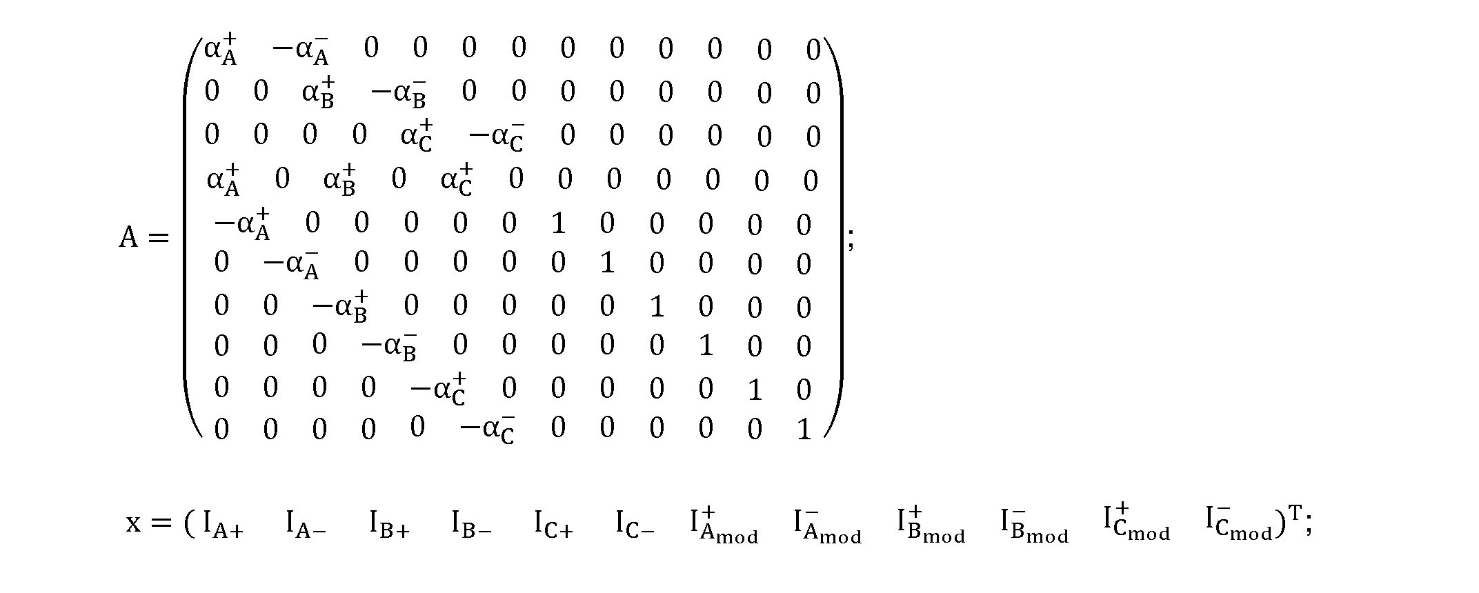

Other equivalent converter configurations and corresponding analysis techniques are, however, also possible.
Optionally, the controller 32 may also be programmed to carry out mathematical optimization by applying a current weighting to the relative current contribution provided by each limb portion 12A+, 12A-, 12B+, 12B-, 12C+, 12C-. The respective current weighting for each limb portion 12A+, 12A-, 12B+, 12B-, 12C+, 12C- may be determined according to measured operating parameters of the converter 10 during its operation. The various current weightings can be determined throughout operation of the said converter 10 so as to permit an updating of the current weightings, e.g. in response to changing environmental conditions. As a result the various current weightings can vary as the converter 10 operates. Preferably during normal operation of the converter 10 an identical current weighting is applied to each limb portion current

However, when the converter 10 is operating under certain conditions, e.g. an abnormal operating condition, a different current weighting may be applied to the current contribution, i.e. the limb portion current

provided by at least one limb portion 12A+, 12A-, 12B+, 12B-, 12C+, 12C-. For example, a larger current weighting may be applied to the optimal limb portion current that a particular limb portion 12A+, 12A-, 12B+,

12B-, 12C+, 12C must contribute, so as to reduce an actual limb portion current that the said limb portion contributes relative to an actual current contribution of each of the other limb portions, which are otherwise all the same as one another.
Returning to the embodiment described hereinabove, the controller 32 is programmed to carry out mathematical optimization to determine a minimum individual limb portion current that each of the limb portion 12A+, 12A-,

12B+, 12B-, 12C+, 12C- must contribute so as to track the corresponding required AC current demand phase waveform C and the required DC current demand be, i.e.


as individual current references with which the corresponding actual measured limb portion currents can be compared in order to, via some subsequent control action, reduce the error between the reference and measured current values. One way in which minimum individual limb portion currents

the unknown elements of x in the equation set out above, may
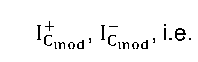

be determined is by solving a nonlinear optimization of the general form:

subject to the equality constrained equation of the form:
A. x = b where is the current objective function to be minimized;

Ψ is the current weighting at time ti ; f is the current cost function which may optionally include a current weighting matrix
x is the transpose of

reflected in a column vector;
 t0 is the time at which a particular period of control of the converter 10 starts; and t is the time at which a particular period of control of the converter 10 ends. As mentioned above, the current weighting matrix Ql may be determined according to measured operating parameters of the converter 10, and may be so determined throughout the operation of the converter 10, such that it can vary as the said converter 10 is controlled in response to changes in the operation of the converter 10.
Meanwhile one example of a current objective function to be minimized is
t0 is the time at which a particular period of control of the converter 10 starts; and t is the time at which a particular period of control of the converter 10 ends. As mentioned above, the current weighting matrix Ql may be determined according to measured operating parameters of the converter 10, and may be so determined throughout the operation of the converter 10, such that it can vary as the said converter 10 is controlled in response to changes in the operation of the converter 10.
Meanwhile one example of a current objective function to be minimized is


where the current objective function, i.e. J(x), is minimised subject to the equality constraints expressed as linear equations above, with
 being the transpose of the vector x set out above.
When subject only to an equality constrained equation, as mentioned above, the Lagrangian (or the method of Lagrange multipliers) is a technique for solving the above-identified nonlinear optimization in order to find local minima of the current objective function It may also be solved using other optimization algorithms,

including iterative and programming algorithms.
As a general optimal control problem, the aforementioned nonlinear optimization could additionally include one or more inequality constraints in which case it could be solved by using the further method of Hamiltonian (Pontryagin's minimum principle).
One example of such an inequality constraint is:

where
C is a matrix which maps possible maximum current flow paths provided by the limb portions 12A+, 12A-, 12B+, 12B-, 12C+, 12C-; and
d is a vector representing of the maximum desired current in each limb portion 12A+, 12A-, 12B+, 12B-, 12C+, 12C-.
In either case the minimum individual limb portion currents

may also be determined by solving a nonlinear optimization of the form


Thereafter the controller 32 is still further programmed to apply a feedback control algorithm to directly establish limb portion voltage sources

necessary to provide the determined minimum individual limb portion current


12C- must contribute.
Claims
1 . A voltage source converter (10), for use in high voltage direct current power transmission and distribution, comprising: a plurality of converter limbs (12A, 12B, 12C) corresponding to respective phases of the voltage source converter (10), each converter limb (12A, 12B, 12C) extending between first and second DC terminals (14, 16) and including first and second limb portions (12A+, 12A-, 12B+, 12B-, 12C+, 12C-) separated by an AC terminal, each limb portion including a chain-link converter (24A+, 24A-, 24B+, 24B-, 24C+, 24C-) operable to provide a stepped variable voltage source and a primary switching element (Sw1, Sw2, Sw3, Sw4, Sw5, Sw6) selectively operable in a conducting mode in which current is able to flow therethrough and a non-conducting mode in which current is unable to flow therethrough, each converter limb (12A, 12B, 12C) being selectively operable in a fully-conducting mode in which the primary switching element (Sw1, Sw2, Sw3, Sw4, Sw5, Sw6) in each limb portion (12A+, 12A-, 12B+, 12B-, 12C+, 12C-) thereof operates in its conducting mode and a partially-conducting mode in which the primary switching element (Sw1, Sw2, Sw3, Sw4, Sw5, Sw6) in one limb portion thereof operates in its conducting mode and the primary switching element (Sw1, Sw2, Sw3, Sw4, Sw5, Sw6) in the other limb portion thereof operates in its non-conducting mode; and a controller (32) programmed to transition a given converter limb (12A, 12B, 12C) from its fully-conducting mode to its partially-conducting mode by:
(a) transitioning another converter limb (12A, 12B, 12C) from its partially- conducting mode to its fully-conducting mode while the given converter limb (12A, 12B, 12C) to be transitioned from its fully-conducting mode to its partially-conducting mode remains in its fully-conducting mode; and
(b) circulating a commutation current around a commutation loop (40) defined by the converter limb (12A, 12B, 12C) transitioned into its fully-conducting mode and the converter limb remaining in its fully-conducting mode to facilitate the switching into its non-conducting mode of a primary switching element (Sw1, Sw2, Sw3, Sw4, Sw5, Sw6) in the given converter limb (12A, 12B, 12C) to be transitioned into its partially-conducting mode.
2. A voltage source converter according to Claim 1 , wherein: each primary switching element (Sw1 , Sw2 , Sw3 , Sw4, Sw5, Sw6 ) includes a director switch (28+, 28-) selectively openable and closeable to respectively prevent and allow the flow of current therethrough and an anti-parallel diode electrically connected in anti-parallel with the director switch (28+, 28-); and the controller (32) is programmed to circulate a commutation current around the commutation loop (40) to drive to zero the current flowing through an anti-parallel diode (30+, 30-) of the primary switching element (Sw1 , Sw2 , Sw3 , Sw4, Sw5, Sw6 ) to be switched into its non-conducting mode.
3. A voltage source converter according to Claim 2, wherein prior to circulating a commutation current around the commutation loop (40) the controller (32) is programmed to establish whether current is flowing through the anti-parallel diode (30+, 30-) of the primary switching element (Sw1 , Sw2 , Sw3 , Sw4, Sw5, Sw6) to be switched into its non-conducting mode and, if current is not flowing through the said anti-parallel diode (30+, 30-), the controller (32) is programmed to: circulate an initiating commutation current around the commutation loop (40) to cause the said anti-parallel diode (30+, 30-) to begin conducting; establish that the said anti-parallel diode (30+, 30-) is conducting current; and open the director switch (28+, 28-) in the said primary switching element (Sw1 , Sw2 , Sw3 , Sw4, Sw5, Sw6) to be switched into its non-conducting mode while the said anti-parallel diode (30+, 30-) is conducting current.
4. A voltage source converter according to Claim 3, wherein the controller (32) is additionally programmed to control the initiating commutation current to drive to zero the current flowing through the said anti-parallel diode (30+, 30-).
5. A voltage source converter according to any of Claims 2 to 4, wherein prior to circulating a commutation current around the commutation loop (40) the controller (32) is programmed to establish whether current is flowing through the anti-parallel diode (30+, 30-) of the primary switching element (Sw1 , Sw2 , Sw3 , Sw4, Sw5, Sw6 ) to be switched into its non-conducting mode and, if current is flowing through the said anti- parallel diode (30+, 30-), the controller (32) is programmed to open the director switch
(28+, 28-) in the said primary switching element (Sw1 , Sw2 , Sw3 , Sw4, Sw5, Sw6 ) to be switched into its non-conducting mode.
6. A voltage source converter according to Claim 5, wherein after opening the director switch (28+, 28-) of the primary switching element (Sw1 , Sw2 , Sw3 , Sw4, Sw5, Sw6 ) to be switched into its non-conducting mode the controller (32) is programmed to circulate an extinguishing commutation current around the commutation loop (40) to drive to zero the current flowing through the said anti-parallel diode (30+, 30-).
7. A voltage source converter according to Claim 4 or Claim 6, wherein the controller (32) is further programmed to impose a reverse bias voltage across the said anti-parallel diode (30+, 30-) to maintain it in a reverse-biased non-conducting condition.
8. A voltage source converter according to any of Claims 3 to 7, wherein establishing whether current is flowing through the said anti-parallel diode (30+, 30-) includes observing the polarity of the voltage across the primary switching element (Sw1 , Sw2 , Sw3 , Sw4, Sw5, Sw6 ) to be switched into its non-conducting mode.
9. A voltage source converter according to Claim 8, wherein the controller (32) includes a control sub-unit configured to determine from the observation of voltage polarity across the primary switching element (Sw1 , Sw2 , Sw3 , Sw4, Sw5, Sw6 ) to be switched into its non-conducting mode the direction of current flow through the said primary switching element (Sw1 , Sw2 , Sw3 , Sw4, Sw5, Sw6 ).
10. A voltage source converter according to any preceding claim, wherein the controller (32) is still further programmed to: obtain a respective AC current demand phase waveform for each converter limb which the corresponding converter limb (12A, 12B, 12C) is required to track, and a DC current demand which each converter limb (12A, 12B, 12C) is also required to track; and carry out mathematical optimization to determine for each limb portion (12A+, 12A-, 12B+, 12B-, 12C+, 12C-) an optimal limb portion current which as necessary includes a commutation current component and which the limb portion (12A+, 12A-,
12B+, 12B-, 12C+, 12C-) must contribute to track the corresponding required AC current demand phase waveform and the required DC current demand.
1 1 . A voltage source converter according to Claim 10, wherein the controller (32) is programmed to carry out mathematical optimization by considering an equivalent converter configuration (100) which represents the flow of current through the voltage source converter (10).
12. A voltage source converter according to Claim 1 1 , wherein the controller (32) is programmed to consider an equivalent converter configuration (100) which represents the flow of current through the voltage source converter (10) by mapping possible current flow paths through the converter (10).
13. A voltage source converter according to any of Claims 10 to 12, wherein the controller (32) is programmed to carry out mathematical optimization to determine one or more minimum individual limb portion currents that the corresponding limb portion (12A+, 12A-, 12B+, 12B-, 12C+, 12C-) must contribute to track the corresponding required AC current demand phase waveform and the required DC current demand.
Applications Claiming Priority (2)
| Application Number | Priority Date | Filing Date | Title |
|---|---|---|---|
| GB1604069.3 | 2016-03-09 | ||
| GB1604069.3A GB2548133B (en) | 2016-03-09 | 2016-03-09 | A voltage source converter for use in high voltage direct current power transmission |
Publications (1)
| Publication Number | Publication Date |
|---|---|
| WO2017153553A1 true WO2017153553A1 (en) | 2017-09-14 |
Family
ID=55859242
Family Applications (1)
| Application Number | Title | Priority Date | Filing Date |
|---|---|---|---|
| PCT/EP2017/055618 Ceased WO2017153553A1 (en) | 2016-03-09 | 2017-03-09 | Commutation pattern for director switches in hybrid modular multilevel converter |
Country Status (2)
| Country | Link |
|---|---|
| GB (1) | GB2548133B (en) |
| WO (1) | WO2017153553A1 (en) |
Cited By (2)
| Publication number | Priority date | Publication date | Assignee | Title |
|---|---|---|---|---|
| CN107846036A (en) * | 2017-11-02 | 2018-03-27 | 南方电网科学研究院有限责任公司 | High voltage flexible direct current transmission system and its main circuit equipment determination method |
| US20180166966A1 (en) * | 2015-05-28 | 2018-06-14 | General Electric Technology Gmbh | Improvements in or relating to the control of voltage source converters |
Family Cites Families (2)
| Publication number | Priority date | Publication date | Assignee | Title |
|---|---|---|---|---|
| EP2650999A3 (en) * | 2010-04-08 | 2015-11-04 | Alstom Technology Ltd | Multi module voltage source converter for a HVDC system |
| CN103283140B (en) * | 2010-10-27 | 2015-07-29 | 阿尔斯通技术有限公司 | Modular multilevel converter |
-
2016
- 2016-03-09 GB GB1604069.3A patent/GB2548133B/en not_active Expired - Fee Related
-
2017
- 2017-03-09 WO PCT/EP2017/055618 patent/WO2017153553A1/en not_active Ceased
Non-Patent Citations (3)
| Title |
|---|
| FAN BORAN ET AL: "Module-capacitor voltage fluctuation optimization control for an alternate arm converter", 2015 IEEE ENERGY CONVERSION CONGRESS AND EXPOSITION (ECCE), IEEE, 20 September 2015 (2015-09-20), pages 3326 - 3330, XP032801065, DOI: 10.1109/ECCE.2015.7310129 * |
| J.C. CLARE ET AL: "Alternate Arm Converter (AAC) operation under faulted AC-grid conditions", 7TH IET INTERNATIONAL CONFERENCE ON POWER ELECTRONICS, MACHINES AND DRIVES (PEMD 2014), 1 January 2014 (2014-01-01), pages 0243 - 0243, XP055374500, ISBN: 978-1-84919-815-8, DOI: 10.1049/cp.2014.0358 * |
| NAJMI VAHID ET AL: "Design and control of modular multilevel alternate arm converter (AAC) with Zero Current Switching of director switches", 2015 IEEE ENERGY CONVERSION CONGRESS AND EXPOSITION (ECCE), IEEE, 20 September 2015 (2015-09-20), pages 6790 - 6797, XP032801546, DOI: 10.1109/ECCE.2015.7310610 * |
Cited By (2)
| Publication number | Priority date | Publication date | Assignee | Title |
|---|---|---|---|---|
| US20180166966A1 (en) * | 2015-05-28 | 2018-06-14 | General Electric Technology Gmbh | Improvements in or relating to the control of voltage source converters |
| CN107846036A (en) * | 2017-11-02 | 2018-03-27 | 南方电网科学研究院有限责任公司 | High voltage flexible direct current transmission system and its main circuit equipment determination method |
Also Published As
| Publication number | Publication date |
|---|---|
| GB201604069D0 (en) | 2016-04-20 |
| GB2548133A (en) | 2017-09-13 |
| GB2548133B (en) | 2018-10-10 |
Similar Documents
| Publication | Publication Date | Title |
|---|---|---|
| EP2863534B1 (en) | Voltage source converter | |
| US9312705B2 (en) | Capacitor balancing circuit and control method for an electronic device such as a multilevel power inverter | |
| US9325252B2 (en) | Multilevel converter systems and sinusoidal pulse width modulation methods | |
| EP2883069B1 (en) | Method and device for controlling a multilevel converter | |
| US8929111B2 (en) | System and method for common-mode elimination in a multi-level converter | |
| Norambuena et al. | A method to eliminate steady-state error of model predictive control in power electronics | |
| CA2877440C (en) | Controlling a modular converter | |
| US9007787B2 (en) | Method and apparatus for bypassing Cascaded H-Bridge (CHB) power cells and power sub cell for multilevel inverter | |
| JP6529676B2 (en) | Active discharge of a modular multilevel converter | |
| CN107852107B (en) | Electric energy converter | |
| EP3096446A1 (en) | A method of controlling a converter | |
| JP6779424B1 (en) | Power converter | |
| US20160329833A1 (en) | Improvements in or relating to converters for use in high voltage direct current power transmission | |
| Xu et al. | Open-loop voltage balancing algorithm for two-port full-bridge MMC-HVDC system | |
| WO2018100051A1 (en) | Improvements in or relating to hvdc power converters | |
| WO2017153553A1 (en) | Commutation pattern for director switches in hybrid modular multilevel converter | |
| EP3063866B1 (en) | A vector controller for a voltage source power converter | |
| Hussein et al. | Cascaded multioutput multilevel converter: Modulation and operating limits | |
| US20180233916A1 (en) | Voltage source converter | |
| Cortes et al. | Predictive control of a grid-connected cascaded H-bridge multilevel converter | |
| US11121640B2 (en) | Systems, methods, and apparatus for controlling a voltage source converter | |
| JP2022056359A (en) | Power conversion apparatus | |
| US12003169B2 (en) | Chain-link modules for voltage source converters | |
| WO2024017962A1 (en) | Improvements in or relating to power transmission networks | |
| Verne et al. | Predictive direct torque control using a cascade asymmetric multilevel converter |
Legal Events
| Date | Code | Title | Description |
|---|---|---|---|
| NENP | Non-entry into the national phase |
Ref country code: DE |
|
| 121 | Ep: the epo has been informed by wipo that ep was designated in this application |
Ref document number: 17709966 Country of ref document: EP Kind code of ref document: A1 |
|
| 122 | Ep: pct application non-entry in european phase |
Ref document number: 17709966 Country of ref document: EP Kind code of ref document: A1 |