WO2017138032A1 - Time-of-flight distance measuring device and method for detecting multipath error - Google Patents
Time-of-flight distance measuring device and method for detecting multipath error Download PDFInfo
- Publication number
- WO2017138032A1 WO2017138032A1 PCT/JP2016/000638 JP2016000638W WO2017138032A1 WO 2017138032 A1 WO2017138032 A1 WO 2017138032A1 JP 2016000638 W JP2016000638 W JP 2016000638W WO 2017138032 A1 WO2017138032 A1 WO 2017138032A1
- Authority
- WO
- WIPO (PCT)
- Prior art keywords
- signals
- switch
- photodetectors
- different types
- subset
- Prior art date
- Legal status (The legal status is an assumption and is not a legal conclusion. Google has not performed a legal analysis and makes no representation as to the accuracy of the status listed.)
- Ceased
Links
Images











Classifications
-
- G—PHYSICS
- G01—MEASURING; TESTING
- G01S—RADIO DIRECTION-FINDING; RADIO NAVIGATION; DETERMINING DISTANCE OR VELOCITY BY USE OF RADIO WAVES; LOCATING OR PRESENCE-DETECTING BY USE OF THE REFLECTION OR RERADIATION OF RADIO WAVES; ANALOGOUS ARRANGEMENTS USING OTHER WAVES
- G01S7/00—Details of systems according to groups G01S13/00, G01S15/00, G01S17/00
- G01S7/48—Details of systems according to groups G01S13/00, G01S15/00, G01S17/00 of systems according to group G01S17/00
- G01S7/497—Means for monitoring or calibrating
-
- G—PHYSICS
- G01—MEASURING; TESTING
- G01S—RADIO DIRECTION-FINDING; RADIO NAVIGATION; DETERMINING DISTANCE OR VELOCITY BY USE OF RADIO WAVES; LOCATING OR PRESENCE-DETECTING BY USE OF THE REFLECTION OR RERADIATION OF RADIO WAVES; ANALOGOUS ARRANGEMENTS USING OTHER WAVES
- G01S17/00—Systems using the reflection or reradiation of electromagnetic waves other than radio waves, e.g. lidar systems
- G01S17/02—Systems using the reflection of electromagnetic waves other than radio waves
- G01S17/06—Systems determining position data of a target
- G01S17/08—Systems determining position data of a target for measuring distance only
- G01S17/32—Systems determining position data of a target for measuring distance only using transmission of continuous waves, whether amplitude-, frequency-, or phase-modulated, or unmodulated
- G01S17/36—Systems determining position data of a target for measuring distance only using transmission of continuous waves, whether amplitude-, frequency-, or phase-modulated, or unmodulated with phase comparison between the received signal and the contemporaneously transmitted signal
-
- G—PHYSICS
- G01—MEASURING; TESTING
- G01S—RADIO DIRECTION-FINDING; RADIO NAVIGATION; DETERMINING DISTANCE OR VELOCITY BY USE OF RADIO WAVES; LOCATING OR PRESENCE-DETECTING BY USE OF THE REFLECTION OR RERADIATION OF RADIO WAVES; ANALOGOUS ARRANGEMENTS USING OTHER WAVES
- G01S17/00—Systems using the reflection or reradiation of electromagnetic waves other than radio waves, e.g. lidar systems
- G01S17/88—Lidar systems specially adapted for specific applications
- G01S17/89—Lidar systems specially adapted for specific applications for mapping or imaging
- G01S17/894—Three-dimensional [3D] imaging with simultaneous measurement of time-of-flight at a two-dimensional [2D] array of receiver pixels, e.g. time-of-flight cameras or flash lidar
-
- G—PHYSICS
- G01—MEASURING; TESTING
- G01S—RADIO DIRECTION-FINDING; RADIO NAVIGATION; DETERMINING DISTANCE OR VELOCITY BY USE OF RADIO WAVES; LOCATING OR PRESENCE-DETECTING BY USE OF THE REFLECTION OR RERADIATION OF RADIO WAVES; ANALOGOUS ARRANGEMENTS USING OTHER WAVES
- G01S7/00—Details of systems according to groups G01S13/00, G01S15/00, G01S17/00
- G01S7/48—Details of systems according to groups G01S13/00, G01S15/00, G01S17/00 of systems according to group G01S17/00
- G01S7/491—Details of non-pulse systems
- G01S7/4911—Transmitters
-
- G—PHYSICS
- G01—MEASURING; TESTING
- G01S—RADIO DIRECTION-FINDING; RADIO NAVIGATION; DETERMINING DISTANCE OR VELOCITY BY USE OF RADIO WAVES; LOCATING OR PRESENCE-DETECTING BY USE OF THE REFLECTION OR RERADIATION OF RADIO WAVES; ANALOGOUS ARRANGEMENTS USING OTHER WAVES
- G01S7/00—Details of systems according to groups G01S13/00, G01S15/00, G01S17/00
- G01S7/48—Details of systems according to groups G01S13/00, G01S15/00, G01S17/00 of systems according to group G01S17/00
- G01S7/491—Details of non-pulse systems
- G01S7/4912—Receivers
- G01S7/4915—Time delay measurement, e.g. operational details for pixel components; Phase measurement
Definitions
- the present disclosure relates to a time-of-flight distance measuring device and a method for detecting a multipath error.
- a time-of-flight (TOF) technology As a method for measuring the distance to an object in a scene, a time-of-flight (TOF) technology has been developed.
- TOF technology may be used in a variety of fields, such as automotive industries, human-interfaces and gaming, robotics or the like.
- the TOF technology works by illuminating a scene with modulated light emitted from a light source and by observing reflected light reflected by an object in the scene. By measuring the phase difference between the emitted light and the reflected light, the distance to the object is calculated (see, e.g., Patent Literatures 1 to 4).
- multipath interference may affect the accuracy of the measured distance.
- the multipath interference arises when the emitted light travels along multiple paths that have a different path length from each other and then is sensed by a single photo receiver as integrated light. Although the phases of light along the different path lengths are different each other, the conventional distance measuring device computes a distance based on mixed phases of the integrated light. Therefore, the computed distance may include an error value arising from the multipath interference.
- the objective of the present disclosure is to provide a time-of-flight distance measuring device and a method for detecting a multipath error that may estimate an error value associated with a multipath error without a time lag or with a reduced time lag.
- a time-of-flight distance measuring device includes (i) a light source that emits light, as emitted light, toward an object, (ii) a light receiver that includes a plurality of photodetectors, the light receiver detecting, as reflected light, the emitted light reflected by the object, (iii) a first controller that controls the light source to emit the emitted light as an amplitude-modulated waveform such that the emitted light includes a fundamental component at a fundamental frequency and at least one harmonic component of the fundamental frequency, (iv) a second controller that generates a plurality of control signals and outputs each of the plurality of control signals to a respective one of the plurality of photodetectors, (v) a calculator that calculates amplitudes and phase angles of the fundamental component and the at least one harmonic component based on a detection value of the light receiver, and (vi) an error estimator that estimates an error value associated with a multipath error based on the amplitude
- the second controller generates the plurality of controls signals to simultaneously sense the fundamental component and the at least one harmonic component.
- the time-of-flight distance measuring device may estimate an error value due to a multipath error with high accuracy.
- a method for detecting a multipath error using a time-of-flight distance measuring technology includes (i) emitting light, as emitted light, from a light source toward an object, (ii) detecting, as detected light, the emitted light reflected by the object by a light receiver, the light receiver including a plurality of photodetectors, (iii) controlling the light source to emit the emitted light as an amplitude-modulated waveform such that the emitted light includes a fundamental component at a fundamental frequency and at least one harmonic component of the fundamental frequency, (iv) generating a plurality of control signals and outputting each of the plurality of control signals to a respective one of the plurality of photodetectors, (v) calculating amplitudes and phase angles of the fundamental component and the at least one harmonic component based on a detection value of the light receiver, and (vi) estimating an error value associated with a multipath error based on the amplitudes and the phase angles calculated by
- the plurality of controls signals is generated to simultaneously sense the fundamental component and the at least one harmonic component.
- the method for detecting a multipath error may estimate an error value due to a multipath error with high accuracy.
- Figure 1 is an explanatory model where multipath interference occurs (Fig. 1(a)) and the multipath interference is resolved (Fig. 1(b)).
- Figure 2 is a schematic view of a time-of-flight distance measuring device according to a first embodiment.
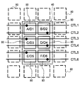
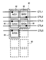
- Figure 3 is a plan view of pixel sensors according to the first embodiment.
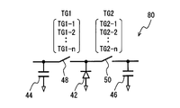
- Figure 4 is a schematic view of the pixel sensor according to the first embodiment.
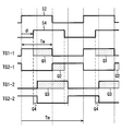
- Figure 5 is one example of a signal sequence for one pixel sensor.
- Figure 6 is one example of a differential signal sequence for one pixel sensor.
- Figure 7 is emitted light at a 25% duty cycle according to the first embodiment.
- Figure 8 is a graph showing a relation between amplitude and a duty cycle for a fundamental component, a second harmonic component and a third harmonic component.
- Figure 9 is one example of a control signal according to the first embodiment.
- Figure 10 is a schematic view of one pixel sensor when the pixel sensor is in a third state.
- Figure 11 is the differential sequence of the control signals according to the first embodiment.
- Figure 12 is a comparative view of a sampling sequence according to the first embodiment and a comparative example.
- Figure 13 is a schematic view of a processing unit according to the first embodiment.
- Figure 14 is a schematic view illustrating a mechanism of generating mixed light.
- Figure 15 is a graph showing a relation between a multipath error and a path length difference (Fig.
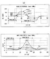
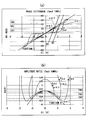
- Figure 16 is a graph showing the relation between the phase difference and the path length difference at a reflection rate of 0.3, 0.5 and 0.7 (Fig. 16(a)) and the relation between the amplitude ratio and the path length difference at the reflection rate of 0.3, 0.5 and 0.7 (Fig. 16(b)).
- Figure 17 is a graph showing a relation between the phase difference and an error value at the reflection rate of 0.3, 0.5 and 0.7 (Fig.
- Figure 18 is a flowchart showing a process to estimate the error value according to the first embodiment.
- Figure 19 is a schematic view of one pixel sensor when the pixel sensor is in the third state according to a second embodiment.
- Figure 20 is a schematic view of the pixel sensors according to a third embodiment.
- Figure 21 is a comparative view of the sampling sequence according to a fourth embodiment and a comparative example.
- Figure 22 is a schematic view of the processing unit according to the fourth embodiment.
- Figure 23 is a schematic view of the pixel sensors according to a fifth embodiment.
- Figure 24 is a comparative view of the sampling sequence according to the fifth embodiment and a comparative example.
- Figure 25 is a schematic view of the pixel sensors according to a sixth embodiment.
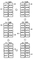
- Figure 26 is a schematic view of the pixel sensors according to a seventh embodiment.
- Figure 27 is a graph showing the relation between the phase difference and the path length difference at a reflection rate of 0.3, 0.5 and 0.7 (Fig. 27(a)) and the relation between the amplitude ratio and the path length difference at the reflection rate of 0.3, 0.5 and 0.7 (Fig. 27(b)).
- Figure 28 is a graph showing the relation between the phase difference and the error value at the reflection rate of 0.3, 0.5 and 0.7 (Fig.
- Figure 29 is a flowchart showing a process to estimate the error value according to the eighth embodiment.
- Figure 30 is a schematic view of the processing unit according to a ninth embodiment.
- Figure 31 is a flowchart showing a process to determine a foggy condition according to the ninth embodiment.
- Fig. 1(a) shows an explanatory model where multipath interference arises.
- a distance measuring device 10 as a comparative example to the present disclosure, is used to calculate a distance to an object (e.g., a pedestrian) 12 in a scene.
- the distance measuring device (hereinafter "comparative device") 10 emits light from a light source 14 and receives the light reflected by the object with a light receiver 16.
- a first path indicated by the solid line shows a direct path where the light emitted from the light source 14 directly reaches, and is reflected by, the object 12 and returns to the light receiver 16.
- a second path indicated broken line shows a multi-reflected path where the light emitted from the light source 14 is reflected first by an intermediate object, such as a vehicle, 18 and then the light is reflected by the object 12.
- the path length along the multi-reflected path can be represented as d+ ⁇ d.
- the comparative device 10 calculates a distance value L+ ⁇ L, where L is a distance value arising from d and an error value ⁇ L arising from ⁇ d. If the multipath error does not occur, the distance value L is nearly equal to the actual path length d.
- the comparative device 10 sequentially emits the light with different frequencies.
- the light source 14 emits the light with a first frequency f1 (e.g., 10MHz) for a predetermined period (e.g., 10msec) at a first timing, and then the light source 14 emits the light with a second frequency f2 (e.g., 20MHz) for the same period at a second timing. Therefore, it takes, in total, at least two predetermined periods (i.e., 20msec) for the comparative device 10 to detect the multipath error. In other words, a time lag due to the sequential emission of light is inevitably generated in the comparative example 10.
- the distance value calculated by the comparative device 10 may still include an error in a situation described below.
- a multipath arises during the measurement with the first frequency f1
- the multipath error is resolved when the intermediate object 18 moves away from the scene during the measurement with the second frequency f2 as shown in Fig. 1(b).
- the comparative device 10 obtains information affected by the multipath interference for the light with the first frequency f1, and then obtains information without the multipath interference for the light with the second frequency f2. Therefore, the comparative device calculates the error value using both the information affected by the multipath interference and the information not affected by the multipath interference. As a result, the error value of the multipath error calculated by the comparative device 10 may still be inaccurate.
- the inventors of the present disclosure here present a plurality of embodiments of the time-of-flight distance measuring device that may detect a multipath error without a time lag or with a reduced time lag.
- the time-of-flight distance measuring device (hereinafter, collectively "TOF device") is used in a vehicle to calculate a distance to an object from the vehicle (i.e., the TOF device), but the usage of the TOF device is not limited to a vehicle.
- the TOF device may be used for human-interface devices, gaming consoles, robots or the like.
- the "object" for the TOF device may include a pedestrian, other vehicles, obstacles on a road, buildings or the like.
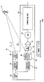
- FIG. 2 is a block diagram illustrating a general configuration of the TOF device 20 according to the first embodiment.
- the TOF device 20 includes a clock generator 22, a light source 24, a light receiver 26, an emitter controller (first controller) 28, a receiver controller (second controller) 30, a common-mode choke 32, a differential amplifier 34, an A/D converter 36 and a processing unit 38.
- the clock generator 22 generates and outputs a clock signal to both the emitter controller 28 and the receiver controller 30 to establish synchronization between the light source 24 and the light receiver 26.
- the emitter controller 28 and the receiver controller 30 On receiving the clock signal from the clock generator 22, the emitter controller 28 and the receiver controller 30 generate and output a variety of signals to the light source 24 and the light receiver 26, respectively, to work in synchronism with each other.
- the emitter controller 28 When the emitter controller 28 receives the clock signal from the clock generator 22, the emitter controller 28 outputs a square wave as an emission control signal to the light source 24.
- the light source 24 emits light, as emitted light, with a square waveform (i.e., an amplitude-modulated waveform) corresponding to the emission control signal.
- the emitted light has a same waveform as the emission control signal.
- the light source 24 may emit light having a sine waveform, a triangle waveform, or a waveform with a pseudo random pattern.
- the light source 24 is a light emitting diode (LED) that emits infrared light toward the object 12.
- a laser diode (LD) that emits infrared light may be used as the light source 24.
- the emitter controller 28 controls the light source 24 such that the emitted light includes a fundamental component at a fundamental frequency and at least one harmonic component of the fundamental frequency.
- the emitted light includes the fundamental component (i.e., first-order component) at the fundamental frequency (e.g., 10MHz) and a second harmonic component (i.e., second-order component) at two times the fundamental frequency (e.g., 20MHz).
- the emitted light with the fundamental component and the second harmonic component is emitted from the single light source 24.
- the emitted light may include the fundamental component and two other harmonic components, such as the second and third harmonic components.
- the emitted light may include the fundamental component and another harmonic component other than the second harmonic component, such as the third harmonic, the fourth harmonic, or the like.
- the receiver controller 30 generates and outputs a plurality of control signals (e.g., see D 1 to D 6 in Fig. 11) to the light receiver 26 to control a light receiving pattern of the light receiver 26.
- the receiver controller 30 generates the control signals D N such that the light receiver 26 simultaneously senses the fundamental component and the second harmonic component of the emitted light reflected by the object 12, as will be described later.
- the light receiver 26 detects, as reflected light, the emitted light reflected by the object 12 in the scene.
- the light receiver 26 includes a plurality of pixel sensors (photodetectors) 80 that are arranged in a regular array form.
- the plurality of pixel sensors 80 are grouped into a plurality of sensing units 40 and each sensing unit 40 is formed of six pixel sensors (subset of M photodetectors) 80.
- the pixel sensors 80 forming one sensing unit 40 may be also referred to as the pixel sensors A to F in place of the reference numeral "80".
- the receiver controller 30 controls each sensing unit 40 as a single unit.
- the receiver controller 30 outputs each of the plurality of control signals D N to a respective one of the plurality of pixel sensors A to F through wiring CTL1 to CTL6.
- each control signal D N is a differential signal including a pair of normally complimentary gate signals TG1, TG2.
- the pixel sensor 80 is an image sensor using CMOS (Complementary Metal Oxide Semiconductor) technology, CCD (Charge Coupled Device) technology, or combination of both the technologies.
- CMOS Complementary Metal Oxide Semiconductor
- CCD Charge Coupled Device
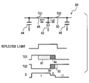
- each pixel sensor 80 includes a PD (photo diode, photo element) 42, a first capacitor 44, a second capacitor 46, a first switch 48 and a second switch 50.
- the first switch 48 and the second switch 50 are a MOS-type device, such as a MOS transistor or a transfer gate, or a charge-coupled device (CCD).
- the first capacitor 44 and the second capacitor 46 are a capacitive element, such as MOS, CCD or MIM (Metal Insulator Metal).
- the first capacitor 44 is electrically connected to the first switch 48, and the first switch 48 is electrically connected to the PD 42, and therefore the first capacitor 44 is electrically connected to the PD 42 through the first switch 48.
- the second capacitor 46 is electrically connected to the second switch 50 and the second switch 50 is electrically connected to the PD 42, and therefore the second capacitor 46 is electrically connected to the PD 42 through the second switch 50.
- the PD 42 generates electricity while being exposed to the reflected light.
- the control signal D N received from the receiver controller 30 operates the pixel sensor 80 by controlling an on/off state of the first switch 48 and the second switch 50.
- the control signal D N includes a pair of gate signals TG1, TG2 that are normally complimentary
- the first capacitor 44 stores electric charge generated from the PD 42.
- the second capacitor 46 stores electric charge generated from the PD 42.
- first switch 48 and the first capacitor 44, and the second switch 50 and the second capacitor 46 are used in the present embodiment, three or more pairs of a switch and a capacitor may be used.
- the electric charge stored in the first capacitor 44 and the electric charge stored in the second capacitor 46 are separately output to the common-mode choke 32 as analog data.
- the common-mode choke 32 is used to avoid light saturation by removing common mode (CM) components from the data output from the pixel sensor 80.
- CM common mode
- the CM components are generated when light saturation occurs, i.e., when sufficiently high background light exists in the scene.
- the differential amplifier 34 After removing the CM component, the data corresponding to the first capacitor 44 and the data corresponding to the second capacitor 46 are input into the differential amplifier 34.
- the differential amplifier 34 outputs the difference value between each pair of the electric charge data to the A/D converter 36. That is, the difference value between the data corresponding to the electric charge stored in the first capacitor 44 and the data corresponding to the electric charge stored in the second capacitor 46 are output from the differential amplifier 34.
- the A/D converter 36 converts the analog data from the differential amplifier 34 to digital data and outputs the digital data to the processing unit 38.
- the processing unit 38 includes a CPU, a ROM, a RAM or the like, and performs programs stored in the ROM to execute a variety of processing. Especially, the processing unit 38 calculates the distance (a distance value L) to the object 12 based on the digital data output from the A/D converter 36. Further, the processing unit 38 estimates an error value ⁇ L due to a multipath error and corrects the distance based on the estimated error value ⁇ L.
- Fig. 5 shows one example of a signal sequence (modulation cycle: Tm, exposure period: Tw) where the emitted light has a 50% duty cycle and the pixel sensor 80 is controlled through the gate signalsTG1, TG2 having a different phase from each other.
- the pixel sensor 80 is first controlled through a first pair of gate signals TG1-1, TG2-1, and then is controlled through a second pair of gate signals TG1-2, TG2-2.
- the waveform (emitted light waveform 52) of the emitted light from the light source 24 is a square form in synchronism with the gate signals TG1, TG2.
- the waveform (reflected light waveform 54) of the reflected light has a time difference relative to the emitted light waveform 52, and thus the reflected light waveform 54 is sensed as a waveform having a phase delay with a phase difference ⁇ relative to the emitted light waveform 52.
- the first pair of gate signals TG1-1, TG2-1 has a phase difference of 180° from each other
- the second pair of gate signals TG1-2, TG2-2 has a phase difference of 180° from each other.
- the first pair of gate signals TG1-1, TG2-1 and the second pair of gate signals TG1-2, TG2-2 have a phase difference of 90° from each other.
- each gate signal TG1-1, TG2-1, TG1-2, TG2-2 is output for several to hundreds of thousands of cycles.
- the electric charges generated by the first pair of gate signals TG1-1, TG2-1 are obtained as data Q1, Q2, while the electric charges generated by the second pair gate signals TG1-2, TG2-2 are obtained as data Q3, Q4.
- the data is a voltage value that is a converted value of the electric charge through electric charge voltage conversion.
- the estimation value ⁇ of the phase difference ⁇ can be calculated by equation (1) using the discrete Fourier transform (DFT) with the data Q1 to Q4 obtained through the four samplings.
- DFT discrete Fourier transform
- equation (1) represents an equation when four samplings are executed
- the equation (1) can be generalized as to N phases (i.e., N samplings) as represented in equation (2).
- ⁇ tan -1 (( ⁇ Qk*sin(2 ⁇ /N*k)/( ⁇ Qk*cos(2 ⁇ /N*k))) (2)
- a distance to the object 12 can be calculated based on a relationship between ⁇ and the speed of light. It should be noted although these equations can be generally used to a distance to the object 12, the distance to the object 12 is calculated by using the phase angle of the fundamental component and the second harmonic component at the processing unit 38 in the first embodiment, as will be described below.
- the first pair of gate signals TG1-1, TG2-1 and the second pair of gate signals TG1-2, TG2-2 can be represented by respective differential signals D 1 , D 2 , as shown in Fig. 6.
- the differential signal D 1 , D 2 is an imaginary signal that indicates the state of the pair of gate signals TG1, TG2.
- the gate signals TG1, TG2 are normally complimentary.
- the differential signal D 1 , D 2 has a value of "1" when a first gate signal TG1 is "H” and a second gate signal TG2 is "L".
- the differential signal D 1 , D 2 has the value "1"
- the on/off state of the first switch 48 and the second switch 50 is a first state where the first switch 48 is on and the second switch 50 is off.
- the differential signal D 1 , D 2 has the value of "-1" when the first gate signal is “L” and the second gate signal is "H".
- the on/off state of the first switch 48 and the second switch 50 is a second state where the first switch 48 is off and the second switch 50 is on. Therefore, the state of the pair of gate signals TG1, TG2 (i.e., the on/off state of the first and second switches 48, 50) can be represented by a differential signal (control signal D N ) that is normally either "1" or "-1".
- the emitted light is emitted with a fundamental component and its second order harmonic component, which are reflected and then simultaneously sensed by the light receiver 26.
- the emitted light is emitted with a fundamental component and its second order harmonic at a duty cycle of less than 50% and (ii) the control signal is generated to be sensitive to the second harmonic component as well as the fundamental component.
- the emitter controller 28 in the present embodiment controls the light source 24 to emit the emitted light having a duty cycle of less than 50%.
- the emitted light may be emitted with a duty cycle of 25%.
- the second harmonic component can be effectively sensed as described below.
- Fig. 7 shows the emitted light 56 having a 25% duty cycle in the present embodiment indicated by the solid line and a comparative emitted light 58 having a 50% duty cycle indicated by the broken line.
- Fig. 8 shows a relation between amplitude and a duty cycle [%] for the fundamental component, the second harmonic component and the third harmonic component.
- the amplitude of the second harmonic component and the third harmonic component gradually increase as the duty cycle decreases from 50%.
- the amplitude of the second harmonic component has a maximum value at a duty cycle of 25%. Therefore, by setting the emitted light to have a 25% duty cycle in the present embodiment, the amplitude of the second harmonic component can be sensitively detected.
- the duty cycle is not limited to 25%.
- the amplitude of the second component and the third component are positive at duty cycles other than 25%. For example, if the emitted light includes the third harmonic component, the duty cycle may be set to, e.g., about 18% at which the third harmonic component has a maximum value.
- the receiver controller 30 generates each of the plurality of control signals D N to respective ones of the plurality of pixel sensors 80.
- the control signals D N are described as differential signals of the gate signals TG1, TG2 for the first switch 48 and the second switch 50 in the subsequent description, the differential signal is a representative signal that is physically implemented as a pair of normally complementary gate signals TG1, TG2 as explained previously..
- the control signal D N as shown in Fig. 9 in the present embodiment switches the on/off state of the first and the second switches 48, 50 between the first state indicated by "1" and the second state indicated by "-1".
- the receiver controller 30 Furthermore, to simultaneously sense the fundamental component and the second harmonic component of the reflected light, the receiver controller 30 generates the control signal D N to have a value of “0”, which represents a null period, as shown in Fig. 9. As described below, the data of the electric charge during the null period is cancelled. As a result, the electricity generated from the PD 42 during the null period is not used for calculating the distance value L or the error value ⁇ L at the subsequent process.
- the control signal D N has a value of “0” (i.e., the null period) when the first and second gate signals TG1, TG2, which are normally complimentary, are both set to be “H”.
- the control signal D N has the value "0”
- the on/off state of the first switch 48 and the second switch 50 is a third state where the first switch 48 is on and the second switch 50 is on
- the control signal D N is generated such that the third state occurs between the first state and the second state.
- the electricity generated from the PD 42 is evenly distributed to the first capacitor 44 and the second capacitor 46, and thus the first capacitor 44 stores the electric charge Qa and the second capacitor 46 stores the electric charge Qb that is equal to Qa during the third state (i.e., the null period). Therefore, the electric charges Qa and Qb stored during the third state are cancelled through the common-mode choke 32 and the differential amplifier 34, whereby the electric charges Qa and Qb are not used for calculating the distance value L and the error value ⁇ L at the processing unit 38.
- the data output from the differential amplifier 34 can include information associated with the second component as well as the fundamental component. In other words, the data associated with the fundamental component and the second component can be simultaneously obtained.
- the third state (the discharging state) is inserted from 1/2 ⁇ to 3/2 ⁇ phase (i.e., 90° to 270°) in one cycle of the control signal D N as shown in Fig. 9.
- one cycle of the control signal D N is formed of the first state ("1") from 0 to 1/2 ⁇ phase, the third state ("0") from 1/2 ⁇ to 3/2 ⁇ phase, and the second state ("-1") from 3/2 ⁇ to 2 ⁇ phase.
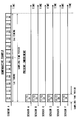
- Fig. 11 shows a differential signal sequence for one sensing unit 40 with 6 pixel sensors A to F in the present embodiment.
- the control signals are formed of 6 different types of signals D 1 to D 6 having a different phase from each other. More specifically, the signals D 1 to D 6 have a phase difference of, for example, 60° from each other.
- the receiver controller 30 outputs, at substantially the same time (specified timing), the 6 different types of signals D 1 to D 6 to the 6 pixel sensors A to F.
- the signals D 1 to D 6 are output for several hundreds to thousands of cycles.
- Each pixel sensor A to F receives a respective one of the 6 different signals D 1 to D 6 .
- each pixel sensor A to F in one sensing unit 40 is controlled by a different phase, and thus outputs electric charge data having a different value.
- the receiver controller 30 outputs the same subset of the 6 different types of signals D 1 to D 6 to each sensing unit 40.
- each sensing unit 40 is controlled to sense the reflected light with the same light sensing pattern as another sensing unit 40.
- the emitted light includes the fundamental component and the second harmonic component and has a 25% duty cycle. Further, the control signals are generated such that the light receiver 26 simultaneously senses the fundamental component and the second harmonic component.
- the data associated with the fundamental component and the second harmonic component can be obtained at substantially the same time. In other words, a sampling time period necessary for obtaining the data associated with the fundamental component and the second harmonic component can be shortened.
- Fig. 12 shows the sampling time period for obtaining the data of the fundamental component and the second harmonic component according to the present embodiment and a comparative example.
- the light source is controlled to emit the emitted light with the fundamental component indicated by "f1" in Fig. 12 (and light receiver is controlled to receive the reflected light) at a first timing, and then emit the emitted light with the second harmonic component indicated by "f2" in Fig. 12 (and receive the reflected light) at a second timing.
- the 6 different signals D 1 to D 6 are sequentially (i.e., not simultaneously) output to one pixel sensor A for the first timing to sense the fundamental component.
- the data corresponding to the 6 different signals D 1 to D 6 is temporally stored in a frame memory (not shown).
- the 6 different signals D 1 to D 6 are sequentially output again to the one pixel sensor A at the second timing to sense the second harmonic component. Thereafter, the data obtained at the second timing and the data stored in the frame memory are used to calculate a distance and an error value due to a multipath error.
- the fundamental component and the second harmonic component are sensed at substantially the same time in the present embodiment as shown in Fig. 12.
- the signals D 1 to D 6 are output in turn and twelve signals D 1 to D 6 are sequentially output in total. Therefore, the sampling time period in the present embodiment is shorter than the comparative example. More specifically, the sampling time period for the present embodiment is about 1/12 of the comparative example.
- the data of the fundamental component and the second harmonic component can be simultaneously detected, it is possible to avoid generating a time lag when obtaining the data. Furthermore, since the data of both the fundamental component and the second harmonic component can be detected at the same time, a memory such as the frame memory of the comparative example can be omitted.
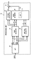
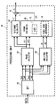
- the processing unit 38 includes a discrete Fourier transform circuit (DFT) 60, a phase calculator (calculator) 62, an amplitude calculator (calculator) 64, a distance calculator 66, an error estimator 68 and a corrector 70.
- the DFT 60 calculates, based on the data output from the A/D converter 36, real parts Re1, Re2 of the fundamental component and the second harmonic component and imaginary parts Im1, Im2 of the fundamental component and the second harmonic component.
- the DFT 60 outputs the real parts Re1, Re2 and the imaginary parts Im1, Im2 to the phase calculator 62 and the amplitude calculator 64.
- the phase calculator 62 calculates an estimation value (first phase angle ⁇ 1) of a phase difference of the fundamental component and an estimation value (second phase angle ⁇ 2) of a phase difference of the second harmonic component based on the real parts Re1, Re2 and the imaginary parts Im1, Im2 calculated by the DFT 60 with reference to the equation (2) as described above. Then, the phase calculator 62 outputs the first phase angle ⁇ 1 and the second phase angle ⁇ 2 to the distance calculator 66 and the error estimator 68.
- the amplitude calculator 64 calculates absolute values of amplitude A1, A2 of the fundamental component and the second harmonic component based on the real parts Re1, Re2 and the imaginary parts Im1, Im2 calculated by the DFT 60. Then, the amplitude calculator 64 outputs the amplitude A1, A2 to the error estimator 68.
- the amplitude for the fundamental component is referred to as "first amplitude A1” and the amplitude for the second harmonic component is referred to as "second amplitude A2".
- the distance calculator 66 obtains L' by, for example, linearly combining L1' and L2', i.e., a linear combination. It can be understood that, if the multipath occurs, the distance L' calculated by the distance calculator 66 includes an error value ⁇ L due to the multipath error. That is, the distance L' calculated by the distance calculator 66 may include the real distance value L and the error value ⁇ L.
- the error estimator 68 includes a lookup table (LUT) 72 therein and estimates, using the LUT 72, the error value ⁇ L based on the first phase angle ⁇ 1, the second phase angle ⁇ 2, the first amplitude A1 and the second amplitude A2. More specifically, the error estimator 68 estimates the error value ⁇ L based on (i) a phase difference between the first phase angle ⁇ 1 and a half value of the second phase angle ⁇ 2, i.e., ⁇ 1- ⁇ 2/2, and (ii) an amplitude ratio of the second amplitude A2 to the first amplitude A1, i.e., A1/A2, as will be described below.
- LUT lookup table
- Fig. 14 shows a mixed waveform of the reflected lightLL 1 through the direct path and the reflected light L 2 through the multi-reflected path (see Fig. 1(a)).
- the reflected light L 2 has phase delay of ⁇ due to the path length difference ⁇ d.
- the amplitude of the reflected light L 1 is A
- the amplitude of the reflected light L 2 can be represented as ⁇ A, where ⁇ is a reflection rate of the reflected light B through the multipath. Therefore, when multipath interference occurs, the mixed light L 1 +L 2 is generated by synthesizing the reflected light L 1 and the reflected light L 2 .
- Fig. 15 shows a relation between the error value ⁇ L due to the multipath error and the path length difference ⁇ d (Fig. 15(a)), a relation between the phase difference ⁇ 1- ⁇ 2/2 and the path length difference ⁇ d (Fig. 15(b)), and a relation between the amplitude ratio A2/A1 and the path length difference ⁇ d (Fig. 15(c)).
- the phase difference ⁇ 1- ⁇ 2/2 has a dependency on the path length difference ⁇ d.
- the amplitude ratio A2/A1 also has a dependency on the path length difference ⁇ d, as shown in Fig. 15 (c).
- the phase difference ⁇ 1- ⁇ 2/2 and the amplitude ratio A2/A1 can be used as reference information for the LUT 72 to calculate the error value ⁇ L that is also dependent on the path length difference ⁇ d.
- Fig. 16 shows the relation between the phase difference ⁇ 1- ⁇ 2/2 and the path length difference ⁇ d when the reflection rate ⁇ is 0.3, 0.5 or 0.7 (Fig. 16 (a)) and the relation between the amplitude ratio A2/A1 and the path length difference ⁇ d when the refection rate ⁇ is 0.3, 0.5 or 0.7 (Fig. 16 (b)).
- the relation between the phase difference ⁇ 1- ⁇ 2/2 and the path length difference ⁇ d varies according to the value of the reflection rate ⁇ .
- the relation between the amplitude ratio A2/A1 and the path length difference ⁇ d varies according to the value of the refection rate ⁇ .
- both the path length difference ⁇ d and the reflection rate ⁇ are calculated with two parameters ( ⁇ 1- ⁇ 2/2 and A2/A1) for the entire range of the path length difference ⁇ d to estimate the error value ⁇ L, its calculation would be complicated, resulting in increasing calculation load on the error estimator 68.
- the error estimator 68 uses approximation for a certain range to simplify the calculation for estimating the error value ⁇ L.
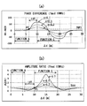
- Fig. 17 shows relations of the phase difference ⁇ 1- ⁇ 2/2 (Fig. 17 (a)) and the amplitude ratio A2/A1 (Fig. 17 (b)) relative to the error value ⁇ L in place of the path length difference ⁇ d.
- the phase difference ⁇ 1- ⁇ 2/2 is represented with the error value ⁇ L
- the phase difference ⁇ 1- ⁇ 2/2 can be approximated with a linear function C regardless of the value of the reflection rate ⁇ , as shown in Fig. 17 (a).
- the phase difference ⁇ 1- ⁇ 2/2 can be approximately represented with the error value ⁇ L using the linear function C.
- the amplitude ratio A2/A1 can be approximated for a certain range with a secondary function A regardless of the value of the reflection rate ⁇ , as shown in Fig. 17 (b).
- the amplitude ratio A2/A1 can be approximately represented using the error value ⁇ L with the secondary function A.
- a threshold ratio value THA1 (e.g., 0.7) of the amplitude ratio A2/A1 is set based on a crossing point P1 at which three graphs of the amplitude ratio A2/A1 for ⁇ of 0.3, 0.5 and 0.7 intersect, as shown in Fig. 16 (b).
- a threshold difference value THP1 (e.g., 8°) of the phase difference ⁇ 1- ⁇ 2/2 is set based on a crossing point P2 at which three graphs of the phase difference ⁇ 1- ⁇ 2/2 for ⁇ of 0.3, 0.5 and 0.7 intersect.
- the error value ⁇ L can be approximately calculated using the linear function C.
- the amplitude ratio A2/A1 is equal to or less than the THA1 and the phase difference ⁇ 1- ⁇ 2/2 is less than the THP1, the error value ⁇ L can be approximately calculated using the secondary function A.
- the LUT stores therein the linear function C and the secondary function A
- the error estimator 68 calculates the error value ⁇ L using only the amplitude ratio A2/A1 or the phase difference ⁇ 1- ⁇ 2/2 when the amplitude ratio A2/A1 and/or the phase difference ⁇ 1- ⁇ 2/2 are within the above described range.
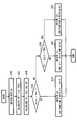
- Fig. 18 is a flowchart for a process performed by the processing unit 38 to estimate the error value ⁇ L.
- the processing unit 38 receives the electric charge data corresponding to the control signals D 1 to D 6 from the A/D converter 36, and the DFT 60 calculates, at Step 12, the real parts Re1, Re2 of the fundamental component and the second harmonic component and the imaginary parts Im1, Im2 of the fundamental component and the second harmonic component.
- the phase calculator 62 calculates the first phase angle ⁇ 1 and the second phase angle ⁇ 2, and the amplitude calculator 64 calculates the first amplitude A1 and the second amplitude A2.
- the error estimator 68 determines whether the amplitude ratio A2/A1 is greater than the threshold ratio value THA1. If the amplitude ratio A2/A1 is greater than the threshold ratio value THA1 (S16: YES), the error estimator 68 refers to the LUT 72 and estimates the error value ⁇ L using the linear function C stored in the LUT 72, at Step 18. Specifically, the error estimator 68 estimates the error value ⁇ L from the linear function C based on only the phase difference ⁇ 1- ⁇ 2/2 without considering the reflection rate ⁇ .
- the error estimator 68 determines whether the phase difference ⁇ 1- ⁇ 2/2 is less than the threshold difference value THP1 at Step 20. If the phase difference ⁇ 1- ⁇ 2/2 is less than the threshold difference value THP1 (S20: YES), the error estimator 68 refers to the LUT 72 and approximates the error value ⁇ L using the secondary function A stored in the LUT 72, at Step 22. More specifically, the error estimator 68 estimates the error value ⁇ L from the secondary function A based on only the amplitude ratio A2/A1 without considering the reflection rate ⁇ .
- the calculation can be simplified as compared to when the error value ⁇ L is calculated using two parameters ( ⁇ 1- ⁇ 2/2, A2/A1) in all cases, whereby processing load to the error estimator 68 can be reduced in the present embodiment.
- the calculation period can be reduced.
- the error estimator 68 When the error estimator 68 obtains the error value ⁇ L through the process showed in Fig. 18, the error estimator 68 outputs the error value ⁇ L to the corrector 70.
- the corrector 70 corrects L' obtained by the distance calculator 66 by subtracting the error value ⁇ L from the distance value L', whereby the corrector 70 obtains the corrected distance value L (i.e., a corrected distance to the object 12). Then, the corrector 70 (the processing unit 38) outputs the corrected distance value L.
- the receiver controller 30 generates the plurality of controls signals D N to simultaneously sense the fundamental component and the second harmonic component.
- the TOF device 20 and the method for detecting a multipath error according to the first embodiment may estimate the error value ⁇ L due to a multipath error with high accuracy.
- the third state (i.e., the null period) of the control signal D N is defined as a state where the first switch 48 and the second switch 50 are both on.
- the third state of the control signal D N is defined as a state where the first switch 48 and the second switch 50 are both off, as shown in Fig. 19.
- each pixel sensor 80 further includes a sub switch 74 that is electrically connected between the PD 42 and a discharge target (not shown).
- the sub switch 74 is controlled by a sub gate signal TG3 output from the receiver controller 30 such that the sub switch 74 is off during the first state (i.e., "1") and the second state (i.e., "-1") and is on during the third state (i.e., "0").
- electricity (Qc) generated during the third state is discharged through the sub switch 74 without being stored in the first capacitor 44 and the second capacitor 46.
- the electricity during the third state is not output from the pixel sensor 80, and thus data associated with the electricity generated during the third state is not used for calculating the error value ⁇ L.
- the data used to calculate the error value ⁇ L includes information of the second harmonic component as well as the fundamental component. In other words, the fundamental component and the second harmonic component can be simultaneously sensed, as with the first embodiment.
- the 6 different types of signals D 1 to D 6 are output to each sensing unit 40 to obtain data of 6 mutually phase-shifted electric charge output signals corresponding to the signals D 1 to D 6 .
- the emitted light includes the fundamental component and the second harmonic component, it is possible to sense the fundamental component and the second harmonic component with at least 5 different types of signals.
- the sensing unit 40 is formed of 5 pixel sensors A to E, and the receiver controller 30 generates 5 different types of signals D 1 to D 5 each having a different phase from each other. Then, the receiver controller 30 outputs, at the substantially same timing, the 5 different types of signals D 1 to D 5 to the 5 pixel sensors A to E. Thus, each pixel sensor A to E receives a respective one of the 5 different types of signals D 1 to D 5 .
- one pixel sensor 80 in one sensing unit 40 receives one type of signal.
- the pixel sensor A receives the signal D1 as shown in Fig. 12 in the first embodiment.
- the pixel sensor A may sequentially receive different types of signals D N .
- Fig. 21 shows a sampling time period necessary for obtaining data of 6 mutually phase-shifted electric charge output signals according to the fourth embodiment.
- the comparative example is the same as the comparative example shown in Fig. 12.
- the plurality of control signals D N includes 6 types of signals D 1 to D 6 each having a different phase from each other.
- the receiver controller 30 sequentially outputs the 6 different types of signals D 1 to D 6 to one pixel sensor A such that the pixel sensor A receives, in order, all of the 6 different types of signals D 1 to D 6 .
- the TOF device 20 further includes a frame memory 76 between the A/D converter 36 and the processing unit 38 as shown in Fig. 22.
- the frame memory 76 is a temporary storage to store the data sequentially generated from the signals D 1 to D 5 , and when the final data corresponding to the signal D 6 is obtained, the processing unit 38 calculates the distance value L' and the error value ⁇ L using the final data corresponding to the signal D 6 and the data of 5 electric charge output signals stored in the frame memory 76.
- the receiver controller 30 generates and outputs the signal D 1 to the pixel sensor A at a first specified timing, and then the data corresponding to the signal D 1 is outputted from the pixel sensor A. Then, the frame memory 76 temporally stores the data corresponding to the signal D 1 . In this case, the fundamental component and the second component are reflected in the data corresponding to the signal D 1 as indicated by f1/f2 in Fig. 21. Next, the receiver controller 30 generates and outputs the signal D 2 to the pixel sensor A at a second specified timing, and then the data corresponding to the signal D 2 is stored in the frame memory 76. Similarly, the fundamental component and the second component of the reflected light are reflected in the data corresponding to the signal D 2 .
- the receiver controller 30 repeatedly generates and outputs the signals D 1 to D 6 in the fourth embodiment, and all data reflecting the fundamental component and the second harmonic component corresponding to the signals D 1 to D 6 are obtained over six specified timings.
- the pixel sensor A according to the comparative example sequentially receives the signals D 1 to D 6 with the fundamental component first, and then receives the signals D 1 to D 6 with the second harmonic component. Therefore, the comparative example needs for two times the sampling time period of the fourth embodiment to obtain the data corresponding to the signals D 1 to D 6 with the fundament component and the second harmonic component.
- sampling time period for the fourth embodiment is longer than the first embodiment (refer to Fig. 12)
- one pixel sensor A detects the data corresponding to the signals D 1 to D 6 . Therefore, resolution of the light receiver 26 can be increased as compared to the first embodiment where the 6 data corresponding to the signals D 1 to D 6 are obtained by 6 pixel sensors A to F.
- Fig. 23 shows one sensing unit 40 of the light receiver 26 according to the fifth embodiment.
- each sensing unit 40 is formed of a subset of 3 pixel sensors (pixel sensor A to C).
- the plurality of control signals D N includes 6 different types of signals D 1 to D 6 and the 6 different types of signals D 1 to D 6 are further grouped into 2 subsets of 3 different types of signals. More specifically, one subset of 3 different types of signals is formed of signals D 1 to D 3 , and the other subset of 3 different types of signals is formed of signals D 4 to D 6 .
- the receiver controller 30 outputs, at each of 2 specified timings, a respective one of the 2 subsets of 6 different types of signals to the subset of 3 pixel sensors A to C such that each pixel sensor 80 of the subset of 3 pixel sensors A to C receives a different respective one of the outputted subset of 3 different types of signals. Accordingly, the subset of 3 pixel sensors A to C receives, over the 2 specified timings, all of the 6 types of signals D 1 to D 6 .
- the receiver controller 30 outputs, at a first specified timing, a respective one of the 2 subset of the signals D 1 to D 3 to the pixel sensors A to C.
- the pixel sensor A receives the signal D 1
- the pixel sensor B receives the signal D 2
- the pixel sensor C receives the signal D 3 .
- the data corresponding to the signal D 1 is obtained from the pixel sensor A
- the data corresponding to the signal D 2 is obtained from the pixel sensor B
- the data corresponding to the signal D 3 is obtained from the pixel sensor C
- each data reflects the fundamental component and the second harmonic component is temporally stored in a frame memory (not shown) that is the same as the frame memory 76 shown in Fig. 22.
- the receiver controller 30 outputs, at a second specified timing, a respective one of the other of the 2 subsets of signals D 4 to D 6 to the pixel sensors A to C.
- the pixel sensor A receives the signal D 4
- the pixel sensor B receives the signal D 5
- the pixel sensor C receives the signal D 6 .
- the data corresponding to the signal D 4 is obtained the pixel sensor A
- the data corresponding to the signal D 5 is obtained from the pixel sensor B
- the data corresponding to the signal D 6 is obtained from the pixel sensor C.
- 6 data corresponding to the signals D 1 to D 6 reflecting the fundamental component and the second harmonic component are obtained through the 2 specified timings, and then the processing unit 38 calculates the distance value L' and the error value ⁇ L using the 6 data.
- the sampling time period according to the fifth embodiment is shorter than the comparative example that is the same as the comparative example shown in Fig. 12.
- the TOF device 20 according to the fifth embodiment can detect the multipath error with a reduced time lag.
- the sampling time period (i.e., two specified timings) in the fifth embodiment is longer than the sampling period in the first embodiment (i.e., one specified timing) as shown in Fig. 12, since the data of 6 output signals corresponding to the signals D 1 to D 6 are obtained from the 3 pixel sensors A to C, resolution of the light receiver 26 can be increased compared to the first embodiment where the data of 6 output signals corresponding to the signals D 1 to D 6 are obtained by 6 pixel sensors A to F.
- the frame memory is necessary to store the data obtained during the first specified timing, the amount of data to be stored (i.e., data of 3 output siganls corresponding to the signals D 1 to D 3 ) is less than the fourth embodiment where data of 5 output signals corresponding to the signals D 1 to D 5 are stored in the frame memory. Therefore, the memory capacity of the frame memory in the fifth embodiment can be reduced as compared to the fourth embodiment.
- the sensing unit 40 is formed of the subset of 3 pixel sensors A to C and the receiver controller 30 outputs the signals D 1 to D 3 first, and then the signals D 4 to D 6 , to the 3 pixel sensors A to C.
- the number of the pixel sensors 80 forming the subset i.e., one sensing unit 40
- the control signals includes N different types of signals D 1 to D N , where N is greater than M
- the N different types of signals D 1 to D N may be grouped into K subsets of M different types of signals, where K is N/M.
- the receiver controller 30 may output, at each of K specified timings, a respective one of the K subsets of M different types of signals to the subset of M pixel sensors 80.
- the sensing unit 40 is formed of 2 pixel sensors A and B, and the control signals includes 6 different types of signals D 1 to D 6
- the 6 different types of signals D 1 to D 6 are grouped into 3 (i.e., 6/2) subsets of 2 different types of signals (e.g., D 1 -D 2 , D 3 -D 4 , and D 5 -D 6 ).
- the receiver controller 30 outputs, at a first specified timing, the signals D 1 and D 2 to the pixel sensors A and B, respectively, and then, at a second specified timing, the signals D 3 and D 4 to the pixel sensors A and B, respectively, and lastly, at a third specified timing, the signals D 5 and D 6 to the pixel sensors A and B, respectively.
- Fig. 25 shows the light receiver 26 according to the sixth embodiment.
- the sensing unit 40 is formed of a subset of 6 pixel sensors A to F and the control signals D N include 6 different types of signals D 1 to D 6 .
- the receiver controller 30 outputs, at each of 6 specified timings, the 6 different types of signals D 1 to D 6 to the subset of 6 pixel sensors A to F such that each pixel sensor 80 of the subset of 6 pixel sensors A to F receives a different respective one of the 6 different types of signals D 1 to D 6 .
- each pixel sensor 80 of the subset of 6 pixel sensors A to F receives, over the 6 specified timings, all of the 6 different types of signals D 1 to D 6 .
- the receiver controller 30 outputs the 6 signals D 1 to D 6 to the pixel sensors A to F, and therefore, the pixel sensor A receives the signal D 1 , the pixel sensor B receives the signal D 2 , the pixel sensor C receives the signal D 3 , the pixel sensor D receive the signal D 4 , the pixel sensor E receives the signal D 5 and the pixel sensor F receives the signal D 6 .
- the pixel sensor A receives the signal D 1
- the pixel sensor B receives the signal D 2
- the pixel sensor C receives the signal D 3
- the pixel sensor D receive the signal D 4
- the pixel sensor E receives the signal D 5
- the pixel sensor F receives the signal D 6 .
- the receiver controller 30 outputs the 6 signals D 1 to D 6 again to the pixel sensors A to F so that the pixel sensor A receives the signal D 2 , the pixel sensor B receives the signal D 4 , the pixel sensor C receives the signal D 1 , the pixel sensor D receives the signal D 6 , the pixel sensor E receives the signal D 3 , and the pixel sensor F receives the signal D 5 .
- the pixel sensor A receives the signals D 1 ⁇ D 2 ⁇ D 4 ⁇ D 6 ⁇ D 5 ⁇ D 3
- the pixel sensor B receives the signals D 2 ⁇ D 4 ⁇ D 6 ⁇ D 5 ⁇ D 3 ⁇ D 1
- the pixel sensor C receives the signals D 3 ⁇ D 1 ⁇ D 2 ⁇ D 4 ⁇ D 6 ⁇ D 5
- the pixel sensor D receives the signals D 4 ⁇ D 6 ⁇ D 5 ⁇ D 3 ⁇ D 1 ⁇ D 2
- the pixel sensor E receives the signals D 5 ⁇ D 3 ⁇ D 1 ⁇ D 2 ⁇ D 4 ⁇ D 6
- the pixel sensor F receives the signals D 6 ⁇ D 5 ⁇ D 3 ⁇ D 1 ⁇ D 2 ⁇ D 4 , in this order, through the 6 specified timings.
- data of 6 output signals corresponding to the signals D 1 to D 6 are obtained from the different pixel sensors A to F.
- each pixel sensor A to F receives all 6 different types of signals D 1 to D 6 through the 6 specified timings.
- the data of 6 output signals corresponding to the signals D 1 to D 6 can be obtained from each pixel sensors A to F. Accordingly, even if there is abnormality in one of pixel sensors A to F occurs (i.e., mismatch error occurs), since other pixel sensors A to F detect all types of data corresponding to the signals D 1 to D 6 , the mismatch error can be compensated (reduced).
- the control signals includes 6 different types of signals D 1 to D 6 and the sensing unit 40 is formed of the 6 pixel sensors A to F.
- the number of the types of the signals and the pixel sensors 80 forming the sensing unit 40 may be changed. That is, if the control signals includes N different types of signals D 1 to D N , and the sensing unit 40 is formed of a subset of N pixel sensors 80, the receiver controller 30 may output, at each of N specified timings, the N different types of signals D 1 to D 6 to the subset of N pixel sensors 80 such that each pixel sensor 80 of the subset of N pixel sensors 80 receives a different respective one of the N different types of signals D 1 to D 6 . As a result, each pixel sensor 80 of the subset of N pixel sensors 80 receives, over the N specified timings, all of the N different types of signals D 1 to D 6 .
- the receiver controller 30 outputs, at each of 5 specified timings, the 5 different types of signals D 1 to D 5 to the 5 pixel sensors A to E.
- each pixel sensor A to E receives, over the 5 specified timings, all of the 5 signals D 1 to D 5 .
- Fig. 26 shows the light receiver 26 according to the seventh embodiment.
- the sensing unit 40 is formed of a subset of 4 pixel sensors A to D and the control signals D N include 5 different types of signals D 1 to D 5 each having a different phase from each other.
- the receiver controller 30, at each of 5 specified timings, selects a subset of 4 types of signals from the 5 different types of signals D 1 to D 5 and outputs the selected subset of 4 types of signals to the subset of 4 pixel sensors A to D such that each of the subset of 4 pixel sensors A to D receives a different respective one of the selected subset of 4 signals.
- the subset of 4 different types of signals selected at each of the 5 specified timings includes at least one different types of signals as compared to the subset of 4 different types of signals selected at all other ones of the 5 specified timings.
- each pixel sensor 80 of the subset of 4 pixel sensors A to D receives, over the 5 specified timings, all of the 5 different types of signals D 1 to D 5 .
- the receiver controller 30 selects, at a first specified timing, the signals D 1 to D 4 as a first subset from the 5 different types of signals D 1 to D 5 , and then outputs the selected signals D 1 to D 4 to the pixel sensors A to D. Accordingly, during the first specified timing, the pixel sensor A receives the signal D 1 , the pixel sensor B receives the signal D 2 , the pixel sensor C receives the signal D 3 , and the pixel sensor D receives he signal D 4 .
- the receiver controller 30 selects, at a second specified timing, the signals D 5 , D 1 , D 2 and D 3 as a second subset from the 5 different types of signals D 1 to D 5 .
- the second subset of the D 5 , D 1 , D 2 and D 3 selected at the second specified timing includes the signal D 5 that is a different type of signal as compared to the first subset of the signals D 1 to D 4 selected at the first specified timing.
- the receiver controller 30 outputs the signals D 5 , D 1 , D 2 and D 3 to the pixel sensors A to D. Accordingly, during the second specified timing, the pixel sensor A receives the signal D 5 , the pixel sensor B receives the signal D 1 , the pixel sensor C receives the signal D 2 and the pixel sensor D receives the signal D 3 .
- the receiver controller 30 selects, at a third specified timing, the signals D 4 , D 5 , D 1 and D 2 as a third subset from the 5 different types of signals D 1 to D 5 .
- the third subset of the D 4 , D 5 , D 1 and D 2 selected at the third specified timing includes the signal D 4 that is a different type of signal as compared to the second subset of the signals D 5 , D 1 , D 2 and D 3 selected at the second specified timing.
- the third subset of the D 4 , D 5 , D 1 and D 2 selected at the third specified timing includes the signal D 5 that is a different type of signal as compared to the first subset of the signals D 1 to D 4 selected at the first specified timing.
- the receiver controller 30 outputs the signals D 4 , D 5 , D 1 and D 2 to the pixel sensors A to D.
- the pixel sensor A receives the signal D 4
- the pixel sensor B receives the signal D 5
- the pixel sensor C receives the signal D 1
- the pixel sensor D receives the signal D 2 .
- the pixel sensor A receives the signals D 1 ⁇ D 5 ⁇ D 4 ⁇ D 3 ⁇ D 2
- the pixel sensor B receives the signals D 2 ⁇ D 1 ⁇ D 5 ⁇ D 4 ⁇ D 3
- the pixel sensor C receives the signals D 3 ⁇ D 2 ⁇ D 1 ⁇ D 5 ⁇ D 4
- the pixel sensor E receives the signals D 4 ⁇ D 3 ⁇ D 2 ⁇ D 1 ⁇ D 5 , in this order, through the 5 specified timings.
- each of the pixel sensors A to D receives, over the 5 specified timings, all of the different types of 5 signals D 1 to D 5 .
- mismatch error occurs
- the seventh embodiment by switching the signals to be output to the pixel sensors A to D, 5 derived from to the 5 different signals D 1 to D 5 can be obtained by the 4 pixel sensors A to D.
- 5 derived from to the 5 different signals D 1 to D 5 can be obtained by the 4 pixel sensors A to D.
- the 5 different types of signals D 1 to D 5 are output to the 4 pixel sensors A to D.
- the number of the types of the signals and the pixel sensors 80 forming one sensing unit 40 may be changed. That is, if one sensing unit 40 is formed of a subset of M pixel sensors 80, the control signals include N different types of signals D 1 to D N , where N is greater than M.
- the receiver controller 30 selects a subset of M different types of signals form the N different types of signals D 1 to D N and outputs the selected subset of M different types of signals to the subset of M pixel sensors 80 such that each of the subset of M pixel sensors 80 receives a different respective one of the selected subset of M pixel sensors 80.
- the subset of M different types of signals selected at each of the N specified timings includes at least one different types of signals as compared to the subset of M different types of signals selected at all other ones of the N specified timings.
- each pixel sensor 80 of the subset M pixel sensors 80 receives, over the N specified timings, all of the N different types of signals D 1 to D N .
- the receiver controller 30 selects a subset of 4 different types of signals from the 6 different types of signals D 1 to D 6 and outputs the selected subset of 4 different types signals to the subset of 4 pixel sensors A to D.
- the receiver controller 30, at each of 6 specified timings selects a subset of 5 different types of signals from the 6 different types of signals D 1 to D 6 and outputs the selected subset of 5 different types of signals to the subset of 5 pixel sensors A to E.
- the error estimator 68 estimates the error value ⁇ L using the linear function C or the secondary function A (refer to Figs. 17 and 18).
- the error estimator 68 estimates the error value ⁇ L using other linear functions in addition to the linear function C and the secondary function A. More specifically, the LUT 72 stores two additional linear functions (a first sub linear function B1 and a second sub linear function B2) as defined in Figs. 27 and 28, which are the same types of graphs as those of Figs. 16 and 17 described in the first embodiment.
- phase difference ⁇ 1- ⁇ 2/2 when the phase difference ⁇ 1- ⁇ 2/2 is represented with the error value ⁇ L, the phase difference ⁇ 1- ⁇ 2/2 for the reflection rate ⁇ is 0.3 can be approximated with the sub linear function B1 in a certain range (between THP1 and THP2 as shown in Fig. 28). Furthermore, the phase difference ⁇ 1- ⁇ 2/2 for the reflection rate ⁇ is 0.5 can be approximated with the sub linear function B2 in a certain range (between THP2 and THP3 as shown in Fig. 28).
- the first threshold ratio value THA1 e.g., 0.7
- the threshold ratio value THA1 described in the first embodiment is the same as the threshold ratio value THA1 described in the first embodiment.
- the first threshold difference value THP1 e.g., 8°
- the threshold difference value THP1 described in the first embodiment is the same as the threshold difference value THP1 described in the first embodiment.
- the LTU stores therein the liner function C, the first sub linear function B1, the second sub linear function B2 and the secondary function A, and the error estimator 68 calculates the error value ⁇ L using only the amplitude ratio A2/A1 or the phase difference ⁇ 1- ⁇ 2/2 within a certain range defined by the first to third threshold ratio values THA1, THA2, THA3 and the first to third threshold difference values THP1, THP2, THP3.
- the error estimator 68 presumes, on condition that the amplitude ratio A2/A1 is below the THA2, the reflection rate ⁇ to be 0.3 and approximates the ⁇ L using the first sub linear function B1. Furthermore, when the phase difference ⁇ 1- ⁇ 2/2 is between the THP2 and the THP3, the error estimator 68 presumes, on condition that the amplitude ratio A2/A1 is below the THA3, the reflection rate ⁇ to be 0.5 and approximates the ⁇ L using the second sub linear function B2.
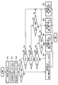
- Fig. 29 is a flowchart according to the eighth embodiment for a process performed by the processing unit 38 to estimate the error value ⁇ L. Since the processing at Steps 10 to 14 is similar to the processing shown in Fig. 18, the description of the processing at Steps 10 to 14 is omitted.
- the error estimator 68 determines whether the amplitude ratio A2/A1 is greater than the first threshold ratio value THA1. If the amplitude ratio A2/A1 is greater than the first threshold ratio value THA1 (S16: YES), the error estimator 68 refers to the LUT 72 and approximates the error value ⁇ L using the linear function C stored in the LUT 72 at Step 18. Specifically, the error estimator 68 estimates the error value ⁇ L from the linear function C with only the phase difference ⁇ 1- ⁇ 2/2 without considering the reflection rate ⁇ .
- the error estimator 68 determines whether the phase difference ⁇ 1- ⁇ 2/2 is less than the first threshold difference value THP1 at Step 20. If the phase difference ⁇ 1- ⁇ 2/2 is less than the first threshold difference value THP1 (S20: YES), the error estimator 68 refers to the LUT 72 and approximates the error value ⁇ L using the secondary function A stored in the LUT 72 at Step 22. More detail, the error estimator 68 estimates the error value ⁇ L from the secondary function A with only the amplitude ratio A2/A1 without considering the reflection rate ⁇ .
- the error estimator 68 determines whether the phase difference ⁇ 1- ⁇ 2/2 is less than the second threshold difference value THP2 at Step 30.
- the process proceeds to Step 32 where the error estimator 68 determines whether the amplitude ratio A2/A1 is greater than the second threshold ratio value THA2.
- Step 34 the error estimator 68 determines whether the phase difference ⁇ 1- ⁇ 2/2 is less than the third threshold difference value THP3.
- the error estimator 68 refers to the LUT 72 and approximates the error value ⁇ L using the secondary function A stored in the LUT 72 at Step 22.
- the error estimator 68 refers to the LUT 72 and approximates the error value ⁇ L using the first sub linear function B1 stored in the LUT 72 at Step 36. More specifically, the error estimator 68 estimates the error value ⁇ L from the first sub linear function B1 with only the phase difference ⁇ 1- ⁇ 2/2 by presuming the reflection rate ⁇ is 0.3.
- Step 34 when the phase difference ⁇ 1- ⁇ 2/2 is less than the third threshold difference value THP3 (S34: YES), the process proceeds to Step 38 where the error estimator 68 determines whether the amplitude ratio A2/A1 is greater than the third threshold ratio value THA3. On the other hand, when the phase difference ⁇ 1- ⁇ 2/2 is equal to or greater than the third threshold difference value THP3 (S34: NO), the error estimator 68 refers to the LUT 72 and approximates the error value ⁇ L using the linear function C stored in the LUT 72 at Step 18.
- the error estimator 68 refers to the LUT 72 and approximates the error value ⁇ L using the secondary function A stored in the LUT 72 at Step 22.
- the error estimator 68 refers to the LUT 72 and approximates the error value ⁇ L using the second sub linear function B2 stored in the LUT 72 at Step 40. More specifically, the error estimator 68 estimates the error value ⁇ L from the second sub linear function B2 with only the phase difference ⁇ 1- ⁇ 2/2 by presuming the reflection rate ⁇ is 0.5.
- the error estimator 68 estimates the error value ⁇ L using a single parameter in the above-described range defined by the first to third threshold difference values THA1, THA2, THA3 and the first to third threshold ratio values THP1, THP2, THP3.
- the calculation can be simplified compared to when the error value ⁇ L is calculated using two parameters ( ⁇ 1- ⁇ 2/2, A2/A1) considering the reflection rate ⁇ , whereby processing load to the error estimator 68 can be reduced.
- the TOF device 20 Refers to the ninth embodiment. If a foggy condition exists in the scene, the amplitude ratio A2/A1 tends to have a small value (e.g., 0.2). However, the amplitude ratio A2/A1 is also low when multipath interference exists. Therefore, when a small value of the amplitude ratio A2/A1 is calculated, the error estimator 68 may not be able to differentiate whether the small value of the amplitude ratio A2/A1 is due to the multipath interference or a foggy condition. Therefore, if a foggy condition exists, the error estimator 68 may falsely determine that the multipath interference occurs.
- a foggy condition exists in the scene, the amplitude ratio A2/A1 tends to have a small value (e.g., 0.2). However, the amplitude ratio A2/A1 is also low when multipath interference exists. Therefore, when a small value of the amplitude ratio A2/A1 is calculated, the error estimator 68 may not be able to differentiate whether the small value of
- the error estimator 68 further includes a foggy condition determiner 78 as shown in Fig. 30.
- a foggy condition exists, almost all of the pixel sensors 80 detect data affected by the foggy condition, and therefore almost all of the amplitude ratios A2/A2 obtained from the pixel sensors 80 tend to have a small value.
- the multipath occurs, only some pixel sensors 80 detect data affected by the multipath interference, whereby only some of the amplitude ratios A2/A1 have a small value.
- the foggy condition determiner 78 determines that the foggy condition exists when a predetermined ratio (e.g., 90%) of the pixel sensors 80 shows the amplitude ratio A2/A1 having a value less than a foggy condition threshold value (e.g., 0.2).
- a predetermined ratio e.g. 90%
- a foggy condition threshold value e.g., 0.2
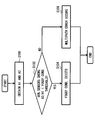
- Fig. 31 illustrates a flowchart of a process to determine the existence of a foggy condition.
- the foggy condition determiner 78 determines whether 90% of the pixel sensors 80 show the amplitude ratio A2/A1 having a value less than 0.2 (the foggy condition threshold value) at Step 102.
- the foggy condition determiner 78 determines that a foggy condition exists in the scene at Step 104.
- the foggy condition determiner 78 determines that a multipath error occurs at Step 106. In this way, the foggy condition determiner 78 can determine the existence of the foggy condition or the occurrence of the multipath error. Therefore, the TOF device 20 according to the ninth embodiment can obtain the distance value L with high accuracy.
- the emitted light is controlled to have a 25% duty ratio (i.e., less than 50%).
- the emitted light may be controlled to have a duty cycle more than 50%.
- the second-order harmonic component can be sensed by the light receiver 26 by introducing the third state in the control signals. Accordingly, even if there is a situation where it is difficult to set a duty cycle to be less than 50%, the second-order harmonic component can be detected.
Landscapes
- Engineering & Computer Science (AREA)
- Physics & Mathematics (AREA)
- Computer Networks & Wireless Communication (AREA)
- General Physics & Mathematics (AREA)
- Radar, Positioning & Navigation (AREA)
- Remote Sensing (AREA)
- Electromagnetism (AREA)
- Optical Radar Systems And Details Thereof (AREA)
Abstract
The present disclosure relates to a time-of-flight distance measuring device. The device includes a light source (24) that emits emitted light toward an object (12), a light receiver (26) that includes photodetectors (80). The light receiver (26) detects reflected light reflected by the object. A first controller (28) controls the light source to emit the emitted light such that the emitted light includes a fundamental component and at least one harmonic component. A second controller (30) generates control signals (DN) and outputs each of the control signals to a respective photodetectors. A calculator (62, 64) calculates amplitudes (A1, A2) and phase angles (θ1, θ2). An error estimator (68) estimates an error value (ΔL) of a multipath error. The second controller generates the plurality of control signals to simultaneously sense the fundamental component and the at least one harmonic component.
Description
The present disclosure relates to a time-of-flight distance measuring device and a method for detecting a multipath error.
As a method for measuring the distance to an object in a scene, a time-of-flight (TOF) technology has been developed. Such a TOF technology may be used in a variety of fields, such as automotive industries, human-interfaces and gaming, robotics or the like. Generally, the TOF technology works by illuminating a scene with modulated light emitted from a light source and by observing reflected light reflected by an object in the scene. By measuring the phase difference between the emitted light and the reflected light, the distance to the object is calculated (see, e.g., Patent Literatures 1 to 4).
In a distance measuring device using such a conventional TOF technology, multipath interference may affect the accuracy of the measured distance. The multipath interference arises when the emitted light travels along multiple paths that have a different path length from each other and then is sensed by a single photo receiver as integrated light. Although the phases of light along the different path lengths are different each other, the conventional distance measuring device computes a distance based on mixed phases of the integrated light. Therefore, the computed distance may include an error value arising from the multipath interference.
To mitigate the error associated with the multipath interference, methods of using a plurality of sequential measurements with different modulation frequencies are known (refer to, e.g., Patent Literatures 5 to 7). However, these methods require sequentially calculating distances using different modulation frequencies, which may generate a time lag to detect a multipath error.
This section provides a general summary of the disclosure, and is not a comprehensive disclosure of its full scope or all of its features.
The objective of the present disclosure is to provide a time-of-flight distance measuring device and a method for detecting a multipath error that may estimate an error value associated with a multipath error without a time lag or with a reduced time lag.
In a first aspect of the present disclosure, a time-of-flight distance measuring device includes (i) a light source that emits light, as emitted light, toward an object, (ii) a light receiver that includes a plurality of photodetectors, the light receiver detecting, as reflected light, the emitted light reflected by the object, (iii) a first controller that controls the light source to emit the emitted light as an amplitude-modulated waveform such that the emitted light includes a fundamental component at a fundamental frequency and at least one harmonic component of the fundamental frequency, (iv) a second controller that generates a plurality of control signals and outputs each of the plurality of control signals to a respective one of the plurality of photodetectors, (v) a calculator that calculates amplitudes and phase angles of the fundamental component and the at least one harmonic component based on a detection value of the light receiver, and (vi) an error estimator that estimates an error value associated with a multipath error based on the amplitudes and the phase angles calculated by the calculator. The second controller generates the plurality of control signals to simultaneously sense the fundamental component and the at least one harmonic component of the reflected light.
According to the first aspect of the present disclosure, the second controller generates the plurality of controls signals to simultaneously sense the fundamental component and the at least one harmonic component. Thus, it is possible to avoid generating a time lag or to reduce a time lag when obtaining data of the reflected light. Therefore, the time-of-flight distance measuring device according to the first aspect may estimate an error value due to a multipath error with high accuracy.
In a second aspect of the present disclosure, a method for detecting a multipath error using a time-of-flight distance measuring technology includes (i) emitting light, as emitted light, from a light source toward an object, (ii) detecting, as detected light, the emitted light reflected by the object by a light receiver, the light receiver including a plurality of photodetectors, (iii) controlling the light source to emit the emitted light as an amplitude-modulated waveform such that the emitted light includes a fundamental component at a fundamental frequency and at least one harmonic component of the fundamental frequency, (iv) generating a plurality of control signals and outputting each of the plurality of control signals to a respective one of the plurality of photodetectors, (v) calculating amplitudes and phase angles of the fundamental component and the at least one harmonic component based on a detection value of the light receiver, and (vi) estimating an error value associated with a multipath error based on the amplitudes and the phase angles calculated by the calculator. The plurality of control signals are generated to simultaneously sense the fundamental component and the at least one harmonic component of the reflected light.
According to the second aspect of the present disclosure, the plurality of controls signals is generated to simultaneously sense the fundamental component and the at least one harmonic component. Thus, it is possible to avoid generating a time lag or to reduce a time lag when obtaining data of the reflected light. Therefore, the method for detecting a multipath error may estimate an error value due to a multipath error with high accuracy.
Further areas of applicability will become apparent from the description provided herein. The description and specific examples in this summary are intended for purposes of illustration only and are not intended to limit the scope of the present disclosure.
The disclosure, together with additional objectives, features and advantages thereof, will be best understood from the following description, the appended claims and the accompanying drawings, in which:
Figure 1 is an explanatory model where multipath interference occurs (Fig. 1(a)) and the multipath interference is resolved (Fig. 1(b)).
Figure 2 is a schematic view of a time-of-flight distance measuring device according to a first embodiment.
Figure 3 is a plan view of pixel sensors according to the first embodiment.
Figure 4 is a schematic view of the pixel sensor according to the first embodiment.
Figure 5 is one example of a signal sequence for one pixel sensor.
Figure 6 is one example of a differential signal sequence for one pixel sensor.
Figure 7 is emitted light at a 25% duty cycle according to the first embodiment.
Figure 8 is a graph showing a relation between amplitude and a duty cycle for a fundamental component, a second harmonic component and a third harmonic component.
Figure 9 is one example of a control signal according to the first embodiment.
Figure 10 is a schematic view of one pixel sensor when the pixel sensor is in a third state.
Figure 11 is the differential sequence of the control signals according to the first embodiment.
Figure 12 is a comparative view of a sampling sequence according to the first embodiment and a comparative example.
Figure 13 is a schematic view of a processing unit according to the first embodiment.
Figure 14 is a schematic view illustrating a mechanism of generating mixed light.
Figure 15 is a graph showing a relation between a multipath error and a path length difference (Fig. 15(a)), a relation between a phase difference and the path length difference (Fig. 15(b)), and a relation between an amplitude ratio and the path length difference (Fig. 15(c)).
Figure 16 is a graph showing the relation between the phase difference and the path length difference at a reflection rate of 0.3, 0.5 and 0.7 (Fig. 16(a)) and the relation between the amplitude ratio and the path length difference at the reflection rate of 0.3, 0.5 and 0.7 (Fig. 16(b)).
Figure 17 is a graph showing a relation between the phase difference and an error value at the reflection rate of 0.3, 0.5 and 0.7 (Fig. 17(a)) and a relation between the amplitude ratio and the error value at the reflection rate of 0.3, 0.5 and 0.7 (Fig. 17(b)).
Figure 18 is a flowchart showing a process to estimate the error value according to the first embodiment.
Figure 19 is a schematic view of one pixel sensor when the pixel sensor is in the third state according to a second embodiment.
Figure 20 is a schematic view of the pixel sensors according to a third embodiment.
Figure 21 is a comparative view of the sampling sequence according to a fourth embodiment and a comparative example.
Figure 22 is a schematic view of the processing unit according to the fourth embodiment.
Figure 23 is a schematic view of the pixel sensors according to a fifth embodiment.
Figure 24 is a comparative view of the sampling sequence according to the fifth embodiment and a comparative example.
Figure 25 is a schematic view of the pixel sensors according to a sixth embodiment.
Figure 26 is a schematic view of the pixel sensors according to a seventh embodiment.
Figure 27 is a graph showing the relation between the phase difference and the path length difference at a reflection rate of 0.3, 0.5 and 0.7 (Fig. 27(a)) and the relation between the amplitude ratio and the path length difference at the reflection rate of 0.3, 0.5 and 0.7 (Fig. 27(b)).
Figure 28 is a graph showing the relation between the phase difference and the error value at the reflection rate of 0.3, 0.5 and 0.7 (Fig. 28(a)) and the relation between the amplitude ratio and the error value at the reflection rate of 0.3, 0.5 and 0.7 (Fig. 28(b)).
Figure 29 is a flowchart showing a process to estimate the error value according to the eighth embodiment.
Figure 30 is a schematic view of the processing unit according to a ninth embodiment.
Figure 31 is a flowchart showing a process to determine a foggy condition according to the ninth embodiment.
A plurality of embodiments of the present disclosure will be described hereinafter referring to drawings. In the embodiments, a part that corresponds to a matter described in a preceding embodiment may be assigned with the same reference numeral, and redundant explanation for the part may be omitted. When only a part of a configuration is described in an embodiment, another preceding embodiment may be applied to the other parts of the configuration. The parts may be combined even if it is not explicitly described that the parts can be combined. The embodiments may be partially combined even if it is not explicitly described that the embodiments can be combined, provided there is no harm in the combination.
First, in order to facilitate technical understanding of the present disclosure, the fundamentals of multipath errors as related to each embodiment of the present disclosure will be explained with reference to Fig. 1.
Fig. 1(a) shows an explanatory model where multipath interference arises. In the model, a distance measuring device 10, as a comparative example to the present disclosure, is used to calculate a distance to an object (e.g., a pedestrian) 12 in a scene. The distance measuring device (hereinafter "comparative device") 10 emits light from a light source 14 and receives the light reflected by the object with a light receiver 16. In Fig. 1(a), a first path indicated by the solid line shows a direct path where the light emitted from the light source 14 directly reaches, and is reflected by, the object 12 and returns to the light receiver 16. On the other hand, a second path indicated broken line shows a multi-reflected path where the light emitted from the light source 14 is reflected first by an intermediate object, such as a vehicle, 18 and then the light is reflected by the object 12.
Where an actual path length along the direct path is d and an actual path length along the multi-reflected path is longer than the direct path by a path length difference Δd, the path length along the multi-reflected path can be represented as d+Δd. When the multipath interference arises, the comparative device 10 calculates a distance value L+ΔL, where L is a distance value arising from d and an error value ΔL arising from Δd. If the multipath error does not occur, the distance value L is nearly equal to the actual path length d.
In this model, for detecting the multipath error, the comparative device 10 sequentially emits the light with different frequencies. For example, the light source 14 emits the light with a first frequency f1 (e.g., 10MHz) for a predetermined period (e.g., 10msec) at a first timing, and then the light source 14 emits the light with a second frequency f2 (e.g., 20MHz) for the same period at a second timing. Therefore, it takes, in total, at least two predetermined periods (i.e., 20msec) for the comparative device 10 to detect the multipath error. In other words, a time lag due to the sequential emission of light is inevitably generated in the comparative example 10.
Because of the time lag, the distance value calculated by the comparative device 10 may still include an error in a situation described below. As shown in Fig. 1(a), a multipath arises during the measurement with the first frequency f1, but the multipath error is resolved when the intermediate object 18 moves away from the scene during the measurement with the second frequency f2 as shown in Fig. 1(b). In such a situation, the comparative device 10 obtains information affected by the multipath interference for the light with the first frequency f1, and then obtains information without the multipath interference for the light with the second frequency f2. Therefore, the comparative device calculates the error value using both the information affected by the multipath interference and the information not affected by the multipath interference. As a result, the error value of the multipath error calculated by the comparative device 10 may still be inaccurate.
In view of the above-described concern, the inventors of the present disclosure here present a plurality of embodiments of the time-of-flight distance measuring device that may detect a multipath error without a time lag or with a reduced time lag.
(First Embodiment)
Here, a time-of-flight distance measuring device and a method for detecting a multipath error according to the first embodiment will be described with reference to the accompanying drawings. In this embodiment, and other subsequent embodiments, the time-of-flight distance measuring device (hereinafter, collectively "TOF device") is used in a vehicle to calculate a distance to an object from the vehicle (i.e., the TOF device), but the usage of the TOF device is not limited to a vehicle. For example, the TOF device may be used for human-interface devices, gaming consoles, robots or the like. The "object" for the TOF device may include a pedestrian, other vehicles, obstacles on a road, buildings or the like.
Here, a time-of-flight distance measuring device and a method for detecting a multipath error according to the first embodiment will be described with reference to the accompanying drawings. In this embodiment, and other subsequent embodiments, the time-of-flight distance measuring device (hereinafter, collectively "TOF device") is used in a vehicle to calculate a distance to an object from the vehicle (i.e., the TOF device), but the usage of the TOF device is not limited to a vehicle. For example, the TOF device may be used for human-interface devices, gaming consoles, robots or the like. The "object" for the TOF device may include a pedestrian, other vehicles, obstacles on a road, buildings or the like.
(General Configuration)
Fig. 2 is a block diagram illustrating a general configuration of theTOF device 20 according to the first embodiment. The TOF device 20 includes a clock generator 22, a light source 24, a light receiver 26, an emitter controller (first controller) 28, a receiver controller (second controller) 30, a common-mode choke 32, a differential amplifier 34, an A/D converter 36 and a processing unit 38. The clock generator 22 generates and outputs a clock signal to both the emitter controller 28 and the receiver controller 30 to establish synchronization between the light source 24 and the light receiver 26. On receiving the clock signal from the clock generator 22, the emitter controller 28 and the receiver controller 30 generate and output a variety of signals to the light source 24 and the light receiver 26, respectively, to work in synchronism with each other.
Fig. 2 is a block diagram illustrating a general configuration of the
When the emitter controller 28 receives the clock signal from the clock generator 22, the emitter controller 28 outputs a square wave as an emission control signal to the light source 24. In this embodiment, the light source 24 emits light, as emitted light, with a square waveform (i.e., an amplitude-modulated waveform) corresponding to the emission control signal. Hence, the emitted light has a same waveform as the emission control signal. However, the light source 24 may emit light having a sine waveform, a triangle waveform, or a waveform with a pseudo random pattern.
The light source 24 is a light emitting diode (LED) that emits infrared light toward the object 12. Alternatively, a laser diode (LD) that emits infrared light may be used as the light source 24. The emitter controller 28 controls the light source 24 such that the emitted light includes a fundamental component at a fundamental frequency and at least one harmonic component of the fundamental frequency. In this embodiment, the emitted light includes the fundamental component (i.e., first-order component) at the fundamental frequency (e.g., 10MHz) and a second harmonic component (i.e., second-order component) at two times the fundamental frequency (e.g., 20MHz). The emitted light with the fundamental component and the second harmonic component is emitted from the single light source 24. The emitted light may include the fundamental component and two other harmonic components, such as the second and third harmonic components. Alternatively, the emitted light may include the fundamental component and another harmonic component other than the second harmonic component, such as the third harmonic, the fourth harmonic, or the like.
The receiver controller 30 generates and outputs a plurality of control signals (e.g., see D1 to D6 in Fig. 11) to the light receiver 26 to control a light receiving pattern of the light receiver 26. The receiver controller 30 generates the control signals DN such that the light receiver 26 simultaneously senses the fundamental component and the second harmonic component of the emitted light reflected by the object 12, as will be described later.
The light receiver 26 detects, as reflected light, the emitted light reflected by the object 12 in the scene. As shown in Fig. 3, the light receiver 26 includes a plurality of pixel sensors (photodetectors) 80 that are arranged in a regular array form. In the present embodiment, the plurality of pixel sensors 80 are grouped into a plurality of sensing units 40 and each sensing unit 40 is formed of six pixel sensors (subset of M photodetectors) 80. Hereinafter, the pixel sensors 80 forming one sensing unit 40 may be also referred to as the pixel sensors A to F in place of the reference numeral "80". The receiver controller 30 controls each sensing unit 40 as a single unit. The receiver controller 30 outputs each of the plurality of control signals DN to a respective one of the plurality of pixel sensors A to F through wiring CTL1 to CTL6. As will be described below, each control signal DN is a differential signal including a pair of normally complimentary gate signals TG1, TG2.
The pixel sensor 80 is an image sensor using CMOS (Complementary Metal Oxide Semiconductor) technology, CCD (Charge Coupled Device) technology, or combination of both the technologies. As shown in Fig. 4, each pixel sensor 80 includes a PD (photo diode, photo element) 42, a first capacitor 44, a second capacitor 46, a first switch 48 and a second switch 50. The first switch 48 and the second switch 50 are a MOS-type device, such as a MOS transistor or a transfer gate, or a charge-coupled device (CCD). The first capacitor 44 and the second capacitor 46 are a capacitive element, such as MOS, CCD or MIM (Metal Insulator Metal). The first capacitor 44 is electrically connected to the first switch 48, and the first switch 48 is electrically connected to the PD 42, and therefore the first capacitor 44 is electrically connected to the PD 42 through the first switch 48. Similarly, the second capacitor 46 is electrically connected to the second switch 50 and the second switch 50 is electrically connected to the PD 42, and therefore the second capacitor 46 is electrically connected to the PD 42 through the second switch 50.
The PD 42 generates electricity while being exposed to the reflected light. The control signal DN received from the receiver controller 30 operates the pixel sensor 80 by controlling an on/off state of the first switch 48 and the second switch 50. As mentioned before, the control signal DN includes a pair of gate signals TG1, TG2 that are normally complimentary For example, when the first switch 48 is on and the second switch 50 is off, the first capacitor 44 stores electric charge generated from the PD 42. On the other hand, when the first switch 48 is off and the second switch 50 is on, the second capacitor 46 stores electric charge generated from the PD 42. Although two pairs of a switch and a capacitor (i.e., the first switch 48 and the first capacitor 44, and the second switch 50 and the second capacitor 46) are used in the present embodiment, three or more pairs of a switch and a capacitor may be used. The electric charge stored in the first capacitor 44 and the electric charge stored in the second capacitor 46 are separately output to the common-mode choke 32 as analog data.
The common-mode choke 32 is used to avoid light saturation by removing common mode (CM) components from the data output from the pixel sensor 80. The CM components are generated when light saturation occurs, i.e., when sufficiently high background light exists in the scene. After removing the CM component, the data corresponding to the first capacitor 44 and the data corresponding to the second capacitor 46 are input into the differential amplifier 34. The differential amplifier 34 outputs the difference value between each pair of the electric charge data to the A/D converter 36. That is, the difference value between the data corresponding to the electric charge stored in the first capacitor 44 and the data corresponding to the electric charge stored in the second capacitor 46 are output from the differential amplifier 34.
The A/D converter 36 converts the analog data from the differential amplifier 34 to digital data and outputs the digital data to the processing unit 38. The processing unit 38 includes a CPU, a ROM, a RAM or the like, and performs programs stored in the ROM to execute a variety of processing. Especially, the processing unit 38 calculates the distance (a distance value L) to the object 12 based on the digital data output from the A/D converter 36. Further, the processing unit 38 estimates an error value ΔL due to a multipath error and corrects the distance based on the estimated error value ΔL.
(Simultaneous Sensing of 1st and 2nd Order Components)
Next, the distance calculation mechanism of TOF technology will be explained in detail. For ease of understanding, an explanation will be first given with reference to a basic TOF distance sensor implementation.
Next, the distance calculation mechanism of TOF technology will be explained in detail. For ease of understanding, an explanation will be first given with reference to a basic TOF distance sensor implementation.
(General Principle of TOF Measuring)
Fig. 5 shows one example of a signal sequence (modulation cycle: Tm, exposure period: Tw) where the emitted light has a 50% duty cycle and thepixel sensor 80 is controlled through the gate signalsTG1, TG2 having a different phase from each other. As shown in Fig. 5, the pixel sensor 80 is first controlled through a first pair of gate signals TG1-1, TG2-1, and then is controlled through a second pair of gate signals TG1-2, TG2-2. In other words, four samplings are executed in this model. The waveform (emitted light waveform 52) of the emitted light from the light source 24 is a square form in synchronism with the gate signals TG1, TG2.
Fig. 5 shows one example of a signal sequence (modulation cycle: Tm, exposure period: Tw) where the emitted light has a 50% duty cycle and the
The waveform (reflected light waveform 54) of the reflected light has a time difference relative to the emitted light waveform 52, and thus the reflected light waveform 54 is sensed as a waveform having a phase delay with a phase difference φ relative to the emitted light waveform 52. The first pair of gate signals TG1-1, TG2-1 has a phase difference of 180° from each other, and the second pair of gate signals TG1-2, TG2-2 has a phase difference of 180° from each other. Further, the first pair of gate signals TG1-1, TG2-1 and the second pair of gate signals TG1-2, TG2-2 have a phase difference of 90° from each other.
In this example, each gate signal TG1-1, TG2-1, TG1-2, TG2-2 is output for several to hundreds of thousands of cycles. The electric charges generated by the first pair of gate signals TG1-1, TG2-1 are obtained as data Q1, Q2, while the electric charges generated by the second pair gate signals TG1-2, TG2-2 are obtained as data Q3, Q4. Specifically, the data is a voltage value that is a converted value of the electric charge through electric charge voltage conversion. Then, the estimation value θ of the phase difference φ can be calculated by equation (1) using the discrete Fourier transform (DFT) with the data Q1 to Q4 obtained through the four samplings.
θ=tan-1((Q1-Q3)/(Q2-Q4)) (1)
θ=tan-1((Q1-Q3)/(Q2-Q4)) (1)
Although, the equation (1) represents an equation when four samplings are executed, the equation (1) can be generalized as to N phases (i.e., N samplings) as represented in equation (2).
θ=tan-1((ΣQk*sin(2π/N*k)/(ΣQk*cos(2π/N*k))) (2)
Thereafter, a distance to theobject 12 can be calculated based on a relationship between θ and the speed of light. It should be noted although these equations can be generally used to a distance to the object 12, the distance to the object 12 is calculated by using the phase angle of the fundamental component and the second harmonic component at the processing unit 38 in the first embodiment, as will be described below.
θ=tan-1((ΣQk*sin(2π/N*k)/(ΣQk*cos(2π/N*k))) (2)
Thereafter, a distance to the
(Differential Signal Sequence)
The first pair of gate signals TG1-1, TG2-1 and the second pair of gate signals TG1-2, TG2-2 can be represented by respective differential signals D1, D2, as shown in Fig. 6. It should be noted that the differential signal D1, D2 is an imaginary signal that indicates the state of the pair of gate signals TG1, TG2. As mentioned previously, the gate signals TG1, TG2 are normally complimentary. Thus in Fig. 6, the differential signal D1, D2 has a value of "1" when a first gate signal TG1 is "H" and a second gate signal TG2 is "L". In other words, when the differential signal D1, D2 has the value "1", the on/off state of thefirst switch 48 and the second switch 50 is a first state where the first switch 48 is on and the second switch 50 is off.
The first pair of gate signals TG1-1, TG2-1 and the second pair of gate signals TG1-2, TG2-2 can be represented by respective differential signals D1, D2, as shown in Fig. 6. It should be noted that the differential signal D1, D2 is an imaginary signal that indicates the state of the pair of gate signals TG1, TG2. As mentioned previously, the gate signals TG1, TG2 are normally complimentary. Thus in Fig. 6, the differential signal D1, D2 has a value of "1" when a first gate signal TG1 is "H" and a second gate signal TG2 is "L". In other words, when the differential signal D1, D2 has the value "1", the on/off state of the
In contrast, the differential signal D1, D2 has the value of "-1" when the first gate signal is "L" and the second gate signal is "H". In other words, when the differential signal D1, D2 has the value "-1", the on/off state of the first switch 48 and the second switch 50 is a second state where the first switch 48 is off and the second switch 50 is on. Therefore, the state of the pair of gate signals TG1, TG2 (i.e., the on/off state of the first and second switches 48, 50) can be represented by a differential signal (control signal DN) that is normally either "1" or "-1".
(Emitted Light in Present Embodiment)
As explained previously, in the first embodiment, the emitted light is emitted with a fundamental component and its second order harmonic component, which are reflected and then simultaneously sensed by thelight receiver 26. In order to simultaneously sense the reflected light at both the fundamental frequency and the second order harmonic, in the present embodiment: (i) the emitted light is emitted with a fundamental component and its second order harmonic at a duty cycle of less than 50% and (ii) the control signal is generated to be sensitive to the second harmonic component as well as the fundamental component.
As explained previously, in the first embodiment, the emitted light is emitted with a fundamental component and its second order harmonic component, which are reflected and then simultaneously sensed by the
In other words, although the emitted light described in the basic implementation of Fig. 5 has a 50% duty cycle, the emitter controller 28 in the present embodiment controls the light source 24 to emit the emitted light having a duty cycle of less than 50%. For example, the emitted light may be emitted with a duty cycle of 25%. By setting the emitted light to have a 25% duty cycle, the second harmonic component can be effectively sensed as described below. Fig. 7 shows the emitted light 56 having a 25% duty cycle in the present embodiment indicated by the solid line and a comparative emitted light 58 having a 50% duty cycle indicated by the broken line.
Fig. 8 shows a relation between amplitude and a duty cycle [%] for the fundamental component, the second harmonic component and the third harmonic component. As shown in Fig. 8, the amplitude of the second harmonic component and the third harmonic component gradually increase as the duty cycle decreases from 50%. Especially, the amplitude of the second harmonic component has a maximum value at a duty cycle of 25%. Therefore, by setting the emitted light to have a 25% duty cycle in the present embodiment, the amplitude of the second harmonic component can be sensitively detected. However, it should be understood that the duty cycle is not limited to 25%. As shown in Fig. 8, the amplitude of the second component and the third component are positive at duty cycles other than 25%. For example, if the emitted light includes the third harmonic component, the duty cycle may be set to, e.g., about 18% at which the third harmonic component has a maximum value.
(Control Signal in Present Embodiment)
In the present embodiment, thereceiver controller 30 generates each of the plurality of control signals DN to respective ones of the plurality of pixel sensors 80. Although the control signals DN are described as differential signals of the gate signals TG1, TG2 for the first switch 48 and the second switch 50 in the subsequent description, the differential signal is a representative signal that is physically implemented as a pair of normally complementary gate signals TG1, TG2 as explained previously.. As with the description in Fig. 6, the control signal DN as shown in Fig. 9 in the present embodiment switches the on/off state of the first and the second switches 48, 50 between the first state indicated by "1" and the second state indicated by "-1".
In the present embodiment, the
Furthermore, to simultaneously sense the fundamental component and the second harmonic component of the reflected light, the receiver controller 30 generates the control signal DN to have a value of “0”, which represents a null period, as shown in Fig. 9. As described below, the data of the electric charge during the null period is cancelled. As a result, the electricity generated from the PD 42 during the null period is not used for calculating the distance value L or the error value ΔL at the subsequent process.
In the present embodiment, the control signal DN has a value of “0” (i.e., the null period) when the first and second gate signals TG1, TG2, which are normally complimentary, are both set to be “H”. In other words, when the control signal DN has the value "0", the on/off state of the first switch 48 and the second switch 50 is a third state where the first switch 48 is on and the second switch 50 is on Furthermore, the control signal DN is generated such that the third state occurs between the first state and the second state.
As shown in Fig. 10, during the third state, the electricity generated from the PD 42 is evenly distributed to the first capacitor 44 and the second capacitor 46, and thus the first capacitor 44 stores the electric charge Qa and the second capacitor 46 stores the electric charge Qb that is equal to Qa during the third state (i.e., the null period). Therefore, the electric charges Qa and Qb stored during the third state are cancelled through the common-mode choke 32 and the differential amplifier 34, whereby the electric charges Qa and Qb are not used for calculating the distance value L and the error value ΔL at the processing unit 38. By cancelling the electric charges Qa and Qb, the data output from the differential amplifier 34 can include information associated with the second component as well as the fundamental component. In other words, the data associated with the fundamental component and the second component can be simultaneously obtained.
More specifically, to sense the second harmonic component, the third state (the discharging state) is inserted from 1/2π to 3/2π phase (i.e., 90° to 270°) in one cycle of the control signal DN as shown in Fig. 9. In other words, one cycle of the control signal DN is formed of the first state ("1") from 0 to 1/2π phase, the third state ("0") from 1/2π to 3/2π phase, and the second state ("-1") from 3/2π to 2π phase.
Fig. 11 shows a differential signal sequence for one sensing unit 40 with 6 pixel sensors A to F in the present embodiment. As shown in Fig. 11, the control signals are formed of 6 different types of signals D1 to D6 having a different phase from each other. More specifically, the signals D1 to D6 have a phase difference of, for example, 60° from each other. The receiver controller 30 outputs, at substantially the same time (specified timing), the 6 different types of signals D1 to D6 to the 6 pixel sensors A to F. The signals D1 to D6 are output for several hundreds to thousands of cycles. Each pixel sensor A to F receives a respective one of the 6 different signals D1 to D6. In other words, each pixel sensor A to F in one sensing unit 40 is controlled by a different phase, and thus outputs electric charge data having a different value. It should be noted that the receiver controller 30 outputs the same subset of the 6 different types of signals D1 to D6 to each sensing unit 40. Hence, each sensing unit 40 is controlled to sense the reflected light with the same light sensing pattern as another sensing unit 40.
As described above, the emitted light includes the fundamental component and the second harmonic component and has a 25% duty cycle. Further, the control signals are generated such that the light receiver 26 simultaneously senses the fundamental component and the second harmonic component. Thus, the data associated with the fundamental component and the second harmonic component can be obtained at substantially the same time. In other words, a sampling time period necessary for obtaining the data associated with the fundamental component and the second harmonic component can be shortened.
Here, Fig. 12 shows the sampling time period for obtaining the data of the fundamental component and the second harmonic component according to the present embodiment and a comparative example. In the comparative example, the light source is controlled to emit the emitted light with the fundamental component indicated by "f1" in Fig. 12 (and light receiver is controlled to receive the reflected light) at a first timing, and then emit the emitted light with the second harmonic component indicated by "f2" in Fig. 12 (and receive the reflected light) at a second timing. Furthermore, the 6 different signals D1 to D6 are sequentially (i.e., not simultaneously) output to one pixel sensor A for the first timing to sense the fundamental component. The data corresponding to the 6 different signals D1 to D6 is temporally stored in a frame memory (not shown).
Then, the 6 different signals D1 to D6 are sequentially output again to the one pixel sensor A at the second timing to sense the second harmonic component. Thereafter, the data obtained at the second timing and the data stored in the frame memory are used to calculate a distance and an error value due to a multipath error.
As described above, the fundamental component and the second harmonic component (indicated by "f1/f2") are sensed at substantially the same time in the present embodiment as shown in Fig. 12. In contrast, in the comparative example, the signals D1 to D6 are output in turn and twelve signals D1 to D6 are sequentially output in total. Therefore, the sampling time period in the present embodiment is shorter than the comparative example. More specifically, the sampling time period for the present embodiment is about 1/12 of the comparative example.
Therefore, since the data of the fundamental component and the second harmonic component can be simultaneously detected, it is possible to avoid generating a time lag when obtaining the data. Furthermore, since the data of both the fundamental component and the second harmonic component can be detected at the same time, a memory such as the frame memory of the comparative example can be omitted.
(Calculation of Distance and Multipath Error)
As shown in Figs. 2 and 13, theprocessing unit 38 includes a discrete Fourier transform circuit (DFT) 60, a phase calculator (calculator) 62, an amplitude calculator (calculator) 64, a distance calculator 66, an error estimator 68 and a corrector 70. The DFT 60 calculates, based on the data output from the A/D converter 36, real parts Re1, Re2 of the fundamental component and the second harmonic component and imaginary parts Im1, Im2 of the fundamental component and the second harmonic component. The DFT 60 outputs the real parts Re1, Re2 and the imaginary parts Im1, Im2 to the phase calculator 62 and the amplitude calculator 64.
As shown in Figs. 2 and 13, the
The phase calculator 62 calculates an estimation value (first phase angle θ1) of a phase difference of the fundamental component and an estimation value (second phase angle θ2) of a phase difference of the second harmonic component based on the real parts Re1, Re2 and the imaginary parts Im1, Im2 calculated by the DFT 60 with reference to the equation (2) as described above. Then, the phase calculator 62 outputs the first phase angle θ1 and the second phase angle θ2 to the distance calculator 66 and the error estimator 68.
The amplitude calculator 64 calculates absolute values of amplitude A1, A2 of the fundamental component and the second harmonic component based on the real parts Re1, Re2 and the imaginary parts Im1, Im2 calculated by the DFT 60. Then, the amplitude calculator 64 outputs the amplitude A1, A2 to the error estimator 68. Hereinafter, the amplitude for the fundamental component is referred to as "first amplitude A1" and the amplitude for the second harmonic component is referred to as "second amplitude A2".
The distance calculator 66 calculates a distance value L' based on the first phase angle θ1 and the second phase angle θ2 calculated by the phase calculator 62. More specifically, the distance calculator 66 calculates L1' derived from the first phase angle θ1 by equation (3), where c is the speed of light and f1 is the frequency of the fundamental component.
L1'=(1/2)(c/f1)(θ1/2π) (3)
L1'=(1/2)(c/f1)(θ1/2π) (3)
Similarly, the distance calculator 66 calculates L2' derived from the second phase angle θ2 by equation (4), where f2 is the frequency of the second harmonic component, i.e., f2=2f1.
L2'=(1/2)(c/f2)(θ2/2π)
=(1/2)(c/2f1) (θ2/2π)
=(1/2)(c/f1) (θ2/2/2π) (4)
L2'=(1/2)(c/f2)(θ2/2π)
=(1/2)(c/2f1) (θ2/2π)
=(1/2)(c/f1) (θ2/2/2π) (4)
Then, the distance calculator 66 obtains L' by, for example, linearly combining L1' and L2', i.e., a linear combination. It can be understood that, if the multipath occurs, the distance L' calculated by the distance calculator 66 includes an error value ΔL due to the multipath error. That is, the distance L' calculated by the distance calculator 66 may include the real distance value L and the error value ΔL.
The error estimator 68 includes a lookup table (LUT) 72 therein and estimates, using the LUT 72, the error value ΔL based on the first phase angle θ1, the second phase angle θ2, the first amplitude A1 and the second amplitude A2. More specifically, the error estimator 68 estimates the error value ΔL based on (i) a phase difference between the first phase angle θ1 and a half value of the second phase angle θ2, i.e., θ1-θ2/2, and (ii) an amplitude ratio of the second amplitude A2 to the first amplitude A1, i.e., A1/A2, as will be described below.
(Estimation of Error Value)
Fig. 14 shows a mixed waveform of the reflected lightLL1 through the direct path and the reflected light L2 through the multi-reflected path (see Fig. 1(a)). As shown in Fig. 14, when the multipath occurs, the reflected light L2 has phase delay of δ due to the path length difference Δd. When the amplitude of the reflected light L1 is A, the amplitude of the reflected light L2 can be represented as αA, where α is a reflection rate of the reflected light B through the multipath. Therefore, when multipath interference occurs, the mixed light L1+L2 is generated by synthesizing the reflected light L1 and the reflected light L2.
Fig. 14 shows a mixed waveform of the reflected lightLL1 through the direct path and the reflected light L2 through the multi-reflected path (see Fig. 1(a)). As shown in Fig. 14, when the multipath occurs, the reflected light L2 has phase delay of δ due to the path length difference Δd. When the amplitude of the reflected light L1 is A, the amplitude of the reflected light L2 can be represented as αA, where α is a reflection rate of the reflected light B through the multipath. Therefore, when multipath interference occurs, the mixed light L1+L2 is generated by synthesizing the reflected light L1 and the reflected light L2.
Fig. 15 shows a relation between the error value ΔL due to the multipath error and the path length difference Δd (Fig. 15(a)), a relation between the phase difference θ1-θ2/2 and the path length difference Δd (Fig. 15(b)), and a relation between the amplitude ratio A2/A1 and the path length difference Δd (Fig. 15(c)). These relations are simulated assuming that the reflection rate α is 0.5 and the frequency of the fundamental component is 10MHz. As shown in Fig. 15 (b), the phase difference θ1-θ2/2 has a dependency on the path length difference Δd. The amplitude ratio A2/A1 also has a dependency on the path length difference Δd, as shown in Fig. 15 (c). Thus, the phase difference θ1-θ2/2 and the amplitude ratio A2/A1 can be used as reference information for the LUT 72 to calculate the error value ΔL that is also dependent on the path length difference Δd.
Fig. 16 shows the relation between the phase difference θ1-θ2/2 and the path length difference Δd when the reflection rate α is 0.3, 0.5 or 0.7 (Fig. 16 (a)) and the relation between the amplitude ratio A2/A1 and the path length difference Δd when the refection rate α is 0.3, 0.5 or 0.7 (Fig. 16 (b)). As shown in Fig. 16 (a), the relation between the phase difference θ1-θ2/2 and the path length difference Δd varies according to the value of the reflection rate α. Similarly, as shown in Fig. 16 (b), the relation between the amplitude ratio A2/A1 and the path length difference Δd varies according to the value of the refection rate α. Thus, if both the path length difference Δd and the reflection rate α are calculated with two parameters (θ1-θ2/2 and A2/A1) for the entire range of the path length difference Δd to estimate the error value ΔL, its calculation would be complicated, resulting in increasing calculation load on the error estimator 68.
In view of the above, the error estimator 68 uses approximation for a certain range to simplify the calculation for estimating the error value ΔL. Fig. 17 shows relations of the phase difference θ1-θ2/2 (Fig. 17 (a)) and the amplitude ratio A2/A1 (Fig. 17 (b)) relative to the error value ΔL in place of the path length difference Δd. When the phase difference θ1-θ2/2 is represented with the error value ΔL, the phase difference θ1-θ2/2 can be approximated with a linear function C regardless of the value of the reflection rate α, as shown in Fig. 17 (a). In other words, when (i) the linear function C is sensitive to the path length difference Δd in a certain range and (ii) the phase difference θ1-θ2/2 has a less dependency on the reflection rate α in the certain range, the phase difference θ1-θ2/2 can be approximately represented with the error value ΔL using the linear function C. Similarly, when the amplitude ratio A2/A1 is represented with the error value ΔL, the amplitude ratio A2/A1 can be approximated for a certain range with a secondary function A regardless of the value of the reflection rate α, as shown in Fig. 17 (b). In other words, when (i) the secondary function A is sensitive to the path length difference Δd in a certain range and (ii) the amplitude ratio A2/A1 has a less dependency on the reflection rate α in the certain range, the amplitude ratio A2/A1 can be approximately represented using the error value ΔL with the secondary function A.
More specifically, a threshold ratio value THA1 (e.g., 0.7) of the amplitude ratio A2/A1 is set based on a crossing point P1 at which three graphs of the amplitude ratio A2/A1 for α of 0.3, 0.5 and 0.7 intersect, as shown in Fig. 16 (b). Furthermore, a threshold difference value THP1 (e.g., 8°) of the phase difference θ1-θ2/2 is set based on a crossing point P2 at which three graphs of the phase difference θ1-θ2/2 for α of 0.3, 0.5 and 0.7 intersect. Then, when the amplitude ratio A2/A1 is greater than the THA1, the error value ΔL can be approximately calculated using the linear function C. Also, when the amplitude ratio A2/A1 is equal to or less than the THA1 and the phase difference θ1-θ2/2 is less than the THP1, the error value ΔL can be approximately calculated using the secondary function A.
In view of the above, the LUT stores therein the linear function C and the secondary function A, and the error estimator 68 calculates the error value ΔL using only the amplitude ratio A2/A1 or the phase difference θ1-θ2/2 when the amplitude ratio A2/A1 and/or the phase difference θ1-θ2/2 are within the above described range. Fig. 18 is a flowchart for a process performed by the processing unit 38 to estimate the error value ΔL.
At Step 10, the processing unit 38 receives the electric charge data corresponding to the control signals D1 to D6 from the A/D converter 36, and the DFT 60 calculates, at Step 12, the real parts Re1, Re2 of the fundamental component and the second harmonic component and the imaginary parts Im1, Im2 of the fundamental component and the second harmonic component. Next, at Step 14, the phase calculator 62 calculates the first phase angle θ1 and the second phase angle θ2, and the amplitude calculator 64 calculates the first amplitude A1 and the second amplitude A2.
At Step 16, the error estimator 68 determines whether the amplitude ratio A2/A1 is greater than the threshold ratio value THA1. If the amplitude ratio A2/A1 is greater than the threshold ratio value THA1 (S16: YES), the error estimator 68 refers to the LUT 72 and estimates the error value ΔL using the linear function C stored in the LUT 72, at Step 18. Specifically, the error estimator 68 estimates the error value ΔL from the linear function C based on only the phase difference θ1-θ2/2 without considering the reflection rate α.
If the amplitude ratio A2/A1 is equal to or less than the threshold ratio value THA1 (S16: NO), the error estimator 68 determines whether the phase difference θ1-θ2/2 is less than the threshold difference value THP1 at Step 20. If the phase difference θ1-θ2/2 is less than the threshold difference value THP1 (S20: YES), the error estimator 68 refers to the LUT 72 and approximates the error value ΔL using the secondary function A stored in the LUT 72, at Step 22. More specifically, the error estimator 68 estimates the error value ΔL from the secondary function A based on only the amplitude ratio A2/A1 without considering the reflection rate α.
If the phase difference θ1-θ2/2 is equal to or greater than the threshold difference value THP1 (S20: NO), the error estimator 68 estimates the error value ΔL based on both the phase difference θ1-θ2/2 and the amplitude ratio A2/A1 referring to the LUT 72 considering the reflection rate α at Step 22. That is, during this range (i.e., θ1-θ2/2>=THP1), the error estimator 68 estimates the error value ΔL with two parameters with reference to the LUT 72 considering the reflection rate α. For example, the estimation using the LUT 72 with two parameters (θ1-θ2/2, A2/A1) may be performed as disclosed in, for example, US 2008/000709 A1 and US2015/013938 A1.
As described above, the error estimator 68 estimates the error value ΔL using a single parameter without considering the reflection rate α in the above-described range (i.e., A2/A1>THA1, or A2/A1<=THA1 and θ1-θ2/2<THP1). Thus, during this range, the calculation can be simplified as compared to when the error value ΔL is calculated using two parameters (θ1-θ2/2, A2/A1) in all cases, whereby processing load to the error estimator 68 can be reduced in the present embodiment. Furthermore, due to the simplification of the estimation, the calculation period can be reduced.
When the error estimator 68 obtains the error value ΔL through the process showed in Fig. 18, the error estimator 68 outputs the error value ΔL to the corrector 70. The corrector 70 corrects L' obtained by the distance calculator 66 by subtracting the error value ΔL from the distance value L', whereby the corrector 70 obtains the corrected distance value L (i.e., a corrected distance to the object 12). Then, the corrector 70 (the processing unit 38) outputs the corrected distance value L.
According to the present embodiment, the receiver controller 30 generates the plurality of controls signals DN to simultaneously sense the fundamental component and the second harmonic component. Thus, it is possible to avoid generating a time lag when obtaining data of the reflected light. Therefore, the TOF device 20 and the method for detecting a multipath error according to the first embodiment may estimate the error value ΔL due to a multipath error with high accuracy.
(Second Embodiment)
Next, aTOF device 20 according to the second embodiment will be described below. In the first embodiment, the third state (i.e., the null period) of the control signal DN is defined as a state where the first switch 48 and the second switch 50 are both on. In the second embodiment, however, the third state of the control signal DN is defined as a state where the first switch 48 and the second switch 50 are both off, as shown in Fig. 19. Furthermore, each pixel sensor 80 further includes a sub switch 74 that is electrically connected between the PD 42 and a discharge target (not shown).
Next, a
The sub switch 74 is controlled by a sub gate signal TG3 output from the receiver controller 30 such that the sub switch 74 is off during the first state (i.e., "1") and the second state (i.e., "-1") and is on during the third state (i.e., "0"). Thus, electricity (Qc) generated during the third state is discharged through the sub switch 74 without being stored in the first capacitor 44 and the second capacitor 46. Accordingly, the electricity during the third state is not output from the pixel sensor 80, and thus data associated with the electricity generated during the third state is not used for calculating the error value ΔL. As a result, the data used to calculate the error value ΔL includes information of the second harmonic component as well as the fundamental component. In other words, the fundamental component and the second harmonic component can be simultaneously sensed, as with the first embodiment.
(Third Embodiment)
In the first embodiment, the 6 different types of signals D1 to D6 are output to eachsensing unit 40 to obtain data of 6 mutually phase-shifted electric charge output signals corresponding to the signals D1 to D6. However, when the emitted light includes the fundamental component and the second harmonic component, it is possible to sense the fundamental component and the second harmonic component with at least 5 different types of signals.
In the first embodiment, the 6 different types of signals D1 to D6 are output to each
In view of the above, as shown in Fig. 20, the sensing unit 40 according to the third embodiment is formed of 5 pixel sensors A to E, and the receiver controller 30 generates 5 different types of signals D1 to D5 each having a different phase from each other. Then, the receiver controller 30 outputs, at the substantially same timing, the 5 different types of signals D1 to D5 to the 5 pixel sensors A to E. Thus, each pixel sensor A to E receives a respective one of the 5 different types of signals D1 to D5.
As a result, data of 5 mutually phase-shifted electric charge output signals corresponding to the 5 different types of signals D1 to D5 can be obtained at the substantially same time, whereby the generation of a time lag for capturing the data can be avoided as with the first embodiment.
(Fourth Embodiment)
In the first embodiment and the third embodiment, onepixel sensor 80 in one sensing unit 40 receives one type of signal. For example, the pixel sensor A receives the signal D1 as shown in Fig. 12 in the first embodiment. However, the pixel sensor A may sequentially receive different types of signals DN. Fig. 21 shows a sampling time period necessary for obtaining data of 6 mutually phase-shifted electric charge output signals according to the fourth embodiment. In Fig. 21, the comparative example is the same as the comparative example shown in Fig. 12.
In the first embodiment and the third embodiment, one
In the fourth embodiment, the plurality of control signals DN includes 6 types of signals D1 to D6 each having a different phase from each other. The receiver controller 30 sequentially outputs the 6 different types of signals D1 to D6 to one pixel sensor A such that the pixel sensor A receives, in order, all of the 6 different types of signals D1 to D6. In the fourth embodiment, the TOF device 20 further includes a frame memory 76 between the A/D converter 36 and the processing unit 38 as shown in Fig. 22. The frame memory 76 is a temporary storage to store the data sequentially generated from the signals D1 to D5, and when the final data corresponding to the signal D6 is obtained, the processing unit 38 calculates the distance value L' and the error value ΔL using the final data corresponding to the signal D6 and the data of 5 electric charge output signals stored in the frame memory 76.
More specifically, the receiver controller 30 generates and outputs the signal D1 to the pixel sensor A at a first specified timing, and then the data corresponding to the signal D1 is outputted from the pixel sensor A. Then, the frame memory 76 temporally stores the data corresponding to the signal D1. In this case, the fundamental component and the second component are reflected in the data corresponding to the signal D1 as indicated by f1/f2 in Fig. 21. Next, the receiver controller 30 generates and outputs the signal D2 to the pixel sensor A at a second specified timing, and then the data corresponding to the signal D2 is stored in the frame memory 76. Similarly, the fundamental component and the second component of the reflected light are reflected in the data corresponding to the signal D2.
In this way, the receiver controller 30 repeatedly generates and outputs the signals D1 to D6 in the fourth embodiment, and all data reflecting the fundamental component and the second harmonic component corresponding to the signals D1 to D6 are obtained over six specified timings. In contrast, the pixel sensor A according to the comparative example sequentially receives the signals D1 to D6 with the fundamental component first, and then receives the signals D1 to D6 with the second harmonic component. Therefore, the comparative example needs for two times the sampling time period of the fourth embodiment to obtain the data corresponding to the signals D1 to D6 with the fundament component and the second harmonic component.
Furthermore, although the sampling time period for the fourth embodiment is longer than the first embodiment (refer to Fig. 12), one pixel sensor A detects the data corresponding to the signals D1 to D6. Therefore, resolution of the light receiver 26 can be increased as compared to the first embodiment where the 6 data corresponding to the signals D1 to D6 are obtained by 6 pixel sensors A to F.
(Fifth Embodiment)
Fig. 23 shows onesensing unit 40 of the light receiver 26 according to the fifth embodiment. In the fifth embodiment, each sensing unit 40 is formed of a subset of 3 pixel sensors (pixel sensor A to C). As shown in Fig. 24, the plurality of control signals DN includes 6 different types of signals D1 to D6 and the 6 different types of signals D1 to D6 are further grouped into 2 subsets of 3 different types of signals. More specifically, one subset of 3 different types of signals is formed of signals D1 to D3, and the other subset of 3 different types of signals is formed of signals D4 to D6.
Fig. 23 shows one
The receiver controller 30 outputs, at each of 2 specified timings, a respective one of the 2 subsets of 6 different types of signals to the subset of 3 pixel sensors A to C such that each pixel sensor 80 of the subset of 3 pixel sensors A to C receives a different respective one of the outputted subset of 3 different types of signals. Accordingly, the subset of 3 pixel sensors A to C receives, over the 2 specified timings, all of the 6 types of signals D1 to D6.
Specifically, the receiver controller 30 outputs, at a first specified timing, a respective one of the 2 subset of the signals D1 to D3 to the pixel sensors A to C. Accordingly, the pixel sensor A receives the signal D1, the pixel sensor B receives the signal D2 and the pixel sensor C receives the signal D3. Hence, during the first specified timing, the data corresponding to the signal D1 is obtained from the pixel sensor A, the data corresponding to the signal D2 is obtained from the pixel sensor B, and the data corresponding to the signal D3 is obtained from the pixel sensor C, and each data reflects the fundamental component and the second harmonic component. The data obtained during the first specified timing is temporally stored in a frame memory (not shown) that is the same as the frame memory 76 shown in Fig. 22.
Next, the receiver controller 30 outputs, at a second specified timing, a respective one of the other of the 2 subsets of signals D4 to D6 to the pixel sensors A to C. Then, the pixel sensor A receives the signal D4, the pixel sensor B receives the signal D5 and the pixel sensor C receives the signal D6. Accordingly, during the second specified timing, the data corresponding to the signal D4 is obtained the pixel sensor A, the data corresponding to the signal D5 is obtained from the pixel sensor B, and the data corresponding to the signal D6 is obtained from the pixel sensor C. Thus, 6 data corresponding to the signals D1 to D6 reflecting the fundamental component and the second harmonic component are obtained through the 2 specified timings, and then the processing unit 38 calculates the distance value L' and the error value ΔL using the 6 data.
As shown in Fig. 24, the sampling time period according to the fifth embodiment is shorter than the comparative example that is the same as the comparative example shown in Fig. 12. Thus, the TOF device 20 according to the fifth embodiment can detect the multipath error with a reduced time lag. Further, even though the sampling time period (i.e., two specified timings) in the fifth embodiment is longer than the sampling period in the first embodiment (i.e., one specified timing) as shown in Fig. 12, since the data of 6 output signals corresponding to the signals D1 to D6 are obtained from the 3 pixel sensors A to C, resolution of the light receiver 26 can be increased compared to the first embodiment where the data of 6 output signals corresponding to the signals D1 to D6 are obtained by 6 pixel sensors A to F.
Further, the frame memory is necessary to store the data obtained during the first specified timing, the amount of data to be stored (i.e., data of 3 output siganls corresponding to the signals D1 to D3) is less than the fourth embodiment where data of 5 output signals corresponding to the signals D1 to D5 are stored in the frame memory. Therefore, the memory capacity of the frame memory in the fifth embodiment can be reduced as compared to the fourth embodiment.
In the fifth embodiment, the sensing unit 40 is formed of the subset of 3 pixel sensors A to C and the receiver controller 30 outputs the signals D1 to D3 first, and then the signals D4 to D6, to the 3 pixel sensors A to C. However, the number of the pixel sensors 80 forming the subset (i.e., one sensing unit 40) can be changed. That is, if one sensing unit 40 is formed of a subset of M pixel sensors 80, and the control signals includes N different types of signals D1 to DN, where N is greater than M, the N different types of signals D1 to DN may be grouped into K subsets of M different types of signals, where K is N/M. And then, the receiver controller 30 may output, at each of K specified timings, a respective one of the K subsets of M different types of signals to the subset of M pixel sensors 80.
For example, when the sensing unit 40 is formed of 2 pixel sensors A and B, and the control signals includes 6 different types of signals D1 to D6, the 6 different types of signals D1 to D6 are grouped into 3 (i.e., 6/2) subsets of 2 different types of signals (e.g., D1-D2, D3-D4, and D5-D6). Then, the receiver controller 30 outputs, at a first specified timing, the signals D1 and D2 to the pixel sensors A and B, respectively, and then, at a second specified timing, the signals D3 and D4 to the pixel sensors A and B, respectively, and lastly, at a third specified timing, the signals D5 and D6 to the pixel sensors A and B, respectively.
(Sixth Embodiment)
Fig. 25 shows thelight receiver 26 according to the sixth embodiment. In the sixth embodiment, the sensing unit 40 is formed of a subset of 6 pixel sensors A to F and the control signals DN include 6 different types of signals D1 to D6. The receiver controller 30 outputs, at each of 6 specified timings, the 6 different types of signals D1 to D6 to the subset of 6 pixel sensors A to F such that each pixel sensor 80 of the subset of 6 pixel sensors A to F receives a different respective one of the 6 different types of signals D1 to D6. Thus, each pixel sensor 80 of the subset of 6 pixel sensors A to F receives, over the 6 specified timings, all of the 6 different types of signals D1 to D6.
Fig. 25 shows the
More specifically, at the first specified timing, the receiver controller 30 outputs the 6 signals D1 to D6 to the pixel sensors A to F, and therefore, the pixel sensor A receives the signal D1, the pixel sensor B receives the signal D2, the pixel sensor C receives the signal D3, the pixel sensor D receive the signal D4, the pixel sensor E receives the signal D5 and the pixel sensor F receives the signal D6. As a result, data of 6 output signals corresponding to the signals D1 to D6 are obtained at the first timing.
Next, the receiver controller 30 outputs the 6 signals D1 to D6 again to the pixel sensors A to F so that the pixel sensor A receives the signal D2, the pixel sensor B receives the signal D4, the pixel sensor C receives the signal D1, the pixel sensor D receives the signal D6, the pixel sensor E receives the signal D3, and the pixel sensor F receives the signal D5. In this way, the pixel sensor A receives the signals D1→D2→D4→D6→D5→D3, the pixel sensor B receives the signals D2→D4→D6→D5→D3→D1, the pixel sensor C receives the signals D3→D1→D2→D4→D6→D5, the pixel sensor D receives the signals D4→D6→D5→D3→D1→D2, the pixel sensor E receives the signals D5→D3→D1→D2→D4→D6, and the pixel sensor F receives the signals D6→D5→D3→D1→D2→D4, in this order, through the 6 specified timings. As a result, data of 6 output signals corresponding to the signals D1 to D6 are obtained from the different pixel sensors A to F.
In this way, each pixel sensor A to F receives all 6 different types of signals D1 to D6 through the 6 specified timings. Thus, the data of 6 output signals corresponding to the signals D1 to D6 can be obtained from each pixel sensors A to F. Accordingly, even if there is abnormality in one of pixel sensors A to F occurs (i.e., mismatch error occurs), since other pixel sensors A to F detect all types of data corresponding to the signals D1 to D6, the mismatch error can be compensated (reduced).
In the sixth embodiment, the control signals includes 6 different types of signals D1 to D6 and the sensing unit 40 is formed of the 6 pixel sensors A to F. However, the number of the types of the signals and the pixel sensors 80 forming the sensing unit 40 may be changed. That is, if the control signals includes N different types of signals D1 to DN, and the sensing unit 40 is formed of a subset of N pixel sensors 80, the receiver controller 30 may output, at each of N specified timings, the N different types of signals D1 to D6 to the subset of N pixel sensors 80 such that each pixel sensor 80 of the subset of N pixel sensors 80 receives a different respective one of the N different types of signals D1 to D6. As a result, each pixel sensor 80 of the subset of N pixel sensors 80 receives, over the N specified timings, all of the N different types of signals D1 to D6.
For example, when the sensing unit 40 is formed of a subset of 5 pixel sensors A to E, and the control signals DN include 5 different types of signals D1 to D5, the receiver controller 30 outputs, at each of 5 specified timings, the 5 different types of signals D1 to D5 to the 5 pixel sensors A to E. As a result, each pixel sensor A to E receives, over the 5 specified timings, all of the 5 signals D1 to D5.
(Seventh Embodiment)
Fig. 26 shows thelight receiver 26 according to the seventh embodiment. In the seventh embodiment, the sensing unit 40 is formed of a subset of 4 pixel sensors A to D and the control signals DN include 5 different types of signals D1 to D5 each having a different phase from each other. The receiver controller 30, at each of 5 specified timings, selects a subset of 4 types of signals from the 5 different types of signals D1 to D5 and outputs the selected subset of 4 types of signals to the subset of 4 pixel sensors A to D such that each of the subset of 4 pixel sensors A to D receives a different respective one of the selected subset of 4 signals.
Fig. 26 shows the
Furthermore, the subset of 4 different types of signals selected at each of the 5 specified timings includes at least one different types of signals as compared to the subset of 4 different types of signals selected at all other ones of the 5 specified timings. As a result, each pixel sensor 80 of the subset of 4 pixel sensors A to D receives, over the 5 specified timings, all of the 5 different types of signals D1 to D5.
For example, the receiver controller 30 selects, at a first specified timing, the signals D1 to D4 as a first subset from the 5 different types of signals D1 to D5, and then outputs the selected signals D1 to D4 to the pixel sensors A to D. Accordingly, during the first specified timing, the pixel sensor A receives the signal D1, the pixel sensor B receives the signal D2, the pixel sensor C receives the signal D3, and the pixel sensor D receives he signal D4.
Next, the receiver controller 30 selects, at a second specified timing, the signals D5, D1, D2 and D3 as a second subset from the 5 different types of signals D1 to D5. In this case, the second subset of the D5, D1, D2 and D3 selected at the second specified timing includes the signal D5 that is a different type of signal as compared to the first subset of the signals D1 to D4 selected at the first specified timing. And then, the receiver controller 30 outputs the signals D5, D1, D2 and D3 to the pixel sensors A to D. Accordingly, during the second specified timing, the pixel sensor A receives the signal D5, the pixel sensor B receives the signal D1, the pixel sensor C receives the signal D2 and the pixel sensor D receives the signal D3.
Next, the receiver controller 30 selects, at a third specified timing, the signals D4, D5, D1 and D2 as a third subset from the 5 different types of signals D1 to D5. The third subset of the D4, D5, D1 and D2 selected at the third specified timing includes the signal D4 that is a different type of signal as compared to the second subset of the signals D5, D1, D2 and D3 selected at the second specified timing. Furthermore, the third subset of the D4, D5, D1 and D2 selected at the third specified timing includes the signal D5 that is a different type of signal as compared to the first subset of the signals D1 to D4 selected at the first specified timing. And then, the receiver controller 30 outputs the signals D4, D5, D1 and D2 to the pixel sensors A to D. As a result, during the third specified timing, the pixel sensor A receives the signal D4, the pixel sensor B receives the signal D5, the pixel sensor C receives the signal D1 and the pixel sensor D receives the signal D2.
In this way, the pixel sensor A receives the signals D1→D5→D4→D3→D2, the pixel sensor B receives the signals D2→D1→D5→D4→D3, the pixel sensor C receives the signals D3→D2→D1→D5→D4, and the pixel sensor E receives the signals D4→D3→D2→D1→D5, in this order, through the 5 specified timings. As a result, each of the pixel sensors A to D receives, over the 5 specified timings, all of the different types of 5 signals D1 to D5. Accordingly, as with the sixth embodiment, even if there is abnormality in one of pixel sensors A to D occurs (i.e., mismatch error occurs), since other pixel sensors A to D detect all types of data corresponding to the signals D1 to D5, the mismatch error can be compensated (reduced).
Furthermore, in the seventh embodiment, by switching the signals to be output to the pixel sensors A to D, 5 derived from to the 5 different signals D1 to D5 can be obtained by the 4 pixel sensors A to D. Thus, it is possible to reduce the number of the pixel sensors 80 forming one sensing unit 40, whereby resolution of the light receiver 26 can be improved compared to a case where the sensing unit 40 is formed of 5 pixel sensors 80 to obtain data of 5 output signals corresponding to the signals D1 to D5.
In the seventh embodiment, the 5 different types of signals D1 to D5 are output to the 4 pixel sensors A to D. However, the number of the types of the signals and the pixel sensors 80 forming one sensing unit 40 may be changed. That is, if one sensing unit 40 is formed of a subset of M pixel sensors 80, the control signals include N different types of signals D1 to DN, where N is greater than M. In this case, the receiver controller 30, at each of N specified timings, selects a subset of M different types of signals form the N different types of signals D1 to DN and outputs the selected subset of M different types of signals to the subset of M pixel sensors 80 such that each of the subset of M pixel sensors 80 receives a different respective one of the selected subset of M pixel sensors 80.
Further, the subset of M different types of signals selected at each of the N specified timings includes at least one different types of signals as compared to the subset of M different types of signals selected at all other ones of the N specified timings. As a result, each pixel sensor 80 of the subset M pixel sensors 80 receives, over the N specified timings, all of the N different types of signals D1 to DN.
For example, when one sensing unit 40 is formed of a subset of 4 pixel sensors A to D (i.e., M=4), and the control signals include 6 different types of signals D1 to D6 (i.e., N=6), the receiver controller 30, at each of 6 specified timings, selects a subset of 4 different types of signals from the 6 different types of signals D1 to D6 and outputs the selected subset of 4 different types signals to the subset of 4 pixel sensors A to D.
Similarly, in a case where one sensing unit 40 is formed of a subset of 5 pixel sensors A to E (i.e., M=5), and the controls signals include 6 different types of signals D1 to D6 (i.e., N=6), the receiver controller 30, at each of 6 specified timings, selects a subset of 5 different types of signals from the 6 different types of signals D1 to D6 and outputs the selected subset of 5 different types of signals to the subset of 5 pixel sensors A to E.
(Eighth Embodiment)
In the first embodiment, theerror estimator 68 estimates the error value ΔL using the linear function C or the secondary function A (refer to Figs. 17 and 18). In the eighth embodiment, the error estimator 68 estimates the error value ΔL using other linear functions in addition to the linear function C and the secondary function A. More specifically, the LUT 72 stores two additional linear functions (a first sub linear function B1 and a second sub linear function B2) as defined in Figs. 27 and 28, which are the same types of graphs as those of Figs. 16 and 17 described in the first embodiment.
In the first embodiment, the
As shown in Fig. 28, when the phase difference θ1-θ2/2 is represented with the error value ΔL, the phase difference θ1-θ2/2 for the reflection rate α is 0.3 can be approximated with the sub linear function B1 in a certain range (between THP1 and THP2 as shown in Fig. 28). Furthermore, the phase difference θ1-θ2/2 for the reflection rate α is 0.5 can be approximated with the sub linear function B2 in a certain range (between THP2 and THP3 as shown in Fig. 28).
In view of the above, a second threshold value THA2 is set to a minimum value (e.g., 0.45) of the amplitude ratio A2/A1 for the reflection rate α=0.3 as shown in Fig. 28 (b). In addition, a third threshold value THA3 is set to a minimum value (e.g., 0.3) of the amplitude ratio A2/A1 for the reflection rate α=0.5 as shown in Fig. 28 (b). It should be noted that the first threshold ratio value THA1 (e.g., 0.7) of the amplitude ratio A2/A1 shown in Fig. 28 (b) is the same as the threshold ratio value THA1 described in the first embodiment.
Furthermore, a second threshold difference value THP2 is set to a maximum value (e.g., 25°) of the phase difference θ1-θ2/2 for the reflection rate α=0.3 as shown in Fig. 27 (a) and a third threshold difference value THP3 is set to a maximum value (e.g., 48°) of the phase difference θ1-θ2/2 for the reflection rate α=0.5 as shown in Fig. 27 (a). It should be noted that the first threshold difference value THP1 (e.g., 8°) of the phase difference θ1-θ2/2 shown in Fig. 27 (a) is the same as the threshold difference value THP1 described in the first embodiment.
In view of the above, the LTU stores therein the liner function C, the first sub linear function B1, the second sub linear function B2 and the secondary function A, and the error estimator 68 calculates the error value ΔL using only the amplitude ratio A2/A1 or the phase difference θ1-θ2/2 within a certain range defined by the first to third threshold ratio values THA1, THA2, THA3 and the first to third threshold difference values THP1, THP2, THP3.
More specifically, when the phase difference θ1-θ2/2 is between the THP1 and the THP2, the error estimator 68 presumes, on condition that the amplitude ratio A2/A1 is below the THA2, the reflection rate α to be 0.3 and approximates the ΔL using the first sub linear function B1. Furthermore, when the phase difference θ1-θ2/2 is between the THP2 and the THP3, the error estimator 68 presumes, on condition that the amplitude ratio A2/A1 is below the THA3, the reflection rate α to be 0.5 and approximates the ΔL using the second sub linear function B2.
Fig. 29 is a flowchart according to the eighth embodiment for a process performed by the processing unit 38 to estimate the error value ΔL. Since the processing at Steps 10 to 14 is similar to the processing shown in Fig. 18, the description of the processing at Steps 10 to 14 is omitted.
At Step 16, the error estimator 68 determines whether the amplitude ratio A2/A1 is greater than the first threshold ratio value THA1. If the amplitude ratio A2/A1 is greater than the first threshold ratio value THA1 (S16: YES), the error estimator 68 refers to the LUT 72 and approximates the error value ΔL using the linear function C stored in the LUT 72 at Step 18. Specifically, the error estimator 68 estimates the error value ΔL from the linear function C with only the phase difference θ1-θ2/2 without considering the reflection rate α.
If the amplitude ratio A2/A1 is equal to or less than the first threshold ratio value THA1 (S16: NO), the error estimator 68 determines whether the phase difference θ1-θ2/2 is less than the first threshold difference value THP1 at Step 20. If the phase difference θ1-θ2/2 is less than the first threshold difference value THP1 (S20: YES), the error estimator 68 refers to the LUT 72 and approximates the error value ΔL using the secondary function A stored in the LUT 72 at Step 22. More detail, the error estimator 68 estimates the error value ΔL from the secondary function A with only the amplitude ratio A2/A1 without considering the reflection rate α.
If the phase difference θ1-θ2/2 is equal to or greater than the first threshold difference value THP1 (S20: NO), the error estimator 68 determines whether the phase difference θ1-θ2/2 is less than the second threshold difference value THP2 at Step 30. When the phase difference θ1-θ2/2 is less than the second threshold difference value THP2 (S30: YES), the process proceeds to Step 32 where the error estimator 68 determines whether the amplitude ratio A2/A1 is greater than the second threshold ratio value THA2. On the contrary, when the phase difference θ1-θ2/2 is equal to or greater than the second threshold difference value THP2 (S30: NO), the process proceeds to Step 34 where the error estimator 68 determines whether the phase difference θ1-θ2/2 is less than the third threshold difference value THP3.
When the amplitude ratio A2/A1 is greater than the second threshold ratio value THA2 (S32: YES), the error estimator 68 refers to the LUT 72 and approximates the error value ΔL using the secondary function A stored in the LUT 72 at Step 22. In contrast, when the amplitude ratio A2/A1 is equal to or less than the second threshold ratio value THA2 (S32: NO), the error estimator 68 refers to the LUT 72 and approximates the error value ΔL using the first sub linear function B1 stored in the LUT 72 at Step 36. More specifically, the error estimator 68 estimates the error value ΔL from the first sub linear function B1 with only the phase difference θ1-θ2/2 by presuming the reflection rate α is 0.3.
At Step 34, when the phase difference θ1-θ2/2 is less than the third threshold difference value THP3 (S34: YES), the process proceeds to Step 38 where the error estimator 68 determines whether the amplitude ratio A2/A1 is greater than the third threshold ratio value THA3. On the other hand, when the phase difference θ1-θ2/2 is equal to or greater than the third threshold difference value THP3 (S34: NO), the error estimator 68 refers to the LUT 72 and approximates the error value ΔL using the linear function C stored in the LUT 72 at Step 18.
Further, when the amplitude ratio A2/A1 is greater than the third threshold ratio value THA3 at Step 38 (S38: YES), the error estimator 68 refers to the LUT 72 and approximates the error value ΔL using the secondary function A stored in the LUT 72 at Step 22. On the other hand, when the amplitude ratio A2/A1 is equal to or less than the third threshold ratio value THA3 at Step 38 (S38: NO), the error estimator 68 refers to the LUT 72 and approximates the error value ΔL using the second sub linear function B2 stored in the LUT 72 at Step 40. More specifically, the error estimator 68 estimates the error value ΔL from the second sub linear function B2 with only the phase difference θ1-θ2/2 by presuming the reflection rate α is 0.5.
As described above, the error estimator 68 according to the eighth embodiment estimates the error value ΔL using a single parameter in the above-described range defined by the first to third threshold difference values THA1, THA2, THA3 and the first to third threshold ratio values THP1, THP2, THP3. Thus, during this range, the calculation can be simplified compared to when the error value ΔL is calculated using two parameters (θ1-θ2/2, A2/A1) considering the reflection rate α, whereby processing load to the error estimator 68 can be reduced.
Furthermore, although the error estimator 68 according to the first embodiment estimates the error value ΔL with two parameters (θ1-θ2/2 and A2/A1) with reference to the LUT 72 during the range (θ1-θ2/2>=THP1, see Step 24 shown in Fig. 18), the error estimator 68 estimates the error value ΔL with the single parameter (θ1-θ2/2) using the first sub linear function B1 or the second sub linear function B2 even within the range (θ1-θ2/2>=THP1) by presuming the reflection rate α to be a predetermined value. That is, there is no range in the eighth embodiment where the error value ΔL is estimated with two parameters, whereby the calculation can be further simplified. Due to the simplification of the estimation, the calculation period can be further reduced in the eighth embodiment.
(Ninth Embodiment)
Next, theTOF device 20 according to the ninth embodiment will be explained below. If a foggy condition exists in the scene, the amplitude ratio A2/A1 tends to have a small value (e.g., 0.2). However, the amplitude ratio A2/A1 is also low when multipath interference exists. Therefore, when a small value of the amplitude ratio A2/A1 is calculated, the error estimator 68 may not be able to differentiate whether the small value of the amplitude ratio A2/A1 is due to the multipath interference or a foggy condition. Therefore, if a foggy condition exists, the error estimator 68 may falsely determine that the multipath interference occurs.
Next, the
In view of the above, the error estimator 68 according to the ninth embodiment further includes a foggy condition determiner 78 as shown in Fig. 30. When a foggy condition exists, almost all of the pixel sensors 80 detect data affected by the foggy condition, and therefore almost all of the amplitude ratios A2/A2 obtained from the pixel sensors 80 tend to have a small value. In contrast, in a case where the multipath occurs, only some pixel sensors 80 detect data affected by the multipath interference, whereby only some of the amplitude ratios A2/A1 have a small value.
Accordingly, the foggy condition determiner 78 determines that the foggy condition exists when a predetermined ratio (e.g., 90%) of the pixel sensors 80 shows the amplitude ratio A2/A1 having a value less than a foggy condition threshold value (e.g., 0.2). Fig. 31 illustrates a flowchart of a process to determine the existence of a foggy condition. When the first amplitude A1 and the second amplitude A2 are obtained by the amplitude calculator 64 at Step 100, the foggy condition determiner 78 determines whether 90% of the pixel sensors 80 show the amplitude ratio A2/A1 having a value less than 0.2 (the foggy condition threshold value) at Step 102.
If the 90% of the pixel sensors 80 show the amplitude ratio A2/A1 having a value less than 0.2 (S102: YES), the foggy condition determiner 78 determines that a foggy condition exists in the scene at Step 104. On the contrary, when less than 90% of the pixel sensors 80 show the amplitude ratio A2/A1 having a value less than 0.2 (S102: NO), the foggy condition determiner 78 determines that a multipath error occurs at Step 106. In this way, the foggy condition determiner 78 can determine the existence of the foggy condition or the occurrence of the multipath error. Therefore, the TOF device 20 according to the ninth embodiment can obtain the distance value L with high accuracy.
(Modifications)
In the above-described embodiments, the emitted light is controlled to have a 25% duty ratio (i.e., less than 50%). However, in a situation where it is difficult to set a duty cycle to be less than 50%, the emitted light may be controlled to have a duty cycle more than 50%. For example, by setting a duty cycle to be 75%, the second-order harmonic component can be sensed by thelight receiver 26 by introducing the third state in the control signals. Accordingly, even if there is a situation where it is difficult to set a duty cycle to be less than 50%, the second-order harmonic component can be detected.
In the above-described embodiments, the emitted light is controlled to have a 25% duty ratio (i.e., less than 50%). However, in a situation where it is difficult to set a duty cycle to be less than 50%, the emitted light may be controlled to have a duty cycle more than 50%. For example, by setting a duty cycle to be 75%, the second-order harmonic component can be sensed by the
Claims (20)
- A time-of-flight distance measuring device comprising:
a light source (24) that emits light, as emitted light, toward an object (12);
a light receiver (26) that includes a plurality of photodetectors (80), the light receiver (26) detecting, as reflected light, the emitted light reflected by the object;
a first controller (28) that controls the light source to emit the emitted light as an amplitude-modulated waveform such that the emitted light includes a fundamental component at a fundamental frequency and at least one harmonic component of the fundamental frequency;
a second controller (30) that generates a plurality of control signals (DN) and outputs each of the plurality of control signals to a respective one of the plurality of photodetectors;
a calculator (62, 64) that calculates amplitudes (A1, A2) and phase angles (θ1, θ2) of the fundamental component and the at least one harmonic component based on a detection value of the light receiver; and
an error estimator (68) that estimates an error value (ΔL) associated with a multipath error based on the amplitudes and the phase angles calculated by the calculator, wherein
the second controller generates the plurality of control signals to simultaneously sense the fundamental component and the at least one harmonic component of the reflected light. - The time-of-flight distance measuring device according to claim 1, wherein
the first controller controls the light source to emit the emitted light at a duty cycle of less than 50%. - The time-of-flight distance measuring device according to claim 2, wherein
the at least one harmonic component is a second-order harmonic component, and
the first controller controls the light source to emit the emitted light having a 25% duty cycle. - The time-of-flight distance measuring device according to any one of claims 1 to 3, wherein
each of the plurality of photodetectors includes a photo element (42), a first capacitor (44), a second capacitor (46), a first switch (48) connected to the first capacitor and a second switch (50) connected to the second capacitor,
each of the plurality of control signals switches an on/off state of the first switch and the second switch of its respective photodetector,
the photo element outputs electricity when the photo element is exposed to the reflected light,
the first capacitor stores electric charge output from the photo element when the first switch is on and the second capacitor stores electric charge output from the photo element when the second switch is on,
the calculator calculates the amplitudes and the phase angles based on the electric charge stored in the first capacitor and the second capacitor,
each of the plurality of control signals switches the on/off state between a first state where the first switch is on and the second switch is off, a second state where the first switch is off and the second switch is on, and a third state where the first switch and the second switch are both on or both off, and
each of the plurality of control signals switches the on/off state such that the third state occurs between the first state and the second state. - The time-of-flight distance measuring device according to claim 4, wherein
the third state is a state where the first switch and the second switch are both on, and
the calculator calculates the amplitudes and the phase angles without using the electric charge stored in the first capacitor and the second capacitor during the third state. - The time-of-flight distance measuring device according to claim 4, wherein
each of the plurality of photodetectors further includes a sub switch (74),
the third state is a state where both the first switch and the second switch are off and the sub switch is on, and
the electricity output from the photo element during the third state is discharged through the sub switch. - The time-of-flight distance measuring device according to any one of claims 1 to 6, wherein
the plurality of control signals include N different types of signals D1 to DN each having a different phase from each other,
the plurality of photodetectors include a subset of N photodetectors, and
the second controller outputs, at a specified timing, the N different types of signals D1 to DN to the subset of N photodetectors such that each photodetector of the subset of N photodetectors receives a respective one of the N different types of signals D1 to DN. - The time-of-flight distance measuring device according to any one of claims 1 to 6, wherein
the plurality of control signals include N different types of signals D1 to DN each having a different phase from each other,
the plurality of photodetectors include a subset of N photodetectors, and
the second controller outputs, at each of N specified timings, the N different types of signals D1 to DN to the subset of N photodetectors such that each photodetector of the subset of N photodetectors receives a different respective one of the N different types of signals D1 to DN, whereby each photodetector of the subset of N photodetectors receives, over the N specified timings, all of the N different types of signals D1 to DN. - The time-of-flight distance measuring device according to any one of claims 1 to 6, wherein
the plurality of control signals include N different types of signals D1 to DN each having a different phase from each other, and
the second controller sequentially outputs the N different types of signals D1 to DN to one of the plurality of photodetectors such that the one of the plurality of photodetectors receives, in order, all of the N different types of signals D1 to DN. - The time-of-flight distance measuring device according to any one of claims 1 to 6, wherein
the plurality of photodetectors include a subset of M photodetectors,
the plurality of control signals include N different types of signals D1 to DN each having a different phase from each other, N being greater than M,
the N different types of signals D1 to DN is grouped into K subsets of M different types of signals, K being N/M, and
the second controller outputs, at each of K specified timings, a respective one of the K subsets of M different types of signals to the subset of M photodetectors such that each photodetector of the subset of M photodetectors receives a different respective one of the outputted subset of M different types of signals, whereby the subset of M photodetectors receives, over the K specified timings, all of the N different types of signals D1 to DN. - The time-of-flight distance measuring device according to any one of claims 1 to 6, wherein
the plurality of photodetectors include a subset of M photodetectors,
the plurality of control signals include N different types of signals D1 to DN each having a different phase from each other, N being greater than M,
the second controller, at each of N specified timings,
selects a subset of M different types of signals from the N different types of signals D1 to DN, and
outputs the selected subset of M different types of signals to the subset of M photodetectors such that each of the subset of M photodetectors receives a different respective one of the selected subset of M photodetectors,
the subset of M different types of signals selected at each of the N specified timings includes at least one different type of signal as compared to the subset of M different types of signals selected at all other ones of the N specified timings, and
each photodetector of the subset of M photodetector receives, over the N specified timings, all of the N different types of signals D1 to DN - The time-of-flight distance measuring device according to any one of claims 8 to 11, wherein
the at least one harmonic component is a second-order harmonic component, and
N is at least five. - The time-of-flight distance measuring device according to claim 12, wherein
the error estimator calculates the error value using a lookup table (72). - The time-of-flight distance measuring device according to claim 13, wherein
the lookup table stores a linear function (C) approximately representing a relation between a phase difference (θ1-θ2/2) between the phase angles of the fundamental component and the at least harmonic component and the error value of the multi path error, and
the error estimator calculates the error value using the linear function when an amplitude ratio (A2/A1) of the amplitude of the at least one harmonic component to the amplitude of the fundamental component is greater than a threshold ratio value (THA1). - The time-of-flight distance measuring device according to claim 14, wherein
the lookup table stores a secondary function (A) approximately representing a relation between the amplitude ratio and the error value of the multipath error, and
the error estimator calculates the error value using the secondary function when the amplitude ratio is equal to or less than the threshold ratio value and the phase difference is less than a threshold difference value (THP1). - The time-of-flight distance measuring device according to claim 14 or 15, further comprising
a foggy condition determiner (78) that determines whether a foggy condition exists, wherein
the foggy condition determiner determines that a foggy condition exists when the amplitude ratio of a predetermined ratio of the plurality of photodetectors is less than a foggy condition threshold value. - A method for detecting a multipath error using a time-of-flight distance measuring technology, comprising:
emitting light, as emitted light, from a light source (24) toward an object (12);
detecting, as detected light, the emitted light reflected by the object by a light receiver (26), the light receiver including a plurality of photodetectors (80);
controlling the light source to emit the emitted light as an amplitude-modulated waveform such that the emitted light includes a fundamental component at a fundamental frequency and at least one harmonic component of the fundamental frequency;
generating a plurality of control signals (DN) and outputting each of the plurality of control signals to a respective one of the plurality of photodetectors;
calculating amplitudes (A1, A2) and phase angles (θ1, θ2) of the fundamental component and the at least one harmonic component based on a detection value of the light receiver; and
estimating an error value (ΔL) associated with a multipath error based on the amplitudes and the phase angles calculated by the calculator, wherein
the plurality of control signals are generated to simultaneously sense the fundamental component and the at least one harmonic component of the reflected light - The method according to claim 17, wherein
the light source is controlled to emit the emitted light with a duty cycle of less than 50%. - The method according to claim 18, wherein
the at least one harmonic component is a second-order harmonic component, and
the light source is controlled to emit the emitted light having a 25% duty cycle. - The method according to any one of claims 17 to 19, wherein
each of the plurality of photodetectors includes a photo element (42), a first capacitor (44), a second capacitor (46), a first switch (48) connected to the first capacitor and a second switch connected to the second capacitor,
each of the plurality of control signals switches an on/off state of the first switch and the second switch of its respective photodetector,
the photo element outputs electricity when the photo element is exposed to the reflected light,
the first capacitor stores electric charge output from the photo element when the first switch is on and the second capacitor stores electric charge output from the photo element when the second switch is on,
the amplitudes and the phase angles are calculated based on the electric charge stored in the first capacitor and the second capacitor,
each of the plurality of control signals switches the on/off state between a first state where the first switch is on and the second switch is off, a second state where the first switch is off and the second switch is on, and a third state where the first switch and the second switch are both on or both off, and
each of the plurality of control signals switches the on/off state such that the third state occurs between the first state and the second state.
Priority Applications (1)
| Application Number | Priority Date | Filing Date | Title |
|---|---|---|---|
| PCT/JP2016/000638 WO2017138032A1 (en) | 2016-02-08 | 2016-02-08 | Time-of-flight distance measuring device and method for detecting multipath error |
Applications Claiming Priority (1)
| Application Number | Priority Date | Filing Date | Title |
|---|---|---|---|
| PCT/JP2016/000638 WO2017138032A1 (en) | 2016-02-08 | 2016-02-08 | Time-of-flight distance measuring device and method for detecting multipath error |
Publications (1)
| Publication Number | Publication Date |
|---|---|
| WO2017138032A1 true WO2017138032A1 (en) | 2017-08-17 |
Family
ID=55398350
Family Applications (1)
| Application Number | Title | Priority Date | Filing Date |
|---|---|---|---|
| PCT/JP2016/000638 Ceased WO2017138032A1 (en) | 2016-02-08 | 2016-02-08 | Time-of-flight distance measuring device and method for detecting multipath error |
Country Status (1)
| Country | Link |
|---|---|
| WO (1) | WO2017138032A1 (en) |
Cited By (14)
| Publication number | Priority date | Publication date | Assignee | Title |
|---|---|---|---|---|
| CN108445500A (en) * | 2018-02-07 | 2018-08-24 | 余晓智 | A kind of distance calculating method and system of TOF sensor |
| CN108445502A (en) * | 2018-02-11 | 2018-08-24 | 余晓智 | A kind of TOF modules and its implementation based on ARM and LINUX |
| CN108445499A (en) * | 2018-02-07 | 2018-08-24 | 余晓智 | A kind of the ambient light suppression system and method for TOF sensor |
| CN108594254A (en) * | 2018-03-08 | 2018-09-28 | 北京理工大学 | A method of improving TOF laser imaging radar range accuracies |
| US10215856B1 (en) | 2017-11-27 | 2019-02-26 | Microsoft Technology Licensing, Llc | Time of flight camera |
| JP2020071143A (en) * | 2018-10-31 | 2020-05-07 | ファナック株式会社 | Object monitoring system including ranging device |
| US10901087B2 (en) | 2018-01-15 | 2021-01-26 | Microsoft Technology Licensing, Llc | Time of flight camera |
| US10928489B2 (en) | 2017-04-06 | 2021-02-23 | Microsoft Technology Licensing, Llc | Time of flight camera |
| US20210149053A1 (en) * | 2019-11-19 | 2021-05-20 | Samsung Electronics Co., Ltd. | Lidar device and operating method of the same |
| WO2021157439A1 (en) * | 2020-02-03 | 2021-08-12 | 株式会社ソニー・インタラクティブエンタテインメント | Phase difference calculation device, phase difference calculation method, and program |
| EP3961258A1 (en) * | 2020-08-26 | 2022-03-02 | Melexis Technologies NV | Distortion determination apparatus and method of determining a distortion |
| US20220163641A1 (en) * | 2020-11-23 | 2022-05-26 | Nuvoton Technology Corporation Japan | Multipath detection device and multipath detection method |
| US20230305123A1 (en) * | 2020-10-13 | 2023-09-28 | Analog Devices International Unlimited Company | Continuous wave time of flight system |
| US20230367018A1 (en) * | 2021-01-25 | 2023-11-16 | Toppan Inc. | Range imaging device and range imaging method |
Citations (10)
| Publication number | Priority date | Publication date | Assignee | Title |
|---|---|---|---|---|
| US20080000709A1 (en) | 2006-05-31 | 2008-01-03 | Nissan Motor Co., Ltd. | Brake pedal apparatus for automobile |
| JP2010025906A (en) | 2008-07-24 | 2010-02-04 | Panasonic Electric Works Co Ltd | Distance image sensor |
| JP2010096730A (en) | 2008-10-20 | 2010-04-30 | Honda Motor Co Ltd | Distance measuring system and distance measuring method |
| WO2012014077A2 (en) | 2010-07-29 | 2012-02-02 | Waikatolink Limited | Apparatus and method for measuring the distance and/or intensity characteristics of objects |
| US20120033045A1 (en) | 2010-07-23 | 2012-02-09 | Mesa Imaging Ag | Multi-Path Compensation Using Multiple Modulation Frequencies in Time of Flight Sensor |
| JP5579893B2 (en) | 2012-03-01 | 2014-08-27 | オムニヴィジョン テクノロジーズ インコーポレイテッド | Circuit configuration and method for time-of-flight sensors |
| JP5585903B2 (en) | 2008-07-30 | 2014-09-10 | 国立大学法人静岡大学 | Distance image sensor and method for generating imaging signal by time-of-flight method |
| US20140340569A1 (en) | 2013-05-17 | 2014-11-20 | Massachusetts Institute Of Technology | Methods and apparatus for multi-frequency camera |
| US20150013938A1 (en) | 2013-07-12 | 2015-01-15 | Tokyo Electron Limited | Supporting member and substrate processing apparatus |
| US20150362586A1 (en) * | 2014-06-12 | 2015-12-17 | Delphi International Operations Luxembourg S.A.R.L. | Distance-measuring-device |
-
2016
- 2016-02-08 WO PCT/JP2016/000638 patent/WO2017138032A1/en not_active Ceased
Patent Citations (10)
| Publication number | Priority date | Publication date | Assignee | Title |
|---|---|---|---|---|
| US20080000709A1 (en) | 2006-05-31 | 2008-01-03 | Nissan Motor Co., Ltd. | Brake pedal apparatus for automobile |
| JP2010025906A (en) | 2008-07-24 | 2010-02-04 | Panasonic Electric Works Co Ltd | Distance image sensor |
| JP5585903B2 (en) | 2008-07-30 | 2014-09-10 | 国立大学法人静岡大学 | Distance image sensor and method for generating imaging signal by time-of-flight method |
| JP2010096730A (en) | 2008-10-20 | 2010-04-30 | Honda Motor Co Ltd | Distance measuring system and distance measuring method |
| US20120033045A1 (en) | 2010-07-23 | 2012-02-09 | Mesa Imaging Ag | Multi-Path Compensation Using Multiple Modulation Frequencies in Time of Flight Sensor |
| WO2012014077A2 (en) | 2010-07-29 | 2012-02-02 | Waikatolink Limited | Apparatus and method for measuring the distance and/or intensity characteristics of objects |
| JP5579893B2 (en) | 2012-03-01 | 2014-08-27 | オムニヴィジョン テクノロジーズ インコーポレイテッド | Circuit configuration and method for time-of-flight sensors |
| US20140340569A1 (en) | 2013-05-17 | 2014-11-20 | Massachusetts Institute Of Technology | Methods and apparatus for multi-frequency camera |
| US20150013938A1 (en) | 2013-07-12 | 2015-01-15 | Tokyo Electron Limited | Supporting member and substrate processing apparatus |
| US20150362586A1 (en) * | 2014-06-12 | 2015-12-17 | Delphi International Operations Luxembourg S.A.R.L. | Distance-measuring-device |
Non-Patent Citations (1)
| Title |
|---|
| LARRY LI: "Time-of-Flight Camera - An Introduction", 31 May 2014 (2014-05-31), XP055300210, Retrieved from the Internet <URL:http://www.ti.com/lit/wp/sloa190b/sloa190b.pdf> [retrieved on 20160906] * |
Cited By (27)
| Publication number | Priority date | Publication date | Assignee | Title |
|---|---|---|---|---|
| US10928489B2 (en) | 2017-04-06 | 2021-02-23 | Microsoft Technology Licensing, Llc | Time of flight camera |
| US10215856B1 (en) | 2017-11-27 | 2019-02-26 | Microsoft Technology Licensing, Llc | Time of flight camera |
| US10901087B2 (en) | 2018-01-15 | 2021-01-26 | Microsoft Technology Licensing, Llc | Time of flight camera |
| CN108445499A (en) * | 2018-02-07 | 2018-08-24 | 余晓智 | A kind of the ambient light suppression system and method for TOF sensor |
| CN108445500A (en) * | 2018-02-07 | 2018-08-24 | 余晓智 | A kind of distance calculating method and system of TOF sensor |
| CN108445502A (en) * | 2018-02-11 | 2018-08-24 | 余晓智 | A kind of TOF modules and its implementation based on ARM and LINUX |
| CN108594254A (en) * | 2018-03-08 | 2018-09-28 | 北京理工大学 | A method of improving TOF laser imaging radar range accuracies |
| US11454721B2 (en) | 2018-10-31 | 2022-09-27 | Fanuc Corporation | Object monitoring system including distance measuring device |
| JP7025317B2 (en) | 2018-10-31 | 2022-02-24 | ファナック株式会社 | Object monitoring system with range measuring device |
| JP2020071143A (en) * | 2018-10-31 | 2020-05-07 | ファナック株式会社 | Object monitoring system including ranging device |
| CN112904305A (en) * | 2019-11-19 | 2021-06-04 | 三星电子株式会社 | LiDAR equipment and operation method thereof |
| US11815603B2 (en) | 2019-11-19 | 2023-11-14 | Samsung Electronics Co., Ltd. | LiDAR device and operating method of the same |
| KR20210061200A (en) * | 2019-11-19 | 2021-05-27 | 삼성전자주식회사 | LiDAR device and operating method of the same |
| KR102874458B1 (en) * | 2019-11-19 | 2025-10-20 | 삼성전자주식회사 | LiDAR device and operating method of the same |
| US20210149053A1 (en) * | 2019-11-19 | 2021-05-20 | Samsung Electronics Co., Ltd. | Lidar device and operating method of the same |
| CN112904305B (en) * | 2019-11-19 | 2025-10-03 | 三星电子株式会社 | LiDAR device and method of operating the same |
| EP3825721A1 (en) * | 2019-11-19 | 2021-05-26 | Samsung Electronics Co., Ltd. | Time-of-flight lidar device and operating method of the same |
| US12405381B2 (en) | 2019-11-19 | 2025-09-02 | Samsung Electronics Co., Ltd. | LiDAR device and operating method of the same |
| WO2021157439A1 (en) * | 2020-02-03 | 2021-08-12 | 株式会社ソニー・インタラクティブエンタテインメント | Phase difference calculation device, phase difference calculation method, and program |
| JP2021124307A (en) * | 2020-02-03 | 2021-08-30 | 株式会社ソニー・インタラクティブエンタテインメント | Phase difference calculation device, phase difference calculation method, and program |
| JP7241710B2 (en) | 2020-02-03 | 2023-03-17 | 株式会社ソニー・インタラクティブエンタテインメント | PHASE DIFFERENCE CALCULATION DEVICE, PHASE DIFFERENCE CALCULATION METHOD, AND PROGRAM |
| CN114200466A (en) * | 2020-08-26 | 2022-03-18 | 迈来芯科技有限公司 | Distortion determination device and method for determining distortion |
| EP3961258A1 (en) * | 2020-08-26 | 2022-03-02 | Melexis Technologies NV | Distortion determination apparatus and method of determining a distortion |
| US20230305123A1 (en) * | 2020-10-13 | 2023-09-28 | Analog Devices International Unlimited Company | Continuous wave time of flight system |
| US20220163641A1 (en) * | 2020-11-23 | 2022-05-26 | Nuvoton Technology Corporation Japan | Multipath detection device and multipath detection method |
| US20230367018A1 (en) * | 2021-01-25 | 2023-11-16 | Toppan Inc. | Range imaging device and range imaging method |
| EP4283254A4 (en) * | 2021-01-25 | 2024-07-24 | Toppan Inc. | Distance image capturing device and distance image capturing method |
Similar Documents
| Publication | Publication Date | Title |
|---|---|---|
| WO2017138032A1 (en) | Time-of-flight distance measuring device and method for detecting multipath error | |
| US11307296B2 (en) | Time-of-flight distance measuring device and method for detecting multipath error | |
| US11536804B2 (en) | Glare mitigation in LIDAR applications | |
| CN111045029B (en) | Fused depth measuring device and measuring method | |
| US10903254B2 (en) | Distance-measuring imaging device, distance measuring method of distance-measuring imaging device, and solid-state imaging device | |
| Dorrington et al. | Separating true range measurements from multi-path and scattering interference in commercial range cameras | |
| EP2729826B1 (en) | Improvements in or relating to the processing of time-of-flight signals | |
| CN102378920B (en) | ranging equipment | |
| US20190178995A1 (en) | Ranging device and method thereof | |
| KR102904495B1 (en) | Method and system for increasing the range of a time-of-flight system by explicit range toggling | |
| US10948596B2 (en) | Time-of-flight image sensor with distance determination | |
| IL224134A (en) | Methods and systems for hierarchical de-aliasing time-of flight(tof) systems | |
| EP3835819B1 (en) | Optical range calculation apparatus and method of range calculation | |
| TWI835760B (en) | Distance time-of-flight modules | |
| US12429570B2 (en) | Distortion determination apparatus and method of determining a distortion | |
| Hussmann et al. | Real-time motion artifact suppression in tof camera systems | |
| TWI873160B (en) | Time of flight sensing system and image sensor used therein | |
| US12140677B2 (en) | Pseudo random number pulse control for distance measurement | |
| CN112748441A (en) | Method for identifying abnormal pixels of detector array | |
| CN112099036B (en) | Distance measuring method and electronic device | |
| JP2020144025A (en) | Optical ranging device | |
| Schönlieb et al. | Hybrid sensing approach for coded modulation time-of-flight cameras | |
| US12429594B2 (en) | Time-of-flight sensing using continuous wave and coded modulation measurements | |
| CN112946678B (en) | Detection device | |
| US20240241254A1 (en) | Distance measurement device and distance measurement method |
Legal Events
| Date | Code | Title | Description |
|---|---|---|---|
| 121 | Ep: the epo has been informed by wipo that ep was designated in this application |
Ref document number: 16705308 Country of ref document: EP Kind code of ref document: A1 |
|
| NENP | Non-entry into the national phase |
Ref country code: DE |
|
| 122 | Ep: pct application non-entry in european phase |
Ref document number: 16705308 Country of ref document: EP Kind code of ref document: A1 |