WO2017010818A1 - Method for manufacturing light emitting diode package - Google Patents
Method for manufacturing light emitting diode package Download PDFInfo
- Publication number
- WO2017010818A1 WO2017010818A1 PCT/KR2016/007645 KR2016007645W WO2017010818A1 WO 2017010818 A1 WO2017010818 A1 WO 2017010818A1 KR 2016007645 W KR2016007645 W KR 2016007645W WO 2017010818 A1 WO2017010818 A1 WO 2017010818A1
- Authority
- WO
- WIPO (PCT)
- Prior art keywords
- temperature
- light emitting
- solder
- emitting diode
- connection pad
- Prior art date
Links
Images


Classifications
-
- H—ELECTRICITY
- H01—ELECTRIC ELEMENTS
- H01L—SEMICONDUCTOR DEVICES NOT COVERED BY CLASS H10
- H01L33/00—Semiconductor devices with at least one potential-jump barrier or surface barrier specially adapted for light emission; Processes or apparatus specially adapted for the manufacture or treatment thereof or of parts thereof; Details thereof
- H01L33/36—Semiconductor devices with at least one potential-jump barrier or surface barrier specially adapted for light emission; Processes or apparatus specially adapted for the manufacture or treatment thereof or of parts thereof; Details thereof characterised by the electrodes
-
- H—ELECTRICITY
- H01—ELECTRIC ELEMENTS
- H01L—SEMICONDUCTOR DEVICES NOT COVERED BY CLASS H10
- H01L33/00—Semiconductor devices with at least one potential-jump barrier or surface barrier specially adapted for light emission; Processes or apparatus specially adapted for the manufacture or treatment thereof or of parts thereof; Details thereof
- H01L33/48—Semiconductor devices with at least one potential-jump barrier or surface barrier specially adapted for light emission; Processes or apparatus specially adapted for the manufacture or treatment thereof or of parts thereof; Details thereof characterised by the semiconductor body packages
- H01L33/62—Arrangements for conducting electric current to or from the semiconductor body, e.g. lead-frames, wire-bonds or solder balls
-
- H—ELECTRICITY
- H01—ELECTRIC ELEMENTS
- H01L—SEMICONDUCTOR DEVICES NOT COVERED BY CLASS H10
- H01L2224/00—Indexing scheme for arrangements for connecting or disconnecting semiconductor or solid-state bodies and methods related thereto as covered by H01L24/00
- H01L2224/01—Means for bonding being attached to, or being formed on, the surface to be connected, e.g. chip-to-package, die-attach, "first-level" interconnects; Manufacturing methods related thereto
- H01L2224/10—Bump connectors; Manufacturing methods related thereto
- H01L2224/15—Structure, shape, material or disposition of the bump connectors after the connecting process
- H01L2224/16—Structure, shape, material or disposition of the bump connectors after the connecting process of an individual bump connector
- H01L2224/161—Disposition
- H01L2224/16151—Disposition the bump connector connecting between a semiconductor or solid-state body and an item not being a semiconductor or solid-state body, e.g. chip-to-substrate, chip-to-passive
- H01L2224/16221—Disposition the bump connector connecting between a semiconductor or solid-state body and an item not being a semiconductor or solid-state body, e.g. chip-to-substrate, chip-to-passive the body and the item being stacked
- H01L2224/16225—Disposition the bump connector connecting between a semiconductor or solid-state body and an item not being a semiconductor or solid-state body, e.g. chip-to-substrate, chip-to-passive the body and the item being stacked the item being non-metallic, e.g. insulating substrate with or without metallisation
Definitions
- the present invention relates to a method of manufacturing a light emitting diode package, and more particularly, to a method of manufacturing a light emitting diode package relating to conditions for mounting a light emitting diode on a substrate.
- LEDs Light emitting diodes
- the light emitting diode is widely used in various light sources, lighting, signaling devices, large displays, and the like used in a backlight, and may be used in the form of a light emitting diode package together with a circuit board and an encapsulant.
- the light emitting diode (LED) may be mounted on a circuit board through solder or the like. At this time, the anode and the cathode are shorted by a solvent in the solder, and thus a defect may occur in the LED package. Therefore, in order to prevent such a problem, optimal conditions are required when a light emitting diode is mounted on a circuit board through solder.
- the problem to be solved by the present invention is to provide a method of manufacturing a light emitting diode package with a reduced defective rate.
- a first solder and a second solder are respectively disposed between a first connection pad and a second connection pad of a substrate, and a first pad electrode and a second pad electrode of a light emitting diode.
- heat-treating the first and second solders to bond the substrate and the light emitting diode to each other includes: heating the first and second solders from room temperature to a temperature Tp; Raising heating step; A holding step of maintaining at a temperature Tp; And a cooling step of lowering the temperature at the temperature Tp, wherein the heating step comprises: a first ramping step of raising the temperature at a constant rate from room temperature to the temperature T A ; A preheating step of increasing the temperature from the temperature T A to the temperature T B to impart fluidity to the first and second solders; And a second ramping step of raising the temperature at a constant rate from T B to T L , wherein the preheating step is performed for 60 to 180 seconds.
- the preheating step may include a section in which the rate of temperature rise changes with time.
- the preheating step may also include a section in which the rate of temperature rise is constant.
- the preheating step may increase the temperature in the temperature range of 150 degrees to 200 degrees.
- the temperature T A may be 150 degrees
- the temperature T B may be 200 degrees.
- the temperature Tp may be 300 degrees or less. More specifically, the temperature Tp may be 260 degrees.
- a soldering process is performed in which adhesiveness is imparted to the solder, and the soldering process may be performed in the step of increasing the temperature TL from the temperature TL to the temperature Tp during the heating step, the holding step, and the cooling step. Can be.
- the step of increasing from the temperature TL to the temperature Tp may increase the temperature at a rate of 3 ° C / sec or less, and the cooling step in which the soldering proceeds may lower the temperature at a rate of 6 ° C / sec or less. have.
- the soldering may be performed for 88 seconds to 90 seconds in the temperature range of 217 degrees to 260 degrees.
- the first solder and the second solder may include 1% to 1.4% Ag of the total mass of the first solder and the second solder.
- the method may include disposing the first and second solder in the first exposed area and the second exposed area of the mask.
- the thickness of the mask may be 0.08 mm to 0.18 mm.
- the area of the first exposure area and the area of the second exposure area may be 80% to 110% of the top surface area of the first connection pad and the top surface area of the second connection pad, respectively.
- the center of the first exposure area and the center of the second exposure area may respectively overlap the center of the top surface of the first connection pad and the center of the top surface of the second connection pad in the vertical direction.
- the amount of the first solder and the amount of the second solder may be 100% to 150% of the reference solder amount, respectively, and the reference solder amount may be a volume according to Equation 1 below.
- the substrate is positioned between the first connection pad and the second connection pad, is parallel to the first connection pad and the second connection pad, and has a groove formed by partially recessed an upper surface of the substrate. It may include.
- the substrate may be positioned between the first connection pad and the second connection pad, and may include at least one hole penetrating through the lower surface of the substrate from an upper surface of the substrate. In another embodiment, the substrate may include the hole together with the groove.
- the method of manufacturing a light emitting diode package may further include manufacturing a light emitting diode having the first pad electrode and the second pad electrode.
- the manufacturing of the light emitting diode may include a first conductive layer on a growth substrate. Forming a light emitting structure including a type semiconductor layer, a second conductivity type semiconductor layer, and an active layer positioned between the first conductivity type semiconductor layer and the second conductivity type semiconductor layer; Forming a first contact electrode and a second contact electrode in ohmic contact with the first conductive semiconductor layer and the second conductive semiconductor layer, respectively; Forming an insulating layer to insulate the first contact electrode and the second contact electrode and partially cover the first contact and the second contact electrode; And forming a first pad electrode and a second pad electrode electrically connected to each of the first contact electrode and the second contact electrode on the insulating layer.
- the second contact electrode may include Ag.
- the solvent contained in the solder can be sufficiently removed to prevent the short circuit from occurring in the light emitting diode package. Accordingly, the defective rate of the LED package can be reduced.
- 1 to 17 are plan views and cross-sectional views illustrating a method of manufacturing a light emitting diode package according to an embodiment of the present invention.
- 18 to 21 are graphs for describing a defective rate of the LED package according to the LED package manufacturing method according to an embodiment of the present invention.
- FIG. 22 is an exploded perspective view illustrating an example in which a light emitting diode package manufactured by a light emitting diode package manufacturing method according to an embodiment of the present invention is applied to a lighting device.
- FIG. 23 is a cross-sectional view illustrating an example in which a light emitting diode package manufactured by a light emitting diode package manufacturing method according to an embodiment of the present invention is applied to a display device.
- FIG. 24 is a cross-sectional view illustrating an example in which a light emitting diode package manufactured by a light emitting diode package manufacturing method according to an embodiment of the present invention is applied to a display device.
- 25 is a cross-sectional view illustrating an example in which a light emitting diode package manufactured by a light emitting diode package manufacturing method according to an embodiment of the present invention is applied to a head lamp.
- FIGS. 1 to 17 are plan views, cross-sectional views and graphs for describing a method of manufacturing a light emitting diode package according to an embodiment of the present invention.
- the cross-sectional view shown in (b) shows a cross section of a portion corresponding to the line A-A 'of the plan view shown in (a).
- FIGS. 1 to 17 show light emitting diode packages according to the present embodiment. Reference is made to explain the manufacturing method, but the light emitting diode manufacturing method of the present embodiment is not limited to the order of the drawings.
- the light emitting structure 120 is formed on the growth substrate 110 to prepare the wafer W1.
- the wafer W1 may include a growth substrate 110 and a light emitting structure 120 grown on the growth substrate 110.
- a plurality of light emitting diodes may be manufactured from one wafer W1, and thus, the wafer W1 may include a plurality of unit light emitting diode regions UD1.
- the light emitting diode manufacturing method in the unit light emitting diode region UD1 will be described with reference to FIGS. 2 to 17. That is, the manufacturing method of the present embodiment may be applied to the entire wafer W1 including the plurality of unit light emitting diode regions UD1.
- a light emitting structure 120 including a first conductive semiconductor layer 121, an active layer 123, and a second conductive semiconductor layer 125 is formed on the growth substrate 110.
- the growth substrate 110 is not limited as long as it is a substrate capable of growing the light emitting structure 120.
- the growth substrate 110 may be a sapphire substrate, a silicon carbide substrate, a silicon substrate, a gallium nitride substrate, an aluminum nitride substrate, or the like.
- the growth substrate 110 may include an uneven pattern formed on an upper surface thereof. The growth substrate 110 may then be removed from the light emitting diode through a separate process.
- the light emitting structure 120 may be formed using a method such as metal-organic chemical vapor deposition (MOCVD), hydride vapor phase epitaxy (HVPE), or molecular beam deposition (MBE). It may be grown on the growth substrate 110.
- the light emitting structure 120 includes a first conductive semiconductor layer 121, an active layer 123, and a second conductive semiconductor layer 125.
- Each of the first conductive semiconductor layer 121, the active layer 123, and the second conductive semiconductor layer 125 may include a III-V-based compound semiconductor. For example, (Al, Ga, In) N It may include a nitride-based semiconductor such as.
- the first conductivity-type semiconductor layer 121 may have an n-type conductivity type including n-type impurity (eg, Si), and the second conductivity-type semiconductor layer 125 may have a p-type impurity (for example It may have a p-type conductivity type, including Mg).
- the conductivity types of the first and second conductivity-type semiconductor layers 121 and 125 may be opposite to those described above.
- the active layer 123 may include a multi-quantum well structure (MQW), and its composition ratio may be determined to emit light of a desired peak wavelength. For example, the active layer 123 may emit light having a peak wavelength in the UV wavelength band or light having a peak wavelength in the blue wavelength band.
- MQW multi-quantum well structure
- the light emitting structure 120 is patterned to form a region in which the first conductive semiconductor layer 121 is partially exposed.
- a region in which the first conductivity type semiconductor layer 121 is partially exposed may be formed.
- the mesa 120m may be formed by partially removing the second conductivity-type semiconductor layer 125 and the active layer 123 through photolithography and etching processes.
- the first conductivity-type semiconductor layer 121 may be partially exposed in an area around the mesa 120m.
- the shape of the mesa 120m is not limited, but, for example, as shown in FIG. 3A, the mesa 120m may be formed to elongate in the same direction and may be formed in plural. In this case, the plurality of mesas 120m are spaced apart from each other.
- the mesas 120m are integrally formed and have a portion recessed from one side of the mesas 120m. May have For example, as shown in FIG. 4A, the mesas 120m are connected to each other at a portion adjacent to one side of the growth substrate 110 and a portion adjacent to the other side positioned opposite to the one side. It may be formed in the form in which the spaced area is formed.
- the first conductivity type semiconductor layer 121 may be partially exposed through the separation region.
- the separation region may be formed in plural, and may be formed in two as shown in FIG. 4A, but may be formed in three or more.
- the light emitting structure 120 may include at least one hole 120h partially exposing the first conductivity-type semiconductor layer 121.
- the hole 120h may be formed in plural and regularly arranged.
- the second contact electrode 140 is formed on the second conductivity-type semiconductor layer 125, that is, on at least a portion of the upper surface of the mesa 120m.
- a pre-first insulating layer 151 may be further formed on the light emitting structure 120.
- the second contact electrode 140 may be formed of a material capable of ohmic contact with the second conductivity type semiconductor layer 125 and may include, for example, a metallic material and / or a conductive oxide.
- the second contact electrode 140 may include a reflective layer and a cover layer covering the reflective layer.
- the second contact electrode 140 may function to reflect light while being in ohmic contact with the second conductivity-type semiconductor layer 125. Therefore, the reflective layer may include a metal having high reflectivity and capable of forming ohmic contact with the second conductivity-type semiconductor layer 125.
- the reflective layer may include at least one of Ni, Pt, Pd, Rh, W, Ti, Al, Mg, Ag, and Au.
- the reflective layer may include a single layer or multiple layers.
- the cover layer may prevent mutual diffusion between the reflective layer and another material, and prevent other external materials from diffusing into the reflective layer and damaging the reflective layer.
- the cover layer may be formed to cover the bottom and side surfaces of the reflective layer.
- the cover layer may be electrically connected to the second conductivity-type semiconductor layer 125 together with the reflective layer, and serve as an electrode together with the reflective layer.
- the cover layer may include, for example, Au, Ni, Ti, Cr, or the like, and may include a single layer or multiple layers.
- the reflective layer and the cover layer may be formed using electron beam deposition, plating, or the like.
- the conductive oxide may be ITO, ZnO, AZO, IZO, or the like.
- the second contact electrode 140 may cover the upper surface of the second conductive semiconductor layer 125 in a wider area than when the metal includes the conductive oxide. That is, the separation distance from the edge of the region where the first conductivity type semiconductor layer 121 is exposed to the second contact electrode 140 may be formed to be relatively shorter when the second contact electrode 140 is formed of a conductive oxide. have.
- the shortest distance from the contact portion of the second contact electrode 140 to the second conductivity type semiconductor layer 125 to the contact portion of the first contact electrode 130 and the first conductivity type semiconductor layer 121. Can be made relatively shorter, so that the forward voltage V f of the light emitting diode can be reduced.
- the present invention is not limited thereto.
- the first insulating layer 150 includes a distribution Bragg reflector to reflect light from the light emitting structure 120.
- the luminous efficiency can be improved.
- the second contact electrode 140 includes ITO, and the first insulating layer 150 is SiO 2.
- the omnidirectional reflector including the ITO / SiO 2 (or DBR) / Al stacked structure may be formed.
- the second contact electrode 140 may include both a conductive oxide and a metal layer.
- the second contact electrode 140 may include a conductive oxide in ohmic contact with the second conductive semiconductor layer 125 and a metal layer on the conductive oxide, wherein the metal layer is a reflective layer having light reflectivity. Can be.
- the preliminary first insulating layer 151 may be formed on the light emitting structure 120, and may be formed to at least partially cover the top surface of the light emitting structure 120 except for the region where the second contact electrode 140 is formed. have.
- the preliminary first insulating layer 151 may cover an area where the first conductivity type semiconductor layer 121 is exposed, and may further cover side surfaces of the mesas 120m, and further, an upper surface of the mesas 120m. Can be partially covered.
- the preliminary first insulating layer 151 may contact the second contact electrode 140 or may be spaced apart from each other. When the preliminary first insulating layer 151 is spaced apart from each other, the second conductive semiconductor layer 125 is partially exposed between the preliminary first insulating layer 151 and the second contact electrode 140.
- the preliminary first insulating layer 151 may be SiO 2 , SiN x , MgF 2 And the like. Furthermore, the preliminary first insulating layer 151 may include multiple layers, and may include a distributed Bragg reflector in which materials having different refractive indices are alternately stacked.
- the preliminary first insulating layer 151 may be formed before the formation of the second contact electrode 140, may be formed after the formation of the second contact electrode 140, and the second contact electrode 140 may be formed. It may be formed during formation.
- the second contact electrode 140 includes a conductive oxide layer and a reflective layer including a metal located on the conductive oxide layer
- a conductive oxide layer is formed on the second conductive semiconductor layer 125.
- the preliminary first insulating layer 151 may be formed.
- the conductive oxide layer may be in ohmic contact with the second conductive semiconductor layer 125, and the preliminary first insulating layer 151 may be formed to have a thickness of about 1000 ⁇ s.
- the preliminary first insulating layer 151 may be formed before the formation of the second contact electrode 140, in which case the second contact electrode 140 is formed of the second conductivity type semiconductor layer 125. And forming an ohmic contact, and may include a reflective layer formed of a metal material.
- the preliminary first insulating layer 151 is formed before the formation of the reflective layer including the metal material, thereby reducing light reflectance and increasing resistance of the reflective layer by material diffusion between the reflective layer and the light emitting structure 120. Can be prevented.
- the reflective layer including the metal material it is possible to prevent a problem such as an electrical short caused by the metal material remaining in another portion where the second contact electrode 140 is not formed.
- a first insulating layer 150 is formed on the light emitting structure 120, wherein the first insulating layer 150 is formed of the first conductive semiconductor layer 121, the mesa 120m, and the first insulating layer 150. 2 partially covers the contact electrode 140.
- the first insulating layer 150 may include the first opening 150a partially exposing the first conductive semiconductor layer 125 and the second opening 150b partially exposing the second contact electrode 140. It may include.
- the first insulating layer 150 may include the preliminary first insulating layer 151 and the main first insulating layer 153 described with reference to FIG. 5.
- the primary first insulating layer 153 may include SiO 2 , SiN x , MgF 2, or the like, and may be formed through a known deposition method such as PECVD or E-beam evaporation.
- the main first insulating layer 153 is formed to cover the first conductive semiconductor layer 121, the mesa 120m and the second contact electrode 140 as a whole, and then, through the patterning process, the first and second openings.
- the patterning process may include a photolithography process or a lift off process.
- the primary first insulating layer 153 may include multiple layers, and may include a distributed Bragg reflector in which materials having different refractive indices are alternately stacked.
- the main first insulating layer 153 may have a thickness thicker than that of the preliminary first insulating layer 151.
- the first opening 150a may be formed in at least one, and for example, may be formed on each of the mesas 120m. In addition, the first opening 150a may be formed at a position adjacent to one side of the growth substrate 110.
- the second opening 150b may be formed to have an elongated shape along the direction in which the mesas 120m extend. In particular, the second opening 150b may be formed adjacent to the long sides of the mesas 120m.
- the second contact electrode 140 is formed after the mesa 120m is formed.
- the mesa 120m may be formed after the second contact electrode 140 is formed first. It may be formed.
- the first contact electrode 130 is formed on the first insulating layer 150.
- the first contact electrode 130 may be in ohmic contact with the first conductive semiconductor layer 121 exposed through the first opening 150a.
- the connection electrode 145 may be further formed to be in electrical contact with the second contact electrode 140 through the second opening 150b.
- the first contact electrode 130 and the connection electrode 145 may be formed through known deposition and patterning methods, and may be formed at the same time or may be formed through separate processes.
- the first contact electrode 130 and the connection electrode 145 may be formed of the same material and a multilayer structure, or may be formed of different materials and / or a multilayer structure.
- the first contact electrode 130 and the connection electrode 145 are spaced apart from each other, whereby the first contact electrode 130 and the second contact electrode 140 are electrically insulated from each other.
- the first contact electrode 130 may serve to reflect the light while making ohmic contact with the first conductivity-type semiconductor layer 121. Therefore, the first contact electrode 130 may include a highly reflective metal layer such as an Al layer. In this case, the first contact electrode 130 may be formed of a single layer or multiple layers. The highly reflective metal layer may be formed on an adhesive layer such as Ti, Cr, or Ni. However, the present invention is not limited thereto, and the first contact electrode 130 may include at least one of Ni, Pt, Pd, Rh, W, Ti, Al, Mg, Ag, and Au.
- the connection electrode 145 may include, for example, at least one of Ni, Pt, Pd, Rh, W, Ti, Al, Mg, Ag, and Au.
- the first contact electrode 130 and / or the connection electrode 145 may each include a multilayer structure.
- the multilayer structure may have a laminated structure of a first adhesive layer (ohmic contact layer) / reflection layer / barrier layer / antioxidant layer / second adhesive layer.
- the first contact layer contacts the first conductive semiconductor layer 121 and / or the second contact electrode 140, and may include Ni, Ti, Cr, or the like.
- the reflective layer may include a metal having high light reflectance, and may include, for example, Al, Ag, or the like.
- the barrier layer prevents the metals of the reflective layer from mutually diffusing, and may be formed of a single layer of Cr, Co, Ni, Pt, TiN, or may be formed in a multilayer with Ti, Mo, and W.
- Ti / Ni It may have a multilayer structure of.
- the antioxidant layer prevents oxidation of other layers positioned below the antioxidant layer, and may include a metal material having a strong resistance to oxidation.
- the antioxidant layer may include, for example, Au, Pt, Ag, and the like.
- the second adhesive layer may be adopted to improve the bonding force between the second insulating layer 160 and the first conductive semiconductor layer 121 (or the second insulating layer 160 and the connection electrode 145).
- it may include Ti, Ni, Cr and the like.
- the present invention is not limited thereto.
- connection electrode 145 may be omitted. As shown in FIG. 8, when the connection electrode 145 is omitted, the second contact electrode 140 is exposed through the second opening 150b. Therefore, in this case, the second pad electrode 173, which will be described later, may directly contact the second contact electrode 140.
- a second insulating layer 160 partially covering the first contact electrode 130 and the connection electrode 145 is formed.
- the second insulating layer 160 may include a third opening 160a and a fourth opening 160b exposing the first contact electrode 130 and the connection electrode 145, respectively.
- the second insulating layer 160 is SiO 2 , SiN x , MgF 2 And the like, and may be formed through a known deposition method such as PECVD or E-beam evaporation. In this case, the second insulating layer 160 is formed to cover the first contact electrode 130 and the connecting electrode 145 as a whole, and then, by forming the third and fourth openings 160a and 160b through a patterning process, As described above, a second insulating layer 160 may be provided.
- the patterning process may include a photolithography process or a lift off process.
- the second insulating layer 160 may include multiple layers, and may include a distributed Bragg reflector in which materials having different refractive indices are alternately stacked.
- the uppermost layer of the second insulating layer 160 may be formed of SiN x . Since the uppermost layer of the second insulating layer 160 is formed of SiN x , it is possible to more effectively prevent moisture from penetrating into the light emitting structure 120.
- the second insulating layer 160 may have a thickness thinner than that of the first insulating layer 150, and may have a thickness of about 0.8 ⁇ m or more in order to secure an insulation breakdown voltage.
- the present invention is not limited thereto.
- the third and fourth openings 160a and 160b expose the first contact electrode 130 and the connection electrode 145, respectively, so that the pad electrodes 171 and 173 form the first contact electrode 130 and the second contact.
- a passage that may be electrically connected to the electrode 140 may be provided.
- a first pad electrode 171 and a second pad electrode 173 are formed on the second insulating layer 160.
- the first pad electrode 171 is connected to the first contact electrode 130 through the third opening 160a of the second insulating layer 160, and the second pad electrode 173 is connected to the second insulating layer 160.
- the second contact electrode 140 may be connected through the fourth opening 160b of the second contact electrode 140.
- the first pad electrode 171 and the second pad electrode 173 may be used as pads for SMT or bumps for mounting the light emitting diode to a submount, package, or printed circuit board.
- the first pad electrode 171 and the second pad electrode 173 may be formed together in the same process, and may be formed using, for example, a photo and etching technique or a lift off technique.
- the first pad electrode 171 and the second pad electrode 173 may include, for example, an adhesive layer such as Ti, Cr, or Ni, and a highly conductive metal layer such as Al, Cu, Ag, or Au.
- the growth substrate 110 is divided into unit light emitting diode regions UDI to complete the light emitting diodes.
- the substrate 110 may be removed from the light emitting diode before or after being divided into the unit light emitting diode regions UDI.
- 11 to 17 are diagrams for describing a process (SMT) of mounting a light emitting diode on a substrate 200.
- a substrate 200 including a first connection pad 211, a second connection pad 212, and a base 220 is prepared.
- the first connection pad 211 may be electrically connected to the first pad electrode 171, and the second connection pad 212 may be electrically connected to the second pad electrode 173.
- the first connection pad 211 and the second connection pad 212 may be disposed on the base 220 of the substrate 200.
- the first connection pad 211 and the second connection pad 212 may include a material having high electrical conductivity.
- the first connection pad 211 and the second connection pad 212 may include materials such as Cu, Au, Ag, Pt, and Al.
- the base 220 of the substrate 200 may include a ceramic material, and may include a metal material to increase heat dissipation characteristics of the light emitting device.
- the substrate 200 may include a groove part positioned between the first connection pad 211 and the second connection pad 212. 220a) may be further included.
- the groove part 220a is positioned on the upper surface of the base 220 of the substrate 200, and the first connection pad 211 and the second connection pad ( 212).
- the groove portion 220a may be formed by partially recessing the upper surface of the base 220.
- the groove part 220a may be disposed in parallel with the first connection pad 211 and the second connection pad 212, and may extend not only below the area where the light emitting diode is mounted, but also extend to other areas.
- solder when solder is located between the first connection pad 211 and the second connection pad 212, a space for removing a solvent including a conductive material in the solders 301 and 302 may not be secured. A short circuit of the light emitting diode package is caused.
- the groove portion 220a when the groove portion 220a is present, flux in the solder may move to the groove portion 220a, and thus, the flux between the first connection pad 211 and the second connection pad 212 may be removed. The flux can be reduced. Therefore, a space in which the solvent can be discharged is secured, and a short circuit of the light emitting diode package can be prevented, so that a defective rate can be reduced.
- the present invention is not limited thereto, and as illustrated in FIGS. 13A and 13B, at least one substrate 200 is positioned between the first connection pad 211 and the second connection pad 212.
- the hole 220b may further include.
- the hole 220b may penetrate the lower surface of the base 220 from the upper surface of the base 220 of the substrate 200. Accordingly, since the flux may escape through the hole 220b, the flux of the solder located between the first connection pad 211 and the second connection pad 212 may be reduced. Therefore, a space in which the solvent can be discharged is secured, and a short circuit of the light emitting diode package can be prevented, so that a defective rate can be reduced.
- the mask 230 is disposed on the substrate 200.
- the mask 230 may be a metal mask and may include Ni. However, the present invention is not necessarily limited thereto, and a mask made of SUS or polyimide may be used.
- the mask 230 may contact at least a portion of the base 220, the first connection pad 211, and the second connection pad 212.
- the mask 230 serves to designate the area where the solders 301 and 302 are to be located.
- the mask 230 may include a first exposed area 230a and a second exposed area 230b.
- the first exposed area 230a and the second exposed area 230b designate areas where the first solder 301 and the second solder 302 are to be described later.
- the first exposure area 230a and the second exposure area 230b may be positioned on the first connection pad 211 and the second connection pad 212, respectively.
- the center of the first exposure area 230a and the center of the second exposure area 230b may overlap the center of the top surface of the first connection pad 211 and the center of the top surface of the second connection pad 212 in the vertical direction. Can be.
- the solder 301 and 302 may be minimized from escaping the upper surfaces of the connection pads 211 and 212, thereby reducing the possibility of a short circuit and stably mounting the light emitting diode.
- the first exposed area 230a and the second exposed area 230b will be described later in more detail.
- solders 301 and 302 are positioned on the first connection pad 211 and the second connection pad 212.
- the solders 301 and 302 may include a flux and a solvent including a conductive material such as Sn, Ag, Cu, or the like. Furthermore, the solvent may further contain Pb.
- the solder may include a first solder 301 in contact with the first connection pad 211 and a second solder 302 in contact with the second connection pad 212.
- the first solder 301 and the second solder 302 may be formed in the first exposed area 230a and the second exposed area 230b, respectively. After the first solder 301 and the second solder 302 are disposed, the mask 230 may be removed.
- a light emitting diode may be mounted on the substrate 200.
- the first pad electrode 171 and the second pad electrode 173 may be positioned in each of the first solder 301 and the second solder 302. Accordingly, the first pad electrode 171 and the second pad electrode 173 may be electrically connected to the first connection pad 211 and the second connection pad 212, respectively.
- the heat treatment process is mainly a heating step of increasing the temperature from room temperature (25 degrees) to T p from t 0 to t 4 , a holding step of maintaining the temperature from t 4 to t 5 , and cooling to lower the temperature after t 5 It may include cooling.
- T p may be 300 degrees or less. When exceeding 300 degrees, Ag in the first contact electrode 130 or the second contact electrode 140 may be oxidized, and thus the output of the LED package may be reduced.
- the heating step may proceed for up to 8 minutes.
- the heating step may include a first ramping step S1, a pre-heating step S2, and a second ramping step S3.
- the first ramping step S1 is a step of raising the temperature at a constant speed from t 0 to t 1 at room temperature to T A
- the second ramping step S3 is constant from t 2 to t 3 from T B to T L. It is a step of raising the temperature at a speed.
- T A may be about 150 degrees and T B may be about 200 degrees.
- the preheating step S2 is a step of raising the temperature from T A to T B for a time from t 1 to t 2 , for example, raising the temperature from about 150 degrees to about 200 degrees for 60 seconds to 180 seconds. Can be.
- the preheating step S2 may include a section in which the temperature rises constantly, or as illustrated in FIG. 17, a section in which the rate of temperature rise varies with time. Fluidity may be imparted to the solder through the preheating step S2.
- Soldering (S4) may be performed for a time from t 3 to t 6 . Through soldering (S4), the solder is melted to increase the adhesiveness, the bonding position of the first pad electrode 171 and the second pad electrode 173 and the solder can be set. Soldering (S4) may proceed for 60 seconds to 150 seconds. Soldering S4 may include part of a heating step, a holding step, and a cooling step. The step included in the soldering S4 during the heating step may be performed such that the temperature is increased from T L to T p during t 3 to t 4 . For example, T L may be about 217 degrees and T p may be about 260 degrees. At this time, the temperature rise rate may be 3 ° C / sec or less.
- the maintenance step may proceed from t 4 to t 5 , for example 20 seconds to 40 seconds.
- the step included in the soldering (S4) of the cooling step may proceed to t 5 to t 6 , the temperature drop rate may be 6 °C / sec or less.
- the cooling step may further proceed (S5), and the temperature drop rate may be 6 ° C./sec or less.
- the defective rate is the area of the exposed areas 230a and 230b of the mask 230, the mask thickness, the amount of the solders 301 and 302, and the inside of the solders 301 and 302. It may vary depending on conditions such as Ag content and soldering time.
- 18 to 21 are graphs showing a defective rate of the LED package of the present invention according to the above conditions. (A) of each figure shows the result when the heat treatment (reflow) process is performed once after mounting the light emitting diode, and (b) of each figure shows the same heat treatment process three times after one heat treatment process. It shows the result when it has progressed.
- the heat treatment process may be performed a plurality of times, and thus, (b) the drawing may represent a defective rate in this case.
- Each experiment was repeated for 5000 light emitting diodes.
- Each figure includes a graph line according to a regression equation obtained by conducting several experiments for each of the above conditions.
- 18A and 18B are graphs showing a defective rate of the LED package according to the width of the exposed areas 230a and 230b of the mask 230.
- the area of the first exposure area 230a and the area of the second exposure area 230b are percentages based on the area of the top surface of the first connection pad 211 and the area of the top surface of the second connection pad 212. Is displayed.
- the area of the first exposure area 230a and the area of the second exposure area 230b may be 80% or more of the area of the upper surface of the first connection pad 211 and the area of the upper surface of the second connection pad 212, respectively. Referring to FIG.
- the area of the first exposure area 230a and the area of the second exposure area 230b are respectively the area of the top surface of the first connection pad 211 and the top surface of the second connection pad 212.
- the defective rate is 1000 ppm or less.
- the area of the first exposed area 230a and the area of the second exposed area 230b are 100% to 110% of the area of the upper surface of the first connection pad 211 and the area of the upper surface of the second connection pad 212, respectively.
- the defective rate is 500 ppm or less.
- the defective rate improvement effect is the same even in a plurality of heat treatment steps.
- the solder 301 may be subjected to heat treatment after mounting the solders 301 and 302. , 302 can be sufficiently increased in thickness, so that the space between the solders 301 and 302 can be sufficiently secured. Accordingly, since the solvent in the solders 301 and 302 can be easily released, the defective rate of the light emitting diode package can be reduced.
- the defect rate is improved even in a plurality of heat treatment processes, so that the defective rate may be improved even in a manufacturing process of a light emitting diode package in which a plurality of light emitting diodes are sequentially mounted.
- the 19A and 19B are graphs showing a defective rate of the LED package according to the thickness of the mask 230.
- the thickness of the mask 230 may be 0.08 mm.
- the thickness may be a thickness of the mask 230 around the exposed areas 230a and 230b.
- a defective rate of the LED package may be 1000 ppm or less.
- the thickness of the mask 230 is 0.12 mm to 0.18 mm, the defective rate of the LED package may be 500 ppm or less.
- the defect rate improvement effect is the same even in a plurality of heat treatment processes.
- the space between the solders 301 and 302 can be stably positioned in the state where the thickness of the solders 301 and 302 is increased when the thickness of the mask 230 satisfies the above range. This can be secured sufficiently. Accordingly, since the solvent in the solders 301 and 302 can be easily released, the defective rate of the light emitting diode package can be reduced. In addition, the defect rate is improved even in a plurality of heat treatment processes, so that the defective rate may be improved even in a manufacturing process of a light emitting diode package in which a plurality of light emitting diodes are sequentially mounted.
- 20A and 20B are graphs showing a defective rate of light emitting diode packages according to the amounts of solders 301 and 302.
- the amounts of the solders 301 and 302 are expressed as percentages, based on the reference solder amount.
- the reference solder amount refers to the volume of the solder according to Equation 1 below.
- Reference solder amount (mm 3 ) (top area (mm 2 ) and second exposed area (mm 2 ) of the first exposed area) ⁇ 0.08 mm
- the defective rate of the LED package may be 1000 ppm or more. Further, when the amount of the solder (301, 302) is 150% to 230% of the reference solder amount, the defective rate of the LED package may be 500ppm or less. In addition, as can be seen through FIG. 20B, when the amount of the solders 301 and 302 satisfies the above range, the defective rate improvement effect is the same even in a plurality of heat treatment steps.
- the thickness of the solders 301 and 302 becomes high, so that between the first solder 301 and the second solder 302 is increased. Space can be secured. Accordingly, since the solvent in the solders 301 and 302 can be easily released, the defective rate of the light emitting diode package can be reduced. In addition, the defect rate is improved even in a plurality of heat treatment processes, so that the defective rate may be improved even in a manufacturing process of a light emitting diode package in which a plurality of light emitting diodes are sequentially mounted.
- the soldering step may proceed at 217 degrees to 260 degrees. Furthermore, the progress time of the soldering step may be 88 seconds to 90 seconds. When the time range is satisfied, the solders 301 and 302 may be excessively melted to prevent leaving the solder mounting region and sufficient adhesiveness may be ensured.
- the Ag content in the solder may be 1% to 1.4% of the total mass of the solder. Sn content in the solder may be at least 90% of the total mass of the solder. Referring to FIG. 21, when the Ag content in the solder is 1% to 1.4% at the soldering time of 88 seconds to 90 seconds, in the experiment of 5000 LED packages, the number of defective LED packages is 2 It may be:
- FIG. 22 is an exploded perspective view illustrating an example in which a light emitting diode package according to a method of manufacturing a light emitting diode package according to an embodiment of the present invention is applied to a lighting device.
- the lighting apparatus includes a diffusion cover 1010, a light emitting diode package module 1020, and a body portion 1030.
- the body portion 1030 may accommodate the LED package module 1020, and the diffusion cover 1010 may be disposed on the body portion 1030 to cover the upper portion of the LED package module 1020. .
- the body portion 1030 is not limited as long as it can receive and support the LED package module 1020 and supply electric power to the LED package module 1020.
- the body portion 1030 may include a body case 1031, a power supply device 1033, a power case 1035, and a power connection portion 1037.
- the power supply device 1033 is accommodated in the power case 1035 and electrically connected to the LED package module 1020 and may include at least one IC chip.
- the IC chip may adjust, convert, or control characteristics of power supplied to the LED package module 1020.
- the power case 1035 may receive and support the power supply 1033, and the power case 1035 to which the power supply 1033 is fixed may be located inside the body case 1031. .
- the power connection unit 115 may be disposed at a lower end of the power case 1035 and may be coupled to the power case 1035. Accordingly, the power connection unit 115 may be electrically connected to the power supply device 1033 inside the power case 1035 to serve as a path through which external power may be supplied to the power supply device 1033.
- the LED package module 1020 includes a substrate 1023 and a light emitting diode package 1021 disposed on the substrate 1023.
- the LED package module 1020 may be provided on the body case 1031 and electrically connected to the power supply device 1033.
- the substrate 1023 is not limited as long as it is a substrate capable of supporting the light emitting diode package 1021.
- the substrate 1023 may be a printed circuit board including wiring.
- the substrate 1023 may have a shape corresponding to the fixing portion of the upper portion of the body case 1031 so as to be stably fixed to the body case 1031.
- the light emitting diode package 1021 may include at least one of the light emitting diode packages according to the above-described embodiments of the present invention.
- the diffusion cover 1010 may be disposed on the LED package 1021, and may be fixed to the body case 1031 to cover the LED package 1021.
- the diffusion cover 1010 may have a translucent material and may adjust the directivity of the lighting device by adjusting the shape and the light transmittance of the diffusion cover 1010. Therefore, the diffusion cover 1010 may be modified in various forms according to the purpose of use of the lighting device and the application aspect.
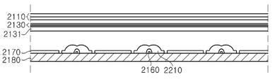
- FIG. 23 is a cross-sectional view illustrating an example in which a light emitting diode package manufactured by a light emitting diode package manufacturing method according to an embodiment of the present invention is applied to a display device.
- the display device includes a display panel 2110, a backlight unit BLU1 that provides light to the display panel 2110, and a panel guide 2100 that supports a lower edge of the display panel 2110.
- the display panel 2110 is not particularly limited and may be, for example, a liquid crystal display panel including a liquid crystal layer.
- a gate driving PCB for supplying a driving signal to the gate line may be further located at the edge of the display panel 2110.
- the gate driving PCBs 2112 and 2113 may be formed on the thin film transistor substrate without being configured in a separate PCB.
- the backlight unit BLU1 includes a light source module including at least one substrate 2150 and a plurality of light emitting diode packages 2160.
- the backlight unit BLU1 may further include a bottom cover 2180, a reflective sheet 2170, a diffusion plate 2131, and optical sheets 2130.
- the bottom cover 2180 may be opened upward to accommodate the substrate 2150, the LED package 2160, the reflective sheet 2170, the diffusion plate 2131, and the optical sheets 2130.
- the bottom cover 2180 may be combined with the panel guide 2100.
- the substrate 2150 may be disposed under the reflective sheet 2170 and may be disposed in a form surrounded by the reflective sheet 2170.
- the present invention is not limited thereto, and when the reflective material is coated on the surface, the reflective material may be positioned on the reflective sheet 2170.
- the substrate 2150 may be formed in plural, and the plurality of substrates 2150 may be arranged side by side, but the present invention is not limited thereto and may be formed of a single substrate 2150.
- the LED package 2160 may include at least one of the LED packages according to the above-described embodiments of the present invention.
- the light emitting diode packages 2160 may be regularly arranged on the substrate 2150 in a predetermined pattern.
- a lens 2210 may be disposed on each LED package 2160 to improve uniformity of light emitted from the plurality of LED packages 2160.
- the diffusion plate 2131 and the optical sheets 2130 are positioned on the light emitting diode package 2160. Light emitted from the LED package 2160 may be supplied to the display panel 2110 in the form of a surface light source through the diffusion plate 2131 and the optical sheets 2130.
- the LED package manufactured according to the LED package manufacturing method according to the embodiments of the present invention may be applied to the direct type display device as in the present embodiment.
- FIG. 24 is a cross-sectional view for describing an example of applying the LED package to the display device using the LED package manufacturing method according to an embodiment.
- the display device including the backlight unit includes a display panel 3210 on which an image is displayed and a backlight unit BLU2 disposed on a rear surface of the display panel 3210 to irradiate light.
- the display device includes a frame 240 that supports the display panel 3210 and accommodates the backlight unit BLU2, and covers 3240 and 3280 that surround the display panel 3210.
- the display panel 3210 is not particularly limited and may be, for example, a liquid crystal display panel including a liquid crystal layer.
- a gate driving PCB for supplying a driving signal to the gate line may be further located at an edge of the display panel 3210.
- the gate driving PCB is not configured in a separate PCB, but may be formed on the thin film transistor substrate.
- the display panel 3210 may be fixed by covers 3240 and 3280 positioned at upper and lower portions thereof, and the cover 3280 positioned at lower portions thereof may be coupled to the backlight unit BLU2.
- the backlight unit BLU2 that provides light to the display panel 3210 is positioned in parallel with the light source module disposed on one side of the lower cover 3270, a portion of the lower cover 3270, and the light source module. And a light guide plate 3250 for converting point light into surface light.
- the backlight unit BLU2 according to the present exemplary embodiment is disposed on the light guide plate 3250 and is disposed below the light guide plate 3250 and the optical sheets 3230 for diffusing and condensing light.
- a reflective sheet 3260 may be further included to reflect the light toward the display panel 3210.
- the light source module includes a substrate 3220 and a plurality of light emitting diode packages 3110 spaced at regular intervals from one surface of the substrate 3220.
- the substrate 3220 is not limited as long as it supports the LED package 3110 and is electrically connected to the LED package 3110.
- the substrate 3220 may be a printed circuit board.
- the light emitting diode package 3110 may include at least one light emitting diode package according to the above-described embodiments of the present invention.
- Light emitted from the light source module is incident to the light guide plate 3250 and is supplied to the display panel 3210 through the optical sheets 3230. Through the light guide plate 3250 and the optical sheets 3230, the point light sources emitted from the light emitting diode packages 3110 may be transformed into surface light sources.
- the LED package according to the LED package manufacturing method according to the embodiments of the present invention can be applied to the edge type display device as in the present embodiment.
- 25 is a cross-sectional view illustrating an example in which a light emitting diode package according to a method of manufacturing a light emitting diode package according to an embodiment of the present invention is applied to a head lamp.
- the head lamp includes a lamp body 4070, a substrate 4020, a light emitting diode package 4010, and a cover lens 4050. Furthermore, the head lamp may further include a heat dissipation unit 4030, a support rack 4060, and a connection member 4040.
- the substrate 4020 is fixed by the support rack 4060 and spaced apart from the lamp body 4070.
- the substrate 4020 is not limited as long as it is a substrate capable of supporting the light emitting diode package 4010.
- the substrate 4020 may be a substrate having a conductive pattern such as a printed circuit board.
- the light emitting diode package 4010 is positioned on the substrate 4020 and may be supported and fixed by the substrate 4020.
- the LED package 4010 may be electrically connected to an external power source through the conductive pattern of the substrate 4020.
- the LED package 4010 may include at least one LED package according to the above-described embodiments of the present invention.
- the cover lens 4050 is positioned on a path along which light emitted from the LED package 4010 travels.
- the cover lens 4050 may be disposed spaced apart from the light emitting diode package 4010 by the connecting member 4040, and in a direction to provide light emitted from the light emitting diode package 4010. Can be arranged.
- the connection member 4040 may fix the cover lens 4050 with the substrate 4020 and may be disposed to surround the light emitting diode package 4010 to serve as a light guide for providing the light emitting path 4045. .
- connection member 4040 may be formed of a light reflective material or coated with a light reflective material.
- the heat dissipation unit 4030 may include a heat dissipation fin 4031 and / or a heat dissipation fan 4033, and radiate heat generated when the LED package 4010 is driven to the outside.
- the LED package according to the LED package manufacturing method according to the embodiments of the present invention may be applied to the head lamp, in particular, a vehicle head lamp.
Abstract
A method for manufacturing a light emitting diode package comprises: arranging a first solder and a second solder between a substrate and a light emitting diode; and subjecting the first solder and the second solder to a heat treatment to bond the substrate and the light emitting diode, wherein the heat treatment of the first and second solders comprises: a heating step of increasing the temperature of the first and second solders from room temperature to a temperature Tp; a maintenance step of maintaining the temperature Tp; and a cooling step of lowering the temperature Tp, wherein the heating step comprises: a first ramping step of increasing a temperature from room temperature to a temperature TA at a constant speed; a pre-heating step of increasing the temperature from the temperature TA to a temperature TB to impart fluidity to the first and second solders; and a second ramping step of increasing the temperature from the TB to TL at a constant speed, wherein the pre-heating step is performed for 60 seconds to 180 seconds.
Description
본 발명은 발광 다이오드 패키지 제조 방법에 대한 것이며, 구체적으로, 발광 다이오드를 기판에 실장하는 조건에 관한 발광 다이오드 패키지 제조 방법에 대한 것이다.The present invention relates to a method of manufacturing a light emitting diode package, and more particularly, to a method of manufacturing a light emitting diode package relating to conditions for mounting a light emitting diode on a substrate.
발광 다이오드(LED)는 전기적 에너지를 광으로 변환하는 고체 상태 소자이다. 발광 다이오드는 백라이트 등에 사용하는 각종 광원, 조명, 신호기, 대형 디스플레이 등에 폭넓게 이용되고 있으며, 회로기판, 봉지재 등과 함께 발광 다이오드 패키지 형태로 사용될 수 있다. 발광 다이오드(LED)는 솔더 등을 통해 회로기판에 실장될 수 있다. 이 때, 양극과 음극이 솔더 내 용제(solvent)에 의해 단락(short)되어, 발광 다이오드 패키지에 불량이 발생할 수 있다. 따라서, 이와 같은 문제를 방지하기 위해, 솔더를 통해 발광 다이오드가 회로기판에 실장될 시의 최적의 조건이 요구되고 있다.Light emitting diodes (LEDs) are solid state devices that convert electrical energy into light. The light emitting diode is widely used in various light sources, lighting, signaling devices, large displays, and the like used in a backlight, and may be used in the form of a light emitting diode package together with a circuit board and an encapsulant. The light emitting diode (LED) may be mounted on a circuit board through solder or the like. At this time, the anode and the cathode are shorted by a solvent in the solder, and thus a defect may occur in the LED package. Therefore, in order to prevent such a problem, optimal conditions are required when a light emitting diode is mounted on a circuit board through solder.
본 발명이 해결하려는 과제는, 불량률이 줄어든 발광 다이오드 패키지 제조 방법을 제공하는 것이다. The problem to be solved by the present invention is to provide a method of manufacturing a light emitting diode package with a reduced defective rate.
본 발명의 일 실시예에 따른 발광 다이오드 패키지 제조 방법은, 기판의 제1 접속 패드 및 제2 접속 패드와 발광 다이오드의 제1 패드 전극 및 제2 패드 전극 사이에 각각 제1 솔더 및 제2 솔더를 배치하고; 상기 제1 및 제2 솔더를 열처리하여 상기 기판과 상기 발광 다이오드를 접합시키는 것을 포함하되, 상기 제1 및 제2 솔더를 열처리하는 것은, 상기 제1 및 제2 솔더를 상온에서 온도 Tp까지 온도를 상승시키는 가열 단계; 온도 Tp에 유지하는 유지 단계; 및 온도 Tp에서 온도를 낮추는 냉각 단계를 포함하고, 상기 가열 단계는, 상온에서 온도 TA까지 일정한 속도로 온도를 상승시키는 제1 램핑 단계; 온도 TA에서 온도 TB까지 온도를 상승시켜 상기 제1 및 제2 솔더에 유동성을 부여하는 예열 단계; 및 TB에서 TL까지 일정한 속도로 온도를 상승시키는 제2 램핑 단계를 포함하며, 상기 예열 단계는 60초 내지 180초 동안 수행된다.In a method of manufacturing a light emitting diode package according to an embodiment of the present invention, a first solder and a second solder are respectively disposed between a first connection pad and a second connection pad of a substrate, and a first pad electrode and a second pad electrode of a light emitting diode. To place; And heat-treating the first and second solders to bond the substrate and the light emitting diode to each other, wherein heat-treating the first and second solders includes: heating the first and second solders from room temperature to a temperature Tp; Raising heating step; A holding step of maintaining at a temperature Tp; And a cooling step of lowering the temperature at the temperature Tp, wherein the heating step comprises: a first ramping step of raising the temperature at a constant rate from room temperature to the temperature T A ; A preheating step of increasing the temperature from the temperature T A to the temperature T B to impart fluidity to the first and second solders; And a second ramping step of raising the temperature at a constant rate from T B to T L , wherein the preheating step is performed for 60 to 180 seconds.
나아가, 상기 예열 단계는 온도 상승 속도가 시간에 따라 변하는 구간을 포함할 수 있다. 상기 예열 단계는 또한 온도 상승 속도가 일정한 구간을 포함할 수도 있다.In addition, the preheating step may include a section in which the rate of temperature rise changes with time. The preheating step may also include a section in which the rate of temperature rise is constant.
상기 예열 단계는 150도 내지 200도의 온도 범위에서 온도를 상승시킬 수 있다. 예를 들어, 상기 온도 TA는 150도이고, 상기 온도 TB는 200도일 수 있다.The preheating step may increase the temperature in the temperature range of 150 degrees to 200 degrees. For example, the temperature T A may be 150 degrees, and the temperature T B may be 200 degrees.
한편, 상기 온도 Tp는 300도 이하일 수 있다. 더 구체적으로, 상기 온도 Tp는 260도일 수 있다.On the other hand, the temperature Tp may be 300 degrees or less. More specifically, the temperature Tp may be 260 degrees.
한편, 상기 제2 램핑 단계 후에 솔더에 점착성이 부여되는 솔더링이 진행되되, 상기 솔더링은 상기 가열 단계 중 상기 온도 TL에서 상기 온도 Tp까지 상승하는 단계 및 상기 유지 단계 그리고, 상기 냉각 단계의 일부에서 진행될 수 있다.Meanwhile, after the second ramping step, a soldering process is performed in which adhesiveness is imparted to the solder, and the soldering process may be performed in the step of increasing the temperature TL from the temperature TL to the temperature Tp during the heating step, the holding step, and the cooling step. Can be.
나아가, 상기 온도 TL에서 상기 온도 Tp까지 상승하는 단계는 3℃/초 이하의 속도로 온도가 상승할 수 있으며, 상기 솔더링이 진행되는 냉각 단계는 6℃/초 이하의 속도로 온도가 하강할 수 있다.Further, the step of increasing from the temperature TL to the temperature Tp may increase the temperature at a rate of 3 ° C / sec or less, and the cooling step in which the soldering proceeds may lower the temperature at a rate of 6 ° C / sec or less. have.
또한, 상기 솔더링은 217도 내지 260도 온도 범위에서 88초 내지 90초간 수행될 수 있다. 나아가, 상기 제1 솔더 및 상기 제2 솔더는 상기 제1 솔더 및 상기 제2 솔더 전체 질량의 1% 내지 1.4%의 Ag을 포함할 수 있다.In addition, the soldering may be performed for 88 seconds to 90 seconds in the temperature range of 217 degrees to 260 degrees. Further, the first solder and the second solder may include 1% to 1.4% Ag of the total mass of the first solder and the second solder.
한편, 상기 제1 솔더 및 제2 솔더를 배치하는 것은, 상기 제1 접속 패드 및 제2 접속 패드를 각각 노출시키는 제1 노출 영역 및 제2 노출 영역을 갖는 마스크를 상기 기판 상에 배치하고, 상기 마스크의 제1 노출 영역 및 제2 노출 영역에 상기 제1 및 제2 솔더를 배치하는 것을 포함할 수 있다.On the other hand, disposing the first solder and the second solder, a mask having a first exposed area and a second exposed area for exposing the first connection pad and the second connection pad, respectively, on the substrate, The method may include disposing the first and second solder in the first exposed area and the second exposed area of the mask.
상기 마스크의 두께는 0.08mm 내지 0.18mm일 수 있다.The thickness of the mask may be 0.08 mm to 0.18 mm.
또한, 상기 제1 노출 영역의 넓이 및 상기 제2 노출 영역의 넓이는 각각 상기 제1 접속 패드의 상면 면적 및 상기 제2 접속 패드의 상면 면적의 80% 내지 110%일 수 있다.The area of the first exposure area and the area of the second exposure area may be 80% to 110% of the top surface area of the first connection pad and the top surface area of the second connection pad, respectively.
상기 제1 노출 영역의 중심 및 상기 제2 노출 영역의 중심은 각각 상기 제1 접속 패드의 상면의 중심 및 상기 제2 접속 패드의 상면의 중심과 상하 방향으로 중첩할 수 있다.The center of the first exposure area and the center of the second exposure area may respectively overlap the center of the top surface of the first connection pad and the center of the top surface of the second connection pad in the vertical direction.
또한, 상기 제1 솔더의 양 및 제2 솔더의 양은 각각 기준 솔더 양의 100% 내지 150%이며, 상기 기준 솔더 양은 하기 식 1에 따른 부피일 수 있다.In addition, the amount of the first solder and the amount of the second solder may be 100% to 150% of the reference solder amount, respectively, and the reference solder amount may be a volume according to Equation 1 below.
[식 1][Equation 1]
기준 솔더 양(mm3) = (상기 제1 노출 영역의 상면 영역(mm2) 및 상기 제2 노출 영역 상면 영역(mm2))× 0.08mmBased on the solder amount (mm 3) = (the first top surface area of the exposed area (mm 2) and said second exposed region top surface area (mm 2)) × 0.08mm
일 실시예에서, 상기 기판은 상기 제1 접속 패드 및 상기 제2 접속 패드 사이에 위치하며, 상기 제1 접속 패드 및 상기 제2 접속 패드와 나란하며, 상기 기판의 상면이 일부 함몰되어 형성된 홈부를 포함할 수 있다.In an embodiment, the substrate is positioned between the first connection pad and the second connection pad, is parallel to the first connection pad and the second connection pad, and has a groove formed by partially recessed an upper surface of the substrate. It may include.
다른 실시예에서, 상기 기판은 상기 제1 접속 패드 및 상기 제2 접속 패드 사이에 위치하며, 상기 기판의 상면부터 상기 기판의 하면을 관통하는 적어도 하나의 홀을 포함할 수 있다. 또 다른 실시예에서, 상기 기판은 상기 홈부와 함께 상기 홀을 포함할 수도 있다.In another embodiment, the substrate may be positioned between the first connection pad and the second connection pad, and may include at least one hole penetrating through the lower surface of the substrate from an upper surface of the substrate. In another embodiment, the substrate may include the hole together with the groove.
상기 발광 다이오드 패키지 제조 방법은, 상기 제1 패드 전극 및 상기 제2 패드 전극을 갖는 발광 다이오드를 제조하는 단계를 더 포함할 수 있으며, 상기 발광 다이오드를 제조하는 단계는, 성장 기판 상에 제1 도전형 반도체층, 제2 도전형 반도체층 및 상기 제1 도전형 반도체층과 상기 제2 도전형 반도체층 사이에 위치하는 활성층을 포함하는 발광 구조체를 형성하는 단계; 상기 제1 도전형 반도체층 및 상기 제2 도전형 반도체층에 각각 오믹 컨택하는 제1 컨택 전극 및 제2 컨택 전극을 형성하는 단계; 상기 제1 컨택 전극 및 상기 제2 컨택 전극을 절연시키며, 상기 제1 컨택및 상기 2 컨택 전극을 부분적으로 덮는 절연층을 형성하는 단계; 및 상기 절연층 상에 상기 제1 컨택 전극 및 상기 제2 컨택 전극 각각에 전기적으로 연결된 제1 패드 전극 및 제2 패드 전극을 형성하는 단계를 포함할 수 있다. 나아가, 상기 제2 컨택 전극은 Ag를 포함할 수 있다.The method of manufacturing a light emitting diode package may further include manufacturing a light emitting diode having the first pad electrode and the second pad electrode. The manufacturing of the light emitting diode may include a first conductive layer on a growth substrate. Forming a light emitting structure including a type semiconductor layer, a second conductivity type semiconductor layer, and an active layer positioned between the first conductivity type semiconductor layer and the second conductivity type semiconductor layer; Forming a first contact electrode and a second contact electrode in ohmic contact with the first conductive semiconductor layer and the second conductive semiconductor layer, respectively; Forming an insulating layer to insulate the first contact electrode and the second contact electrode and partially cover the first contact and the second contact electrode; And forming a first pad electrode and a second pad electrode electrically connected to each of the first contact electrode and the second contact electrode on the insulating layer. Furthermore, the second contact electrode may include Ag.
본 발명에 따르면, 솔더 내에 함유된 용제를 충분히 제거하여 발광 다이오드 패키지 내에 단락이 발생하는 것을 방지할 수 있다. 이에 따라, 발광 다이오드 패키지의 불량률이 줄어들 수 있다.According to the present invention, the solvent contained in the solder can be sufficiently removed to prevent the short circuit from occurring in the light emitting diode package. Accordingly, the defective rate of the LED package can be reduced.
도 1 내지 도 17은 본 발명의 일 실시예에 따른 발광 다이오드 패키지 제조 방법을 설명하기 위한 평면도들 및 단면도들이다.1 to 17 are plan views and cross-sectional views illustrating a method of manufacturing a light emitting diode package according to an embodiment of the present invention.
도 18 내지 도 21은 본 발명의 일 실시예에 따른 발광 다이오드 패키지 제조 방법에 따른 발광 다이오드 패키지의 불량률을 설명하기 위한 그래프들이다.18 to 21 are graphs for describing a defective rate of the LED package according to the LED package manufacturing method according to an embodiment of the present invention.
도 22은 본 발명의 일 실시예에 따른 발광 다이오드 패키지 제조 방법에 의해 제조된 발광 다이오드 패키지를 조명 장치에 적용한 예를 설명하기 위한 분해 사시도이다.22 is an exploded perspective view illustrating an example in which a light emitting diode package manufactured by a light emitting diode package manufacturing method according to an embodiment of the present invention is applied to a lighting device.
도 23은 본 발명의 일 실시예에서 따른 발광 다이오드 패키지 제조 방법에 의해 제조된 발광 다이오드 패키지를 디스플레이 장치에 적용한 예를 설명하기 위한 단면도이다.FIG. 23 is a cross-sectional view illustrating an example in which a light emitting diode package manufactured by a light emitting diode package manufacturing method according to an embodiment of the present invention is applied to a display device.
도 24는 본 발명의 일 실시예에 따른 발광 다이오드 패키지 제조 방법에 의해 제조된 발광 다이오드 패키지를 디스플레이 장치에 적용한 예를 설명하기 위한 단면도이다.24 is a cross-sectional view illustrating an example in which a light emitting diode package manufactured by a light emitting diode package manufacturing method according to an embodiment of the present invention is applied to a display device.
도 25는 본 발명의 일 실시예에 따른 발광 다이오드 패키지 제조 방법에 의해 제조된 발광 다이오드 패키지를 헤드 램프에 적용한 예를 설명하기 위한 단면도이다.25 is a cross-sectional view illustrating an example in which a light emitting diode package manufactured by a light emitting diode package manufacturing method according to an embodiment of the present invention is applied to a head lamp.
이하, 첨부한 도면들을 참조하여 본 발명의 실시예들을 상세히 설명한다. 다음에 소개되는 실시예들은 본 발명이 속하는 기술분야의 통상의 기술자에게 본 발명의 사상이 충분히 전달될 수 있도록 하기 위해 예로서 제공되는 것이다. 따라서, 본 발명은 이하 설명되는 실시예들에 한정되지 않고 다른 형태로 구체화될 수도 있다. 그리고, 도면들에 있어서, 구성요소의 폭, 길이, 두께 등은 편의를 위하여 과장되어 표현될 수도 있다. 또한, 하나의 구성요소가 다른 구성요소의 "상부에" 또는 "상에" 있다고 기재된 경우 각 부분이 다른 부분의 "바로 상부" 또는 "바로 상에" 있는 경우뿐만 아니라 각 구성요소와 다른 구성요소 사이에 또 다른 구성요소가 개재된 경우도 포함한다. 명세서 전체에 걸쳐서 동일한 참조번호들은 동일한 구성요소들을 나타낸다.Hereinafter, with reference to the accompanying drawings will be described embodiments of the present invention; The following embodiments are provided as examples to sufficiently convey the spirit of the present invention to those skilled in the art to which the present invention pertains. Accordingly, the present invention is not limited to the embodiments described below and may be embodied in other forms. In the drawings, widths, lengths, thicknesses, and the like of components may be exaggerated for convenience. In addition, when one component is described as "on" or "on" another component, each component is different from each other as well as when the component is "just above" or "on" the other component. It also includes a case where another component is interposed therebetween. Like numbers refer to like elements throughout.
도 1 내지 도 17은 본 발명의 일 실시예에 따른 발광 다이오드 패키지 제조 방법을 설명하기 위한 평면도들, 단면도들 및 그래프이다. 각 도면들에 있어서, (b)에 도시된 단면도는 (a)에 도시된 평면도의 A-A'선에 대응하는 부분의 단면을 나타낸다.도 1 내지 도 17은 본 실시예에 따른 발광 다이오드 패키지 제조 방법을 설명하기 위하여 참조되나, 본 실시예의 발광 다이오드 제조 방법이 도면들의 순서에 제한되는 것은 아니다.1 to 17 are plan views, cross-sectional views and graphs for describing a method of manufacturing a light emitting diode package according to an embodiment of the present invention. In each of the drawings, the cross-sectional view shown in (b) shows a cross section of a portion corresponding to the line A-A 'of the plan view shown in (a). FIGS. 1 to 17 show light emitting diode packages according to the present embodiment. Reference is made to explain the manufacturing method, but the light emitting diode manufacturing method of the present embodiment is not limited to the order of the drawings.
먼저, 도 1 및 도 2를 참조하면, 성장 기판(110) 상에 발광 구조체(120)를 형성하여 웨이퍼(W1)를 준비한다.First, referring to FIGS. 1 and 2, the light emitting structure 120 is formed on the growth substrate 110 to prepare the wafer W1.
도 1을 참조하면, 웨이퍼(W1)는 성장 기판(110) 및 성장 기판(110) 상에 성장된 발광 구조체(120)를 포함할 수 있다. 또한, 하나의 웨이퍼(W1)로부터 복수의 발광 다이오드들이 제조될 수 있고, 따라서, 웨이퍼(W1)는 복수의 단위 발광 다이오드 영역(UD1)을 포함할 수 있다. 설명의 편의를 위하여, 도 2 내지 도 17을 참조하여 설명하는 경우, 단위 발광 다이오드 영역(UD1)에서의 발광 다이오드 제조 방법을 설명한다. 즉, 본 실시예의 제조 방법은 복수의 단위 발광 다이오드 영역(UD1)을 포함하는 웨이퍼(W1) 전체에 걸쳐 적용될 수 있다.Referring to FIG. 1, the wafer W1 may include a growth substrate 110 and a light emitting structure 120 grown on the growth substrate 110. In addition, a plurality of light emitting diodes may be manufactured from one wafer W1, and thus, the wafer W1 may include a plurality of unit light emitting diode regions UD1. For convenience of description, the light emitting diode manufacturing method in the unit light emitting diode region UD1 will be described with reference to FIGS. 2 to 17. That is, the manufacturing method of the present embodiment may be applied to the entire wafer W1 including the plurality of unit light emitting diode regions UD1.
도 2를 참조하면, 성장 기판(110) 상에 제1 도전형 반도체층(121), 활성층(123) 및 제2 도전형 반도체층(125)을 포함하는 발광 구조체(120)를 형성한다.Referring to FIG. 2, a light emitting structure 120 including a first conductive semiconductor layer 121, an active layer 123, and a second conductive semiconductor layer 125 is formed on the growth substrate 110.
성장 기판(110)은 발광 구조체(120)를 성장시킬 수 있는 기판이면 한정되지 않는다. 예를 들어, 성장 기판(110)은 사파이어 기판, 실리콘 카바이드 기판, 실리콘 기판, 질화갈륨 기판, 질화알루미늄 기판 등일 수 있다. 또한, 성장 기판(110)은 그 상면에 형성된 요철 패턴을 포함할 수도 있다. 성장 기판(110)은 이 후, 별도의 공정을 통해 발광 다이오드로부터 제거될 수도 있다.The growth substrate 110 is not limited as long as it is a substrate capable of growing the light emitting structure 120. For example, the growth substrate 110 may be a sapphire substrate, a silicon carbide substrate, a silicon substrate, a gallium nitride substrate, an aluminum nitride substrate, or the like. In addition, the growth substrate 110 may include an uneven pattern formed on an upper surface thereof. The growth substrate 110 may then be removed from the light emitting diode through a separate process.
발광 구조체(120)는 유기금속화학증착(Metal-organic chemical vapor deposition; MOCVD), 수소화물기상증착(Hydride vapor phase epitaxy; HVPE), 또는 분자선 증착(Molecular beam epitaxy; MBE) 등의 방법을 이용하여 성장 기판(110) 상에 성장될 수 있다. 발광 구조체(120)는 제1 도전형 반도체층(121), 활성층(123) 및 제2 도전형 반도체층(125)을 포함한다. 제1 도전형 반도체층(121), 활성층(123) 및 제2 도전형 반도체층(125) 각각은 Ⅲ-Ⅴ계열 화합물 반도체를 포함할 수 있고, 예를 들어, (Al, Ga, In)N과 같은 질화물계 반도체를 포함할 수 있다. 제1 도전형 반도체층(121)은 n형 불순물(예를 들어, Si)을 포함하여 n형의 도전형을 가질 수 있고, 제2 도전형 반도체층(125)은 p형 불순물(예를 들어, Mg)을 포함하여 p형의 도전형을 가질 수 있다. 또한, 제1 및 제2 도전형 반도체층(121, 125)의 도전형은 상술한 바와 반대일 수도 있다. 활성층(123)은 다중양자우물 구조(MQW)를 포함할 수 있고, 원하는 피크 파장의 광을 방출하도록 그 조성비가 결정될 수 있다. 예를 들어, 활성층(123)은, UV 파장 대역의 피크 파장을 갖는 광 또는 청색 파장 대역의 피크 파장을 갖는 광을 방출할 수 있다.The light emitting structure 120 may be formed using a method such as metal-organic chemical vapor deposition (MOCVD), hydride vapor phase epitaxy (HVPE), or molecular beam deposition (MBE). It may be grown on the growth substrate 110. The light emitting structure 120 includes a first conductive semiconductor layer 121, an active layer 123, and a second conductive semiconductor layer 125. Each of the first conductive semiconductor layer 121, the active layer 123, and the second conductive semiconductor layer 125 may include a III-V-based compound semiconductor. For example, (Al, Ga, In) N It may include a nitride-based semiconductor such as. The first conductivity-type semiconductor layer 121 may have an n-type conductivity type including n-type impurity (eg, Si), and the second conductivity-type semiconductor layer 125 may have a p-type impurity (for example It may have a p-type conductivity type, including Mg). In addition, the conductivity types of the first and second conductivity-type semiconductor layers 121 and 125 may be opposite to those described above. The active layer 123 may include a multi-quantum well structure (MQW), and its composition ratio may be determined to emit light of a desired peak wavelength. For example, the active layer 123 may emit light having a peak wavelength in the UV wavelength band or light having a peak wavelength in the blue wavelength band.
이어서, 도 3을 참조하면, 발광 구조체(120)를 패터닝하여 제1 도전형 반도체층(121)이 부분적으로 노출된 영역을 형성한다. 예를 들어, 도 2에 도시된 바와 같이, 적어도 하나의 메사(120m)를 형성함으로써, 제1 도전형 반도체층(121)이 부분적으로 노출된 영역을 형성할 수 있다.Subsequently, referring to FIG. 3, the light emitting structure 120 is patterned to form a region in which the first conductive semiconductor layer 121 is partially exposed. For example, as shown in FIG. 2, by forming at least one mesa 120m, a region in which the first conductivity type semiconductor layer 121 is partially exposed may be formed.
메사(120m)는 사진 및 식각 공정을 통해 제2 도전형 반도체층(125) 및 활성층(123)을 부분적으로 제거함으로써 형성될 수 있다. 메사(120m) 주변 영역에는 제1 도전형 반도체층(121)이 부분적으로 노출될 수 있다. 메사(120m)의 형태는 제한되지 않으나, 예를 들어, 도 3(a)에 도시된 바와 같이, 대체로 동일한 방향으로 기다랗게 연장되는 형태로 형성될 수 있으며, 또한, 복수로 형성될 수 있다. 이 경우, 복수의 메사들(120m)은 서로 이격된다.The mesa 120m may be formed by partially removing the second conductivity-type semiconductor layer 125 and the active layer 123 through photolithography and etching processes. The first conductivity-type semiconductor layer 121 may be partially exposed in an area around the mesa 120m. The shape of the mesa 120m is not limited, but, for example, as shown in FIG. 3A, the mesa 120m may be formed to elongate in the same direction and may be formed in plural. In this case, the plurality of mesas 120m are spaced apart from each other.
본 발명은 이에 한정되지 않으며, 도 4의 (a) 및 (b)에 도시된 바와 같이, 메사(120m)는 일체로 형성되되, 상기 메사(120m)의 일 측면으로부터 함입되는 부분을 갖는 형태를 가질 수도 있다. 예컨대, 도 4의 (a)에 도시된 바와 같이, 메사(120m)는 성장 기판(110)의 일 측면에 인접하는 부분에서 서로 연결되고, 상기 일 측면에 반대하여 위치하는 타 측면에 인접하는 부분에는 이격 영역이 형성된 형태로 형성될 수 있다. 상기 이격 영역을 통해 제1 도전형 반도체층(121)이 부분적으로 노출될 수 있다. 상기 이격 영역은 복수로 형성될 수 있으며, 도 4의 (a)와 같이 2개로 형성될 수도 있으나, 3개 이상으로 형성될 수도 있다. 한편, 이와 달리, 도 4(b)에 도시된 바와 같이, 발광 구조체(120)는 제1 도전형 반도체층(121)을 부분적으로 노출시키는 적어도 하나의 홀(120h)을 포함할 수도 있다. 상기 홀(120h)은 복수로 형성될 수 있으며, 규칙적으로 배치될 수 있다.The present invention is not limited thereto, and as shown in FIGS. 4A and 4B, the mesas 120m are integrally formed and have a portion recessed from one side of the mesas 120m. May have For example, as shown in FIG. 4A, the mesas 120m are connected to each other at a portion adjacent to one side of the growth substrate 110 and a portion adjacent to the other side positioned opposite to the one side. It may be formed in the form in which the spaced area is formed. The first conductivity type semiconductor layer 121 may be partially exposed through the separation region. The separation region may be formed in plural, and may be formed in two as shown in FIG. 4A, but may be formed in three or more. On the other hand, as shown in FIG. 4B, the light emitting structure 120 may include at least one hole 120h partially exposing the first conductivity-type semiconductor layer 121. The hole 120h may be formed in plural and regularly arranged.
다음, 도 5를 참조하면, 제2 도전형 반도체층(125) 상에, 즉, 메사(120m) 상면의 적어도 일부 상에 제2 컨택 전극(140)을 형성한다. 나아가, 발광 구조체(120) 상에 예비(pre) 제1 절연층(151)을 더 형성할 수 있다.Next, referring to FIG. 5, the second contact electrode 140 is formed on the second conductivity-type semiconductor layer 125, that is, on at least a portion of the upper surface of the mesa 120m. In addition, a pre-first insulating layer 151 may be further formed on the light emitting structure 120.
제2 컨택 전극(140)은, 제2 도전형 반도체층(125)에 오믹 컨택할 수 있는 물질로 형성될 수 있고, 예를 들어, 금속성 물질 및/또는 도전성 산화물을 포함할 수 있다.The second contact electrode 140 may be formed of a material capable of ohmic contact with the second conductivity type semiconductor layer 125 and may include, for example, a metallic material and / or a conductive oxide.
제2 컨택 전극(140)이 금속성 물질을 포함하는 경우, 제2 컨택 전극(140)은 반사층 및 상기 반사층을 덮는 커버층을 포함할 수 있다. 상술한 바와 같이, 제2 컨택 전극(140)은 제2 도전형 반도체층(125)과 오믹 컨택되는 것과 더불어, 광을 반사시키는 기능을 할 수 있다. 따라서, 상기 반사층은 높은 반사도를 가지면서 제2 도전형 반도체층(125)과 오믹 접촉을 형성할 수 있는 금속을 포함할 수 있다. 예를 들어, 상기 반사층은 Ni, Pt, Pd, Rh, W, Ti, Al, Mg, Ag 및 Au 중 적어도 하나를 포함할 수 있다. 또한, 상기 반사층은 단일층 또는 다중층을 포함할 수 있다.When the second contact electrode 140 includes a metallic material, the second contact electrode 140 may include a reflective layer and a cover layer covering the reflective layer. As described above, the second contact electrode 140 may function to reflect light while being in ohmic contact with the second conductivity-type semiconductor layer 125. Therefore, the reflective layer may include a metal having high reflectivity and capable of forming ohmic contact with the second conductivity-type semiconductor layer 125. For example, the reflective layer may include at least one of Ni, Pt, Pd, Rh, W, Ti, Al, Mg, Ag, and Au. In addition, the reflective layer may include a single layer or multiple layers.
상기 커버층은 상기 반사층과 다른 물질 간의 상호 확산을 방지할 수 있고, 외부의 다른 물질이 상기 반사층에 확산하여 상기 반사층이 손상되는 것을 방지할 수 있다. 따라서, 상기 커버층은 상기 반사층의 하면 및 측면을 덮도록 형성될 수 있다. 상기 커버층은 상기 반사층과 함께 제2 도전형 반도체층(125)과 전기적으로 연결될 수 있어서, 상기 반사층과 함께 전극 역할을 할 수 있다. 상기 커버층은, 예를 들어, Au, Ni, Ti, Cr 등을 포함할 수 있으며, 단일층 또는 다중층을 포함할 수도 있다. The cover layer may prevent mutual diffusion between the reflective layer and another material, and prevent other external materials from diffusing into the reflective layer and damaging the reflective layer. Thus, the cover layer may be formed to cover the bottom and side surfaces of the reflective layer. The cover layer may be electrically connected to the second conductivity-type semiconductor layer 125 together with the reflective layer, and serve as an electrode together with the reflective layer. The cover layer may include, for example, Au, Ni, Ti, Cr, or the like, and may include a single layer or multiple layers.
이러한 반사층 및 커버층은 전자선 증착, 도금 방식 등을 이용하여 형성될 수 있다. The reflective layer and the cover layer may be formed using electron beam deposition, plating, or the like.
한편, 제2 컨택 전극(140)이 도전성 산화물을 포함하는 경우, 상기 도전성 산화물은 ITO, ZnO, AZO, IZO 등일 수 있다. 제2 컨택 전극(140)이 도전성 산화물을 포함하는 경우, 금속을 포함하는 경우에 비해 더 넓은 영역의 제2 도전형 반도체층(125)의 상면을 커버할 수 있다. 즉, 제1 도전형 반도체층(121)이 노출된 영역의 테두리로부터 제2 컨택 전극(140)까지의 이격 거리는 제2 컨택 전극(140)이 도전성 산화물로 형성된 경우에 상대적으로 더 짧게 형성될 수 있다. 이 경우, 제2 컨택 전극(140)과 제2 도전형 반도체층(125)이 접촉하는 부분에서 제1 컨택 전극(130)과 제1 도전형 반도체층(121)이 접촉하는 부분까지의 최단 거리가 상대적으로 더 짧아질 수 있어서, 발광 다이오드의 순방향 전압(Vf)이 감소될 수 있다.Meanwhile, when the second contact electrode 140 includes a conductive oxide, the conductive oxide may be ITO, ZnO, AZO, IZO, or the like. When the second contact electrode 140 includes the conductive oxide, the second contact electrode 140 may cover the upper surface of the second conductive semiconductor layer 125 in a wider area than when the metal includes the conductive oxide. That is, the separation distance from the edge of the region where the first conductivity type semiconductor layer 121 is exposed to the second contact electrode 140 may be formed to be relatively shorter when the second contact electrode 140 is formed of a conductive oxide. have. In this case, the shortest distance from the contact portion of the second contact electrode 140 to the second conductivity type semiconductor layer 125 to the contact portion of the first contact electrode 130 and the first conductivity type semiconductor layer 121. Can be made relatively shorter, so that the forward voltage V f of the light emitting diode can be reduced.
이는 금속성 물질로 제2 컨택 전극(140)을 형성하는 경우와, 도전성 산화물로 제2 컨택 전극(140)을 형성하는 경우의 제조 방법 차이로부터 기인한 것일 수 있다. 예를 들어, 금속성 물질은 증착 또는 도금 방식으로 형성되므로, 마스크의 공정 마진에 의해 제2 도전형 반도체층(125)의 외곽 테두리(메사(120m)의 외곽 테두리)로부터 일정 거리 이격된 부분에 형성된다. 반면, 도전성 산화물은 제2 도전형 반도체층(125) 상에 전체적으로 형성된 후에, 제1 도전형 반도체층(121)을 노출시키는 식각 공정에서 동일 공정으로 제거된다. 따라서, 도전성 산화물은 상대적으로 제2 도전형 반도체층(125)의 외곽 테두리에 더욱 가깝게 형성될 수 있다. 다만, 본 발명이 이에 한정되는 것은 아니다.This may be due to the difference in the manufacturing method between forming the second contact electrode 140 with the metallic material and forming the second contact electrode 140 with the conductive oxide. For example, since the metallic material is formed by a deposition or plating method, the metal material is formed at a portion spaced from the outer edge of the second conductive semiconductor layer 125 (the outer edge of the mesa 120m) by a process margin of the mask. do. On the other hand, the conductive oxide is entirely formed on the second conductive semiconductor layer 125, and then removed in the same process in the etching process of exposing the first conductive semiconductor layer 121. Therefore, the conductive oxide may be formed relatively closer to the outer edge of the second conductivity type semiconductor layer 125. However, the present invention is not limited thereto.
제2 컨택 전극(140)이 ITO 또는 ZnO등과 같은 투명 전극으로 이루어지거나 투명 전극을 포함하는 경우, 제1 절연층(150)은 분포 브래그 반사기를 포함하여 광을 발광 구조체(120)으로부 반사시켜 발광 효율을 향상시킬 수 있다. 또한, 제2 컨택 전극(140)이 ITO를 포함하고, 제1 절연층(150)이 SiO2
또는 DBR을 포함하며, 제1 컨택 전극(130)이 Al과 같은 반사층을 포함하는 경우, ITO/SiO2(또는 DBR)/Al 적층 구조를 포함하는 전방위 반사기가 형성될 수 있다. 나아가, 제2 컨택 전극(140)은 도전성 산화물 및 금속층을 모두 포함할 수 있다. 이 경우, 제2 컨택 전극(140)은 제2 도전형 반도체층(125)과 오믹 컨택하는 도전성 산화물 및 도전성 산화물 상에 위치하는 금속층을 포함할 수 있고, 이때, 금속층은 광 반사성을 갖는 반사층일 수 있다.When the second contact electrode 140 is made of a transparent electrode such as ITO or ZnO, or includes a transparent electrode, the first insulating layer 150 includes a distribution Bragg reflector to reflect light from the light emitting structure 120. The luminous efficiency can be improved. In addition, the second contact electrode 140 includes ITO, and the first insulating layer 150 is SiO 2. Alternatively, when the first contact electrode 130 includes a reflective layer such as Al, the omnidirectional reflector including the ITO / SiO 2 (or DBR) / Al stacked structure may be formed. In addition, the second contact electrode 140 may include both a conductive oxide and a metal layer. In this case, the second contact electrode 140 may include a conductive oxide in ohmic contact with the second conductive semiconductor layer 125 and a metal layer on the conductive oxide, wherein the metal layer is a reflective layer having light reflectivity. Can be.
한편, 예비 제1 절연층(151)은 발광 구조체(120) 상에 형성되되, 제2 컨택 전극(140)이 형성되는 영역을 제외한 발광 구조체(120)의 상면을 적어도 부분적으로 덮도록 형성될 수 있다. 예비 제1 절연층(151)은 제1 도전형 반도체층(121)이 노출된 영역을 덮을 수 있으며, 나아가, 메사(120m)들의 측면을 더 덮을 수 있으며, 더 나아가, 메사(120m)들의 상면을 부분적으로 덮을 수 있다. 예비 제1 절연층(151)은 제2 컨택 전극(140)과 접촉할 수도 있으며, 이격될 수도 있다. 예비 제1 절연층(151)이 이격되는 경우, 예비 제1 절연층(151)과 제2 컨택 전극(140)의 사이에는 제2 도전형 반도체층(125)이 부분적으로 노출된다. 예비 제1 절연층(151)은 SiO2, SiNx, MgF2
등을 포함할 수 있다. 나아가, 예비 제1 절연층(151)은 다중층을 포함할 수 있고, 굴절률이 다른 물질이 교대로 적층된 분포 브래그 반사기를 포함할 수도 있다.Meanwhile, the preliminary first insulating layer 151 may be formed on the light emitting structure 120, and may be formed to at least partially cover the top surface of the light emitting structure 120 except for the region where the second contact electrode 140 is formed. have. The preliminary first insulating layer 151 may cover an area where the first conductivity type semiconductor layer 121 is exposed, and may further cover side surfaces of the mesas 120m, and further, an upper surface of the mesas 120m. Can be partially covered. The preliminary first insulating layer 151 may contact the second contact electrode 140 or may be spaced apart from each other. When the preliminary first insulating layer 151 is spaced apart from each other, the second conductive semiconductor layer 125 is partially exposed between the preliminary first insulating layer 151 and the second contact electrode 140. The preliminary first insulating layer 151 may be SiO 2 , SiN x , MgF 2 And the like. Furthermore, the preliminary first insulating layer 151 may include multiple layers, and may include a distributed Bragg reflector in which materials having different refractive indices are alternately stacked.
한편, 예비 제1 절연층(151)은 제2 컨택 전극(140)의 형성 전에 형성될 수도 있고, 제2 컨택 전극(140)의 형성 후에 형성될 수도 있으며, 또한 제2 컨택 전극(140)의 형성 중에 형성될 수도 있다. 예컨대, 제2 컨택 전극(140)이 도전성 산화물층 및 상기 도전성 산화물층 상에 위치하는 금속을 포함하는 반사층을 포함하는 경우, 제2 도전형 반도체층(125) 상에 도전성 산화물층을 형성하고, 반사층을 형성하기 전에 예비 제1 절연층(151)을 형성할 수 있다. 이때, 상기 도전성 산화물층은 제2 도전형 반도체층(125)과 오믹 컨택하며, 예비 제1 절연층(151)은 약 1000Å의 두께로 형성될 수 있다. 또 다른 실시예에서, 예비 제1 절연층(151)은 제2 컨택 전극(140)의 형성 전에 형성될 수 있으며, 이 경우, 제2 컨택 전극(140)은 제2 도전형 반도체층(125)과 오믹 컨택을 형성하며, 금속 물질로 형성된 반사층을 포함할 수 있다. 이러한 실시예들에서, 금속 물질을 포함하는 반사층의 형성 전에 예비 제1 절연층(151)을 형성함으로써, 상기 반사층과 발광 구조체(120) 상호 간의 물질 확산에 의해 상기 반사층의 광 반사율 감소 및 저항 증가를 방지할 수 있다. 또한, 금속 물질을 포함하는 반사층의 형성 과정에서, 제2 컨택 전극(140)이 형성되지 않는 다른 부분에 금속 물질이 잔류하여 발생할 수 있는 전기적 쇼트 등의 문제를 방지할 수 있다.Meanwhile, the preliminary first insulating layer 151 may be formed before the formation of the second contact electrode 140, may be formed after the formation of the second contact electrode 140, and the second contact electrode 140 may be formed. It may be formed during formation. For example, when the second contact electrode 140 includes a conductive oxide layer and a reflective layer including a metal located on the conductive oxide layer, a conductive oxide layer is formed on the second conductive semiconductor layer 125. Before forming the reflective layer, the preliminary first insulating layer 151 may be formed. In this case, the conductive oxide layer may be in ohmic contact with the second conductive semiconductor layer 125, and the preliminary first insulating layer 151 may be formed to have a thickness of about 1000 μs. In another embodiment, the preliminary first insulating layer 151 may be formed before the formation of the second contact electrode 140, in which case the second contact electrode 140 is formed of the second conductivity type semiconductor layer 125. And forming an ohmic contact, and may include a reflective layer formed of a metal material. In such embodiments, the preliminary first insulating layer 151 is formed before the formation of the reflective layer including the metal material, thereby reducing light reflectance and increasing resistance of the reflective layer by material diffusion between the reflective layer and the light emitting structure 120. Can be prevented. In addition, in the process of forming the reflective layer including the metal material, it is possible to prevent a problem such as an electrical short caused by the metal material remaining in another portion where the second contact electrode 140 is not formed.
이어서, 도 6을 참조하면, 발광 구조체(120) 상에 제1 절연층(150)을 형성하되, 제1 절연층(150)은 제1 도전형 반도체층(121), 메사(120m) 및 제2 컨택 전극(140)을 부분적으로 덮는다. 또한, 제1 절연층(150)은 제1 도전형 반도체층(125)을 부분적으로 노출시키는 제1 개구부(150a) 및 제2 컨택 전극(140)을 부분적으로 노출시키는 제2 개구부(150b)를 포함할 수 있다.Subsequently, referring to FIG. 6, a first insulating layer 150 is formed on the light emitting structure 120, wherein the first insulating layer 150 is formed of the first conductive semiconductor layer 121, the mesa 120m, and the first insulating layer 150. 2 partially covers the contact electrode 140. In addition, the first insulating layer 150 may include the first opening 150a partially exposing the first conductive semiconductor layer 125 and the second opening 150b partially exposing the second contact electrode 140. It may include.
제1 절연층(150)은 도 5에서 설명한 예비 제1 절연층(151) 및 주(main) 제1 절연층(153)을 포함할 수 있다. 주 제1 절연층(153)은 SiO2, SiNx, MgF2 등을 포함할 수 있고, PECVD, 전자선 증착(E-beam evaporation) 등의 공지의 증착 방법을 통해 형성될 수 있다. 이때, 주 제1 절연층(153)은 제1 도전형 반도체층(121), 메사(120m) 및 제2 컨택 전극(140)을 전체적으로 덮도록 형성된 후, 패터닝 공정을 통해 제1 및 제2 개구부(150a, 150b)를 형성함으로써, 도시된 바와 같은 제1 절연층(150)이 제공될 수 있다. 상기 패터닝 공정은 사진 식각 공정 또는 리프트 오프 공정을 포함할 수 있다. 나아가, 주 제1 절연층(153)은 다중층을 포함할 수 있고, 굴절률이 다른 물질이 교대로 적층된 분포 브래그 반사기를 포함할 수도 있다. 또한, 주 제1 절연층(153)은 예비 제1 절연층(151)에 비해 두꺼운 두께를 가질 수 있다.The first insulating layer 150 may include the preliminary first insulating layer 151 and the main first insulating layer 153 described with reference to FIG. 5. The primary first insulating layer 153 may include SiO 2 , SiN x , MgF 2, or the like, and may be formed through a known deposition method such as PECVD or E-beam evaporation. In this case, the main first insulating layer 153 is formed to cover the first conductive semiconductor layer 121, the mesa 120m and the second contact electrode 140 as a whole, and then, through the patterning process, the first and second openings. By forming 150a and 150b, the first insulating layer 150 as shown may be provided. The patterning process may include a photolithography process or a lift off process. Furthermore, the primary first insulating layer 153 may include multiple layers, and may include a distributed Bragg reflector in which materials having different refractive indices are alternately stacked. In addition, the main first insulating layer 153 may have a thickness thicker than that of the preliminary first insulating layer 151.
제1 개구부(150a)는 적어도 하나로 형성될 수 있고, 예컨대, 메사들(120m) 각각 상에 형성될 수 있다. 또한, 제1 개구부(150a)는 성장 기판(110)의 일 측면에 인접하는 위치에 형성될 수 있다. 제2 개구부(150b)는 메사(120m)들이 연장되는 방향에 따라 기다랗게 연장된 형상으로 형성될 수 있다. 특히, 제2 개구부(150b)는 메사(120m)들의 긴 측면들에 인접하여 형성될 수 있다.The first opening 150a may be formed in at least one, and for example, may be formed on each of the mesas 120m. In addition, the first opening 150a may be formed at a position adjacent to one side of the growth substrate 110. The second opening 150b may be formed to have an elongated shape along the direction in which the mesas 120m extend. In particular, the second opening 150b may be formed adjacent to the long sides of the mesas 120m.
한편, 본 실시예에서, 메사(120m)를 형성한 후, 제2 컨택 전극(140)을 형성하는 것으로 설명하고 있으나, 이와 달리, 제2 컨택 전극(140)이 먼저 형성된 후에 메사(120m)를 형성할 수도 있다. Meanwhile, in the present exemplary embodiment, the second contact electrode 140 is formed after the mesa 120m is formed. Alternatively, the mesa 120m may be formed after the second contact electrode 140 is formed first. It may be formed.
다음, 도 7을 참조하면, 제1 절연층(150) 상에 제1 컨택 전극(130)을 형성한다. 제1 컨택 전극(130)은 제1 개구부(150a)를 통해 노출된 제1 도전형 반도체층(121)과 오믹 컨택할 수 있다. 나아가, 제2 개구부(150b)를 통해 제2 컨택 전극(140)과 전기적으로 접촉되는 연결 전극(145)을 더 형성할 수 있다.Next, referring to FIG. 7, the first contact electrode 130 is formed on the first insulating layer 150. The first contact electrode 130 may be in ohmic contact with the first conductive semiconductor layer 121 exposed through the first opening 150a. In addition, the connection electrode 145 may be further formed to be in electrical contact with the second contact electrode 140 through the second opening 150b.
제1 컨택 전극(130) 및 연결 전극(145)은 공지의 증착 및 패터닝 방법을 통해 형성될 수 있으며, 동시에 형성될 수도 있고, 별개의 공정을 통해 형성될 수도 있다. 제1 컨택 전극(130) 및 연결 전극(145)은 서로 동일한 물질 및 다층 구조로 형성될 수도 있고, 서로 다른 물질 및/또는 다층 구조로 형성될 수도 있다. 제1 컨택 전극(130)과 연결 전극(145)은 서로 이격되며, 이에 따라, 제1 컨택 전극(130)과 제2 컨택 전극(140)은 서로 전기적으로 절연된다.The first contact electrode 130 and the connection electrode 145 may be formed through known deposition and patterning methods, and may be formed at the same time or may be formed through separate processes. The first contact electrode 130 and the connection electrode 145 may be formed of the same material and a multilayer structure, or may be formed of different materials and / or a multilayer structure. The first contact electrode 130 and the connection electrode 145 are spaced apart from each other, whereby the first contact electrode 130 and the second contact electrode 140 are electrically insulated from each other.
상술한 바와 같이, 제1 컨택 전극(130)은 제1 도전형 반도체층(121)과 오믹 컨택함과 아울러, 광을 반사시키는 역할을 할 수 있다. 따라서, 제1 컨택 전극(130)은 Al층과 같은 고반사성 금속층을 포함할 수 있다. 이때, 제1 컨택 전극(130)은 단일층 또는 다중층으로 이루어질 수 있다. 상기 고반사 금속층은 Ti, Cr 또는 Ni 등의 접착층 상에 형성될 수 있다. 다만, 본 발명이 이에 한정되는 것은 아니며, 제1 컨택 전극(130)은 Ni, Pt, Pd, Rh, W, Ti, Al, Mg, Ag 및 Au 중 적어도 하나를 포함할 수도 있다. 연결 전극(145)은, 예를 들어, Ni, Pt, Pd, Rh, W, Ti, Al, Mg, Ag 및 Au 중 적어도 하나를 포함할 수 있다As described above, the first contact electrode 130 may serve to reflect the light while making ohmic contact with the first conductivity-type semiconductor layer 121. Therefore, the first contact electrode 130 may include a highly reflective metal layer such as an Al layer. In this case, the first contact electrode 130 may be formed of a single layer or multiple layers. The highly reflective metal layer may be formed on an adhesive layer such as Ti, Cr, or Ni. However, the present invention is not limited thereto, and the first contact electrode 130 may include at least one of Ni, Pt, Pd, Rh, W, Ti, Al, Mg, Ag, and Au. The connection electrode 145 may include, for example, at least one of Ni, Pt, Pd, Rh, W, Ti, Al, Mg, Ag, and Au.
예를 들어, 제1 컨택 전극(130) 및/또는 연결 전극(145)은 각각 다층 구조를 포함할 수 있다. 상기 다층 구조는, 제1 접착층(오믹 컨택층)/반사층/베리어층/산화방지층/제2 접착층의 적층 구조를 가질 수 있다. 상기 제1 접촉층은 제1 도전형 반도체층(121) 및/또는 제2 컨택 전극(140)에 접촉하며, Ni, Ti, Cr등을 포함할 수 있다. 상기 반사층은 광 반사율이 높은 금속을 포함할 수 있으며, 예컨대, Al, Ag 등을 포함할 수 있다. 상기 베리어층은 상기 반사층의 금속이 상호 확산하는 것을 방지하며, Cr, Co, Ni, Pt, TiN의 단층으로 형성하거나, Ti, Mo, W과 함께 다층으로 형성될 수 있으며, 예컨대, Ti/Ni의 복층 구조를 가질 수 있다. 상기 산화방지층은 상기 산화방지층의 하부에 위치하는 다른 층들의 산화를 방지하며, 산화에 대한 내성이 강한 금속 물질을 포함할 수 있다. 상기 산화방지층은, 예컨대, Au, Pt, Ag등을 포함할 수 있다. 상기 제2 접착층은 제2 절연층(160)과 제1 도전형 반도체층(121)(또는, 제2 절연층(160)과 연결 전극(145)) 간의 접합력을 향상시키기 위하여 채택될 수 있으며, 예컨대, Ti, Ni, Cr 등을 포함할 수 있다. 다만, 본 발명이 이에 한정되는 것은 아니다.For example, the first contact electrode 130 and / or the connection electrode 145 may each include a multilayer structure. The multilayer structure may have a laminated structure of a first adhesive layer (ohmic contact layer) / reflection layer / barrier layer / antioxidant layer / second adhesive layer. The first contact layer contacts the first conductive semiconductor layer 121 and / or the second contact electrode 140, and may include Ni, Ti, Cr, or the like. The reflective layer may include a metal having high light reflectance, and may include, for example, Al, Ag, or the like. The barrier layer prevents the metals of the reflective layer from mutually diffusing, and may be formed of a single layer of Cr, Co, Ni, Pt, TiN, or may be formed in a multilayer with Ti, Mo, and W. For example, Ti / Ni It may have a multilayer structure of. The antioxidant layer prevents oxidation of other layers positioned below the antioxidant layer, and may include a metal material having a strong resistance to oxidation. The antioxidant layer may include, for example, Au, Pt, Ag, and the like. The second adhesive layer may be adopted to improve the bonding force between the second insulating layer 160 and the first conductive semiconductor layer 121 (or the second insulating layer 160 and the connection electrode 145). For example, it may include Ti, Ni, Cr and the like. However, the present invention is not limited thereto.
이와 달리, 연결 전극(145)은 생략될 수도 있다. 도 8에 도시된 바와 같이, 연결 전극(145)이 생략되는 경우, 제2 개구부(150b)를 통해 제2 컨택 전극(140)이 노출된다. 따라서, 이 경우, 후술할 제2 패드 전극(173)은 제2 컨택 전극(140)과 직접적으로 접촉될 수 있다.Alternatively, the connection electrode 145 may be omitted. As shown in FIG. 8, when the connection electrode 145 is omitted, the second contact electrode 140 is exposed through the second opening 150b. Therefore, in this case, the second pad electrode 173, which will be described later, may directly contact the second contact electrode 140.
이어서, 도 9를 참조하면, 제1 컨택 전극(130) 및 연결 전극(145)을 부분적으로 덮는 제2 절연층(160)을 형성한다. 제2 절연층(160)은 제1 컨택 전극(130) 및 연결 전극(145)을 각각 노출시키는 제3 개구부(160a) 및 제4 개구부(160b)를 포함할 수 있다.9, a second insulating layer 160 partially covering the first contact electrode 130 and the connection electrode 145 is formed. The second insulating layer 160 may include a third opening 160a and a fourth opening 160b exposing the first contact electrode 130 and the connection electrode 145, respectively.
제2 절연층(160)은 SiO2, SiNx, MgF2
등을 포함할 수 있으며, PECVD, 전자선 증착(E-beam evaporation) 등의 공지의 증착 방법을 통해 형성될 수 있다. 이때, 제2 절연층(160)은 제1 컨택 전극(130) 및 연결 전극(145)을 전체적으로 덮도록 형성된 후, 패터닝 공정을 통해 제3 및 제4 개구부(160a, 160b)를 형성함으로써, 도시된 바와 같은 제2 절연층(160)이 제공될 수 있다. 상기 패터닝 공정은 사진 식각 공정 또는 리프트 오프 공정을 포함할 수 있다. 나아가, 제2 절연층(160)은 다중층을 포함할 수 있고, 굴절률이 다른 물질이 교대로 적층된 분포 브래그 반사기를 포함할 수도 있다. 제2 절연층(160)의 최상부층은 SiNx로 형성될 수 있다. 제2 절연층(160)의 최상부층이 SiNx로 형성됨으로써, 발광 구조체(120)로 습기가 침투하는 것을 더욱 효과적으로 방지할 수 있다. 또한, 제2 절연층(160)은 제1 절연층(150)에 비해 얇은 두께를 가질 수 있으며, 절연 내압을 확보하기 위하여 약 0.8㎛ 이상의 두께를 가질 수 있다. 다만, 본 발명이 이에 한정되는 것은 아니다.The second insulating layer 160 is SiO 2 , SiN x , MgF 2 And the like, and may be formed through a known deposition method such as PECVD or E-beam evaporation. In this case, the second insulating layer 160 is formed to cover the first contact electrode 130 and the connecting electrode 145 as a whole, and then, by forming the third and fourth openings 160a and 160b through a patterning process, As described above, a second insulating layer 160 may be provided. The patterning process may include a photolithography process or a lift off process. In addition, the second insulating layer 160 may include multiple layers, and may include a distributed Bragg reflector in which materials having different refractive indices are alternately stacked. The uppermost layer of the second insulating layer 160 may be formed of SiN x . Since the uppermost layer of the second insulating layer 160 is formed of SiN x , it is possible to more effectively prevent moisture from penetrating into the light emitting structure 120. In addition, the second insulating layer 160 may have a thickness thinner than that of the first insulating layer 150, and may have a thickness of about 0.8 μm or more in order to secure an insulation breakdown voltage. However, the present invention is not limited thereto.
제3 및 제4 개구부(160a, 160b)는 각각 제1 컨택 전극(130) 및 연결 전극(145)을 노출시켜, 패드 전극들(171, 173)이 제1 컨택 전극(130) 및 제2 컨택 전극(140)에 전기적으로 연결될 수 있는 통로를 제공할 수 있다.The third and fourth openings 160a and 160b expose the first contact electrode 130 and the connection electrode 145, respectively, so that the pad electrodes 171 and 173 form the first contact electrode 130 and the second contact. A passage that may be electrically connected to the electrode 140 may be provided.
도 10을 참조하면, 제2 절연층(160) 상에 제1 패드 전극(171) 및 제2 패드 전극(173)을 형성한다.Referring to FIG. 10, a first pad electrode 171 and a second pad electrode 173 are formed on the second insulating layer 160.
제1 패드 전극(171)은 제2 절연층(160)의 제3 개구부(160a)를 통해 제1 컨택 전극(130)에 접속하고, 제2 패드 전극(173)은 제2 절연층(160)의 제4 개구부(160b)를 통해 제2 컨택 전극(140)에 접속할 수 있다. 제1 패드 전극(171) 및 제2 패드 전극(173)은 발광 다이오드를 서브마운트, 패키지 또는 인쇄회로보드 등에 실장하기 위해 범프를 접속하거나 SMT를 위한 패드로 사용될 수 있다.The first pad electrode 171 is connected to the first contact electrode 130 through the third opening 160a of the second insulating layer 160, and the second pad electrode 173 is connected to the second insulating layer 160. The second contact electrode 140 may be connected through the fourth opening 160b of the second contact electrode 140. The first pad electrode 171 and the second pad electrode 173 may be used as pads for SMT or bumps for mounting the light emitting diode to a submount, package, or printed circuit board.
제1 패드 전극(171) 및 제2 패드 전극(173)는 동일 공정으로 함께 형성될 수 있으며, 예컨대 사진 및 식각 기술 또는 리프트 오프 기술을 사용하여 형성될 수 있다. 제1 패드 전극(171) 및 제2 패드 전극(173)는 예컨대 Ti, Cr, Ni 등의 접착층과 Al, Cu, Ag 또는 Au 등의 고전도 금속층을 포함할 수 있다.The first pad electrode 171 and the second pad electrode 173 may be formed together in the same process, and may be formed using, for example, a photo and etching technique or a lift off technique. The first pad electrode 171 and the second pad electrode 173 may include, for example, an adhesive layer such as Ti, Cr, or Ni, and a highly conductive metal layer such as Al, Cu, Ag, or Au.
그 후, 성장 기판(110)을 단위 발광 다이오드 영역(UDI)로 분할함으로써 발광 다이오드가 완성된다. 기판(110)은 단위 발광 다이오드 영역(UDI)으로 분할되기 전 또는 후에 발광 다이오드에서 제거될 수도 있다.Thereafter, the growth substrate 110 is divided into unit light emitting diode regions UDI to complete the light emitting diodes. The substrate 110 may be removed from the light emitting diode before or after being divided into the unit light emitting diode regions UDI.
도 11 내지 17은 발광 다이오드를 기판(200)에 실장시키는 공정(SMT)을 설명하기 위한 도면들이다.11 to 17 are diagrams for describing a process (SMT) of mounting a light emitting diode on a substrate 200.
도 11을 참조하면, 제1 접속 패드(211), 제2 접속 패드(212) 및 베이스(220)를 포함하는 기판(200)이 준비된다.Referring to FIG. 11, a substrate 200 including a first connection pad 211, a second connection pad 212, and a base 220 is prepared.
제1 접속 패드(211)는 제1 패드 전극(171)과 전기적으로 접속하고, 제2 접속 패드(212)는 제2 패드 전극(173)과 전기적으로 접속할 수 있다. 제1 접속 패드(211) 및 제2 접속 패드(212)는 기판(200)의 베이스(220) 상에 배치될 수 잇다. 제1 접속 패드(211) 및 제2 접속 패드(212)는 전기 전도성이 높은 물질을 포함할 수 있으며, 예를 들어, Cu, Au, Ag, Pt, Al 등의 물질을 포함할 수 있다. 기판(200)의 베이스(220)는 세라믹 물질을 포함할 수 있으며, 발광 장치의 방열 특성을 높이기 위해 금속 물질을 포함할 수 있다.The first connection pad 211 may be electrically connected to the first pad electrode 171, and the second connection pad 212 may be electrically connected to the second pad electrode 173. The first connection pad 211 and the second connection pad 212 may be disposed on the base 220 of the substrate 200. The first connection pad 211 and the second connection pad 212 may include a material having high electrical conductivity. For example, the first connection pad 211 and the second connection pad 212 may include materials such as Cu, Au, Ag, Pt, and Al. The base 220 of the substrate 200 may include a ceramic material, and may include a metal material to increase heat dissipation characteristics of the light emitting device.
본 발명은 이에 한정되지 않으며, 도 12의 (a) 및 (b)에 도시된 바와 같이, 기판(200)은 제1 접속 패드(211) 및 제2 접속 패드(212) 사이에 위치하는 홈부(220a)를 더 포함할 수 있다. 예컨대, 도 12의 (a) 및 (b)에 도시된 바와 같이, 홈부(220a)는 기판(200)의 베이스(220) 상면에 위치하며, 제1 접속 패드(211) 및 제2 접속 패드(212) 사이에 위치할 수 있다. 홈부(220a)는 베이스(220)의 상면이 일부 함몰되어 형성될 수 있다. 홈부(220a)는 제1 접속 패드(211) 및 제2 접속 패드(212)와 나란하게 위치할 수 있으며, 발광 다이오드가 실장되는 영역 아래 뿐만 아니라, 그 외의 영역으로 연장되어 위치할 수 있다. 일반적으로, 제1 접속 패드(211) 및 제2 접속 패드(212) 사이에 솔더가 위치하는 경우, 솔더(301, 302) 내 도전성 물질을 포함하는 용제가 제거될 수 있는 공간이 확보되지 않으며, 발광 다이오드 패키지의 단락이 야기된다. 그러나, 상기 홈부(220a)가 존재할 시, 솔더 내의 플럭스(flux)가 홈부(220a)로 이동할 수 있으며, 이에 따라 제1 접속 패드(211) 및 제2 접속 패드(212) 사이에 위치하는 솔더의 플럭스가 줄어들 수 있다. 따라서, 용제가 방출될 수 있는 공간이 확보되어 발광 다이오드 패키지의 단락이 방지될 수 있어서, 불량률이 감소할 수 있다.The present invention is not limited thereto, and as shown in FIGS. 12A and 12B, the substrate 200 may include a groove part positioned between the first connection pad 211 and the second connection pad 212. 220a) may be further included. For example, as shown in FIGS. 12A and 12B, the groove part 220a is positioned on the upper surface of the base 220 of the substrate 200, and the first connection pad 211 and the second connection pad ( 212). The groove portion 220a may be formed by partially recessing the upper surface of the base 220. The groove part 220a may be disposed in parallel with the first connection pad 211 and the second connection pad 212, and may extend not only below the area where the light emitting diode is mounted, but also extend to other areas. In general, when solder is located between the first connection pad 211 and the second connection pad 212, a space for removing a solvent including a conductive material in the solders 301 and 302 may not be secured. A short circuit of the light emitting diode package is caused. However, when the groove portion 220a is present, flux in the solder may move to the groove portion 220a, and thus, the flux between the first connection pad 211 and the second connection pad 212 may be removed. The flux can be reduced. Therefore, a space in which the solvent can be discharged is secured, and a short circuit of the light emitting diode package can be prevented, so that a defective rate can be reduced.
본 발명은 이에 한정되지 않으며, 도 13의 (a) 및 (b)에 도시된 바와 같이, 기판(200)은 제1 접속 패드(211) 및 제2 접속 패드(212) 사이에 위치하는 적어도 하나의 홀(220b)를 더 포함할 수 있다. 예컨대, 도 13의 (a) 및 (b)에 도시된 바와 같이, 홀(220b)은 기판(200)의 베이스(220) 상면부터 베이스(220)의 하면을 관통할 수 있다. 이에 따라, 상기 홀(220b)을 통해 플럭스가 빠져나갈 수 있으므로, 제1 접속 패드(211) 및 제2 접속 패드(212) 사이에 위치하는 솔더의 플럭스가 줄어들 수 있다. 따라서, 용제가 방출될 수 있는 공간이 확보되어 발광 다이오드 패키지의 단락이 방지될 수 있어서, 불량률이 감소할 수 있다.The present invention is not limited thereto, and as illustrated in FIGS. 13A and 13B, at least one substrate 200 is positioned between the first connection pad 211 and the second connection pad 212. The hole 220b may further include. For example, as illustrated in FIGS. 13A and 13B, the hole 220b may penetrate the lower surface of the base 220 from the upper surface of the base 220 of the substrate 200. Accordingly, since the flux may escape through the hole 220b, the flux of the solder located between the first connection pad 211 and the second connection pad 212 may be reduced. Therefore, a space in which the solvent can be discharged is secured, and a short circuit of the light emitting diode package can be prevented, so that a defective rate can be reduced.
도 14의 (a) 및 (b)를 참조하면, 마스크(230)를 기판(200) 상에 배치한다. 마스크(230)는 메탈 마스크일 수 있으며, Ni을 포함할 수도 있다. 그러나 반드시 이에 한정되는 것은 아니며, SUS제나 폴리이미드제의 마스크를 사용할 수도 있다. 마스크(230)는 베이스(220)와 제1 접속 패드(211) 및 제2 접속 패드(212) 상의 적어도 일부에 접촉할 수 있다. 마스크(230)는 솔더(301, 302)가 위치할 영역을 지정하는 역할을 한다. Referring to FIGS. 14A and 14B, the mask 230 is disposed on the substrate 200. The mask 230 may be a metal mask and may include Ni. However, the present invention is not necessarily limited thereto, and a mask made of SUS or polyimide may be used. The mask 230 may contact at least a portion of the base 220, the first connection pad 211, and the second connection pad 212. The mask 230 serves to designate the area where the solders 301 and 302 are to be located.
마스크(230)는 제1 노출 영역(230a) 및 제2 노출 영역(230b)를 포함할 수 있다. 제1 노출 영역(230a) 및 제2 노출 영역(230b)은 각각 후술할 제1 솔더(301) 및 제2 솔더(302)가 위치하는 영역을 지정한다. 제1 노출 영역(230a) 및 제2 노출 영역(230b)은 각각 제1 접속 패드(211) 상 및 제2 접속 패드(212) 상에 위치할 수 있다. 제1 노출 영역(230a)의 중심 및 제2 노출 영역(230b)의 중심은 각각 제1 접속 패드(211)의 상면의 중심 및 제2 접속 패드(212)의 상면의 중심과 상하 방향으로 중첩할 수 있다. 이에 따라, 솔더(301, 302)가 접속 패드(211, 212) 상면을 벗어나는 것이 최소화될 수 있어서 단락 가능성이 줄어들며, 발광 다이오드가 안정적으로 실장될 수 있다. The mask 230 may include a first exposed area 230a and a second exposed area 230b. The first exposed area 230a and the second exposed area 230b designate areas where the first solder 301 and the second solder 302 are to be described later. The first exposure area 230a and the second exposure area 230b may be positioned on the first connection pad 211 and the second connection pad 212, respectively. The center of the first exposure area 230a and the center of the second exposure area 230b may overlap the center of the top surface of the first connection pad 211 and the center of the top surface of the second connection pad 212 in the vertical direction. Can be. As a result, the solder 301 and 302 may be minimized from escaping the upper surfaces of the connection pads 211 and 212, thereby reducing the possibility of a short circuit and stably mounting the light emitting diode.
제1 노출 영역(230a) 및 제2 노출 영역(230b)에 대해서는 이후, 더 자세히 설명하도록 한다.The first exposed area 230a and the second exposed area 230b will be described later in more detail.
도 15를 참조하면, 제1 접속 패드(211) 상 및 제2 접속 패드(212) 상에 솔더(301, 302)를 위치시킨다. 솔더(301, 302)는 플럭스(flux) 및 Sn, Ag, Cu 등의 도전성 물질을 포함하는 용제를 포함할 수 있다. 나아가, 용제는 Pb를 더 포함할 수도 있다. 솔더는 제1 접속 패드(211)와 접하는 제1 솔더(301) 및 제2 접속 패드(212)와 접하는 제2 솔더(302)를 포함할 수 있다. 제1 솔더(301) 및 제2 솔더(302)는 각각 제1 노출 영역(230a) 및 제2 노출 영역(230b) 내에 형성될 수 있다. 상기 제1 솔더(301) 및 제2 솔더(302)가 배치된 후, 상기 마스크(230)는 제거될 수 있다.Referring to FIG. 15, solders 301 and 302 are positioned on the first connection pad 211 and the second connection pad 212. The solders 301 and 302 may include a flux and a solvent including a conductive material such as Sn, Ag, Cu, or the like. Furthermore, the solvent may further contain Pb. The solder may include a first solder 301 in contact with the first connection pad 211 and a second solder 302 in contact with the second connection pad 212. The first solder 301 and the second solder 302 may be formed in the first exposed area 230a and the second exposed area 230b, respectively. After the first solder 301 and the second solder 302 are disposed, the mask 230 may be removed.
도 16을 참조하면, 발광 다이오드가 기판(200) 상에 실장될 수 있다. 구체적으로, 제1 솔더(301) 및 제2 솔더(302) 각각에 제1 패드 전극(171) 및 제2 패드 전극(173)이 위치할 수 있다. 이에 따라, 제1 패드 전극(171) 및 제2 패드 전극(173)이 각각 제1 접속 패드(211) 및 제2 접속 패드(212)와 전기적으로 연결될 수 있다. Referring to FIG. 16, a light emitting diode may be mounted on the substrate 200. In detail, the first pad electrode 171 and the second pad electrode 173 may be positioned in each of the first solder 301 and the second solder 302. Accordingly, the first pad electrode 171 and the second pad electrode 173 may be electrically connected to the first connection pad 211 and the second connection pad 212, respectively.
이후, 솔더(301, 302)를 열처리(reflow)한다. 도 17은 상기 열처리 공정을 설명하기 위한 그래프이다. 열처리 공정은 크게 t0부터 t4 동안 상온(25도)에서 Tp로 온도를 상승시키는 가열 단계(heating), t4부터 t5 동안 온도를 유지하는 유지 단계, t5 이후부터 온도를 낮추는 냉각 단계(cooling)를 포함할 수 있다. Tp는 300도 이하일 수 있다. 300도를 초과하는 경우, 제1 컨택 전극(130) 또는 제2 컨택 전극(140) 내의 Ag가 산화되어, 발광 다이오드 패키지의 출력이 저하될 수 있다.Thereafter, the solders 301 and 302 are reflowed. 17 is a graph for explaining the heat treatment step. The heat treatment process is mainly a heating step of increasing the temperature from room temperature (25 degrees) to T p from t 0 to t 4 , a holding step of maintaining the temperature from t 4 to t 5 , and cooling to lower the temperature after t 5 It may include cooling. T p may be 300 degrees or less. When exceeding 300 degrees, Ag in the first contact electrode 130 or the second contact electrode 140 may be oxidized, and thus the output of the LED package may be reduced.
구체적으로, 가열 단계는 8분 이하의 시간 동안 진행될 수 있다. 가열 단계는 제1 램핑(Ramping) 단계(S1), 예열 단계(pre-heating)(S2), 및 제2 램핑 단계(S3)를 포함할 수 있다. 제1 램핑 단계(S1)는 t0부터 t1까지 상온에서부터 TA까지 일정한 속도로 온도를 상승시키는 단계이며, 제2 램핑 단계(S3)는 t2부터 t3까지 TB에서부터 TL까지 일정한 속도로 온도를 상승시키는 단계이다. TA는 약 150도, TB는 약 200도 일 수 있다. Specifically, the heating step may proceed for up to 8 minutes. The heating step may include a first ramping step S1, a pre-heating step S2, and a second ramping step S3. The first ramping step S1 is a step of raising the temperature at a constant speed from t 0 to t 1 at room temperature to T A , and the second ramping step S3 is constant from t 2 to t 3 from T B to T L. It is a step of raising the temperature at a speed. T A may be about 150 degrees and T B may be about 200 degrees.
예열 단계(S2)는 t1부터 t2의 시간 동안, 온도를 TA부터 TB까지 상승시키는 단계이며, 예를 들어, 60초 내지 180초 동안 약 150도에서 약 200도까지 온도를 상승시킬 수 있다. 예열 단계(S2)는 온도가 일정하게 상승하는 구간을 포함할 수도 있으며, 도 17에 도시된 바와 같이, 온도 상승하는 속도가 시간에 따라 달라지는 구간을 포함할 수도 있다. 예열 단계(S2)를 통해 솔더에 유동성이 부여될 수 있다.The preheating step S2 is a step of raising the temperature from T A to T B for a time from t 1 to t 2 , for example, raising the temperature from about 150 degrees to about 200 degrees for 60 seconds to 180 seconds. Can be. The preheating step S2 may include a section in which the temperature rises constantly, or as illustrated in FIG. 17, a section in which the rate of temperature rise varies with time. Fluidity may be imparted to the solder through the preheating step S2.
t3부터 t6까지의 시간 동안 솔더링(soldering)(S4)이 진행될 수 있다. 솔더링(S4)을 통해, 솔더가 용융되어 점착성이 증가되며, 제1 패드 전극(171) 및 제2 패드 전극(173)와 솔더의 접합 위치가 설정될 수 있다. 솔더링(S4)은 60초 내지 150초간 진행될 수 있다. 솔더링(S4)은 가열 단계의 일부, 유지 단계, 및 냉각 단계의 일부를 포함할 수 있다. 가열 단계 중 솔더링(S4)에 포함되는 단계는 t3부터 t4동안, 온도가 TL에서 Tp까지 상승되도록 진행될 수 있다. 예를 들어, TL은 약 217도이며, Tp는 약 260도일 수 있다. 이 때, 온도 상승 속도는 3℃/초 이하일 수 있다. 이를 통해, 솔더가 용융되어 점착성이 부여될 수 있다. 유지 단계는 t4부터 t5까지 진행될 수 있으며, 예들 들어 20초 내지 40초간 진행될 수 있다. 냉각 단계 중 솔더링(S4)에 포함되는 단계는 t5 내지 t6까지 진행될 수 있으며, 온도 하강 속도가 6℃/초 이하일 수 있다.Soldering (S4) may be performed for a time from t 3 to t 6 . Through soldering (S4), the solder is melted to increase the adhesiveness, the bonding position of the first pad electrode 171 and the second pad electrode 173 and the solder can be set. Soldering (S4) may proceed for 60 seconds to 150 seconds. Soldering S4 may include part of a heating step, a holding step, and a cooling step. The step included in the soldering S4 during the heating step may be performed such that the temperature is increased from T L to T p during t 3 to t 4 . For example, T L may be about 217 degrees and T p may be about 260 degrees. At this time, the temperature rise rate may be 3 ° C / sec or less. Through this, the solder may be melted to impart tack. The maintenance step may proceed from t 4 to t 5 , for example 20 seconds to 40 seconds. The step included in the soldering (S4) of the cooling step may proceed to t 5 to t 6 , the temperature drop rate may be 6 ℃ / sec or less.
솔더링 단계 이후(t6 이후), 냉각 단계가 더 진행될 수 있으며(S5), 온도 하강 속도가 6℃/초 이하일 수 있다.After the soldering step (after t 6 ), the cooling step may further proceed (S5), and the temperature drop rate may be 6 ° C./sec or less.
도 11 내지 도 17을 통해 설명한 표면 실장 공정에 있어서, 불량률은 마스크(230)의 노출 영역(230a, 230b)의 넓이, 마스크 두께, 솔더(301, 302)의 양, 솔더(301, 302) 내 Ag 함량 및 솔더링 시간 등의 조건에 따라 달라질 수 있다. 도 18 내지 도 21은 상기 조건들에 따른 본 발명의 발광 다이오드 패키지의 불량률을 나타내는 그래프들이다. 각 도면의 (a)는 발광 다이오드를 실장한 다음, 열처리(reflow) 공정이 1회 진행됐을 시의 결과를 나타내며, 각 도면의 (b)는 1회 열처리 공정 후, 동일한 열처리 공정이 3회 추가되어 진행됐을 시의 결과를 나타낸다. 복수개의 발광 다이오드들이 기판(200)에 순차적으로 실장되는 경우, 복수 회에 걸쳐 열처리 공정이 진행될 수 있으므로, (b) 도면은 이 경우의 불량률을 대변할 수 있다. 각 실험은 발광 다이오드 5000개에 대해 동일하게 반복 진행된 것이다. 각 도면들은 상기 조건들에 대해 각각 여러 차례 실험을 진행하여 도출한 회귀식에 따른 그래프 선을 포함한다.In the surface mount process described with reference to FIGS. 11 to 17, the defective rate is the area of the exposed areas 230a and 230b of the mask 230, the mask thickness, the amount of the solders 301 and 302, and the inside of the solders 301 and 302. It may vary depending on conditions such as Ag content and soldering time. 18 to 21 are graphs showing a defective rate of the LED package of the present invention according to the above conditions. (A) of each figure shows the result when the heat treatment (reflow) process is performed once after mounting the light emitting diode, and (b) of each figure shows the same heat treatment process three times after one heat treatment process. It shows the result when it has progressed. When a plurality of light emitting diodes are sequentially mounted on the substrate 200, the heat treatment process may be performed a plurality of times, and thus, (b) the drawing may represent a defective rate in this case. Each experiment was repeated for 5000 light emitting diodes. Each figure includes a graph line according to a regression equation obtained by conducting several experiments for each of the above conditions.
이하, 도 18 내지 도 21을 통해, 상기 조건들에 따른 본 발명의 발광 다이오드 패키지의 불량률에 대해 설명하도록 한다.Hereinafter, the defective rate of the LED package of the present invention according to the above conditions will be described with reference to FIGS. 18 to 21.
도 18의 (a) 및 (b)는 마스크(230)의 노출 영역(230a, 230b)의 넓이에 따른 발광 다이오드 패키지의 불량률을 나타내는 그래프이다. 도 18에서 제1 노출 영역(230a)의 넓이 및 제2 노출 영역(230b)의 넓이는 제1 접속 패드(211) 상면의 면적 및 제2 접속 패드(212) 상면의 면적을 기준으로 하여, 백분율로 표시된다. 제1 노출 영역(230a)의 넓이 및 제2 노출 영역(230b)의 넓이는 각각 제1 접속 패드(211) 상면의 면적 및 제2 접속 패드(212) 상면의 면적의 80% 이상일 수 있다. 도 18의 (a)를 참조하면, 제1 노출 영역(230a)의 넓이 및 제2 노출 영역(230b)의 넓이가 각각 제1 접속 패드(211) 상면의 면적 및 제2 접속 패드(212) 상면의 면적의 80% 이상인 경우, 불량률이 1000ppm 이하이다. 나아가, 제1 노출 영역(230a)의 넓이 및 제2 노출 영역(230b)의 넓이가 각각 제1 접속 패드(211) 상면의 면적 및 제2 접속 패드(212) 상면의 면적의 100% 내지 110%인 경우, 불량률이 500ppm 이하이다. 나아가, 도 18의 (b)를 통해 확인할 수 있는 것처럼, 상기 노출 영역(230a, 230b)의 범위를 만족할 시, 복수 회에 걸친 열처리 공정에 있어서도, 상기 불량률 개선 효과는 동일하다. 반드시 다음의 이유에 의한 것은 아니지만, 제1 노출 영역(230a)의 넓이 및 제2 노출 영역(230b)의 넓이가 상기 범위를 만족하는 경우, 솔더(301, 302) 실장 후 열처리 시, 솔더(301, 302)의 두께가 충분히 증가될 수 있으므로, 솔더(301, 302) 사이의 공간이 충분히 확보될 수 있다. 이에 따라, 솔더(301, 302) 내의 용제가 용이하게 방출될 수 있으므로, 발광 다이오드 패키지의 불량률이 저하될 수 있다. 나아가, 복수 회의 열처리 공정에 있어서도 불량률이 개선되는 효과가 나타나는 바, 복수의 발광 다이오드가 순차적으로 실장되는 발광 다이오드 패키지 제조 공정에 있어서도 불량률이 개선될 수 있다.18A and 18B are graphs showing a defective rate of the LED package according to the width of the exposed areas 230a and 230b of the mask 230. In FIG. 18, the area of the first exposure area 230a and the area of the second exposure area 230b are percentages based on the area of the top surface of the first connection pad 211 and the area of the top surface of the second connection pad 212. Is displayed. The area of the first exposure area 230a and the area of the second exposure area 230b may be 80% or more of the area of the upper surface of the first connection pad 211 and the area of the upper surface of the second connection pad 212, respectively. Referring to FIG. 18A, the area of the first exposure area 230a and the area of the second exposure area 230b are respectively the area of the top surface of the first connection pad 211 and the top surface of the second connection pad 212. In the case of 80% or more of the area of, the defective rate is 1000 ppm or less. Further, the area of the first exposed area 230a and the area of the second exposed area 230b are 100% to 110% of the area of the upper surface of the first connection pad 211 and the area of the upper surface of the second connection pad 212, respectively. In the case of, the defective rate is 500 ppm or less. Furthermore, as can be seen through FIG. 18B, when the range of the exposed areas 230a and 230b is satisfied, the defective rate improvement effect is the same even in a plurality of heat treatment steps. Although not necessarily due to the following reasons, when the area of the first exposed area 230a and the area of the second exposed area 230b satisfy the above ranges, the solder 301 may be subjected to heat treatment after mounting the solders 301 and 302. , 302 can be sufficiently increased in thickness, so that the space between the solders 301 and 302 can be sufficiently secured. Accordingly, since the solvent in the solders 301 and 302 can be easily released, the defective rate of the light emitting diode package can be reduced. In addition, the defect rate is improved even in a plurality of heat treatment processes, so that the defective rate may be improved even in a manufacturing process of a light emitting diode package in which a plurality of light emitting diodes are sequentially mounted.
도 19의 (a) 및 (b)는 마스크(230)의 두께에 따른 발광 다이오드 패키지의 불량률을 나타내는 그래프이다. 마스크(230) 두께는 0.08mm일 수 있다. 구체적으로, 상기 두께는 노출 영역(230a, 230b) 주변의 마스크(230) 두께일 수 있다. 도 19의 (a)를 참조하면, 마스크(230) 두께가 0.08mm인 경우, 발광 다이오드 패키지의 불량률은 1000ppm 이하일 수 있다. 나아가, 마스크(230) 두께가 0.12mm 내지 0.18mm인 경우, 발광 다이오드 패키지의 불량률은 500ppm 이하일 수 있다. 더불어, 도 19의 (b)를 통해 확인할 수 있는 것처럼, 상기 마스크(230)의 두께 범위를 만족할 시, 복수 회에 걸친 열처리 공정에 있어서도, 상기 불량률 개선 효과는 동일하다. 반드시 다음의 이유에 의한 것은 아니지만, 마스크(230) 두께가 상기 범위를 만족할 시, 솔더(301, 302)의 두께가 증가된 상태에서 안정적으로 위치할 수 있으므로, 솔더(301, 302) 사이의 공간이 충분히 확보될 수 있다. 이에 따라, 솔더(301, 302) 내의 용제가 용이하게 방출될 수 있으므로, 발광 다이오드 패키지의 불량률이 저하될 수 있다. 나아가, 복수 회의 열처리 공정에 있어서도 불량률이 개선되는 효과가 나타나는 바, 복수의 발광 다이오드가 순차적으로 실장되는 발광 다이오드 패키지 제조 공정에 있어서도 불량률이 개선될 수 있다.19A and 19B are graphs showing a defective rate of the LED package according to the thickness of the mask 230. The thickness of the mask 230 may be 0.08 mm. In detail, the thickness may be a thickness of the mask 230 around the exposed areas 230a and 230b. Referring to FIG. 19A, when the mask 230 has a thickness of 0.08 mm, a defective rate of the LED package may be 1000 ppm or less. Furthermore, when the thickness of the mask 230 is 0.12 mm to 0.18 mm, the defective rate of the LED package may be 500 ppm or less. In addition, as can be seen through FIG. 19B, when the thickness range of the mask 230 is satisfied, the defect rate improvement effect is the same even in a plurality of heat treatment processes. Although not necessarily due to the following reasons, the space between the solders 301 and 302 can be stably positioned in the state where the thickness of the solders 301 and 302 is increased when the thickness of the mask 230 satisfies the above range. This can be secured sufficiently. Accordingly, since the solvent in the solders 301 and 302 can be easily released, the defective rate of the light emitting diode package can be reduced. In addition, the defect rate is improved even in a plurality of heat treatment processes, so that the defective rate may be improved even in a manufacturing process of a light emitting diode package in which a plurality of light emitting diodes are sequentially mounted.
도 20의 (a) 및 (b)는 솔더(301, 302)의 양에 따른 발광 다이오드 패키지의 불량률을 나타내는 그래프이다. 도 20에서 솔더(301, 302)의 양은 기준 솔더 양을 기준으로 하여, 백분율로 표시된다. 상기 기준 솔더 양은 하기 식 1에 따른 솔더의 부피를 말한다.20A and 20B are graphs showing a defective rate of light emitting diode packages according to the amounts of solders 301 and 302. In FIG. 20, the amounts of the solders 301 and 302 are expressed as percentages, based on the reference solder amount. The reference solder amount refers to the volume of the solder according to Equation 1 below.
[식 1][Equation 1]
기준 솔더 양(mm3) = (상기 제1 노출 영역의 상면 영역(mm2) 및 상기 제2 노출 영역 상면 영역(mm2))× 0.08mmReference solder amount (mm 3 ) = (top area (mm 2 ) and second exposed area (mm 2 ) of the first exposed area) × 0.08 mm
솔더(301, 302)의 양이 기준 솔더 양의 100% 이상인 경우, 발광 다이오드 패키지의 불량률은 1000ppm 이상일 수 있다. 나아가, 상기 솔더(301, 302)의 양이 기준 솔더 양의 150% 내지 230%인 경우, 발광 다이오드 패키지의 불량률은 500ppm 이하일 수 있다. 더불어, 도 20의 (b)를 통해 확인할 수 있는 것처럼, 솔더(301, 302)의 양이 상기 범위를 만족할 시, 복수 회에 걸친 열처리 공정에 있어서도, 상기 불량률 개선 효과는 동일하다. 반드시 다음의 이유에 의한 것은 아니지만, 솔더(301, 302)의 양이 상기 범위를 만족하는 경우, 솔더(301, 302)의 두께가 높아져서, 제1 솔더(301) 및 제2 솔더(302) 사이의 공간이 확보될 수 있다. 이에 따라, 솔더(301, 302) 내의 용제가 용이하게 방출될 수 있으므로, 발광 다이오드 패키지의 불량률이 저하될 수 있다. 나아가, 복수 회의 열처리 공정에 있어서도 불량률이 개선되는 효과가 나타나는 바, 복수의 발광 다이오드가 순차적으로 실장되는 발광 다이오드 패키지 제조 공정에 있어서도 불량률이 개선될 수 있다.When the amount of the solders 301 and 302 is 100% or more of the reference solder amount, the defective rate of the LED package may be 1000 ppm or more. Further, when the amount of the solder (301, 302) is 150% to 230% of the reference solder amount, the defective rate of the LED package may be 500ppm or less. In addition, as can be seen through FIG. 20B, when the amount of the solders 301 and 302 satisfies the above range, the defective rate improvement effect is the same even in a plurality of heat treatment steps. Although not necessarily due to the following reasons, when the amount of the solders 301 and 302 satisfies the above range, the thickness of the solders 301 and 302 becomes high, so that between the first solder 301 and the second solder 302 is increased. Space can be secured. Accordingly, since the solvent in the solders 301 and 302 can be easily released, the defective rate of the light emitting diode package can be reduced. In addition, the defect rate is improved even in a plurality of heat treatment processes, so that the defective rate may be improved even in a manufacturing process of a light emitting diode package in which a plurality of light emitting diodes are sequentially mounted.
다만, 솔더 양이 과도하게 많은 경우, 발광 다이오드가 회전하거나 한쪽으로 기울어지는 틸트 불량이 발생할 수 있다. 따라서, 솔더량을 230% 이상으로 증가시키는 것은 단락을 방지하는데 유리하지만, 틸트와 같은 육안 관찰에 의한 불량을 증가시킬 수 있다.However, when the amount of solder is excessively high, a tilt defect may occur in which the light emitting diode rotates or tilts to one side. Therefore, increasing the amount of solder to 230% or more is advantageous in preventing short circuits, but may increase defects by visual observation such as tilt.
도 21은 솔더 내 Ag 함량 및 솔더링 시간에 따른 불량률을 나타낸 그래프이다. 솔더(301, 302)의 열처리 공정에서, 솔더링 단계는 217도 내지 260도에서 진행될 수 있다. 나아가, 솔더링 단계의 진행 시간은 88초 내지 90초일 수 있다. 상기 시간 범위를 만족할 시, 솔더(301, 302)가 지나치게 용융되어 솔더 실장 영역을 벗어나는 것이 방지되면서도, 충분한 점착성을 확보할 수 있다. 더불어, 솔더 내 Ag 함량은 솔더 전체 질량의 1% 내지 1.4%일 수 있다. 솔더 내 Sn 함량은 솔더 전체 질량의 90% 이상일 수 있다. 도 21을 참조하면, 88초 내지 90초의 솔더링 시간에서 솔더 내 Ag 함량이 1% 내지 1.4%일 때, 5000개의 발광 다이오드 패키지를 대상으로 진행한 실험에서, 불량이 발생한 발광 다이오드 패키지 수는 2개 이하일 수 있다. 21 is a graph showing the defect rate according to the Ag content and the soldering time in the solder. In the heat treatment process of the solders 301 and 302, the soldering step may proceed at 217 degrees to 260 degrees. Furthermore, the progress time of the soldering step may be 88 seconds to 90 seconds. When the time range is satisfied, the solders 301 and 302 may be excessively melted to prevent leaving the solder mounting region and sufficient adhesiveness may be ensured. In addition, the Ag content in the solder may be 1% to 1.4% of the total mass of the solder. Sn content in the solder may be at least 90% of the total mass of the solder. Referring to FIG. 21, when the Ag content in the solder is 1% to 1.4% at the soldering time of 88 seconds to 90 seconds, in the experiment of 5000 LED packages, the number of defective LED packages is 2 It may be:
도 22은 본 발명의 일 실시예에 따른 발광 다이오드 패키지 제조 방법에 의한 발광 다이오드 패키지를 조명 장치에 적용한 예를 설명하기 위한 분해 사시도이다.22 is an exploded perspective view illustrating an example in which a light emitting diode package according to a method of manufacturing a light emitting diode package according to an embodiment of the present invention is applied to a lighting device.
도 22을 참조하면, 본 실시예에 따른 조명 장치는, 확산 커버(1010), 발광 다이오드 패키지 모듈(1020) 및 바디부(1030)를 포함한다. 바디부(1030)는 발광 다이오드 패키지 모듈(1020)을 수용할 수 있고, 확산 커버(1010)는 발광 다이오드 패키지 모듈(1020)의 상부를 커버할 수 있도록 바디부(1030) 상에 배치될 수 있다.Referring to FIG. 22, the lighting apparatus according to the present embodiment includes a diffusion cover 1010, a light emitting diode package module 1020, and a body portion 1030. The body portion 1030 may accommodate the LED package module 1020, and the diffusion cover 1010 may be disposed on the body portion 1030 to cover the upper portion of the LED package module 1020. .
바디부(1030)는 발광 다이오드 패키지 모듈(1020)을 수용 및 지지하여, 발광 다이오드 패키지 모듈(1020)에 전기적 전원을 공급할 수 있는 형태이면 제한되지 않는다. 예를 들어, 도시된 바와 같이, 바디부(1030)는 바디 케이스(1031), 전원 공급 장치(1033), 전원 케이스(1035), 및 전원 접속부(1037)를 포함할 수 있다. The body portion 1030 is not limited as long as it can receive and support the LED package module 1020 and supply electric power to the LED package module 1020. For example, as shown, the body portion 1030 may include a body case 1031, a power supply device 1033, a power case 1035, and a power connection portion 1037.
전원 공급 장치(1033)는 전원 케이스(1035) 내에 수용되어 발광 다이오드 패키지 모듈(1020)과 전기적으로 연결되며, 적어도 하나의 IC칩을 포함할 수 있다. 상기 IC칩은 발광 다이오드 패키지 모듈(1020)로 공급되는 전원의 특성을 조절, 변환 또는 제어할 수 있다. 전원 케이스(1035)는 전원 공급 장치(1033)를 수용하여 지지할 수 있고, 전원 공급 장치(1033)가 그 내부에 고정된 전원 케이스(1035)는 바디 케이스(1031)의 내부에 위치할 수 있다. 전원 접속부(115)는 전원 케이스(1035)의 하단에 배치되어, 전원 케이스(1035)와 결속될 수 있다. 이에 따라, 전원 접속부(115)는 전원 케이스(1035) 내부의 전원 공급 장치(1033)와 전기적으로 연결되어, 외부 전원이 전원 공급 장치(1033)에 공급될 수 있는 통로 역할을 할 수 있다.The power supply device 1033 is accommodated in the power case 1035 and electrically connected to the LED package module 1020 and may include at least one IC chip. The IC chip may adjust, convert, or control characteristics of power supplied to the LED package module 1020. The power case 1035 may receive and support the power supply 1033, and the power case 1035 to which the power supply 1033 is fixed may be located inside the body case 1031. . The power connection unit 115 may be disposed at a lower end of the power case 1035 and may be coupled to the power case 1035. Accordingly, the power connection unit 115 may be electrically connected to the power supply device 1033 inside the power case 1035 to serve as a path through which external power may be supplied to the power supply device 1033.
발광 다이오드 패키지 모듈(1020)은 기판(1023) 및 기판(1023) 상에 배치된 발광 다이오드 패키지(1021)를 포함한다. 발광 다이오드 패키지 모듈(1020)은 바디 케이스(1031) 상부에 마련되어 전원 공급 장치(1033)에 전기적으로 연결될 수 있다.The LED package module 1020 includes a substrate 1023 and a light emitting diode package 1021 disposed on the substrate 1023. The LED package module 1020 may be provided on the body case 1031 and electrically connected to the power supply device 1033.
기판(1023)은 발광 다이오드 패키지(1021)를 지지할 수 있는 기판이면 제한되지 않으며, 예를 들어, 배선을 포함하는 인쇄회로기판일 수 있다. 기판(1023)은 바디 케이스(1031)에 안정적으로 고정될 수 있도록, 바디 케이스(1031) 상부의 고정부에 대응하는 형태를 가질 수 있다. 발광 다이오드 패키지(1021)는 상술한 본 발명의 실시예들에 따른 발광 다이오드 패키지들 중 적어도 하나를 포함할 수 있다. The substrate 1023 is not limited as long as it is a substrate capable of supporting the light emitting diode package 1021. For example, the substrate 1023 may be a printed circuit board including wiring. The substrate 1023 may have a shape corresponding to the fixing portion of the upper portion of the body case 1031 so as to be stably fixed to the body case 1031. The light emitting diode package 1021 may include at least one of the light emitting diode packages according to the above-described embodiments of the present invention.
확산 커버(1010)는 발광 다이오드 패키지(1021) 상에 배치되되, 바디 케이스(1031)에 고정되어 발광 다이오드 패키지(1021)를 커버할 수 있다. 확산 커버(1010)는 투광성 재질을 가질 수 있으며, 확산 커버(1010)의 형태 및 광 투과성을 조절하여 조명 장치의 지향 특성을 조절할 수 있다. 따라서 확산 커버(1010)는 조명 장치의 이용 목적 및 적용 태양에 따라 다양한 형태로 변형될 수 있다.The diffusion cover 1010 may be disposed on the LED package 1021, and may be fixed to the body case 1031 to cover the LED package 1021. The diffusion cover 1010 may have a translucent material and may adjust the directivity of the lighting device by adjusting the shape and the light transmittance of the diffusion cover 1010. Therefore, the diffusion cover 1010 may be modified in various forms according to the purpose of use of the lighting device and the application aspect.
도 23은 본 발명의 일 실시예에 따른 발광 다이오드 패키지 제조 방법에 의해 제조된 발광 다이오드 패키지를 디스플레이 장치에 적용한 예를 설명하기 위한 단면도이다. FIG. 23 is a cross-sectional view illustrating an example in which a light emitting diode package manufactured by a light emitting diode package manufacturing method according to an embodiment of the present invention is applied to a display device.
본 실시예의 디스플레이 장치는 표시패널(2110), 표시패널(2110)에 광을 제공하는 백라이트 유닛(BLU1) 및, 상기 표시패널(2110)의 하부 가장자리를 지지하는 패널 가이드(2100)를 포함한다.The display device according to the present exemplary embodiment includes a display panel 2110, a backlight unit BLU1 that provides light to the display panel 2110, and a panel guide 2100 that supports a lower edge of the display panel 2110.
표시패널(2110)은 특별히 한정되지 않고, 예컨대, 액정층을 포함하는 액정표시패널일 수 있다. 표시패널(2110)의 가장자리에는 상기 게이트 라인으로 구동신호를 공급하는 게이트 구동 PCB가 더 위치할 수 있다. 여기서, 게이트 구동 PCB(2112, 2113)는 별도의 PCB에 구성되지 않고, 박막 트랜지스터 기판상에 형성될 수도 있다.The display panel 2110 is not particularly limited and may be, for example, a liquid crystal display panel including a liquid crystal layer. A gate driving PCB for supplying a driving signal to the gate line may be further located at the edge of the display panel 2110. Here, the gate driving PCBs 2112 and 2113 may be formed on the thin film transistor substrate without being configured in a separate PCB.
백라이트 유닛(BLU1)은 적어도 하나의 기판(2150) 및 복수의 발광 다이오드 패키지(2160)를 포함하는 광원 모듈을 포함한다. 나아가, 백라이트 유닛(BLU1)은 바텀커버(2180), 반사 시트(2170), 확산 플레이트(2131) 및 광학 시트들(2130)을 더 포함할 수 있다.The backlight unit BLU1 includes a light source module including at least one substrate 2150 and a plurality of light emitting diode packages 2160. In addition, the backlight unit BLU1 may further include a bottom cover 2180, a reflective sheet 2170, a diffusion plate 2131, and optical sheets 2130.
바텀커버(2180)는 상부로 개구되어, 기판(2150), 발광 다이오드 패키지(2160), 반사 시트(2170), 확산 플레이트(2131) 및 광학 시트들(2130)을 수납할 수 있다. 또한, 바텀커버(2180)는 패널 가이드(2100)와 결합될 수 있다. 기판(2150)은 반사 시트(2170)의 하부에 위치하여, 반사 시트(2170)에 둘러싸인 형태로 배치될 수 있다. 다만, 이에 한정되지 않고, 반사 물질이 표면에 코팅된 경우에는 반사 시트(2170) 상에 위치할 수도 있다. 또한, 기판(2150)은 복수로 형성되어, 복수의 기판(2150)들이 나란히 배치된 형태로 배치될 수 있으나, 이에 한정되지 않고, 단일의 기판(2150)으로 형성될 수도 있다.The bottom cover 2180 may be opened upward to accommodate the substrate 2150, the LED package 2160, the reflective sheet 2170, the diffusion plate 2131, and the optical sheets 2130. In addition, the bottom cover 2180 may be combined with the panel guide 2100. The substrate 2150 may be disposed under the reflective sheet 2170 and may be disposed in a form surrounded by the reflective sheet 2170. However, the present invention is not limited thereto, and when the reflective material is coated on the surface, the reflective material may be positioned on the reflective sheet 2170. In addition, the substrate 2150 may be formed in plural, and the plurality of substrates 2150 may be arranged side by side, but the present invention is not limited thereto and may be formed of a single substrate 2150.
발광 다이오드 패키지(2160)는 상술한 본 발명의 실시예들에 따른 발광 다이오드 패키지들 중 적어도 하나를 포함할 수 있다. 발광 다이오드 패키지(2160)들은 기판(2150) 상에 일정한 패턴으로 규칙적으로 배열될 수 있다. 또한, 각각의 발광 다이오드 패키지(2160) 상에는 렌즈(2210)가 배치되어, 복수의 발광 다이오드 패키지(2160)들로부터 방출되는 광을 균일성을 향상시킬 수 있다.The LED package 2160 may include at least one of the LED packages according to the above-described embodiments of the present invention. The light emitting diode packages 2160 may be regularly arranged on the substrate 2150 in a predetermined pattern. In addition, a lens 2210 may be disposed on each LED package 2160 to improve uniformity of light emitted from the plurality of LED packages 2160.
확산 플레이트(2131) 및 광학 시트들(2130)은 발광 다이오드 패키지(2160) 상에 위치한다. 발광 다이오드 패키지(2160)로부터 방출된 광은 확산 플레이트(2131) 및 광학 시트들(2130)을 거쳐 면 광원 형태로 표시패널(2110)로 공급될 수 있다. The diffusion plate 2131 and the optical sheets 2130 are positioned on the light emitting diode package 2160. Light emitted from the LED package 2160 may be supplied to the display panel 2110 in the form of a surface light source through the diffusion plate 2131 and the optical sheets 2130.
이와 같이, 본 발명의 실시예들에 따른 발광 다이오드 패키지 제조 방법에 따라 제조된 발광 다이오드 패키지는 본 실시예와 같은 직하형 디스플레이 장치에 적용될 수 있다.As such, the LED package manufactured according to the LED package manufacturing method according to the embodiments of the present invention may be applied to the direct type display device as in the present embodiment.
도 24는 일 실시예에 따른 발광 다이오드 패키지 제조 방법에 의한 발광 다이오드 패키지를 디스플레이 장치에 적용한 예를 설명하기 위한 단면도이다. 24 is a cross-sectional view for describing an example of applying the LED package to the display device using the LED package manufacturing method according to an embodiment.
본 실시예에 따른 백라이트 유닛이 구비된 디스플레이 장치는 영상이 디스플레이되는 표시패널(3210), 표시패널(3210)의 배면에 배치되어 광을 조사하는 백라이트 유닛(BLU2)을 포함한다. 나아가, 상기 디스플레이 장치는, 표시패널(3210)을 지지하고 백라이트 유닛(BLU2)이 수납되는 프레임(240) 및 상기 표시패널(3210)을 감싸는 커버(3240, 3280)를 포함한다.The display device including the backlight unit according to the present exemplary embodiment includes a display panel 3210 on which an image is displayed and a backlight unit BLU2 disposed on a rear surface of the display panel 3210 to irradiate light. In addition, the display device includes a frame 240 that supports the display panel 3210 and accommodates the backlight unit BLU2, and covers 3240 and 3280 that surround the display panel 3210.
표시패널(3210)은 특별히 한정되지 않고, 예컨대, 액정층을 포함하는 액정표시패널일 수 있다. 표시패널(3210)의 가장자리에는 상기 게이트 라인으로 구동신호를 공급하는 게이트 구동 PCB가 더 위치할 수 있다. 여기서, 게이트 구동 PCB는 별도의 PCB에 구성되지 않고, 박막 트랜지스터 기판상에 형성될 수도 있다. 표시패널(3210)은 그 상하부에 위치하는 커버(3240, 3280)에 의해 고정되며, 하부에 위치하는 커버(3280)는 백라이트 유닛(BLU2)과 결속될 수 있다.The display panel 3210 is not particularly limited and may be, for example, a liquid crystal display panel including a liquid crystal layer. A gate driving PCB for supplying a driving signal to the gate line may be further located at an edge of the display panel 3210. Here, the gate driving PCB is not configured in a separate PCB, but may be formed on the thin film transistor substrate. The display panel 3210 may be fixed by covers 3240 and 3280 positioned at upper and lower portions thereof, and the cover 3280 positioned at lower portions thereof may be coupled to the backlight unit BLU2.
표시패널(3210)에 광을 제공하는 백라이트 유닛(BLU2)은 상면의 일부가 개구된 하부 커버(3270), 하부 커버(3270)의 내부 일 측에 배치된 광원 모듈 및 상기 광원 모듈과 나란하게 위치되어 점광을 면광으로 변환하는 도광판(3250)을 포함한다. 또한, 본 실시예의 백라이트 유닛(BLU2)은 도광판(3250) 상에 위치되어 광을 확산 및 집광시키는 광학 시트들(3230), 도광판(3250)의 하부에 배치되어 도광판(3250)의 하부방향으로 진행하는 광을 표시패널(3210) 방향으로 반사시키는 반사시트(3260)를 더 포함할 수 있다.The backlight unit BLU2 that provides light to the display panel 3210 is positioned in parallel with the light source module disposed on one side of the lower cover 3270, a portion of the lower cover 3270, and the light source module. And a light guide plate 3250 for converting point light into surface light. In addition, the backlight unit BLU2 according to the present exemplary embodiment is disposed on the light guide plate 3250 and is disposed below the light guide plate 3250 and the optical sheets 3230 for diffusing and condensing light. A reflective sheet 3260 may be further included to reflect the light toward the display panel 3210.
광원 모듈은 기판(3220) 및 상기 기판(3220)의 일면에 일정 간격으로 이격되어 배치된 복수의 발광 다이오드 패키지(3110)를 포함한다. 기판(3220)은 발광 다이오드 패키지(3110)를 지지하고 발광 다이오드 패키지(3110)에 전기적으로 연결된 것이면 제한되지 않으며, 예컨대, 인쇄회로기판일 수 있다. 발광 다이오드 패키지(3110)는 상술한 본 발명의 실시예들에 따른 발광 다이오드 패키지를 적어도 하나 포함할 수 있다. 광원 모듈로부터 방출된 광은 도광판(3250)으로 입사되어 광학 시트들(3230)을 통해 표시패널(3210)로 공급된다. 도광판(3250) 및 광학 시트들(3230)을 통해, 발광 다이오드 패키지(3110)들로부터 방출된 점 광원이 면 광원으로 변형될 수 있다.The light source module includes a substrate 3220 and a plurality of light emitting diode packages 3110 spaced at regular intervals from one surface of the substrate 3220. The substrate 3220 is not limited as long as it supports the LED package 3110 and is electrically connected to the LED package 3110. For example, the substrate 3220 may be a printed circuit board. The light emitting diode package 3110 may include at least one light emitting diode package according to the above-described embodiments of the present invention. Light emitted from the light source module is incident to the light guide plate 3250 and is supplied to the display panel 3210 through the optical sheets 3230. Through the light guide plate 3250 and the optical sheets 3230, the point light sources emitted from the light emitting diode packages 3110 may be transformed into surface light sources.
이와 같이, 본 발명의 실시예들에 따른 발광 다이오드 패키지 제조 방법에 의한 발광 다이오드 패키지는 본 실시예와 같은 에지형 디스플레이 장치에 적용될 수 있다.As such, the LED package according to the LED package manufacturing method according to the embodiments of the present invention can be applied to the edge type display device as in the present embodiment.
도 25은 본 발명의 일 실시예에 따른 발광 다이오드 패키지 제조 방법에 의한 발광 다이오드 패키지를 헤드 램프에 적용한 예를 설명하기 위한 단면도이다.25 is a cross-sectional view illustrating an example in which a light emitting diode package according to a method of manufacturing a light emitting diode package according to an embodiment of the present invention is applied to a head lamp.
도 25을 참조하면, 상기 헤드 램프는, 램프 바디(4070), 기판(4020), 발광 다이오드 패키지(4010) 및 커버 렌즈(4050)를 포함한다. 나아가, 상기 헤드 램프는, 방열부(4030), 지지랙(4060) 및 연결 부재(4040)를 더 포함할 수 있다.Referring to FIG. 25, the head lamp includes a lamp body 4070, a substrate 4020, a light emitting diode package 4010, and a cover lens 4050. Furthermore, the head lamp may further include a heat dissipation unit 4030, a support rack 4060, and a connection member 4040.
기판(4020)은 지지랙(4060)에 의해 고정되어 램프 바디(4070) 상에 이격 배치된다. 기판(4020)은 발광 다이오드 패키지(4010)를 지지할 수 있는 기판이면 제한되지 않으며, 예컨대, 인쇄회로기판과 같은 도전 패턴을 갖는 기판일 수 있다. 발광 다이오드 패키지(4010)는 기판(4020) 상에 위치하며, 기판(4020)에 의해 지지 및 고정될 수 있다. 또한, 기판(4020)의 도전 패턴을 통해 발광 다이오드 패키지(4010)는 외부의 전원과 전기적으로 연결될 수 있다. 또한, 발광 다이오드 패키지(4010)는 상술한 본 발명의 실시예들에 따른 발광 다이오드 패키지를 적어도 하나 포함할 수 있다. The substrate 4020 is fixed by the support rack 4060 and spaced apart from the lamp body 4070. The substrate 4020 is not limited as long as it is a substrate capable of supporting the light emitting diode package 4010. For example, the substrate 4020 may be a substrate having a conductive pattern such as a printed circuit board. The light emitting diode package 4010 is positioned on the substrate 4020 and may be supported and fixed by the substrate 4020. In addition, the LED package 4010 may be electrically connected to an external power source through the conductive pattern of the substrate 4020. In addition, the LED package 4010 may include at least one LED package according to the above-described embodiments of the present invention.
커버 렌즈(4050)는 발광 다이오드 패키지(4010)로부터 방출되는 광이 이동하는 경로 상에 위치한다. 예컨대, 도시된 바와 같이, 커버 렌즈(4050)는 연결 부재(4040)에 의해 발광 다이오드 패키지(4010)로부터 이격되어 배치될 수 있고, 발광 다이오드 패키지(4010)로부터 방출된 광을 제공하고자하는 방향에 배치될 수 있다. 커버 렌즈(4050)에 의해 헤드 램프로부터 외부로 방출되는 광의 지향각 및/또는 색상이 조절될 수 있다. 한편, 연결 부재(4040)는 커버 렌즈(4050)를 기판(4020)과 고정시킴과 아울러, 발광 다이오드 패키지(4010)를 둘러싸도록 배치되어 발광 경로(4045)를 제공하는 광 가이드 역할을 할 수도 있다. 이때, 연결 부재(4040)는 광 반사성 물질로 형성되거나, 광 반사성 물질로 코팅될 수 있다. 한편, 방열부(4030)는 방열핀(4031) 및/또는 방열팬(4033)을 포함할 수 있고, 발광 다이오드 패키지(4010) 구동 시 발생하는 열을 외부로 방출시킨다.The cover lens 4050 is positioned on a path along which light emitted from the LED package 4010 travels. For example, as shown, the cover lens 4050 may be disposed spaced apart from the light emitting diode package 4010 by the connecting member 4040, and in a direction to provide light emitted from the light emitting diode package 4010. Can be arranged. By the cover lens 4050, the direction angle and / or color of the light emitted from the head lamp to the outside may be adjusted. Meanwhile, the connection member 4040 may fix the cover lens 4050 with the substrate 4020 and may be disposed to surround the light emitting diode package 4010 to serve as a light guide for providing the light emitting path 4045. . In this case, the connection member 4040 may be formed of a light reflective material or coated with a light reflective material. Meanwhile, the heat dissipation unit 4030 may include a heat dissipation fin 4031 and / or a heat dissipation fan 4033, and radiate heat generated when the LED package 4010 is driven to the outside.
이와 같이, 본 발명의 실시예들에 따른 발광 다이오드 패키지 제조 방법에 의한 발광 다이오드 패키지는 본 실시예와 같은 헤드 램프, 특히, 차량용 헤드 램프에 적용될 수 있다.As such, the LED package according to the LED package manufacturing method according to the embodiments of the present invention may be applied to the head lamp, in particular, a vehicle head lamp.
Claims (18)
- 발광 다이오드 패키지 제조 방법에 있어서,In the light emitting diode package manufacturing method,기판의 제1 접속 패드 및 제2 접속 패드와 발광 다이오드의 제1 패드 전극 및 제2 패드 전극 사이에 각각 제1 솔더 및 제2 솔더를 배치하고;Disposing a first solder and a second solder between the first connection pad and the second connection pad of the substrate and the first pad electrode and the second pad electrode of the light emitting diode, respectively;상기 제1 및 제2 솔더를 열처리하여 상기 기판과 상기 발광 다이오드를 접합시키는 것을 포함하되,Heat-treating the first and second solders to bond the substrate and the light emitting diode;상기 제1 및 제2 솔더를 열처리하는 것은,The heat treatment of the first and second solder,상기 제1 및 제2 솔더를 상온에서 온도 Tp까지 온도를 상승시키는 가열 단계;Heating the first and second solders at room temperature to a temperature Tp;온도 Tp에 유지하는 유지 단계; 및A holding step of maintaining at a temperature Tp; And온도 Tp에서 온도를 낮추는 냉각 단계를 포함하고,A cooling step of lowering the temperature at the temperature Tp,상기 가열 단계는,The heating step,상온에서 온도 TA까지 일정한 속도로 온도를 상승시키는 제1 램핑 단계; A first ramping step of raising the temperature at a constant rate from room temperature to temperature T A ;온도 TA에서 온도 TB까지 온도를 상승시켜 상기 제1 및 제2 솔더에 유동성을 부여하는 예열 단계; 및 A preheating step of increasing the temperature from the temperature T A to the temperature T B to impart fluidity to the first and second solders; AndTB에서 TL까지 일정한 속도로 온도를 상승시키는 제2 램핑 단계를 포함하며,A second ramping step of raising the temperature at a constant rate from T B to T L ,상기 예열 단계는 60초 내지 180초 동안 수행되는 발광 다이오드 패키지 제조 방법.The preheating step is a light emitting diode package manufacturing method performed for 60 seconds to 180 seconds.
- 청구항 1에 있어서,The method according to claim 1,상기 예열 단계는 온도 상승 속도가 시간에 따라 변하는 구간을 포함하는 발광 다이오드 패키지 제조 방법.The preheating step includes a light emitting diode package manufacturing method comprising a section in which the rate of temperature rise changes over time.
- 청구항 1에 있어서,The method according to claim 1,상기 예열 단계는 150도 내지 200도의 온도 범위에서 온도를 상승시키는 발광 다이오드 패키지 제조 방법.The preheating step of raising the temperature in the temperature range of 150 to 200 degrees.
- 청구항 3에 있어서,The method according to claim 3,상기 온도 Tp는 300도 이하인 발광 다이오드 패키지 제조 방법.The temperature Tp is less than 300 degrees LED package manufacturing method.
- 청구항 1에 있어서,The method according to claim 1,상기 제2 램핑 단계 후에 솔더에 점착성이 부여되는 솔더링이 진행되되, 상기 솔더링은 상기 가열 단계 중 상기 온도 TL에서 상기 온도 Tp까지 상승하는 단계 및 상기 유지 단계 그리고, 상기 냉각 단계의 일부에서 진행되는 발광 다이오드 패키지 제조 방법.After the second ramping step, a soldering process is performed in which adhesiveness is imparted to the solder, wherein the soldering is performed during the heating step from the temperature TL to the temperature Tp, the holding step, and the light emission proceeding at a part of the cooling step. Method of manufacturing a diode package.
- 청구항 5에 있어서,The method according to claim 5,상기 온도 TL에서 상기 온도 Tp까지 상승하는 단계는 3℃/초 이하의 속도로 온도가 상승하고,The step of increasing from the temperature TL to the temperature Tp increases the temperature at a rate of 3 ° C./sec or less,상기 솔더링이 진행되는 냉각 단계는 6℃/초 이하의 속도로 온도가 하강하는 발광 다이오드 패키지 제조 방법.Cooling step in which the soldering proceeds is the temperature of the light emitting diode package manufacturing method at a rate of 6 ℃ / sec or less.
- 청구항 5에 있어서,The method according to claim 5,상기 솔더링은 217도 내지 260도 온도 범위에서 88초 내지 90초간 수행되는 발광 다이오드 패키지 제조 방법. The soldering method is a light emitting diode package manufacturing method is performed for 88 seconds to 90 seconds in the temperature range of 217 degrees to 260 degrees.
- 청구항 7에 있어서,The method according to claim 7,상기 제1 솔더 및 상기 제2 솔더는 상기 제1 솔더 및 상기 제2 솔더 전체 질량의 1% 내지 1.4%의 Ag을 포함하는 발광 다이오드 패키지 제조 방법.And the first solder and the second solder comprise 1% to 1.4% of Ag of the total mass of the first solder and the second solder.
- 청구항 1에 있어서,The method according to claim 1,상기 가열 단계는 8분 이하의 시간 내에 완료되는 발광 다이오드 패키지 제조 방법.Wherein said heating step is completed in less than 8 minutes.
- 청구항 1에 있어서,The method according to claim 1,상기 제1 솔더 및 제2 솔더를 배치하는 것은,Arranging the first solder and the second solder,상기 제1 접속 패드 및 제2 접속 패드를 각각 노출시키는 제1 노출 영역 및 제2 노출 영역을 갖는 마스크를 상기 기판 상에 배치하고,A mask having a first exposure region and a second exposure region exposing the first connection pad and the second connection pad, respectively, on the substrate;상기 마스크의 제1 노출 영역 및 제2 노출 영역에 상기 제1 및 제2 솔더를 배치하는 것을 포함하는 발광 다이오드 패키지 제조 방법.Disposing the first and second solder in the first exposed area and the second exposed area of the mask.
- 청구항 10에 있어서,The method according to claim 10,상기 마스크의 두께는 0.08mm 내지 0.18mm인 발광 다이오드 패키지 제조 방법.The thickness of the mask is 0.08mm to 0.18mm light emitting diode package manufacturing method.
- 청구항 10에 있어서,The method according to claim 10,상기 제1 노출 영역의 넓이 및 상기 제2 노출 영역의 넓이는 각각 상기 제1 접속 패드의 상면 면적 및 상기 제2 접속 패드의 상면 면적의 80% 내지 110%인 발광 다이오드 패키지 제조 방법.The area of the first exposure area and the area of the second exposure area are 80% to 110% of the upper surface area of the first connection pad and the upper surface area of the second connection pad, respectively.
- 청구항 10에 있어서,The method according to claim 10,상기 제1 노출 영역의 중심 및 상기 제2 노출 영역의 중심은 각각 상기 제1 접속 패드의 상면의 중심 및 상기 제2 접속 패드의 상면의 중심과 상하 방향으로 중첩하는 발광 다이오드 패키지 제조 방법.The center of the first exposure area and the center of the second exposure area respectively overlap the center of the upper surface of the first connection pad and the center of the upper surface of the second connection pad in the vertical direction.
- 청구항 10에 있어서,The method according to claim 10,상기 제1 솔더의 양 및 제2 솔더의 양은 각각 기준 솔더 양의 100% 내지 150%이며,The amount of the first solder and the amount of the second solder are each 100% to 150% of the reference solder amount,상기 기준 솔더 양은 하기 식 1에 따른 부피인 발광 다이오드 패키지 제조 방법.The reference solder amount is a volume according to the following formula 1 LED package manufacturing method.[식 1][Equation 1]기준 솔더 양(mm3) = (상기 제1 노출 영역의 상면 영역(mm2) 및 상기 제2 노출 영역 상면 영역(mm2))× 0.08mmReference solder amount (mm 3 ) = (top area (mm 2 ) and second exposed area (mm 2 ) of the first exposed area) × 0.08 mm
- 청구항 1에 있어서,The method according to claim 1,상기 기판은 상기 제1 접속 패드 및 상기 제2 접속 패드 사이에 위치하며, 상기 제1 접속 패드 및 상기 제2 접속 패드와 나란하며, 상기 기판의 상면이 일부 함몰되어 형성된 홈부를 포함하는 발광 다이오드 패키지 제조 방법.The substrate is disposed between the first connection pad and the second connection pad, the light emitting diode package including a groove portion formed in parallel with the first connection pad and the second connection pad, the upper surface of the substrate is partially recessed. Manufacturing method.
- 청구항 1에 있어서,The method according to claim 1,상기 기판은 상기 제1 접속 패드 및 상기 제2 접속 패드 사이에 위치하며, 상기 기판의 상면부터 상기 기판의 하면을 관통하는 적어도 하나의 홀을 포함하는 발광 다이오드 패키지 제조 방법.The substrate is disposed between the first connection pad and the second connection pad, the light emitting diode package manufacturing method comprising at least one hole penetrating through the lower surface of the substrate from the upper surface of the substrate.
- 청구항 1에 있어서,The method according to claim 1,상기 제1 패드 전극 및 상기 제2 패드 전극을 갖는 발광 다이오드를 제조하는 단계를 더 포함하되,The method may further include manufacturing a light emitting diode having the first pad electrode and the second pad electrode.상기 발광 다이오드를 제조하는 단계는,Manufacturing the light emitting diode,성장 기판 상에 제1 도전형 반도체층, 제2 도전형 반도체층 및 상기 제1 도전형 반도체층과 상기 제2 도전형 반도체층 사이에 위치하는 활성층을 포함하는 발광 구조체를 형성하는 단계;Forming a light emitting structure including a first conductive semiconductor layer, a second conductive semiconductor layer, and an active layer positioned between the first conductive semiconductor layer and the second conductive semiconductor layer on the growth substrate;상기 제1 도전형 반도체층 및 상기 제2 도전형 반도체층에 각각 오믹 컨택하는 제1 컨택 전극 및 제2 컨택 전극을 형성하는 단계;Forming a first contact electrode and a second contact electrode in ohmic contact with the first conductive semiconductor layer and the second conductive semiconductor layer, respectively;상기 제1 컨택 전극 및 상기 제2 컨택 전극을 절연시키며, 상기 제1 컨택 전극 및 상기 2 컨택 전극을 부분적으로 덮는 절연층을 형성하는 단계; 및Forming an insulating layer to insulate the first contact electrode and the second contact electrode, the insulating layer partially covering the first contact electrode and the second contact electrode; And상기 절연층 상에 상기 제1 컨택 전극 및 상기 제2 컨택 전극 각각에 전기적으로 연결된 제1 패드 전극 및 제2 패드 전극을 형성하는 단계를 포함하는 발광 다이오드 패키지 제조 방법.Forming a first pad electrode and a second pad electrode electrically connected to each of the first and second contact electrodes on the insulating layer.
- 청구항 17에 있어서,The method according to claim 17,상기 제2 컨택 전극은 Ag를 포함하는 발광 다이오드 패키지 제조 방법.The second contact electrode includes Ag.
Priority Applications (1)
| Application Number | Priority Date | Filing Date | Title |
|---|---|---|---|
| US15/868,976 US10593850B2 (en) | 2015-07-15 | 2018-01-11 | Method for manufacturing light emitting diode package |
Applications Claiming Priority (4)
| Application Number | Priority Date | Filing Date | Title |
|---|---|---|---|
| KR20150100671 | 2015-07-15 | ||
| KR10-2015-0100671 | 2015-07-15 | ||
| KR1020160087556A KR20170009750A (en) | 2015-07-15 | 2016-07-11 | Method of fabricating light-emitting diode package |
| KR10-2016-0087556 | 2016-07-11 |
Related Child Applications (1)
| Application Number | Title | Priority Date | Filing Date |
|---|---|---|---|
| US15/868,976 Continuation US10593850B2 (en) | 2015-07-15 | 2018-01-11 | Method for manufacturing light emitting diode package |
Publications (1)
| Publication Number | Publication Date |
|---|---|
| WO2017010818A1 true WO2017010818A1 (en) | 2017-01-19 |
Family
ID=57757997
Family Applications (1)
| Application Number | Title | Priority Date | Filing Date |
|---|---|---|---|
| PCT/KR2016/007645 WO2017010818A1 (en) | 2015-07-15 | 2016-07-14 | Method for manufacturing light emitting diode package |
Country Status (1)
| Country | Link |
|---|---|
| WO (1) | WO2017010818A1 (en) |
Citations (5)
| Publication number | Priority date | Publication date | Assignee | Title |
|---|---|---|---|---|
| JP2003338640A (en) * | 2002-05-21 | 2003-11-28 | Rohm Co Ltd | Semiconductor device using semiconductor chip |
| JP4141549B2 (en) * | 1997-11-07 | 2008-08-27 | シャープ株式会社 | Manufacturing method of semiconductor light emitting device |
| JP2009004716A (en) * | 2007-06-25 | 2009-01-08 | Mitsubishi Chemicals Corp | Method of manufacturing led device |
| KR20120048330A (en) * | 2010-11-05 | 2012-05-15 | 서울옵토디바이스주식회사 | A light emitting diode assembly and method for fabricating the same |
| JP2014067782A (en) * | 2012-09-25 | 2014-04-17 | Toyoda Gosei Co Ltd | Led chip mounting method |
-
2016
- 2016-07-14 WO PCT/KR2016/007645 patent/WO2017010818A1/en active Application Filing
Patent Citations (5)
| Publication number | Priority date | Publication date | Assignee | Title |
|---|---|---|---|---|
| JP4141549B2 (en) * | 1997-11-07 | 2008-08-27 | シャープ株式会社 | Manufacturing method of semiconductor light emitting device |
| JP2003338640A (en) * | 2002-05-21 | 2003-11-28 | Rohm Co Ltd | Semiconductor device using semiconductor chip |
| JP2009004716A (en) * | 2007-06-25 | 2009-01-08 | Mitsubishi Chemicals Corp | Method of manufacturing led device |
| KR20120048330A (en) * | 2010-11-05 | 2012-05-15 | 서울옵토디바이스주식회사 | A light emitting diode assembly and method for fabricating the same |
| JP2014067782A (en) * | 2012-09-25 | 2014-04-17 | Toyoda Gosei Co Ltd | Led chip mounting method |
Similar Documents
| Publication | Publication Date | Title |
|---|---|---|
| WO2014069880A1 (en) | Lens and light emitting module for surface illumination | |
| US7683539B2 (en) | Light emitting device package and method for manufacturing the same | |
| WO2016204482A1 (en) | Light-emitting element comprising a plurality of wavelength conversion units, and production method therefor | |
| WO2016148424A1 (en) | Light emitting element including metal bulk | |
| WO2014178583A1 (en) | Light-emitting diode module having light-emitting diode joined through solder paste and light-emitting diode | |
| WO2021085935A1 (en) | Light-emitting element for display, and display apparatus having same | |
| WO2021086026A1 (en) | Led display device | |
| WO2015190722A1 (en) | Light emitting element and lighting device | |
| WO2014182104A1 (en) | Light source module and backlight unit having same | |
| WO2020036423A1 (en) | Light-emitting device | |
| WO2015064883A1 (en) | Light source module and backlight unit having the same | |
| WO2020241993A1 (en) | Vertical light-emitting diode | |
| WO2021080311A1 (en) | Led display device | |
| WO2017010701A1 (en) | Light emitting diode including zno transparent electrode | |
| WO2016126053A1 (en) | Light emitting device | |
| WO2019027192A1 (en) | Semiconductor device package and light source device | |
| WO2013024916A1 (en) | Wavelength conversion chip for a light emitting diode, and method for manufacturing same | |
| WO2014035087A1 (en) | Light-emitting module for surface lighting | |
| WO2021085993A1 (en) | Light-emitting device for display, and led display apparatus having same | |
| KR102478524B1 (en) | Highly efficient light-emitting diode | |
| WO2017010818A1 (en) | Method for manufacturing light emitting diode package | |
| WO2019112250A1 (en) | Light-emitting element package and light source device | |
| WO2016186330A1 (en) | Light-emitting element | |
| US10593850B2 (en) | Method for manufacturing light emitting diode package | |
| WO2016032194A1 (en) | Light emitting diode |
Legal Events
| Date | Code | Title | Description |
|---|---|---|---|
| 121 | Ep: the epo has been informed by wipo that ep was designated in this application |
Ref document number: 16824735 Country of ref document: EP Kind code of ref document: A1 |
|
| NENP | Non-entry into the national phase |
Ref country code: DE |
|
| 122 | Ep: pct application non-entry in european phase |
Ref document number: 16824735 Country of ref document: EP Kind code of ref document: A1 |