WO2017003638A1 - Silane modified fluid for mems stiction reduction - Google Patents
Silane modified fluid for mems stiction reduction Download PDFInfo
- Publication number
- WO2017003638A1 WO2017003638A1 PCT/US2016/035581 US2016035581W WO2017003638A1 WO 2017003638 A1 WO2017003638 A1 WO 2017003638A1 US 2016035581 W US2016035581 W US 2016035581W WO 2017003638 A1 WO2017003638 A1 WO 2017003638A1
- Authority
- WO
- WIPO (PCT)
- Prior art keywords
- substrate
- fluid
- surface energy
- implementations
- mems
- Prior art date
- Legal status (The legal status is an assumption and is not a legal conclusion. Google has not performed a legal analysis and makes no representation as to the accuracy of the status listed.)
- Ceased
Links
Classifications
-
- B—PERFORMING OPERATIONS; TRANSPORTING
- B81—MICROSTRUCTURAL TECHNOLOGY
- B81B—MICROSTRUCTURAL DEVICES OR SYSTEMS, e.g. MICROMECHANICAL DEVICES
- B81B3/00—Devices comprising flexible or deformable elements, e.g. comprising elastic tongues or membranes
- B81B3/0002—Arrangements for avoiding sticking of the flexible or moving parts
- B81B3/0016—Arrangements for avoiding sticking of the flexible or moving parts not provided for in groups B81B3/0005 - B81B3/0013
-
- B—PERFORMING OPERATIONS; TRANSPORTING
- B81—MICROSTRUCTURAL TECHNOLOGY
- B81C—PROCESSES OR APPARATUS SPECIALLY ADAPTED FOR THE MANUFACTURE OR TREATMENT OF MICROSTRUCTURAL DEVICES OR SYSTEMS
- B81C1/00—Manufacture or treatment of devices or systems in or on a substrate
- B81C1/00912—Treatments or methods for avoiding stiction of flexible or moving parts of MEMS
- B81C1/0092—For avoiding stiction during the manufacturing process of the device, e.g. during wet etching
- B81C1/00952—Treatments or methods for avoiding stiction during the manufacturing process not provided for in groups B81C1/00928 - B81C1/00944
-
- G—PHYSICS
- G02—OPTICS
- G02B—OPTICAL ELEMENTS, SYSTEMS OR APPARATUS
- G02B26/00—Optical devices or arrangements for the control of light using movable or deformable optical elements
- G02B26/02—Optical devices or arrangements for the control of light using movable or deformable optical elements for controlling the intensity of light
- G02B26/04—Optical devices or arrangements for the control of light using movable or deformable optical elements for controlling the intensity of light by periodically varying the intensity of light, e.g. using choppers
-
- G—PHYSICS
- G09—EDUCATION; CRYPTOGRAPHY; DISPLAY; ADVERTISING; SEALS
- G09G—ARRANGEMENTS OR CIRCUITS FOR CONTROL OF INDICATING DEVICES USING STATIC MEANS TO PRESENT VARIABLE INFORMATION
- G09G3/00—Control arrangements or circuits, of interest only in connection with visual indicators other than cathode-ray tubes
- G09G3/20—Control arrangements or circuits, of interest only in connection with visual indicators other than cathode-ray tubes for presentation of an assembly of a number of characters, e.g. a page, by composing the assembly by combination of individual elements arranged in a matrix no fixed position being assigned to or needed to be assigned to the individual characters or partial characters
- G09G3/34—Control arrangements or circuits, of interest only in connection with visual indicators other than cathode-ray tubes for presentation of an assembly of a number of characters, e.g. a page, by composing the assembly by combination of individual elements arranged in a matrix no fixed position being assigned to or needed to be assigned to the individual characters or partial characters by control of light from an independent source
- G09G3/3433—Control arrangements or circuits, of interest only in connection with visual indicators other than cathode-ray tubes for presentation of an assembly of a number of characters, e.g. a page, by composing the assembly by combination of individual elements arranged in a matrix no fixed position being assigned to or needed to be assigned to the individual characters or partial characters by control of light from an independent source using light modulating elements actuated by an electric field and being other than liquid crystal devices and electrochromic devices
Definitions
- This disclosure relates to MEMS devices filled with fluid, and more particularly to MEMS devices with fluids doped with a surface energy modifier to reduce the effects of stiction during a fluid-filling process.
- Electromechanical systems include devices having electrical and mechanical elements, actuators, transducers, sensors, optical components such as mirrors and optical films, and electronics. EMS devices or elements can be manufactured at a variety of scales including, but not limited to, microscales and nanoscales.
- microelectromechanical systems (MEMS) devices can include structures having sizes ranging from about a micron to hundreds of microns or more.
- Nanoelectromechanical systems (NEMS) devices can include structures having sizes smaller than a micron including, for example, sizes smaller than several hundred nanometers.
- Electromechanical elements may be created using deposition, etching, lithography, and/or other micromachining processes that etch away parts of substrates and/or deposited material layers, or that add layers to form electrical and electromechanical devices.
- MEMS-based devices are MEMS-based display devices that include a plurality of movable MEMS components disposed on a substrate and arranged in an array.
- An example of a movable MEMS component can include a shutter, where the shutter can function to modulate the passage of light through the MEMS-based display device.
- the MEMS-based device can be filled with a fluid that can serve as a lubricant for the movable MEMS components.
- the fluid also can serve to provide certain optical and electrical properties for the MEMS-based device.
- the movable MEMS component such as the shutter, may be vulnerable to stiction during the fluid-filling process, where the movable MEMS component can adhere and become "stuck" to another surface in the MEMS-based device.
- the device includes a first substrate, a second substrate opposite the first substrate, a plurality of movable MEMS components over the second substrate, a fluid between the first substrate and the second substrate and surrounding the movable MEMS components and a seal for bonding the first substrate and the second substrate and enclosing the fluid in the device, where the fluid includes a surface energy modifier including a nonpolar functional group R.
- the nonpolar functional group R is selected from the group consisting of: alkyl, aryl, and naphthenic.
- the surface energy modifier includes a silicon atom, the nonpolar functional group R and a hydrolysable group R', where the hydrolysable group R' is selected from the group consisting of: alkoxy, acyloxy, amine and chlorine.
- the surface energy modifier is between about 0.5 volume percent and about 5.0 volume percent of the fluid.
- the first substrate includes an aperture plate and the second substrate includes a MEMS substrate, where an inner surface of the MEMS substrate has a higher surface energy than an inner surface of the aperture plate.
- the surface energy modifier is capable of reducing the surface energy of the MEMS substrate.
- the fluid includes an organic solvent.
- the surface energy modifier is dissolved in the organic solvent.
- each of the movable MEMS components includes a shutter in a shutter-based MEMS light modulator.
- the device includes a first substrate, a second substrate opposite the first substrate, a plurality of movable MEMS components over the second substrate, where a surface energy of a surface of the movable MEMS components is greater than a surface energy of the first substrate, and a fluid between the first substrate and the second substrate and surrounding the movable MEMS components.
- the fluid includes a solvent and means for modifying a surface energy of the surface of the movable MEMS components, where the surface energy modifying means includes a nonpolar functional group R.
- the device further includes a seal for bonding the first substrate and the second substrate and enclosing the fluid in the device.
- the nonpolar functional group R is selected from the group consisting of: alkyl, aryl, and naphthenic.
- the surface energy modifying means includes a silicon atom, the nonpolar functional group R and a hydrolysable group R', where the hydrolysable group R' is selected from the group consisting of: alkoxy, acyloxy, amine and chlorine.
- the surface energy modifying means is between about 0.5 volume percent and about 5.0 volume percent of the fluid.
- the method includes providing a first substrate, providing a second substrate that is opposite the first substrate, forming a plurality of movable MEMS components over the second substrate, bonding the first substrate to the second substrate and filling the device with a fluid between the first substrate and the second substrate, where the fluid surrounds the movable MEMS components and includes a surface energy modifier, the surface energy modifier including a nonpolar functional group R.
- the nonpolar functional group R is selected from the group consisting of: alkyl, aryl, and naphthenic.
- the surface energy modifier is between about 0.5 volume percent and about 5.0 volume percent of the fluid.
- the surface energy modifier in the fluid prevents stiction between the movable MEMS components and the first substrate or the second substrate during filling.
- the method further includes annealing the device to a temperature greater than about 100°C.
- FIG. 1A shows a schematic diagram of an example direct-view microelectromechanical systems (MEMS)-based display apparatus.
- MEMS microelectromechanical systems
- Figure IB shows a block diagram of an example host device.
- Figures 2A and 2B show views of an example dual actuator shutter assembly.
- Figure 3 shows a perspective view of an example shutter assembly according to some implementations.
- Figure 4 shows a cross-sectional schematic view of an example MEMS device filled with a fluid.
- Figure 5A shows an image of an array of MEMS elements in an example MEMS device illustrating the effects of stiction after the MEMS device is filled with fluid.
- Figure 5B shows an image of an array of MEMS elements in an example MEMS device illustrating the effects of stiction reduction by a surface energy modifier after the MEMS device is filled with fluid.
- Figure 6A shows a cross-sectional schematic view illustrating an example MEMS surface with surface hydroxyls.
- Figure 6B shows a cross-sectional schematic view illustrating an example MEMS surface with a modified surface interacting with a fluid.
- Figure 6C shows a cross-sectional schematic view illustrating an example MEMS surface with a modified surface following an annealing process.
- Figure 7 shows a flow diagram illustrating an example process for manufacturing a device.
- Figures 8A and 8B show system block diagrams of an example display device that includes a plurality of display elements.
- the following description is directed to certain implementations for the purposes of describing the innovative aspects of this disclosure.
- the described implementations may be implemented in any device, apparatus, or system that is capable of displaying an image, whether in motion (such as video) or stationary (such as still images), and whether textual, graphical or pictorial.
- the concepts and examples provided in this disclosure may be applicable to a variety of displays, such as liquid crystal displays (LCDs), organic light-emitting diode (OLED) displays, field emission displays, and electromechanical systems (EMS) and microelectromechanical (MEMS)-based displays, in addition to displays incorporating features from one or more display technologies.
- LCDs liquid crystal displays
- OLED organic light-emitting diode
- EMS electromechanical systems
- MEMS microelectromechanical
- the described implementations may be included in or associated with a variety of electronic devices such as, but not limited to: mobile telephones, multimedia Internet enabled cellular telephones, mobile television receivers, wireless devices, smartphones, Bluetooth® devices, personal data assistants (PDAs), wireless electronic mail receivers, hand-held or portable computers, netbooks, notebooks, smartbooks, tablets, printers, copiers, scanners, facsimile devices, global positioning system (GPS) receivers/navigators, cameras, digital media players (such as MP3 players), camcorders, game consoles, wrist watches, wearable devices, clocks, calculators, television monitors, flat panel displays, electronic reading devices (such as e-readers), computer monitors, auto displays (such as odometer and speedometer displays), cockpit controls and/or displays, camera view displays (such as the display of a rear view camera in a vehicle), electronic photographs, electronic billboards or signs, projectors, architectural structures, microwaves, refrigerators, stereo systems, cassette recorders or players, DVD players, CD players, VCR
- teachings herein also can be used in non-display applications such as, but not limited to, electronic switching devices, radio frequency filters, sensors, accelerometers, gyroscopes, motion-sensing devices, magnetometers, inertial components for consumer electronics, parts of consumer electronics products, varactors, liquid crystal devices, electrophoretic devices, drive schemes, manufacturing processes and electronic test equipment.
- a device can be filled with a fluid that serves to lubricate movable MEMS components in the device.
- the fluid can be doped with a surface energy modifier to reduce the effects of stiction during the fluid-filling process.
- the surface energy modifier can include nonpolar functional group R.
- the surface energy modifier can be capable of reducing the surface energy of a surface in the device, such as the surface of the movable MEMS components.
- the nonpolar functional group R is selected from the group consisting of: alkyl, aryl and naphthenic.
- the surface energy modifier includes a silicon atom, the nonpolar functional group R and a hydrolysable group R', where the hydrolysable group R' is selected from the group consisting of: alkoxy, acyloxy, amine and chlorine.
- the surface energy modifier is between about 0.5 volume percent and about 5.0 volume percent of the fluid.
- the volume percent ratio of the fluid to surface energy modifier can be 20: 1, 50: 1, 100: 1, or greater than 100: 1.
- a surface energy modifier in the fluid of a device alleviates stiction that can occur between surfaces in the device during the fluid-filling process. This can result in fewer movable MEMS components that are "stuck," which can otherwise lead to reduced device performance and even device failure.
- the fluid with the surface energy modifier not only can improve device performance, but also can reduce cost and delays that would be associated with releasing "stuck" MEMS components.
- the surface energy modifier can reduce the surface energy on movable MEMS components and function similar with a low energy surface coating.
- Depositing thin films and SAM coatings can involve additional manufacturing steps and equipment, which can make the deposition of such thin films or coatings cumbersome, time- consuming and costly.
- the fluid with a surface energy modifier can functionally obtain a low energy surface coating without the costs associated with depositing thin films and SAM coatings.
- the process of preparing the surface energy modifier and dissolving the surface energy modifier in the fluid can be relatively simple compared to the process of preparing and depositing thin films and SAM coatings.
- FIG. 1A shows a schematic diagram of an example direct-view MEMS- based display apparatus 100.
- the display apparatus 100 includes a plurality of light modulators 102a-102d (generally light modulators 102) arranged in rows and columns.
- the light modulators 102a and 102d are in the open state, allowing light to pass.
- the light modulators 102b and 102c are in the closed state, obstructing the passage of light.
- the display apparatus 100 can be utilized to form an image 104 for a backlit display, if illuminated by a lamp or lamps 105.
- the apparatus 100 may form an image by reflection of ambient light originating from the front of the apparatus. In another implementation, the apparatus 100 may form an image by reflection of light from a lamp or lamps positioned in the front of the display, i.e., by use of a front light.
- each light modulator 102 corresponds to a pixel 106 in the image 104.
- the display apparatus 100 may utilize a plurality of light modulators to form a pixel 106 in the image 104.
- the display apparatus 100 may include three color-specific light modulators 102. By selectively opening one or more of the color-specific light modulators 102 corresponding to a particular pixel 106, the display apparatus 100 can generate a color pixel 106 in the image 104.
- the display apparatus 100 includes two or more light modulators 102 per pixel 106 to provide a luminance level in an image 104.
- a pixel corresponds to the smallest picture element defined by the resolution of image.
- the term pixel refers to the combined mechanical and electrical components utilized to modulate the light that forms a single pixel of the image.
- the display apparatus 100 is a direct- view display in that it may not include imaging optics typically found in projection applications.
- a projection display the image formed on the surface of the display apparatus is projected onto a screen or onto a wall.
- the display apparatus is substantially smaller than the projected image.
- a direct view display the image can be seen by looking directly at the display apparatus, which contains the light modulators and optionally a backlight or front light for enhancing brightness and/or contrast seen on the display.
- Direct-view displays may operate in either a transmissive or reflective mode. In a transmissive display, the light modulators filter or selectively block light which originates from a lamp or lamps positioned behind the display.
- the transparent substrate can be a glass substrate (sometimes referred to as a glass plate or panel), or a plastic substrate.
- the glass substrate may be or include, for example, a borosilicate glass, wine glass, fused silica, a soda lime glass, quartz, artificial quartz, Pyrex, or other suitable glass material.
- Each light modulator 102 can include a shutter 108 and an aperture 109.
- the shutter 108 To illuminate a pixel 106 in the image 104, the shutter 108 is positioned such that it allows light to pass through the aperture 109. To keep a pixel 106 unlit, the shutter 108 is positioned such that it obstructs the passage of light through the aperture 109.
- the aperture 109 is defined by an opening patterned through a reflective or light-absorbing material in each light modulator 102.
- the display apparatus also includes a control matrix coupled to the substrate and to the light modulators for controlling the movement of the shutters.
- the control matrix includes a series of electrical interconnects (such as interconnects 1 10, 1 12 and 1 14), including at least one write-enable interconnect 1 10 (also referred to as a scan line interconnect) per row of pixels, one data interconnect 1 12 for each column of pixels, and one common interconnect 1 14 providing a common voltage to all pixels, or at least to pixels from both multiple columns and multiples rows in the display apparatus 100.
- VWE write-enabling voltage
- the data interconnects 1 12 communicate the new movement instructions in the form of data voltage pulses.
- the data voltage pulses applied to the data interconnects 1 12, in some implementations, directly contribute to an electrostatic movement of the shutters.
- the data voltage pulses control switches, such as transistors or other non-linear circuit elements that control the application of separate drive voltages, which are typically higher in magnitude than the data voltages, to the light modulators 102. The application of these drive voltages results in the electrostatic driven movement of the shutters 108.
- the control matrix also may include, without limitation, circuitry, such as a transistor and a capacitor associated with each shutter assembly.
- circuitry such as a transistor and a capacitor associated with each shutter assembly.
- the gate of each transistor can be electrically connected to a scan line interconnect.
- the source of each transistor can be electrically connected to a corresponding data interconnect.
- the drain of each transistor may be electrically connected in parallel to an electrode of a corresponding capacitor and to an electrode of a corresponding actuator.
- the other electrode of the capacitor and the actuator associated with each shutter assembly may be connected to a common or ground potential.
- the transistor can be replaced with a semiconducting diode, or a metal-insulator-metal switching element.
- Figure IB shows a block diagram of an example host device 120 (i.e., cell phone, smart phone, PDA, MP3 player, tablet, e-reader, netbook, notebook, watch, wearable device, laptop, television, or other electronic device).
- the host device 120 includes a display apparatus 128 (such as the display apparatus 100 shown in Figure 1A), a host processor 122, environmental sensors 124, a user input module 126, and a power source.
- the display apparatus 128 includes a plurality of scan drivers 130 (also referred to as write enabling voltage sources), a plurality of data drivers 132 (also referred to as data voltage sources), a controller 134, common drivers 138, lamps 140-146, lamp drivers 148 and an array of display elements 150, such as the light modulators 102 shown in Figure 1A.
- the scan drivers 130 apply write enabling voltages to scan line interconnects 131.
- the data drivers 132 apply data voltages to the data interconnects 133.
- the data drivers 132 are capable of providing analog data voltages to the array of display elements 150, especially where the luminance level of the image is to be derived in analog fashion.
- the display elements are designed such that when a range of intermediate voltages is applied through the data interconnects 133, there results a range of intermediate illumination states or luminance levels in the resulting image.
- the data drivers 132 are capable of applying a reduced set, such as 2, 3 or 4, of digital voltage levels to the data interconnects 133.
- the display elements are shutter-based light modulators, such as the light modulators 102 shown in Figure 1A
- these voltage levels are designed to set, in digital fashion, an open state, a closed state, or other discrete state to each of the shutters 108.
- the drivers are capable of switching between analog and digital modes.
- the scan drivers 130 and the data drivers 132 are connected to a digital controller circuit 134 (also referred to as the controller 134).
- the controller 134 sends data to the data drivers 132 in a mostly serial fashion, organized in sequences, which in some implementations may be predetermined, grouped by rows and by image frames.
- the data drivers 132 can include series-to-parallel data converters, level-shifting, and for some applications digital-to-analog voltage converters.
- the display apparatus optionally includes a set of common drivers 138, also referred to as common voltage sources.
- the common drivers 138 provide a DC common potential to all display elements within the array 150 of display elements, for instance by supplying voltage to a series of common interconnects 139.
- the common drivers 138 following commands from the controller 134, issue voltage pulses or signals to the array of display elements 150, for instance global actuation pulses which are capable of driving and/or initiating simultaneous actuation of all display elements in multiple rows and columns of the array.
- Each of the drivers (such as scan drivers 130, data drivers 132 and common drivers 138) for different display functions can be time-synchronized by the controller 134. Timing commands from the controller 134 coordinate the illumination of red, green, blue and white lamps (140, 142, 144 and 146 respectively) via lamp drivers 148, the write-enabling and sequencing of specific rows within the array of display elements 150, the output of voltages from the data drivers 132, and the output of voltages that provide for display element actuation.
- the lamps are light emitting diodes (LEDs).
- the controller 134 determines the sequencing or addressing scheme by which each of the display elements can be re-set to the illumination levels appropriate to a new image 104.
- New images 104 can be set at periodic intervals. For instance, for video displays, color images or frames of video are refreshed at frequencies ranging from 10 to 300 Hertz (Hz).
- the setting of an image frame to the array of display elements 150 is synchronized with the illumination of the lamps 140, 142, 144 and 146 such that alternate image frames are illuminated with an alternating series of colors, such as red, green, blue and white.
- the image frames for each respective color are referred to as color subframes.
- the human visual system HVS
- the lamps can employ primary colors other than red, green, blue and white.
- fewer than four, or more than four lamps with primary colors can be employed in the display apparatus 128.
- the controller 134 forms an image by the method of time division gray scale.
- the display apparatus 128 can provide gray scale through the use of multiple display elements per pixel.
- the data for an image state is loaded by the controller 134 to the array of display elements 150 by a sequential addressing of individual rows, also referred to as scan lines.
- the scan driver 130 applies a write-enable voltage to the write enable interconnect 131 for that row of the array of display elements 150, and subsequently the data driver 132 supplies data voltages, corresponding to desired shutter states, for each column in the selected row of the array.
- This addressing process can repeat until data has been loaded for all rows in the array of display elements 150.
- the sequence of selected rows for data loading is linear, proceeding from top to bottom in the array of display elements 150.
- the sequence of selected rows is pseudo-randomized, in order to mitigate potential visual artifacts.
- the sequencing is organized by blocks, where, for a block, the data for a certain fraction of the image is loaded to the array of display elements 150.
- the sequence can be implemented to address every fifth row of the array of the display elements 150 in sequence.
- the addressing process for loading image data to the array of display elements 150 is separated in time from the process of actuating the display elements.
- the array of display elements 150 may include data memory elements for each display element, and the control matrix may include a global actuation interconnect for carrying trigger signals, from the common driver 138, to initiate simultaneous actuation of the display elements according to data stored in the memory elements.
- the array of display elements 150 and the control matrix that controls the display elements may be arranged in configurations other than rectangular rows and columns.
- the display elements can be arranged in hexagonal arrays or curvilinear rows and columns.
- the host processor 122 generally controls the operations of the host device 120.
- the host processor 122 may be a general or special purpose processor for controlling a portable electronic device.
- the host processor 122 outputs image data as well as additional data about the host device 120.
- Such information may include data from environmental sensors 124, such as ambient light or temperature; information about the host device 120, including, for example, an operating mode of the host or the amount of power remaining in the host device's power source; information about the content of the image data; information about the type of image data; and/or instructions for the display apparatus 128 for use in selecting an imaging mode.
- the user input module 126 enables the conveyance of personal preferences of a user to the controller 134, either directly, or via the host processor 122.
- the user input module 126 is controlled by software in which a user inputs personal preferences, for example, color, contrast, power, brightness, content, and other display settings and parameters preferences.
- the user input module 126 is controlled by hardware in which a user inputs personal preferences.
- the user may input these preferences via voice commands, one or more buttons, switches or dials, or with touch-capability.
- the plurality of data inputs to the controller 134 direct the controller to provide data to the various drivers 130, 132, 138 and 148 which correspond to optimal imaging characteristics.
- the environmental sensor module 124 also can be included as part of the host device 120.
- the environmental sensor module 124 can be capable of receiving data about the ambient environment, such as temperature and or ambient lighting conditions.
- the sensor module 124 can be programmed, for example, to distinguish whether the device is operating in an indoor or office environment versus an outdoor environment in bright daylight versus an outdoor environment at nighttime.
- the sensor module 124 communicates this information to the display controller 134, so that the controller 134 can optimize the viewing conditions in response to the ambient environment.
- FIGs 2A and 2B show views of an example dual actuator shutter assembly 200.
- the dual actuator shutter assembly 200 as depicted in Figure 2A, is in an open state.
- Figure 2B shows the dual actuator shutter assembly 200 in a closed state.
- the shutter assembly 200 includes actuators 202 and 204 on either side of a shutter 206.
- Each actuator 202 and 204 is independently controlled.
- a first actuator, a shutter-open actuator 202 serves to open the shutter 206.
- a second opposing actuator, the shutter- close actuator 204 serves to close the shutter 206.
- Each of the actuators 202 and 204 can be implemented as compliant beam electrode actuators.
- the actuators 202 and 204 open and close the shutter 206 by driving the shutter 206 substantially in a plane parallel to an aperture layer 207 over which the shutter is suspended.
- the shutter 206 is suspended a short distance over the aperture layer 207 by anchors 208 attached to the actuators 202 and 204. Having the actuators 202 and 204 attach to opposing ends of the shutter 206 along its axis of movement reduces out of plane motion of the shutter 206 and confines the motion substantially to a plane parallel to the substrate (not depicted).
- the shutter 206 includes two shutter apertures 212 through which light can pass.
- the aperture layer 207 includes a set of three apertures 209.
- the shutter assembly 200 is in the open state and, as such, the shutter-open actuator 202 has been actuated, the shutter-close actuator 204 is in its relaxed position, and the centerlines of the shutter apertures 212 coincide with the centerlines of two of the aperture layer apertures 209.
- Each aperture has at least one edge around its periphery.
- the rectangular apertures 209 have four edges.
- each aperture may have a single edge.
- the apertures need not be separated or disjointed in the mathematical sense, but instead can be connected. That is to say, while portions or shaped sections of the aperture may maintain a correspondence to each shutter, several of these sections may be connected such that a single continuous perimeter of the aperture is shared by multiple shutters.
- the width or size of the shutter apertures 212 can be designed to be larger than a corresponding width or size of apertures 209 in the aperture layer 207.
- the light blocking portions of the shutter 206 can be designed to overlap the edges of the apertures 209.
- Figure 2B shows an overlap 216, which in some implementations can be predefined, between the edge of light blocking portions in the shutter 206 and one edge of the aperture 209 formed in the aperture layer 207.
- the electrostatic actuators 202 and 204 are designed so that their voltage- displacement behavior provides a bi-stable characteristic to the shutter assembly 200.
- For each of the shutter-open and shutter-close actuators there exists a range of voltages below the actuation voltage, which if applied while that actuator is in the closed state (with the shutter being either open or closed), will hold the actuator closed and the shutter in position, even after a drive voltage is applied to the opposing actuator.
- the minimum voltage needed to maintain a shutter's position against such an opposing force is referred to as a maintenance voltage V m .
- FIG 3 shows a perspective view of an example shutter assembly according to some implementations.
- the shutter assembly 300 can be similar to the shutter assembly 200 shown and described with reference to Figures 2 A and 2B. However, a shutter 302 in the shutter assembly 300 includes at least three apertures 312 through which light can pass.
- the shutter assembly 300 can be an example of a single-actuator shutter assembly having a single actuator.
- the shutter assembly 300 can be incorporated in MEMS-based devices.
- the shutter assembly 300 can include a shutter 302 coupled to an actuator 304.
- the actuator 304 can be formed from two separate compliant beam actuators 305 (the "actuators 305").
- the shutter 306 couples to one side of the actuators 305.
- the actuators 305 move the shutter 302 transversely over a surface 303 in a plane of motion which is substantially parallel to the surface 303.
- the opposite side of the shutter 302 couples to a spring 307 which provides a restoring force opposing the forces exerted by the actuator 304.
- Each actuator 305 includes a compliant load beam 306 connecting the shutter 302 to a load anchor 308.
- the load anchors 308 along with the compliant load beams 306 serve as mechanical supports, keeping the shutter 302 suspended proximate the surface 303.
- the surface 303 includes one or more aperture holes 311 for admitting the passage of light.
- the load anchors 308 physically connect the compliant load beams 306 and the shutter 302 to the surface 303 and electrically connect the load beams 306 to a bias voltage, in some instances, ground.
- aperture holes 311 are formed in the substrate by etching an array of holes through the substrate. If the substrate is transparent, such as glass or plastic, then the aperture holes 311 are formed in a layer of light-blocking material deposited on the substrate.
- the aperture holes 311 can be generally circular, elliptical, polygonal, serpentine, or irregular in shape.
- Each actuator 305 also includes a compliant drive beam 316 positioned adjacent to each load beam 306.
- the drive beams 316 couple at one end to a drive beam anchor 318 shared between the drive beams 316.
- the other end of each drive beam 316 is free to move.
- Each drive beam 316 is curved such that it is closest to the load beam 306 near the free end of the drive beam 316 and the anchored end of the load beam 306.
- a display apparatus incorporating the light modulator 300 applies an electric potential to the drive beam 316 via a drive beam anchor 318.
- a second electric potential may be applied to the load beams 306.
- the resulting potential difference between the drive beams 316 and the load beams 306 pulls the free ends of the drive beams 316 towards the anchored ends of the load beams 306, and pulls the shutter ends of the load beams 306 toward the anchored ends of the drive beams 316, thereby driving the shutter 302 transversely toward the drive anchor 318.
- the compliant members 306 act as springs, such that when the voltage across the beams 306 and 316 potential is removed, the load beams 306 push the shutter 302 back into its initial position, releasing the stress stored in the load beams 306.
- a light modulator such as the light modulator 300, incorporates a passive restoring force, such as a spring, for returning a shutter to its rest position after voltages have been removed.
- Other shutter assemblies can incorporate a dual set of “open” and “closed” actuators and a separate set of “open” and “closed” electrodes for moving the shutter into either an open or a closed state.
- FIG. 4 shows a cross-sectional schematic view of an example MEMS device filled with a fluid.
- the MEMS device 400 can include a first substrate 422 and a second substrate 404 opposite the first substrate 422.
- the first substrate 422 can be referred to as a cover plate or an aperture plate.
- the first substrate 422 can serve as a transparent cover.
- the second substrate 404 may provide a surface upon which various display elements, movable MEMS components, thin film transistors (TFTs) and other device components may be built, placed, positioned or formed upon.
- the second substrate may be referred to as a back plate or MEMS substrate.
- the first substrate 422 and the second substrate 404 may be made of the same material.
- the first substrate 422 and the second substrate 404 can each include plastic, glass or other suitable transparent material.
- the second substrate 404 can include a non-transparent or semi- transparent material, such as silicon.
- the MEMS device 400 can include a plurality of MEMS elements or MEMS display elements 402.
- the plurality of MEMS display elements 402 may be arranged as an array of display elements, which can represent pixels in a display. Hundreds, thousands or millions of pixels may be arranged in hundreds or thousands of rows and hundreds or thousands of columns. Each of the MEMS display elements 402 may be driven by one or more TFTs.
- the MEMS display elements 402 can include shutter-based light modulators (shutter assemblies). Examples of shutter-based light modulators are discussed with reference to light modulators 102 in Figure 1A, display elements 150 in Figure IB, dual actuator shutter assemblies 200 in Figures 2A and 2B and shutter assemblies 300 in Figure 3.
- the plurality of MEMS elements 402 can include a plurality of movable MEMS components 403, where the movable MEMS components 403 can be positioned over the second substrate 404.
- Each of the movable MEMS components 403 may be configured to actuate in response to an applied voltage.
- the movable MEMS component 403 may be actuatable to open, closed and intermediate positions for each MEMS display element 402.
- the MEMS device 400 can be filled or at least partially filled with a fluid 430.
- the fluid 430 can be contained between the first substrate 422 and the second substrate 404.
- the fluid 430 can surround the movable MEMS components 403 or at least partially surround the movable MEMS components 403 inside the MEMS device 400.
- the MEMS device 400 includes a liquid solution for the fluid 430, where the liquid solution wets or substantially wets the surfaces of the movable MEMS components 403.
- the liquid solution can serve as a lubricant for the movable MEMS components 403.
- the fluid 430 can be enclosed in the MEMS device 400 between the two substrates 422 and 404 when the MEMS device 400 is sealed.
- the MEMS device 400 can include a seal 428 that seals in the fluid 430.
- the seal 428 can be disposed between the two substrates 422 and 404 so that the two substrates 422 and 404 may be bonded or attached to one another.
- the seal 428 may be provided along a perimeter of the MEMS device 400. Different types of seals may be applied to form the seal 428.
- the seal 428 can include a non-hermetic or semi-hermetic seal, such as an epoxy adhesive.
- the seal 428 can include a hermetic seal, such as a glass frit or solder.
- a gap 426 is defined between the two substrates 422 and 404, where the gap 426 is maintained by mechanical supports or spacers 427 as well as by the seal 428.
- the MEMS device 400 can be a MEMS display device incorporating a plurality of shutter-based light modulators 402.
- Each shutter-based light modulator 402 can include a shutter 403 and an anchor 405.
- the compliant beam actuators which, when connected between the anchors 405 and the shutters 403, help to suspend the shutters 403 a short distance above the surface.
- the shutter-based light modulators 402 are disposed on the second substrate 404, where such a substrate can be made of plastic, glass or any other suitable substrate material.
- a rear-facing reflective layer, such as reflective film 406, disposed on the second substrate 404 defines a plurality of surface apertures 408 located beneath the shutters 403 when the shutters 403 are in a closed position.
- the closed position of the shutter 403 can represent the position of the shutter 403 configured to substantially block the passage of light through the surface apertures 408.
- the reflective film 406 reflects light not passing through the surface apertures 408 back towards the rear of the MEMS display device 400.
- the reflective film 406 can be a fine-grained metal film without inclusions formed in thin film fashion by a number of vapor deposition techniques, including sputtering, evaporation, ion plating, laser ablation or chemical vapor deposition (CVD).
- the rear-facing reflective film 406 can be formed from a mirror, such as a dielectric mirror.
- a dielectric mirror can be fabricated as a stack of dielectric thin films which alternate between materials of high and low refractive index.
- the vertical gap which separates the shutter 403 from the reflective film 406, within which the shutter 403 is free to move is in the range of range of 0.5 microns to 10 microns.
- the vertical gap can be 1 micron, 2 microns, 5 microns, or greater than 5 microns.
- the magnitude of the vertical gap can be less than the lateral overlap between the edge of the shutters 403 and the edge of the surface apertures 408 in the closed state.
- the MEMS display device 400 can include an optional diffuser 412 and/or an optional brightness enhancing film 414 which separate the second substrate 404 from a planar light guide 416.
- the light guide 416 can include a transparent material.
- the light guide 416 can be illuminated by one or more light sources 418, forming a backlight.
- the light sources 418 can be, for example, and without limitation, incandescent lamps, fluorescent lamps, lasers or light-emitting diodes (LEDs).
- a reflector 419 can help direct light from the light source 418 towards the light guide 416.
- a front-facing reflective film 420 can be disposed behind the light guide 416, reflecting light towards the shutter-based light modulators 402.
- Light rays, such as light ray 421, from the light guide 416 that do not pass through one of the shutter-based light modulators 402 will be returned to the light guide 416 and reflected again from the front-facing reflective film 420. In this fashion, light that fails to leave the MEMS display device 400 to form an image on the first pass can be recycled and made available for transmission through other open apertures in the array of the shutter- based light modulators 402. Such light recycling has been shown to increase the illumination efficiency of a display.
- the light guide 416 can include a set of geometric light redirectors or prisms 417 which redirect light from the light sources 418 towards the apertures 408 and hence, towards the front of the display.
- the light redirectors 417 can be molded into the plastic body of the light guide 416 with shapes that can be alternately triangular, trapezoidal or curved in cross-section. The density of the light redirectors 417 generally increases with distance from the light source 418.
- the reflective film 406 can be made of a light absorbing material, and in some other implementations, the surfaces of the shutter 403 can be coated with either a light absorbing or a light reflecting material. In some other implementations, the reflective film 406 can be deposited directly on the surface of the light guide 416. In some implementations, the reflective film 406 need not be disposed on the same substrates as the shutters 403 and anchors 405.
- the light sources 418 can include lamps of different colors, for example, the colors red, green and blue.
- a color image can be formed by sequentially illuminating images with lamps of different colors at a rate sufficient for the human brain to average the different colored images into a single multi-color image.
- the various color-specific images are formed using the array of shutter-based light modulators 402.
- the light source 418 includes lamps having more than three different colors.
- the light source 418 may have red (R), green (G), blue (B) and white (W) lamps, or red, green, blue and yellow (Y) lamps.
- the light source 418 may include cyan (C), magenta (M), yellow and white lamps or red, green, blue and white lamps. In some other implementations, additional lamps may be included in the light source 418. For example, if using five colors, the light source 418 may include red, green, blue, cyan and yellow lamps. In some other implementations, the light source 418 may include white, orange (O), blue, purple (P) and green lamps or white, blue, yellow, red and cyan lamps. If using six colors, the light source 418 may include red, green, blue, cyan, magenta and yellow lamps or white, cyan, magenta, yellow, orange and green lamps.
- a first substrate or cover plate 422 can form the front of the MEMS display device 400.
- the rear side of the cover plate 422 can be covered with a black matrix 424 to increase contrast.
- the cover plate 422 includes color filters, for example, distinct red, green and blue filters corresponding to different ones of the shutter-based light modulators 402.
- the cover plate 422 can be supported a certain distance away from the shutter-based light modulators 402 forming a gap 426.
- the gap 426 can be maintained by mechanical supports or spacers 427 and/or by an adhesive seal 428 attaching the cover plate 422 to the second substrate 404.
- the adhesive seal 428 can seal in the fluid 430.
- the fluid 430 can be engineered with viscosities below about 10 centipoise and with relative dielectric constant above about 2.0, and dielectric breakdown strengths above about 10 4 V/cm.
- the fluid 430 also can serve as a lubricant, such as a lubricant for moving parts in the MEMS display device 400.
- the fluid 430 is a hydrophobic liquid with a high surface wetting capability.
- the fluid 430 has a refractive index that is either greater than or less than that of the second substrate 404.
- MEMS display devices 400 can incorporate hundreds, thousands, or in some cases, millions of moving parts. In some implementations, every movement of a moving part provides opportunity for static friction to disable one or more of the moving parts. This movement can be facilitated by immersing all the moving parts in the fluid 430, and sealing the fluid within the gap 426 between the two substrates 422 and 404 using the adhesive seal 428.
- the fluid 430 is usually one with a low coefficient of friction, low viscosity and minimal degradation effects over the long term.
- the MEMS display device 400 includes a liquid solution for the fluid 430, the liquid solution surrounds or at least partially surrounds the moving parts of the MEMS display device 400.
- the liquid in order to reduce the actuation voltages, can have a viscosity below about 70 centipoise. In some implementations, the liquid can have a viscosity below about 10 centipoise. Liquids with viscosities below 70 centipoise can include materials with low molecular weights: below 4000 grams/mole, or in some cases below 400 grams/mole. Fluids 430 that also may be suitable for such implementations include, without limitation, de-ionized water, methanol, ethanol and other alcohols, paraffins, olefins, ethers, silicone oils, fluorinated silicone oils or other natural or synthetic solvents or lubricants.
- Useful fluids can be polydimethylsiloxanes (PDMS), such as hexamethyldisiloxane and octamethyltrisiloxane or alkyl methyl siloxanes such as hexylpentamethyldisiloxane.
- Useful fluids can be alkanes, such as octane or decane.
- Useful fluids can be nitroalkanes, such as nitromethane.
- Useful fluids can be aromatic compounds, such as toluene or diethylbenzene.
- Useful fluids can be ketones, such as butanone or methyl isobutyl ketone.
- Useful fluids can be chlorocarbons, such as chlorobenzene.
- Useful fluids can be chlorofluorocarbons, such as dichlorofluoroethane or chlorotrifluoroethylene.
- Other fluids considered for these display assemblies include butyl acetate and dimethylformamide.
- Still other useful fluids for these displays include hydro fluoro ethers, perfluoropoly ethers, hydro fluoro poly ethers, pentanol and butanol.
- Example suitable hydro fluoro ethers include ethyl nonafluorobutyl ether and 2- trifluoromethyl-3-ethoxydodecafluorohexane.
- a sheet metal or molded plastic assembly bracket 432 can hold the first substrate 422, the second substrate 404, the light guide 416 and the other component parts together around the edges.
- the assembly bracket 432 can be fastened with screws or indent tabs to add rigidity to the MEMS display device 400.
- the light source 418 can be molded in place by an epoxy potting compound.
- Reflectors 436 can help return light escaping from the edges of the light guide 416 back into the light guide 416.
- electrical interconnects which provide control signals as well as power to the shutter-based light modulators 402 and the light sources 418.
- the fluid 430 can serve as a lubricant for the moving mechanical parts of the MEMS device 400, such as the shutter 403 of shutter-based light modulators 402.
- the chemistry of the fluid 430 can be selected to have low surface energy so as to minimize interactions with the moving mechanical parts.
- the fluid 430 can include silicone oil or other organic solvent.
- the fluid 430 can provide certain optical and electrical properties to the MEMS device 400.
- a surface of the first substrate 422 facing the fluid 430 can have a different surface energy than a surface of the second substrate 404 facing the fluid 430.
- the surface energy of the first substrate 422 can be relatively low while the surface energy of the second substrate 404 can be relatively high.
- an inner surface of the first substrate 422 can include a metal oxide.
- an inner surface of the second substrate 404 can include at least one of silicon, a nitride (such as SiNx, A1N, etc.), an oxide (such as SiC"2, AI2O3, etc.), and a metal (such as Al, Ti, Au, Pt, etc.).
- the inner surface of the second substrate 404 can include a layer of at least one of the movable MEMS components 403, where the layer of the movable MEMS components 403 can interact with the fluid 430.
- each of the movable MEMS components 403 can include a shutter in a shutter-based MEMS light modulator.
- charge can build up in certain parts of the fluid 430. This can result due in part to the differences in surface energies of the first substrate 422, the fluid 430 and the second substrate 404.
- charge can migrate off certain parts of the MEMS device 400 and into the fluid 430. Such charge migration also may result from a triboelectric effect due to friction between the movable MEMS components 403 and the fluid 430. For example, the friction can result from movement of shutters 403 between open and closed positions.
- the friction between charged surfaces can cause charge to migrate and build up in certain parts of the fluid 430.
- charge migration unrelated to friction of charged surfaces can cause charge to build up.
- the movement of the fluid 430 across the inner surfaces of the substrates 422 and 404 can occur at different velocities.
- the velocity of the fluid 430 across the inner surface of the first substrate 422 can be faster than the velocity of the fluid 430 across the inner surface of the second substrate 404.
- the friction produced between the fluid 430 and the inner surface of the second substrate 404 can cause charge to migrate into the fluid 430 and towards the inner surface of the first substrate 422.
- charge buildup can produce undesirable effects in the operation of the MEMS device 400.
- the charge buildup can produce electrostatic forces between various parts of the MEMS device 400.
- the charge buildup can cause undesirable movement of the various movable MEMS components 403. If the charge buildup occurs near the first substrate 422, the charge buildup can exert an electrostatic force on the movable MEMS component 403 towards the inner surface of the first substrate 422. As a result, the movable MEMS component 403 is pulled towards the first substrate 422. Where the movable MEMS component 403 is configured to move laterally, the charge buildup can exert an electrostatic force on the movable MEMS component 403 in a direction out of the plane of the movable MEMS component's intended motion.
- the movable MEMS component 403 When the movable MEMS component 403 is pulled towards the first substrate 422, the movable MEMS component 403 may stick or adhere to the inner surface of the first substrate 422. For example, the movable MEMS component 403 may be stuck in an undesired open, closed or intermediate position. This phenomenon may be referred to as "fill stiction.” In some implementations, where the charge buildup is large enough, the electrostatic forces may pull the movable MEMS component 403 with enough force to bend or irreversibly damage the movable MEMS component 403. This can render the movable MEMS component 403 permanently damaged and inoperable.
- Figure 5A shows an image of an array of MEMS elements in an example MEMS device illustrating the effects of stiction after the MEMS device is filled with fluid.
- the fluid can include silicone oil.
- a MEMS device 500a can include an array of MEMS elements 501, where the array of MEMS elements 501 can form a display.
- the fluid-filling process can be relatively violent so that a velocity of a fluid front creates friction between surfaces of the MEMS device 500a and the fluid. The friction generates a triboelectric force so that charge affinity between the surface of the MEMS elements 501 and another surface of the MEMS device 500a to develop.
- some approaches may apply a thin film or SAM coating to the inner surfaces of the substrates in a MEMS device.
- the thin film or SAM coating may reduce the surface energy of the inner surfaces so that low surface energy coatings interact with the fluid.
- the low surface energy coatings can include passivation, organic coatings that can coat entire surfaces in the MEMS device to reduce the likelihood of stiction.
- even more time may be spent depositing the SAM coating around bonding lines (such as epoxy fill locations) after the bonding lines are formed, or depositing the SAM coating before the bonding lines are formed but removing the SAM coating where bonding lines are to be subsequently formed.
- bonding lines such as epoxy fill locations
- a fluid may be doped with a surface energy modifier.
- the surface energy modifier can be mixed or otherwise incorporated with the fluid, where the surface energy modifier may be capable of reducing the surface energy of one or both inner surfaces of substrates in a MEMS device.
- the surface energy modifier may reduce the surface energy of one or both surfaces of substrates in the MEMS device simultaneous with the fluid-filling process. Accordingly, the surface energy modifier can reduce friction between the fluid and the inner surfaces of the MEMS device.
- the surface energy modifier can include a nonpolar functional group R.
- a functional group R can be a group of atoms that occur within an organic compound.
- a nonpolar functional group R can be the group of atoms that lack a dipole moment.
- a nonpolar functional group R can have a symmetrical or substantially symmetrical arrangement of polar bonds. Examples of nonpolar functional groups are discussed in more detail below.
- incorporating the surface energy modifier in the fluid can reduce the effects of fill stiction while avoiding or alleviating costs associated with depositing thin film or SAM coatings.
- Figure 5B shows an image of an array of MEMS elements in an example MEMS device illustrating the effects of stiction reduction by a surface energy modifier after the MEMS device is filled with fluid.
- the fluid can include silicone oil with a surface energy modifier such as octadecyltrichlorosilane (OTMS), where a volume percent ratio of silicone oil to OTMS is 100: 1. Nonetheless, it will be understood that the volume percent ratio of the silicone oil to OTMS can be any suitable amount to achieve stiction reduction, such as volume percent ratio of 20: 1, 50: 1, 100: 1, or greater than 100: 1.
- a MEMS device 500b can include an array of MEMS elements 503.
- fewer MEMS elements 503 may be "stuck.” In fact, none of the MEMS elements 503 appear as black or darkened spots in the MEMS device 500b, thereby showing improvements in fill stiction reduction with the incorporation of a surface energy modifier.
- Tables 1-3 show the effects of fill stiction comparing a fluid with only silicone oil, a fluid with OTMS, and a fluid with phenylethyltrimethoxysilane (PETMS).
- An image can be taken of the pixel display before and after filling so that the number of pixels in the undesired open or closed state as a result of the fluid-filling process can be determined.
- a stiction percentage can be calculated by taking the difference before and after, and dividing that by the total number of pixels in the pixel display.
- Data from Table 1 shows that without a surface energy modifier, more than 0.7% of the pixels experience stiction as a result of the fluid-filling process.
- Data from Table 2 shows that by incorporating OTMS at 1 volume percent with silicone oil, about 0.2% of the pixels experience stiction as a result of the fluid-filling process.
- data from Table 3 shows that by incorporating PETMS at 1 volume percent with silicone oil, less than 0.1% of the pixels experience stiction as a result of the fluid-filling process. This demonstrates that inclusion of a surface energy modifier can substantially reduce the effects of fill stiction.
- Fill stiction reduction can occur using a fluid doped with a surface energy modifier without detrimentally affecting the operating voltage and lifetime of the MEMS device.
- parameters such as dielectric constant, density, dynamic viscosity and switch time did not substantially change with the addition of OTMS or PETMS, as shown in Table 4.
- tests performed on display panels with only silicone oil, silicone oil with OTMS, and silicone oil with PETMS revealed that the pull-in voltage and best yield voltage did not substantially change with respect to one another for tests performed after 0 hours, 48 hours, 72 hours and 132 hours at 60°C and 90% relative humidity.
- the pull-in voltage can refer to the voltage for fully opening and closing a shutter, and the best yield voltage can refer to the voltage for getting the most number of shutters functioning as possible.
- Figures 6A-6C show cross-sectional schematic views illustrating an example surface of a movable MEMS component and subsequent interactions with a fluid having a surface energy modifier.
- the cross-sectional schematic views can illustrate at a molecular level how the surface energy modifiers can modify the surface energy of the movable MEMS component.
- Figures 6A-6C illustrate the chemistry of modifying a MEMS surface from having high surface energy to low surface energy by using a surface energy modifier, where the MEMS surface interacts with a low surface energy fluid.
- FIG. 6A shows a cross-sectional schematic view illustrating an example MEMS surface with surface hydroxyls.
- a MEMS surface 601 can include a surface of a movable MEMS component, where the MEMS surface 601 can include silicon, a nitride, an oxide and a metal.
- the MEMS surface 601 can include dangling bonds that can react with atmospheric water to produce surface hydroxyls 602.
- the surface hydroxyls 602 can interface with a fluid in the MEMS device, where the surface hydroxyls 602 can increase the surface energy of the MEMS surface 601.
- a surface energy modifier can be incorporated in a fluid, where the fluid can include a low surface energy fluid such as an organic solvent.
- a low surface energy fluid such as an organic solvent.
- An example of such an organic solvent can include silicone oil.
- the surface energy modifier may be dissolved in the organic solvent.
- the surface energy modifier can be included in the fluid in relatively low concentrations, where the surface energy modifier can be between about 0.5 volume percent and about 5.0 volume percent of the fluid.
- the volume percent ratio of the fluid to the surface energy modifier can be 20: 1, 50: 1, 100: 1, or greater than 100: 1.
- the surface energy modifier can include a nonpolar functional group R, where the nonpolar functional group R is selected from the group consisting of: alkyl, aryl and naphthenic.
- Alkyl group has the general formula of C n H 2n+1 . Examples include methyl, ethyl, propyl, isopropyl, butyl, s-butyl, isobutyl, neopentyl, hexyl, octyl, isohexyl, t-butyl groups, and the like.
- Alkyl groups can refer to the radical of saturated aliphatic groups, including straight-chain alkyl groups, branched-chain alkyl groups, cycloalkyl (alicyclic) groups, alkyl substituted cycloalkyl groups and cycloalkyl substituted alkyl groups.
- An aryl group is any functional group or substituent derived from an aromatic ring.
- Examples include phenyl, benzyl, napththyl, thienyl, indolyl, quinolyl, xylyl, tolyl, and the like.
- the aromatic ring can be substituted at one or more ring positions with substituents that are hydrophobic in nature.
- a naphthenic group refers to cycloalkane hydrocarbons having the general formula C n H 2n . Examples include derivatives of cyclopropane, cyclobutane, cyclopentane, cyclohexane, and the like.
- Suitable substituents for alkyl, aryl and naphthenic groups can include, for example, alkylcarbonyloxy, arylcarbonyloxy, alkoxycarbonyloxy, aryloxycarbonyloxy, aralkyl, or an aromatic or heteroaromatic moiety. Suitable substitutes also can include perfluorated alkyl, perfluorated aryl and perfluorated naphthenic groups, should the perfluoration be chemically feasible.
- the surface energy modifier can include a hydrolysable silane molecule, where the hydrolysable silane molecule includes a hydrolysable group R' selected from the group consisting of: alkoxy, acyloxy, amine and chlorine.
- the surface energy modifier can include a silicon atom, the functional group R and the functional group R' .
- the surface energy modifier can be dissolved in ambient water and hydrolyzed into silanols.
- the hydrolysis of the surface energy modifier into silanols can be shown in the following chemical reaction:
- Examples of surface energy modifiers can include but are not limited to PETMS, OTMS, phenyltrimethoxysilane (PTS), dodecyltrimethoxysilane (DDTMS), dodecyltriethoxysilane (DDTES), phenethylalcohol (PEA), octadecyltrichlorosilane (OTS), trichlorocyclohexylsilane and diisopropyldimethylaminooctylsilane.
- the chemical structure of such modifiers can include nonpolar functional groups, such as long hydrocarbon chains or long chains of perfluorocarbons.
- the surface energy modifier can be hydrolyzed according to the chemical reaction above to produce polar silanols bonded to a nonpolar functional group R.
- the surface energy modifier can include cyclic molecules that go through ring-opening reactions without water at low temperatures. The opened ring becomes a non-polar chain with silanols at one end. Examples include cyclic azasilanes such as n-butyl-aza-2,2-dimethoxysilacyclopentane and n-methyl-aza-2,2,4- trimethylsilacycloptentane.
- the modifier can include a long chain polyolefin with two or more hydrolysable functional groups R' on both ends of the molecule, such as n-(2-aminoethyl)-3-aminopropyltrimethoxy silane.
- Figure 6B shows a cross-sectional schematic view illustrating an example MEMS surface with a modified surface interacting with a fluid.
- Surface hydroxyls 602 can provide a high surface energy to the MEMS surface 601.
- a surface energy modifier can include a hydrolysable silane molecule that can be broken up by ambient water to form polar silanols 603 having a nonpolar functional group R 604.
- the polar silanols 603 can interact with the surface hydroxyls 602 by a weak hydrogen bonding, and the nonpolar functional group R 604 can interface with a low surface energy fluid 605.
- the low surface energy fluid 605 can be an organic solvent, such as silicone oil.
- An interfacial layer between the low surface energy fluid 605 and the MEMS surface 601 can be formed, where the interfacial layer is capable of reducing the friction between the low surface energy fluid 605 and the MEMS surface 601.
- the interfacial layer can include the nonpolar functional group R 604, where the nonpolar functional group R 604 provides a low surface energy interface with the low surface energy fluid 605.
- the polar silanols 603 have one or more hydroxyl groups that can be attracted to the surface hydroxyls 602 via a weak force to hold the interfacial layer to the MEMS surface 601. This reaction to form the interfacial layer between the low surface energy fluid 605 and the MEMS surface 601 can happen spontaneously during the fluid-filling process.
- Figure 6C shows a cross-sectional schematic view illustrating a MEMS surface with a modified surface following an annealing process.
- An annealing process can heat the MEMS device to a temperature greater than about 100°C to induce a condensation reaction that boils off water. Rather than a weak linkage between hydrogen atoms to hold the interfacial layer in place, the condensation reaction can remove water molecules to form a stronger covalent linkage between a silicon atom and an oxygen atom.
- An anchored interfacial layer 606 can be formed on the MEMS surface 601 following the condensation reaction. The anchored interfacial layer 606 provides a low surface energy surface to interface with the low surface energy fluid 605.
- the anchored interfacial layer 606 can serve as a lubrication layer for MEMS motions.
- the anchored interfacial layer 606 can reduce the effects of stiction after the fluid-filling process, including during normal operation of the MEMS device.
- the annealing process may occur normally during the course of fabricating the MEMS device, thereby providing a more stable layer that can increase the long-term stability of the MEMS device.
- Figure 7 shows a flow diagram illustrating an example process for manufacturing a device.
- the process 700 may be performed in a different order or with different, fewer or additional operations.
- a first substrate is provided.
- the first substrate can include a substantially transparent material, such as glass.
- Substantial transparency as used herein may be defined as transmittance of visible light of about 70% or more, such as about 80% or more or even about 90% or more.
- Glass substrates (sometimes referred to as glass plates or panels) may be or include a borosilicate glass, a soda lime glass, photoglass, quartz, Pyrex or other suitable glass material.
- the first substrate can be referred to as an aperture plate or a cover plate. Where the device is a display device, an image for a display can be provided through the first substrate.
- a second substrate is provided.
- the second substrate can include a substantially transparent material, such as glass.
- the second substrate can include a non-transparent or semi-transparent material, such as silicon.
- the second can be referred to as a back plate or a MEMS substrate.
- the second substrate may be provided opposite the first substrate.
- a plurality of movable MEMS components are formed over the second substrate.
- the movable MEMS components may be arranged in an array for a display device.
- the movable MEMS components can include moving mechanical parts that are capable of moving upon application of a bias.
- the movable MEMS components may include shutters, where the shutters may be part of shutter-based light modulators. Examples of shutter-based light modulators are discussed with reference to Figures 1 A-4.
- the composition of the movable MEMS components may provide a surface having a high surface energy.
- a surface of the movable MEMS components can include at least one of silicon, a nitride, an oxide and a metal.
- the surface of the movable MEMS components over the second substrate may have a higher surface energy than a surface of the first substrate facing the movable MEMS components.
- the first substrate is bonded to the second substrate.
- a sealing material can be provided around a periphery of the device.
- the sealing material can be provided on one or both of the first substrate and the second substrate.
- the sealing material can include but is not limited to an epoxy adhesive, a frit or a solder.
- the sealing material can contact both the first substrate and the second substrate, where the first substrate and the second substrate can be aligned prior to contact.
- the sealing material can be configured to form a hermetic, semi-hermetic or non-hermetic seal for the device.
- an epoxy adhesive when an epoxy adhesive is dispensed, the epoxy adhesive can bond the first substrate to the second substrate after a thermal or ultraviolet (UV) cure.
- a gap can exist between the two substrates, where the gap can be maintained by the sealing material between the two substrates.
- the device is filled with fluid between the first substrate and the second substrate.
- the fluid surrounds the movable MEMS components and includes a surface energy modifier to reduce fluid fill-induced stiction.
- the surface energy modifier includes a nonpolar functional group R.
- the device may be immersed in fluid so that the fluid fills the gap between the two substrates. Air or other gas can be removed from the gap between the two substrates prior to immersion in the fluid.
- the device may be enclosed by the sealing material such that the fluid is enclosed within the sealing material.
- fill holes may be plugged with the sealing material after the device is filled with fluid.
- the surface energy modifier is between about 0.5 volume percent and about 5.0 volume percent of the fluid.
- the volume percent ratio of the fluid to the surface energy modifier can be 20: 1, 50: 1, 100: 1, or greater than 100: 1.
- the surface energy modifier in the fluid can prevent stiction between the movable MEMS components and the first substrate or the second substrate during the operation of filling the device with the fluid.
- the nonpolar functional group R can be selected from the group consisting of: alkyl, aryl and naphthenic.
- the method can further include annealing the device to a temperature greater than about 100°C. The annealing process can provide a stable interfacial layer of the surface of the movable MEMS components that reduces stiction during operation of the device.
- FIGS 8A and 8B show system block diagrams of an example display device 40 that includes a plurality of display elements.
- the display device 40 can be, for example, a smart phone, a cellular or mobile telephone.
- the same components of the display device 40 or slight variations thereof are also illustrative of various types of display devices such as televisions, computers, tablets, e-readers, handheld devices and portable media devices.
- the display device 40 includes a housing 41, a display 30, an antenna 43, a speaker 45, an input device 48 and a microphone 46.
- the housing 41 can be formed from any of a variety of manufacturing processes, including injection molding, and vacuum forming.
- the housing 41 may be made from any of a variety of materials, including, but not limited to: plastic, metal, glass, rubber and ceramic, or a combination thereof.
- the housing 41 can include removable portions (not shown) that may be interchanged with other removable portions of different color, or containing different logos, pictures, or symbols.
- the display 30 may be any of a variety of displays, including a bi-stable or analog display, as described herein.
- the display 30 also can be capable of including a flat-panel display, such as plasma, electroluminescent (EL) displays, OLED, super twisted nematic (STN) display, LCD, or thin-film transistor (TFT) LCD, or a non-flat- panel display, such as a cathode ray tube (CRT) or other tube device.
- the display 30 can include a mechanical light modulator-based display, as described herein.
- the components of the display device 40 are schematically illustrated in Figure 8B.
- the display device 40 includes a housing 41 and can include additional components at least partially enclosed therein.
- the display device 40 includes a network interface 27 that includes an antenna 43 which can be coupled to a transceiver 47.
- the network interface 27 may be a source for image data that could be displayed on the display device 40. Accordingly, the network interface 27 is one example of an image source module, but the processor 21 and the input device 48 also may serve as an image source module.
- the transceiver 47 is connected to a processor 21, which is connected to conditioning hardware 52.
- the conditioning hardware 52 may be configured to condition a signal (such as filter or otherwise manipulate a signal).
- the conditioning hardware 52 can be connected to a speaker 45 and a microphone 46.
- the processor 21 also can be connected to an input device 48 and a driver controller 29.
- the driver controller 29 can be coupled to a frame buffer 28, and to an array driver 22, which in turn can be coupled to a display array 30.
- One or more elements in the display device 40 can be capable of functioning as a memory device and be capable of communicating with the processor 21.
- a power supply 50 can provide power to substantially all components in the particular display device 40 design.
- the network interface 27 includes the antenna 43 and the transceiver 47 so that the display device 40 can communicate with one or more devices over a network.
- the network interface 27 also may have some processing capabilities to relieve, for example, data processing requirements of the processor 21.
- the antenna 43 can transmit and receive signals.
- the antenna 43 transmits and receives RF signals according to any of the IEEE 16.11 standards, or any of the IEEE 802.11 standards.
- the antenna 43 transmits and receives RF signals according to the Bluetooth® standard.
- the antenna 43 can be designed to receive code division multiple access (CDMA), frequency division multiple access (FDMA), time division multiple access (TDMA), Global System for Mobile communications (GSM), GSM/General Packet Radio Service (GPRS), Enhanced Data GSM Environment (EDGE), Terrestrial Trunked Radio (TETRA), Wideband-CDMA (W-CDMA), Evolution Data Optimized (EV-DO), lxEV- DO, EV-DO Rev A, EV-DO Rev B, High Speed Packet Access (HSPA), High Speed Downlink Packet Access (HSDPA), High Speed Uplink Packet Access (HSUPA), Evolved High Speed Packet Access (HSPA+), Long Term Evolution (LTE), AMPS, or other known signals that are used to communicate within a wireless network, such as a system utilizing 3G, 4G or 5G, or further implementations thereof, technology.
- CDMA code division multiple access
- FDMA frequency division multiple access
- TDMA Time division multiple access
- GSM Global System for Mobile communications
- the transceiver 47 can pre-process the signals received from the antenna 43 so that they may be received by and further manipulated by the processor 21.
- the transceiver 47 also can process signals received from the processor 21 so that they may be transmitted from the display device 40 via the antenna 43.
- the transceiver 47 can be replaced by a receiver.
- the network interface 27 can be replaced by an image source, which can store or generate image data to be sent to the processor 21.
- the processor 21 can control the overall operation of the display device 40.
- the processor 21 receives data, such as compressed image data from the network interface 27 or an image source, and processes the data into raw image data or into a format that can be readily processed into raw image data.
- the processor 21 can send the processed data to the driver controller 29 or to the frame buffer 28 for storage.
- Raw data typically refers to the information that identifies the image characteristics at each location within an image. For example, such image characteristics can include color, saturation and gray-scale level.
- the processor 21 can include a microcontroller, CPU, or logic unit to control operation of the display device 40.
- the conditioning hardware 52 may include amplifiers and filters for transmitting signals to the speaker 45, and for receiving signals from the microphone 46.
- the conditioning hardware 52 may be discrete components within the display device 40, or may be incorporated within the processor 21 or other components.
- the driver controller 29 can take the raw image data generated by the processor 21 either directly from the processor 21 or from the frame buffer 28 and can re-format the raw image data appropriately for high speed transmission to the array driver 22. In some implementations, the driver controller 29 can re-format the raw image data into a data flow having a raster-like format, such that it has a time order suitable for scanning across the display array 30. Then the driver controller 29 sends the formatted information to the array driver 22.
- a driver controller 29 is often associated with the system processor 21 as a stand-alone Integrated Circuit (IC), such controllers may be implemented in many ways. For example, controllers may be embedded in the processor 21 as hardware, embedded in the processor 21 as software, or fully integrated in hardware with the array driver 22.
- the array driver 22 can receive the formatted information from the driver controller 29 and can re-format the video data into a parallel set of waveforms that are applied many times per second to the hundreds, and sometimes thousands (or more), of leads coming from the display's x-y matrix of display elements.
- the array driver 22 and the display array 30 are a part of a display module.
- the driver controller 29, the array driver 22, and the display array 30 are a part of the display module.
- the driver controller 29, the array driver 22, and the display array 30 are appropriate for any of the types of displays described herein.
- the driver controller 29 can be a conventional display controller or a bistable display controller (such as a mechanical light modulator display element controller).
- the array driver 22 can be a conventional driver or a bi-stable display driver (such as a mechanical light modulator display element controller).
- the display array 30 can be a conventional display array or a bi-stable display array (such as a display including an array of mechanical light modulator display elements).
- the driver controller 29 can be integrated with the array driver 22. Such an implementation can be useful in highly integrated systems, for example, mobile phones, portable-electronic devices, watches or small-area displays.
- the input device 48 can be configured to allow, for example, a user to control the operation of the display device 40.
- the input device 48 can include a keypad, such as a QWERTY keyboard or a telephone keypad, a button, a switch, a rocker, a touch-sensitive screen, a touch-sensitive screen integrated with the display array 30, or a pressure- or heat-sensitive membrane.
- the microphone 46 can be configured as an input device for the display device 40.
- voice commands through the microphone 46 can be used for controlling operations of the display device 40. Additionally, in some implementations, voice commands can be used for controlling display parameters and settings.
- the power supply 50 can include a variety of energy storage devices.
- the power supply 50 can be a rechargeable battery, such as a nickel-cadmium battery or a lithium-ion battery.
- the rechargeable battery may be chargeable using power coming from, for example, a wall socket or a photovoltaic device or array.
- the rechargeable battery can be wirelessly chargeable.
- the power supply 50 also can be a renewable energy source, a capacitor, or a solar cell, including a plastic solar cell or solar-cell paint.
- the power supply 50 also can be configured to receive power from a wall outlet.
- control programmability resides in the driver controller 29 which can be located in several places in the electronic display system. In some other implementations, control programmability resides in the array driver 22.
- the above-described optimization may be implemented in any number of hardware and/or software components and in various configurations.
- a phrase referring to "at least one of a list of items refers to any combination of those items, including single members.
- "at least one of: a, b, or c” is intended to cover: a, b, c, a-b, a-c, b-c, and a-b-c.
- the hardware and data processing apparatus used to implement the various illustrative logics, logical blocks, modules and circuits described in connection with the aspects disclosed herein may be implemented or performed with a general purpose single- or multi-chip processor, a digital signal processor (DSP), an application specific integrated circuit (ASIC), a field programmable gate array (FPGA) or other programmable logic device, discrete gate or transistor logic, discrete hardware components, or any combination thereof designed to perform the functions described herein.
- a general purpose processor may be a microprocessor, or, any conventional processor, controller, microcontroller, or state machine.
- a processor also may be implemented as a combination of computing devices, such as a combination of a DSP and a microprocessor, a plurality of microprocessors, one or more microprocessors in conjunction with a DSP core, or any other such configuration.
- particular processes and methods may be performed by circuitry that is specific to a given function.
- the functions described may be implemented in hardware, digital electronic circuitry, computer software, firmware, including the structures disclosed in this specification and their structural equivalents thereof, or in any combination thereof. Implementations of the subject matter described in this specification also can be implemented as one or more computer programs, i.e., one or more modules of computer program instructions, encoded on a computer storage media for execution by, or to control the operation of, data processing apparatus.
Landscapes
- Engineering & Computer Science (AREA)
- Physics & Mathematics (AREA)
- Computer Hardware Design (AREA)
- Microelectronics & Electronic Packaging (AREA)
- General Physics & Mathematics (AREA)
- Manufacturing & Machinery (AREA)
- Theoretical Computer Science (AREA)
- Optics & Photonics (AREA)
- Mechanical Light Control Or Optical Switches (AREA)
- Micromachines (AREA)
Abstract
Description


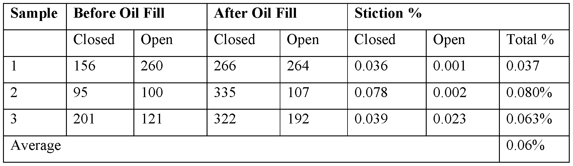

Claims
Priority Applications (3)
| Application Number | Priority Date | Filing Date | Title |
|---|---|---|---|
| JP2017567462A JP2018527198A (en) | 2015-07-02 | 2016-06-02 | Silane control fluid for MEMS stiction reduction |
| KR1020177037869A KR20180023916A (en) | 2015-07-02 | 2016-06-02 | Silane Reforming Fluid for MEMS Static Friction Reduction |
| CN201680035458.8A CN107709224A (en) | 2015-07-02 | 2016-06-02 | The silane-modified fluid reduced for MEMS static friction |
Applications Claiming Priority (2)
| Application Number | Priority Date | Filing Date | Title |
|---|---|---|---|
| US14/790,633 | 2015-07-02 | ||
| US14/790,633 US20170003499A1 (en) | 2015-07-02 | 2015-07-02 | Silane modified fluid for mems stiction reduction |
Publications (2)
| Publication Number | Publication Date |
|---|---|
| WO2017003638A1 true WO2017003638A1 (en) | 2017-01-05 |
| WO2017003638A9 WO2017003638A9 (en) | 2017-04-20 |
Family
ID=56137561
Family Applications (1)
| Application Number | Title | Priority Date | Filing Date |
|---|---|---|---|
| PCT/US2016/035581 Ceased WO2017003638A1 (en) | 2015-07-02 | 2016-06-02 | Silane modified fluid for mems stiction reduction |
Country Status (6)
| Country | Link |
|---|---|
| US (1) | US20170003499A1 (en) |
| JP (1) | JP2018527198A (en) |
| KR (1) | KR20180023916A (en) |
| CN (1) | CN107709224A (en) |
| TW (1) | TW201719244A (en) |
| WO (1) | WO2017003638A1 (en) |
Families Citing this family (1)
| Publication number | Priority date | Publication date | Assignee | Title |
|---|---|---|---|---|
| US11253963B1 (en) | 2020-08-17 | 2022-02-22 | Raytheon Company | Separable component assembly having reduced seal stiction |
Citations (1)
| Publication number | Priority date | Publication date | Assignee | Title |
|---|---|---|---|---|
| EP2530507A1 (en) * | 2011-06-02 | 2012-12-05 | Japan Display East Inc. | Display device and method for manufacturing the same |
Family Cites Families (16)
| Publication number | Priority date | Publication date | Assignee | Title |
|---|---|---|---|---|
| US7256467B2 (en) * | 2002-06-04 | 2007-08-14 | Silecs Oy | Materials and methods for forming hybrid organic-inorganic anti-stiction materials for micro-electromechanical systems |
| US7449355B2 (en) * | 2005-04-27 | 2008-11-11 | Robert Bosch Gmbh | Anti-stiction technique for electromechanical systems and electromechanical device employing same |
| US20080248613A1 (en) * | 2006-09-27 | 2008-10-09 | Dongmin Chen | Method of Forming a Micromechanical Device with Microfluidic Lubricant Channel |
| CN101573792B (en) * | 2006-11-02 | 2012-11-21 | 明锐有限公司 | Preferentially deposited lubricant to prevent anti-stiction in micromechanical systems |
| US8436453B2 (en) * | 2006-12-28 | 2013-05-07 | Texas Instruments Incorporated | Micromechanical device lubrication |
| WO2011097252A2 (en) * | 2010-02-02 | 2011-08-11 | Pixtronix, Inc. | Methods for manufacturing cold seal fluid-filled display apparatus |
| CN102279463B (en) * | 2011-04-18 | 2013-10-23 | 上海丽恒光微电子科技有限公司 | Display device with MEMS light valve and method of forming the same |
| KR20120129256A (en) * | 2011-05-19 | 2012-11-28 | 삼성디스플레이 주식회사 | Display substrate, method of manufacturing the same and display panel having the display substrate |
| JP5856758B2 (en) * | 2011-05-23 | 2016-02-10 | ピクストロニクス,インコーポレイテッド | Display device and manufacturing method thereof |
| JP2012242795A (en) * | 2011-05-24 | 2012-12-10 | Japan Display East Co Ltd | Display device |
| KR20130021104A (en) * | 2011-08-22 | 2013-03-05 | 삼성디스플레이 주식회사 | Display substrate and method of manufacturing the same |
| US9809445B2 (en) * | 2011-08-26 | 2017-11-07 | Qualcomm Incorporated | Electromechanical system structures with ribs having gaps |
| US9323041B2 (en) * | 2011-11-30 | 2016-04-26 | Pixtronix, Inc. | Electromechanical systems display apparatus incorporating charge dissipation surfaces |
| KR20130072847A (en) * | 2011-12-22 | 2013-07-02 | 삼성디스플레이 주식회사 | Display apparatus and fabrication method of the same |
| US9487386B2 (en) * | 2013-01-16 | 2016-11-08 | Infineon Technologies Ag | Comb MEMS device and method of making a comb MEMS device |
| US9134532B2 (en) * | 2013-03-13 | 2015-09-15 | Pixtronix, Inc. | MEMS shutter assemblies for high-resolution displays |
-
2015
- 2015-07-02 US US14/790,633 patent/US20170003499A1/en not_active Abandoned
-
2016
- 2016-06-02 KR KR1020177037869A patent/KR20180023916A/en not_active Withdrawn
- 2016-06-02 JP JP2017567462A patent/JP2018527198A/en active Pending
- 2016-06-02 WO PCT/US2016/035581 patent/WO2017003638A1/en not_active Ceased
- 2016-06-02 CN CN201680035458.8A patent/CN107709224A/en active Pending
- 2016-06-21 TW TW105119463A patent/TW201719244A/en unknown
Patent Citations (1)
| Publication number | Priority date | Publication date | Assignee | Title |
|---|---|---|---|---|
| EP2530507A1 (en) * | 2011-06-02 | 2012-12-05 | Japan Display East Inc. | Display device and method for manufacturing the same |
Also Published As
| Publication number | Publication date |
|---|---|
| JP2018527198A (en) | 2018-09-20 |
| CN107709224A (en) | 2018-02-16 |
| US20170003499A1 (en) | 2017-01-05 |
| KR20180023916A (en) | 2018-03-07 |
| TW201719244A (en) | 2017-06-01 |
| WO2017003638A9 (en) | 2017-04-20 |
Similar Documents
| Publication | Publication Date | Title |
|---|---|---|
| US20140184621A1 (en) | Display apparatus including dual actuation axis electromechanical systems light modulators | |
| US20140184573A1 (en) | Electromechanical Systems Color Transflective Display Apparatus | |
| US20150382465A1 (en) | Systems and methods for implementing display drivers | |
| WO2013081846A1 (en) | Electromechanical systems display apparatus incorporating charge dissipation surfaces | |
| US9196199B2 (en) | Display having staggered display element arrangement | |
| US9223128B2 (en) | Display apparatus with densely packed electromechanical systems display elements | |
| US9030723B2 (en) | Asymmetric travel for MEMS light modulator | |
| US9245311B2 (en) | Display apparatus actuators including anchored and suspended shutter electrodes | |
| US20140375538A1 (en) | Display apparatus incorporating constrained light absorbing layers | |
| US9217857B2 (en) | Multi-state shutter assemblies having segmented drive electrode sets | |
| KR20150100934A (en) | Preventing glass particle injection during the oil fill process | |
| US20170003499A1 (en) | Silane modified fluid for mems stiction reduction | |
| US20150310787A1 (en) | Ems displays incorporating conductive edge seals and methods for manufacturing thereof | |
| US20140175909A1 (en) | Systems and Methods for Supporting a Movable Element of an Electromechanical Device | |
| US20160054482A1 (en) | Display apparatus incorporating edge seals for reducing moisture ingress | |
| US20160054561A1 (en) | Display apparatus incorporating edge seals for reducing moisture ingress | |
| WO2016036480A1 (en) | Aperture plate perimeter routing using encapsulated spacer contact | |
| US20160093070A1 (en) | Spacers of different sizes within seal to limit moisture ingress | |
| WO2016028437A1 (en) | Display apparatus incorporating edge seals for reducing moisture ingress |
Legal Events
| Date | Code | Title | Description |
|---|---|---|---|
| 121 | Ep: the epo has been informed by wipo that ep was designated in this application |
Ref document number: 16730607 Country of ref document: EP Kind code of ref document: A1 |
|
| ENP | Entry into the national phase |
Ref document number: 2017567462 Country of ref document: JP Kind code of ref document: A |
|
| ENP | Entry into the national phase |
Ref document number: 20177037869 Country of ref document: KR Kind code of ref document: A |
|
| NENP | Non-entry into the national phase |
Ref country code: DE |
|
| 122 | Ep: pct application non-entry in european phase |
Ref document number: 16730607 Country of ref document: EP Kind code of ref document: A1 |