WO2016190418A1 - タップ切換器 - Google Patents
タップ切換器 Download PDFInfo
- Publication number
- WO2016190418A1 WO2016190418A1 PCT/JP2016/065750 JP2016065750W WO2016190418A1 WO 2016190418 A1 WO2016190418 A1 WO 2016190418A1 JP 2016065750 W JP2016065750 W JP 2016065750W WO 2016190418 A1 WO2016190418 A1 WO 2016190418A1
- Authority
- WO
- WIPO (PCT)
- Prior art keywords
- switch
- semiconductor switch
- terminal
- semiconductor
- tap
- Prior art date
- Legal status (The legal status is an assumption and is not a legal conclusion. Google has not performed a legal analysis and makes no representation as to the accuracy of the status listed.)
- Ceased
Links
Images







Classifications
-
- H—ELECTRICITY
- H01—ELECTRIC ELEMENTS
- H01F—MAGNETS; INDUCTANCES; TRANSFORMERS; SELECTION OF MATERIALS FOR THEIR MAGNETIC PROPERTIES
- H01F29/00—Variable transformers or inductances not covered by group H01F21/00
- H01F29/02—Variable transformers or inductances not covered by group H01F21/00 with tappings on coil or winding; with provision for rearrangement or interconnection of windings
- H01F29/04—Variable transformers or inductances not covered by group H01F21/00 with tappings on coil or winding; with provision for rearrangement or interconnection of windings having provision for tap-changing without interrupting the load current
Definitions
- the embodiment of the present invention relates to a tap changer using a semiconductor switch.
- the tap changer has a current switching element, and switches the tap of the static induction device to uninterruptible.
- a current switching element of the tap changer an oil contact called an arc contact or a vacuum valve can be used.
- an in-oil contact discharge occurs at the contact when the tap is switched, and the surrounding insulating medium may be soiled. Therefore, inspection at a relatively short interval is required. Therefore, in recent years, tap changers that perform switching using a vacuum valve have been put into practical use.
- the tap changer using a vacuum valve has a first vacuum valve and a mechanical contact connected in series to the first vacuum valve, and two auxiliary electric circuits are connected to the first vacuum valve.
- each of the auxiliary electric circuits is provided with a second vacuum valve or a third vacuum valve and a current limiting resistor connected in series to the second and third vacuum valves.
- the vacuum valve is provided with a mechanical contact in a vacuum container, and is opened and closed by a force from a storage mechanism provided outside.
- the embodiment of the present invention has been proposed in order to solve the problems of the prior art as described above.
- the object is to provide a small tap changer with a long maintenance interval.
- a tap changer includes a first terminal and a second terminal connected to a tap winding of a static induction electric device, the first terminal, and the static induction.
- a first semiconductor switch connected between a neutral point terminal of the electric appliance; a second semiconductor switch connected between the second terminal; and the neutral point terminal;
- a third semiconductor switch connected in parallel with the second semiconductor switch, the third semiconductor switch, and the neutral point terminal between the second terminal and the neutral point terminal;
- a resistor connected between the two.
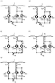
- the tap changer of a 1st embodiment it is a circuit diagram explaining the current which flows through a circuit, when changing from terminal T1 to terminal T2.
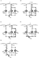
- the tap changer of a 1st embodiment it is a circuit diagram explaining the current which flows through a circuit, when changing from terminal T2 to terminal T1.
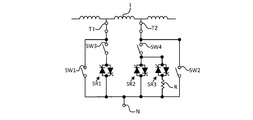
- FIG. 1 is a circuit diagram showing an example of the configuration of the tap changer of the present embodiment.
- FIG. 1 shows a connection portion between a tap winding 1 of a static induction appliance and a neutral point terminal N.
- the tap changer is connected to the tap winding 1 of the static induction appliance via terminals T1 and T2.
- a semiconductor switch SR1 is connected between the terminal T1 and the neutral point terminal N.
- a semiconductor switch SR2 is connected between the terminal T2 and the neutral point terminal N.
- a semiconductor switch SR3 is connected between the terminal T2 and the neutral point terminal N so as to be in parallel with the semiconductor switch SR2.
- a resistor R is connected between the semiconductor switch SR3 and the neutral point terminal N. The neutral point terminal N side of the semiconductor switch SR1, the semiconductor switch SR2, and the resistor R and the neutral point terminal N are connected to each other.
- bidirectional thyristors in which a plurality of thyristors are connected in antiparallel can be used.
- bidirectional current can flow.
- FIG. 1 shows an example in which two thyristors are connected in antiparallel
- the number of thyristors to be used can be designed as appropriate.
- the withstand voltage may be improved by connecting two or more bidirectional thyristors in series.
- a self-excited switching element such as GTO or IGBT may be used as the semiconductor switch.
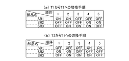
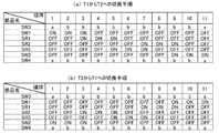
- FIG. 2A is a table showing a switching sequence when switching from the terminal T1 to T2.
- FIG. 3 is a circuit diagram illustrating a current when switching from terminal T1 to T2.
- the closed state of the switch is indicated as ON, and the open state is indicated as OFF.
- the timing when the switch is turned off is the timing when the current of the tap winding 1 becomes 0 A when a thyristor is used for the semiconductor switch.
- the timing for turning off the switch can be arbitrarily determined, but the timing at which the current of the winding 1 becomes 0 A is desirable from the viewpoint of preventing the occurrence of a surge.
- the semiconductor switch SR1 is in the ON state while the semiconductor switches SR2 and SR3 are in the OFF state, as shown in order 1 of FIG. 2 (a).
- the current flows from the tap winding 1 to the neutral point terminal N through the terminal T1 and the semiconductor switch SR1.
- the semiconductor switch SR3 is turned on while maintaining the ON state of the semiconductor switch SR1. Then, as shown in FIG. 3B, the current flows from the tap winding 1 to the neutral point terminal N via the terminal T1 and the semiconductor switch SR1, and from the tap winding 1 to the terminal T2, the semiconductor switch.
- the current is shunted to the current flowing through the neutral point terminal N via SR3 and the resistor R.
- the presence of the resistor R can significantly suppress the circulating current that flows to the terminal T2 via the terminal T1, the semiconductor switch SR1, and the semiconductor switch SR3.
- the semiconductor switch SR1 is turned OFF.
- current flows from the tap winding 1 to the neutral point terminal N via the terminal T 2, the semiconductor switch SR 3, and the resistor R.
- the semiconductor switch SR2 is turned on. Since the resistor R is connected to the semiconductor switch SR3, as shown in FIG. 3 (4), most of the current flows from the tap winding 1 through the terminal T2 and the semiconductor switch SR2 to the neutral point terminal N. Flowing into. However, there is also a current that flows from the tap winding 1 to the neutral point terminal N via the terminal T2, the semiconductor switch SR3, and the resistor R.
- the semiconductor switch SR3 is turned OFF. Then, as shown in FIG. 3 (5), the current is only the current flowing from the tap winding 1 to the neutral point terminal N via the terminal T2 and the semiconductor switch SR2. As described above, the switching sequence is completed, and the operation is continued in the state shown in FIG.
- FIG. 2B is a table showing a switching sequence when switching from the terminal T2 to T1.
- FIG. 4 is a circuit diagram illustrating the current when switching from the terminal T2 to T1.
- the semiconductor switch SR2 is in the ON state, while the semiconductor switches SR1 and SR3 are in the OFF state, as shown in order 1 of FIG. 2 (b).
- the current flows from the tap winding 1 to the neutral point terminal N through the terminal T2 and the semiconductor switch SR2.
- the semiconductor switch SR3 is turned on while the semiconductor switch SR2 is kept on. Then, as shown in FIG. 4 (2), the current flows from the tap winding 1 to the neutral point terminal N via the terminal T2 and the semiconductor switch SR2, and from the tap winding 1 to the terminal T2, the semiconductor switch.
- the current flowing through the neutral point terminal N via the SR3 and the resistor R is divided in accordance with the resistance ratio.
- the semiconductor switch SR2 is turned OFF.
- current flows from the tap winding 1 to the neutral point terminal N via the terminal T 2, the semiconductor switch SR 3, and the resistor R.
- the semiconductor switch SR1 is turned on. Since the resistor R is connected to the semiconductor switch SR3, as shown in FIG. 4 (4), most of the current flows from the tap winding 1 through the terminal T1 and the semiconductor switch SR1 to the neutral point terminal N. Flowing into. However, there is also a current that flows from the tap winding 1 to the neutral point terminal N via the terminal T2, the semiconductor switch SR3, and the resistor R.
- the semiconductor switch SR3 is turned OFF.
- the current is only the current flowing from the tap winding 1 to the neutral point terminal N via the terminal T1 and the semiconductor switch SR1.
- the switching sequence is completed, and the operation is continued in the state shown in FIG.
- the third switch The switching can be performed by turning on the semiconductor switch SR3, turning off the connection switch, turning on the other semiconductor switch, and turning off the third semiconductor SR3 switch.
- the semiconductor switches SR1, SR2, SR3 do not require an energy storage mechanism, and the total number of switches constituting the tap changer is as small as three, so that the tap changer can be downsized.
- the contact in oil can contaminate the insulating medium by arc discharge.
- the semiconductor switches SR1, SR2, and SR3 switching can be performed regardless of the number of switching times and the switching speed. That is, since the switch does not deteriorate due to switching, no mechanical adjustment is required. Further, since there is no mechanism for generating arc discharge, the insulating medium is not contaminated by discharge. Therefore, the interval between inspection and replacement of parts can be made longer than before. As described above, it is possible to provide a tap changer that is small and has a long maintenance interval.
- this embodiment has semiconductor switches SR1, SR2, SR3. Since the vacuum valve is not used, there is no limitation due to the pressure difference between the vacuum valve and the surrounding insulating medium, and the limitation of the insulating medium to be used can be relaxed as compared with the conventional case.
- the switching sequence as described above makes it possible to switch taps using only the three semiconductor switches SR1, SR2, and SR3.
- it is not necessary to provide four or more semiconductor switches or use other mechanical contacts it is possible to provide a tap changer that is small and has a long maintenance interval.
- the configuration of the tap changer according to the modification of the first embodiment is basically the same as that of the first embodiment.
- the semiconductor switch SR3 is turned on immediately before the current of the tap winding 1 becomes 0A, and the connection switch is turned off when the current of the tap winding 1 becomes 0A.
- the other semiconductor switch is turned on immediately after the connection switch is turned off.
- the current of the tap winding 1 becomes 0 A, it can be obtained from a current waveform that changes periodically. For example, in the case of drawing a waveform in which the current value increases and then decreases after the current has once decreased to 0 A, the time when the current value becomes 1 A in the current waveform that tends to decrease can be immediately before 0 A. . Similarly, when drawing a waveform that rises after the current value decreases after the current has once reached 0A, the current value that is ⁇ 1A in the current waveform that tends to rise is immediately before it reaches 0A. Can do. What is necessary is just to measure the current waveform of the tap winding 1 with a current measuring instrument.
- the semiconductor switch SR3 when switching from the terminal T1 to the terminal T2, the semiconductor switch SR3 is turned ON immediately before the current of the tap winding 1 becomes 0A in the state where the semiconductor switch SR1 is ON (sequence 1). (Order 2). Then, at the subsequent current zero point, the semiconductor switch SR1 is turned OFF (order 3). Thereafter, the semiconductor switch SR2 is immediately turned ON (order 4). The semiconductor switch SR3 is turned off at the current zero point after the semiconductor switch SR2 is turned on (sequence 5).
- the following operational effects can be obtained in addition to the above-described embodiment. That is, by turning on the semiconductor switch SR3 immediately before the winding current becomes 0A, when the current subsequently becomes 0A, the connection switch can be turned off, and the other semiconductor switches can be turned on quickly.
- the other semiconductor switch is turned on, the current mainly flows on the other semiconductor switch side without the resistor R. Therefore, the time during which current flows through the semiconductor switch SR3 and the resistor R can be shortened. Therefore, the heat capacities of the semiconductor switch SR3 and the resistor R can be minimized.
- the resistor R Since the resistor R generates heat when a current flows, it is necessary to increase the resistance when the current flows through the resistor R for a long time. However, in the modified example of the present embodiment, the time during which current flows through the resistor R is shortened, so that the resistor R can be downsized.
- the configuration of the tap changer of the second embodiment is basically the same as that of the first embodiment.
- the switch SW1 is connected in parallel with the semiconductor switch SR1.
- the switch SW2 is connected in parallel with the semiconductor switches SR2 and SR3.
- the switches SW1 and SW2 are mechanical switches that are driven by external power.
- FIG. 6A is a table showing a switching sequence when switching from the terminal T1 to T2.
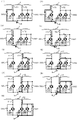
- FIG. 7 is a circuit diagram illustrating a current when switching from the terminal T1 to T2.
- the switch SW1 is in the ON state, while the semiconductor switches SR1 to SR3 and the switch SW2 are in the OFF state.
- the current flows from the tap winding 1 to the neutral point terminal N via the terminal T1 and the switch SW1.
- the semiconductor switch SR1 is turned on while maintaining the ON state of the switch SW1. Then, as shown in FIG. 7B, the current flows from the tap winding 1 to the neutral point terminal N via the terminal T1 and the switch SW1, and from the tap winding 1 to the terminal T1 and the semiconductor switch SR1. To the current flowing through the neutral point terminal N.
- the switch SW2 is turned on while the semiconductor switch SR2 is kept on.
- the current flows from the tap winding 1 to the neutral point terminal N via the terminal T2 and the switch SW2, and from the tap winding 1 to the terminal T2 and the semiconductor switch SR2. To the current flowing through the neutral point terminal N.
- the semiconductor switch SR2 is turned OFF.
- the current is only the current that flows from the tap winding 1 to the neutral point terminal N via the terminal T2 and the switch SW2. As described above, the switching sequence is completed, and the operation is continued in the state shown in FIG.
- FIG. 6B is a table showing a switching sequence when switching from the terminal T2 to T1.
- FIG. 8 is a circuit diagram illustrating the current when switching from the terminal T2 to T1.
- the switch SW2 is in the ON state, while the semiconductor switches SR1 to SR3 and the switch SW1 are in the OFF state.
- the current flows from the tap winding 1 to the neutral point terminal N through the terminal T2 and the switch SW2.
- the semiconductor switch SR2 is turned on while maintaining the ON state of the switch SW2. Then, as shown in FIG. 8 (2), the current flows from the tap winding 1 to the neutral point terminal N via the terminal T2 and the switch SW2, and from the tap winding 1 to the terminal T2 and the semiconductor switch SR2. To the current flowing through the neutral point terminal N.
- the switch SW1 is turned on while the semiconductor switch SR1 is kept on. Then, as shown in FIG. 8 (8), the current flows from the tap winding 1 to the neutral point terminal N via the terminal T1 and the switch SW1, and from the tap winding 1 to the terminal T1 and the semiconductor switch SR1. To the current flowing through the neutral point terminal N.
- the semiconductor switch SR1 is turned OFF.
- the current is only the current that flows from the tap winding 1 to the neutral point terminal N via the terminal T2 and the switch SW1. As described above, the switching sequence is completed, and the operation is continued in the state shown in FIG.
- either the switch SW1 or the switch SW2 is a connection switch connected to the tap winding 1, and when switching to the other switch, the semiconductor switch SR1 connected in parallel with the connection switch.
- the semiconductor switch SR2 is turned on, the connection switch is turned off, the semiconductor switch SR3 is turned on, the semiconductor switch SR1 or the semiconductor switch SR2 connected in parallel with the connection switch is turned off, and the other switch is connected in parallel.
- the semiconductor switch SR1 or the semiconductor switch SR2 is turned ON, the semiconductor switch SR1 is turned OFF, the other switch is turned ON, and the semiconductor switch SR1 or the semiconductor switch SR2 connected in parallel with the other switch is turned OFF, Can be switched Kill.
- the switches SW1 and SW2 which are mechanical switches are used during the steady operation, and thus no resistance is generated in the circuit during the steady operation.
- the semiconductor switches SR1 and SR2 are not energized, the heat capacities of the semiconductor switches SR1 and SR2 can be minimized.
- Either the switch SW1 or the switch SW2 is a connection switch connected to the tap winding 1, and when switching to the other switch, the semiconductor switch SR1 connected in parallel with the connection switch or Semiconductor switch SR2 is turned on, connection switch is turned off, semiconductor switch SR3 is turned on, semiconductor switch SR1 or semiconductor switch SR2 connected in parallel with the connection switch is turned off, and the other switch is connected in parallel.
- the semiconductor switch SR1 or the semiconductor switch SR2 is turned on, the semiconductor switch SR1 is turned off, the other switch is turned on, and the semiconductor switch SR1 or the semiconductor switch SR2 connected in parallel with the other switch is turned off.
- the current flows through the switch SW1 or SW2 during steady operation, and the semiconductor switches SR1 to SR3 are used only when the switching operation is performed. Therefore, the switches SW1 and SW2 only need to cut the voltage corresponding to the internal resistance of the semiconductor switches SR1 to SR3. Therefore, a simple mechanical switch can be used instead of a shut-off device such as a vacuum valve or a switch gear. That is, the switches SW1 and SW2 do not require a large driving force when being contacted or released. Therefore, even if the mechanical switch and its operation mechanism are taken into consideration, a tap changer that is smaller than the conventional one can be provided.
- the switches SW1 and SW2 may be cut off the voltage corresponding to the internal resistance of the semiconductor switches SR1 to SR3. Therefore, a large arc discharge that contaminates the surrounding insulating medium does not occur. As described above, it is possible to provide a tap changer that is small and has a long maintenance interval.
- the semiconductor switch is vulnerable to overvoltage, in this embodiment, current flows through the switches SW1 and SW2 during steady operation. Therefore, even if an overvoltage enters the circuit, it flows through the switches SW1 and SW2. From the above, it is possible to prevent an overvoltage from being applied to both sides of the semiconductor switch.
- the configuration of the tap changer according to the modification of the second embodiment is basically the same as that of the second embodiment. However, in the tap changer of the present embodiment, it is assumed that a plurality of taps are switched, and before performing a series of switching operations, the switches SW1 and SW2 are turned off and the semiconductor switches SR1 to SR3 continuously. Perform switching operation.
- steps 3 to 7 in FIGS. 6A and 6B are repeated continuously and a predetermined number of times with the switches SW1 and SW2 turned OFF.
- a tap selector (not shown) connected to the tap changer selects a tap to be operated from the tap winding of the static induction device.
- the tap changer switches the circuit to the tap selected by the tap selector.
- the tap changer of the modified example performs an operation of switching to the next tap selected by the tap selector without switching the switches SW1 and SW2 after switching the circuit.
- This tap switching operation is performed a plurality of times, and when a series of switching operations are completed, the switch SW1 or SW2 is turned ON, and the semiconductor switch SR1 or the semiconductor switch SR2 connected in parallel with the ON switch is turned OFF. The switching operation is completed.
- the tap changer is a connection switch in which either the switch SW1 or the switch SW2 is connected to the tap winding 1 and switches the plurality of taps continuously.
- the semiconductor switch SR1 or the semiconductor switch SR2 connected in parallel with the connection switch is turned on, the switch SW1 and the switch SW2 are turned off, and the semiconductor switch SR3 is turned on before starting a series of switching operations.
- the semiconductor switch SR1 or semiconductor switch SR2 connected in parallel with the connection switch is turned OFF, the semiconductor switch SR1 or semiconductor switch SR2 connected in parallel with the other switch is turned ON, and the semiconductor switch SR3 is turned OFF. Repeated a predetermined number of times, a series of switching After operation completion, the switch SW1 or switch SW2 and ON, the turned OFF the semiconductor switch SR1 or semiconductor switches SR2 are connected in parallel with the other switch.
- the tap can be switched continuously and at high speed. As described above, it is possible to obtain a tap changer using a semiconductor switch that can continuously switch taps at a higher speed than a tap changer using a conventional contact in oil or a vacuum valve.
- the configuration of the tap changer of the third embodiment is basically the same as that of the second embodiment.
- the switch SW3 is connected in series with the semiconductor switch SR1 on the terminal T1 side of the semiconductor switch SR1.
- the switch SW4 is connected to the terminal T2 side of the semiconductor switch SR2 so as to be in series with the semiconductor switch SR2.
- the switches SW3 and SW4 are mechanical switches that are driven by external power.
- the switch SW3 is provided between the semiconductor switch SR1 and the contact on the terminal T1 side of the switch SW1 and the semiconductor switch SR1. That is, the semiconductor switch SR1 is disconnected from the circuit when the switch SW3 is turned off.
- the switch SW4 is provided between the contact on the terminal T2 side of the semiconductor switch SR2 and the switch SW2 and the contact on the terminal T2 side of the semiconductor switch SR2 and the semiconductor switch SR3. That is, when the switch SW4 is turned off, the semiconductor switches SR2 and SR3 are disconnected from the circuit.
- FIG. 10A is a table showing a switching sequence when switching from the terminal T1 to T2
- FIG. 10B is a table showing a switching sequence when switching from the terminal T2 to T1.
- the switch SW1 is in the ON state, while the semiconductor switches SR1 to SR3 and the switches SW2 to 4 are in the OFF state. Current flows from the tap winding 1 to the neutral point terminal N via the terminal T1 and the switch SW1.
- Orders 3 to 10 in FIG. 10A are the same sequences as orders 3 to 10 in FIG.
- the semiconductor switch SR2 is turned OFF, and the current is only the current flowing from the tap winding 1 to the neutral point terminal N via the terminal T2 and the switch SW2.
- the switches SW3 and SW4 are turned on in order 2 of FIG. 10B, and the semiconductor switches SR1 to SR3 are connected to the circuit. Further, in order 11 of FIG. 10B, the switches SW3 and SW4 are turned OFF, and the semiconductor switches SR1 to SR3 are disconnected from the circuit.
- the order 3 to 10 in FIG. 10B is the same sequence as the order 3 to 10 in FIG.
- the switch SW3 and the switch SW4 are turned on before the switching operation is started, and the switch SW3 and the switch SW4 are turned off after the switching operation is completed.
- the semiconductor switches SR1 to SR3 may be damaged due to overcurrent / overvoltage, they can be disconnected from the main circuit by the switches SW3 and SW4 during steady operation, so that the semiconductor switches SR1 to SR3 are damaged by lightning strikes, etc. Can be prevented. That is, the failure probability of the semiconductor switches SR1 to SR3 due to an external surge or abnormal current can be reduced, and long-term reliability can be improved. This makes it possible to further increase the interval between inspection and replacement.
- the configuration of the tap changer according to the modification of the third embodiment is basically the same as that of the third embodiment.
- the switches SW3 and SW4 are turned on and the semiconductor switches SR1 to SR3 are connected to the circuit before a series of switching operations.
- steps 3 to 9 in FIGS. 10A and 10B are executed continuously and repeatedly with the switches SW3 and SW4 turned on.
- a tap selector (not shown) connected to the tap changer selects a tap to be operated from the tap winding of the static induction device.
- the tap changer switches the circuit to the tap selected by the tap selector.
- the tap changer of the modified example performs an operation of switching to the next tap selected by the tap selector without switching the switches SW3 and SW4 after switching the circuit. This tap switching operation is performed a plurality of times, and when a series of switching operations are completed, the switches SW3 and SW4 are turned OFF, and the semiconductor switches SR1 to SR3 are disconnected from the circuit.
- the tap changer switches a plurality of taps continuously.
- the switch SW3 and the switch SW4 are turned on before starting a series of switching operations, and the switch SW3 and the switch SW4 are turned off after the series of switching operations are completed. .
- the tap can be switched continuously and at high speed. As described above, it is possible to obtain a tap changer using a semiconductor switch that can continuously switch taps at a higher speed than a tap changer using a conventional contact in oil or a vacuum valve.
- the configuration of the tap changer of the fourth embodiment is basically the same as that of the third embodiment. However, in the tap changer of the present embodiment, as shown in FIG. 11, the switch SW3 and the switch SW4 are configured by a three-point switch.
- the switch SW3 has a contact point a that grounds the semiconductor switch SR1, and a contact point b that connects the terminal T1 and the semiconductor switch SR1.
- the switch SW3 is in the OFF state, that is, when the switch SW3 is connected to the contact a, the semiconductor switch SR1 is short-circuited at both ends.
- the switch SW3 is in the ON state, that is, when the switch SW3 is connected to the contact b, the semiconductor switch SR1 is connected to the terminal T1.
- the switch SW4 has a contact point a that grounds the semiconductor switch SR2 and the semiconductor switch SR3, and a contact point b that connects the terminal T2 and the semiconductor switch SR2 and the semiconductor switch SR3.
- the switch SW4 is in an OFF state, that is, when the switch SW4 is connected to the contact a, the semiconductor switch SR2 and the semiconductor switch SR3 are short-circuited at both ends.
- the switch SW4 is in the ON state, that is, when the switch SW4 is connected to the contact b, the semiconductor switch SR2 and the semiconductor switch SR3 are connected to the terminal T1.
- FIG. 12A is a table showing a switching sequence when switching from the terminal T1 to T2
- FIG. 12B is a table showing a switching sequence when switching from the terminal T2 to T1.
- the switch SW1 is in the ON state, while the semiconductor switches SR1 to SR3 and the switch SW2 are in the OFF state. Further, the switch SW3 and the switch SW4 are connected to the contact a, and the semiconductor switch SR1 is in a state where both ends thereof are short-circuited. Current flows from the tap winding 1 to the neutral point terminal N via the terminal T1 and the switch SW1.
- the switches SW3 and SW4 are connected to the contact b while maintaining the ON state of the switch SW1, and the semiconductor switches SR1 to SR3 are connected to the circuit.
- Orders 3 to 10 in FIG. 12A are the same sequences as orders 3 to 10 in FIG.
- the semiconductor switch SR2 is turned OFF, and the current is only the current flowing from the tap winding 1 to the neutral point terminal N via the terminal T2 and the switch SW2.
- the switches SW3 and SW4 are connected to the contact b, and the semiconductor switches SR1 to SR3 are connected to the circuit. Further, in order 11 of FIG. 12B, the switches SW3 and SW4 are connected to the contact a. Then, the semiconductor switches SR1 to SR3 are disconnected from the circuit and both ends thereof are short-circuited.
- the order 3 to 10 in FIG. 10B is the same sequence as the order 3 to 10 in FIG.
- the switch SW3 and the switch SW4 are three-point switches, and the switch SW3 has a contact a that grounds the semiconductor switch SR1 and a contact b that connects the terminal T1 and the semiconductor switch SR1, and the switch SW4 is a semiconductor switch
- the contact a for grounding the switch SR2 and the semiconductor switch SR3 and the contact b for connecting the terminal T2 to the semiconductor switch SR2 and the semiconductor switch SR3 are provided.
- the semiconductor switches SR1 to SR3 can be disconnected from the main circuit and both ends thereof can be short-circuited.
- the configuration of the tap changer of the fifth embodiment is basically the same as that of the fourth embodiment.
- the voltage suppression element 2 is connected in parallel to the semiconductor switches SR1 to SR3.
- an element that conducts when a certain voltage or more is applied such as a nonlinear element arrester, can be used.
- the voltage suppression element 2 has a function of protecting the semiconductor from overvoltage.
- the following effects can be obtained in addition to the above embodiment. Even when an abnormal voltage is generated due to an external surge or the like while the semiconductor switches SR1 to SR3 are energized during the switching operation, the semiconductor switches SR1 to SR3 can be prevented from being destroyed. Therefore, long-term reliability is improved, and the interval between inspection and replacement can be further increased.
- the contacts of the semiconductor switches SR1 to SR3 and the switches SW1 to SW4 are opened and closed by a computer including a CPU and a memory that operates according to a predetermined program and a dedicated electronic circuit (not shown) This is done by the control device.
- the control device detects the state of the tap changer or tap selector and automatically opens and closes the contacts.
- the control device can be manually operated by the operator via the control device.
- said embodiment can also be grasped
Landscapes
- Engineering & Computer Science (AREA)
- Power Engineering (AREA)
- Driving Mechanisms And Operating Circuits Of Arc-Extinguishing High-Tension Switches (AREA)
Abstract
小型でメンテンナンス間隔を長期化させたタップ切換器を提供する。静止誘導電器のタップ巻線1に接続される第1の端子T1および第2の端子T2と、第1の端子T1と、静止誘導電器の中性点端子Nと、の間に接続された第1の半導体スイッチSR1と、第2の端子T2と、中性点端子Nと、の間に接続された第2の半導体スイッチSR2と、第2の端子T2と、中性点端子Nと、の間に、第2の半導体スイッチSR2と並列に接続された第3の半導体スイッチSR3と、第3の半導体スイッチSR3と、中性点端子Nと、の間に接続された抵抗器Rと、を有する。
Description
本発明の実施形態は、半導体スイッチを用いたタップ切換器に関する。
タップ切換器は、電流開閉素子を有し、静止誘導電器のタップを無停電に切換える。タップ切換器の電流開閉素子としては、アーク接点とよばれる油中接点や、真空バルブが用いることができる。ただし、油中接点を使用したタップ切換器では、タップの切換時に接点で放電が発生し、周囲の絶縁媒体を汚損することがある。そのため、比較的短い間隔での点検を要する。従って、近年では、真空バルブを使用して切換を行うタップ切換器が実用化されている。
真空バルブを用いたタップ切換器としては、第1の真空バルブと、第1の真空バルブに対して直列に接続された機械式接触子とを有し、第1の真空バルブに2つの補助電路を設け、補助電路のそれぞれに、第2の真空バルブ又は第3の真空バルブと、第2および第3の真空バルブに対して直列に接続された限流抵抗を設ける構成が提案されている。真空バルブは、真空の容器内に機械式接点が設けられており、外部に設けられた蓄勢機構からの力により開閉される。
しかしながら、真空バルブのような機械式接点を設けた場合、切換可能回数の最大値が設定されており、切換回数に応じたメンテナンスが随時必要となる。特に切換回数が多い接点では、真空バルブの劣化が生じる。また、接点を動作させるための蓄勢機構によりタップ切換器が大型化する問題があった。
また、真空バルブを用いた場合、絶縁媒体として高圧ガスを用いることができない。すなわち、絶縁耐性を上げるためにガスを圧縮すると、真空バルブがその圧力に耐えられなくなる。そのため、真空バルブにガスを用いる場合には、ガス圧を下げることになるが、ガス圧を下げると絶縁耐力が低くなり、絶縁耐力を持たせるためにタップ切換器を大型化する必要が生じていた。
本発明の実施形態は、上記のような従来技術の問題点を解決するために提案されたものである。その目的は、小型でメンテンナンス間隔を長期化させたタップ切換器を提供することである。
上記のような目的を達成するための実施形態のタップ切換器は、静止誘導電器のタップ巻線に接続される第1の端子および第2の端子と、前記第1の端子と、前記静止誘導電器の中性点端子と、の間に接続された第1の半導体スイッチと、前記第2の端子と、前記中性点端子と、の間に接続された第2の半導体スイッチと、前記第2の端子と、前記中性点端子と、の間に、前記第2の半導体スイッチと並列に接続された第3の半導体スイッチと、前記第3の半導体スイッチと、前記中性点端子と、の間に接続された抵抗器と、を有することを特徴とする。
[第1の実施形態]
[1.構成]
以下、本発明の第1の実施形態について、図面を参照して説明する。図1は、本実施形態のタップ切換器の構成の一例を示す回路図である。図1は、静止誘導電器のタップ巻線1と、中性点端子Nとの接続部を示している。タップ切換器は、静止誘導電器のタップ巻線1に、端子T1およびT2を介して接続されている。
[1.構成]
以下、本発明の第1の実施形態について、図面を参照して説明する。図1は、本実施形態のタップ切換器の構成の一例を示す回路図である。図1は、静止誘導電器のタップ巻線1と、中性点端子Nとの接続部を示している。タップ切換器は、静止誘導電器のタップ巻線1に、端子T1およびT2を介して接続されている。
端子T1と中性点端子Nとの間には、半導体スイッチSR1が接続されている。端子T2と中性点端子Nとの間には、半導体スイッチSR2が接続されている。また、端子T2と中性点端子Nとの間には、半導体スイッチSR3が、半導体スイッチSR2と並列となるように接続されている。半導体スイッチSR3と中性点端子Nとの間には、抵抗器Rが接続されている。半導体スイッチSR1、半導体スイッチSR2、および抵抗器Rの中性点端子N側と、中性点端子Nとは、互いに接続されている。
半導体スイッチSR1、SR2、SR3としては、複数のサイリスタを逆並列に接続した双方向サイリスタを用いることができる。双方向サイリスタでは、双方向の電流を流すことができる。図1では、2個のサイリスタを逆並列に接続した例を示しているが、用いるサイリスタの数は適宜設計可能である。また、例えば双方向サイリスタを多直列に接続して、耐圧を向上させても良い。半導体スイッチとしては、他にも、GTOやIGBT等の自励式のスイッチング素子を用いても良い。
[2.切換シーケンス]
本実施形態のタップ切換器の切換シーケンスについて、図2~4を参照して説明する。
本実施形態のタップ切換器の切換シーケンスについて、図2~4を参照して説明する。
(端子T1からT2へ切換える場合)
図2(a)は、端子T1からT2に切換える際の切換シーケンスを示す表である。図3は、端子T1からT2に切換える際の電流を説明する回路図である。なお、以下では、スイッチを閉じている状態をON、開いている場合をOFFと示して説明する。また、スイッチをOFFとするタイミングは、半導体スイッチにサイリスタを用いた場合は、タップ巻線1の電流が0Aとなるタイミングである。半導体スイッチに自励式のスイッチング素子を用いた場合、スイッチをOFFするタイミングは任意に決めることができるが、サージの発生を防ぐ観点から、巻線1の電流が0Aとなるタイミングが望ましい。
図2(a)は、端子T1からT2に切換える際の切換シーケンスを示す表である。図3は、端子T1からT2に切換える際の電流を説明する回路図である。なお、以下では、スイッチを閉じている状態をON、開いている場合をOFFと示して説明する。また、スイッチをOFFとするタイミングは、半導体スイッチにサイリスタを用いた場合は、タップ巻線1の電流が0Aとなるタイミングである。半導体スイッチに自励式のスイッチング素子を用いた場合、スイッチをOFFするタイミングは任意に決めることができるが、サージの発生を防ぐ観点から、巻線1の電流が0Aとなるタイミングが望ましい。
まず、端子T1が接続されている場合、図2(a)の順序1に示す通り、半導体スイッチSR1はON状態である一方、半導体スイッチSR2およびSR3はOFF状態である。図3(1)に示す通り、電流は、タップ巻線1から、端子T1および半導体スイッチSR1を介して中性点端子Nに流れる。
ここで、端子T1から端子T2に切換える場合、端子T1と端子T2を同時にON状態とすると、電流は中性点端子Nに流れず、端子T1側から、タップ切換器内の回路を通し端子T2側に流れる循環電流となり、温度上昇による巻線の焼損や、電磁機械力による巻線の変形が発生する恐れがある。そこで、図2(a)の順序2に示す通り、半導体スイッチSR1のON状態を維持したままで、半導体スイッチSR3をONする。すると、図3(2)に示す通り、電流は、タップ巻線1から、端子T1および半導体スイッチSR1を介して中性点端子Nに流れる電流と、タップ巻線1から、端子T2、半導体スイッチSR3、および抵抗器Rを介して中性点端子Nに流れる電流に分流する。また、抵抗Rがあることで、端子T1、半導体スイッチSR1、半導体スイッチSR3を介して端子T2に流れる循環電流を大幅に抑制することができる。
次に、図2(a)の順序3に示す通り、半導体スイッチSR1をOFFする。すると、図3(3)に示す通り、電流は、タップ巻線1から、端子T2、半導体スイッチSR3、および抵抗器Rを介して中性点端子Nに流れる。そして、図2(a)の順序4に示す通り、半導体スイッチSR2をONする。半導体スイッチSR3には抵抗器Rが接続されているため、図3(4)に示す通り、電流の大部分は、タップ巻線1から、端子T2および半導体スイッチSR2を介して中性点端子Nに流れる。ただし、タップ巻線1から、端子T2、半導体スイッチSR3、および抵抗器Rを介して中性点端子Nに流れる電流も存在する。
最後に、図2(a)の順序5に示す通り、半導体スイッチSR3をOFFにする。すると、図3(5)に示す通り、電流は、タップ巻線1から、端子T2および半導体スイッチSR2を介して中性点端子Nに流れる電流のみとなる。以上のように切換シーケンスを終了し、図3(5)に示す状態で運転を継続することとなる。
(端子T2からT1へ切換える場合)
図2(b)は、端子T2からT1に切換える際の切換シーケンスを示す表である。図4は、端子T2からT1に切換える際の電流を説明する回路図である。
図2(b)は、端子T2からT1に切換える際の切換シーケンスを示す表である。図4は、端子T2からT1に切換える際の電流を説明する回路図である。
まず、端子T2が接続されている場合、図2(b)の順序1に示す通り、半導体スイッチSR2はON状態である一方、半導体スイッチSR1およびSR3はOFF状態である。図4(1)に示す通り、電流は、タップ巻線1から、端子T2および半導体スイッチSR2を介して中性点端子Nに流れる。
ここで、図2(b)の順序2に示す通り、半導体スイッチSR2のON状態を維持したままで、半導体スイッチSR3をONする。すると、図4(2)に示す通り、電流は、タップ巻線1から、端子T2および半導体スイッチSR2を介して中性点端子Nに流れる電流と、タップ巻線1から、端子T2、半導体スイッチSR3、および抵抗器Rを介して中性点端子Nに流れる電流に抵抗比に見合って分流する。
次に、図2(b)の順序3に示す通り、半導体スイッチSR2をOFFする。すると、図4(3)に示す通り、電流は、タップ巻線1から、端子T2、半導体スイッチSR3、および抵抗器Rを介して中性点端子Nに流れる。そして、図2(b)の順序4に示す通り、半導体スイッチSR1をONする。半導体スイッチSR3には抵抗器Rが接続されているため、図4(4)に示す通り、電流の大部分は、タップ巻線1から、端子T1および半導体スイッチSR1を介して中性点端子Nに流れる。ただし、タップ巻線1から、端子T2、半導体スイッチSR3、および抵抗器Rを介して中性点端子Nに流れる電流も存在する。
最後に、図2(b)の順序5に示す通り、半導体スイッチSR3をOFFにする。すると、図4(5)に示す通り、電流は、タップ巻線1から、端子T1および半導体スイッチSR1を介して中性点端子Nに流れる電流のみとなる。以上のように切換シーケンスを終了し、図4(5)に示す状態で運転を継続することとなる。
以上の通り、第1の半導体スイッチSR1または第2の半導体スイッチSR2のいずれかがタップ巻線1に接続されている接続スイッチであり、他方の半導体スイッチへの切換えを行う場合には、第3の半導体スイッチSR3をONとし、接続スイッチをOFFとし、他方の半導体スイッチをONとし、第3の半導体SR3スイッチをOFFとすることで、切換えを行うことができる。
[3.作用効果]
以上のような本実施形態の作用効果は以下のとおりである。
(1)静止誘導電器のタップ巻線1に接続される端子T1および端子T2と、端子T1と、静止誘導電器の中性点端子Nと、の間に接続された半導体スイッチSR1と、端子T2と、中性点端子Nと、の間に接続された半導体スイッチSR2と、端子T2と、中性点端子Nと、の間に、半導体スイッチSR2と並列に接続された半導体スイッチSR3と、半導体スイッチSR3と、中性点端子Nと、の間に接続された抵抗器Rと、を有する。
以上のような本実施形態の作用効果は以下のとおりである。
(1)静止誘導電器のタップ巻線1に接続される端子T1および端子T2と、端子T1と、静止誘導電器の中性点端子Nと、の間に接続された半導体スイッチSR1と、端子T2と、中性点端子Nと、の間に接続された半導体スイッチSR2と、端子T2と、中性点端子Nと、の間に、半導体スイッチSR2と並列に接続された半導体スイッチSR3と、半導体スイッチSR3と、中性点端子Nと、の間に接続された抵抗器Rと、を有する。
上述の通り、従来の真空バルブや油中接点を用いたタップ切換器の場合、複数個の真空バルブや油中接点に対し、接点を動作させるための蓄勢機構が必要となっていた。一方、半導体スイッチSR1、SR2、SR3においては蓄勢機構が不要であり、またタップ切換器を構成するスイッチの総数が3個と少ないことから、タップ切換器の小型化を実現することができる。
また、油中接点や真空バルブは、蓄勢機構を含め機械的に調整を行う必要が生じる。さらに、油中接点は、アーク放電により絶縁媒体を汚損する可能性がある。しかし、半導体スイッチSR1、SR2、SR3を有する本実施形態では、切換回数や切換速度に関わらず切換を行うことが可能である。すなわち、スイッチに切換による劣化が生じないため、機械的な調整が不要となる。また、アーク放電を発する機構がないため、放電による絶縁媒体の汚染も生じない。そのため、点検および部品の交換の間隔を従来よりも長くすることができる。以上より、小型でメンテンナンス間隔を長期化させたタップ切換器を提供することができる。
さらに、本実施形態では、半導体スイッチSR1、SR2、SR3を有している。真空バルブを使用しないため、真空バルブと周囲絶縁媒体との圧力差による制限がなく、使用する絶縁媒体の制限を従来よりも緩和することができる。
(2)半導体スイッチSR1または半導体スイッチSR2のいずれかがタップ巻線1に接続されている接続スイッチであり、他方の半導体スイッチへの切換えを行う場合に、半導体スイッチSR3をONとし、接続スイッチをOFFとし、他方の半導体スイッチをONとし、半導体スイッチSR3をOFFとする。
以上のような切換シーケンスにより、3つの半導体スイッチSR1、SR2、SR3のみを用いたタップの切換が可能となった。本実施形態では、半導体スイッチを4以上設けたり、他の機械式接点を用いる必要がないため、小型でメンテンナンス間隔を長期化させたタップ切換器を提供することができる。
[第1の実施形態の変形例]
第1の実施形態の変形例のタップ切換器の構成は、基本的には第1の実施形態と同じである。ただし、本実施形態のタップ切換器では、半導体スイッチSR3を、タップ巻線1の電流が0Aとなる直前にONとし、接続スイッチを、タップ巻線1の電流が0AとなったときにOFFとし、他方の半導体スイッチを、接続スイッチをOFFとした直後にONとする。
第1の実施形態の変形例のタップ切換器の構成は、基本的には第1の実施形態と同じである。ただし、本実施形態のタップ切換器では、半導体スイッチSR3を、タップ巻線1の電流が0Aとなる直前にONとし、接続スイッチを、タップ巻線1の電流が0AとなったときにOFFとし、他方の半導体スイッチを、接続スイッチをOFFとした直後にONとする。
タップ巻線1の電流が0Aとなる直前は、周期的に変化する電流波形から求めることができる。例えば、一度電流が0Aとなった以降に電流値が上昇してから下降する波形を描く場合、下降傾向にある電流波形において電流値が1Aとなったときを0Aとなる直前とすることができる。同様に、一度電流が0Aとなった以降に電流値が下降してから上昇する波形を描く場合、上昇傾向にある電流波形において電流値が-1Aとなったときを0Aとなる直前とすることができる。タップ巻線1の電流波形は、電流計測器により測定すれば良い。
図2(a)に示すように、端子T1から端子T2に切り替える場合、半導体スイッチSR1がONの状態(順序1)で、タップ巻線1の電流が0Aとなる直前に半導体スイッチSR3をONとする(順序2)。そして、続いて訪れる電流ゼロ点において、半導体スイッチSR1をOFFとする(順序3)。その後、速やかに半導体スイッチSR2をONとする(順序4)。半導体スイッチSR3については、半導体スイッチSR2をONとした後の電流ゼロ点でOFFとする(順序5)。
以上のような本実施形態の変形例では、上記実施形態に加えて、以下の作用効果を奏することができる。すなわち、巻線電流が0Aとなる直前に半導体スイッチSR3をONとすることで、続いて電流が0Aとなる際に接続スイッチをOFFとし、すかさず他の半導体スイッチをONとすることができる。他の半導体スイッチがONとなると、電流は、抵抗器Rを有さない他の半導体スイッチ側を主に流れる。従って、半導体スイッチSR3と抵抗器Rに電流が流れる時間を短くすることができる。そのため、半導体スイッチSR3と抵抗器Rの熱容量を最小化することができる。
抵抗器Rは、電流が流れれば発熱するため、抵抗器Rに電流が流れる時間が長くなる場合には、抵抗を大きくする必要が生じる。しかし、本実施形態の変形例では、抵抗器Rに電流が流れる時間が短期化されるため、抵抗器Rを小型化することが可能となる。
なお、GTOやIGBTのような自励式素子を使用した場合においても、タップ巻線1を流れる電流値を取得した電流値がOAとなる近傍で、最短時間にて切換操作を実行することで、同様の効果を得ることができる。
[第2の実施形態]
[1.構成]
第2の実施形態のタップ切換器の構成は、基本的には第1の実施形態と同じである。ただし、本実施形態のタップ切換器では、図5に示す通り、スイッチSW1が、半導体スイッチSR1と並列となるように接続されている。またスイッチSW2が、半導体スイッチSR2およびSR3と並列となるように接続されている。スイッチSW1およびSW2は、外部動力で駆動する機械的スイッチである。
[1.構成]
第2の実施形態のタップ切換器の構成は、基本的には第1の実施形態と同じである。ただし、本実施形態のタップ切換器では、図5に示す通り、スイッチSW1が、半導体スイッチSR1と並列となるように接続されている。またスイッチSW2が、半導体スイッチSR2およびSR3と並列となるように接続されている。スイッチSW1およびSW2は、外部動力で駆動する機械的スイッチである。
後述の通り、定常運転時においては、スイッチSW1およびSW2に電流が流れる。そして、端子T1およびT2を切換える際の通電中の電圧電流の遮断は半導体スイッチSR1~SR3が行う。よって、スイッチSW1およびSW2は、半導体スイッチSR1およびSR3の内部抵抗分の電圧を遮断できればよく、通電中の大きな電圧電流を遮断できる必要はない。従って、スイッチSW1およびSW2としては、単純な機械的スイッチを用いることができ、真空バルブやスイッチギアのような遮断装置とする必要はない。このような機械的スイッチの動力は、例えばタップ切換器に接続されている不図示のタップ選択器を駆動する駆動源を利用することができる。
[2.切換シーケンス]
本実施形態のタップ切換器の切換シーケンスについて、図6~8を参照して説明する。
本実施形態のタップ切換器の切換シーケンスについて、図6~8を参照して説明する。
(端子T1からT2へ切換える場合)
図6(a)は、端子T1からT2に切換える際の切換シーケンスを示す表である。図7は、端子T1からT2に切換える際の電流を説明する回路図である。
図6(a)は、端子T1からT2に切換える際の切換シーケンスを示す表である。図7は、端子T1からT2に切換える際の電流を説明する回路図である。
まず、端子T1が接続されている場合、図6(a)の順序1に示す通り、スイッチSW1はON状態で有る一方、半導体スイッチSR1~SR3およびスイッチSW2はOFF状態である。図7(1)に示す通り、電流は、タップ巻線1から、端子T1およびスイッチSW1を介して中性点端子Nに流れる。
次に、図6(a)の順序2に示す通り、スイッチSW1のON状態を維持したままで、半導体スイッチSR1をONする。すると、図7(2)に示す通り、電流は、タップ巻線1から、端子T1およびスイッチSW1を介して中性点端子Nに流れる電流と、タップ巻線1から、端子T1および半導体スイッチSR1を介して中性点端子Nに流れる電流に分流する。
そして、図6(a)の順序3に示す通り、スイッチSW1をOFFする。すると、図7(3)に示す通り、電流はタップ巻線1から、端子T1および半導体スイッチSR1を介して中性点端子Nに流れる。図6(a)の順序4~7は、図2(a)の順序2~5と同じシーケンスであるため、説明は省略する。図6(a)の順序4~7における電流の流れは、図7(4)~(7)に示す。
そして、図6(a)の順序8に示す通り、半導体スイッチSR2がONの状態を維持したままで、スイッチSW2をONする。すると、図7(8)に示す通り、電流は、タップ巻線1から、端子T2およびスイッチSW2を介して中性点端子Nに流れる電流と、タップ巻線1から、端子T2および半導体スイッチSR2を介して中性点端子Nに流れる電流とに分流する。
次に、図6(a)の順序9に示す通り、半導体スイッチSR2をOFFする。すると、図7(9)に示す通り、電流は、タップ巻線1から、端子T2およびスイッチSW2を介して中性点端子Nに流れる電流のみとなる。以上のように切換シーケンスを終了し、図7(9)に示す状態で運転を継続することとなる。
(端子T2からT1へ切換える場合)
図6(b)は、端子T2からT1に切換える際の切換シーケンスを示す表である。図8は、端子T2からT1に切換える際の電流を説明する回路図である。
図6(b)は、端子T2からT1に切換える際の切換シーケンスを示す表である。図8は、端子T2からT1に切換える際の電流を説明する回路図である。
まず、端子T2が接続されている場合、図6(b)の順序1に示す通り、スイッチSW2はON状態で有る一方、半導体スイッチSR1~SR3およびスイッチSW1はOFF状態である。図8(1)に示す通り、電流は、タップ巻線1から、端子T2およびスイッチSW2を介して中性点端子Nに流れる。
ここで、図6(b)の順序2に示す通り、スイッチSW2のON状態を維持したままで、半導体スイッチSR2をONする。すると、図8(2)に示す通り、電流は、タップ巻線1から、端子T2およびスイッチSW2を介して中性点端子Nに流れる電流と、タップ巻線1から、端子T2および半導体スイッチSR2を介して中性点端子Nに流れる電流に分流する。
そして、図6(b)の順序3に示す通り、スイッチSW2をOFFする。すると、図8(3)に示す通り、電流はタップ巻線1から、端子T2および半導体スイッチSR2を介して中性点端子Nに流れる。図6(b)の順序4~7は、図2(b)の順序2~5と同じシーケンスであるため、説明は省略する。図6(b)の順序4~7における電流の流れは、図8(4)~(7)に示す。
そして、図6(b)の順序8に示す通り、半導体スイッチSR1がONの状態を維持したままで、スイッチSW1をONする。すると、図8(8)に示す通り、電流は、タップ巻線1から、端子T1およびスイッチSW1を介して中性点端子Nに流れる電流と、タップ巻線1から、端子T1および半導体スイッチSR1を介して中性点端子Nに流れる電流とに分流する。
次に、図6(b)の順序9に示す通り、半導体スイッチSR1をOFFする。すると、図8(9)に示す通り、電流は、タップ巻線1から、端子T2およびスイッチSW1を介して中性点端子Nに流れる電流のみとなる。以上のように切換シーケンスを終了し、図8(9)に示す状態で運転を継続することとなる。
以上の通り、スイッチSW1またはスイッチSW2のいずれかがタップ巻線1に接続されている接続スイッチであり、他方のスイッチへの切換えを行う場合に、接続スイッチと並列に接続されている半導体スイッチSR1または半導体スイッチSR2をONとし、接続スイッチをOFFとし、半導体スイッチSR3をONとし、接続スイッチと並列に接続されている半導体スイッチSR1または半導体スイッチSR2をOFFとし、他方のスイッチと並列に接続されている半導体スイッチSR1または半導体スイッチSR2をONとし、半導体スイッチSR1をOFFとし、他方のスイッチをONとし、他方のスイッチと並列に接続されている半導体スイッチSR1または半導体スイッチSR2をOFFとすることで、切換えを行うことができる。
[3.作用効果]
以上のような本実施形態では、上記実施形態に加えて、以下の作用効果を得ることができる。
(1)半導体スイッチSR1と並列に接続されたスイッチSW1と、半導体スイッチSR2および半導体スイッチSR3と並列に接続されたスイッチSW2と、を有する。
以上のような本実施形態では、上記実施形態に加えて、以下の作用効果を得ることができる。
(1)半導体スイッチSR1と並列に接続されたスイッチSW1と、半導体スイッチSR2および半導体スイッチSR3と並列に接続されたスイッチSW2と、を有する。
半導体スイッチを用いた場合、半導体素子により小さくとも抵抗が生じることになり、半導体スイッチで発熱が生じる。この半導体スイッチの抵抗により、静止誘電電器の変換効率が減少する可能性がある。しかし、本実施形態では、定常運転の時は機械的スイッチであるスイッチSW1およびSW2を用いるため、定常運転時の回路において抵抗を生じさせることがない。定常運転時においては、半導体スイッチSR1およびSR2に通電されないため、半導体スイッチSR1およびSR2の熱容量を最小化することができる。
(2)スイッチSW1またはスイッチSW2のいずれかがタップ巻線1に接続されている接続スイッチであり、他方のスイッチへの切換えを行う場合に、接続スイッチと並列に接続されている半導体スイッチSR1または半導体スイッチSR2をONとし、接続スイッチをOFFとし、半導体スイッチSR3をONとし、接続スイッチと並列に接続されている半導体スイッチSR1または半導体スイッチSR2をOFFとし、他方のスイッチと並列に接続されている半導体スイッチSR1または半導体スイッチSR2をONとし、半導体スイッチSR1をOFFとし、他方のスイッチをONとし、他方のスイッチと並列に接続されている半導体スイッチSR1または半導体スイッチSR2をOFFとする。
すなわち、電流は、定常運転時にスイッチSW1またはSW2を流れ、切換動作をする時にのみ半導体スイッチSR1~SR3が用いられる。そのため、スイッチSW1およびSW2は、半導体スイッチSR1~SR3の内部抵抗分の電圧を切れば良い。従って、真空バルブやスイッチギアのような遮断装置ではなく、単純な機械的なスイッチを用いることができる。すなわち、スイッチSW1およびSW2は、接触または開放時に大きな駆動力を必要としない。従って、機械的スイッチおよびその動作機構を考慮したとしても、従来よりも小型化されたタップ切換器を提供することができる。
また、上述の通り、スイッチSW1およびSW2は、半導体スイッチSR1~SR3の内部抵抗分の電圧を切れば良い。そのため、周囲絶縁媒体を汚染するような大きなアーク放電を生じさせることがない。以上より、小型でメンテンナンス間隔を長期化させたタップ切換器を提供することができる。
さらに、半導体スイッチは過電圧に弱いが、本実施形態では定常運転時にはスイッチSW1およびSW2を電流が流れる。従って、回路に過電圧が侵入したとしても、スイッチSW1およびSW2に流れることとなる。以上より、半導体スイッチの両サイドに過電圧が印加されることを防止することができる。
[第2の実施形態の変形例]
第2の実施形態の変形例のタップ切換器の構成は、基本的には第2の実施形態と同じである。ただし、本実施形態のタップ切換器では、複数のタップの切り換えを行うことを前提とし、一連の切り換え動作を行う前に、スイッチSW1およびSW2をOFFとし、半導体スイッチSR1~SR3にて連続して切り換え動作を行う。
第2の実施形態の変形例のタップ切換器の構成は、基本的には第2の実施形態と同じである。ただし、本実施形態のタップ切換器では、複数のタップの切り換えを行うことを前提とし、一連の切り換え動作を行う前に、スイッチSW1およびSW2をOFFとし、半導体スイッチSR1~SR3にて連続して切り換え動作を行う。
変形例のタップ切換器では、スイッチSW1およびSW2をOFFとした状態で、図6(a)および(b)の順序3~7を連続的かつ、所定の回数繰り返す。タップ切換器に接続されている不図示のタップ選択器は、静止誘導電器のタップ巻線から運転するタップを選択する。タップ切換器は、タップ選択器が選択したタップに回路を切換える。変形例のタップ切換器は、回路を切り換えた後、スイッチSW1およびSW2をONとせず、タップ選択器が選択した次のタップに切り換える動作を行う。このタップの切り換え動作を複数回行い、一連の切り換え動作が完了した時点で、スイッチSW1またはSW2をONとし、ONとしたスイッチと並列に接続されている半導体スイッチSR1またはの半導体スイッチSR2をOFFとして、切り換え動作を完了する。
以上のような変形例では、上記実施形態に加えて以下の作用効果を得ることができる。
タップ切換器は、タップ切換器は、連続して複数のタップを切換えるものであり、スイッチSW1またはスイッチSW2のいずれかがタップ巻線1に接続されている接続スイッチであり、他方のスイッチへの切換えを行う場合に、接続スイッチと並列に接続されている半導体スイッチSR1または半導体スイッチSR2をONとし、一連の切り換え動作開始前に、スイッチSW1およびスイッチSW2をOFFとし、半導体スイッチSR3をONとし、接続スイッチと並列に接続されている半導体スイッチSR1または半導体スイッチSR2をOFFとし、他方のスイッチと並列に接続されている半導体スイッチSR1または半導体スイッチSR2をONとし、半導体スイッチSR3をOFFとする動作を所定の回数繰り返し、一連の切り換え動作完了後に、スイッチSW1またはスイッチSW2をONとし、他方のスイッチと並列に接続されている半導体スイッチSR1または半導体スイッチSR2をOFFとする。
タップ切換器は、タップ切換器は、連続して複数のタップを切換えるものであり、スイッチSW1またはスイッチSW2のいずれかがタップ巻線1に接続されている接続スイッチであり、他方のスイッチへの切換えを行う場合に、接続スイッチと並列に接続されている半導体スイッチSR1または半導体スイッチSR2をONとし、一連の切り換え動作開始前に、スイッチSW1およびスイッチSW2をOFFとし、半導体スイッチSR3をONとし、接続スイッチと並列に接続されている半導体スイッチSR1または半導体スイッチSR2をOFFとし、他方のスイッチと並列に接続されている半導体スイッチSR1または半導体スイッチSR2をONとし、半導体スイッチSR3をOFFとする動作を所定の回数繰り返し、一連の切り換え動作完了後に、スイッチSW1またはスイッチSW2をONとし、他方のスイッチと並列に接続されている半導体スイッチSR1または半導体スイッチSR2をOFFとする。
機械式接点であるスイッチSW1およびスイッチSW2を、タップの切り換えごとに動作させる必要が生じないため、タップを連続的かつ高速に切換えることができる。以上より、従来の油中接点や真空バルブを用いたタップ切換器よりも高速で、連続的にタップの切換ができる、半導体スイッチを用いたタップ切換器を得られる。
[第3の実施形態]
[1.構成]
第3の実施形態のタップ切換器の構成は、基本的には第2の実施形態と同じである。ただし、本実施形態のタップ切換器では、図9に示す通り、スイッチSW3が、半導体スイッチSR1の端子T1側に、半導体スイッチSR1と直列に接続されている。またスイッチSW4が、半導体スイッチSR2の端子T2側に、半導体スイッチSR2と直列となるように接続されている。スイッチSW3およびSW4は、外部動力で駆動する機械的スイッチである。
[1.構成]
第3の実施形態のタップ切換器の構成は、基本的には第2の実施形態と同じである。ただし、本実施形態のタップ切換器では、図9に示す通り、スイッチSW3が、半導体スイッチSR1の端子T1側に、半導体スイッチSR1と直列に接続されている。またスイッチSW4が、半導体スイッチSR2の端子T2側に、半導体スイッチSR2と直列となるように接続されている。スイッチSW3およびSW4は、外部動力で駆動する機械的スイッチである。
具体的には、スイッチSW3は、半導体スイッチSR1とスイッチSW1の端子T1側の接点と、半導体スイッチSR1の間に設けられている。すなわち、スイッチSW3をOFFとすると、半導体スイッチSR1が回路から切り離されるように構成されている。また、スイッチSW4は、半導体スイッチSR2とスイッチSW2の端子T2側の接点と、半導体スイッチSR2と半導体スイッチSR3の端子T2側の接点との間に設けられている。すなわち、スイッチSW4をOFFとすると、半導体スイッチSR2およびSR3が回路から切り離されるように構成されている。
[2.切換シーケンス]
本実施形態のタップ切換器の切換シーケンスについて、図10を参照して説明する。図10(a)は、端子T1からT2に切換える際の切換シーケンスを示す表であり、図10(b)は、端子T2からT1に切換える際の切換シーケンスを示す表である。
本実施形態のタップ切換器の切換シーケンスについて、図10を参照して説明する。図10(a)は、端子T1からT2に切換える際の切換シーケンスを示す表であり、図10(b)は、端子T2からT1に切換える際の切換シーケンスを示す表である。
まず、端子T1が接続されている場合、図10(a)の順序1に示す通り、スイッチSW1はON状態である一方、半導体スイッチSR1~SR3およびスイッチSW2~4はOFF状態である。電流は、タップ巻線1から、端子T1およびスイッチSW1を介して中性点端子Nに流れる。
次に、図10(a)の順序2に示す通り、スイッチSW1のON状態を維持したままでスイッチSW3およびSW4をONとし、半導体スイッチSR1~SR3を回路につなぐ。図10(a)の順序3~10は、図6(a)の順序3~10と同じシーケンスであるため、説明は省略する。図10(a)の順序10では、半導体スイッチSR2がOFFされ、電流が、タップ巻線1から、端子T2およびスイッチSW2を介して中性点端子Nに流れる電流のみとなる。
この状態で、図10(a)の順序11に示す通り、スイッチSW3およびSW4をOFFする。すると、半導体スイッチSR1~SR3が回路から切り離される。以上のように切換シーケンスを終了し、運転を継続することとなる。
端子T2が接続されている場合も同様に、図10(b)の順序2において、スイッチSW3およびSW4をONし、半導体スイッチSR1~SR3を回路に接続する。また、図10(b)の順序11において、スイッチSW3およびSW4をOFFし、半導体スイッチSR1~SR3を回路から切り離す。なお、図10(b)の順序3~10は、図6(b)の順序3~10と同じシーケンスであるため説明は省略する。
[3.作用効果]
以上のような本実施形態では、上記実施形態に加えて、以下の作用効果を得ることができる。
以上のような本実施形態では、上記実施形態に加えて、以下の作用効果を得ることができる。
(1)半導体スイッチSR1の端子T1側に直列に接続されたスイッチSW3と、半導体スイッチSR2の端子T2側に直列に接続されたスイッチSW4と、を有する。
切り換え動作の直前にスイッチSW3およびSW4をONとし、半導体スイッチSR1~SR3を回路に接続する。切り換えが完了したら、スイッチSW3およびSW4をOFFすることで、半導体スイッチSR1~SR3を主回路から切り離す。すなわち、切り換え動作以外の定常運転時においては、半導体スイッチSR1~SR3を主回路から切り離すことができる。
切り換え動作の直前にスイッチSW3およびSW4をONとし、半導体スイッチSR1~SR3を回路に接続する。切り換えが完了したら、スイッチSW3およびSW4をOFFすることで、半導体スイッチSR1~SR3を主回路から切り離す。すなわち、切り換え動作以外の定常運転時においては、半導体スイッチSR1~SR3を主回路から切り離すことができる。
(2)切り換え動作開始前に、スイッチSW3およびスイッチSW4をONとし、切り換え動作完了後に、スイッチSW3およびスイッチSW4をOFFとする。
半導体スイッチSR1~SR3は、過電流・過電圧により破損が生じるおそれがあるが、定常運転時はスイッチSW3およびSW4により主回路から切り離すことができるため、落雷等により半導体スイッチSR1~SR3が破損されることを防止できる。すなわち、外部サージや異常電流による半導体スイッチSR1~SR3の故障確率を低減することができ、長期的な信頼性を向上させることができる。これにより、点検および交換の間隔をさらに長くすることが可能になる。
半導体スイッチSR1~SR3は、過電流・過電圧により破損が生じるおそれがあるが、定常運転時はスイッチSW3およびSW4により主回路から切り離すことができるため、落雷等により半導体スイッチSR1~SR3が破損されることを防止できる。すなわち、外部サージや異常電流による半導体スイッチSR1~SR3の故障確率を低減することができ、長期的な信頼性を向上させることができる。これにより、点検および交換の間隔をさらに長くすることが可能になる。
[第3の実施形態の変形例]
第3の実施形態の変形例のタップ切換器の構成は、基本的には第3の実施形態と同じである。ただし、本実施形態のタップ切換器では、複数のタップの切り換えを行うことを前提とし、一連の切り換え動作を行う前に、スイッチSW3およびSW4をONとし、半導体スイッチSR1~SR3を回路につなぐ。
第3の実施形態の変形例のタップ切換器の構成は、基本的には第3の実施形態と同じである。ただし、本実施形態のタップ切換器では、複数のタップの切り換えを行うことを前提とし、一連の切り換え動作を行う前に、スイッチSW3およびSW4をONとし、半導体スイッチSR1~SR3を回路につなぐ。
変形例のタップ切換器では、スイッチSW3およびSW4をONとした状態で、図10(a)および(b)の順序3~9を連続的かつ繰り返し実行する。タップ切換器に接続されている不図示のタップ選択器は、静止誘導電器のタップ巻線から運転するタップを選択する。タップ切換器は、タップ選択器が選択したタップに回路を切換える。変形例のタップ切換器は、回路を切り換えた後、スイッチSW3およびSW4をOFFとせず、タップ選択器が選択した次のタップに切り換える動作を行う。このタップの切り換え動作を複数回行い、一連の切り換え動作が完了した時点で、スイッチSW3およびSW4をOFFとし、半導体スイッチSR1~SR3を回路から切り離す。
以上のような変形例では、上記実施形態に加えて以下の作用効果を得ることができる。
タップ切換器は、連続して複数のタップを切換えるものであり、一連の切り換え動作開始前に、スイッチSW3およびスイッチSW4をONとし、一連の切り換え動作完了後に、スイッチSW3およびスイッチSW4をOFFとする。
タップ切換器は、連続して複数のタップを切換えるものであり、一連の切り換え動作開始前に、スイッチSW3およびスイッチSW4をONとし、一連の切り換え動作完了後に、スイッチSW3およびスイッチSW4をOFFとする。
機械式接点であるスイッチSW3およびスイッチSW4を、タップの切り換えごとに動作させる必要が生じないため、タップを連続的かつ高速に切換えることができる。以上より、従来の油中接点や真空バルブを用いたタップ切換器よりも高速で、連続的にタップの切換ができる、半導体スイッチを用いたタップ切換器を得られる。
[第4の実施形態]
[1.構成]
第4の実施形態のタップ切換器の構成は、基本的には第3の実施形態と同じである。ただし、本実施形態のタップ切換器では、図11に示す通り、スイッチSW3およびスイッチSW4が3点式スイッチで構成されている。
[1.構成]
第4の実施形態のタップ切換器の構成は、基本的には第3の実施形態と同じである。ただし、本実施形態のタップ切換器では、図11に示す通り、スイッチSW3およびスイッチSW4が3点式スイッチで構成されている。
具体的には、スイッチSW3は、半導体スイッチSR1を接地する接点aと、端子T1と半導体スイッチSR1を接続する接点bと、を有する。スイッチSW3がOFF状態の場合、すなわちスイッチSW3が接点aに接続されている場合、半導体スイッチSR1はその両端を短絡された状態となる。スイッチSW3がON状態の場合、すなわちスイッチSW3が接点bに接続されている場合、半導体スイッチSR1は端子T1に接続された状態となる。
スイッチSW4は、半導体スイッチSR2および半導体スイッチSR3を接地する接点aと、端子T2と半導体スイッチSR2および半導体スイッチSR3を接続する接点bと、を有する。スイッチSW4がOFF状態の場合、すなわちスイッチSW4が接点aに接続されている場合、半導体スイッチSR2および半導体スイッチSR3はその両端を短絡された状態となる。スイッチSW4がON状態の場合、すなわちスイッチSW4が接点bに接続されている場合、半導体スイッチSR2および半導体スイッチSR3は端子T1に接続された状態となる。
[2.切換シーケンス]
本実施形態のタップ切換器の切換シーケンスについて、図12を参照して説明する。図12(a)は、端子T1からT2に切換える際の切換シーケンスを示す表であり、図12(b)は、端子T2からT1に切換える際の切換シーケンスを示す表である。
本実施形態のタップ切換器の切換シーケンスについて、図12を参照して説明する。図12(a)は、端子T1からT2に切換える際の切換シーケンスを示す表であり、図12(b)は、端子T2からT1に切換える際の切換シーケンスを示す表である。
まず、端子T1が接続されている場合、図12(a)の順序1に示す通り、スイッチSW1はON状態で有る一方、半導体スイッチSR1~SR3およびスイッチSW2はOFF状態である。また、スイッチSW3およびスイッチSW4は、接点aに接続されており、半導体スイッチSR1はその両端を短絡された状態となっている。電流は、タップ巻線1から、端子T1およびスイッチSW1を介して中性点端子Nに流れる。
次に、図12(a)の順序2に示す通り、スイッチSW1のON状態を維持したままでスイッチSW3およびSW4を接点bに接続し、半導体スイッチSR1~SR3を回路につなぐ。図12(a)の順序3~10は、図6(a)の順序3~10と同じシーケンスであるため、説明は省略する。図12(a)の順序10では、半導体スイッチSR2がOFFされ、電流が、タップ巻線1から、端子T2およびスイッチSW2を介して中性点端子Nに流れる電流のみとなる。
この状態で、図12(a)の順序11に示す通り、スイッチSW3およびSW4を接点aに接続する。すると、半導体スイッチSR1~SR3は、回路から切り離されるとともに、その両端を短絡された状態となる。以上のように切換シーケンスを終了し、運転を継続することとなる。
端子T2が接続されている場合も同様に、図12(b)の順序2において、スイッチSW3およびSW4を接点bに接続し、半導体スイッチSR1~SR3を回路に接続する。また、図12(b)の順序11において、スイッチSW3およびSW4を接点aに接続する。すると、半導体スイッチSR1~SR3は、回路から切り離されるとともに、その両端を短絡された状態となる。なお、図10(b)の順序3~10は、図6(b)の順序3~10と同じシーケンスであるため説明は省略する。
[3.作用効果]
以上のような本実施形態では、上記実施形態に加えて、以下の作用効果を得ることができる。
以上のような本実施形態では、上記実施形態に加えて、以下の作用効果を得ることができる。
スイッチSW3およびスイッチSW4が3点式のスイッチであり、スイッチSW3は、半導体スイッチSR1を接地する接点aと、端子T1と半導体スイッチSR1を接続する接点bと、を有し、スイッチSW4は、半導体スイッチSR2および半導体スイッチSR3を接地する接点aと、端子T2と半導体スイッチSR2および半導体スイッチSR3を接続する接点bと、を有する。切り換え動作以外の定常運転時においては、半導体スイッチSR1~SR3を主回路から切り離すとともに、その両端を短絡された状態とすることができる。常時通電時は機械的スイッチにより半導体スイッチSR1~SR3の両端を短絡することで、雷サージ等の影響で半導体スイッチSR1~SR3に過電圧が発生することを防止することができる。従って、長期的な信頼性が向上され、点検および交換の間隔をさらに長くすることが可能になる。
[第5の実施形態]
第5の実施形態のタップ切換器の構成は、基本的には第4の実施形態と同じである。ただし、本実施形態のタップ切換器では、図13に示す通り、半導体スイッチSR1~SR3に、電圧抑制素子2が並列に接続されている。電圧抑制素子2としては、非線形素子アレスタのように、一定電圧以上が印加されると導通する素子を用いることができる。電圧抑制素子2は、半導体を過電圧から保護する機能を有する。
第5の実施形態のタップ切換器の構成は、基本的には第4の実施形態と同じである。ただし、本実施形態のタップ切換器では、図13に示す通り、半導体スイッチSR1~SR3に、電圧抑制素子2が並列に接続されている。電圧抑制素子2としては、非線形素子アレスタのように、一定電圧以上が印加されると導通する素子を用いることができる。電圧抑制素子2は、半導体を過電圧から保護する機能を有する。
以上のような本実施形態では、上記実施形態に加えて、以下の作用効果を得ることができる。切換動作中、半導体スイッチSR1~SR3に通電した状態で、外部サージ等による異常電圧が発生した場合であっても、半導体スイッチSR1~SR3の破壊を防止することができる。従って、長期的な信頼性が向上され、点検および交換の間隔をさらに長くすることが可能になる。
[他の実施形態]
(1)上記の実施形態において、半導体スイッチSR1~SR3、およびスイッチSW1~SW4の接点の開閉は、CPUやメモリを含み所定のプログラムで動作するコンピュータや専用の電子回路で構成される不図示の制御装置で行われる。制御装置は、タップ切換器やタップ選択器の状態を検知して自動で接点の開閉を行う構成とするが、制御装置を介してオペレータにより手動操作されることもできる。また、上記の実施形態は、タップ切換器を上記の切り換えシーケンスにより制御する方法としても捉えることができる。
(1)上記の実施形態において、半導体スイッチSR1~SR3、およびスイッチSW1~SW4の接点の開閉は、CPUやメモリを含み所定のプログラムで動作するコンピュータや専用の電子回路で構成される不図示の制御装置で行われる。制御装置は、タップ切換器やタップ選択器の状態を検知して自動で接点の開閉を行う構成とするが、制御装置を介してオペレータにより手動操作されることもできる。また、上記の実施形態は、タップ切換器を上記の切り換えシーケンスにより制御する方法としても捉えることができる。
(2)上記の実施形態は、適宜組み合わせて用いることができる。例えば、第1~第3の実施形態において、電圧抑制素子を設けてもよい。また、第1の実施形態の変形例を、第2~第5の実施形態に適用したとしても、同様の効果を得ることができる。
(3)本発明のいくつかの実施形態を説明したが、これらの実施形態は、例として提示したものであり、発明の範囲を限定することは意図していない。これら実施形態は、その他の様々な形態で実施されることが可能であり、発明の要旨を逸脱しない範囲で、種々の省略、置き換え、変更を行うことができる。これら実施形態やその変形は、発明の範囲や要旨に含まれると同様に、請求の範囲に記載された発明とその均等の範囲に含まれるものである。
1…タップ巻線
2…電圧抑制素子
T1、T2…端子
SR1、SR2、SR3…半導体スイッチ
R…抵抗器
N…中性点端子
SW1~SW4…スイッチ
a、b…接点
2…電圧抑制素子
T1、T2…端子
SR1、SR2、SR3…半導体スイッチ
R…抵抗器
N…中性点端子
SW1~SW4…スイッチ
a、b…接点
Claims (11)
- 静止誘導電器のタップ巻線に接続される第1の端子および第2の端子と、
前記第1の端子と、前記静止誘導電器の中性点端子と、の間に接続された第1の半導体スイッチと、
前記第2の端子と、前記中性点端子と、の間に接続された第2の半導体スイッチと、
前記第2の端子と、前記中性点端子と、の間に、前記第2の半導体スイッチと並列に接続された第3の半導体スイッチと、
前記第3の半導体スイッチと、前記中性点端子と、の間に接続された抵抗器と、
を有することを特徴とするタップ切換器。 - 前記第1の半導体スイッチまたは第2の半導体スイッチのいずれかがタップ巻線に接続されている接続スイッチであり、他方の半導体スイッチへの切換えを行う場合に、
前記第3の半導体スイッチをONとし、
前記接続スイッチをOFFとし、
前記他方の半導体スイッチをONとし、
前記第3の半導体スイッチをOFFとすること、
を特徴とする請求項1記載のタップ切換器。 - 前記第3の半導体スイッチを、前記タップ巻線の電流が0Aとなる直前にONとし、
前記接続スイッチを、前記タップ巻線の電流が0AとなったときにOFFとし、
前記他方の半導体スイッチを、前記接続スイッチをOFFとした直後にONとすること、
を特徴とする請求項2記載のタップ切換器。 - 前記第1の半導体スイッチと並列に接続された第1のスイッチと、
前記第2の半導体スイッチおよび第3の半導体スイッチと並列に接続された第2のスイッチと、
を有することを特徴とする請求項1記載のタップ切換器。 - 前記第1のスイッチまたは第2のスイッチのいずれかがタップ巻線に接続されている接続スイッチであり、他方のスイッチへの切換えを行う場合に、
前記接続スイッチと並列に接続されている前記第1の半導体スイッチまたは前記第2の半導体スイッチをONとし、
前記接続スイッチをOFFとし、
前記第3の半導体スイッチをONとし、
前記接続スイッチと並列に接続されている前記第1の半導体スイッチまたは前記第2の半導体スイッチをOFFとし、
前記他方のスイッチと並列に接続されている前記第1の半導体スイッチまたは前記第2の半導体スイッチをONとし、
前記第3の半導体スイッチをOFFとし、
前記他方のスイッチをONとし、
前記他方のスイッチと並列に接続されている前記第1の半導体スイッチまたは前記第2の半導体スイッチをOFFとすること、
を特徴とする請求項4記載のタップ切換器。 - 前記タップ切換器は、連続して複数のタップを切換えるものであり、前記第1のスイッチまたは第2のスイッチのいずれかがタップ巻線に接続されている接続スイッチであり、他方のスイッチへの切換えを行う場合に、
前記接続スイッチと並列に接続されている前記第1の半導体スイッチまたは前記第2の半導体スイッチをONとし、
一連の切り換え動作開始前に、前記第1のスイッチおよび前記第2のスイッチをOFFとし、
前記第3の半導体スイッチをONとし、前記接続スイッチと並列に接続されている前記第1の半導体スイッチまたは前記第2の半導体スイッチをOFFとし、前記他方のスイッチと並列に接続されている前記第1の半導体スイッチまたは前記第2の半導体スイッチをONとし、前記第3の半導体スイッチをOFFとする動作を所定の回数繰り返し、
一連の切り換え動作完了後に、前記第1のスイッチまたは前記第2のスイッチをONとし、
前記他方のスイッチと並列に接続されている前記第1の半導体スイッチまたは前記第2の半導体スイッチをOFFとすること、
を特徴とする請求項4記載のタップ切換器。 - 前記第1の半導体スイッチの前記第1の端子側に直列に接続された第3のスイッチと、
前記第2の半導体スイッチの前記第2の端子側に直列に接続された第4のスイッチと、
を有することを特徴とする請求項4~6いずれか一項記載のタップ切換器。 - 前記第3のスイッチおよび前記第4のスイッチが3点式のスイッチであり、
前記第3のスイッチは、前記第1の半導体スイッチを接地する接点と、前記第1の端子と前記第1の半導体スイッチを接続する接点と、を有し、
前記第4のスイッチは、前記第2の半導体スイッチおよび前記第3の半導体スイッチを接地する接点と、前記第2の端子と前記第2の半導体スイッチおよび前記第3の半導体スイッチを接続する接点と、を有する、
ことを特徴とする請求項7記載のタップ切換器。 - 切り換え動作開始前に、前記第3のスイッチおよび前記第4のスイッチをONとし、
切り換え動作完了後に、前記第3のスイッチおよび前記第4のスイッチをOFFとすること、
を特等とする請求項7又は8記載のタップ切換器。 - 前記タップ切換器は、連続して複数のタップを切換えるものであり、
一連の切り換え動作開始前に、前記第3のスイッチおよび前記第4のスイッチをONとし、
一連の切り換え動作完了後に、前記第3のスイッチおよび前記第4のスイッチをOFFとすること、
を特徴とする請求項7又は8記載のタップ切換器。 - 前記第1の半導体スイッチ、前記第2の半導体スイッチ、前記第3の半導体スイッチに、電圧抑制素子が接続されていることを特徴とする請求項1~10いずれか一項記載のタップ切換器。
Applications Claiming Priority (2)
| Application Number | Priority Date | Filing Date | Title |
|---|---|---|---|
| JP2015-107095 | 2015-05-27 | ||
| JP2015107095A JP2016225334A (ja) | 2015-05-27 | 2015-05-27 | タップ切換器 |
Publications (1)
| Publication Number | Publication Date |
|---|---|
| WO2016190418A1 true WO2016190418A1 (ja) | 2016-12-01 |
Family
ID=57393892
Family Applications (1)
| Application Number | Title | Priority Date | Filing Date |
|---|---|---|---|
| PCT/JP2016/065750 Ceased WO2016190418A1 (ja) | 2015-05-27 | 2016-05-27 | タップ切換器 |
Country Status (2)
| Country | Link |
|---|---|
| JP (1) | JP2016225334A (ja) |
| WO (1) | WO2016190418A1 (ja) |
Cited By (1)
| Publication number | Priority date | Publication date | Assignee | Title |
|---|---|---|---|---|
| CN114095001A (zh) * | 2021-11-10 | 2022-02-25 | 广东电网有限责任公司广州供电局 | 一种用于天然酯绝缘油变压器的半导体开关 |
Citations (4)
| Publication number | Priority date | Publication date | Assignee | Title |
|---|---|---|---|---|
| JPS507727B1 (ja) * | 1969-11-04 | 1975-03-28 | ||
| JPS6035429A (ja) * | 1983-07-14 | 1985-02-23 | 三菱電機株式会社 | 負荷時タツプ切換器異常検出装置 |
| JPH0493125U (ja) * | 1990-12-25 | 1992-08-13 | ||
| JPH05166645A (ja) * | 1991-12-13 | 1993-07-02 | Aichi Electric Co Ltd | 交流開閉装置 |
-
2015
- 2015-05-27 JP JP2015107095A patent/JP2016225334A/ja active Pending
-
2016
- 2016-05-27 WO PCT/JP2016/065750 patent/WO2016190418A1/ja not_active Ceased
Patent Citations (4)
| Publication number | Priority date | Publication date | Assignee | Title |
|---|---|---|---|---|
| JPS507727B1 (ja) * | 1969-11-04 | 1975-03-28 | ||
| JPS6035429A (ja) * | 1983-07-14 | 1985-02-23 | 三菱電機株式会社 | 負荷時タツプ切換器異常検出装置 |
| JPH0493125U (ja) * | 1990-12-25 | 1992-08-13 | ||
| JPH05166645A (ja) * | 1991-12-13 | 1993-07-02 | Aichi Electric Co Ltd | 交流開閉装置 |
Cited By (1)
| Publication number | Priority date | Publication date | Assignee | Title |
|---|---|---|---|---|
| CN114095001A (zh) * | 2021-11-10 | 2022-02-25 | 广东电网有限责任公司广州供电局 | 一种用于天然酯绝缘油变压器的半导体开关 |
Also Published As
| Publication number | Publication date |
|---|---|
| JP2016225334A (ja) | 2016-12-28 |
Similar Documents
| Publication | Publication Date | Title |
|---|---|---|
| TWI622240B (zh) | 固態故障電流限制裝置、用於限制故障電流的方法和系統 | |
| US11108228B2 (en) | Electrical protective circuit arrangement | |
| TWI651908B (zh) | 快速開關故障電流限制器 | |
| US10116132B2 (en) | Device for efficient direct current interruption | |
| CN101009155B (zh) | 负载时抽头切换装置 | |
| JP5823501B2 (ja) | 負荷時タップ切換装置 | |
| JP6535594B2 (ja) | 自動電圧調整装置 | |
| CN102947902B (zh) | 有载分接开关 | |
| JP2013516051A (ja) | 制御変圧器に対する極性スイッチを有するタップ切換器 | |
| US3662253A (en) | Tap changing system for regulating transformers | |
| JP2016046307A (ja) | 自動電圧調整装置 | |
| CN112151252B (zh) | 一种用于高压输电变压器的有载分接开关及其控制方法 | |
| JP2016225334A (ja) | タップ切換器 | |
| RU2615779C2 (ru) | Приводная схема управления выключателем | |
| JP2018032611A (ja) | 交流電流開閉装置 | |
| CN108333983A (zh) | 调压分接开关,开关的使用方法 | |
| JP2018064028A (ja) | タップ切換器及び保護方法 | |
| CN108269704B (zh) | 有载分接开关及变压器 | |
| KR20110035758A (ko) | 한류 장치 | |
| CN101501799B (zh) | 在电力系统设备的控制单元中生成数据信号的信号生成单元和方法 | |
| KR102151150B1 (ko) | 단상 가변탭 변압기 보호 장치 및 그 제어방법 | |
| CN107887896A (zh) | 一种新型故障限流设备及控制方法 | |
| AU2015344910A1 (en) | Electromagnetic actuator with multiple windings | |
| AU2015344911B2 (en) | Electromagnetic actuator with multiple windings | |
| HK1178673B (en) | On-load tap changer |
Legal Events
| Date | Code | Title | Description |
|---|---|---|---|
| 121 | Ep: the epo has been informed by wipo that ep was designated in this application |
Ref document number: 16800122 Country of ref document: EP Kind code of ref document: A1 |
|
| NENP | Non-entry into the national phase |
Ref country code: DE |
|
| 122 | Ep: pct application non-entry in european phase |
Ref document number: 16800122 Country of ref document: EP Kind code of ref document: A1 |