WO2016151774A1 - 情報処理装置、情報処理システムおよび情報処理装置の制御プログラム - Google Patents
情報処理装置、情報処理システムおよび情報処理装置の制御プログラム Download PDFInfo
- Publication number
- WO2016151774A1 WO2016151774A1 PCT/JP2015/058972 JP2015058972W WO2016151774A1 WO 2016151774 A1 WO2016151774 A1 WO 2016151774A1 JP 2015058972 W JP2015058972 W JP 2015058972W WO 2016151774 A1 WO2016151774 A1 WO 2016151774A1
- Authority
- WO
- WIPO (PCT)
- Prior art keywords
- sequence
- information processing
- stored
- storage unit
- control
- Prior art date
- Legal status (The legal status is an assumption and is not a legal conclusion. Google has not performed a legal analysis and makes no representation as to the accuracy of the status listed.)
- Ceased
Links
Images






Classifications
-
- G—PHYSICS
- G06—COMPUTING OR CALCULATING; COUNTING
- G06F—ELECTRIC DIGITAL DATA PROCESSING
- G06F11/00—Error detection; Error correction; Monitoring
- G06F11/07—Responding to the occurrence of a fault, e.g. fault tolerance
- G06F11/0703—Error or fault processing not based on redundancy, i.e. by taking additional measures to deal with the error or fault not making use of redundancy in operation, in hardware, or in data representation
- G06F11/0706—Error or fault processing not based on redundancy, i.e. by taking additional measures to deal with the error or fault not making use of redundancy in operation, in hardware, or in data representation the processing taking place on a specific hardware platform or in a specific software environment
- G06F11/0727—Error or fault processing not based on redundancy, i.e. by taking additional measures to deal with the error or fault not making use of redundancy in operation, in hardware, or in data representation the processing taking place on a specific hardware platform or in a specific software environment in a storage system, e.g. in a DASD or network based storage system
-
- G—PHYSICS
- G06—COMPUTING OR CALCULATING; COUNTING
- G06F—ELECTRIC DIGITAL DATA PROCESSING
- G06F11/00—Error detection; Error correction; Monitoring
- G06F11/004—Error avoidance
-
- G—PHYSICS
- G06—COMPUTING OR CALCULATING; COUNTING
- G06F—ELECTRIC DIGITAL DATA PROCESSING
- G06F11/00—Error detection; Error correction; Monitoring
- G06F11/07—Responding to the occurrence of a fault, e.g. fault tolerance
- G06F11/14—Error detection or correction of the data by redundancy in operations
-
- G—PHYSICS
- G06—COMPUTING OR CALCULATING; COUNTING
- G06F—ELECTRIC DIGITAL DATA PROCESSING
- G06F11/00—Error detection; Error correction; Monitoring
- G06F11/07—Responding to the occurrence of a fault, e.g. fault tolerance
- G06F11/14—Error detection or correction of the data by redundancy in operations
- G06F11/1402—Saving, restoring, recovering or retrying
- G06F11/1405—Saving, restoring, recovering or retrying at machine instruction level
- G06F11/141—Saving, restoring, recovering or retrying at machine instruction level for bus or memory accesses
-
- G—PHYSICS
- G06—COMPUTING OR CALCULATING; COUNTING
- G06F—ELECTRIC DIGITAL DATA PROCESSING
- G06F11/00—Error detection; Error correction; Monitoring
- G06F11/22—Detection or location of defective computer hardware by testing during standby operation or during idle time, e.g. start-up testing
- G06F11/2205—Detection or location of defective computer hardware by testing during standby operation or during idle time, e.g. start-up testing using arrangements specific to the hardware being tested
- G06F11/221—Detection or location of defective computer hardware by testing during standby operation or during idle time, e.g. start-up testing using arrangements specific to the hardware being tested to test buses, lines or interfaces, e.g. stuck-at or open line faults
-
- G—PHYSICS
- G06—COMPUTING OR CALCULATING; COUNTING
- G06F—ELECTRIC DIGITAL DATA PROCESSING
- G06F13/00—Interconnection of, or transfer of information or other signals between, memories, input/output devices or central processing units
- G06F13/10—Program control for peripheral devices
-
- G—PHYSICS
- G06—COMPUTING OR CALCULATING; COUNTING
- G06F—ELECTRIC DIGITAL DATA PROCESSING
- G06F9/00—Arrangements for program control, e.g. control units
- G06F9/06—Arrangements for program control, e.g. control units using stored programs, i.e. using an internal store of processing equipment to receive or retain programs
- G06F9/22—Microcontrol or microprogram arrangements
Definitions
- the present invention relates to an information processing apparatus, an information processing system, and a control program for the information processing apparatus that avoid a device failure.
- a component defect or a change in operation specifications is provided from a manufacturing vendor or the like to a component of the information processing apparatus such as a CPU (Central Processing Unit) and peripheral devices after operation.
- a component of the information processing apparatus such as a CPU (Central Processing Unit) and peripheral devices after operation.
- CPU Central Processing Unit
- errata information A manufacturer of an information processing apparatus takes measures to avoid a failure in advance based on errata information.
- As countermeasures for hardware that wants to avoid failures, for example, change of access order and write data in address space and I / O (Input / Output) space, addition or deletion of access processing, access processing Examples include timing changes.
- the vendors of CPUs and peripheral devices provide information related to the failure occurrence conditions and failure contents that have been verified, and information for avoiding the failure.
- the conventional information processing apparatus determines whether or not the operation procedure of the process to be executed matches the operation procedure causing the failure using the information on the failure occurrence condition and the failure content (for example, Patent Document 1). ). For example, when the operation procedure of the program executed in the information processing apparatus includes a procedure that matches the operation procedure causing the failure, the program is modified according to the content of the operation procedure. This modification of the program includes addition of access to the address space and I / O space, change and deletion of write data, change of access timing, and the like. The information processing apparatus executes a process for avoiding a failure according to the operation procedure by executing the modified program.
- an object of the technology disclosed herein is to provide an information processing apparatus that can avoid a failure of a device without correcting programs such as an OS driver, firmware, and application.
- the information processing apparatus includes a first storage unit that stores in advance a sequence that may cause a failure in a device controlled by the processor, and a second storage that stores a sequence that avoids the failure.
- a storage unit There are a storage unit, a determination unit that determines whether or not the sequence that the processor outputs to control the device is a sequence stored in the first storage unit, and a sequence that the processor outputs to control the device.
- An adjustment unit that adjusts the sequence output by the processor for controlling the device using the sequence stored in the second storage unit when it is determined that the sequence is stored in the first storage unit; Have.
- FIG. 1 is a schematic configuration diagram illustrating a configuration of an information processing apparatus according to an embodiment.
- FIG. 2 is a schematic configuration diagram illustrating a configuration of a packet processing circuit according to an embodiment.
- FIG. 3 is a functional block diagram of the information processing apparatus according to the embodiment.
- FIG. 4 is a diagram illustrating an outline of an example of information stored in the memory according to the embodiment.
- FIG. 5 is a diagram illustrating an outline of an example of information stored in the memory according to the embodiment.
- FIG. 6 is a schematic configuration diagram illustrating a configuration of a packet monitoring circuit according to an embodiment.
- FIG. 7 schematically shows a format of a packet processed by the packet processing circuit in one embodiment.
- FIG. 8 is a schematic configuration diagram illustrating a configuration of an access generation circuit according to an embodiment.
- FIG. 9 is a schematic configuration diagram illustrating a configuration of a buffer according to an embodiment.
- FIG. 10 is a diagram illustrating an example of a truth table used by the control code decoder according to an embodiment.
- FIG. 11 is a flowchart of processing executed by CPU #A according to an embodiment.
- FIG. 12 shows an example of a time chart when the information processing apparatus according to the embodiment executes the processing of the flowchart shown in FIG.
- FIG. 13 is a schematic configuration diagram illustrating a configuration of an information processing system according to a modification.
- the information processing apparatus 1 controls peripheral devices in accordance with the PCI Express (registered trademark) standard.
- the information processing apparatus 1 includes a CPU # 1 1a, a memory # 1 1b, a route complex 1c, a packet processing circuit 1d, a PCIe switch 1e, a SAS (Serial Attached SCSI) card 1f, a LAN (Local Area Network).
- Peripheral devices such as a card 1g, a USB (Universal Serial Bus) card 1h, a graphic card 1i, and a power control card 1j.
- CPU # 1 1a controls each process of reading and writing data with respect to the SAS card 1f, the LAN card 1g, the USB card 1h, the graphic card 1i, and the power control card 1j.
- the memory # 1 1b stores data read and written by the CPU # 1 1a.
- the root complex 1c functions as an interface for connecting the CPU # 1 1a to the SAS card 1f, the LAN card 1g, the USB card 1h, the graphic card 1i, and the power control card 1j.
- the root complex 1c controls access to the memory # 1 1b.
- the packet processing circuit 1d is a circuit that processes packets transmitted and received from the CPU # 1 1a to the SAS card 1f, the LAN card 1g, the USB card 1h, the graphic card 1i, and the power supply control card 1j.
- the packet processing circuit 1d also processes packets transmitted and received between the memory # 1 1b and the SAS card 1f, LAN card 1g, USB card 1h, graphic card 1i, and power control card 1j.
- the packet processing circuit 1d is connected to the PCIe switch 1e so as to be provided under the PCIe switch 1e in the same manner as each card.
- the packet processing circuit 1d adds a sequence for the card, packets can be transmitted to and received from the card as the sequence of the packet processing circuit 1d. Details of the processing executed by the packet processing circuit 1d will be described later.
- the PCIe switch 1e manages connection and packet transmission / reception between the packet processing circuit 1d and the SAS card 1f, LAN card 1g, USB card 1h, graphic card 1i, and power supply control card 1j. Since each of the SAS card 1f, LAN card 1g, USB card 1h, graphic card 1i, and power supply control card 1j is a well-known card, the description thereof is omitted.
- FIG. 2 schematically shows the configuration of the packet processing circuit 1d.
- the packet processing circuit 1d includes a CPU #A 2a, a USB slot 2b, a non-volatile memory (NVM) #A 2c, a flash memory #A 2d, a packet monitoring circuit 2e, an access generation circuit 2f, and PCIe. It has a controller 2g, a buffer A 2h, a buffer B 2i, a receiver A 2j, a receiver B 2k, a driver A 2m, and a driver B 2n.
- the CPU #A 2a controls processing executed in the packet processing circuit 1d described below.
- the USB slot 2b accepts the USB memory 100 connected from the outside of the information processing apparatus 1.
- the USB memory 100 stores information related to a trigger of a process that may cause a failure and information related to a process that is executed instead to avoid the failure.
- the information regarding the trigger of a process that may cause a failure is information on a sequence that may cause a failure in hardware, as will be described in detail below.
- Information acquired from the USB memory 100 is stored in the NVM # A 2c.
- the flash memory #A 2d stores the initialization program for the CPU #A 2a, the packet monitoring circuit 2e, the access generation circuit 2f, and the PCI configuration information for the packet processing circuit 1d, which are executed when the information processing apparatus 1 is powered on. ing.
- the packet monitoring circuit 2e detects and compares sequence data included in the packet input to the packet processing circuit 1d.
- the access generation circuit 2f generates a packet including sequence data for avoiding a failure based on the sequence data stored in the NVM # A 2c.
- Buffer A 2h and buffer B 2i hold packets generated by the access generation circuit 2f.
- Buffer A 2h and buffer B 2i correspond to an example of a storage unit.
- Buffer A 2h and buffer B 2i purge and output packets according to the control of CPU #A 2a.
- the driver A 2m and the driver B 2n output the packets output from the buffer A 2h and the buffer B 2i to the PCIe bus that connects the packet processing circuit 1d and each of the cards.
- the receiver A 2j receives the packet output from the CPU # 1 1a, and outputs the received packet to the packet monitoring circuit 2e and the buffer A 2h.
- the receiver B 2k receives a packet output from each of the cards, and outputs the received packet to the packet monitoring circuit 2e and the buffer B 2i.
- FIG. 3 shows a functional block diagram of the information processing apparatus 1 in the present embodiment.
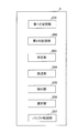
- the CPU #A 2a of the packet processing circuit 1d develops and executes a program stored in the flash memory #A 2d in a memory (not shown), so that the information processing apparatus 1 performs the first storage unit. 201, a second storage unit 202, a determination unit 203, an adjustment unit 204, a storage unit 205, a selection unit 206, and a buffer control unit 207.
- the first storage unit 201 stores in advance a sequence that may cause a failure in hardware such as the SAS card 1f, the LAN card 1g, the USB card 1h, the graphic card 1i, and the power supply control card 1j.
- the second storage unit 202 stores a sequence for avoiding the failure.
- the determination unit 203 determines whether or not the sequence output for the CPU # 1 1a to control the hardware is a sequence stored in the first storage unit 201.
- the adjustment unit 204 stores the sequence output from the CPU # 1 1a in the second storage. Adjustment is performed using the sequence stored in the unit 202.
- the storage unit 205 stores a sequence output by the CPU # 1 1a for controlling the hardware.
- the selection unit 206 selects either the sequence delayed by a predetermined number of sequences via the storage unit 205 or the sequence acquired from the second storage unit 202 corresponding to the sequence stored in the first storage unit 201. To do.
- the buffer control unit 207 controls discarding of the sequence stored in the storage unit 205 and selection by the selection unit 206.
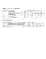
- FIG. 4 shows an outline of an example of information stored in the NVM # A 2c in the present embodiment.
- the area between address 0h and address 1000000h of NVM # A 2c is a program area.
- a program executed by the CPU #A 2a a control program for the packet processing circuit 1d, a copy of a trigger pattern of a process that may cause the above-mentioned failure to a comparison memory, and a pattern generation for the access generation circuit 2f
- a program for executing processing such as copying to a memory and controlling a buffer area is stored.
- the area between the addresses 1000000h and 2000000h is an area in which the trigger condition and the information of the sequence executed when the trigger condition is satisfied are stored.
- the trigger condition is a condition for determining whether or not a sequence that may cause a failure for each of the cards in the information processing apparatus 1 is instructed by the CPU # 1 1a.
- the sequence information is sequence data executed to avoid the failure.
- FIG. 4 shows, as an example, trigger conditions and sequence information related to a sequence commanded from the CPU # 1 1a to the USB card 1h.
- an area between the addresses 2000000000h and 3000000h is an area in which information indicating an area in which the above trigger condition and sequence information is stored is stored. In the area between addresses 3000000h and 4000000h, the history of data written when the above sequence is executed is stored.
- the packet processing circuit 1d triggers condition setting 1 “trigger setup # 1”.
- the sequence for writing data “BB” to the X1 register is added to the USB card 1h according to the sequence described in sequence setting 1 “sequence setup # 1”.
- the packet processing circuit 1d satisfies the trigger condition described in the trigger condition setting 2 “trigger setup # 2”. Then, in the packet processing circuit 1d, according to the sequence described in the sequence setting 2 “sequence setup # 2”, the sequence for writing the data “CC” to the X2 register and the data “XX” to the X3 register for the USB card 1h. The order of the writing sequence is changed. Further, after generating a sequence for writing data “CC” to the X2 register, a sequence for writing data “XX” to the X3 register is generated after a waiting time of 10 ⁇ s.
- FIG. 5 shows an outline of an example of information stored in the flash memory #A 2d in the present embodiment.
- the area between address 0h and address 20000000h of the flash memory #A 2d is an area in which various initialization programs executed by the CPU #A 2a are stored. Examples of data stored in this area include a program that executes initialization of the CPU #A 2a, initialization of the access generation circuit 2f, initialization of the buffer area, and parameters used for each initialization.
- An area between addresses 2000000h and 4000000h is an area in which PCI configuration information of the packet processing circuit 1d is stored.
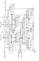
- FIG. 6 shows a schematic configuration of the packet monitoring circuit 2e.
- the packet monitoring circuit 2e includes deserializers 3a and 3b, parallel data latches 3c and 3d, a data synchronization control circuit 3e, trace memories 3f and 3g, N (N is a natural number) comparators #N 3h, 3i, N address counters #N 3j, 3k, N comparison memories #N 3m, 3n, and an internal bus control circuit 3p.
- the comparison memories #N 3m and 3n correspond to an example of the first storage unit.
- the comparators #N 3h and 3i correspond to an example of a determination unit.
- Address counters #N 3j and 3k correspond to an example of an index part.
- comparators #N 3h and 3i, address counters #N 3j and 3k, and comparison memories #N 3m and 3n are paired.
- the deserializers 3a and 3b acquire packets input to the packet processing circuit 1d, and convert the acquired packets from serial data to parallel data. Further, the deserializers 3a and 3b output a signal (Drdy; Data ⁇ Ready) indicating that the conversion of the acquired packet into parallel data is completed. Further, the deserializers 3a and 3b output signals (Packet # A and Packet # B) indicating that packets have been acquired.
- the parallel data latches 3c and 3d latch the parallel data output from the deserializers 3a and 3b based on the Drdy signal. Further, the parallel data latches 3c and 3d cut out and process information included in the packet. Information cut out by the parallel data latches 3c and 3d is used for comparison processing by the comparators #N 3h and 3i.
- FIG. 7 schematically shows a format of a packet processed by the parallel data latches 3c and 3d. As shown in FIG. 7, the packets are classified into a transaction layer, a data link layer, and a physical link layer.
- the packet includes framing information (Frame), sequence number (Sequence #), transaction type (Header), transfer data (Data), transaction layer CRC (Cyclic Redundancy Check) calculation code (RCRC; Read Cyclic Redundancy Check). ), Data link layer RCR calculation code (LCRC; Link Cyclic Redundancy Check), and framing information (Frame).
- the trace memories 3f and 3g store the parallel data latched by the parallel data latches 3c and 3d. Note that data writing to the trace memories 3f and 3g is executed in synchronization with the Drdy signal. Further, reading of data from the trace memories 3f and 3g is executed in synchronization with the Rtm signal output from the data synchronization control circuit 3e.
- the data synchronization control circuit 3e performs synchronization control of data access from the internal bus according to the control of the internal bus control circuit 3p. When the data synchronization control circuit 3e receives a read request signal from the internal bus via the internal bus control circuit 3p, the data synchronization control circuit 3e outputs an Rtm signal.
- the trigger conditions stored in NVM # A 2c are stored in comparison memories #N 3m and 3n. Note that a trigger condition for determining whether one or a plurality of sequences has occurred is stored in one comparison memory of comparison memories #N 3m and 3n.
- the comparison memories #N 3m and 3n receive trigger condition data from the internal bus control circuit 3p.
- the comparators #N 3h and 3i compare the trigger conditions acquired from the comparison memories #N 3m and 3n with the data input from the parallel data latches 3c and 3d. Specifically, the comparators #N 3h and 3i compare the sequence included in the data received from the parallel data latches 3c and 3d with the sequence included in the trigger condition acquired from the comparison memory #N 3m and 3n. , It is determined whether or not the sequences match each other.
- Comparator #N 3h compares the downstream packet input to the packet processing circuit 1d. Further, the comparator #N 3i performs comparison with the upstream packet input to the packet processing circuit 1d. When the comparators #N 3h and 3i determine that the above sequences match as a result of the comparison, the signals Hit-down #N and Hit-up #N (where N is the same as N of the comparator #N) ) Respectively. The comparators #N 3h and 3i output signals Upd # N and Upu # N indicating that the trigger conditions are matched to the address counters #N 3j and 3k, respectively.
- the trigger conditions stored in NVM # A 2c will be described.
- the trigger condition stored in the comparison memory # 1 of the comparison memory #N 3m executes the instruction A.
- the occurrence of a sequence is defined as a first condition
- the occurrence of a sequence for executing an instruction B is included as a second condition.
- the comparator # 1 paired with the comparison memory # 1 performs the comparison process using the first condition and the second condition in order.
- the address counter #N 3j increments the counter value by one.
- the counter value after the increment by the address counter #N 3j is output to the comparison memory #N 3m.
- the counter value of address counter #N 3j is the address of comparison memory #N 3m.
- the a-th condition of the trigger condition is stored at address a (3 is a natural number) of comparison memory #N 3m.
- the comparison memory #N 3m outputs the a-th condition stored at address a to the comparator #N 3h when the counter value input from the address counter #N 3j is a.
- the initial value of the counter value of address counter # 1 of address counter #N 3j is initially set to 1. Further, the first condition and the second condition are stored in the comparison memory # 1 of the comparison memory #N 3m. Then, it is determined that the first condition is matched by the comparator # 1 of the comparator #N 3h. As a result, the address counter # 1 of the address counter #N 3j increments the counter value to 2 by the signal Upd # 1 output from the comparator # 1 of the comparator #N 3h. Address counter # 1 of address counter #N 3j outputs counter value 2 to comparison memory # 1 of comparison memory #N 3m. The comparison memory # 1 of the comparison memory #N 3m reads the second condition based on the counter value 2, and outputs the data of the second condition to the comparator # 1 of the comparator #N 3h.
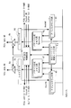
- FIG. 8 shows a schematic configuration of the access generation circuit 2f.
- the access generation circuit 2f includes gates 4a, 4b, serializers 4c, 4d, PCIe output control circuit 4e, N (N is a natural number) pattern generation memory #N 4f, 4g, N addresses It has counters #N 4h, 4i, and N generation sequence control registers #N 4j.
- the pattern generation memories #N 4f and 4g correspond to an example of the second storage unit.
- the generation sequence control register #N 4j corresponds to an example of an adjustment unit.
- Pattern generation memory #N 4f, 4g stores a sequence that is executed when the trigger condition stored in NVM # A 2c is satisfied.
- the pattern generation memories #N 4f and 4g are paired with the comparison memories #N 3m and 3n. Therefore, sequences executed when the trigger conditions stored in the comparison memories #N 3m and 3n are satisfied are stored in the pattern generation memories #N 4f and 4g, respectively.
- the pattern generation memory #N 4f, 4g assembles a transaction layer, a data link layer, and a physical layer and writes back to the pattern generation memory #N 4f, 4g in order to use the sequence data as a PCIe packet. The rewritten data is output to the serializers 4c and 4d.
- the generation sequence control register #N 4j controls the operation of each unit in the access generation circuit 2f in accordance with a command input from the CPU #A 2a of the packet processing circuit 1d via the internal bus.
- the PCIe output control circuit 4e controls the operation timing of the gates 4a and 4b, and outputs signals PCIe control N # A and PCIe control N # B for controlling the purge processing of the buffer A 2h and the buffer B 2i.
- the serializers 4c and 4d convert the parallel data of the sequence input from the pattern generation memory #N 4f and 4g into serial data and output the serial data to the gates 4a and 4b, respectively.
- the sequence stored in the pattern generation memory #N 4f, 4g may have a plurality of processing instructions. For example, when a sequence for executing processing instruction B following processing instruction A is stored in pattern generation memory #N 4f, 4g, pattern generation memory #N 4f, 4g is input from address counter #N 4h, 4i.
- the processing instructions A and B are sequentially output to the serializers 4c and 4d based on the signal designating the address of the pattern generation memory #N 4f and 4g.
- the serializer 4c outputs the timing signal Dset # A to the address counter #N 4h when the sequence processing data input from the pattern generation memory #N of the pattern generation memory #N 4f is output to the gate 4a.
- the address counter #N 4h increments the counter value by 1 when the signal Dset # A is input from the serializer 4c.
- the counter value incremented by the address counter #N 4h is output to the pattern generation memory #N 4f.
- the counter value of address counter #N 4h is the address of pattern generation memory #N 4f.
- the a-th processing instruction is stored at address a of the pattern generation memory #N 4f (a is a natural number).
- the pattern generation memory #N 4f outputs the a-th processing instruction stored at address a to the serializer 4c when the counter value input from the address counter #N 4h is a.
- the initial value of the address counter # 1 of the address counter #N 4h is set to 1. Further, the first processing instruction and the second processing instruction of the sequence are stored in the pattern generation memory # 1 of the pattern generation memory #N 4f. Then, according to the control of the generation sequence control register #N 4j, the pattern generation memory # 1 of the pattern generation memory #N 4f outputs the data of the first processing instruction to the serializer 4c.
- the serializer 4c When the serializer 4c outputs the data of the first processing instruction to the gate 4a, the serializer 4c outputs the signal Dset # A to the address counter # 1 of the address counter #N 4h.
- the address counter # 1 of the address counter #N 4h increments the counter value to 2 when the signal Dset # A is input.
- Address counter # 1 of address counter #N 4h outputs counter value 2 to pattern generation memory # 1 of pattern generation memory #N 4f.
- the pattern generation memory # 1 of the pattern generation memory #N 4f outputs the data of the second processing instruction to the serializer 4c based on the counter value 2.
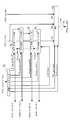
- FIG. 9 shows a schematic configuration of the buffer A 2h.
- the buffer A 2h includes a control code decoder 5a, M (M is a natural number) FIFO (First-In First-Out) multi-stage buffer #M 5b, a driver 5c, and a multiplexer 5d.
- the control code decoder 5a corresponds to an example of a buffer control unit.
- the multiplexer 5d corresponds to an example of a selection unit.
- the control code decoder 5a decodes the buffer control signals PCIe control 0 to N # A from the access generation circuit 2f into control signals for the respective units in the buffer A 2h.
- the FIFO multistage buffer #M 5b stores the signal PCIePCIin ⁇ # 1S input from the CPU # 1 1a to the packet processing circuit 1d via the route complex 1c in units of packets.
- the control code decoder 5a instructs purging of the packet stored in the FIFO multistage buffer #M 5b according to the instruction of the CPU #A 2a.
- the control code decoder 5a controls whether or not to output a packet from PCIe in # 1S / # 2S by using a Truth pass ⁇ gate signal and a Packet select signal, for example, using a truth table shown in FIG.
- FIG. 10 shows an example of a truth table used when the control code decoder 5a purges the packets stored in the FIFO multistage buffer #M 5b, and when the control code decoder 5a performs output control of the multiplexer 5d.
- An example of the truth table used is shown.
- the control code decoder 5a uses FIFO multi-stage buffers # 1 to ## of the FIFO multi-stage buffer #M 5b according to the combination of signals “0” or “1” of PCIe control 0 to 2 # A input from the access generation circuit 2f. 7 purge is performed. If all the signals of PCIe control 0 to 2 # A are “0”, the control code decoder 5a does not purge the FIFO multistage buffer #M 5b.
- the control code decoder 5a controls the output of the multiplexer 5d according to the combination of the signals “0” or “1” of the PCIe control 3-4 # A input from the access generation circuit 2f. As can be seen from the truth table of FIG. 10, the multiplexer 5d outputs one of the input packets A1 to A3 to the driver 5c according to the output control of the control code decoder 5a. When the signals of PCIe control 3 to 4 # A are all “0”, the control code decoder 5a performs control so that the packet is not output from the multiplexer 5d to the driver 5c.
- the multiplexer 5d under the control of the control code decoder 5a, the multiplexer 5d combines the selection of the inputs A1 and A3, so that the delay of the sequence output by the CPU # 1 1a, discarding, replacement between a plurality of sequences, and a plurality Other sequences can be inserted between other sequences.
- a packet including a sequence output by CPU # 1 1a is stored in FIFO multistage buffer #M 5b, a delay due to buffering occurs. Therefore, by causing the multiplexer 5d to select the input A2 under the control of the control code decoder 5a, a delay caused by storing the packet including the sequence output by the CPU # 1 1a in the FIFO multistage buffer #M 5b is generated. Alternatively, it can be output from the packet processing circuit 1d.
- FIFO multi-stage buffer #M 5b is a multi-stage buffer that is FIFO-per-packet, and outputs a Buffer full signal when the buffer status is full.
- the Empty signal indicates a state in which the buffer in the FIFO is empty, and output data from the previous stage can be input.
- Purge packet #N is a signal for clearing the buffer in the target FIFO multistage buffer, and is a signal for performing deletion processing on the target packet to be purged.
- the driver 5c outputs a packet to the PCIe bus according to a command from the PCIe output control circuit 4e of the access generation circuit 2f.
- the multiplexer 5d outputs any of the input packets A1, A2, and A3 to the driver 5c or does not output any of the input packets to the driver 5c according to control by the control code decoder 5a based on the truth table shown in FIG.
- the packet processing circuit 1d when the packet processing circuit 1d deletes a sequence, the sequence is included in the FIFO multistage buffer #M 5b under the control of the CPU #A 2a, the PCIe output control circuit 4e, and the generation sequence control register 4j.
- the purge of the FIFO multistage buffer in which the packet is stored is executed.
- the packet processing circuit 1d changes the sequence, the FIFO multistage buffer storing the packet including the sequence is similarly purged.
- a sequence is generated as PCIe ⁇ data #A and input as the input A3 of the multiplexer 5d, and then output to the PCIe switch 1e via the driver 5c.
- the packet processing circuit 1d adds a sequence
- the packet output from the buffer A 2h is temporarily stopped under the control of the CPU #A 2a, the PCIe output control circuit 4e, and the generation sequence control register 4j.
- an additional sequence is output to the PCIe switch 1e via the PCIe controller 2g.
- the packet processing circuit 1 adjusts the order of the additional sequence and the existing sequence using a so-called proxy response function.
- the control 5 is selected by the multiplexer 5d under the control of the control code decoder 5a. As a result, an additional sequence is output to the PCIe switch 1e.
- buffer B 2i has the same configuration as buffer A 2h, illustration and description thereof are omitted.
- buffer B 2i is configured such that PCIe control #B is input to the control code decoder, PCIe in # 2S is input to FIFO multistage buffer #M 5b, and PCIe data #B is input to the multiplexer. Different from buffer A 2h. Furthermore, the buffer B 2i is different from the buffer A 2h in the configuration shown in FIG. 9 in that Buffer full1 #B is output from the FIFO multistage buffer # 1.
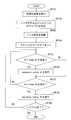
- FIG. 11 shows a flowchart of a processing example executed by the information processing apparatus 1.
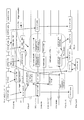
- FIG. 12 shows an example of a time chart when the information processing apparatus 1 executes the processing of the flowchart shown in FIG.
- the CPU #A 2a starts the processing of the flowchart of FIG.
- the intermittent transfer error is, for example, an error between data output and intermittent transfer timing due to a transfer delay in units of packets in the buffer A 2h when data is written to the hardware register. This is a phenomenon in which data cannot be transferred due to matching.
- a sequence of sequence numbers 1 to 6 is output from the CPU # 1 1a to the packet processing circuit 1d.
- the sequence with sequence number 1 is a sequence for writing data “AA” to the X0 register of the USB card 1h.
- the sequence of sequence number 3 is a sequence for writing data “CC” to the X2 register of the USB card 1h.
- the sequence with sequence number 4 is a sequence for writing data “22” to the X3 register of the USB card 1h.
- the information processing apparatus 1 changes to the sequence when the sequence for writing the data “AA” to the X0 register of the USB card 1h occurs in the sequence number 1 as shown in FIG. Subsequently, an additional sequence for writing data “BB” to the X1 register is executed. Further, as shown in FIG. 12, when the sequence for writing the data “CC” to the X2 register occurs in the sequence numbers 3 and 4 as shown in FIG. 12, the information processing apparatus 1 first writes to the X3 register. Execute and write to the X2 register with an interval of 10 ⁇ s or more.
- OP101 when the power of the information processing apparatus 1 is turned on, the boot loader stored in the BIOS ROM (not shown) is executed by the CPU # 1 1a to start the OS and the like. Also, the PCI configuration information stored in the flash memory #A 2d is notified to the CPU # 1 1a by the PCI configuration sequence after startup. Further, the CPU #A 2a reads each processing program stored in the initialization program area stored in the flash memory #A 2d shown in FIG. 5 and executes various initializations. Next, the CPU #A 2a advances the process to OP102. In OP102, the CPU #A 2a reads the program of each process stored in the program area stored in the NVM #A 2c shown in FIG. 5, and executes various processes.
- the CPU #A 2a acquires the trigger condition and sequence data from the USB memory 100 inserted in the USB slot 2b, and creates a trigger / sequence table of the NVM # A 2c using the acquired data. In this processing example, it is assumed that a trigger / sequence table is created as shown in FIG. Next, the CPU #A 2a advances the process to OP103.
- the CPU #A 2a stores the trigger condition stored in the NVM #A 2c in the comparison memory #N 3m and 3n of the packet monitoring circuit 2e. Specifically, the CPU #A 2a uses the trigger condition data “trigger setup # 1” in the trigger / sequence table shown in FIG. 4 in the comparison memory #N of the comparison memory #N of the packet monitoring circuit 2e and the comparison memory # 1. Write to address 0.
- the trigger condition of “trigger setup # 1” is whether or not the sequence output from the CPU # 1 1a to the packet processing circuit 1d is a sequence for writing the data “AA” to the X0 register of the USB card 1h. It is a condition for judging.
- the CPU #A 2a sequentially writes the data of each trigger condition of “trigger setup # 2” from the address 0 of the comparison memory # 2 of the comparison memory #N 3m.
- the trigger condition “trigger setup # 2” the sequence output from the CPU # 1 1a to the packet processing circuit 1d writes the data “XX” (XX is an arbitrary numerical value) to the X2 register of the USB card 1h.
- Conditions for determining whether or not the sequence is included are included.
- whether the trigger condition of “trigger setup # 2” includes a sequence of writing data “CC” to the X3 register of the USB card 1h following the sequence of writing data “XX” to the X2 register of the USB card 1h. Conditions for determining whether or not are included.
- the CPU #A 2a advances the process to OP104.
- the CPU #A 2a resets the address counters #N 3j and 3k of the packet monitoring circuit 3e and the address counters #N 4h and 4i of the access generation circuit 2f.
- the CPU #A 2a causes the multiplexer 5d of the buffer A 2h to select to output the input A1. Further, the CPU #A 2a causes the multiplexer 5d of the buffer B 2i to select to output the input A2.
- the CPU #A 2a advances the process to OP105.
- the CPU #A 2a detects whether or not the Hit-down # 1 signal is input from the packet monitoring circuit 3e.
- the Hit-down # 1 signal is a signal indicating that the trigger condition “trigger setup # 1” stored in the comparison memory # 1 of the comparison memory #N 3 m is satisfied. That is, the Hit-down # 1 signal is a signal indicating that the sequence output from the CPU # 1 1a to the packet processing circuit 1d is determined to be a sequence for writing the data “AA” to the X0 register of the USB card 1h. is there.
- the Hit-down # 1 signal is input (OP105: Yes)
- the CPU #A 2a advances the process to OP106.
- the Hit-down # 1 signal is not input (OP105: No)
- the CPU #A 2a advances the process to OP107.
- the CPU #A 2a executes the processing of the sequence “sequence setup # 1” stored in the NVM # A 2c.
- the sequence “sequence ⁇ setup # 1 ” is a process for adding a process of writing data“ BB ”to the X1 register of the USB card 1h.
- the CPU #A 2a writes a sequence for writing the data “BB” to the X1 register of the USB card 1h in the pattern generation memory # 1 of the pattern generation memory #N 4f.
- the pattern generation memory # 1 of the pattern generation memory #N 4f generates a PCIe packet including the sequence according to the written sequence information.
- the generated packet is output from the packet processing circuit 1d via the PCIe controller 2g.
- the packet output from the packet processing circuit 1d is sent to the USB card 1h via the PCIe switch 1e.
- the USB card 1h executes a process of writing “BB” in the X1 register according to the above-described sequence included in the input packet.
- the CPU #A 2a resets each address counter # 1 of the address counter #N 3j, 4h. Next, the CPU #A 2a advances the process to OP107.
- the CPU #A 2a detects whether or not the Hit-down # 2 signal is input from the packet monitoring circuit 2e.
- the Hit-down # 2 signal is a signal indicating that the trigger condition of “trigger setup # 2” stored in the comparison memory # 2 of the comparison memory #N 3 m is satisfied.
- the Hit-down # 2 signal is the data output to the X3 register of the USB card 1h after the sequence in which the CPU # 1 1a outputs the packet “1” to the X2 register of the USB card 1h. This is a signal indicating that it is determined that the sequence of writing “CC” is continued.
- the Hit-down # 2 signal is input (OP107: Yes)
- the CPU #A 2a advances the process to OP108.
- the Hit-down # 2 signal is not input (OP107: No)
- the CPU #A 2a returns the process to OP105.
- the CPU #A 2a executes the processing of the sequence “sequence setup # 2” stored in the NVM # A 2c.
- the CPU #A 2a first selects the X2 register of the USB card 1h among the packets stored in the FIFO multistage buffer #N in the buffer A 2h. The packet including the sequence of writing and the packet including the sequence of writing to the X3 register are purged.
- the CPU #A 2a reads the sequence number N of the sequence for writing the data “CC” to the X2 register and the data “XX” to be written to the X3 register from the trace memory 3f of the packet monitoring circuit 2e.
- N is 3.
- XX is 22.
- the CPU #A 2a uses the information read out above to store data in the X3 register of the USB card 1h as the sequence number 3.
- the sequence for writing “22” is written to address 0 of pattern generation memory # 2 of pattern generation memory #N 4f.
- the CPU #A 2a sets the sequence number N + 1, that is, the sequence number 4 in the example of FIG. 11 to write the data “CC” to the X2 register of the USB card 1h in the pattern generation memory # 2 of the pattern generation memory # 2 4f. Write to address 1.
- the CPU #A 2a controls the PCIe output control circuit 4e via the generation sequence control register #N 4j, and temporarily stops the packet output of the FIFO multistage buffer #N 5b in the buffer A 2h. The packet output is temporarily stopped because the packets are exchanged as described below. Further, the CPU #A 2a controls the multiplexer 5d to output the packet input from A3.
- the CPU #A 2a controls the generation sequence control register #N 4j to execute the process written in the address 0 of the pattern generation memory # 2 of the pattern generation memory #N 4f.
- a packet including a sequence for writing data “22” to the X3 register of the USB card 1h is output from the pattern generation memory # 2 as the sequence number 3 from the packet processing circuit 1d via the serializer 4c and the multiplexer 5d.
- the CPU #A 2a waits for 10 ⁇ s after the packet including the sequence for writing the data “22” in the X3 register of the USB card 1h is output from the packet processing circuit 1d. Then, the CPU #A 2a controls the generation sequence control register #N 4j to execute the process written in the first address of the pattern generation memory # 2 of the pattern generation memory #N 4f. Accordingly, a packet including a sequence for writing data “CC” to the X2 register of the USB card 1h is output from the pattern generation memory # 2 as the sequence number 4 from the packet processing circuit 1d via the serializer 4c and the multiplexer 5d.
- the CPU #A 2a restarts the packet output of the FIFO multistage buffer #N 5b in the buffer A 2h, and controls the multiplexer 5d to output the packet input from A1.
- the packet including the sequence for writing the data “33” to the X5 register of the USB card 1h inputted as the sequence number 5 from the CPU # 1 1a to the packet processing circuit 1d is converted into the FIFO multistage buffer #.
- the packet is output from the packet processing circuit 1d as the sequence number 5 via the N 5b and the multiplexer 5d.
- the CPU #A 2a resets the address counter #N of the packet monitoring circuit 2e #N 3j and the address counter #N of the access generation circuit 2f #N 4h and resets the address counter # 2.
- a packet including a sequence for writing data “CC” to the X2 register of the USB card 1h input from the CPU # 1 1a to the packet processing circuit 1d as the sequence number 3 is output from the packet processing circuit 1d as the sequence number 4. Is done. Further, a packet including a sequence for writing data “22” in the X3 register of the USB card 1h input from the CPU # 1 1a to the packet processing circuit 1d as the sequence number 4 is output from the packet processing circuit 1d as the sequence number 3. As a result, these two packets are switched by the packet processing circuit 1d and output to the USB card 1h.
- CPU #A 2a executes the process of OP108 described above, the process proceeds to OP109.
- the CPU #A 2a determines whether or not a process for terminating the system of the information processing apparatus 1 has occurred. When processing for terminating the system of the information processing apparatus 1 occurs (OP109: Yes), the CPU #A 2a finishes the processing of this flowchart. If no process for terminating the system of the information processing apparatus 1 has occurred (OP109: No), the CPU #A 2a returns the process to OP105 and repeats the above process.
- the packet processing circuit 1d By executing the above processing, the packet processing circuit 1d detects that the sequence included in the packet output from the CPU # 1 1a satisfies the failure occurrence condition, and performs the sequence according to the detected failure occurrence condition. Adjust the order and timing. Then, the packet processing circuit 1d outputs the adjusted sequence to hardware such as the USB card 1h in the information processing apparatus 1 that is the transmission destination of the packet.
- the processing for the downstream packet has been described. However, the processing for the upstream packet is similarly executed by the component corresponding to each component that processes the downstream packet.
- a sequence for executing a workaround for a failure such as a change in the access order or write data of the memory space, I / O space, deletion or addition of access, or change of access timing for the hardware is packet processing. Registered in the circuit 1d. Thereby, hardware failure avoidance can be centrally managed in the packet processing circuit 1d.
- the configuration and processing of the information processing apparatus 1 and the like are not limited to the above-described embodiment, and are within a range that does not lose the technical idea of the present invention.
- Various changes can be made.
- the trigger conditions and the number of sequences are not limited to the above.
- the third trigger condition and sequence it is possible to perform a determination process similar to OP105 and OP107 and a process similar to OP106 and OP108 to be executed following OP108 in the above flowchart. Good.
- FIG. 13 shows a schematic configuration diagram of the information processing system 10.
- the information processing system 10 includes an information processing apparatus 1000, an I / O controller 2000, and a display 3000.
- the information processing apparatus 1000 includes a CPU # 1 1a, a memory # 1 1b, a route complex 1c, and a packet processing circuit 1d.
- the information processing apparatus 1000 is connected to the I / O controller 2000 by a PCIe cable.
- the I / O controller 2000 corresponds to the peripheral device described above.
- the I / O controller 2000 controls data input / output with respect to the display 3000 in accordance with a sequence input from the information processing apparatus 1000.
- the CPU # 1 1a outputs a sequence for controlling the I / O controller 2000.
- the sequence is a sequence that causes an abnormality in the data input / output timing of the I / O controller 2000 and causes noise on the screen of the display 3000 connected to the I / O controller 2000.
- the packet processing circuit 1c When a packet including the sequence is input to the packet processing circuit 1c, the sequence order and timing are adjusted by the above processing. As a result, the adjusted sequence is transmitted to the I / O controller 2000, so that the above-described obstacles in the I / O controller 2000 can be avoided, and no noise can be generated on the screen of the display 3000.
- the peripheral device connected to the information processing apparatus 1000 is not limited to the I / O controller 2000.
- a management tool for setting the information processing apparatus in a computer or other machine or device (hereinafter referred to as a computer or the like), a program for realizing an OS or the like can be recorded on a computer-readable recording medium.
- the function can be provided by causing a computer or the like to read and execute the program of the recording medium.
- the computer is, for example, an information processing apparatus.
- a computer-readable recording medium is a recording medium that stores information such as data and programs by electrical, magnetic, optical, mechanical, or chemical action and can be read from a computer or the like.
- Examples of such a recording medium that can be removed from a computer or the like include a flexible disk, a magneto-optical disk, a CD-ROM, a CD-R / W, a DVD, a Blu-ray disk, a DAT, an 8 mm tape, a flash memory, and the like.
- cards There are cards.
Landscapes
- Engineering & Computer Science (AREA)
- Theoretical Computer Science (AREA)
- General Engineering & Computer Science (AREA)
- Physics & Mathematics (AREA)
- General Physics & Mathematics (AREA)
- Quality & Reliability (AREA)
- Software Systems (AREA)
- Computer Hardware Design (AREA)
- Debugging And Monitoring (AREA)
- Stored Programmes (AREA)
- Retry When Errors Occur (AREA)
Abstract
Description
コンピュータその他の機械、装置(以下、コンピュータ等)に上記情報処理装置の設定を行うための管理ツール、OSその他を実現させるプログラムをコンピュータ等が読み取り可能な記録媒体に記録することができる。そして、コンピュータ等に、この記録媒体のプログラムを読み込ませて実行させることにより、その機能を提供させることができる。ここで、コンピュータは、例えば、情報処理装置などである。
1a CPU#1
1d パケット処理回路
2a CPU#A
2c NVM#A
2e パケット監視回路
2f アクセス生成回路
2h バッファA
2i バッファB
10 情報処理システム
Claims (7)
- プロセッサにより制御されるデバイスに障害を発生させる場合があるシーケンスをあらかじめ記憶する第1の記憶部と、
前記障害を回避するシーケンスを記憶する第2の記憶部と、
前記プロセッサが前記デバイスを制御するために出力するシーケンスが前記第1の記憶部に記憶されたシーケンスであるか否かを判定する判定部と、
前記プロセッサが前記デバイスを制御するために出力するシーケンスが前記第1の記憶部に記憶されたシーケンスであると判定された場合に、前記プロセッサが前記デバイスを制御するために出力する前記シーケンスを前記第2の記憶部に記憶されたシーケンスを用いて調整する調整部と
を有する情報処理装置。 - 前記第1の記憶部は、前記デバイスに障害を発生させる場合がある複数のシーケンスをあらかじめ記憶し、
前記判定部は、前記プロセッサが前記デバイスを制御するために出力するシーケンスが前記第1の記憶部に記憶されている前記各シーケンスであるか否かの判定を並列に実行する
請求項1に記載の情報処理装置。 - 前記判定部は、前記プロセッサが出力した第1のシーケンスが、前記第1の記憶部の第1のアドレスに記憶されたシーケンスであると判定すると、前記第1のシーケンスに後続する第2のシーケンスが前記第1の記憶部の第2のアドレスに記憶されたシーケンスであるか否かを判定する処理を所定シーケンス数分繰り返す請求項1または2に記載の情報処理装置。
- 前記プロセッサが出力したシーケンスを格納する複数の格納部と、
前記複数の格納部を介して所定シーケンス数遅延したシーケンス、および前記第1の記憶部に記憶されたシーケンスに対応して第2の記憶部から取得されたシーケンスのいずれかを選択する選択部と、
前記複数の格納部に格納されたシーケンスの廃棄と前記選択部による選択とを制御するバッファ制御部をさらに備える
請求項1から請求項3のいずれか1項に記載の情報処理装置。 - 前記バッファ制御部は、前記シーケンスの廃棄と前記選択とによって、前記プロセッサが出力したシーケンスの遅延、廃棄、および複数のシーケンス間の入替、および複数のシーケンス間への他のシーケンスの挿入の少なくとも1つを実行する請求項4に記載の情報処理装置。
- 情報処理装置と前記情報処理装置により使用されるデバイスとを有する情報処理システムにおいて、
前記情報処理装置は、
プロセッサと、
前記プロセッサにより制御される前記デバイスに障害を発生させる場合があるシーケンスをあらかじめ記憶する第1の記憶部と、
前記障害を回避するシーケンスを記憶する第2の記憶部と、
前記プロセッサが前記デバイスを制御するために出力するシーケンスが前記第1の記憶装置に記憶されたシーケンスであるか否かを判定する判定部と、
前記プロセッサが前記デバイスを制御するために出力するシーケンスが前記第1の記憶装置に記憶されたシーケンスであると判定された場合に、前記プロセッサが前記デバイスを制御するために出力する前記シーケンスを前記第2の記憶装置に記憶されたシーケンスを用いて調整する調整部と
を有する情報処理システム。 - 情報処理装置の制御プログラムであって、
前記情報処理装置が有する第1の記憶部に、プロセッサにより制御されるデバイスに障害を発生させる場合があるシーケンスをあらかじめ記憶させ、
前記情報処理装置が有する第2の記憶部に、前記障害を回避するシーケンスを記憶させ、
前記情報処理装置が有する判定部に、前記プロセッサが前記デバイスを制御するために出力するシーケンスが前記第1の記憶部に記憶されたシーケンスであるか否かを判定させ、
前記情報処理装置が有する調整部に、前記プロセッサが前記デバイスを制御するために出力するシーケンスが前記第1の記憶部に記憶されたシーケンスであると判定された場合に、前記プロセッサが前記デバイスを制御するために出力するシーケンスを前記第2の記憶部に記憶されたシーケンスを用いて調整させる
情報処理装置の制御プログラム。
Priority Applications (3)
| Application Number | Priority Date | Filing Date | Title |
|---|---|---|---|
| JP2017507228A JPWO2016151774A1 (ja) | 2015-03-24 | 2015-03-24 | 情報処理装置、情報処理システムおよび情報処理装置の制御プログラム |
| PCT/JP2015/058972 WO2016151774A1 (ja) | 2015-03-24 | 2015-03-24 | 情報処理装置、情報処理システムおよび情報処理装置の制御プログラム |
| US15/712,903 US20180011755A1 (en) | 2015-03-24 | 2017-09-22 | Information processing apparatus for analyzing hardware failure and information processing system therefor |
Applications Claiming Priority (1)
| Application Number | Priority Date | Filing Date | Title |
|---|---|---|---|
| PCT/JP2015/058972 WO2016151774A1 (ja) | 2015-03-24 | 2015-03-24 | 情報処理装置、情報処理システムおよび情報処理装置の制御プログラム |
Related Child Applications (1)
| Application Number | Title | Priority Date | Filing Date |
|---|---|---|---|
| US15/712,903 Continuation US20180011755A1 (en) | 2015-03-24 | 2017-09-22 | Information processing apparatus for analyzing hardware failure and information processing system therefor |
Publications (1)
| Publication Number | Publication Date |
|---|---|
| WO2016151774A1 true WO2016151774A1 (ja) | 2016-09-29 |
Family
ID=56978085
Family Applications (1)
| Application Number | Title | Priority Date | Filing Date |
|---|---|---|---|
| PCT/JP2015/058972 Ceased WO2016151774A1 (ja) | 2015-03-24 | 2015-03-24 | 情報処理装置、情報処理システムおよび情報処理装置の制御プログラム |
Country Status (3)
| Country | Link |
|---|---|
| US (1) | US20180011755A1 (ja) |
| JP (1) | JPWO2016151774A1 (ja) |
| WO (1) | WO2016151774A1 (ja) |
Citations (6)
| Publication number | Priority date | Publication date | Assignee | Title |
|---|---|---|---|---|
| JPH0535470A (ja) * | 1990-08-03 | 1993-02-12 | Matsushita Electric Ind Co Ltd | 命令供給装置 |
| JPH0581014A (ja) * | 1990-08-02 | 1993-04-02 | Internatl Business Mach Corp <Ibm> | マイクロコード訂正のためのオンチツプ制御ストア用プログラム可能アレイ |
| JPH10124328A (ja) * | 1996-10-24 | 1998-05-15 | Nec Corp | 障害回避機構内蔵マイクロプロセッサおよびその障害回 避方法 |
| US20040128590A1 (en) * | 2002-12-30 | 2004-07-01 | Michael Derr | Patch mechanism |
| JP2004326594A (ja) * | 2003-04-25 | 2004-11-18 | Toshiba Microelectronics Corp | 命令拡張回路、マイクロプロセッサ及び命令拡張方法 |
| JP2012208623A (ja) * | 2011-03-29 | 2012-10-25 | Konica Minolta Business Technologies Inc | 管理システム、処理装置、および管理方法 |
Family Cites Families (6)
| Publication number | Priority date | Publication date | Assignee | Title |
|---|---|---|---|---|
| US5446851A (en) * | 1990-08-03 | 1995-08-29 | Matsushita Electric Industrial Co., Ltd. | Instruction supplier for a microprocessor capable of preventing a functional error operation |
| JP4190114B2 (ja) * | 1999-11-10 | 2008-12-03 | 株式会社ルネサステクノロジ | マイクロコンピュータ |
| JP3729087B2 (ja) * | 2001-05-23 | 2005-12-21 | 日本電気株式会社 | マルチプロセッサシステム、データ依存投機実行制御装置およびその方法 |
| US8499304B2 (en) * | 2009-12-15 | 2013-07-30 | At&T Mobility Ii Llc | Multiple mode mobile device |
| US8645746B2 (en) * | 2010-12-03 | 2014-02-04 | International Business Machines Corporation | Cable redundancy and failover for multi-lane PCI express IO interconnections |
| WO2015045062A1 (ja) * | 2013-09-26 | 2015-04-02 | 三菱電機株式会社 | 通信システム、待機装置、通信方法及び待機プログラム |
-
2015
- 2015-03-24 JP JP2017507228A patent/JPWO2016151774A1/ja active Pending
- 2015-03-24 WO PCT/JP2015/058972 patent/WO2016151774A1/ja not_active Ceased
-
2017
- 2017-09-22 US US15/712,903 patent/US20180011755A1/en not_active Abandoned
Patent Citations (6)
| Publication number | Priority date | Publication date | Assignee | Title |
|---|---|---|---|---|
| JPH0581014A (ja) * | 1990-08-02 | 1993-04-02 | Internatl Business Mach Corp <Ibm> | マイクロコード訂正のためのオンチツプ制御ストア用プログラム可能アレイ |
| JPH0535470A (ja) * | 1990-08-03 | 1993-02-12 | Matsushita Electric Ind Co Ltd | 命令供給装置 |
| JPH10124328A (ja) * | 1996-10-24 | 1998-05-15 | Nec Corp | 障害回避機構内蔵マイクロプロセッサおよびその障害回 避方法 |
| US20040128590A1 (en) * | 2002-12-30 | 2004-07-01 | Michael Derr | Patch mechanism |
| JP2004326594A (ja) * | 2003-04-25 | 2004-11-18 | Toshiba Microelectronics Corp | 命令拡張回路、マイクロプロセッサ及び命令拡張方法 |
| JP2012208623A (ja) * | 2011-03-29 | 2012-10-25 | Konica Minolta Business Technologies Inc | 管理システム、処理装置、および管理方法 |
Also Published As
| Publication number | Publication date |
|---|---|
| JPWO2016151774A1 (ja) | 2018-01-11 |
| US20180011755A1 (en) | 2018-01-11 |
Similar Documents
| Publication | Publication Date | Title |
|---|---|---|
| JP5107880B2 (ja) | データ転送処理装置及び方法 | |
| US11175977B2 (en) | Method and system to detect failure in PCIe endpoint devices | |
| US8234463B2 (en) | Data processing apparatus, memory controller, and access control method of memory controller | |
| CN111258493B (zh) | 控制器、存储器控制器、存储设备以及操作控制器的方法 | |
| JP4966404B2 (ja) | メモリ制御装置、記憶装置、及びメモリ制御方法 | |
| US20150301886A1 (en) | Information processing apparatus, system, and information processing method | |
| US9191030B2 (en) | Memory controller, data storage device, and memory controlling method | |
| EP3198459A1 (en) | Memory write management in a computer system | |
| JP2011133473A (ja) | 試験装置、試験方法およびプログラム | |
| US11199992B2 (en) | Automatic host buffer pointer pattern detection | |
| TW201945930A (zh) | 使用標準化資料儲存及擷取協定的用於資料編碼及解碼之方法及設備 | |
| JPWO2008053709A1 (ja) | 半導体集積回路選別試験装置および方法 | |
| US20100293418A1 (en) | Memory device, data transfer control device, data transfer method, and computer program product | |
| JP6568012B2 (ja) | メモリ管理システム、方法、およびコンピュータ・プログラム | |
| JP2013257640A (ja) | コンフィグレーション制御装置、コンフィグレーション制御方法及びコンフィグレーション制御プログラム | |
| US20130238881A1 (en) | Data transmission device, data transmission method, and computer program product | |
| US11450398B2 (en) | Method of testing slave device of inter-integrated circuit bus | |
| US8943255B2 (en) | Methods and structure for accounting for connection resets between peripheral component interconnect express bridges and host devices | |
| US8291270B2 (en) | Request processing device, request processing system, and access testing method | |
| US9753876B1 (en) | Processing of inbound back-to-back completions in a communication system | |
| WO2016151774A1 (ja) | 情報処理装置、情報処理システムおよび情報処理装置の制御プログラム | |
| US10795797B2 (en) | Controller, SATA system and method of operation therefor | |
| TWI648620B (zh) | 記憶體裝置以及操作指令錯誤處理方法 | |
| CN116302203A (zh) | 一种ras功能的配置方法、装置、电子设备和介质 | |
| US20170206178A1 (en) | Information processing apparatus, method of transferring data, and non-transitory computer-readable recording medium |
Legal Events
| Date | Code | Title | Description |
|---|---|---|---|
| 121 | Ep: the epo has been informed by wipo that ep was designated in this application |
Ref document number: 15886327 Country of ref document: EP Kind code of ref document: A1 |
|
| ENP | Entry into the national phase |
Ref document number: 2017507228 Country of ref document: JP Kind code of ref document: A |
|
| NENP | Non-entry into the national phase |
Ref country code: DE |
|
| ENP | Entry into the national phase |
Ref document number: 2015388270 Country of ref document: AU Date of ref document: 20150324 Kind code of ref document: A |
|
| 122 | Ep: pct application non-entry in european phase |
Ref document number: 15886327 Country of ref document: EP Kind code of ref document: A1 |