WO2016145493A1 - Method and system for polarisation division multiplexed optical transmission - Google Patents
Method and system for polarisation division multiplexed optical transmission Download PDFInfo
- Publication number
- WO2016145493A1 WO2016145493A1 PCT/AU2016/050192 AU2016050192W WO2016145493A1 WO 2016145493 A1 WO2016145493 A1 WO 2016145493A1 AU 2016050192 W AU2016050192 W AU 2016050192W WO 2016145493 A1 WO2016145493 A1 WO 2016145493A1
- Authority
- WO
- WIPO (PCT)
- Prior art keywords
- complex
- optical
- polarisation
- symbol sets
- symbol
- Prior art date
- Legal status (The legal status is an assumption and is not a legal conclusion. Google has not performed a legal analysis and makes no representation as to the accuracy of the status listed.)
- Ceased
Links
Classifications
-
- H—ELECTRICITY
- H04—ELECTRIC COMMUNICATION TECHNIQUE
- H04J—MULTIPLEX COMMUNICATION
- H04J14/00—Optical multiplex systems
- H04J14/06—Polarisation multiplex systems
-
- H—ELECTRICITY
- H04—ELECTRIC COMMUNICATION TECHNIQUE
- H04B—TRANSMISSION
- H04B10/00—Transmission systems employing electromagnetic waves other than radio-waves, e.g. infrared, visible or ultraviolet light, or employing corpuscular radiation, e.g. quantum communication
- H04B10/25—Arrangements specific to fibre transmission
- H04B10/2507—Arrangements specific to fibre transmission for the reduction or elimination of distortion or dispersion
- H04B10/2572—Arrangements specific to fibre transmission for the reduction or elimination of distortion or dispersion due to forms of polarisation-dependent distortion other than PMD
-
- H—ELECTRICITY
- H04—ELECTRIC COMMUNICATION TECHNIQUE
- H04B—TRANSMISSION
- H04B10/00—Transmission systems employing electromagnetic waves other than radio-waves, e.g. infrared, visible or ultraviolet light, or employing corpuscular radiation, e.g. quantum communication
- H04B10/50—Transmitters
- H04B10/501—Structural aspects
- H04B10/503—Laser transmitters
- H04B10/505—Laser transmitters using external modulation
- H04B10/5053—Laser transmitters using external modulation using a parallel, i.e. shunt, combination of modulators
-
- H—ELECTRICITY
- H04—ELECTRIC COMMUNICATION TECHNIQUE
- H04B—TRANSMISSION
- H04B10/00—Transmission systems employing electromagnetic waves other than radio-waves, e.g. infrared, visible or ultraviolet light, or employing corpuscular radiation, e.g. quantum communication
- H04B10/50—Transmitters
- H04B10/516—Details of coding or modulation
-
- H—ELECTRICITY
- H04—ELECTRIC COMMUNICATION TECHNIQUE
- H04B—TRANSMISSION
- H04B10/00—Transmission systems employing electromagnetic waves other than radio-waves, e.g. infrared, visible or ultraviolet light, or employing corpuscular radiation, e.g. quantum communication
- H04B10/50—Transmitters
- H04B10/516—Details of coding or modulation
- H04B10/548—Phase or frequency modulation
- H04B10/556—Digital modulation, e.g. differential phase shift keying [DPSK] or frequency shift keying [FSK]
- H04B10/5561—Digital phase modulation
-
- H—ELECTRICITY
- H04—ELECTRIC COMMUNICATION TECHNIQUE
- H04B—TRANSMISSION
- H04B10/00—Transmission systems employing electromagnetic waves other than radio-waves, e.g. infrared, visible or ultraviolet light, or employing corpuscular radiation, e.g. quantum communication
- H04B10/60—Receivers
- H04B10/61—Coherent receivers
- H04B10/616—Details of the electronic signal processing in coherent optical receivers
Definitions
- the present invention relates generally to optical communications, and more particularly to a method and apparatus for improving the quality of reception of polarisation division multiplexed (PDM) optical signals in the presence of polarisation-dependent loss (PDL).
- PDM polarisation division multiplexed
- Optical transmission in which an information signal is modulated onto an optical carrier, is widely employed in modern communications systems.
- wide area communications networks employ long-haul transmission links using single-mode optical fibres for the transmission of digital information at very high bit-rates (e.g. up to and beyond 100 Gb/s per wavelength), using one or more optical carriers, or wavelengths, over each fibre.
- bit-rates e.g. up to and beyond 100 Gb/s per wavelength
- Polarisation division multiplexing in which different information is transmitted on each of two orthogonal polarisation states, is employed in high bit-rate systems to double the transmission capacity of each channel.
- PDL causes non-orthogonality and amplified spontaneous emission (ASE) depolarisation of PDM signals.
- the non-orthogonality can be equalised by an adaptive PMD equaliser.
- depolarised ASE noise degrades the optical signal-to-noise ratio (OSNR) of the lossy polarisation state, and errors in the received signal in the lossy state dominate the overall system performance.
- OSNR optical signal-to-noise ratio
- the invention provides a method of transmitting digital information over an optical channel comprising:
- the method implements a pairwise coding of transmitted symbols across the two polarisation states.
- the invention is based on the novel insight that PDL may be viewed as a form of 'polarisation-selective fading', analogous to frequency-dependent fading in wireless RF systems.
- pairwise coding does not involve any additional overhead and therefore does not impact on payload data rate, and requires only a few extra computations per symbol, because only pairs of symbols are processed together.
- a complementary aspect of the invention provides a method of recovering digital information modulated onto first and second polarisation states of an optical carrier and transmitted over an optical channel, the method comprising:
- the invention provides an optical transmitter comprising:
- a digital processor configured to:
- DAC digital-to-analog conversion
- an optical carrier source having first and second polarisation states, coupled to first and second modulation units, the first modulation unit being configured to modulate in-phase (I) and quadrature (Q) components of the first polarisation state of the optical source with the first and third electrical signals, respectively, and the second modulation unit being configured to modulate in- phase (I) and quadrature (Q) components of the second polarisation state with the second and fourth electrical signals, respectively.
- the invention provides an optical receiver, configured to recover digital information modulated onto first and second polarisation states of an optical carrier and transmitted over an optical channel, the receiver comprising a digital processor configured to:
- OSNR optical signal-to-noise ratio
- FIG. 1 is a schematic diagram of an optical transmission system embodying the invention
- Figure 2 is a schematic diagram of a proof-of-concept experimental demonstration corresponding with the system of Figure 1 ;
- Figure 3 shows a spectrum of first and second polarisation states of the optical signal generated in the demonstration system of Figure 2;
- Figure 4 is a graph of OSNR penalty as a function of PDL
- Figure 5 is a graph of received signal quality factor for each channel of a wavelength division multiplexed (WDM) signal generated in the demonstration system of Figure 2;
- Figure 6 shows exemplary constellation diagrams of a received signal, generated within the demonstration system of Figure 2.
- FIG. 1 there is shown schematically a system 100 for
- a transmitter 101 receives input digital information bits 102 which are selectively divided via a 1-2 demultiplexer 104.
- the resulting bit sequences are input to corresponding mapping units 106, 108.
- Each mapping unit 106, 108 maps groups of input bits to corresponding complex-valued symbols.
- a number of different symbol mappings may be employed by embodiments of the invention, including, without limitation, quadrature phase shift keying (QPSK) or quadrature amplitude modulation (QAM) mappings. Different mappings, and/or different numbers of levels, may be selected depending upon the available signal-to-noise ratio, and the number of bits to be encoded within each mapped symbol.
- QPSK quadrature phase shift keying
- QAM quadrature amplitude modulation
- ⁇ represents the ratio between the OSNR in the 'good' polarisation state to the OSNR in the 'bad' polarisation state. This rotation angle is designed to minimise the bit error rate (BER) for a given OSNR difference between the two polarisation states.
- BER bit error rate
- Interleaving is performed following angle rotation.
- the real parts of the rotated symbol values are input to digital-to-analog converters (DACs) 1 14, 1 16, while the imaginary parts are input to DACs 1 16, 120.
- the outputs of DACs 1 14, 1 16 comprise the in-phase (I) and quadrature (Q) components to be modulated onto a first polarisation state of the transmitted signal, while the outputs of DACs 1 18, 120 comprise I and Q components of a signal to be modulated onto a second polarisation state of the transmitted signal.
- a PDM optical signal source comprises an optical carrier source 122, a polarisation beam splitter 124, and a pair of l/Q (complex) modulators 126, 128.
- the I and Q components output from DACs 1 14, 1 16 are input to modulator 126, thereby modulating the first polarisation state of the optical carrier source 122.
- the outputs of DACs 1 18, 120 are input to modulator 128, thereby modulating the second polarisation state of the optical carrier 122.
- the modulated polarisation states are recombined in polarisation beam splitter 130, to produce the PDM optical signal which is transmitted through an optically-amplified transmission link 132.
- the system 100 further comprises a receiver 133 which is configured to recover the transmitted information bits 102.
- the transmitted PDM signal is detected, for example using a dual-polarisation coherent detector 134.
- the detector 134 may comprise, for example, a local oscillator laser source, a pair of optical hybrid circuits, and four pairs of balanced detectors, resulting in the detection of in-phase and quadrature components of the signals transmitted on the two polarisation states.
- the detected in-phase and quadrature components of the first polarisation state are input to analog-to-digital converters (ADCs) 136, 138, while the corresponding I and Q components of the second polarisation state are input to ADCs 140, 142. This results in four corresponding sequences of digitised samples, which are subject to front-end processing 144 within a digital signal processing (DSP) unit.
- DSP digital signal processing
- the front-end DSP processes include front-end correction, clock recovery, channel impairment compensation and carrier recovery.
- the outputs from the front-end processing comprise a pair of equalised complex-valued sample sequences, i.e. real and imaginary parts corresponding with the I and Q components of the two received polarisation states respectively.
- the equalised symbol values corresponding with the first polarisation state are input to OSNR estimation and scaling block 146, while the equalised symbol values corresponding with the second polarisation state are input to OSNR estimation and scaling block 148.
- OSNR estimation and scaling block 146 the equalised symbol values corresponding with the second polarisation state are input to OSNR estimation and scaling block 148.
- the corresponding OSNR is estimated, for example using the statistical moments method as described by C Zhu et al, 'Statistical Moments Based OSNR
- the equalised symbols are then rescaled differently, according to the estimated OSNR of each polarisation.
- the equalised symbols are multiplied by the square root of the estimated OSNR.
- the OSNR varies as a result of the stochastic nature of PDL, and therefore the OSNR estimation and rescaling should be updated periodically, in accordance with the associated state-of-polarisation rotation rate. Typically, a few thousand updates per second (i.e. kHz update rate) should be sufficient for transmission fibre having fast state-of-polarisation rotation.
- the outputs of OSNR estimation and scaling blocks 146, 148 comprise real and imaginary parts of the corresponding rescaled and equalised symbols.
- the interleaving and data recovery are performed by inputting the real parts of the rescaled symbols to maximum likelihood detector (MLD) block 150, while the imaginary parts are input to MLD block 152.
- MLD maximum likelihood detector
- C k is the constellation alphabet (i.e. [1 +j, 1 -j, -1 +j, -1-j] for QPSK modulation) and D k are the rotated and rescaled symbol values.
- the resulting decisions represent information bits that are recombined in multiplexer 154 in order to recover the output bit sequence 156.
- a bit error rate (BER) may be determined by comparing the recovered output bits 156 with the original transmitted input bits 102.
- the presently disclosed embodiments of the invention are implemented substantially via digital signal processing. Such processing is performed both in the transmitter 101 and in the receiver 133.
- the various signal processing blocks shown in the exemplary embodiment 100 represent conceptual processing functions, which may be implemented, in practice, in a variety of different ways, as will be apparent to persons skilled in the art of signal processing.
- the digital processing may be implemented in software executing on a suitable central processing unit (e.g. a DSP device), or as a custom, or semi- custom, hardware unit, such as an application-specific integrated circuit (ASIC), or programmable hardware, such as a field programmable gate array (FPGA).
- a suitable central processing unit e.g. a DSP device
- ASIC application-specific integrated circuit
- FPGA field programmable gate array
- FIG. 2 is a schematic diagram showing the configuration 200 of a proof-of-concept experimental demonstration corresponding with the exemplary system of Figure 1 .
- Eight external cavity lasers (ECLs) 202 having a 50 GHz carrier spacing, are multiplexed with an 8x1 polarisation-maintaining (PM) coupler 204.
- the carrier waves are amplified using a polarisation-maintaining erbium- doped fibre amplifier (PM-EDFA) 206.
- An arbitrary waveform generator (AWG) 208 is used to generate baseband signals at 10 GSa/s, with either conventional PDM-QPSK, or polarisation pairwise coding QPSK (PPC-QPSK) embodying the invention.
- a pair of electrical amplifiers 210 is used to amplify the I and Q components of the signal generated by the AWG 208, which are then used to drive an optical l/Q modulator 212.
- the resulting modulated signals are amplified using a further PM-EDFA 214.
- a PDM emulator 216 is used to delay the ⁇ polarisation state of the optical signal with respect to the 'X' polarisation state.
- the delay was equivalent to 195 symbols, enabling the single AWG 208 to be used to generate dual-polarisation signals. This is illustrated schematically by the blocks 228, which show that the desired PDM signals, suitable for decoding at the receiver, occupy alternate 195 symbol blocks.
- the resulting optical signal is divided into its two polarisation states by polarisation beam splitter (PBS) 218.
- a frequency/channel-dependent PDL is generated using a Finisar WaveShaper (WS) 220, while a variable attenuator 222 is used to match the insertion loss of WS 220.
- the two polarisation states are recombined in PBC 224.
- the resulting PDL-emulated signal is passed through a 50 GHz interleaver 226, and a further optical amplifier 230, before entering a recirculating loop 232.
- the recirculating loop 232 comprises two acousto-optic modulator (AOM) switches, 640 km of standard single-mode fibre, consisting of six 80 km spans and associated optical amplifiers, a gain-flattening WS, and a polarisation scrambler.
- AOM acousto-optic modulator
- an ASE source 234 is used to add optical noise, e.g. to control the OSNR for single-channel back-to-back measurements.
- a further WS 236 is used to select the desired channel for coherent detection.
- the detection is performed by receiver 238, which generates four outputs (i.e. I and Q components of each of the X and Y polarisation states) which are sampled and digitised by a real-time oscilloscope 240.
- the resulting signals can be processed offline, in accordance with conventional PDM-QPSK processing techniques, or according to PPC-QPSK techniques embodying the invention.
- Figure 3 shows a graph 300, comprising the spectrum of X and Y polarisation states of the WDM optical signal generated and transmitted into the recirculating loop 232 of the system 200 shown in Figure 2.
- the spectrum 300 shows wavelength on the horizontal axis 302, and corresponding power on the vertical axis 304.
- the higher-quality (Y) polarisation state is shown by the trace 306, while the lower-quality (X) polarisation state is shown by the trace 308.
- Figure 4 shows a graph 400 of OSNR penalty as a function of PDL.
- PDL in dB
- OSNR penalty for a BER of 10 ⁇ 3 is shown on the vertical axis 404.
- the BER is based on averaging across the two polarisation states. The measurements were performed for a single channel operating in back-to-back mode, i.e. without recirculation in the loop 232, and with added ASE generated by the source 234.
- the PDM-QPSK experimental results closely match the simulation results for worst case PDL, with a 3.5 dB OSNR penalty occurring for a PDL value of 7 dB.
- a PPC-QPSK signal, embodying the invention and using a ⁇ /4 rotation angle outperforms the PDM-QPSK signal significantly, show it just over 1 dB OSNR penalty with 7 dB PDL.
- differences between the ⁇ /4 rotation angle and optimum angle, for PDL less than 7 dB are not significant. This demonstrates that a fixed rotation angle can be used for all cases, thereby avoiding the need to feed back OSNR estimates from the receiver to the transmitter.
- FIG. 5 shows a graph 500 of received signal quality factor for each of the eight WDM channels transmitted using the experimental configuration 200.
- the horizontal axis 502 shows channel index, while the vertical axis 504 shows quality factor, defined as:
- Figure 6 shows exemplary constellation diagrams 600 of a received signal embodying the invention. These constellation diagrams are, respectively: received signal in the X polarisation after equalisation (602); received signal in the Y polarisation after equalisation (604); the received signal in the X polarisation after rescaling (606); the received signal in the Y polarisation after rescaling (608); and the received signals following de-interleaving (610, 612).
- embodiments of the invention employ polarisation pairwise coding for PDM coherent optical signals, improving transmission performance in the presence of PDL.
- the principles of rotating the original information symbols and interleaving the real and imaginary components between two polarisation states are employed.
- the detected X and Y polarisation signals are rescaled according to respective OSNRs, and de-interleaved.
- the overall decoded signals extracted from the two polarisation states have similarly low error rates, and the overall performance is always superior to that of conventionally (non-pairwise-coded) PDM signals, which are dominated by high error rates in the poor quality polarisation state.
- An experimental proof-of-concept demonstration establishes that greatly enhanced overall system performance can be achieved, over a wide range of PDL, without any coding overhead, for single channel and WDM transmission systems.
- mapping methods other than QPSK may be employed, such as QAM, or other multi-level mapping techniques.
- QAM quadrature mapping technique
Landscapes
- Physics & Mathematics (AREA)
- Engineering & Computer Science (AREA)
- Computer Networks & Wireless Communication (AREA)
- Signal Processing (AREA)
- Electromagnetism (AREA)
- Optics & Photonics (AREA)
- Optical Communication System (AREA)
Abstract
A method of transmitting digital information over an optical channel (132) includes mapping (106, 108) input digital information bits to first and second complex-valued symbol sets. A complex rotation (110, 112) is applied to each symbol of the first and second complex-valued symbol sets. In-phase (I) and quadrature (Q) components of a first polarisation state of an optical carrier (122) are modulated with the real parts of the first and second complex-valued symbol sets respectively, while in-phase (I) and quadrature(Q) components of a second polarisation state of the optical carrier are modulated with the imaginary parts of the first and second complex-valued symbol sets respectively.
Description
METHOD AND SYSTEM FOR POLARISATION DIVISION MULTIPLEXED OPTICAL TRANSMISSION
FIELD OF THE INVENTION
[0001 ] The present invention relates generally to optical communications, and more particularly to a method and apparatus for improving the quality of reception of polarisation division multiplexed (PDM) optical signals in the presence of polarisation-dependent loss (PDL).
BACKGROUND TO THE INVENTION
[0002] Optical transmission, in which an information signal is modulated onto an optical carrier, is widely employed in modern communications systems. In particular, wide area communications networks employ long-haul transmission links using single-mode optical fibres for the transmission of digital information at very high bit-rates (e.g. up to and beyond 100 Gb/s per wavelength), using one or more optical carriers, or wavelengths, over each fibre. Furthermore, it is anticipated that higher bit-rates-per-channel will be deployed in future
transmission systems. Polarisation division multiplexing (PDM), in which different information is transmitted on each of two orthogonal polarisation states, is employed in high bit-rate systems to double the transmission capacity of each channel.
[0003] The maximum distance over which data may be transmitted in single- mode optical fibres employing optical amplification, before some form of regeneration is required, is substantially limited by transmission impairments including chromatic dispersion, polarisation mode dispersion (PMD) and nonlinear processes. In PDM systems, polarisation-dependent loss (PDL) is also a significant impairment.
[0004] In recent years, powerful digital signal processing (DSP) techniques have been developed for use in coherent optical transmission systems, which enable effective compensation or mitigation of most system impairments to be performed within the electronic domain. To date, however, signal degradation due to PDL has not been effectively compensated using DSP. Following long- haul transmission, an accumulated PDL of several dB can occur, and this may become the primary system performance-limiting factor.
[0005] In particular, PDL causes non-orthogonality and amplified spontaneous emission (ASE) depolarisation of PDM signals. The non-orthogonality can be equalised by an adaptive PMD equaliser. However, depolarised ASE noise degrades the optical signal-to-noise ratio (OSNR) of the lossy polarisation state, and errors in the received signal in the lossy state dominate the overall system performance.
[0006] Accordingly, there remains a need in long-haul PDM coherent optical systems for methods and apparatus capable of improving overall system performance in the presence of PDL. The present invention addresses this need.
SUMMARY OF THE INVENTION
[0007] In one aspect, the invention provides a method of transmitting digital information over an optical channel comprising:
mapping input digital information bits to first and second complex- valued symbol sets;
applying a complex rotation to each symbol of the first and second complex-valued symbol sets;
modulating in-phase (I) and quadrature (Q) components of a first polarisation state of an optical carrier with the real parts of the first and second complex-valued symbol sets respectively; and
modulating in-phase (I) and quadrature (Q) components of a second
polarisation state of the optical carrier with the imaginary parts of the first and second complex-valued symbol sets respectively.
[0008] As will be disclosed in greater detail in the following description of embodiments of the invention, the method implements a pairwise coding of transmitted symbols across the two polarisation states. The invention is based on the novel insight that PDL may be viewed as a form of 'polarisation-selective fading', analogous to frequency-dependent fading in wireless RF systems.
Embodiments of the invention thus employ constellation rotation and
real/imaginary interleaved pre-coding in order to improve overall bit-error-rate (BER) performance.
[0009] Advantageously, the use of pairwise coding does not involve any additional overhead and therefore does not impact on payload data rate, and requires only a few extra computations per symbol, because only pairs of symbols are processed together. By interleaving the real (I) and imaginary (Q)
components of both polarisations, only the I or the Q component of each polarisation suffers from 'polarisation-selective fading' at any one time, while the other component maintains a superior OSNR. The effect of ASE depolarisation is mitigated by an effective 'reassignment' of ASE noise from the lossy polarisation to the other polarisation, via the de-interleaving process in the receiver.
[0010] In order to achieve these benefits, a complementary aspect of the invention provides a method of recovering digital information modulated onto first and second polarisation states of an optical carrier and transmitted over an optical channel, the method comprising:
receiving a first complex-valued symbol set wherein the real and imaginary parts of each symbol comprise equalised samples of respective in- phase (I) and quadrature (Q) components of a signal modulated onto the first polarisation state of the optical carrier;
receiving a second complex-valued symbol set wherein the real and imaginary parts of each symbol comprise equalised samples of respective in- phase (I) and quadrature (Q) components of a signal modulated onto the second
polarisation state of the optical carrier;
computing, from the first complex-valued symbol set, a first estimated optical signal-to-noise ratio (OSNR) value of the signal modulated onto the first polarisation state of the optical carrier and, from the second complex-valued symbol set, a second estimated OSNR value of the signal modulated onto the second polarisation state of the optical carrier;
scaling symbols of the first and second complex-valued symbol sets according to the first and second estimated OSNR values to generate respective first and second scaled symbol sets; and
recovering a first sequence of digital information bits from the real parts of the first and second scaled symbol sets, and a second sequence of digital information bits from the imaginary parts of the first and second scaled symbol sets.
[001 1 ] In another aspect, the invention provides an optical transmitter comprising:
a digital processor configured to:
map input digital information bits to first and second complex-valued symbol sets;
apply a complex rotation to each symbol of the first and second complex-valued symbol sets to generate corresponding first and second rotated symbol sets; and
output real and imaginary parts of the first and second rotated symbol sets,
a digital-to-analog conversion (DAC) unit, operatively coupled to the digital processor, configured to receive the real part of the first rotated symbol set, the imaginary part of the first rotated symbol set, the real part of the second rotated symbol set, and the imaginary part of the second rotated symbol set, respectively, and to generate corresponding first, second, third and fourth electrical signals; and
an optical carrier source having first and second polarisation states, coupled to first and second modulation units, the first modulation unit being configured to modulate in-phase (I) and quadrature (Q) components of the first
polarisation state of the optical source with the first and third electrical signals, respectively, and the second modulation unit being configured to modulate in- phase (I) and quadrature (Q) components of the second polarisation state with the second and fourth electrical signals, respectively.
[0012] In yet another aspect, the invention provides an optical receiver, configured to recover digital information modulated onto first and second polarisation states of an optical carrier and transmitted over an optical channel, the receiver comprising a digital processor configured to:
receive a first complex-valued symbol set wherein the real and imaginary parts of each symbol comprise equalised samples of respective in- phase (I) and quadrature (Q) components of a signal modulated onto the first polarisation state of the optical carrier;
receive a second complex-valued symbol set wherein the real and imaginary parts of each symbol comprise equalised samples of respective in- phase (I) and quadrature (Q) components of a signal modulated onto the second polarisation state of the optical carrier;
compute, from the first complex-valued symbol set, a first estimated optical signal-to-noise ratio (OSNR) value of the signal modulated onto the first polarisation state of the optical carrier and, from the second complex-valued symbol set, a second estimated OSNR value of the signal modulated onto the second polarisation state of the optical carrier;
scale symbols of the first and second complex-valued symbol sets according to the first and second estimated OSNR values to generate respective first and second scaled symbol sets; and
recover a first sequence of digital information bits from the real parts of the first and second scaled symbol sets, and a second sequence of digital information bits from the imaginary parts of the first and second scaled symbol sets.
[0013] Further features, properties and benefits of the invention will be apparent from the following description of embodiments, which is provided by way of example in order to illustrate the principles of the invention. The described
embodiments are not intended to limit the scope of the invention, as defined in any of the preceding statements, or in the claims appended hereto.
BRIEF DESCRIPTION OF THE DRAWINGS
[0014] Embodiments of the invention will be described with reference to the accompanying drawings, in which:
Figure 1 is a schematic diagram of an optical transmission system embodying the invention;
Figure 2 is a schematic diagram of a proof-of-concept experimental demonstration corresponding with the system of Figure 1 ;
Figure 3 shows a spectrum of first and second polarisation states of the optical signal generated in the demonstration system of Figure 2;
Figure 4 is a graph of OSNR penalty as a function of PDL;
Figure 5 is a graph of received signal quality factor for each channel of a wavelength division multiplexed (WDM) signal generated in the demonstration system of Figure 2; and
Figure 6 shows exemplary constellation diagrams of a received signal, generated within the demonstration system of Figure 2.
DETAILED DESCRIPTION OF EMBODIMENTS
[0015] In Figure 1 , there is shown schematically a system 100 for
communicating digital information over a PDM optical channel.
[0016] A transmitter 101 receives input digital information bits 102 which are selectively divided via a 1-2 demultiplexer 104. The resulting bit sequences are input to corresponding mapping units 106, 108. Each mapping unit 106, 108 maps groups of input bits to corresponding complex-valued symbols. A number of different symbol mappings may be employed by embodiments of the invention, including, without limitation, quadrature phase shift keying (QPSK) or quadrature amplitude modulation (QAM) mappings. Different mappings, and/or different
numbers of levels, may be selected depending upon the available signal-to-noise ratio, and the number of bits to be encoded within each mapped symbol.
[0017] A complex rotation is then applied to each symbol, as represented by the rotation blocks 1 10, 1 12 in the transmitter 101 . This results in corresponding rotated symbols, given by:
Xe
(1 ) Ye
[0018] In equation (1 ) the input symbols are represented by X and Y, while the rotation angle is denoted by Θ. For a QPSK mapping, an optimum rotation angle has been derived by S. K. Mohammed et al, "Ml MO precoding with X- and Y-codes," IEEE Transactions on Information Theory, Volume 57, No. 6, pages 3542-3566 (201 1 ),, as follows:
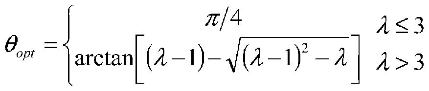
(2) arctan (λ - \) - ^{λ - \ )2 - λ > 3
[0019] In equation (2) λ represents the ratio between the OSNR in the 'good' polarisation state to the OSNR in the 'bad' polarisation state. This rotation angle is designed to minimise the bit error rate (BER) for a given OSNR difference between the two polarisation states. In practice, the value of λ may be
determined using OSNR information estimated at a corresponding receiver.
[0020] Interleaving is performed following angle rotation. In particular, the real parts of the rotated symbol values are input to digital-to-analog converters (DACs) 1 14, 1 16, while the imaginary parts are input to DACs 1 16, 120. The outputs of DACs 1 14, 1 16 comprise the in-phase (I) and quadrature (Q) components to be modulated onto a first polarisation state of the transmitted signal, while the
outputs of DACs 1 18, 120 comprise I and Q components of a signal to be modulated onto a second polarisation state of the transmitted signal.
[0021 ] A PDM optical signal source comprises an optical carrier source 122, a polarisation beam splitter 124, and a pair of l/Q (complex) modulators 126, 128. The I and Q components output from DACs 1 14, 1 16 are input to modulator 126, thereby modulating the first polarisation state of the optical carrier source 122. The outputs of DACs 1 18, 120 are input to modulator 128, thereby modulating the second polarisation state of the optical carrier 122. The modulated polarisation states are recombined in polarisation beam splitter 130, to produce the PDM optical signal which is transmitted through an optically-amplified transmission link 132.
[0022] The system 100 further comprises a receiver 133 which is configured to recover the transmitted information bits 102.
[0023] The transmitted PDM signal is detected, for example using a dual-polarisation coherent detector 134. The detector 134 may comprise, for example, a local oscillator laser source, a pair of optical hybrid circuits, and four pairs of balanced detectors, resulting in the detection of in-phase and quadrature components of the signals transmitted on the two polarisation states. The detected in-phase and quadrature components of the first polarisation state are input to analog-to-digital converters (ADCs) 136, 138, while the corresponding I and Q components of the second polarisation state are input to ADCs 140, 142. This results in four corresponding sequences of digitised samples, which are subject to front-end processing 144 within a digital signal processing (DSP) unit. The front-end DSP processes include front-end correction, clock recovery, channel impairment compensation and carrier recovery. The outputs from the front-end processing comprise a pair of equalised complex-valued sample sequences, i.e. real and imaginary parts corresponding with the I and Q components of the two received polarisation states respectively.
[0024] The equalised symbol values corresponding with the first polarisation state are input to OSNR estimation and scaling block 146, while the equalised symbol values corresponding with the second polarisation state are input to OSNR estimation and scaling block 148. In each of these DSP blocks the corresponding OSNR is estimated, for example using the statistical moments method as described by C Zhu et al, 'Statistical Moments Based OSNR
Monitoring for Coherent Optical Systems' Optics Express, Volume 20 No. 16, 1771 1 -17721 (2012). The equalised symbols are then rescaled differently, according to the estimated OSNR of each polarisation. In particular, the equalised symbols are multiplied by the square root of the estimated OSNR. In practice, the OSNR varies as a result of the stochastic nature of PDL, and therefore the OSNR estimation and rescaling should be updated periodically, in accordance with the associated state-of-polarisation rotation rate. Typically, a few thousand updates per second (i.e. kHz update rate) should be sufficient for transmission fibre having fast state-of-polarisation rotation.
[0025] The outputs of OSNR estimation and scaling blocks 146, 148 comprise real and imaginary parts of the corresponding rescaled and equalised symbols. The interleaving and data recovery are performed by inputting the real parts of the rescaled symbols to maximum likelihood detector (MLD) block 150, while the imaginary parts are input to MLD block 152. The MLD process applied for each symbol decision is described by the following equations:

D Re(ckeje )· JSNR, + ./' Jm(ckeje )- JSNR
[0026] In equation (3) Ck is the constellation alphabet (i.e. [1 +j, 1 -j, -1 +j, -1-j] for QPSK modulation) and Dk are the rotated and rescaled symbol values. The resulting decisions represent information bits that are recombined in multiplexer 154 in order to recover the output bit sequence 156. A bit error rate (BER) may
be determined by comparing the recovered output bits 156 with the original transmitted input bits 102.
[0027] As will be appreciated from the foregoing discussion, the presently disclosed embodiments of the invention are implemented substantially via digital signal processing. Such processing is performed both in the transmitter 101 and in the receiver 133. The various signal processing blocks shown in the exemplary embodiment 100 represent conceptual processing functions, which may be implemented, in practice, in a variety of different ways, as will be apparent to persons skilled in the art of signal processing. In practical implementations, for example, the digital processing may be implemented in software executing on a suitable central processing unit (e.g. a DSP device), or as a custom, or semi- custom, hardware unit, such as an application-specific integrated circuit (ASIC), or programmable hardware, such as a field programmable gate array (FPGA). Such implementations, and others relying on a combination of applicable digital processing components, all fall within the scope of the present invention.
[0028] Figure 2 is a schematic diagram showing the configuration 200 of a proof-of-concept experimental demonstration corresponding with the exemplary system of Figure 1 . Eight external cavity lasers (ECLs) 202, having a 50 GHz carrier spacing, are multiplexed with an 8x1 polarisation-maintaining (PM) coupler 204. The carrier waves are amplified using a polarisation-maintaining erbium- doped fibre amplifier (PM-EDFA) 206. An arbitrary waveform generator (AWG) 208 is used to generate baseband signals at 10 GSa/s, with either conventional PDM-QPSK, or polarisation pairwise coding QPSK (PPC-QPSK) embodying the invention. A pair of electrical amplifiers 210 is used to amplify the I and Q components of the signal generated by the AWG 208, which are then used to drive an optical l/Q modulator 212. The resulting modulated signals are amplified using a further PM-EDFA 214.
[0029] A PDM emulator 216 is used to delay the Ύ polarisation state of the optical signal with respect to the 'X' polarisation state. In the presently described proof-of-concept experiment, the delay was equivalent to 195 symbols, enabling
the single AWG 208 to be used to generate dual-polarisation signals. This is illustrated schematically by the blocks 228, which show that the desired PDM signals, suitable for decoding at the receiver, occupy alternate 195 symbol blocks.
[0030] The resulting optical signal is divided into its two polarisation states by polarisation beam splitter (PBS) 218. A frequency/channel-dependent PDL is generated using a Finisar WaveShaper (WS) 220, while a variable attenuator 222 is used to match the insertion loss of WS 220. The two polarisation states are recombined in PBC 224.
[0031 ] The resulting PDL-emulated signal is passed through a 50 GHz interleaver 226, and a further optical amplifier 230, before entering a recirculating loop 232. The recirculating loop 232 comprises two acousto-optic modulator (AOM) switches, 640 km of standard single-mode fibre, consisting of six 80 km spans and associated optical amplifiers, a gain-flattening WS, and a polarisation scrambler.
[0032] At the output of the recirculating loop 232, an ASE source 234 is used to add optical noise, e.g. to control the OSNR for single-channel back-to-back measurements. A further WS 236 is used to select the desired channel for coherent detection. The detection is performed by receiver 238, which generates four outputs (i.e. I and Q components of each of the X and Y polarisation states) which are sampled and digitised by a real-time oscilloscope 240. The resulting signals can be processed offline, in accordance with conventional PDM-QPSK processing techniques, or according to PPC-QPSK techniques embodying the invention.
[0033] Figure 3 shows a graph 300, comprising the spectrum of X and Y polarisation states of the WDM optical signal generated and transmitted into the recirculating loop 232 of the system 200 shown in Figure 2. The spectrum 300 shows wavelength on the horizontal axis 302, and corresponding power on the vertical axis 304. The higher-quality (Y) polarisation state is shown by the trace
306, while the lower-quality (X) polarisation state is shown by the trace 308.
According to conventional PDM transmission, it is expected that the overall performance of the system will be dominated by errors occurring in the lossy polarisation state represented by the spectrum 308.
[0034] Figure 4 shows a graph 400 of OSNR penalty as a function of PDL. In particular, PDL, in dB, is shown on the horizontal axis 402, and OSNR penalty for a BER of 10~3 is shown on the vertical axis 404. The BER is based on averaging across the two polarisation states. The measurements were performed for a single channel operating in back-to-back mode, i.e. without recirculation in the loop 232, and with added ASE generated by the source 234. Four curves are shown on the graph 400, namely experimental measurements for PDM-QPSK (406), experimental PPC-QPSK using an optimum rotation angle (408), experimental measurements for PPC-QPSK using a ττ/4 rotation (410), along with simulation results for worst-case (412) and best-case (414) PDM-QPSK.
[0035] As can be seen in the graph 400, the PDM-QPSK experimental results closely match the simulation results for worst case PDL, with a 3.5 dB OSNR penalty occurring for a PDL value of 7 dB. A PPC-QPSK signal, embodying the invention and using a ττ/4 rotation angle outperforms the PDM-QPSK signal significantly, show it just over 1 dB OSNR penalty with 7 dB PDL. Moreover, differences between the ττ/4 rotation angle and optimum angle, for PDL less than 7 dB, are not significant. This demonstrates that a fixed rotation angle can be used for all cases, thereby avoiding the need to feed back OSNR estimates from the receiver to the transmitter.
[0036] The best-case PDM-QPSK represented by the simulated results 414 corresponds with a 45-degree rotation between signal polarisation and the lossy axis, such that the OSNR penalty is distributed equally between the two polarisation states. These results show that a PPC-QPSK modulation method, embodying the invention, provides a substantial OSNR penalty benefit even as compared with this unrealistic best-case result.
[0037] Figure 5 shows a graph 500 of received signal quality factor for each of the eight WDM channels transmitted using the experimental configuration 200. The horizontal axis 502 shows channel index, while the vertical axis 504 shows quality factor, defined as:
Q1 (dB) = 201og10 [V2 erfc"' {2BER)\ (4)
[0038] Two curves are shown in the graph 500, namely experimental results for conventional PDM-QPSK (506), and for PPC-QPSK signals embodying the invention (508). As can be seen, the use of methods and apparatus embodying the invention, results in improvements in received signal quality for all channels in which PDL occurs. In the worst case, channel 1 with 7 dB PDL, a 2.5 dB improvement in quality factor is observed through the use of PPC-QPSK.
[0039] Figure 6 shows exemplary constellation diagrams 600 of a received signal embodying the invention. These constellation diagrams are, respectively: received signal in the X polarisation after equalisation (602); received signal in the Y polarisation after equalisation (604); the received signal in the X polarisation after rescaling (606); the received signal in the Y polarisation after rescaling (608); and the received signals following de-interleaving (610, 612). It is clearly apparent from the constellation diagrams 600 that, while the received signal in the X polarisation (in this case subjected to 6 dB PDL) is of significantly lower quality than the received signal in the Y polarisation, the processes of rescaling and de-interleaving, conducted according to the principles of the invention, effectively redistribute the optical noise between the two de-interleaved signals.
[0040] In summary, embodiments of the invention employ polarisation pairwise coding for PDM coherent optical signals, improving transmission performance in the presence of PDL. At the transmitter, the principles of rotating the original information symbols and interleaving the real and imaginary components between two polarisation states are employed. At the receiver, the detected X and Y polarisation signals are rescaled according to respective
OSNRs, and de-interleaved. As a result, the overall decoded signals extracted from the two polarisation states have similarly low error rates, and the overall performance is always superior to that of conventionally (non-pairwise-coded) PDM signals, which are dominated by high error rates in the poor quality polarisation state. An experimental proof-of-concept demonstration establishes that greatly enhanced overall system performance can be achieved, over a wide range of PDL, without any coding overhead, for single channel and WDM transmission systems.
[0041 ] While particular embodiments of the invention have been described in order to illustrate the principles of the invention, persons skilled in the art of optical communications will appreciate that these principles may be applied in a variety of different embodiments. For example, mapping methods other than QPSK may be employed, such as QAM, or other multi-level mapping techniques. The scope of the invention is therefore not limited to the described embodiments, but is as defined in the following claims.
Claims
1 . A method of transmitting digital information over an optical channel comprising:
mapping input digital information bits to first and second complex-valued symbol sets;
applying a complex rotation to each symbol of the first and second complex-valued symbol sets;
modulating in-phase (I) and quadrature (Q) components of a first polarisation state of an optical carrier with the real parts of the first and second complex-valued symbol sets respectively; and
modulating in-phase (I) and quadrature(Q) components of a second polarisation state of the optical carrier with the imaginary parts of the first and second complex-valued symbol sets respectively.
2. The method of claim 1 wherein the complex rotation comprises a ττ/4 rotation angle.
3. The method of claim 1 wherein the complex rotation comprises an optical angle 9opt defined by:

4. A method of recovering digital information modulated onto first and second polarisation states of an optical carrier and transmitted over an optical channel, the method comprising:
receiving a first complex-valued symbol set wherein the real and imaginary parts of each symbol comprise equalised samples of respective in-phase (I) and quadrature (Q) components of a signal modulated onto the first polarisation state of the optical carrier;
receiving a second complex-valued symbol set wherein the real and imaginary parts of each symbol comprise equalised samples of respective in- phase (I) and quadrature (Q) components of a signal modulated onto the second polarisation state of the optical carrier;
computing, from the first complex-valued symbol set, a first estimated optical signal-to-noise ratio (OSNR) value of the signal modulated onto the first polarisation state of the optical carrier and, from the second complex-valued symbol set, a second estimated OSNR value of the signal modulated onto the second polarisation state of the optical carrier;
scaling symbols of the first and second complex-valued symbol sets according to the first and second estimated OSNR values to generate respective first and second scaled symbol sets; and
recovering a first sequence of digital information bits from the real parts of the first and second scaled symbol sets, and a second sequence of digital information bits from the imaginary parts of the first and second scaled symbol sets.
5. The method of claim 4 wherein scaling of the first and second complex- valued symbol sets comprises multiplication by the square root of the first and second estimated OSNR values, respectively.
6. The method of claim 4 further comprising updating the first and second OSNR values at time intervals determined in accordance with a rate of change of a state of polarisation of the received optical signal.
7. The method of claim 6 wherein the time intervals at which OSNR values are updated are between one microsecond and one millisecond.
8. The method of claim 4 wherein recovering the first sequence of digital information bits comprises performing maximum likelihood detection based upon the real parts of the first and second scaled symbol sets, and recovering the second sequence of digital information bits comprises performing maximum likelihood detection based on the imaginary parts of the first and second scaled symbol sets.
9. An optical transmitter comprising:
a digital processor configured to:
map input digital information bits to first and second complex-valued symbol sets;
apply a complex rotation to each symbol of the first and second complex-valued symbol sets to generate corresponding first and second rotated symbol sets; and
output real and imaginary parts of the first and second rotated symbol sets,
a digital-to-analog conversion (DAC) unit, operatively coupled to the digital processor, configured to receive the real part of the first rotated symbol set, the imaginary part of the first rotated symbol set, the real part of the second rotated symbol set, and the imaginary part of the second rotated symbol set, respectively, and to generate corresponding first, second, third and fourth electrical signals; and
an optical carrier source having first and second polarisation states, coupled to first and second modulation units, the first modulation unit being configured to modulate in-phase (I) and quadrature (Q) components of the first polarisation state of the optical source with the first and third electrical signals, respectively, and the second modulation unit being configured to modulate in- phase (I) and quadrature (Q) components of the second polarisation state with the second and fourth electrical signals, respectively.
10. The transmitter of claim 9 wherein the digital processor is configured to apply the complex rotation comprising a ττ/4 rotation angle.
1 1 . The transmitter of claim 9 wherein the digital processor is further configured to compute an optimum complex rotation angle 6opt defined by:
12. An optical receiver, configured to recover digital information modulated onto first and second polarisation states of an optical carrier and transmitted over an optical channel, the receiver comprising a digital processor configured to: receive a first complex-valued symbol set wherein the real and imaginary parts of each symbol comprise equalised samples of respective in-phase (I) and quadrature (Q) components of a signal modulated onto the first polarisation state of the optical carrier;
receive a second complex-valued symbol set wherein the real and imaginary parts of each symbol comprise equalised samples of respective in- phase (I) and quadrature (Q) components of a signal modulated onto the second polarisation state of the optical carrier;
compute, from the first complex-valued symbol set, a first estimated optical signal-to-noise ratio (OSNR) value of the signal modulated onto the first polarisation state of the optical carrier and, from the second complex-valued symbol set, a second estimated OSNR value of the signal modulated onto the second polarisation state of the optical carrier;
scale symbols of the first and second complex-valued symbol sets according to the first and second estimated OSNR values to generate respective first and second scaled symbol sets; and
recover a first sequence of digital information bits from the real parts of the first and second scaled symbol sets, and a second sequence of digital information bits from the imaginary parts of the first and second scaled symbol sets.
13. The optical receiver of claim 12 wherein scaling of the first and second complex-valued symbol sets comprises multiplication by the square root of the first and second estimated OSNR values, respectively.
14. The optical receiver of claim 12 wherein the digital processor is further configured to update the first and second estimated OSNR values at time intervals determined in accordance with a rate of change of a state of polarisation of the received optical signal.
15. A method of transmitting digital information comprising:
mapping input digital information bits to first and second complex-valued symbol sets;
applying a complex rotation to each symbol of the first and second complex-valued symbol sets;
modulating in-phase (I) and quadrature (Q) components of a first polarisation state of an optical carrier with the real parts of the first and second complex valued symbol sets respectively;
modulating in-phase (I) and quadrature(Q) components of a second polarisation state of the optical carrier with the imaginary parts of the first and second complex-valued symbol sets respectively;
transmitting the modulated optical carrier over an optical channel;
detecting the modulated optical carrier at a receiving end of the optical channel to obtain electrical signals corresponding with received in-phase (I) and quadrature (Q) components of the first and second polarisation states;
performing digitisation and equalisation of the electrical signals to generate first and second complex-valued symbol sets, wherein real and imaginary parts of each symbol of the first complex-valued symbol set comprise equalised samples of the I and Q components of the first polarisation state, and real and imaginary
parts of each symbol of the second complex-valued symbol set comprise equalised samples of the I and Q components of the second polarisation state; computing, from the first complex-valued symbol set, a first estimated optical signal-to-noise ratio (OSNR) value of the signal modulated onto the first polarisation state of the optical carrier and, from the second complex-valued symbol set, a second estimated OSNR value of the signal modulated onto the second polarisation state of the optical carrier;
scaling symbols of the first and second complex-valued symbol sets according to the first and second estimated OSNR values to generate respective first and second scaled symbol sets; and
recovering a first sequence of digital information bits from the real parts of the first and second scaled symbol sets, and a second sequence of digital information bits from the imaginary parts of the first and second scaled symbol sets.
Applications Claiming Priority (2)
| Application Number | Priority Date | Filing Date | Title |
|---|---|---|---|
| AU2015900977 | 2015-03-18 | ||
| AU2015900977A AU2015900977A0 (en) | 2015-03-18 | Method and system for polarisation division multiplexed optical transmission |
Publications (1)
| Publication Number | Publication Date |
|---|---|
| WO2016145493A1 true WO2016145493A1 (en) | 2016-09-22 |
Family
ID=56918171
Family Applications (1)
| Application Number | Title | Priority Date | Filing Date |
|---|---|---|---|
| PCT/AU2016/050192 Ceased WO2016145493A1 (en) | 2015-03-18 | 2016-03-18 | Method and system for polarisation division multiplexed optical transmission |
Country Status (1)
| Country | Link |
|---|---|
| WO (1) | WO2016145493A1 (en) |
Cited By (4)
| Publication number | Priority date | Publication date | Assignee | Title |
|---|---|---|---|---|
| WO2023021260A1 (en) * | 2021-08-20 | 2023-02-23 | Mimopt Technology | I/q coding method for wdm communication system over optical fibre |
| WO2023187299A1 (en) * | 2022-04-01 | 2023-10-05 | Mimopt Technology | Dense i/q coding method and device for a fiber-optic wdm communication system |
| WO2023187300A1 (en) * | 2022-04-01 | 2023-10-05 | Mimopt Technology | Dense i/q coding method and device for a fiber-optic sdm communication system |
| EP4412117A4 (en) * | 2021-12-02 | 2025-01-22 | Huawei Technologies Co., Ltd. | COMMUNICATION METHOD AND APPARATUS |
Citations (5)
| Publication number | Priority date | Publication date | Assignee | Title |
|---|---|---|---|---|
| KR20100065034A (en) * | 2008-12-05 | 2010-06-15 | 한국전자통신연구원 | System for visible light communications with multi-carrier modulation and method thereof |
| KR20110139931A (en) * | 2010-06-24 | 2011-12-30 | 충북대학교 산학협력단 | Visible light transmitting device, visible light receiving device and visible light communication system including the same |
| US20130034174A1 (en) * | 2010-10-16 | 2013-02-07 | Zte Corporation | Method, device and system for complex carrier modulation |
| US20130034193A1 (en) * | 2010-10-16 | 2013-02-07 | Zte Corporation | method and device for demodulating complex carriers |
| WO2013039968A1 (en) * | 2011-09-16 | 2013-03-21 | Alcatel Lucent | Performance enhancement through optical variants |
-
2016
- 2016-03-18 WO PCT/AU2016/050192 patent/WO2016145493A1/en not_active Ceased
Patent Citations (5)
| Publication number | Priority date | Publication date | Assignee | Title |
|---|---|---|---|---|
| KR20100065034A (en) * | 2008-12-05 | 2010-06-15 | 한국전자통신연구원 | System for visible light communications with multi-carrier modulation and method thereof |
| KR20110139931A (en) * | 2010-06-24 | 2011-12-30 | 충북대학교 산학협력단 | Visible light transmitting device, visible light receiving device and visible light communication system including the same |
| US20130034174A1 (en) * | 2010-10-16 | 2013-02-07 | Zte Corporation | Method, device and system for complex carrier modulation |
| US20130034193A1 (en) * | 2010-10-16 | 2013-02-07 | Zte Corporation | method and device for demodulating complex carriers |
| WO2013039968A1 (en) * | 2011-09-16 | 2013-03-21 | Alcatel Lucent | Performance enhancement through optical variants |
Cited By (10)
| Publication number | Priority date | Publication date | Assignee | Title |
|---|---|---|---|---|
| WO2023021260A1 (en) * | 2021-08-20 | 2023-02-23 | Mimopt Technology | I/q coding method for wdm communication system over optical fibre |
| FR3126274A1 (en) * | 2021-08-20 | 2023-02-24 | Mimopt Technology | IQ CODING METHOD FOR WDM FIBER OPTIC COMMUNICATION SYSTEM |
| JP2024530267A (en) * | 2021-08-20 | 2024-08-16 | ミモプト・テクノロジー | I/Q coding method for a WDM communication system over optical fiber - Patents.com |
| US12587302B2 (en) * | 2021-08-20 | 2026-03-24 | Mimopt Technology | I/Q coding method for WDM communication system over optical fibre |
| EP4412117A4 (en) * | 2021-12-02 | 2025-01-22 | Huawei Technologies Co., Ltd. | COMMUNICATION METHOD AND APPARATUS |
| US12609859B2 (en) | 2021-12-02 | 2026-04-21 | Huawei Technologies Co., Ltd. | Communication method and apparatus |
| WO2023187299A1 (en) * | 2022-04-01 | 2023-10-05 | Mimopt Technology | Dense i/q coding method and device for a fiber-optic wdm communication system |
| WO2023187300A1 (en) * | 2022-04-01 | 2023-10-05 | Mimopt Technology | Dense i/q coding method and device for a fiber-optic sdm communication system |
| FR3134266A1 (en) * | 2022-04-01 | 2023-10-06 | Mimopt Technology | DENSE IQ CODING METHOD AND DEVICE FOR WDM COMMUNICATION SYSTEM ON OPTICAL FIBER |
| FR3134267A1 (en) * | 2022-04-01 | 2023-10-06 | Mimopt Technology | DENSE IQ CODING METHOD AND DEVICE FOR SDM COMMUNICATION SYSTEM ON OPTICAL FIBER |
Similar Documents
| Publication | Publication Date | Title |
|---|---|---|
| Qian et al. | High capacity/spectral efficiency 101.7-Tb/s WDM transmission using PDM-128QAM-OFDM over 165-km SSMF within C-and L-bands | |
| EP2672638B1 (en) | Methods and apparatus for pre and post equalization in optical communications systems | |
| Buchali et al. | Optical OFDM: A promising high‐speed optical transport technology | |
| US9882652B2 (en) | Methods and systems for optical detection | |
| Li et al. | Spectrally efficient 168 Gb/s/λ WDM 64-QAM single-sideband nyquist-subcarrier modulation with Kramers–Kronig direct-detection receivers | |
| US9590833B2 (en) | Reception of 2-subcarriers coherent orthogonal frequency division multiplexed signals | |
| Nopchinda et al. | Dual polarization coherent optical spectrally efficient frequency division multiplexing | |
| EP2852076A1 (en) | Non-linear distortion compensator, method of compensating non-linear distortion, and communication apparatus | |
| Zhang et al. | 400 G transmission of super-Nyquist-filtered signal based on single-carrier 110-GBaud PDM QPSK with 100-GHz grid | |
| Li et al. | Digital linearization of direct-detection transceivers for spectrally efficient 100 Gb/s/λ WDM metro networking | |
| Xu et al. | Field trial over 820 km installed SSMF and its potential Terabit/s superchannel application with up to 57.5-Gbaud DP-QPSK transmission | |
| Rezania et al. | Transmission performance of 448 Gb/s single-carrier and 1.2 Tb/s three-carrier superchannel using dual-polarization 16-QAM with fixed LUT based MAP detection | |
| WO2016145493A1 (en) | Method and system for polarisation division multiplexed optical transmission | |
| Ferreira et al. | Demonstration of Nyquist UDWDM-PON with digital signal processing in real-time | |
| Li et al. | 192-Gb/s 160-km transmission of carrier-assisted dual-polarization signal with Stokes vector direct detection | |
| EP2936707B1 (en) | Communication system for a nonlinear fiber channel | |
| WO2012139165A2 (en) | Joint coding for optical ofdm | |
| Li et al. | Performance implications of cascaded wavelength selective switches on a probabilistically shaped 64-QAM system | |
| Wang et al. | Transmission performance comparison of 128-SP-QAM and PM-16QAM in a WDM system | |
| Raybon et al. | Single-carrier and dual-carrier 400-Gb/s and 1.0-Tb/s transmission systems | |
| Yang et al. | Modulation format independent blind polarization demultiplexing algorithms for elastic optical networks | |
| Zhu et al. | 4× 200Gb/s Twin-SSB Nyquist subcarrier modulation WDM transmission over 160km SSMF with direct detection | |
| He et al. | Flexible multi-dimensional modulation method for elastic optical networks | |
| Omomukuyo et al. | Discrete frft-based frame and frequency synchronization for coherent optical systems | |
| de Jauregui Ruiz | Advanced modulation formats and nonlinear mitigation for spectral efficient optical transmission systems |
Legal Events
| Date | Code | Title | Description |
|---|---|---|---|
| 121 | Ep: the epo has been informed by wipo that ep was designated in this application |
Ref document number: 16764069 Country of ref document: EP Kind code of ref document: A1 |
|
| NENP | Non-entry into the national phase |
Ref country code: DE |
|
| 122 | Ep: pct application non-entry in european phase |
Ref document number: 16764069 Country of ref document: EP Kind code of ref document: A1 |