WO2016035722A1 - 発光材料及びこれを用いた表示装置。 - Google Patents
発光材料及びこれを用いた表示装置。 Download PDFInfo
- Publication number
- WO2016035722A1 WO2016035722A1 PCT/JP2015/074547 JP2015074547W WO2016035722A1 WO 2016035722 A1 WO2016035722 A1 WO 2016035722A1 JP 2015074547 W JP2015074547 W JP 2015074547W WO 2016035722 A1 WO2016035722 A1 WO 2016035722A1
- Authority
- WO
- WIPO (PCT)
- Prior art keywords
- dna
- display device
- luminescent material
- lipid compound
- luminescent
- Prior art date
- Legal status (The legal status is an assumption and is not a legal conclusion. Google has not performed a legal analysis and makes no representation as to the accuracy of the status listed.)
- Ceased
Links
Images


Classifications
-
- C—CHEMISTRY; METALLURGY
- C09—DYES; PAINTS; POLISHES; NATURAL RESINS; ADHESIVES; COMPOSITIONS NOT OTHERWISE PROVIDED FOR; APPLICATIONS OF MATERIALS NOT OTHERWISE PROVIDED FOR
- C09K—MATERIALS FOR MISCELLANEOUS APPLICATIONS, NOT PROVIDED FOR ELSEWHERE
- C09K11/00—Luminescent materials, e.g. electroluminescent or chemiluminescent
- C09K11/06—Luminescent materials, e.g. electroluminescent or chemiluminescent containing organic luminescent materials
-
- C—CHEMISTRY; METALLURGY
- C09—DYES; PAINTS; POLISHES; NATURAL RESINS; ADHESIVES; COMPOSITIONS NOT OTHERWISE PROVIDED FOR; APPLICATIONS OF MATERIALS NOT OTHERWISE PROVIDED FOR
- C09K—MATERIALS FOR MISCELLANEOUS APPLICATIONS, NOT PROVIDED FOR ELSEWHERE
- C09K11/00—Luminescent materials, e.g. electroluminescent or chemiluminescent
- C09K11/08—Luminescent materials, e.g. electroluminescent or chemiluminescent containing inorganic luminescent materials
Definitions
- the present invention relates to a light emitting material and a display device using the same.
- Display devices for displaying information such as televisions, personal computer monitors and mobile phone displays are indispensable devices in the information-oriented society in recent years.
- a display device has a large number of pixels arranged in a plane, and can be displayed as an image by adjusting the color, brightness, and the like of each pixel.
- a light emitting material is disposed between a pair of substrates on which electrodes are arranged for each region corresponding to a pixel, and a voltage is applied to the electrodes to cause the light emitting material to emit light, thereby performing display.
- ECL display device that is going to be.
- Patent Documents 1 and 2 describe attempts to impart light polarization to the light emitted from the display device.
- the anisotropy of circularly polarized light emission is increased by bonding a molecule having another ligand to a light-emitting rare earth complex having a chiral ligand, thereby changing the structure of the whole complex. Techniques to do this are disclosed.
- Patent Document 2 discloses a technique for generating circularly polarized light by combining deoxyribonucleic acid (hereinafter referred to as “DNA”), a lipid compound having a cationic functional group, and a luminescent material.
- DNA deoxyribonucleic acid
- Patent Document 1 a complicated molecular design, a multi-step synthesis process, and a purification process are required to increase the circularly polarized light intensity, and much cost and time are required to synthesize an amount that can be used as a luminescent material.
- the solvent and polymer species that dissolve or disperse the light-emitting rare earth complex are greatly limited.
- the circular polarization may be lost.
- Patent Document 2 since a lipid compound having a cationic functional group is used, there remains a problem in the stability of the material.
- an object of the present invention is to provide a light emitting material containing DNA having a more stable structure and a display device using the light emitting material.
- a luminescent material according to one aspect of the present invention that solves the above problems includes deoxyribonucleic acid, a lipid compound that electrostatically binds to a phosphate group of deoxyribonucleic acid, and a luminescent substance. .
- the lipid compound in the luminescent material preferably contains a quaternary ammonium salt having 10 or more carbon atoms, although not limited thereto.
- the light-emitting material preferably has a weight of deoxyribonucleic acid and lipid compound in the range of 1 to less than 10 when the weight of the light-emitting substance is 1.
- a display device is a display device including a pair of substrates and a light-emitting material sandwiched between the pair of substrates.
- the light-emitting material includes deoxyribonucleic acid and deoxyribonucleic acid. It contains a lipid compound that electrostatically binds to a phosphate group of a nucleic acid, and a luminescent substance.
- the lipid compound in the light emitting material preferably contains a quaternary ammonium salt having 10 or more carbon atoms.
- the light-emitting material preferably has a weight of deoxyribonucleic acid and lipid compound in the range of 1 to less than 10 when the weight of the light-emitting substance is 1.
- FIG. 1 is a schematic view relating to a cross section of a display device (hereinafter referred to as “the present device”) 1 according to the present embodiment.
- the device 1 includes a pair of substrates 2 and 3 on which electrodes 21 and 31 are formed, respectively, and a light emitting material 4 sandwiched between the pair of substrates 21 and 31. Configured.
- the pair of substrates 2 and 3 are used to sandwich and hold the light emitting material 4, and at least one of the substrates 2 and 3 may be transparent.
- Type display device can be realized.
- the materials of the substrates 2 and 3 are not limited as long as they have a certain degree of hardness and chemical stability and can stably hold the material layer, but glass, plastic, metal A semiconductor or the like can be used, and glass or plastic can be used when used as a transparent substrate.
- the electrodes 21 and 31 are formed on each of the pair of substrates 2 and 3 on the opposite surface side (inside) as described above.
- This electrode is used to apply a voltage to the material layer sandwiched between the pair of electrodes 2 and 3.
- the material of the electrode is not limited as long as it has suitable conductivity.
- a transparent electrode such as ITO or IZO is preferable.
- the electrode according to the present embodiment may be formed on the substrate in a shape that matches a pattern such as a character to be displayed, or an electrode pattern divided into a plurality of the same regions is formed side by side on a plurality of substrates. It may be what you did. When divided into a plurality of areas, each area is regarded as a pixel, and there is an advantage that display can be controlled for each pixel and display of complicated shapes can be handled.
- the distance between the electrodes is not limited as long as a voltage can be applied between the electrodes and the light emitting material can emit light, but it can be 1 ⁇ m or more and 10 mm or less, and preferably 1 ⁇ m or more and 1 mm or less. It is.
- the electrodes according to the present embodiment are connected to a power source via conductive wires, respectively, and voltage application to and release from the material layer can be controlled by turning the power source on and off.
- the voltage intensity at the time of voltage application can be appropriately adjusted depending on the distance between the pair of substrates, and is not limited.
- the voltage intensity is 1.0 ⁇ 10 4 V / m or more and 1.0 ⁇ 10 6. It is preferable to be within the range of V / m or less.
- the light emitting material 4 is a material containing a component that emits light when a voltage is applied as described above, and electrostatically binds to at least deoxyribonucleic acid (DNA) and a phosphate group of deoxyribonucleic acid.
- DNA deoxyribonucleic acid
- a lipid compound and a luminescent substance are examples of lipid compounds.
- DNA has a structure with a double helix structure. Specifically, two polynucleotide strands are arranged in parallel, and each has a helical structure bonded by complementary base pair hydrogen bonding.
- the DNA in the present embodiment is not particularly limited as long as it has a phosphate group and can form a double helix structure, and the DNA base sequence is not particularly limited.
- the light emitting material 4 includes a lipid compound in addition to the DNA.
- the lipid compound is not particularly limited as long as it is poorly soluble in water and can be electrostatically bound to the phosphate group of DNA.
- the lipid compound is aliphatic or aromatic. It is preferable that it is provided with a group hydrocarbon group, and more preferably it has 10 or more carbon atoms.
- the lipid compound preferably has a cationic functional group for electrostatic bonding with a phosphate group, and preferably has a quaternary ammonium group, for example.
- the light emitting material 4 includes a light emitting substance.
- the luminescent substance is not limited as long as it can emit light as described above, but is preferably at least one of a luminescent molecule or a luminescent metal complex, for example.
- Examples of the light-emitting metal complex include, but are not limited to, ruthenium complex, iridium complex, rhodium complex, osmium complex, platinum complex, rhenium complex, zinc complex, aluminum complex, rubidium complex, and Ln. It is preferably at least one of rare earth complexes.
- Ln is neodymium (Nd), samarium (Sm), europium (Eu), terbium (Tb), ytterbium (Yb), praseodymium (Pr), cerium (Ce), dysprosium (Dy), An ion of either erbium (Er) or thulium (Tm) is preferable.
- the light emitting material includes a solvent for uniformly dissolving or dispersing each of the above substances.
- the solvent is not limited as long as it has the above function, but an aqueous or alcohol solvent is preferably used.
- concentration of the said luminescent substance with respect to a solvent For example, it is preferable that they are 1 mM or more and 5 M or less.
- This device can emit light by colliding an electrochemically purified oxidant and a reductant by applying a voltage between the electrodes.
- this apparatus can obtain electrochemiluminescence even at high frequencies.
- the light emitting material may be used as, for example, a modification material for electrodes disposed on a pair of substrates.
- a modification material for electrodes disposed on a pair of substrates For example, it can also be realized by applying a solution containing DNA on the electrodes, introducing a lipid compound and a luminescent substance to produce a modified electrode, and placing an electrolytic solution between the electrodes.
- the present invention it is possible to provide a light emitting material containing DNA having a more stable structure and a display device using the light emitting material. More specifically, in the present invention, light emission can be enhanced by a very simple technique by combining DNA, a lipid compound, and a light emitting material. In this system, the intensity of circularly polarized light emitted from the light emitting molecule or the light emitting metal complex is also dramatically increased. In the conventional technique, for example, the technique described in Patent Document 1 above, there remains a problem that a precise molecular design and a complicated organic synthesis process are required to increase the circularly polarized light intensity.
- the light emission intensity and the circularly polarized light emission intensity can be significantly increased by a very simple method such as mixing a functional molecule or a light-emitting metal complex with a DNA composite material.
- the solvent used at this time is aqueous or alcoholic, it is possible to produce a material with a low cost and a small environmental burden with a low environmental load.
- the DNA composite material can be formed into a film in this state, there is almost no possibility of loss of circularly polarized light emission due to the kind of matrix as seen in the conventional invention, and it can be applied to various devices. It will be easier.
- a display device is constructed using the modified electrode made of the composite material obtained in the present invention, the light emission response to changes in the voltage applied to the element is significantly improved.
- the display device according to the present invention requires the presence of ionic substances on the basis of its driving principle, and the flatness and uniformity of the film. Can be driven even if it is not so high.
- composite DNA-CTMA / Eu (III) (D-facam) 3 solution
- the anisotropy factor (g value) indicating the high circularly polarized light emission in the 590 nm emission band increases from about 0.3 to 0.75. Since the g value of the CPL spectrum of a general optically active organic molecule is about 0.001, and the g value of an optically active rare earth complex is about 0.1 to 0.5, the DNA composite material obtained in this example It can be seen that the circular polarization characteristics of are very high.
- Example 2 A 5 mmol / L DNA aqueous solution was cast on an ITO substrate to prepare a DNA film having a thickness of about 0.5 ⁇ m, and introduced into a 10 mmol / L Ru (bpy) 3 Cl 2 aqueous solution. A potential of 5 V (Ag / Ag + ) was applied to introduce Ru (bpy) 3 2+ into the membrane. Cyclic voltammetry (CV) measurement and absorption spectrum measurement were performed on the prepared composite membrane. As a result, the prepared composite membrane showed absorption based on ML (CT) of Ru (bpy) 3 2+ , and it was found that the Ru (II) complex was introduced into the DNA membrane. Further, in the CV measurement, redox behavior due to Ru (bpy) 32+ was observed, and it was revealed that the Ru (II) complex in the film was electrochemically active.
- CT ML
- the measurement of the electrochemiluminescence characteristics shows the luminescence intensity-frequency characteristics when a ⁇ 4 V rectangular wave AC voltage is applied between the electrodes of the display device and the applied frequency is swept from a high frequency to a low frequency.
- a display device in which the above Ru (bpy) 3 Cl 2 aqueous solution was sandwiched between normal ITO electrodes was manufactured and used.
- the present invention has industrial applicability as a display device and a light emitting material used therefor.
Landscapes
- Chemical & Material Sciences (AREA)
- Engineering & Computer Science (AREA)
- Materials Engineering (AREA)
- Organic Chemistry (AREA)
- Inorganic Chemistry (AREA)
- Electroluminescent Light Sources (AREA)
Abstract
より安定した構造のDNAを含む発光材料、これを用いた表示装置を提供する。そのため、本発明の一の観点に係る発光材料は、デオキシリボ核酸と、デオキシリボ核酸のリン酸基に静電的に結合する脂質化合物と、発光性物質と、を含むことを特徴とする。また本観点において、限定されるわけではないが発光材料における脂質化合物は、炭素数が10以上の四級アンモニウム塩を含むことが好ましい。また本観点において、限定されるわけではないが発光材料において、発光性物質の重量を1とした場合に、デオキシリボ核酸及び脂質化合物の重量が1以上10未満の範囲内にあることが好ましい。また、本発明の他の一観点に係る表示装置は、一対の基板と、一対の基板の間に挟持される発光材料と、を備える表示装置であって、発光材料は、デオキシリボ核酸と、デオキシリボ核酸のリン酸基に静電的に結合する脂質化合物と、発光性物質と、を含むことを特徴とする。
Description
本発明は、発光材料及びこれを用いた表示装置に関する。
テレビやパソコンモニタ、携帯電話のディスプレイを始めとした情報を表示するための装置(表示装置)は、近年の情報化社会において欠かすことのできない装置である。
表示装置は一般に、多数の画素を平面的に配置しており、この各画素における色、明るさ等をそれぞれ調整することで画像として表示することができる。この表示装置の一例として、画素に対応する領域ごとに電極が配置された一対の基板の間に発光材料を配置し、この電極に電圧を引加することで発光材料を発光させ、表示を行おうとするECL表示装置がある。
一方近年、表示装置から発せられる光自体に偏光性を持たせようとする試みがなされてきている。表示装置から発せられる光自体に偏光性を持たせることで、例えば使用者に立体感を感じさせるいわゆる3D表示、商品等の偽造を検出するための識別マーク等への応用が期待できる。
表示装置から発せられる光自体に偏光性を持たせようとする試みに関しては、例えば下記特許文献1、2に記載がある。下記特許文献1には、キラルな配位子を有する発光性希土類錯体に別の配位子を有する分子を結合させることによって、錯体全体の構造を変化させて円偏光発光の異方性を大きくする技術が開示されている。また下記特許文献2には、デオキシリボ核酸(以下「DNA」という。)とカチオン性官能基を備える脂質化合物と、発光材料を組み合わせて円偏光を発生させようとする技術が開示されている。
しかしながら、上記特許文献1では、円偏光強度を高めるために複雑な分子設計や多段階の合成過程、精製過程が必要で、発光材料として使用できる量を合成するのに多くのコストと時間を要するといった課題がある。またこの技術では発光性希土類錯体を溶解又は分散させる溶媒・ポリマー種に大きな制限をうけており、場合によっては円偏光性が失われてしまう場合もあるため、溶媒等の同時に使用する材料の選択に大きな制限を受けてしまうといった課題がある。
また、上記特許文献2では、カチオン性官能基を備える脂質化合物を用いるものであるため、材料の安定性において課題が残る。
そこで、本発明は、上記課題を鑑み、より安定した構造のDNAを含む発光材料、これを用いた表示装置を提供することを目的とする。
上記課題を解決する本発明の一の観点に係る発光材料は、デオキシリボ核酸と、デオキシリボ核酸のリン酸基に静電的に結合する脂質化合物と、発光性物質と、を含むことを特徴とする。
また本観点において、限定されるわけではないが発光材料における脂質化合物は、炭素数が10以上の四級アンモニウム塩を含むことが好ましい。
また本観点において、限定されるわけではないが発光材料において、発光性物質の重量を1とした場合に、デオキシリボ核酸及び脂質化合物の重量が1以上10未満の範囲内にあることが好ましい。
また、本発明の他の一観点に係る表示装置は、一対の基板と、一対の基板の間に挟持される発光材料と、を備える表示装置であって、発光材料は、デオキシリボ核酸と、デオキシリボ核酸のリン酸基に静電的に結合する脂質化合物と、発光性物質と、を含むことを特徴とする。
また、本観点において、限定されるわけではないが、発光材料における脂質化合物は、炭素数が10以上の四級アンモニウム塩を含むことが好ましい。
また本観点において、限定されるわけではないが発光材料において、発光性物質の重量を1とした場合に、デオキシリボ核酸及び脂質化合物の重量が1以上10未満の範囲内にあることが好ましい。
以上、本発明により、より安定した構造のDNAを含む発光材料、これを用いた表示装置を提供することができる。
以下、本発明の実施形態について、図面を用いて詳細に説明する。ただし、本発明は多くの異なる形態による実施が可能であり、以下に示す実施形態、実施例の例示に限定されるものではない。
図1は、本実施形態に係る表示装置(以下「本装置」という。)1の断面に関する概略図である。本図で示すように、本装置1は、それぞれにおいて電極21、31が形成された一対の基板2、3と、この一対の基板21、31の間に挟持された発光材料4と、を有して構成されている。
本実施形態において一対の基板2、3は、発光材料4を挟み保持するために用いられるものであって、基板2、3の少なくとも一方が透明であればよいが、双方透明であれば、透過型の表示装置を実現することができる。本実施形態では説明のため双方透明な場合で説明する。なお、基板2、3の材料としては、ある程度の硬さ、化学的安定性を有し、安定的に材料層を保持することができる限りにおいて限定されるわけではないが、ガラス、プラスチック、金属、半導体等を採用することができ、透明な基板として用いる場合はガラスやプラスチックを用いることができる。
また本実施形態において、一対の基板2、3のそれぞれには、対向する面側(内側)に、上記のとおり電極21、31が形成されている。この電極は一対の電極2、3によって挟持される材料層に電圧を印加するために用いられるものである。電極の材料としては、好適な導電性を有する限りにおいて限定されるわけではないが、例えば基板2、3の材質が透明な基板である場合はITOやIZO等の透明電極であることが好ましい。
また本実施形態に係る電極は、基板上に、表示したい文字などのパターンにあわせた形状として形成してもよく、また、同じ複数の領域毎に区分された電極パターンを複数基板上に並べて形成したものであってもよい。複数の領域毎に区分すると、この各領域を画素とし、画素毎に表示を制御し、複雑な形状の表示にも対応できるといった利点がある。
電極間の距離としては、電極間に電圧を印加し、発光材料を発光させることができる限りにおいて限定されるわけではないが、1μm以上10mm以下が可能であり、望ましくは1μm以上1mm以下の範囲である。
なお本実施形態に係る電極は、それぞれ導電性を有する配線を介して電源に接続されており、この電源のON、OFFにより材料層に電圧の印加、印加の解除を制御することができる。なお電圧印加の際の電圧の強度としては、一対の基板間の距離によって適宜調整が可能であり限定されるわけではないが、例えば1.0×10⁴V/m以上1.0×106V/m以下の範囲内であることが好ましい。
また本実施形態に係る発光材料4は、上記のとおり電圧の印加によって発光する成分を含む材料であって、少なくとも、デオキシリボ核酸(DNA)と、デオキシリボ核酸のリン酸基に静電的に結合する脂質化合物と、発光性物質と、を含む。
本実施形態において、DNAは、二重らせん構造を備えた構造となっている。具体的には、二本のポリヌクレオチド鎖が平行して配置され、それぞれ相補的な塩基対の水素結合によって結合し、らせん構造を備えたものである。本実施形態におけるDNAは、リン酸基を備えて二重らせん構造を構成することができる限りにおいて特段の制限はなく、DNAの塩基配列に特段の制限はない。
また本実施形態に係る発光材料4は、上記DNAのほか、脂質化合物を含む。脂質化合物は、水に対する難溶性を備えるものであって、DNAのリン酸基と静電的に結合することのできるものであれば特に限定されるわけではないが、好ましくは、脂肪族又は芳香族の炭化水素基を備えたものであることが好ましく、より好ましくは炭素数が10以上であることが好ましい。さらに、脂質化合物は、上記のとおり、リン酸基と静電的に結合するためにカチオン性官能基を備えていることが好ましく、例えば四級アンモニウム基を備えたものであることが好ましい。
また本実施形態に係る発光材料4は、発光性物質を備えている。発光物質としては、上記のとおり発光することができる限りにおいて限定されるわけではないが、例えば発光性分子又は発光性金属錯体の少なくともいずれかであることが好ましい。
発光性金属錯体としては、限定されるわけではないが、例えば、ルテニウム錯体、イリジウム錯体、ロジウム錯体、オスミウム錯体、白金錯体、レニウム錯体、亜鉛錯体、アルミニウム錯体、ルビジウム錯体、及びLnで記載される希土類錯体の少なくともいずれかであることが好ましい。なお、希土類錯体の場合、Lnは、ネオジム(Nd)、サマリウム(Sm)、ユウロピウム(Eu)、テルビウム(Tb)、イッテルビウム(Yb)、プラセオジム(Pr)、セリウム(Ce)、ジスプロシウム(Dy)、エルビウム(Er)、ツリウム(Tm)のいずれかのイオンであることが好ましい。
また、本実施形態において、発光材料は、上記各物質を均一に溶解又は分散させるための溶媒を備えている。溶媒としては上記の機能を有する限りにおいて限定されるわけではないが水系又はアルコール系の溶媒を用いることが好ましい。なお、溶媒に対する上記発光物質の濃度としては特に限定されず、例えば1mM以上5M以下であることが好ましい。
本装置は、電極間に電圧を印加することで、電気化学的に精製された酸化体と還元体を衝突させて発光することができる。特に、本装置では、高周波であっても電気化学発光を得ることができる。
また、本装置では、一対の基板間に発光材料を挟む構成に基づいて説明しているが、発光材料は、例えば、一対の基板に配置される電極の修飾材料として用いられてもよい。例えば、電極上にDNAを含む溶液を塗布し、脂質化合物及び発光性物質を導入することにより修飾電極を作製し、この電極間に、電解液を配置することで実現することもできる。
以上、本発明により、より安定した構造のDNAを含む発光材料、これを用いた表示装置を提供することができる。より具体的に説明すると、本発明では、DNA、脂質化合物、発光材料を複合化させることで非常に簡便な手法によってその発光を増強させることができる。またこの系において、発光性分子又は発光性金属錯体からの円偏光発光強度も飛躍的に増大する。従来の技術、例えば上記特許文献1に記載の技術では、円偏光強度を高めるために精密な分子設計や煩雑な有機合成プロセスを要するといった課題が残るのに対し、本発明ではシンプルな構造の発光性分子、発光性金属錯体をDNA複合材料と混合するのみといった非常に簡易な手法で大幅な発光強度の増加や円偏光発光強度の増加を達成することができる。また、この際に使用する溶媒は水系やアルコール系であることから、低コスト、小工程で環境負荷の低い材料作成プロセスが可能となる。また、DNA複合材料はこの状態のままフィルム化が可能であるため、従来発明で見られたようなマトリクスの種類による円偏光発光性の喪失の可能性はほとんどなく、種々のデバイスへの応用が容易になると考えられる。
さらに、本発明で得た複合材料の修飾電極を用いて表示装置を構築すれば、素子への印加電圧の変化に対する発光応答性は著しく向上する。従来の技術ではイオン性物質の存在や膜の不均一性が課題として残るが、本発明による表示装置はその駆動原理上、イオン性物質の存在が必要であり、また膜の平坦性や均一性はそれほど高くなくとも駆動が可能である。このように、本発明ではDNA複合材料の材料特性を生かした表示装置を構築することで従来技術の課題を解決することができる。
ここで、実際に上記表示装置について作成し、その効果の確認を行なった。以下説明する。
(実施例1)
まず、溶媒にブタノールを用い、1mM Eu(III)(D-facam)3錯体溶液に対し、[DNA-CTMA]:[Eu(III)(D-facam)3]=2:1(試料1),5:1(試料2),10:1(試料3),20:1(試料4)となるように混合し、DNA-CTMA/Eu(III)(D-facam)3溶液(以下「複合溶液」という。)を調整した(なおここでDNAはリン酸基濃度である)。
まず、溶媒にブタノールを用い、1mM Eu(III)(D-facam)3錯体溶液に対し、[DNA-CTMA]:[Eu(III)(D-facam)3]=2:1(試料1),5:1(試料2),10:1(試料3),20:1(試料4)となるように混合し、DNA-CTMA/Eu(III)(D-facam)3溶液(以下「複合溶液」という。)を調整した(なおここでDNAはリン酸基濃度である)。
ここで、複合溶液の発光スペクトルを測定したところ、DNAを加えるに従い、発光強度が増加していることを確認し、好ましい範囲としては1当量以上10当量未満であった。この結果を図2に示しておく。特に、DNAリン酸基濃度がEu(III)錯体の3当量の場合、DNA未複合時に比べて発光強度が30倍近くにまで増加していることが確認された。
また、この際の円偏光発光スペクトルを測定したところ、DNAとの未複合時(Eu(III)錯体のみ)に比較して、DNA-CTMAと複合化させると、非常に大きな円偏光発光性を示した。この結果を図3に示しておく。なお図中、左側はEu(III)(D-facam)3の円偏光発光スペクトルを、右側はDNA-CTMAとEu(III)(D-facam)3の複合体の円偏光発光スペクトルを示す。本図で示すように、590nmの発光帯における円偏光発光性の高さを示す異方性因子(g値)は0.3程度から0.75まで増加していることが分かる。一般の光学活性名有機分子のCPLスペクトルのg値は0.001程度、光学活性希土類錯体のg値は0.1~0.5程度であることから、本実施例で得られたDNA複合材料の円偏光特性は非常に高いことが分かる。
(実施例2)
5mmol/LのDNA水溶液をITO基板上にキャストし、厚さ約0.5μmのDNA膜を作製し、10mmol/LのRu(bpy)3Cl2水溶液中に導入し、この膜に-1.5V(Ag/Ag+)の電位を印加し、Ru(bpy)3 2+を膜内へ導入した。作製した複合膜に対して、サイクリックボルタンメトリー(CV)測定及び吸収スペクトル測定を行った。この結果、作製した複合膜はRu(bpy)3 2+のMLCTに基づく吸収を示したことから、DNA膜内にRu(II)錯体が導入されていることが分かった。また、CV測定では、Ru(bpy)32+に起因する酸化還元挙動が認められ、膜内のRu(II)錯体は電気化学活性であることが明らかとなった。
5mmol/LのDNA水溶液をITO基板上にキャストし、厚さ約0.5μmのDNA膜を作製し、10mmol/LのRu(bpy)3Cl2水溶液中に導入し、この膜に-1.5V(Ag/Ag+)の電位を印加し、Ru(bpy)3 2+を膜内へ導入した。作製した複合膜に対して、サイクリックボルタンメトリー(CV)測定及び吸収スペクトル測定を行った。この結果、作製した複合膜はRu(bpy)3 2+のMLCTに基づく吸収を示したことから、DNA膜内にRu(II)錯体が導入されていることが分かった。また、CV測定では、Ru(bpy)32+に起因する酸化還元挙動が認められ、膜内のRu(II)錯体は電気化学活性であることが明らかとなった。
さらに、2枚のDNA/Ru(bpy)3
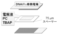
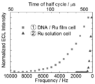
2+修飾電極間(電極間距離75μm)に過塩素酸テトラ-n-ブチルアンモニウムの炭酸プロピレン溶液(100mmol/L)を挟み込み、ECL素子を作製した。このECL素子の電気化学特性及び矩形波交流電圧印加時の電気化学発光特性の評価を行った。なお作製した表示装置の概略を図4に、この電気化学発光特性を図5に示しておく。なおこの電気化学発光特性の測定は、表示装置の電極間に±4V矩形波交流電圧を印加し、高周波数から低周波数へ印加周波数を掃引させた際の発光強度-周波数特性を示す。また、比較例として、通常のITO電極の間に上記Ru(bpy)3Cl2水溶液を挟持させた表示装置を作製して用いた。
この結果、10000Hzより、波長620nm付近にピークを持つオレンジ色の電気化学発光が認められ、周波数の低下とともにこの発光強度は増大した。Ru錯体を電解液中に溶解させた同面積のITO/ITO素子の発光が600Hzで開始したのと比較し、非常に高い周波数でECLが得られることが明らかとなった。10000Hz交流電圧を印加した際の電流・発光の応答性を測定したところ、50μ秒以下での発光の応答が観測された。
以上、これら実施例により、本発明の有用性が確認できた。
本発明は、表示装置及びこれに用いられる発光材料として産業上の利用可能性がある。
Claims (6)
- デオキシリボ核酸と、
前記デオキシリボ核酸のリン酸基に静電的に結合する脂質化合物と、
発光性物質と、を含む発光材料。 - 前記脂質化合物は、炭素数が10以上の四級アンモニウム塩を含む請求項1記載の発光材料。
- 前記発光性物質の重量を1とした場合に、デオキシリボ核酸及び前記脂質化合物の重量が1以上10未満の範囲内にある請求項1記載の発光材料。
- 一対の基板と、
前記一対の基板の間に挟持される発光材料と、を備える表示装置であって、
前記発光材料は、デオキシリボ核酸と、前記デオキシリボ核酸のリン酸基に静電的に結合する脂質化合物と、発光性物質と、を含むことを特徴とする表示装置。 - 前記発光材料の脂質化合物は、炭素数が10以上の四級アンモニウム塩を含む請求項4記載の表示装置。
- 前記発光性物質の重量を1とした場合に、デオキシリボ核酸及び前記脂質化合物の重量が1以上10未満の範囲内にある請求項4記載の表示装置。
Priority Applications (1)
| Application Number | Priority Date | Filing Date | Title |
|---|---|---|---|
| JP2015556319A JP6218291B2 (ja) | 2014-09-02 | 2015-08-28 | 発光材料及びこれを用いた表示装置。 |
Applications Claiming Priority (2)
| Application Number | Priority Date | Filing Date | Title |
|---|---|---|---|
| JP2014178604 | 2014-09-02 | ||
| JP2014-178604 | 2014-09-02 |
Publications (1)
| Publication Number | Publication Date |
|---|---|
| WO2016035722A1 true WO2016035722A1 (ja) | 2016-03-10 |
Family
ID=55439785
Family Applications (1)
| Application Number | Title | Priority Date | Filing Date |
|---|---|---|---|
| PCT/JP2015/074547 Ceased WO2016035722A1 (ja) | 2014-09-02 | 2015-08-28 | 発光材料及びこれを用いた表示装置。 |
Country Status (2)
| Country | Link |
|---|---|
| JP (1) | JP6218291B2 (ja) |
| WO (1) | WO2016035722A1 (ja) |
Cited By (1)
| Publication number | Priority date | Publication date | Assignee | Title |
|---|---|---|---|---|
| JPWO2023277110A1 (ja) * | 2021-06-30 | 2023-01-05 |
Citations (2)
| Publication number | Priority date | Publication date | Assignee | Title |
|---|---|---|---|---|
| JP2012036228A (ja) * | 2010-08-03 | 2012-02-23 | Ogata Zairyo Kagaku Kenkyusho:Kk | 発光材料及び有機発光素子 |
| JP2012036227A (ja) * | 2010-08-03 | 2012-02-23 | Ogata Zairyo Kagaku Kenkyusho:Kk | 発光材料及びその製造方法並びに有機発光素子 |
-
2015
- 2015-08-28 WO PCT/JP2015/074547 patent/WO2016035722A1/ja not_active Ceased
- 2015-08-28 JP JP2015556319A patent/JP6218291B2/ja active Active
Patent Citations (2)
| Publication number | Priority date | Publication date | Assignee | Title |
|---|---|---|---|---|
| JP2012036228A (ja) * | 2010-08-03 | 2012-02-23 | Ogata Zairyo Kagaku Kenkyusho:Kk | 発光材料及び有機発光素子 |
| JP2012036227A (ja) * | 2010-08-03 | 2012-02-23 | Ogata Zairyo Kagaku Kenkyusho:Kk | 発光材料及びその製造方法並びに有機発光素子 |
Non-Patent Citations (8)
| Title |
|---|
| "DNA/Kidorui Sakutai Fukugotai no Sogo Sayo to Hikari Butsuri Tokusei", THE 91TH ANNUAL MEETING OF THE CHEMICAL SOCIETY OF JAPAN IN SPRING (2011) KOEN YOKOSHU III, 11 March 2011 (2011-03-11), pages 870 * |
| "DNA/Kinosei Bunshi Fukugotai no Hikari · Denki Tokusei to Yuki EL Soshi eno Tenkai", THE 60TH SYMPOSIUM ON MACROMOLECULES YOKOSHU, 13 September 2011 (2011-09-13), pages 4737 - 4738 * |
| "Electroluminescence as a probe for elucidating electrical conductivity in a deoxyribonucleic acid-cetyltrimethylammonium lipid complex layer", APPLIED PHYSICS LETTERS, vol. 85, no. 9, 30 August 2004 (2004-08-30), pages 1627 - 1629 * |
| "Europium Sakutai to DNA-CTMA Fukugomaku ni Okeru Sekishoku Hakko Zokyo", ANNUAL MEETING ON PHOTOCHEMISTRY 2012 KOEN YOSHISHU, 7 September 2012 (2012-09-07), pages 137 * |
| "Kaimen Kasseizai ni yori Sosuika shita DNA Soshikitai ni yoru Yuki EL Soshi no Kochiku to Soshi Tokusei", THE 90TH ANNUAL MEETING OF THE CHEMICAL SOCIETY OF JAPAN IN SPRING (2010) KOEN YOKOSHU, 12 March 2010 (2010-03-12), pages 830 * |
| "Optical Property of Rare Earth Chelate Doped DNA-Lipid Complex", SYMPOSIUM ON MACROMOLECULES, vol. 63, no. 9, September 2006 (2006-09-01), pages 641 - 644 * |
| "Photophysical properties of lanthanide(III) chelates-doped DNA-CTMA complex", PROC. OF SPIE, vol. 8103, 2011, pages 810306 - 1-810306-7 * |
| "Submilli Byo Oto o Kano ni suru Koryu Kudogata DNA/Ru(bpy)32+ Fukugotai Denki Kagaku Hakko Soshi", 2014 NEN THE ELECTROCHEMICAL SOCIETY OF JAPAN DAI 81 KAI TAIKAI KOEN YOSHISHU, 29 March 2014 (2014-03-29), pages 19 * |
Cited By (2)
| Publication number | Priority date | Publication date | Assignee | Title |
|---|---|---|---|---|
| JPWO2023277110A1 (ja) * | 2021-06-30 | 2023-01-05 | ||
| WO2023277110A1 (ja) * | 2021-06-30 | 2023-01-05 | 国立大学法人千葉大学 | 発光材料およびその用途 |
Also Published As
| Publication number | Publication date |
|---|---|
| JPWO2016035722A1 (ja) | 2017-04-27 |
| JP6218291B2 (ja) | 2017-10-25 |
Similar Documents
| Publication | Publication Date | Title |
|---|---|---|
| Chen et al. | Two-photon absorption-based upconverted circularly polarized luminescence generated in chiral perovskite nanocrystals | |
| Zu et al. | Electrogenerated chemiluminescence. 66. The role of direct coreactant oxidation in the ruthenium Tris (2, 2 ‘) bipyridyl/tripropylamine system and the effect of halide ions on the emission intensity | |
| Xia et al. | Printable fluorescent hydrogels based on self-assembling peptides | |
| JP5056564B2 (ja) | 液体発光素子、発光表示装置 | |
| Wang et al. | Chemically responsive luminescent switching in transparent flexible self-supporting [EuW 10 O 36] 9−-agarose nanocomposite thin films | |
| US20170371219A1 (en) | Display device | |
| Huang et al. | Near-infrared circularly polarized luminescent physical unclonable functions | |
| US20130113359A1 (en) | Field emission devices including nanotubes or other nanoscale articles | |
| Li et al. | Toward Large Dissymmetry Factor of Circularly Polarized Luminescence in Donor–Acceptor Hybrid Systems | |
| Xu et al. | Induced Red Circularly Polarized Luminescence Emission Promoted by Intermolecular Förster Resonance Energy Transfer through a Cholesteric Liquid Crystal Medium | |
| Hwang et al. | Improvement of brightness, color purity, and operational stability of electrochemiluminescence devices with diphenylanthracene derivatives | |
| Devadoss et al. | Highly sensitive detection of NADH using electrochemiluminescent nanocomposites | |
| Ma et al. | Constructing multi‐stimuli‐responsive luminescent materials through outer sphere electron transfer in ion pairs | |
| Gao et al. | First orange fluorescence composite film based on Sm-substituted tungstophosphate and its electrofluorochromic performance | |
| Okada et al. | Microfluidic electrogenerated chemiluminescence cells using aluminum-doped zinc oxide nanoparticles as an electron injection layer | |
| Qin et al. | Tetraphenylethylene@ Graphene oxide with switchable fluorescence triggered by mixed solvents for the application of repeated information encryption and decryption | |
| Zhu et al. | Dual‐emissive Iridium (III) Complexes as Phosphorescent Probes with Orthogonal Responses to Analyte Binding and Oxygen Quenching | |
| Xia et al. | Self-assembly of europium-containing polyoxometalates/tetra-n-alkyl ammonium with enhanced emission for Cu2+ detection | |
| JP6218291B2 (ja) | 発光材料及びこれを用いた表示装置。 | |
| Koinuma et al. | White electrogenerated chemiluminescence using an anthracene derivative host and fluorescent dopants for microfluidic self-emissive displays | |
| Reid et al. | Solution and solid-state electrochemiluminescence of a fac-tris (2-phenylpyridyl) iridium (III)-cored dendrimer | |
| CN106886113A (zh) | 电致变色显示元件 | |
| JP2011138743A (ja) | 発光表示素子および発光表示装置 | |
| Qi et al. | Guanine Analogue-Based Assemblies: Construction and Luminescence Functions | |
| WO2013171660A1 (en) | Light-emitting device comprising an electroluminescent metal-organic framework |
Legal Events
| Date | Code | Title | Description |
|---|---|---|---|
| ENP | Entry into the national phase |
Ref document number: 2015556319 Country of ref document: JP Kind code of ref document: A |
|
| 121 | Ep: the epo has been informed by wipo that ep was designated in this application |
Ref document number: 15838865 Country of ref document: EP Kind code of ref document: A1 |
|
| NENP | Non-entry into the national phase |
Ref country code: DE |
|
| 122 | Ep: pct application non-entry in european phase |
Ref document number: 15838865 Country of ref document: EP Kind code of ref document: A1 |