WO2016018747A1 - LOW TEMPERATURE MOLECULAR LAYER DEPOSITION OF SiCON - Google Patents
LOW TEMPERATURE MOLECULAR LAYER DEPOSITION OF SiCON Download PDFInfo
- Publication number
- WO2016018747A1 WO2016018747A1 PCT/US2015/041977 US2015041977W WO2016018747A1 WO 2016018747 A1 WO2016018747 A1 WO 2016018747A1 US 2015041977 W US2015041977 W US 2015041977W WO 2016018747 A1 WO2016018747 A1 WO 2016018747A1
- Authority
- WO
- WIPO (PCT)
- Prior art keywords
- precursor
- film
- range
- amine
- precursor comprises
- Prior art date
- Legal status (The legal status is an assumption and is not a legal conclusion. Google has not performed a legal analysis and makes no representation as to the accuracy of the status listed.)
- Ceased
Links
Classifications
-
- H—ELECTRICITY
- H10—SEMICONDUCTOR DEVICES; ELECTRIC SOLID-STATE DEVICES NOT OTHERWISE PROVIDED FOR
- H10P—GENERIC PROCESSES OR APPARATUS FOR THE MANUFACTURE OR TREATMENT OF DEVICES COVERED BY CLASS H10
- H10P14/00—Formation of materials, e.g. in the shape of layers or pillars
- H10P14/60—Formation of materials, e.g. in the shape of layers or pillars of insulating materials
- H10P14/63—Formation of materials, e.g. in the shape of layers or pillars of insulating materials characterised by the formation processes
- H10P14/6326—Deposition processes
- H10P14/6328—Deposition from the gas or vapour phase
- H10P14/6334—Deposition from the gas or vapour phase using decomposition or reaction of gaseous or vapour phase compounds, i.e. chemical vapour deposition
- H10P14/6339—Deposition from the gas or vapour phase using decomposition or reaction of gaseous or vapour phase compounds, i.e. chemical vapour deposition deposition by cyclic CVD, e.g. ALD, ALE or pulsed CVD
-
- C—CHEMISTRY; METALLURGY
- C23—COATING METALLIC MATERIAL; COATING MATERIAL WITH METALLIC MATERIAL; CHEMICAL SURFACE TREATMENT; DIFFUSION TREATMENT OF METALLIC MATERIAL; COATING BY VACUUM EVAPORATION, BY SPUTTERING, BY ION IMPLANTATION OR BY CHEMICAL VAPOUR DEPOSITION, IN GENERAL; INHIBITING CORROSION OF METALLIC MATERIAL OR INCRUSTATION IN GENERAL
- C23C—COATING METALLIC MATERIAL; COATING MATERIAL WITH METALLIC MATERIAL; SURFACE TREATMENT OF METALLIC MATERIAL BY DIFFUSION INTO THE SURFACE, BY CHEMICAL CONVERSION OR SUBSTITUTION; COATING BY VACUUM EVAPORATION, BY SPUTTERING, BY ION IMPLANTATION OR BY CHEMICAL VAPOUR DEPOSITION, IN GENERAL
- C23C16/00—Chemical coating by decomposition of gaseous compounds, without leaving reaction products of surface material in the coating, i.e. chemical vapour deposition [CVD] processes
- C23C16/22—Chemical coating by decomposition of gaseous compounds, without leaving reaction products of surface material in the coating, i.e. chemical vapour deposition [CVD] processes characterised by the deposition of inorganic material, other than metallic material
- C23C16/30—Deposition of compounds, mixtures or solid solutions, e.g. borides, carbides, nitrides
-
- C—CHEMISTRY; METALLURGY
- C23—COATING METALLIC MATERIAL; COATING MATERIAL WITH METALLIC MATERIAL; CHEMICAL SURFACE TREATMENT; DIFFUSION TREATMENT OF METALLIC MATERIAL; COATING BY VACUUM EVAPORATION, BY SPUTTERING, BY ION IMPLANTATION OR BY CHEMICAL VAPOUR DEPOSITION, IN GENERAL; INHIBITING CORROSION OF METALLIC MATERIAL OR INCRUSTATION IN GENERAL
- C23C—COATING METALLIC MATERIAL; COATING MATERIAL WITH METALLIC MATERIAL; SURFACE TREATMENT OF METALLIC MATERIAL BY DIFFUSION INTO THE SURFACE, BY CHEMICAL CONVERSION OR SUBSTITUTION; COATING BY VACUUM EVAPORATION, BY SPUTTERING, BY ION IMPLANTATION OR BY CHEMICAL VAPOUR DEPOSITION, IN GENERAL
- C23C16/00—Chemical coating by decomposition of gaseous compounds, without leaving reaction products of surface material in the coating, i.e. chemical vapour deposition [CVD] processes
- C23C16/44—Chemical coating by decomposition of gaseous compounds, without leaving reaction products of surface material in the coating, i.e. chemical vapour deposition [CVD] processes characterised by the method of coating
- C23C16/455—Chemical coating by decomposition of gaseous compounds, without leaving reaction products of surface material in the coating, i.e. chemical vapour deposition [CVD] processes characterised by the method of coating characterised by the method used for introducing gases into reaction chamber or for modifying gas flows in reaction chamber
- C23C16/45523—Pulsed gas flow or change of composition over time
- C23C16/45525—Atomic layer deposition [ALD]
- C23C16/45527—Atomic layer deposition [ALD] characterized by the ALD cycle, e.g. different flows or temperatures during half-reactions, unusual pulsing sequence, use of precursor mixtures or auxiliary reactants or activations
- C23C16/45531—Atomic layer deposition [ALD] characterized by the ALD cycle, e.g. different flows or temperatures during half-reactions, unusual pulsing sequence, use of precursor mixtures or auxiliary reactants or activations specially adapted for making ternary or higher compositions
-
- C—CHEMISTRY; METALLURGY
- C23—COATING METALLIC MATERIAL; COATING MATERIAL WITH METALLIC MATERIAL; CHEMICAL SURFACE TREATMENT; DIFFUSION TREATMENT OF METALLIC MATERIAL; COATING BY VACUUM EVAPORATION, BY SPUTTERING, BY ION IMPLANTATION OR BY CHEMICAL VAPOUR DEPOSITION, IN GENERAL; INHIBITING CORROSION OF METALLIC MATERIAL OR INCRUSTATION IN GENERAL
- C23C—COATING METALLIC MATERIAL; COATING MATERIAL WITH METALLIC MATERIAL; SURFACE TREATMENT OF METALLIC MATERIAL BY DIFFUSION INTO THE SURFACE, BY CHEMICAL CONVERSION OR SUBSTITUTION; COATING BY VACUUM EVAPORATION, BY SPUTTERING, BY ION IMPLANTATION OR BY CHEMICAL VAPOUR DEPOSITION, IN GENERAL
- C23C16/00—Chemical coating by decomposition of gaseous compounds, without leaving reaction products of surface material in the coating, i.e. chemical vapour deposition [CVD] processes
- C23C16/56—After-treatment
-
- H—ELECTRICITY
- H10—SEMICONDUCTOR DEVICES; ELECTRIC SOLID-STATE DEVICES NOT OTHERWISE PROVIDED FOR
- H10P—GENERIC PROCESSES OR APPARATUS FOR THE MANUFACTURE OR TREATMENT OF DEVICES COVERED BY CLASS H10
- H10P14/00—Formation of materials, e.g. in the shape of layers or pillars
- H10P14/60—Formation of materials, e.g. in the shape of layers or pillars of insulating materials
- H10P14/69—Inorganic materials
- H10P14/692—Inorganic materials composed of oxides, glassy oxides or oxide-based glasses
- H10P14/6921—Inorganic materials composed of oxides, glassy oxides or oxide-based glasses containing silicon
- H10P14/6922—Inorganic materials composed of oxides, glassy oxides or oxide-based glasses containing silicon the material containing Si, O and at least one of H, N, C, F or other non-metal elements, e.g. SiOC, SiOC:H or SiONC
Definitions
- Embodiments of the disclosure generally relate to methods for molecular layer deposition. More specifically, embodiments of the disclosure are directed to methods for the molecular layer deposition of silicon carbon oxynitride (SiCON) films.
- SiCON silicon carbon oxynitride
- Deposition of thin films on a substrate surface is an important process in a variety of industries including semiconductor processing, diffusion barrier coatings and dielectrics for magnetic read/write heads.
- semiconductor processing in particular, miniaturization requires atomic level control of thin film deposition to produce conformal coatings on high aspect ratio structures.
- SiCON Silicon carbon oxynitride
- SiCON/SiCN Silicon carbide (oxy)nitride
- these drawbacks include a high temperature requirement (> 550 °C), few capabilities to engineer film compositions and bonding structures. These properties impact wet etch resistance and electrical stability during thermal cycling for front-end of line (FEOL) applications. Films deposited via plasma enhanced chemical vapor deposition (PE-CVD) at lower temperature have poor step coverage due to directionality of the radicals' fluxes.
- PE-CVD plasma enhanced chemical vapor deposition
- One or more embodiments of the disclosure are directed to methods of depositing a film. At least a portion of a substrate surface is exposed to a first precursor comprising a multi-functional amine to form an amine-containing film on the substrate surface. The amine- containing film is exposed to a second precursor comprising at least one silicon atom and at least one reactive moiety to form an SiCON film on at least a portion of the substrate surface.
- Additional embodiments of the disclosure are directed to methods of depositing a film. At least a portion of a substrate surface is exposed to a first precursor comprising a multi-functional amine to form an amine-containing film on the substrate surface.
- the first precursor comprises a compound having the formula selected from the group consisting of
- Unreacted first precursor is removed from the substrate surface.
- the amine-containing film is exposed to a second precursor comprising at least one silicon atom and at least one reactive moiety to form an SiCON film on at least a portion of the substrate surface.
- the reactive moiety is selected from the group consisting of isocyanato, aldehyde, ketone, acyl chloride, anhydrides and combinations thereof.
- Unreacted second precursor is removed from the substrate surface.
- the first precursor comprises a compound having the formula selected from the group consisting of
- Unreacted first precursor is removed from the substrate surface.
- the amine-containing film is exposed to a second precursor comprising at least one silicon atom and at least one reactive moiety to form an SiCON film on at least a portion of the substrate surface at a temperature in the range of about 50 °C to about 200 °C.
- the reactive moiety is selected from the group consisting of isocyanato, aldehyde, ketone, acyl chloride, anhydrides and combinations thereof.
- Unreacted second precursor is removed from the substrate surface.
- the exposure of at least a portion of the substrate surface to the first precursor, removing reacted first precursor, exposure to the second precursor and removing unreacted second precursor is sequentially repeated to form an SiCON film of a chosen thickness.
- the SiCON film is annealed in a gas selected from the group consisting of silane, dichlorosilane, trichlorosilane, ammonia, oxygen and combinations thereof.
- FIG. 1 illustrates an exemplary MLD process in accordance with one or more embodiment of the disclosure as described in the Example
- FIG. 2 shows an FTIR spectrum of the film deposited using the process of the Example as exemplified in FIG. 1.
- a "substrate surface” as used herein, refers to any substrate or material surface formed on a substrate upon which film processing is performed during a fabrication process.
- a substrate surface on which processing can be performed include materials such as silicon, silicon oxide, strained silicon, silicon on insulator (SOI), carbon doped silicon oxides, silicon nitride, doped silicon, germanium, gallium arsenide, glass, sapphire, and any other materials such as metals, metal nitrides, metal alloys, and other conductive materials, depending on the application.
- Substrates include, without limitation, semiconductor wafers.
- Substrates may be exposed to a pretreatment process to polish, etch, reduce, oxidize, hydroxylate, anneal and/or bake the substrate surface.
- a pretreatment process to polish, etch, reduce, oxidize, hydroxylate, anneal and/or bake the substrate surface.
- any of the film processing steps disclosed may also be performed on an underlayer formed on the substrate as disclosed in more detail below, and the term "substrate surface" is intended to include such underlayer as the context indicates.
- MLD molecular layer deposition
- Reactive moieties such as isocyanato groups (see equation 1), aldehydes or ketones (see equation 2), acyl chlorides (see equation 3) and anhydrides (see equation 4) can participate in MLD reactions with various amines such as ethylenediamine.
- Equations 1-4 show common organic reactions that occur between amines and aldehydes, ketones, acyl chlorides and anhydrides.
- the amine is at least bifunctional so that one amine can react with the substrate surface while the other amine may remain unreacted to participate in a subsequent ALD half-reaction.
- SiCON silicon, carbon, oxygen and nitrogen
- SiCON is used to describe a film having silicon, carbon, oxygen and nitrogen
- SiCON is merely representative of the majority makeup of the film.
- an SiCON film may also contain some other impurities or trace elements.
- an SiCON film may contain up to about 5% on an atomic basis of other elements, or up to about 4%, or up to about 3%, or up to about 2%, or up to about 1%, or up to about 0.5%, or up to about 0.2%.
- the amine is modified to contain more than two NH 2 groups. Without being bound by any particular theory of operation, it is believed that the amines can cross link the film and increase the mechanical strength.
- One or more embodiments of the disclosure involve the low temperature MLD of SiCON by the following method: First, a multifunctional amine is transported to a reaction chamber which will react with a substrate to form a layer of NH 2 groups on the surface. Next a purge is performed to get rid of any unreacted amine. Next a Si precursor is transported to the reactor chamber so that the precursor reacts with the NH 2 groups on the surface to form new carbon to nitrogen bonds. The chamber is purged to get rid of any unreacted Si precursor. Multiple cycles of this process should result in the low temperature deposition of SiCON. The deposition temperature can be 50 °C - 200 °C, and the pressures would be 0 - 300 Torr.
- the quality of the film can vary depending on a number of factors.
- the film formed might be of poor quality because of the low temperature and the relatively low density of the deposited film.
- annealing under gases such as (H 2 SiCl 2 , S1CI 3 , silane, NH 3 , 0 2 , etc.) may help densify the film and also tune the film's properties.
- one or more embodiment of the disclosure is directed to methods of depositing a film. At least a portion of a substrate surface is exposed to a first precursor comprising a multi-functional amine to form an amine-containing film on the substrate surface.
- the multi-functional amine comprises two amine groups, three amine groups, four amine groups, five amine groups or more.
- the first precursor comprises a compound having the formula
- n is up to about 16, or up to about 15, or up to about 14, or up to about 13, or up to about 12, or up to about 11, or up to about 10, or up to about 9, or up to about 8, or up to about 7, or up to about 6 or in the range of about 1 to about 8, or in the range of about 1 to about 6.
- the first precursor comprises a compound having the formula where n is up to about 16, or up to about 15, or up to about 14, or up to about 13, or up to about 12, or up to about 11, or up to about 10, or up to about 9, or up to about 8, or up to about 7, or up to about 6 or in the range of about 1 to about 8, or in the range of about 1 to about 6.
- the first precursor comprises a compound having the formula
- n is up to about 16, or up to about 15, or up to about 14, or up to about 13, or up to about 12, or up to about 11, or up to about 10, or up to about 9, or up to about 8, or up to about 7, or up to about 6 or in the range of about 1 to about 8, or in the range of about 1 to about 6.
- the first precursor comprises a compound having the formula selected from the group consisting of or combinations thereof, where n is up to about 16, or up to about 15, or up to about 14, or up to about 13, or up to about 12, or up to about 11, or up to about 10, or up to about 9, or up to about 8, or up to about 7, or up to about 6 or in the range of about 1 to about 8, or in the range of about 1 to about 6.
- the processing chamber, or substrate surface may be purged of excess or unreacted first precursor. This prevents any gas phase reactions between the first precursor and a subsequent second precursor.
- CVD chemical vapor deposition
- the first and second precursors may be exposed simultaneously.
- the entire processing chamber might be purged of the first precursor before exposure to the second precursor.
- the first precursor and the second precursor are flowed into separate portions of the processing chamber and are separated by a gas curtain to prevent gas phase reactions.
- the substrate is moved between the different regions of the processing chamber through the gas curtain so that different portions of the substrate are exposed to the first and second precursors at the same time.
- the amine- containing film can be exposed to a second precursor.
- the second precursor comprises a silicon atom and at least one reactive moiety to form an SiCON film on at least a portion of the substrate surface.
- the reactive moiety of the second precursor comprises an isocyanato group.
- the reactive moiety of the second precursor comprises an aldehyde.
- the reactive moiety of the second precursor comprises a ketone.
- the reactive moiety of the second precursor comprises an acyl chloride.
- the reactive moiety of the second precursor comprises an anhydride.
- the reactive moiety of the second precursor is selected from the group consisting of isocyanato, aldehyde, ketone, acyl chloride, anhydride and combinations thereof.
- the second precursor comprises a compound having the formula
- n is up to about 16, or up to about 15, or up to about 14, or up to about 13, or up to about 12, or up to about 11, or up to about 10, or up to about 9, or up to about 8, or up to about 7, or up to about 6 or in the range of about 1 to about 8, or in the range of about 1 to about 6, y is in the range of about 1 to about 3 and R is selected from the group consisting of hydrogen, alkyl groups, amino groups and combinations thereof.
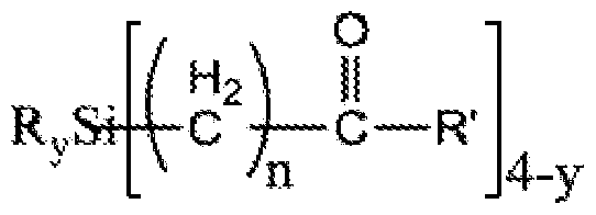
- the second precursor comprises a compound having the formula
- n is up to about 16, or up to about 15, or up to about 14, or up to about 13, or up to about 12, or up to about 11, or up to about 10, or up to about 9, or up to about 8, or up to about 7, or up to about 6 or in the range of about 1 to about 8, or in the range of about 1 to about 6, y is in the range of about 1 to about 3, R is selected from the group consisting of hydrogen, alkyl groups, amino groups and combinations thereof and R' is selected from the group consisting of hydrogen, alkyl groups or halides. [0030] In some embodiments, the second precursor comprises a compound having the formula
- each y is independently in the range of about 1 to about 2 and R is selected from the group consisting of hydrogen, alkyl groups, amino groups and combinations thereof.
- the second precursor comprises a compound having the formula selected from one or more of
- n is up to about 16, or up to about 15, or up to about 14, or up to about 13, or up to about 12, or up to about 11, or up to about 10, or up to about 9, or up to about 8, or up to about 7, or up to about 6 or in the range of about 1 to about 8, or in the range of about 1 to about 6, y is in the range of about 1 to about 3 and R is selected from the group consisting of hydrogen, alkyl groups, amino groups and combinations thereof,
- each y is independently in the range of about 1 to about 2 and R is selected from the group consisting of hydrogen, alkyl groups, amino groups and combinations thereof.
- the processing chamber, or substrate surface may be purged of excess or unreacted second precursor. This prevents any gas phase reactions between the second precursor and a subsequent first precursor.
- Some embodiments of the method further comprise annealing the SiCON film.
- the film can be annealed under an inert atmosphere or a reactive atmosphere. Without being bound by any particular theory of operation, it is believed that annealing the film can result in densification and strengthening of the film.
- the film is annealed in an environment comprising a silicon-containing gas.
- the film is annealed under a gas selected from the group consisting of silane, dichlorosilane, trichlorosilane, ammonia, oxygen and combinations thereof.
- the temperature of the deposition process can be less than about 400 °C, 350 °C, 300 °C, 250 °C or 200 °C.
- the deposition temperature of the substrate surface during either the first precursor exposure, the second precursor exposure or both the first and second precursor exposures can be less than about 400 °C, 350 °C, 300 °C, 250 °C or 200 °C.
- the substrate surface is maintained at a temperature in the range of about 25°C to about 400 °C, or in the range of about 50 °C to about 300 °C or in the range of about 50 °C to about 200 °C during exposure to the first precursor and the second precursor.
- Example [0036] A SiCON film was deposited by an MLD process by sequential exposure to tetraisocyanato silicon (Si(NCO) 4 ); TICS) and ethylenediamine (EDA).
- FIG. 1 shows an illustration of the MLD of SiCON involving TICS and ethylenediamine.
- a silicon substrate with a native oxide was exposed to 20 seconds of ammonia plasma treatment (100W at 0.78 Torr). The substrate temperature was maintained at 125 °C throughout deposition.
- the TICS bubbler was maintained at a temperature of about 70 °C and the EDA bubbler was maintained at a temperature of about 23 °C. Nitrogen gas was flowed through the TICS bubbler at about 250 seems and through the EDA bubbler at about 250 seems.
- the chamber pressure was maintained at about 30-35 Torr during deposition with about 35 seconds of purge between precursors (5 seconds purge and 30 seconds pump). Two hundred cycles of first and second precursor with intervening purges was performed. A film of about 99A (measured by ellipsometry) of SiCON was deposited with a growth rate of about 0.5A/cycle.
- FIG. 2 shows the FTIR spectrum of the deposited film.
- XPS X-ray photoelectron spectroscopy
Landscapes
- Chemical & Material Sciences (AREA)
- General Chemical & Material Sciences (AREA)
- Chemical Kinetics & Catalysis (AREA)
- Engineering & Computer Science (AREA)
- Materials Engineering (AREA)
- Mechanical Engineering (AREA)
- Metallurgy (AREA)
- Organic Chemistry (AREA)
- Inorganic Chemistry (AREA)
- Chemical Vapour Deposition (AREA)
Abstract
Methods for the deposition of a SiCON film by molecular layer deposition using a multi-functional amine and a silicon containing precursor having a reactive moiety.
Description
LOW TEMPERATURE MOLECULAR LAYER DEPOSITION OF SiCON
TECHNICAL FIELD
[0001] Embodiments of the disclosure generally relate to methods for molecular layer deposition. More specifically, embodiments of the disclosure are directed to methods for the molecular layer deposition of silicon carbon oxynitride (SiCON) films.
BACKGROUND
[0002] Deposition of thin films on a substrate surface is an important process in a variety of industries including semiconductor processing, diffusion barrier coatings and dielectrics for magnetic read/write heads. In the semiconductor industry, in particular, miniaturization requires atomic level control of thin film deposition to produce conformal coatings on high aspect ratio structures.
[0003] Silicon carbon oxynitride (SiCON) is being considered for spacer and etch-stop layer applications due to a low dielectric constant (k). Excellent conformality coverage of dielectric films on high aspect ratio structures is needed as device nodes shrink down below 45 nm. Silicon carbide (oxy)nitride (SiCON/SiCN) films can exhibit some of these favorable qualities, but deposition of SiCON/SiCN films from furnace processes has several drawbacks. For example, these drawbacks include a high temperature requirement (> 550 °C), few capabilities to engineer film compositions and bonding structures. These properties impact wet etch resistance and electrical stability during thermal cycling for front-end of line (FEOL) applications. Films deposited via plasma enhanced chemical vapor deposition (PE-CVD) at lower temperature have poor step coverage due to directionality of the radicals' fluxes.
[0004] Accordingly, there is a need for improved methods for depositing various silicon containing films such as SiCN. SUMMARY
[0005] One or more embodiments of the disclosure are directed to methods of depositing a film. At least a portion of a substrate surface is exposed to a first precursor comprising a multi-functional amine to form an amine-containing film on the substrate surface. The amine-
containing film is exposed to a second precursor comprising at least one silicon atom and at least one reactive moiety to form an SiCON film on at least a portion of the substrate surface.
[0006] Additional embodiments of the disclosure are directed to methods of depositing a film. At least a portion of a substrate surface is exposed to a first precursor comprising a multi-functional amine to form an amine-containing film on the substrate surface. The first precursor comprises a compound having the formula selected from the group consisting of

[0007] Further embodiments of the disclosure are directed to methods of depositing a film. At least a portion of a substrate surface is exposed to a first precursor comprising a multifunctional amine to form an amine-containing film on the substrate surface at a temperature in the range of about 50 °C to about 200 °C. The first precursor comprises a compound having the formula selected from the group consisting of

[0008] Further features of embodiment of the present disclosure, their nature and various advantages will become more apparent upon consideration of the following detailed description, taken in conjunction with the accompanying drawings, which are also illustrative of the best mode contemplated by the applicants, and in which like reference characters refer to like parts throughout, where:
[0009] FIG. 1 illustrates an exemplary MLD process in accordance with one or more embodiment of the disclosure as described in the Example; and
[0010] FIG. 2 shows an FTIR spectrum of the film deposited using the process of the Example as exemplified in FIG. 1. DETAILED DESCRIPTION
[0011] Before describing several exemplary embodiments of the disclosure, it is to be understood that the disclosure is not limited to the details of construction or process steps set forth in the following description. The disclosure is capable of other embodiments and of being practiced or being carried out in various ways.
[0012] A "substrate surface" as used herein, refers to any substrate or material surface formed on a substrate upon which film processing is performed during a fabrication process. For example, a substrate surface on which processing can be performed include materials such as silicon, silicon oxide, strained silicon, silicon on insulator (SOI), carbon doped silicon oxides, silicon nitride, doped silicon, germanium, gallium arsenide, glass, sapphire, and any other materials such as metals, metal nitrides, metal alloys, and other conductive materials, depending on the application. Substrates include, without limitation, semiconductor wafers. Substrates may be exposed to a pretreatment process to polish, etch, reduce, oxidize, hydroxylate, anneal and/or bake the substrate surface. In addition to film processing directly on the surface of the substrate itself, in the embodiments of the present disclosure any of the
film processing steps disclosed may also be performed on an underlayer formed on the substrate as disclosed in more detail below, and the term "substrate surface" is intended to include such underlayer as the context indicates.
[0013] One or more embodiments of the disclosure use a variant of atomic layer deposition (ALD) called molecular layer deposition (MLD). MLD processes can be used to deposit polymers such as polyimide, polyamide, or polyurea. For example, MLD of polyurea may be performed by alternating exposures of 1,4-diisocyanatobutane with various amines, such as ethylenediamine or tris(2-aminoethyl)amine. The inventors have surprisingly found that silicon precursors comprising reactive moieties can also be deposited by MLD. Reactive moieties such as isocyanato groups (see equation 1), aldehydes or ketones (see equation 2), acyl chlorides (see equation 3) and anhydrides (see equation 4) can participate in MLD reactions with various amines such as ethylenediamine.
[0014] Equations 1-4 show common organic reactions that occur between amines and aldehydes, ketones, acyl chlorides and anhydrides.
Equation 1

O N'
+ H20 Equation 2
RNH2 + FT R" R"
O O
^
NH2 + R^ CI on 3
R J + HCI Equati
¾NH2R
+ H90 Equation 4
 [0015] In some embodiments, the amine is at least bifunctional so that one amine can react with the substrate surface while the other amine may remain unreacted to participate in a subsequent ALD half-reaction.
[0016] The inventors have found that a network of silicon, carbon, oxygen and nitrogen can be deposited using two precursors. While the term SiCON is used to describe a film having silicon, carbon, oxygen and nitrogen, it will be understood by those skilled in the art that no stoichiometry is intended by such formula. For example, an SiCON film is not limited to films with equal numbers of silicon, carbon, oxygen and nitrogen atoms, the term SiCON is merely representative of the majority makeup of the film. Additionally, it will be understood that an SiCON film may also contain some other impurities or trace elements. For example, an SiCON film may contain up to about 5% on an atomic basis of other elements, or up to about 4%, or up to about 3%, or up to about 2%, or up to about 1%, or up to about 0.5%, or up to about 0.2%.
[0017] In some embodiments, the amine is modified to contain more than two NH2 groups. Without being bound by any particular theory of operation, it is believed that the amines can cross link the film and increase the mechanical strength.
[0018] One or more embodiments of the disclosure involve the low temperature MLD of SiCON by the following method: First, a multifunctional amine is transported to a reaction chamber which will react with a substrate to form a layer of NH2 groups on the surface. Next a purge is performed to get rid of any unreacted amine. Next a Si precursor is transported to the reactor chamber so that the precursor reacts with the NH2 groups on the surface to form new carbon to nitrogen bonds. The chamber is purged to get rid of any unreacted Si precursor. Multiple cycles of this process should result in the low temperature deposition of SiCON. The deposition temperature can be 50 °C - 200 °C, and the pressures would be 0 - 300 Torr. [0019] The quality of the film can vary depending on a number of factors. The film formed might be of poor quality because of the low temperature and the relatively low density of the deposited film. In some embodiments, annealing under gases such as (H2SiCl2, S1CI3, silane, NH3, 02, etc.) may help densify the film and also tune the film's properties.
[0020] Accordingly, one or more embodiment of the disclosure is directed to methods of depositing a film. At least a portion of a substrate surface is exposed to a first precursor comprising a multi-functional amine to form an amine-containing film on the substrate surface.
In some embodiments, the multi-functional amine comprises two amine groups, three amine groups, four amine groups, five amine groups or more.
[0021] In some embodiments, the first precursor comprises a compound having the formula

[0022] In some embodiments, the first precursor comprises a compound having the formula
 where n is up to about 16, or up to about 15, or up to about 14, or up to about 13, or up to about 12, or up to about 11, or up to about 10, or up to about 9, or up to about 8, or up to about 7, or up to about 6 or in the range of about 1 to about 8, or in the range of about 1 to about 6.
[0023] In some embodiments, the first precursor comprises a compound having the formula

[0024] In some embodiments, the first precursor comprises a compound having the formula selected from the group consisting of
 or combinations thereof, where n is up to about 16, or up to about 15, or up to about 14, or up to about 13, or up to about 12, or up to about 11, or up to about 10, or up to about 9, or up to about 8, or up to about 7, or up to about 6 or in the range of about 1 to about 8, or in the range of about 1 to about 6.
[0025] In some embodiments, after exposure to the first precursor, the processing chamber, or substrate surface may be purged of excess or unreacted first precursor. This prevents any gas phase reactions between the first precursor and a subsequent second precursor. When a chemical vapor deposition (CVD) reaction is intended, there is no need to purge between the exposure to the first and second precursor. For a CVD reaction, the first and second precursors may be exposed simultaneously.
[0026] In a traditional time-domain ALD process, the entire processing chamber might be purged of the first precursor before exposure to the second precursor. In a spatial ALD process, the first precursor and the second precursor are flowed into separate portions of the processing chamber and are separated by a gas curtain to prevent gas phase reactions. In the spatial process, the substrate is moved between the different regions of the processing chamber through the gas curtain so that different portions of the substrate are exposed to the first and second precursors at the same time.
[0027] In the ALD type process, after formation of the amine-containing film, the amine- containing film can be exposed to a second precursor. The second precursor comprises a silicon atom and at least one reactive moiety to form an SiCON film on at least a portion of the substrate surface. In some embodiments, the reactive moiety of the second precursor comprises an isocyanato group. In some embodiments, the reactive moiety of the second precursor comprises an aldehyde. In some embodiments, the reactive moiety of the second precursor comprises a ketone. In some embodiments, the reactive moiety of the second precursor comprises an acyl chloride. In some embodiments, the reactive moiety of the second precursor comprises an anhydride. In some embodiments, the reactive moiety of the second
precursor is selected from the group consisting of isocyanato, aldehyde, ketone, acyl chloride, anhydride and combinations thereof.
[0028] In one or more embodiments, the second precursor comprises a compound having the formula

where n is up to about 16, or up to about 15, or up to about 14, or up to about 13, or up to about 12, or up to about 11, or up to about 10, or up to about 9, or up to about 8, or up to about 7, or up to about 6 or in the range of about 1 to about 8, or in the range of about 1 to about 6, y is in the range of about 1 to about 3 and R is selected from the group consisting of hydrogen, alkyl groups, amino groups and combinations thereof.
[0029] In some embodiments, the second precursor comprises a compound having the formula

[0031] In one or more embodiments, the second precursor comprises a compound having the formula selected from one or more of

where n is up to about 16, or up to about 15, or up to about 14, or up to about 13, or up to about 12, or up to about 11, or up to about 10, or up to about 9, or up to about 8, or up to about 7, or up to about 6 or in the range of about 1 to about 8, or in the range of about 1 to about 6, y is in the range of about 1 to about 3 and R is selected from the group consisting of hydrogen, alkyl groups, amino groups and combinations thereof,

[0032] In some embodiments, after exposure to the second precursor, the processing chamber, or substrate surface may be purged of excess or unreacted second precursor. This prevents any gas phase reactions between the second precursor and a subsequent first precursor.
[0033] Some embodiments of the method further comprise annealing the SiCON film. The film can be annealed under an inert atmosphere or a reactive atmosphere. Without being bound by any particular theory of operation, it is believed that annealing the film can result in densification and strengthening of the film. In one or more embodiments, the film is annealed in an environment comprising a silicon-containing gas. In one or more embodiments, the film is annealed under a gas selected from the group consisting of silane, dichlorosilane, trichlorosilane, ammonia, oxygen and combinations thereof.
[0034] The temperature of the deposition process can be less than about 400 °C, 350 °C, 300 °C, 250 °C or 200 °C. In some embodiments, the deposition temperature of the substrate surface during either the first precursor exposure, the second precursor exposure or both the first and second precursor exposures can be less than about 400 °C, 350 °C, 300 °C, 250 °C or 200 °C. In one or more embodiments, the substrate surface is maintained at a temperature in the range of about 25°C to about 400 °C, or in the range of about 50 °C to about 300 °C or in the range of about 50 °C to about 200 °C during exposure to the first precursor and the second precursor.
[0035] Example [0036] A SiCON film was deposited by an MLD process by sequential exposure to tetraisocyanato silicon (Si(NCO)4); TICS) and ethylenediamine (EDA). FIG. 1 shows an illustration of the MLD of SiCON involving TICS and ethylenediamine. A silicon substrate with a native oxide was exposed to 20 seconds of ammonia plasma treatment (100W at 0.78 Torr). The substrate temperature was maintained at 125 °C throughout deposition. The TICS bubbler was maintained at a temperature of about 70 °C and the EDA bubbler was maintained at a temperature of about 23 °C. Nitrogen gas was flowed through the TICS bubbler at about 250 seems and through the EDA bubbler at about 250 seems. The chamber pressure was maintained at about 30-35 Torr during deposition with about 35 seconds of purge between precursors (5 seconds purge and 30 seconds pump). Two hundred cycles of first and second precursor with intervening purges was performed. A film of about 99A (measured by ellipsometry) of SiCON was deposited with a growth rate of about 0.5A/cycle.
[0037] FIG. 2 shows the FTIR spectrum of the deposited film. The FTIR spectrum is labelled with resonances believed to belong to NH, CH2, C=), H-NCO, and Si-0 or Si-N bonding. [0038] X-ray photoelectron spectroscopy (XPS) results of the deposited film are shown in Table 1.
Table 1. XPS Results of the Film De osited
 0.0 28.9 21.7 33.2 16.2
15.0 11.8 12.6 42.1 33.5
30.0 5.9 8.4 42.6 43.2
45.0 3.0 5.4 39.4 52.2
[0039] Reference throughout this specification to "one embodiment," "certain embodiments," "various embodiments," "one or more embodiments," "in some embodiments," or "an embodiment" means that a particular feature, structure, material, or characteristic described in connection with the embodiment may be included in at least one embodiment of the disclosure. Furthermore, the appearances of the phrases such as "in one or more embodiments," "in certain embodiments," "in some embodiments," "in one embodiment" or "in an embodiment" in various places throughout this specification are not necessarily referring to the same embodiment of the disclosure. In addition, the particular features, structures, materials, or characteristics described may be combined in any suitable manner in one or more embodiments.
[0040] Although the disclosure herein has been described with reference to particular embodiments, it is to be understood that these embodiments are merely illustrative of the principles and applications of the present disclosure. It will be apparent to those skilled in the art that various modifications and variations can be made to the material, method, and apparatus of the present disclosure without departing from the spirit and scope of the disclosure. Thus, it is intended that the present disclosure include modifications and variations that are within the scope of the appended claims and their equivalents.
Claims
claimed is:
A method of depositing a film, the method comprising:
exposing at least a portion of a substrate surface to a first precursor comprising a multi-functional amine to form an amine-containing film on the substrate surface; and exposing the amine-containing film to a second precursor comprising at least one silicon atom and at least one reactive moiety to form an SiCON film on at least a portion of the substrate surface.
The method of claim 1, wherein the multi-functional amine comprises two amine groups.
The method of claim 1, wherein the multi-functional amine comprises three amine groups.
The method of claim 1, wherein the first precursor comprises a compound having the formula

where n is in the range of about 1 and about 6.
The method of claim 1, wherein the first precursor comprises a compound having the formula
 where n is in the range of about 1 and about 6.
The method of claim 1, wherein the first precursor comprises a compound having the formula

The method of claim 1, wherein the reactive moiety of the second precursor comprises an isocyanato group.
8. The method of claim 1, wherein the reactive moiety of the second precursor comprises an aldehyde. 9. The method of claim 1, wherein the reactive moiety of the second precursor comprises a ketone.
10. The method of claim 1, wherein the reactive moiety of the second precursor comprises an acyl chloride.
11. The method of claim 1, wherein the reactive moiety of the second precursor comprises an anhydride.
12. The method of claim 1, wherein the second precursor comprises a compound having the formula

where n is in the range of about 0 to about 6, y is in the range of about 1 to about 3 and R is selected from the group consisting of hydrogen, alkyl groups, amino groups and combinations thereof.
13. The method of claim 1, wherein the second precursor comprises a compound having the formula

where n is in the range of about 0 to about 6, y is in the range of about 1 to about 3, R is selected from the group consisting of hydrogen, alkyl groups, amino groups and combinations thereof and R' is selected from the group consisting of hydrogen, alkyl groups or halides.
The method of claim 1, wherein the second precursor comprises a compound having the formula

where each y is independently in the range of about 1 to about 2 and R is selected from the group consisting of hydrogen, alkyl groups, amino groups and combinations thereof.
15. The method of claim 1, further comprising annealing the SiCON film under a gas selected from the group consisting of silane, dichlorosilane, trichlorosilane, ammonia, oxygen and combinations thereof.
Priority Applications (1)
| Application Number | Priority Date | Filing Date | Title |
|---|---|---|---|
| KR1020177005418A KR102380197B1 (en) | 2014-07-26 | 2015-07-24 | LOW TEMPERATURE MOLECULAR LAYER DEPOSITION OF SiCON |
Applications Claiming Priority (4)
| Application Number | Priority Date | Filing Date | Title |
|---|---|---|---|
| US201462029479P | 2014-07-26 | 2014-07-26 | |
| US62/029,479 | 2014-07-26 | ||
| US14/801,215 US9812318B2 (en) | 2014-07-26 | 2015-07-16 | Low temperature molecular layer deposition of SiCON |
| US14/801,215 | 2015-07-16 |
Publications (1)
| Publication Number | Publication Date |
|---|---|
| WO2016018747A1 true WO2016018747A1 (en) | 2016-02-04 |
Family
ID=55166247
Family Applications (1)
| Application Number | Title | Priority Date | Filing Date |
|---|---|---|---|
| PCT/US2015/041977 Ceased WO2016018747A1 (en) | 2014-07-26 | 2015-07-24 | LOW TEMPERATURE MOLECULAR LAYER DEPOSITION OF SiCON |
Country Status (4)
| Country | Link |
|---|---|
| US (2) | US9812318B2 (en) |
| KR (1) | KR102380197B1 (en) |
| TW (1) | TW201610204A (en) |
| WO (1) | WO2016018747A1 (en) |
Families Citing this family (19)
| Publication number | Priority date | Publication date | Assignee | Title |
|---|---|---|---|---|
| TW201610204A (en) * | 2014-07-26 | 2016-03-16 | 應用材料股份有限公司 | Low temperature molecular layer deposition of bismuth oxycarbonitride |
| US20180022691A1 (en) | 2016-07-21 | 2018-01-25 | Versum Materials Us, Llc | High Purity Ethylenediamine for Semiconductor Applications |
| US11735413B2 (en) | 2016-11-01 | 2023-08-22 | Versum Materials Us, Llc | Precursors and flowable CVD methods for making low-k films to fill surface features |
| US10176984B2 (en) | 2017-02-14 | 2019-01-08 | Lam Research Corporation | Selective deposition of silicon oxide |
| US10242866B2 (en) | 2017-03-08 | 2019-03-26 | Lam Research Corporation | Selective deposition of silicon nitride on silicon oxide using catalytic control |
| US10043656B1 (en) | 2017-03-10 | 2018-08-07 | Lam Research Corporation | Selective growth of silicon oxide or silicon nitride on silicon surfaces in the presence of silicon oxide |
| US9911595B1 (en) | 2017-03-17 | 2018-03-06 | Lam Research Corporation | Selective growth of silicon nitride |
| US10559461B2 (en) | 2017-04-19 | 2020-02-11 | Lam Research Corporation | Selective deposition with atomic layer etch reset |
| US10957543B2 (en) | 2017-09-29 | 2021-03-23 | Taiwan Semiconductor Manufacturing Co., Ltd. | Device and method of dielectric layer |
| US10460930B2 (en) | 2017-11-22 | 2019-10-29 | Lam Research Corporation | Selective growth of SiO2 on dielectric surfaces in the presence of copper |
| JP7089881B2 (en) * | 2018-01-10 | 2022-06-23 | 東京エレクトロン株式会社 | Film formation method |
| KR102899918B1 (en) | 2018-03-02 | 2025-12-12 | 램 리써치 코포레이션 | Selective deposition using hydrolysis |
| JP7431245B2 (en) | 2019-01-24 | 2024-02-14 | アプライド マテリアルズ インコーポレイテッド | How to deposit silicon nitride |
| EP4058188A4 (en) * | 2019-11-11 | 2024-01-31 | The Regents of the University of Colorado, a body corporate | PROCESS FOR SYNTHESIS OF SOLID CARBON CAPTURE MATERIALS |
| CN112824559A (en) * | 2019-11-20 | 2021-05-21 | 中国科学院微电子研究所 | Method for depositing silicon-carbon-nitrogen-oxygen molecular film at low temperature |
| US12142479B2 (en) * | 2020-01-17 | 2024-11-12 | Asm Ip Holding B.V. | Formation of SiOCN thin films |
| US11359281B2 (en) * | 2020-01-26 | 2022-06-14 | Applied Materials, Inc. | Selective deposition of SiCON by plasma ALD |
| US11859278B2 (en) * | 2020-03-08 | 2024-01-02 | Applied Materials, Inc. | Molecular layer deposition of amorphous carbon films |
| KR102935816B1 (en) * | 2024-07-03 | 2026-03-09 | 한양대학교 산학협력단 | SiONC thin film and its manufacturing method |
Citations (5)
| Publication number | Priority date | Publication date | Assignee | Title |
|---|---|---|---|---|
| US20060014399A1 (en) * | 2004-07-14 | 2006-01-19 | Tokyo Electron Limited | Low-temperature plasma-enhanced chemical vapor deposition of silicon-nitrogen-containing films |
| US20060228903A1 (en) * | 2005-03-30 | 2006-10-12 | Mcswiney Michael L | Precursors for the deposition of carbon-doped silicon nitride or silicon oxynitride films |
| US20100081293A1 (en) * | 2008-10-01 | 2010-04-01 | Applied Materials, Inc. | Methods for forming silicon nitride based film or silicon carbon based film |
| US8080282B2 (en) * | 2006-08-08 | 2011-12-20 | Asm Japan K.K. | Method for forming silicon carbide film containing oxygen |
| US20130164946A1 (en) * | 2011-12-27 | 2013-06-27 | Tokyo Electron Limited | Method of forming silicon oxycarbonitride film |
Family Cites Families (11)
| Publication number | Priority date | Publication date | Assignee | Title |
|---|---|---|---|---|
| US20040084774A1 (en) * | 2002-11-02 | 2004-05-06 | Bo Li | Gas layer formation materials |
| US7294449B1 (en) * | 2003-12-31 | 2007-11-13 | Kovio, Inc. | Radiation patternable functional materials, methods of their use, and structures formed therefrom |
| JP2008053507A (en) * | 2006-08-25 | 2008-03-06 | Matsushita Electric Ind Co Ltd | Dry etching method |
| JP5706755B2 (en) * | 2010-06-10 | 2015-04-22 | 東ソー株式会社 | Hydrosilane derivative, process for producing the same, process for producing silicon-containing thin film |
| US8647993B2 (en) * | 2011-04-11 | 2014-02-11 | Novellus Systems, Inc. | Methods for UV-assisted conformal film deposition |
| US9200167B2 (en) * | 2012-01-27 | 2015-12-01 | Air Products And Chemicals, Inc. | Alkoxyaminosilane compounds and applications thereof |
| JP6415808B2 (en) * | 2012-12-13 | 2018-10-31 | 株式会社Kokusai Electric | Semiconductor device manufacturing method, substrate processing apparatus, and program |
| WO2014134476A1 (en) * | 2013-03-01 | 2014-09-04 | Applied Materials, Inc. | LOW TEMPERATURE ATOMIC LAYER DEPOSITION OF FILMS COMPRISING SiCN OR SiCON |
| WO2015194901A1 (en) * | 2014-06-19 | 2015-12-23 | Lg Innotek Co., Ltd. | Inorganic filler, epoxy resin composition including the same and light emitting element including insulating layer using the composition |
| TW201610204A (en) * | 2014-07-26 | 2016-03-16 | 應用材料股份有限公司 | Low temperature molecular layer deposition of bismuth oxycarbonitride |
| US9786492B2 (en) * | 2015-11-12 | 2017-10-10 | Asm Ip Holding B.V. | Formation of SiOCN thin films |
-
2015
- 2015-07-06 TW TW104121881A patent/TW201610204A/en unknown
- 2015-07-16 US US14/801,215 patent/US9812318B2/en active Active
- 2015-07-24 KR KR1020177005418A patent/KR102380197B1/en active Active
- 2015-07-24 WO PCT/US2015/041977 patent/WO2016018747A1/en not_active Ceased
-
2017
- 2017-11-06 US US15/804,503 patent/US10354861B2/en active Active
Patent Citations (5)
| Publication number | Priority date | Publication date | Assignee | Title |
|---|---|---|---|---|
| US20060014399A1 (en) * | 2004-07-14 | 2006-01-19 | Tokyo Electron Limited | Low-temperature plasma-enhanced chemical vapor deposition of silicon-nitrogen-containing films |
| US20060228903A1 (en) * | 2005-03-30 | 2006-10-12 | Mcswiney Michael L | Precursors for the deposition of carbon-doped silicon nitride or silicon oxynitride films |
| US8080282B2 (en) * | 2006-08-08 | 2011-12-20 | Asm Japan K.K. | Method for forming silicon carbide film containing oxygen |
| US20100081293A1 (en) * | 2008-10-01 | 2010-04-01 | Applied Materials, Inc. | Methods for forming silicon nitride based film or silicon carbon based film |
| US20130164946A1 (en) * | 2011-12-27 | 2013-06-27 | Tokyo Electron Limited | Method of forming silicon oxycarbonitride film |
Also Published As
| Publication number | Publication date |
|---|---|
| US9812318B2 (en) | 2017-11-07 |
| TW201610204A (en) | 2016-03-16 |
| US10354861B2 (en) | 2019-07-16 |
| US20180061629A1 (en) | 2018-03-01 |
| KR20170038023A (en) | 2017-04-05 |
| US20160024647A1 (en) | 2016-01-28 |
| KR102380197B1 (en) | 2022-03-28 |
Similar Documents
| Publication | Publication Date | Title |
|---|---|---|
| KR102380197B1 (en) | LOW TEMPERATURE MOLECULAR LAYER DEPOSITION OF SiCON | |
| US11028478B2 (en) | Atomic layer deposition of films comprising silicon, carbon and nitrogen using halogenated silicon precursors | |
| US20230090196A1 (en) | Methods For Atomic Layer Deposition Of SiCO(N) Using Halogenated Silylamides | |
| KR102192161B1 (en) | Atomic layer deposition of GeO2 | |
| KR102415780B1 (en) | Carbon and/or nitrogen incorporation in silicon-based films using silicon precursors with organic co-reactants by pe-ald | |
| US9984868B2 (en) | PEALD of films comprising silicon nitride | |
| US11823893B2 (en) | Methods of depositing SiCON with C, O, and N compositional control | |
| US20090155606A1 (en) | Methods of depositing a silicon nitride film | |
| US9875889B2 (en) | Atomic layer deposition of films comprising Si(C)N using hydrazine, azide and/or silyl amine derivatives | |
| US20060208215A1 (en) | Method for hafnium nitride deposition | |
| JP7164789B2 (en) | Precursors and processes for depositing Si-containing films using ALD at temperatures above 550°C | |
| KR20150121217A (en) | LOW TEMPERATURE ATOMIC LAYER DEPOSITION OF FILMS COMPRISING SiCN OR SiCON | |
| JP6577695B2 (en) | Method for forming silicon nitride film | |
| US20110121430A1 (en) | Method for forming a silicon dioxide/metal oxide-nanolaminate with a desired wet etch rate | |
| TWI640651B (en) | Atomic layer deposition of films comprising silicon, carbon and nitrogen using halogenated silicon precursors | |
| KR102813568B1 (en) | Ultra-low temperature ALD for forming high quality Si-containing films | |
| KR102932239B1 (en) | Methods for atomic layer deposition of SiCO(N) using halogenated silylamides | |
| US12119223B2 (en) | Single precursor low-k film deposition and UV cure for advanced technology node | |
| CN122003519A (en) | Silicon-containing film having surface modified with halogenated silicon-containing compound | |
| CN112824559A (en) | Method for depositing silicon-carbon-nitrogen-oxygen molecular film at low temperature |
Legal Events
| Date | Code | Title | Description |
|---|---|---|---|
| 121 | Ep: the epo has been informed by wipo that ep was designated in this application |
Ref document number: 15826600 Country of ref document: EP Kind code of ref document: A1 |
|
| NENP | Non-entry into the national phase |
Ref country code: DE |
|
| ENP | Entry into the national phase |
Ref document number: 20177005418 Country of ref document: KR Kind code of ref document: A |
|
| 122 | Ep: pct application non-entry in european phase |
Ref document number: 15826600 Country of ref document: EP Kind code of ref document: A1 |