WO2015170331A2 - Inorganic nanomaterials - Google Patents
Inorganic nanomaterials Download PDFInfo
- Publication number
- WO2015170331A2 WO2015170331A2 PCT/IL2015/050479 IL2015050479W WO2015170331A2 WO 2015170331 A2 WO2015170331 A2 WO 2015170331A2 IL 2015050479 W IL2015050479 W IL 2015050479W WO 2015170331 A2 WO2015170331 A2 WO 2015170331A2
- Authority
- WO
- WIPO (PCT)
- Prior art keywords
- nanostructure
- nanomaterial
- las
- crs
- formula
- Prior art date
- Legal status (The legal status is an assumption and is not a legal conclusion. Google has not performed a legal analysis and makes no representation as to the accuracy of the status listed.)
- Ceased
Links
Classifications
-
- C—CHEMISTRY; METALLURGY
- C30—CRYSTAL GROWTH
- C30B—SINGLE-CRYSTAL GROWTH; UNIDIRECTIONAL SOLIDIFICATION OF EUTECTIC MATERIAL OR UNIDIRECTIONAL DEMIXING OF EUTECTOID MATERIAL; REFINING BY ZONE-MELTING OF MATERIAL; PRODUCTION OF A HOMOGENEOUS POLYCRYSTALLINE MATERIAL WITH DEFINED STRUCTURE; SINGLE CRYSTALS OR HOMOGENEOUS POLYCRYSTALLINE MATERIAL WITH DEFINED STRUCTURE; AFTER-TREATMENT OF SINGLE CRYSTALS OR A HOMOGENEOUS POLYCRYSTALLINE MATERIAL WITH DEFINED STRUCTURE; APPARATUS THEREFOR
- C30B29/00—Single crystals or homogeneous polycrystalline material with defined structure characterised by the material or by their shape
- C30B29/10—Inorganic compounds or compositions
- C30B29/46—Sulfur-, selenium- or tellurium-containing compounds
-
- B—PERFORMING OPERATIONS; TRANSPORTING
- B01—PHYSICAL OR CHEMICAL PROCESSES OR APPARATUS IN GENERAL
- B01J—CHEMICAL OR PHYSICAL PROCESSES, e.g. CATALYSIS OR COLLOID CHEMISTRY; THEIR RELEVANT APPARATUS
- B01J27/00—Catalysts comprising the elements or compounds of halogens, sulfur, selenium, tellurium, phosphorus or nitrogen; Catalysts comprising carbon compounds
- B01J27/02—Sulfur, selenium or tellurium; Compounds thereof
- B01J27/04—Sulfides
- B01J27/047—Sulfides with chromium, molybdenum, tungsten or polonium
-
- B—PERFORMING OPERATIONS; TRANSPORTING
- B01—PHYSICAL OR CHEMICAL PROCESSES OR APPARATUS IN GENERAL
- B01J—CHEMICAL OR PHYSICAL PROCESSES, e.g. CATALYSIS OR COLLOID CHEMISTRY; THEIR RELEVANT APPARATUS
- B01J35/00—Catalysts, in general, characterised by their form or physical properties
- B01J35/30—Catalysts, in general, characterised by their form or physical properties characterised by their physical properties
- B01J35/39—Photocatalytic properties
-
- C—CHEMISTRY; METALLURGY
- C01—INORGANIC CHEMISTRY
- C01B—NON-METALLIC ELEMENTS; COMPOUNDS THEREOF; METALLOIDS OR COMPOUNDS THEREOF NOT COVERED BY SUBCLASS C01C
- C01B19/00—Selenium; Tellurium; Compounds thereof
- C01B19/002—Compounds containing, besides selenium or tellurium, more than one other element, with -O- and -OH not being considered as anions
-
- C—CHEMISTRY; METALLURGY
- C01—INORGANIC CHEMISTRY
- C01F—COMPOUNDS OF THE METALS BERYLLIUM, MAGNESIUM, ALUMINIUM, CALCIUM, STRONTIUM, BARIUM, RADIUM, THORIUM, OR OF THE RARE-EARTH METALS
- C01F17/00—Compounds of rare earth metals
- C01F17/20—Compounds containing only rare earth metals as the metal element
- C01F17/288—Sulfides
-
- C—CHEMISTRY; METALLURGY
- C01—INORGANIC CHEMISTRY
- C01G—COMPOUNDS CONTAINING METALS NOT COVERED BY SUBCLASSES C01D OR C01F
- C01G1/00—Methods of preparing compounds of metals not covered by subclasses C01B, C01C, C01D, or C01F, in general
- C01G1/12—Sulfides
-
- C—CHEMISTRY; METALLURGY
- C01—INORGANIC CHEMISTRY
- C01G—COMPOUNDS CONTAINING METALS NOT COVERED BY SUBCLASSES C01D OR C01F
- C01G19/00—Compounds of tin
-
- C—CHEMISTRY; METALLURGY
- C01—INORGANIC CHEMISTRY
- C01G—COMPOUNDS CONTAINING METALS NOT COVERED BY SUBCLASSES C01D OR C01F
- C01G21/00—Compounds of lead
- C01G21/21—Sulfides
-
- C—CHEMISTRY; METALLURGY
- C01—INORGANIC CHEMISTRY
- C01G—COMPOUNDS CONTAINING METALS NOT COVERED BY SUBCLASSES C01D OR C01F
- C01G30/00—Compounds of antimony
- C01G30/008—Sulfides
-
- C—CHEMISTRY; METALLURGY
- C01—INORGANIC CHEMISTRY
- C01G—COMPOUNDS CONTAINING METALS NOT COVERED BY SUBCLASSES C01D OR C01F
- C01G31/00—Compounds of vanadium
-
- C—CHEMISTRY; METALLURGY
- C01—INORGANIC CHEMISTRY
- C01G—COMPOUNDS CONTAINING METALS NOT COVERED BY SUBCLASSES C01D OR C01F
- C01G33/00—Compounds of niobium
-
- C—CHEMISTRY; METALLURGY
- C01—INORGANIC CHEMISTRY
- C01G—COMPOUNDS CONTAINING METALS NOT COVERED BY SUBCLASSES C01D OR C01F
- C01G35/00—Compounds of tantalum
-
- C—CHEMISTRY; METALLURGY
- C01—INORGANIC CHEMISTRY
- C01G—COMPOUNDS CONTAINING METALS NOT COVERED BY SUBCLASSES C01D OR C01F
- C01G37/00—Compounds of chromium
-
- C—CHEMISTRY; METALLURGY
- C30—CRYSTAL GROWTH
- C30B—SINGLE-CRYSTAL GROWTH; UNIDIRECTIONAL SOLIDIFICATION OF EUTECTIC MATERIAL OR UNIDIRECTIONAL DEMIXING OF EUTECTOID MATERIAL; REFINING BY ZONE-MELTING OF MATERIAL; PRODUCTION OF A HOMOGENEOUS POLYCRYSTALLINE MATERIAL WITH DEFINED STRUCTURE; SINGLE CRYSTALS OR HOMOGENEOUS POLYCRYSTALLINE MATERIAL WITH DEFINED STRUCTURE; AFTER-TREATMENT OF SINGLE CRYSTALS OR A HOMOGENEOUS POLYCRYSTALLINE MATERIAL WITH DEFINED STRUCTURE; APPARATUS THEREFOR
- C30B23/00—Single-crystal growth by condensing evaporated or sublimed materials
-
- C—CHEMISTRY; METALLURGY
- C30—CRYSTAL GROWTH
- C30B—SINGLE-CRYSTAL GROWTH; UNIDIRECTIONAL SOLIDIFICATION OF EUTECTIC MATERIAL OR UNIDIRECTIONAL DEMIXING OF EUTECTOID MATERIAL; REFINING BY ZONE-MELTING OF MATERIAL; PRODUCTION OF A HOMOGENEOUS POLYCRYSTALLINE MATERIAL WITH DEFINED STRUCTURE; SINGLE CRYSTALS OR HOMOGENEOUS POLYCRYSTALLINE MATERIAL WITH DEFINED STRUCTURE; AFTER-TREATMENT OF SINGLE CRYSTALS OR A HOMOGENEOUS POLYCRYSTALLINE MATERIAL WITH DEFINED STRUCTURE; APPARATUS THEREFOR
- C30B25/00—Single-crystal growth by chemical reaction of reactive gases, e.g. chemical vapour-deposition growth
-
- C—CHEMISTRY; METALLURGY
- C30—CRYSTAL GROWTH
- C30B—SINGLE-CRYSTAL GROWTH; UNIDIRECTIONAL SOLIDIFICATION OF EUTECTIC MATERIAL OR UNIDIRECTIONAL DEMIXING OF EUTECTOID MATERIAL; REFINING BY ZONE-MELTING OF MATERIAL; PRODUCTION OF A HOMOGENEOUS POLYCRYSTALLINE MATERIAL WITH DEFINED STRUCTURE; SINGLE CRYSTALS OR HOMOGENEOUS POLYCRYSTALLINE MATERIAL WITH DEFINED STRUCTURE; AFTER-TREATMENT OF SINGLE CRYSTALS OR A HOMOGENEOUS POLYCRYSTALLINE MATERIAL WITH DEFINED STRUCTURE; APPARATUS THEREFOR
- C30B29/00—Single crystals or homogeneous polycrystalline material with defined structure characterised by the material or by their shape
- C30B29/60—Single crystals or homogeneous polycrystalline material with defined structure characterised by the material or by their shape characterised by shape
- C30B29/602—Nanotubes
-
- B—PERFORMING OPERATIONS; TRANSPORTING
- B82—NANOTECHNOLOGY
- B82Y—SPECIFIC USES OR APPLICATIONS OF NANOSTRUCTURES; MEASUREMENT OR ANALYSIS OF NANOSTRUCTURES; MANUFACTURE OR TREATMENT OF NANOSTRUCTURES
- B82Y30/00—Nanotechnology for materials or surface science, e.g. nanocomposites
-
- C—CHEMISTRY; METALLURGY
- C01—INORGANIC CHEMISTRY
- C01P—INDEXING SCHEME RELATING TO STRUCTURAL AND PHYSICAL ASPECTS OF SOLID INORGANIC COMPOUNDS
- C01P2002/00—Crystal-structural characteristics
- C01P2002/70—Crystal-structural characteristics defined by measured X-ray, neutron or electron diffraction data
- C01P2002/72—Crystal-structural characteristics defined by measured X-ray, neutron or electron diffraction data by d-values or two theta-values, e.g. as X-ray diagram
-
- C—CHEMISTRY; METALLURGY
- C01—INORGANIC CHEMISTRY
- C01P—INDEXING SCHEME RELATING TO STRUCTURAL AND PHYSICAL ASPECTS OF SOLID INORGANIC COMPOUNDS
- C01P2002/00—Crystal-structural characteristics
- C01P2002/80—Crystal-structural characteristics defined by measured data other than those specified in group C01P2002/70
- C01P2002/82—Crystal-structural characteristics defined by measured data other than those specified in group C01P2002/70 by IR- or Raman-data
-
- C—CHEMISTRY; METALLURGY
- C01—INORGANIC CHEMISTRY
- C01P—INDEXING SCHEME RELATING TO STRUCTURAL AND PHYSICAL ASPECTS OF SOLID INORGANIC COMPOUNDS
- C01P2004/00—Particle morphology
- C01P2004/01—Particle morphology depicted by an image
- C01P2004/03—Particle morphology depicted by an image obtained by SEM
-
- C—CHEMISTRY; METALLURGY
- C01—INORGANIC CHEMISTRY
- C01P—INDEXING SCHEME RELATING TO STRUCTURAL AND PHYSICAL ASPECTS OF SOLID INORGANIC COMPOUNDS
- C01P2004/00—Particle morphology
- C01P2004/01—Particle morphology depicted by an image
- C01P2004/04—Particle morphology depicted by an image obtained by TEM, STEM, STM or AFM
-
- C—CHEMISTRY; METALLURGY
- C01—INORGANIC CHEMISTRY
- C01P—INDEXING SCHEME RELATING TO STRUCTURAL AND PHYSICAL ASPECTS OF SOLID INORGANIC COMPOUNDS
- C01P2004/00—Particle morphology
- C01P2004/10—Particle morphology extending in one dimension, e.g. needle-like
- C01P2004/13—Nanotubes
-
- C—CHEMISTRY; METALLURGY
- C01—INORGANIC CHEMISTRY
- C01P—INDEXING SCHEME RELATING TO STRUCTURAL AND PHYSICAL ASPECTS OF SOLID INORGANIC COMPOUNDS
- C01P2004/00—Particle morphology
- C01P2004/10—Particle morphology extending in one dimension, e.g. needle-like
- C01P2004/13—Nanotubes
- C01P2004/136—Nanoscrolls, i.e. tubes having a spiral section
-
- C—CHEMISTRY; METALLURGY
- C01—INORGANIC CHEMISTRY
- C01P—INDEXING SCHEME RELATING TO STRUCTURAL AND PHYSICAL ASPECTS OF SOLID INORGANIC COMPOUNDS
- C01P2004/00—Particle morphology
- C01P2004/60—Particles characterised by their size
- C01P2004/61—Micrometer sized, i.e. from 1-100 micrometer
-
- C—CHEMISTRY; METALLURGY
- C01—INORGANIC CHEMISTRY
- C01P—INDEXING SCHEME RELATING TO STRUCTURAL AND PHYSICAL ASPECTS OF SOLID INORGANIC COMPOUNDS
- C01P2004/00—Particle morphology
- C01P2004/60—Particles characterised by their size
- C01P2004/62—Submicrometer sized, i.e. from 0.1-1 micrometer
-
- C—CHEMISTRY; METALLURGY
- C01—INORGANIC CHEMISTRY
- C01P—INDEXING SCHEME RELATING TO STRUCTURAL AND PHYSICAL ASPECTS OF SOLID INORGANIC COMPOUNDS
- C01P2004/00—Particle morphology
- C01P2004/80—Particles consisting of a mixture of two or more inorganic phases
- C01P2004/82—Particles consisting of a mixture of two or more inorganic phases two phases having the same anion, e.g. both oxidic phases
Definitions
- the present invention concerns inorganic nanostructures, and specifically layered tubular structures, comprising mixed metal-chalcogenides and specifically layered tubular structures comprising lanthanide-chalcogenide and transition metal chalcogenide.
- van der Waals bonded materials have extra advantage compared to other materials in that, it show less different between bulk and their surface.
- Lot of interest is to bring down these materials to low dimensions due to the new properties offered by reduced dimension.
- carbon nanotubes, S 2 and M0S 2 nanotubes as one- dimensional materials and most recently graphene, MoS 2 monolayers as two- dimensional materials showed their unique structure and dimensionality relate properties.
- One common method to screen for promising new materials is to systematically exploring the periodic table, by replacing one element in an existing material with another element in the same group. This strategy lead to the discovery of silicene.
- MLC metal-chalcogenide "misfit" layer compounds
- the present invention concerns synthesis of nanomaterials, typically layered nanostructures, from misfit compounds based on lanthanides.
- the growth mechanism of these nanostructures differs radically from the previously reported misfit nanotubes.
- Various many-body effects like topological insulators and phase slip have been recently observed by measuring the transport properties of nanowires at cryogenic temperatures.
- the nanostructures of the present invention are free of surface defects and consequently are expected to reveal truly unique many-body physical phenomena in 1-D. It is thus an object of the present invention to provide novel misfit materials being of a nanometric scale.
- this invention provides novel methods to produce misfit layered structures with high yield. Methods of this invention allow the formation of a novel class of misfit layered materials that may find applications in electronics, photonics and in thermo-electric devices. The novel methods of this invention produces misfit layered materials with high yield.
- the invention provides a nanomaterial being of the formula [(MiX (P )X' -p))i «(M 2 X , (q )X' ⁇ ) y ]-(TX , t )X'' (2t) ) > wherein M x being a metal, M 2 being a metal, T being a transition metal, each of X' and X" being independently S or Se, 0 ⁇ p ⁇ l , 0 ⁇ q ⁇ l, 0 ⁇ k ⁇ 2, 0 y ⁇ 0.2, 0 ⁇ z ⁇ 0.3, and M ⁇ M 2 , provided that when y is zero than ⁇ , and when z is zero than y ⁇ 0.
- the nanomaterial described by the formula [(M 1 X' (p) X" (1 - p ))i + z(M 2 X' (q) X" (1 - q ))y]-(TX' (k) X" (2 _ k) ), is a misfit layered nanomaterial.
- Mi, M 2 or a combination thereof is a lanthanide metal.
- the nanomaterial described by the formula [(M ! X' (p) X" (1 . p) ) 1+z (M 2 X' (q) X" (1 . q) ) y ]-(TX' (k) X" (2 . k) ), is a misfit tubular layered nanomaterial.
- the layered nanomaterial comprising layer(s) of [(M 1 X' (p) X" (1 . p) ) 1+z (M 2 X' (q) X" (1 . q) ) y ] and layer(s) of [TX (k) X" (2 _ k) ] wherein the layers are misfit layers.
- the invention provides a nanomaterial being of the formula [(MiX)i+z(M 2 X)y](TX"2), wherein Mi being a lanthanide metal, M 2 being a metal, T being a transition metal, each of X' and X" being independently S or Se, 0 ⁇ ⁇ 0.2, 0 ⁇ z ⁇ 0.3, and Mi ⁇ M 2 , provided that when y is zero than ⁇ , and when z is zero than y ⁇ 0.
- this invention provides a nanomaterial of formula [(M ! X' (p) X" (1 . p) ) 1+z (M 2 X' (q) X" (1 . q) ) y ](TX' (k) X" (2 . k) ), wherein M x being a metal, M 2 being a metal, T being a transition metal, each of X' and X" being independently S or Se, 0 ⁇ y ⁇ 0.2, 0 ⁇ z ⁇ 0.3, 0 ⁇ p ⁇ l, 0 ⁇ q ⁇ l, Q ⁇ k ⁇ 2, and Mi ⁇ M 2 , provided that when y is zero than ⁇ , and when z is zero than y ⁇ 0.
- this invention provides a nanomaterial being of the formula [( ⁇ ') ⁇ + ⁇ ( ⁇ 2 ⁇ ') ⁇ ]( ⁇ " 2 ), wherein Mi being a lanthanide metal, M 2 being a metal, T being a transition metal, each of X' and X" being independently S or Se, 0 ⁇ ⁇ 0.2, 0 ⁇ z ⁇ 0.3, and Mi ⁇ M 2 , provided that when y is zero than ⁇ , and when z is zero than y ⁇ 0.
- this invention provides a layered nanostructure comprising at least one first sublayer having the formula [(MiX' (P) X" ( i_ P) )i +z (M 2 X' (q) X" ( i_ q) ) y ] m and at least one second sublayer having the formula (TX' (k) X" (2 _ k) ) n , wherein Mi being a metal, M 2 being a metal, T being a transition metal, each of X' and X" being independently S or Se, 0 ⁇ p ⁇ l , 0 ⁇ q ⁇ l, 0 ⁇ k ⁇ 2, 0 ⁇ ⁇ 0.2, 0 ⁇ z ⁇ 0.3, m and n being integers, independently selected from 1 to 10, and Mi ⁇ M 2 , provided that when y is zero than ⁇ , and when z is zero than y ⁇ 0 .
- m and n represent the number of layers of each type in one periodic unit (one periodic superlayer).
- the different types being: first type [(MiX' (P) X"(i_ P ))i +z (M 2 X'( q )X"(i-q))y]m and second type (TX' (k )X" (2 -k))n, according to some embodiments.
- this invention provides a layered nanostructure comprising at least one first layer having the formula [(MiX')i +z (M 2 X') y ]m and at least one second layer having the formula (TX" 2 ) n , wherein Mi being a lanthanide metal, M 2 being a metal, T being a transition metal, each of X' and X" being independently S or Se, 0 ⁇ ⁇ 0.2, 0 ⁇ z ⁇ 0.3, m and n being integers, independently selected from 1 to 10, and Mi ⁇ M 2 , provided that when y is zero than ⁇ , and when z is zero than y ⁇ 0 .
- this invention provides a layered nanostructure comprising a plurality of superlayers.
- Superlayers comprise alternating layers of [(MiX')i +z (M 2 X')y] m and of (TX" 2 ) n , In each super layer a misfit exists between the layers of type [(MiX')i +z (M 2 X') y ] m and the adjacent layers of type (TX" 2 ) n .
- the number of layers in each superlayer and the number of superlayers controls the properties of the layered material in some embodiments.
- Superlayer is defined as a unit comprising (MX) m and (TX 2 ) n coupled together.
- (MX) m is the short description of [(MiX')i +z (M 2 X) y ] m and (TX 2 ) n is the short description for (TX" 2 ) n .
- Each superlayer is being composed of a first layer of the formula [(MiX')i +z (M 2 X') y ] m and a second layer of formula (TX" 2 ) n , or vice versa (i.e.
- a plurality of superlayers is being stacked, wherein Mi being a lanthanide metal, M 2 being a metal, T being a transition metal, each of X' and X" being independently S or Se, 0 ⁇ y ⁇ 0.2, 0 ⁇ z ⁇ 0.3 , and Mi ⁇ M 2, provided that when y is zero than ⁇ , and when z is zero than y ⁇ 0.
- the integers m and n range between 1-10.
- this invention provides a layered nanostructure comprising at least one first layer of the formula [(MiX'( P )X"(i-p))i +z (M 2 X'(q)X"(i- q))y]m, having a first crystallographic cell unit, and at least one second layer of formula (TX' (k )X" (2 -k))n, having a second crystallographic cell unit, said first and second layers being alternately stacked, wherein said first and second crystallographic cell units having a misfit defined by the ratio (ai-a 2 /ai) having a value of between 0.3 and 0.5, wherein Mi being a metal, M 2 being a metal, T being a transition metal, each of X' and X" being independently S or Se, 0 ⁇ p ⁇ l, 0 ⁇ q ⁇ l, 0 ⁇ k ⁇ 2, 0 ⁇ ⁇ 0.2, 0 ⁇ z ⁇ 0.3, and Mi ⁇ M 2 , provided that when y is zero
- this invention provides a layered nanostructure comprising at least one first layer of the formula [(MiX')i +z (M 2 X')y] m having a first crystallographic cell unit, and at least one second layer of formula (TX" 2 ) n having a second crystallographic cell unit, said first and second layers being alternately stacked, wherein said first and second crystallographic cell units having a misfit defined by the ratio ⁇ ai-a 2 /ai) having a value of between 0.3 and 0.5, wherein Mi being a lanthanide metal, M 2 being a metal, T being a transition metal, each of X' and X" being independently S or Se, 0 ⁇ ⁇ 0.2, 0 ⁇ z ⁇ 0.3, and Mi ⁇ M 2 , provided that when y is zero than ⁇ , and when z is zero than y ⁇ 0.
- this invention provides a process for obtaining a nanomaterial of the formula [(MiX' (p) X" ( i-p))i + z(M2X( q )X"(i- q )) y ](TX , (k) X" ( 2-k)), wherein Mi being a metal, M 2 being a metal, T being a transition metal, each of X' and X" being independently S or Se, 0 ⁇ p ⁇ l, 0 ⁇ q ⁇ l, ⁇ k ⁇ 2, 0 ⁇ y ⁇ 0.2, 0 ⁇ z ⁇ 0.3, m and n being integers, independently selected from 1 to 10, and Mi ⁇ M 2 , provided that when y is zero than ⁇ , and when z is zero than y ⁇ 0, the process comprising:
- hydrogen H 2
- N 2 hydrogen
- the addition of nitrogen facilitates the process.
- the addition of nitrogen gas to hydrogen gas is not necessary.
- the nitrogen is essential for establishing a proper hydrodynamic regime in some embodiments.
- inert gasses can be used instead of the H 2 /N 2 gas mixture.
- He, Ar or a combination thereof are used with or without hydrogen gas instead of the H 2 /N 2 gas mixture.
- this invention provides a process for obtaining a nanomaterial of the formula [(MiX')i +z (M2X)'y] m (TX"2)n, wherein Mi being a lanthanide metal, M 2 being a metal, T being a transition metal, each of X' and X" being independently S or Se, 0 ⁇ ⁇ 0.2, 0 ⁇ z ⁇ 0.3, m and n being integers, independently selected from 1 to 10, and Mi ⁇ M 2 , provided that when y is zero than ⁇ , and when z is zero than y ⁇ 0, the process comprising:
- this invention provides a nanomaterial of the formula [(M 1 X' (p) X" (1 _p ) ) 1+z (M2X , (q )X" ( i- q )) y ] m (TX (k) X" ( 2-k))n, wherein M x being a metal, M 2 being a metal, T being a transition metal, each of X' and X" being independently S or Se, 0 ⁇ y ⁇ 0.2, 0 ⁇ z ⁇ 0.3, 0$p ⁇ l, Q3 ⁇ 4 ⁇ 1, 0 ⁇ k ⁇ 2, m and n being integers, independently selected from 1 to 10, and Mi ⁇ M 2 , provided that when y is zero than ⁇ , and when z is zero than y ⁇ 0, obtained by a process comprising:
- this invention provides a nanomaterial of the formula
- Mi being a lanthanide metal
- M 2 being a metal
- T being a transition metal
- each of X' and X" being independently S or Se, 0 ⁇ ⁇ 0.2, 0 ⁇ z ⁇ 0.3
- m and n being integers, independently selected from 1 to 10, and Mi ⁇ M 2 , provided that when y is zero than ⁇ , and when z is zero than y ⁇ 0, obtained by a process comprising:
- this invention provides a composition comprising the nanomaterials or the layered nanostructure described herein above.
- this invention provides an article comprising the nanomaterials or the layered nanostructure described herein above.
- Fig. 1 shows SEM images of LaS-CrS2 nanoscrolls and nanotubes (a) low (b) and (c) high magnification images. Insets in (b) and (c) show single nanotube and single nanoscrolls images respectively.
- Fig. 2(a) shows high resolution TEM image of LaS-CrS 2 nanoscroU along with the line profile (c) obtained from the region enclosed in the white rectangle. Low magnification TEM image of the corresponding nanoscroU is shown as an inset.
- Fig. 2(b) is an SAED pattern taken from the area shown in Fig. 2(a). Tube axis (i) and basal reflection (ii) are shown. Spots relevant to the same interplanar spacing are marked with segmented circles and measured values with corresponding Miller indices are assigned. (LaS and GS 2 subsystems and combined -spacing)
- Fig. 3 shows: (a) Schematic model of single layer of CrS 2. Panels (b), (c) and (d) are single LaS layers: panel (c) and (d) are rotated by 60° and 120° along the c-axis relative to panel (b). (e) and (f) show respectively schematic of (LaS)i .2 CS 2 in b and a viewing directions, (g) shows the LaS and CrS 2 layers orientation within a single nanoscroU with corresponding projected 020 electron diffraction patterns. All the layers together give the observed 020 reflection in electron diffraction as shown in Fig. 2(b). [0034] Fig. 4 shows a high resolution TEM image of 20% Gd substituted LaS- CrS 2 .
- Fig. 5 shows low (a) and high (b) magnification SEM images of CeS- CrS 2 nanotubes and nanoscroUs. Inset in (b) shows the formation of nanoscroU by bending the nanosheet. (c) and (d) respectively, show the low and high magnification SEM images of GdS-CrS 2 nanotube/nanoscrolls.
- Fig. 6 shows (a) High resolution TEM image of CeS-CrS 2 nanotube along with the line profile (c) obtained from the region enclosed in the white rectangle. Low magnification TEM image of the corresponding nanoscroU is shown as an inset, (b) SAED pattern obtained from the nanotube shown in (a), (d) high resolution TEM image along with low magnification images (inset) of GdS-CrS 2 nanotube and with the line profile (f) obtained from the region enclosed in the white rectangle, (e) SAED pattern obtained from the nanotube shown in (d). Tube axis (i) and basal reflection (ii) are shown. Spots relevant to the same interplanar spacing are marked with segmented circles and measured values with corresponding Miller indices are assigned. (CeS (GdS) and CrS 2 subsystems and combined -spacing)
- Fig. 7 shows (a) high resolution TEM image of CeS-CrS 2 nanotube along with the line profile (c) obtained from the region enclosed in the white rectangle. Low magnification TEM image of the corresponding nanoscroUs are shown as an inset, (b) SAED pattern obtained from the nanotube shown in (a). Spots relevant to the same interplanar spacing are marked with segmented circles and measured values with corresponding Miller indices are assigned. (CeS and CrS 2 subsystems and combined subsystems) [0038] Fig. 8 shows SEM images of products obtained at different temperatures by treating mixture of lanthanum and chromium hydroxides in the presence of H 2 /H 2 S.
- Fig. 9 shows SEM images of products obtained at different durations at 825 °C by treating mixture of lanthanum and chromium hydroxides in the presence of H 2 /H 2 S.
- Fig. 10 shows (a) high resolution TEM image of LaS-CrS 2 nanotube (synthesized from nanowhiskers precursor) along with the line profile (c) obtained from the region enclosed in the white rectangle. Low magnification TEM image of the same tube is shown as an inset. SAED pattern (b) is taken from the area shown in (a). Tube axis (i) and basal reflection (ii) are shown. Miller indices are assigned. (LaS and CrS 2 subsystems )
- Fig. 11 shows (a) High resolution TEM image of LaS-CrS 2 nanoscroll along with the line profile (c) obtained from the region enclosed in the white rectangle. Low magnification TEM image of the corresponding nanoscrolls are shown as an inset. SAED pattern (Fig. lib) is taken from the area shown in (Fig. 11a). Tube axis (i) and basal reflection (ii) are shown. Spots relevant to the same interplanar spacing are marked with segmented circles and measured values with the corresponding Miller indices are assigned. (LaS and CrS 2 subsystems and combined -spacing )
- Fig. 12 shows a growth model for a LnS-CrS 2 nanoscroll. Models along with SEM images in different stages of the reaction are shown to illustrate the growth of the nanoscroll.
- Fig. 13-14 show growth models for a LnS-CrS 2 layered nanotubes. Models along with SEM images in different stages of the reaction are shown to illustrate the growth of layered nanotubes.
- Fig. 15 is an image of a nanotubular structure from the family of misfit compounds LnS-TaS2-
- the solid arrow represents the b-axis with respect to the ortho-pseudohexagonal unit cell, coincides with the tube axis.
- the two dashed arrows represent crystaUographically equivalent directions rotated by 60° and 120° relative to the direction marked by the solid arrow, c) Initiation of bending around the b-axes of the LnX and TaX 2 layers that comprise an LnX- TaX 2 slab, d) A concentric tubule whose axis (perpendicular to the plane of the paper) coincides with the b-axes of LnX and TaX 2 . e) Partially unfolded sheets, demonstrating the scrolling process for the NdS-TaS 2 MLC case.
- Fig. 17 a) SEM image of LaS-TaS 2 tubular structures and common byproducts. Scrolling steps are visible on the tubular crystals, b) TEM images of a LaS-TaS 2 nanotube, with LaS and TaS 2 layers stacked in an alternating sequence, c) SAED pattern taken from the area shown in (b). The tubule axis is marked by the double arrow. Spots corresponding to the same interplanar spacing are marked by large segmented circles (TaS 2 and LaS). The Miller indices of the MO in- plane reflections are indicated. Basal OOn reflections are marked by small arrows. A chiral angle of 3.1° was determined for both the LaS and the TaS 2 layers from the splitting of the spots, as discussed in the text, d) Line profile perpendicular to the tubule axis extracted from the region marked in b).
- Fig. 19 presents a Raman spectra of single LaS-TaS 2 and NdS-TaS 2 tubular crystals. A spectrum recorded from a TaS 2 platelet is also shown for comparison.
- Fig. 20 presents a schematic diagram showing the possible stacking of the LnS and TaS 2 layers along their common c-axis and their in-plane orientations for tubules containing rotational variants of the LnS and TaS 2 layers.
- Two types of TaS 2 layers are denoted “1 " and “2”.
- Three types of LnS layers are denoted “ ⁇ ", "2' " and “3' “.
- ⁇ head-on view along the c-axis
- the tubule axis is marked by smaller arrows.
- pseudohexagonal and ortho- pseudohexagonal unit cells are shown in as in Fig.
- FIG. 16 b Representative EDS spectra recorded from LnS-TaS 2 tubular structures, for which LnS is: (a) LaS, (b) CeS, (c) NdS, (d) HoS and (e) ErS.
- LnS is: (a) LaS, (b) CeS, (c) NdS, (d) HoS and (e) ErS.
- the (unmarked) peaks appearing at 8.65 keV and 8.92 keV in (a)-(e) are ⁇ ⁇ ⁇ and CuK i, originate from the TEM grid.
- the peaks at 6.42 keV and 6.93 keV in (b) are FeKai and CoK a i, respectively. They are attributed to the mechanical aperture in the TEM column, (f) and (g) are representative spectra recorded from LaSe- TaSe 2 tubular structures synthesized by the catalytic action of TaCls and TaBrs, respectively.
- FIG. 22 SEM images of the tubular structures and common by-products from (a) ErS-TaS 2 , (b) NdS-TaS 2 , (c) HoS-TaS 2 , (d) CeS-TaS 2 and (e) LaSe- TaSe 2 MLC. Scrolling steps are visible on the tubular crystals.
- Fig. 23 Representative XRD patterns recorded from the total products obtained during the synthesis of (a) LaS-TaS 2 , (b) NdS-TaS 2 and (c) ErS-TaS 2 tubular structures. Different orders of peaks associated with the LnS/TaS 2 (1 :1) superstructure along the common c-axis are marked [(001)-(009)]. The corresponding interplanar spacings are also marked.
- Fig. 24 presents a TEM images of (a) ErS-TaS 2 and (b) LaSe-TaSe 2 tubular crystals, with the LnS(Se) and TaS 2 (Se) layers stacked periodically. Top:
- Middle SAED patterns acquired from the areas shown in the upper images. Spots corresponding to the same interplanar spacings are marked by large segmented ellipses or circles (TaS 2 (Se) and LnS(Se)) and the respective Miller indices are indicated. The tubule axes are marked by double arrows. Basal refiections are marked by small arrows. Chiral angles of 7.2° and 5.4° for the tubules shown in (a) and (b), respectively, were determined from the splitting of the spots, as discussed in the text.
- Bottom Line profiles integrated along the rectangles marked in the upper images.
- Fig 25 presents TEM images of (a) NdS-TaS 2 and (b) HoS-TaS 2 nanotubes, with the LnS and TaS 2 layers stacked periodically.
- Top High magnification images, with low and medium magnification images shown as insets.
- Middle SAED patterns recorded from the areas shown in the upper images. Spots corresponding to the same interplanar spacings are marked by large segmented circles (TaS 2 and LnS) and the respective Miller indices are indicated.
- the tubule axes are marked by double arrows. Basal reflections are marked by small arrows. Chiral angles of 6° and 2.5° for the tubules shown in (a) and (b), respectively, were determined from the splitting of the spots, as discussed in the text.
- Bottom Line profiles integrated along the rectangles marked in the upper images.
- Fig 26 presents TEM images of CeS-TaS 2 tubular crystals, a) LnS and TaS 2 layers stacked periodically according to the (1: 1) superstructure.
- Top High, medium and low (insets) magnification images. (The high magnification image was taken from the area marked by the circle in the inset).
- Middle SAED pattern taken from the area shown in the upper image. Spots corresponding to the same interplanar spacing are marked by the large segmented circles (TaS 2 and LnS) and Miller indices are indicated.
- Tubule axis is marked by the double arrow. Basal reflections are marked by the small arrows.
- the chiral angle (4°) for the tubule shown in a) was determined from the splitting of the spots as discussed in the text.
- Fig. 27 a) High magnification and (inset) low magnification TEM images of a NdS-TaS 2 tubular crystal with disordered stacking of the LnS and TaS 2 layers along the c-axis. b) Line profile integrated along the rectangle marked in a), c) SAED pattern recorded from the area shown in a). Spots corresponding to the same interplanar spacings are distributed on ring-like patterns. Their interplanar spacings and Miller indices are indicated (TaS 2 and NdS). The tubule axis is marked by a double arrow.
- Fig. 28 Density of states calculated for isolated LaS and NbS 2 monolayers, (a) shows the local density of states (LDOS) of all S atoms in the NbS 2 monolayer, (b) the LDOS of the Nb atoms in the same layer, (c) the LDOS of the S atoms in the LaS monolayer and (d) the LDOS for the La atoms in this layer.
- the Fermi energy is displayed as a dashed black line and the total DOS of the monolayer is represented by the black curve.
- the individual projected orbitals are drawn as greyscale areas: medium grey for s, light grey for p and dark grey for d states. The energy is given relative to "vacuum zero".
- FIG. 29 LaS x Se ! _ x - TaS y Se 2 - y tubular structures, (a) SEM image, (b) High magnification TEM image of a single LaS x Sei_ x - TaS y Se 2 - y nanotube, with LaS x Sei_ x and TaS y Se 2 - y layers stacked in an alternating sequence with 1.16 nm periodicity along the common c-axis.
- the insets are low magnification image and line profile integrated along the rectangle marked in the high magnification image.
- Fig. 30 (a) high, (b) low-magnification SEM images of LaS-CrS 2 nanoscrolls and nanotubes. (c) HRTEM image of a LaS-CrS 2 nanotube, shown alongside a line profile (d) obtained from the region indicated by the white rectangle. A low-magnification TEM image of the same tube is shown as an inset [0060]
- Fig. 31 (a) SEM images of CrS2 coated LaS-CrS 2 nanotubes.
- a low-magnification TEM image of the same tube is shown as an inset.
- nanomaterial refers to matter or material having at least one dimension in the nanometric scale.
- a nanomaterial is meant to have at least one dimension being of up to 500 nm. Namely, when the nanomaterial is of particulate form, the average diameter of the particles is up to 500 nm; in other cases, when the nanomaterial is, for example, a nanotube, the diameter of the nanotubes is up to 500 nm.
- the nanomaterial of this invention comprising layer(s) of [(MiX' (p) X" a _ p) )i +z (M 2 X' (q) X" ( i_ q) ) y ] and layer(s) of (TXV ) X" ( 2- k) ),
- Mi is a metal.
- Mi is a lanthanide metal.
- Mi is Bi or Y.
- Mi is any metal from groups IIIA and VA of the periodic table.
- Mi is any metal that is capable of donating three electrons.
- Mi is selected from B, Al, Ga, In, Tl, N, P, As, Sb or Bi.
- Mi is a lanthanide metal, i.e. is selected from metals having atom numbers 57 through 71 of the Periodic Table of Elements.
- Mi is selected from Y, La, Ce, Pr, Nd, Pm, Sm, Eu, Gd, Tb, Dy, Ho, Er, Tm, Yb, and Lu.
- Mi may be selected from La, Ce, Gd and Tb, Y.
- M-2 when present (i.e. when y ⁇ 0) is a metallic element being different than Mi, which, in some embodiments, may be selected from Ca, Sr, Ba, Y, La, Ce, Pr, Nd, Pm, Sm, Eu, Gd, Tb, Dy, Ho, Er, Tm, Yb, and Lu.
- M 2 atoms when present, are introduced into the lattice structure of ⁇ ' as substitution atoms, i.e. substituting up to 20 at% of the Mi atoms in the MiX' lattice structure. Therefore, the pairing of Mi and M2 metals should be such that will allow up to 20 at% of Mi atoms to be substituted by M2 atoms without hindering the MiX' lattice structure.
- T in the nanomaterials of the invention, is a transition metal, i.e. a metal that may be selected from Groups IIIB, IVB, VB, VIB, VIIB, VIIIB of block d the Periodic Table of Elements.
- T is selected from Ti, V, Cr, Mn, Fe, Co, Ni, Nb, Ta, W, and Mo.
- y and z designate atomic fractions of M 2 and Mi, respectively.
- M 2 when y is zero M 2 is absent and z ⁇ 0; while when z is zero than y ⁇ 0, and therefore M 2 is present.
- Mi In any case, according to the present invention Mi ⁇ M 2 .
- p, q and k designate atomic fractions of the chalcogenides present in the formula (e.g. of S, Se or Te).
- the ranges of p, q and k are: 0 ⁇ p ⁇ l , 0 ⁇ q ⁇ l , 0 ⁇ k ⁇ 2.
- the nanomaterial of the invention is a layered nanomaterial, i.e. a layered nanostructure.
- the nanomaterial may comprise at least one first layer having the formula [(MiX' (P) X" ( i_ P) )i +z (M 2 X' (q) X" ( i_ q) ) y ] and at least one second layer having the formula (TX' (k )X"(2-k)) wherein 0 ⁇ p ⁇ l, Q3 ⁇ 4 ⁇ 1, 0 ⁇ k ⁇ 2, 0 ⁇ y ⁇ D2, 0 ⁇ z ⁇ 0.3.
- the nanomaterial of the invention has the formula [(MiX' (P) X" ( i_ p) )i +z (M 2 X' (q) X" ( i. q) ) y ] m [TX (k) X" (2 . k) ] n or [(MiX')i +z (M 2 X') y ] m (TX" 2 ) n , wherein m and n being integers, independently selected from 1 to 10. [0071 ] m and n values indicate the number of layers in each sublayer respectively. By changing the values of m and n, one can tune the electrical and thermal properties of the materials.
- a “sublayer” in the context of this invention is a layer of the formula [(MiX'( P )X"(i_p))i +z (M2X'(q)X"(i-q))y]m or a layer of the formula [TX'(k X"( 2 -k)]n (with M, X, y, z, p, q, k parameter definition as described herein above).
- a sublayer of formula [(MiX' (P) X" ( i_ p) )i +z (M 2 X'(q)X"(i- q )) y ] m or [(M l X) l+z QA 2 X)y] m is herein designated as "Z m "
- a sublayer having the formula [TX' (k )X"( 2 -k)] n or (TX" 2 ) n is herein designated as r n .
- the layered nanostructure is meant to encompass a structure comprising multiple (i.e. at least 2) layers, having at least one dimension in the nanometric scale (typically having a thickness of between 0.1 and 250 nm).
- Such nanostructure may be, by some embodiments, selected from a sheet, a distorted sheet, a fullerene-like nanoparticle, or a tubular nanostructure.
- the layers may be stacked along a direction perpendicular to surface of the structure. While the atoms within each layer are held by strong chemical bonds, weak van der Waals and/or charge transfer interactions hold the first and second layers together.
- the term distorted sheet refers, within the context of the present disclosure, to a sheet having at least one portion which is curved (i.e. concaved or convexed) or folded.
- the nanostructure may be a nanotube and/or a nanoscroU.
- nanotube denotes an elongated tubular structure composed of discrete closed layers, i.e. each layer is substantially devoid of dangling, edge bonding sites.
- Such nanotubes may be selected in a non-limited fashion from single -walled nanotubes (i.e. of l ⁇ -t ⁇ structure), multi-walled nanotubes (of various l m -t a arrangements, as will be described below), double-walled nanotubes (i.e. of l ⁇ -t ⁇ -l ⁇ -t ⁇ structure), few-walled nanotubes, etc.
- nanoscroU refers to a single, continuous sheet, which is rolled onto itself to form a tubular structure.
- the sheet may be rolled once, twice or a plurality of times about a longitudinal axis of the nanoscroU, thereby forming a single, double or multi-walled nanoscroU, respectively. Therefore, a nanoscroU of the invention may be formed out of a continuous sheet having, for example, a multi-walled l m -t a layered structure.
- the diameter of the tubular nanostructures of the invention is between about 20 and about 500 nm.
- the diameter of the tubular nanostructure is between 20 and 450 nm, between 20 and 400 nm, between 20 and 350 nm, between 20 and 300 nm, between 20 and 250 nm, between 20 and 200 nm, between 20 and 150 nm, or even between 20 and 100 nm.
- the diameter of the tubular nanostructure is between about 25 and about 500 nm, between about 50 and about 500 nm, between about 100 and about 500 nm, between about 150 and about 500 nm, between about 200 and about 500 nm, between about 250 and about 500 nm, or even between about 300 and about 500 nm.
- the diameter of the tubular nanostructure is between about 25 and about 400 nm, between about 50 and about 350 nm, or between about 100 and about 250 nm.
- the nanomaterial of the invention may comprise, in some embodiments, at least one first layer having the formula [( ⁇ ') ⁇ + ⁇ ( ⁇ 2 ⁇ )' ⁇ ] ⁇ and at least one second layer having the formula (TX" 2 ) n .
- the nanomaterial of the invention may comprise, in some embodiments, at least one first layer having the formula [(MiX' (P) X" ( i_ p))i +z (M 2 X'(q)X"(i-q))y] and at least one second layer having the formula
- the nanostructure comprises one [(MiX')i +z (M2X)'y]m sublayer, onto which one (TX"2) n sublayer is stacked (i.e. l m - t a structure), or vice versa (t n -l m structure).
- the term stacked relates to the arrangement of the layers one on top of the other to form the nanomaterial, e.g. layered nanostructures, of the invention.
- 1 and t are sublayers.
- the nanostructure comprises one [(MiX' (P) X" ( i_ p) )i +z (M 2 X'( q )X"(i- q ))y]m sublayer, onto which one [TX' (k) X" ( 2-k)]n sublayer is stacked (i.e. l m -t a structure), or vice versa (t a -l m structure).
- the term stacked relates to the arrangement of the layers one on top of the other to form the nanomaterial, e.g. layered nanostructures, of the invention.
- m and n may be the same or different, i.e. each of m and n may be independently selected from 1, 2, 3, 4, 5, 6, 7, 8, 9 or 10.
- Such a nanostructure will be, then, composed of a plurality (i.e. m) of first sublayers each being of the formula [(MiX')i +z (M 2 X)' y ], and a plurality (i.e. n) of second sublayers each being of the formula (TX' 2 ).
- a nanomaterial may have the following, exemplary layered structures: (.. .l-t-l-t-l- t.. .), (.. ll-t-ll-t-ll-t.. .), (.. .l-tt-l-tt-l-tt.. .), (.. .lll-tt-lll-tt-lll-tt.. .), etc (or vice versa such that t and 1 are interchanged).
- the nanostructure comprises any random order of sublayers, for example ⁇ .. .l-ttt-ll-t.. .), ⁇ .. .ll-t-lll-tt-l-tttt.. .), ⁇ .. .), (.. .), etc.
- the nanostructure comprises any random order of superlayers, for example (.. .1-t-ll-tt-lll-ttt.. .), (.. .11-tt-lll-ttt-l-t.. .), (.. .1-t-l-t-lll- ttt.. .), (.. .11-tt-l-t-ll-tt.. .), etc.
- the nanostructure comprises an alternating order of layers as follows: (.. .liti liti Uti liti liti liti liti liti).
- Such nanostructure will be, then, composed of a plurality (i.e. m) of first layers each being of the formula [(MiX' (p) X" ( i_ P) )i +z (M 2 X' (q) X" ( i- q) ) y ], and a plurality (i.e. n) of second layers each being of the formula [TX' (k) X" (2 - k) ]-
- a nanomaterial may have the following, exemplary layered structures: ⁇ .. .l-t-l-t-l-t.. .), ⁇ .. .ll-t-ll-t-ll-t.. .), ⁇ ..
- both m and n are 1. In some other embodiments, m is 2n. In further embodiments, m and n may be independently between 1 and 3.
- the nanomaterial comprises a plurality of said first layer and a plurality of said second layer, which may be stacked in various configurations.
- the first layers and the second layers are alternately stacked; meaning that in such an arrangement, the layered nanostructure is of alternating stacked [(M 1 X')i +z (M 2 X)' y ] m and (TX" 2 ) n layers or [(MiX (p) X" ( i_ p) )i +z (M 2 X' (q) X" ( i- q )) y ] and [TX' (k) X" (2 - k) ]n layers.
- the invention provides a layered nanostructure comprising at least one first layer having the formula [(MiX')i +z (M 2 X')y] m or [(MiX'( P )X"(i_p))i +z (M2X'(q)X"(i-q))y]m and at least one second layer having the formula (TX"2) n or [TX'(k)X"(2-k)]n , wherein Mi being a lanthanide metal, M2 being a metal, T being a transition metal, each of X' and X" being independently S or Se, 0 ⁇ ⁇ 0.2, 0 ⁇ z ⁇ 0.3, m and n being integers, independently selected from 1 to 10, and Mi ⁇ M 2 , provided that when y is zero than ⁇ , and when z is zero than y ⁇ 0.
- Mi, M 2 , T, X', X", x, y, z, m and n are defined
- Another aspect of the invention provides a layered nanostructure comprising a plurality of superlayers, each superlayer in said plurality of superlayers being composed of a first sublayer of the formula [(MiX)i +z (M 2 X) y ] m or [(MiX' (p) X" ( i.
- the superlayer is defined to comprise at least one layer of the formula [(MiX)i + z(M 2 X)y] and at least one layer of the formula (TX" 2 ), thereby constituting a repeating layered unit.
- a superlayer therefore, has a repeating unit of l m -t a .
- the plurality of superlayers comprises between 2 and 100 superlayers; namely, having the structure (Z m -in)2-ioo- [0096]
- the superlayer is defined to comprise at least one layer of the formula [(MiX (p) X" ( i_ p) )i +z (M 2 X' (q) X" ( i_ q) ) y ] or [(MiX)i +z (M 2 X)' y ] and at least one layer of the formula (TX" 2 ) or [TX' (k) X" (2 _ k) ], thereby constituting a repeating layered unit.
- a superlayer therefore, has a repeating unit of l m -t a .
- the plurality of superlayers comprises between 2 and 100 superlayers; namely, having the structure (Z m -in)2-ioo-
- said plurality of superlayers comprises between 2 and 20 superlayers, i.e. 2, 3, 4, 5, 6, 7, 8, 9, 10, 11, 12, 13, 14, 15, 16, 17, 18, 19 or 20 repeating units, each repeating unit constituted by at least one first layer of the formula [(MiX')i +z (M 2 X') y ] and at least one second layer of the formula (TX" 2 ).
- said plurality of superlayers comprises between 2 and 20 superlayers, i.e. 2, 3, 4, 5, 6, 7, 8, 9, 10, 11, 12, 13, 14, 15, 16, 17, 18, 19 or 20 repeating units, each repeating unit constituted by at least one first layer of the formula [(MiX' (p )X" ( i_ P) )i +z (M 2 X'( q )X" ( i_ q ))y] and at least one second layer of the formula [TX' (k) X" (2 _ k) ].
- each of the first and second layers may comprise a plurality of sub-layers.
- the first layer may comprise between 1 and 10 sub-layers of the formula [(MiX')i +z (M 2 X') y ], while the second layer may comprise, independently, between 1 and 10 sub-layers of the formula (TX" 2 ), i.e., having the structure ( ⁇ _ ⁇ - ⁇ - ⁇ )2- ⁇ -
- each of the first and second layers may comprise a plurality of sub-layers.
- the first layer may comprise between 1 and 10 sub-layers of the formula [(MiX' (p) X" ( i_ p) )i +z (M 2 X'( q )X"(i- q) )y]
- the second layer may comprise, independently, between 1 and 10 sub-layers of the formula [TX' (k) X" ( 2-k)], i-e., having the structure ( ⁇ 1 _ ⁇ 0 - ⁇ - ⁇ )2- ⁇ -
- Another aspect of the invention provides a layered nanostructure comprising at least one first layer of the formula [(MiX')i +z (M 2 X') y ] or [(MiX'( P )X"(i_p))i +z (M2X'(q)X"(i-q))y] having a first crystallographic cell unit, and at
- misfit is defined as the following ratio (ai-a 2 /ai), wherein ai is the fl-axis value of the crystallographic unit cell of [(MiX')i +z (M 2 X') y ] or [(MiX'(p)X"(i-p))i +z (M2X'(q)X"(i-q))yL and ci2 is the a-axis value of the crystallographic unit cell of TX" 2 or [TX' (k) X" (2 _ k) ]. Frequently, the b-axis is common to the two subunits.
- the a-axis is different for the two crystallographic lattices and often the ratio between the two a-directions is irrational.
- the strain between the two incommensurate a-sublattices may lead to folding and scrolling. In addition this difference can lead to structural modulation of the two sublattices. Therefore, often the common tube (scroll) axis for the two layers is the b-axis in many cases.
- the nanomaterials i.e. layered nanostructures
- the nanomaterials may be of the formula (LaS)i +z CrS 2 , (LaS) 1+z VS 2 , (CeS) 1+z CrS 2 , (CeS) 1+z VS 2 , (GdS) 1+z CrS 2 , (GdS) 1+z VS 2 , wherein 0 ⁇ z ⁇ 0.3.
- the nanomaterials may be of the formula LaS(SrS) y CrS 2 , LaS(SrS) y VS 2 , LaS(CeS) y CrS 2 , LaS(CeS) y VS 2 , LaS(GdS) y CrS 2 , LaS(EuS) y CrS 2 , LaS(GdS) y VS 2 , CeS(SrS) y CrS 2 , CeS(SrS) y VS 2 , CeS(GdS) y CrS 2 , CeS(GdS) y VS 2 , CeS(GdS) y VS 2 , wherein 0 ⁇ y ⁇ 0.2.
- the top-most layers or the external layers or the outermost layers of a layered nanostructure of this invention comprises more than one "t" sublayer. According to this aspect and in one embodiment, these top “t” layers are not intercalated. In one embodiment, the conductivity of the top “t” layers is higher than the conductivity of intercalated inner “t” layers.
- such layers are defined as [TX' 2 ] r @[[(MiX' (p) X" ( i_p ) )i +z (M 2 X' (q) X" ( i_ q) ) y ](TX' (k) X" (2 _ k) )] wherein Mi being a lanthanide metal, M 2 being a metal, T being a transition metal, each of X' and X" being independently S or Se, where r is an integer, and wherein "@ " indicates that [TX' 2 ] r layers are covered on top of the [[(M!X' (p) X" (1 .
- the invention provides a process for obtaining nanomaterial of the invention as herein defined, the process comprising:
- the substrate is contacted with H 2 gas and with H 2 S gas in step (iii) of the process.
- H 2 may be used instead of H 2 /N 2 gas mixture in some embodiments.
- the nanomaterial is a layered nanostructure, comprising at least one first layer having the formula [(MiX')i +z (M 2 X)' y ] m and at least one second layer having the formula (TX" 2 ) n .
- Mi, M 2 , T, X', X", x, y, z, m and n are defined hereinabove.
- the nanomaterial is a layered nanostructure, comprising at least one first layer having the formula [(MiX' (P) X" ( i_ p))i +z (M 2 X'(q)X"(i-q))y] and at least one second layer having the formula [TX'(k)X"( 2 -k)]- Mi, M 2 , T, X', X", x, y, z, k, p, q, m and n are defined hereinabove [00113]
- said Mi -precursor, T-precursor and M 2 precursor are oxides or hydroxides of Mi, M 2 and T, respectively.
- the substrate is typically, though not exclusively, provided as a homogenous mixture of the precursors.
- the substrate is in the form of a slab, a block, a particle, a flake, a powder, or a nano whisker composed of a homogenous mixture of Mi -precursor, T-precursor and M 2 precursor.
- the substrate may be formed from mixing Mi-precursor, T- precursor and M 2 precursor, each being independently in the form of a slab, a block, a particle, a flake, a powder, or a nanowhisker.
- the ratio between Mi-precursor and T-precursor is non-stoichiometric.
- the T-precursor is used in processes of the invention in molar excess compared to the Mi-precursor. In such embodiments, the T-precursor is taken at 5-20 % mol in excess compared to the Mi-precursor.
- the ratio (mol/mol) between Mi- precursor and T-precursor is 1 :1.
- the ratio (mol/mol) between Mi-precursor and M 2 -precursor, when present, is at most 1 :0.2.
- the ratio (mol/mol) between Mi -precursor and M 2 -precursor is at most 1 :0.15, at most 1 :0.1, at most 1 :0.05 or even at most 1:0.01.
- the substrate is heated to an elevated temperature, which in some embodiments, may be between about 800 and 1200°C.
- said elevated temperature may be between about 800 and 1150°C, between about 800 and 1100°C, between about 800 and 1050°C or even between about 800 and 1000°C.
- said elevated temperature may be between about 850 and 1200°C, between about 900 and 1200°C, between about 950 and 1200°C or even between about 1000 and 1200°C
- said elevated temperature may be between about 800 and 950°C.
- Heating to the required elevated temperature is carried out, by some embodiments, at a heating rate of between 10 and 20 °C/min. In some embodiments, the heating is carried out at a rate of between about 12 and 18 °C/min In other embodiments, the heating rate may be 10, 11, 12, 13, 14, 15, 16, 17, 18, 19, or 20 °C/min.
- the relatively large heating rate is a special feature of the present invention, which allows the formation of the nanomaterials, i.e. layered nanostructures, of the present invention.
- the substrate is contacted with a gas atmosphere comprising a H 2 /N 2 gas mixture and H 2 S gas for a period of time permitting obtaining the layered nanostructure (the nanomaterial of the invention).
- the volumetric ratio between said H 2 /N 2 gas mixture and said H 2 S gas is between about 8:1 and 6:1. This is another feature of the process of the present invention.
- the period of time the substrate is contacted with the gas atmosphere is between about 5 minutes and 2 hours. In some other embodiments, said period of time is between about 5 minutes and 1.5 hours, between about 5 minutes and 60 minutes, between about 5 minutes and 45 minutes, between about 5 minutes and 30 minutes, between about 5 minutes and 20 minutes, between about 5 minutes and 15 minutes, or even between about 5 minutes and 10 minutes.
- the relatively short reaction time is another feature of the present invention which allows the formation of the nanomaterials, i.e. layered nanostructures, of the invention.
- the Mi -precursor may be a hydroxide or an oxide of these metals.
- M 2 when present, may selected from Ca, Sr, Ba, Y, La, Ce, Pr, Nd, Pm, Sm, Eu, Gd, Tb, Dy, Ho, Er, Tm, Yb, and Lu, the M 2 -precursor being a hydroxide or an oxide of these metals; while in other embodiments, T may be selected from Ti, V, Cr, Mn, Fe, Co, Ni, Nb, Ta, W, and Mo. the T-precursor being a hydroxide or an oxide of these metals.
- the layered nanostructures obtained by a process of the invention may be selected from a sheet, a distorted sheet, a fullerene-like nanoparticle, or a tubular nanostructure.
- the tubular nanostructure may be selected from a nanotube and a nanoscroll, which may have a diameter of between about 20 and about 500 nm.
- Another aspect of the invention provides a nanomaterial of the formula [(MiX')i + z(M 2 X')y]m(TX"2) n , wherein Mi being a lanthanide metal, M 2 being a metal, T being a transition metal, each of X' and X" being independently S or Se, 0 ⁇ ⁇ 0.2, 0 ⁇ z ⁇ 0.3, m and n being integers, independently selected from 1 to 10, and Mi ⁇ M 2 , provided that when y is zero than ⁇ , and when z is zero than y ⁇ 0, obtainable by the process as herein described.
- Mi, M 2 , T, X', X", x, y, z, m and n are defined hereinabove.
- Another aspect of the invention provides a nanomaterial of the formula [(MiX' (p) X" ( i-p))i + z(M 2 X' (q) X" ( i- q ))y]m[TX (k )X" (2 - k )] n , wherein Mi being a lanthanide metal, M 2 being a metal, T being a transition metal, each of X' and X" being independently S or Se, 0 ⁇ p ⁇ l, 03 ⁇ 4 ⁇ 1, 0 ⁇ k ⁇ 2, 0 ⁇ ⁇ 0.2, 0 ⁇ z ⁇ 0.3, m and n being integers, independently selected from 1 to 10, and Mi ⁇ M 2 , provided that when y is zero than ⁇ , and when z is zero than y ⁇ 0, obtainable by the process as herein described.
- Mi, M 2 , T, X', X", x, y, z, m and n are defined hereinabove.
- p, q and k designate atomic fractions of the chalcogenides present in the formula as X' or X" (e.g. of S, Se or Te).
- the ranges of p, q and k are: 0 ⁇ p ⁇ l, 0 ⁇ q ⁇ , 0 ⁇ k ⁇ 2.
- 20 superlayers comprise 20 repetitions of (MS) m - (TS 2 ) n -
- the number of layers of MS and of TS 2 in each superlayer each ranges between 1-10 (i.e. m and n range between 1-10).
- the invention provides a composition (i.e. composition of matter) comprising the layered nanostructure as herein described.
- the composition is selected from a lubricant composition, a shock absorbing composition, nanostructured electrical conductor, additives composition to lubricating fluids, a self-lubricating coating composition, and coatings.
- Another aspect of the invention provides an article comprising the layered nanostructure of the invention as herein described.
- the article being selected from a thermoelectric component, a transistor, a solar cell, an electrode, and photo-catalyst.
- Lubrication properties of nanostructures, e.g. nanotubes, of the invention are expected to be higher than their bulk counterparts, due to large interlayer spacing in nanotubes.
- electrical properties and without wishing to be bound by theory, mobility of electrons is expected to be higher in the nanostructure of the present invention.
- nanostructures of the invention could be useful for magnetic resonance imaging purpose.
- the fact that the nanomaterials, e.g. nanotubes of the invention, contain lanthanide atoms make them suitable for optical and magnetic applications, i.e. tagging, marking of pathogenic tissues, magnetic sorting of pathogenic cells, optomagnetic sensors and actuators.
- the (LaS)i. 2 CrS 2 (sometimes named LaCrS 3 or LaS-CrS 2 ) is a misfit compound made of an alternating LaS and GS 2 layers, the latter phase (hexagonal CrS 2 ) is metastable and is not known in the pristine form in the bulk phase.
- the PbS-NbS 2 system is different from the lanthanide-based systems described in the present invention.
- PbS cannot form a stable misfit structure with either GS 2 or VS 2 .
- the lanthanides-based nanomaterials of this invention form misfit structures comprising &S 2 or comprising VS 2 in some embodiments.
- the lanthanide nanotubes possess unique structural properties and therefore may be used for applications where systems based on PbS-TS 2 are not applicable.
- this invention provides nanomaterials of the formula
- this invention provides nanomaterials of the formula [(MiX' (P) X" ( i_ p) )i +z (M 2 X' (q) X" ( i- q))y]m[TX'(k>X"(2-k)]n, wherein [TX'(k>X"(2-k)] does not exist in the pristine form in the bulk phase.
- this invention provides nanomaterials of the formula [(M!X ⁇ pjX-d-p ⁇ i+zCMzXiqjX-d-q ⁇ ylmtTXVkjX ⁇ ln wherein [TX'(k)X"(2-k)] does not exist in a pure bulk phase.
- this invention provides nanomaterials of the formula [(MiX)i +z (M 2 X') y ] m (TX" 2 )n, wherein (TX” 2 ) is metastable. In some embodiments, this invention provides nanomaterials of the formula [(MiX')i +z (M 2 X')y] m (TX" 2 )n, wherein (TX" 2 ) does not exist in the pristine form in the bulk phase. In some embodiments, this invention provides nanomaterials of the formula [(MiX')i +z (M 2 X')y] m (TX" 2 )n, wherein (TX” 2 ) does not exist in a pure bulk phase.
- Nanoparticles of layered materials are known to minimize the internal energy of the unsaturated rim atoms by folding into seamless hollow-cage structures (kinetically controlled products), i.e. nanotubes and fullerene-like nanoparticles.
- MLCs like (LaS)i. 2 CrS 2 , suffer from a misfit strain along the a-axis, which promotes their scrolling.
- the combination of these two independent stimuli promotes the formation of nanotubes (and nanoscrolls) from misfit layered compounds (MLC), as shown in Fig. la.
- Nanostructures of this kind have not been explored until recently when nanotubes of the misfit compound SnS-SnS 2 and (PbS)i.i 4 NbS 2 were reported.
- the present invention concerns synthesis of LnS-MS 2 nanotubes, where Ln is lanthanide atom, like La, Ce, Gd, Y and M is an early transition atom like Cr, V, etc. Partial substitution (up to 20 at ) of the La atom by Sr, Ce, and Gd atoms in (LaS)i. 2 CrS 2 nanotubes was also confirmed.
- the hexagonal phase (CrS 2 and VS 2 ) in the nanotubes do not exist in the bulk form and becomes stable upon charge transfer from the LnS lattice. Scanning electron microscopy (SEM) and transmission electron microscopy (TEM) were used to decipher the crystalline structure of the nanotubes. The growth mechanism of these nanotubes was elucidated through careful temperature and time-dependence observations.
- Three precursors are used to synthesize nanotubes/nanoscrolls of LaS- CrS 2 : (1) amorphous hydroxide mixtures, (2) LaCrC>3 powder and (3) hydroxide or oxide nanowhiskers.
- Hydroxide mixture or oxide precursors are subjected to anneal at different temperatures in the presence of 40 seem (standard cubic centimeter per minute) of 5% H 2 +95 N 2 and 5 seem H 2 S. Temperatures used are 650, 750, 825, 850 and 900 °C. Reactions with different annealing times at 825 °C are also conducted to understand the growth of the nanotubes.
- Quaternary nanotubular structures are prepared by substituting lanthanum by up to 20 at% with gadolinium, cerium or strontium.
- the corresponding hydroxide mixtures are annealed at 850 °C in 40 seem of 5% H 2 +95 N 2 and 5 seem of H 2 S atmosphere to obtain the corresponding nanotubes.
- SEM analysis is done by Zeiss Ultra model V55 SEM.
- TEM analysis is done by Philips CM120 TEM, operating at 120 kV and FEI Technai F20 operating at 200 kV, equipped with HAADF detector for STEM and also with FEI Technai F30- UT high-resolution transmission electron microscopy (HRTEM) operating at 300 kV.
- HRTEM transmission electron microscopy
- the TX 2 and MX layers have different crystallographic structure and they are stacked periodically.
- TX 2 is a three-atom thick sandwich layer with a pseudo-hexagonal structure, in which the metal atoms are surrounded by six chalcogen atoms, either in octahedral or in trigonal prismatic coordination.
- this invention provides nanotubes from a new family of LnS-TaS 2 (LaSe-TaSe 2 ) MLC. These nanotubes exhibit unique structural characteristics not described hitherto, and potentially have interesting magnetic and electrical properties.
- the b-axis of the LnS layer can therefore be superimposed on TaS 2 in three rotational variants, which are rotated azimuthally by 60° about their common c-axis, as shown in Figure 20.
- the 3 ⁇ 4-axis of TaS 2 can be superimposed onto either the 3 ⁇ 4-axis or the a-axis of LnS, which differ by 90°, as shown in Fig. 20.
- this invention provides meta-stable compounds in stable form on top of lanthanide based misfit compounds.
- such compounds comprise nanotubes comprising chromium disulfide and chromium diselenide (CrS 2 @LaCrS 3 and CrSe 2 @LaCrS 3 _ x Se x ) as shown in Example 3 herein below.
- other compounds such as LaVS 3 _ x Se x , VS 2 @LaVS 3 , VSe 2 @LaVS 3 - x Se x , CeCrS 3 - x Se x , NdCrS 3 - x Se x , GdCrS 3 _ x Se x , TbCrS 3 _ x Se x and tellurium (Te) based compounds are synthesized according to the same procedure.
- Transition-metal dichalcogenides such as M0S 2 and WS 2 have been the subjects of a wealth of studies in nanotubular form and most recently as single layers. Chromium belongs to same group as Mo and W but doesn't form stable dichalogenide, which is theoretically predicted to be good electronic and optical as well as piezoelectric material.
- this invention tubular structures comprising GS 2 which is earlier imagined to be not possible to realize in the stable form.
- Metastable GS 2 forms a stable hexagonal layered structure upon intercalating alkali, Cu, or Ag atoms or with intercalating two-dimensional layers such as LaS, CeS or GdS. Intercalated GS 2 show insulating behavior.
- Fig. 1 shows the low (a) and high (b and c) magnification SEM images of as synthesized nanotubes. Clearly, the nanotubes grow vertically from the substrate. In this procedure nanotubes, nanoscrolls, as well as unfolded or semi-folded sheets of LaS-CrS 2 , are observed as well.
- LaS-CrS2 nanotubes were characterized by TEM and high-resolution TEM (HRTEM).
- HRTEM high-resolution TEM
- Fig. 2a shows a typical high-resolution TEM (HRTEM) image of LaS-CrS 2 nanoscroll synthesized at 900°C.
- the superstructure of alternating LaS and CrS 2 layers with 1.14 nm periodicity can be clearly seen (see line profile in the bottom of Fig. 2a).
- Low magnification TEM image of the same nanoscroll is shown as an inset to Fig. 2a.
- the basal reflections (ii) in the selected area electron diffraction (SAED) also confirm the superstructure periodicity (Fig. 2b).
- the growth axis of the tube (i) is shown with the arrow in the SAED pattern.
- the refiections of the LaS sublattice and the refiections of the CrS 2 sublattice are marked in segmented circles.
- the interplanar spacings reported here are in good agreement with the one reported for bulk (LaS)i .2 CrS 2 (see Table 1).
- Table 1 Nanotubes lattice parameters obtained from electron diffraction and their possible properties. Lattice parameters of the same bulk misfit compound subunits are given in parenthesis. Note: the (1+z) values in first five compounds is not shown. The formulas are given in a general form.
- the multiplicity factor of these planes is four, which indicates that there are two types of LaS sheets with different rolling vectors present in a same nanoscroll. Chiral folding of the layers results in splitting of the diffraction spots.
- the eight sets of each 110 and 220 spots are splintered by 12° (chiral angle of 6°).
- the multiplicity factor of this plane is six which indicates that there are two CrS 2 layers within the same nanoscroll with different rolling vectors.
- the multiplicity factor of the ⁇ 020 ⁇ planes in LaS sublattice is four (assuming that a and b parameters are almost same) and for GS 2 sublattice is six. This observation confirms the existence of 020 reflections of both GS 2 and LaS on the same circle and further eight higher intensity spots are combination of both LaS and GS 2 layers (see Fig. 3).
- the one-to-one stacking order of the LnS-CrS2 (VS2) superstructure in the nanotube is necessary for securing the stability of the hexagonal layered structure of CrS 2 by charge transfer from the LnS layer (in the case of 20% Gd substituted LaCrS 3 , new type of periodicities like O-T-O-T-T are observed, see Fig. 4).
- Each lanthanide ion has one extra electron with high chemical potential which can be transferred to the GS 2 layer rendering it stable in the hexagonal form.
- the pseudo-hexagonal layers of CrS 2 have three equivalent axes with 60° orientation angles (Fig. 3). Since the LaS layers have a common b-axis with the CrS 2 layer (commensurate direction), they experience similar chemical environment in the three directions of the CrS 2 layers. This strong interaction between the layers also explains the presence of the same chirality angle observed for the CrS 2 and LaS layers.
- La in (LaS)i .2 CrS 2 with other lanthanides can also yield nanotubes from the corresponding misfit layered compounds.
- different synthetic strategies have been used to synthesize the LaCrS 3 nanotubes, which demonstrate the robustness of the present approach.
- MLC nanotubes were obtained by sulfurization of different precursors at 825-900°C.
- the three kinds of precursors were: a. mixed hydroxide nanowhiskers which were prepared by hydrothermal synthesis; b.
- Figs. 5-6 show the SEM and TEM analyses of CeS-CrS 2 and GdS- CrS 2 nanotubes obtained during this study.
- Low and high magnification SEM images of CeS-CrS 2 nanotubular structures synthesized at 850°C are shown in Fig. 5a and 5b respectively. Nanotubular structures are observed to grow vertically from the substrate in a helical or tubular fashion.
- High magnification SEM image which shows the formation of a semi-scroll from the folding of a nanosheet is shown as an inset in Fig. 5b.
- 5c and 5d show the low and high magnification SEM images of GdS-CrS 2 nanotubes with diameters range from 25-100 nm and lengths of 2-5 ⁇ . These nanotubes are observed to have a high aspect ratio and high flexibility compared to the LaS-CrS 2 and CeS-CrS 2 tubes.
- the two subunits, CeS and CrS 2 possess distorted NaCl and ortho-hexagonal structures, respectively.
- the reflections of CeS and &S 2 sublattices are marked in segmented circles while the basal reflection (ii) is marked in small arrows and the tubule axis (i) is shown in large arrow.
- the SAED pattern shows clearly two 12 sets of spots which are distributed in equal azimuthal angle of 30° on a circle at the -spacings 4.1 and 2.09 A corresponding to the (110) and (220) planes of CeS sublattice, respectively.
- the multiplicity factor of these planes is four which indicates that there are three CeS layers in total which are tilted by 60° angle relative to each other around the c-axis.
- the [110] direction of one of the CeS layers coincides with the nanotubule axis.
- the [020] direction of this tube ( ⁇ -direction) is observed to be tilted with 15° angle with respect to the tubule axis.
- One of the CeS-CrS 2 nanotubes where the [200] direction is coincident with the tubular axis is shown in Fig. 7.
- TEM along with SAED analysis of GdS-CrS 2 nanotubes showed the similar (-6% higher) lattice spacing with single crystal studies.
- a typical high resolution TEM image along with SAED pattern of one of the GdS-CrS 2 nanotube is shown in Fig. 6d and 6e, respectively.
- Low magnification image of the same tubes is shown as an inset in Fig. 6d.
- High contrast double layers of GdS which are sandwiched between CrS 2 layers can be clearly seen from the HREM image.
- the periodicity in odirection is observed to be 2.2 nm (see line profile).
- SAED pattern of the nanotube shows four pairs of each 110 and 220 reflections of GdS subpart which are distributed on the CeS (GdS) segmented circles with interplanar spacing of 4.12 and 2.12 A, respectively. Multiplicity factor of these planes is four which indicates the presence of only one type of GdS layers in the tube. Splitting of each of the spots further into two with an angle of 24.4° indicates the presence of chirality in the GdS layer with chiral angle of 12.2°. There are two pairs of 200 reflections of GdS with d- spacing of 2.91 A. The 020 reflections of both GdS and CrS 2 appear in the same place (commensurate direction) with -spacing of 3.13 A, in the SAED pattern.
- the [020] direction also matches with the tubular direction in this case.
- Two pairs of 200 and four pairs of 130 reflections of the CrS 2 appeared with d- spacing of 1.85 A and 1.81 A, respectively.
- the chiral angle in the CrS 2 sublattice (-12.2°) appears to be similar to that of the GdS sublattice.
- the hydroxide mixture converts to porous LaCrC>3 which serves as a substrate for further nanotube growth.
- Reacting LaCr(3 ⁇ 4 with H 2 S converts the oxide to sulfide by a slow diffusion controlled process.
- the misfit stress between LaS and CrS 2 sub-lattices further induce the scrolling, which is another stress release process.
- the nanotubes/scrolls thus formed continuous to grow in length (root growth) as well as in diameter with increasing reaction time during the synthesis (see in Fig. 9).
- the density of the nanotubes depends upon the number of grain boundaries available on the oxide substrate, which depends on the reaction temperature and annealing time. At higher temperature and longer durations, oxide grains grow bigger which decreases the number of grain bounders thus decreasing the nucleation centers which yield lesser nanotubes (see Fig. 8). Slow (prolonged) heating from room-temperature to the required temperatures also resulted in a reduced number of nanotubes due to the same reason.
- the reflections of LaS related to the ⁇ 110 ⁇ and ⁇ 220 ⁇ planes are marked (Fig. 10b).
- the reflections of CrS 2 corresponding to ⁇ 200 ⁇ and ⁇ 020 ⁇ planes are marked (Fig. 10b)while the basal reflections (ii) are marked with small arrows.
- the interplanar spacings reported here are in good agreement with the one synthesized along the other procedure.
- the multiplicity factor of these planes is four. It appears that in the same tube there are three LaS sheets with different rolling vector present which are oriented 60° angle with respect to each other. Twelve sets of spots are splintered by similar angle; such a splitting arises from the chiral folding of the layers and the chiral angle of 6°, which equals half of the azimuthal splitting of the spots 12° in this case.
- TEM image along with low magnification TEM image as an inset of CeS-CrS 2 nanotube is shown in Fig. 7a.
- the periodicity in the c-direction of the nanotube is 1.13 nm which can be seen from the line profile and also calculated from the basal reflections in SAED pattern (Fig. 26).
- SAED pattern shows clearly two 12 sets of spots which are distributed in equal azimuthal angle on a circle at the (f-spacing of 4.1 and 2.13 A and which are corresponding to ⁇ 110 ⁇ and ⁇ 220 ⁇ planes of CeS sublattice, respectively.
- the multiplicity factor of these planes is four which indicates that there are three CeS layers which are rotated by 60° angle relative to one another around the c-axis.
- High resolutions TEM image of another LaS-CrS 2 nanoscroll is shown in Fig. 11.
- Low magnification TEM image of the same nanoscroll is shown as an inset.
- the long range periodic stacking of the alternating LaS double layers and CrS 2 layers can be clearly seen from the images, which is also evident from the line profile.
- the periodicity in the c-axis (1.13 nm) can be seen from the image and calculated from the line profile (Fig. 11a) as well as from the SAED pattern in Fig. lib.
- the SAED pattern shown in Fig. lib is indexed similar to the previous case.
- the reflections related to LaS and CrS 2 are marked in segmented circles and basal reflections (ii) are indicated with small arrows whereas the tubule axis (i) is shown in large arrow.
- the present nanoscroll contain 8 pairs of 110 and 220 reflections of LaS subunit which are distributed on the circle with interplanar spacing of 4.1 A and 2.1 A, respectively. Since the multiplicity factor of these planes is four, this indicates the existence of two different LaS layers with different rolling vectors in the same nanoscroll which are rotated by 60° angle with respect to each other. The chiral folding of these sheets have similar chiral angle which are close to 1° (the smeared spots do now allow calculating the exact values).
- the present nanoscroll also contain eight high intensity spots and four weak spots (in total 12) with same interplanar spacing of 3.05 A and are attributed to combination of both LaS and CrS 2 (high intensity reflections) and CrS 2 layers alone respectively (four weak intensity spots).
- Nanotubular structures from a new family of misfit compounds LnS- TaS2 with (Ln La, Ce, Nd, Ho, Er) and LaSe-TaSe2, were synthesized. Stress relaxation originating from the lattice mismatch between the alternating LnS(Se) and TaS 2 (Se) layers, combined with seaming of the dangling bonds in the rim lead to the formation of a variety of tubular structures. Their structures was studied via scanning electron microscopy (SEM), high-resolution transmission electron microscopy (HRTEM), scanning transmission electron microscopy (STEM) and selected area electron diffraction (SAED).
- SEM scanning electron microscopy
- HRTEM high-resolution transmission electron microscopy
- STEM scanning transmission electron microscopy
- SAED selected area electron diffraction
- Tubules exhibiting a single folding vector for the LnS(Se) as well as TaS 2 (Se) layers were often found.
- the small values of the c-axis periodicities are indicative of a strong interaction between the two constituent layers which was also supported by Raman spectroscopy and theoretical calculations.
- This new family of lanthanide based tubular structures is expected to exhibit interesting magnetic properties.
- the tubular phase constituted ⁇ 50% of the total product for the LaS- TaS 2 case, ⁇ 20% for NdS-TaS 2 and ErS-TaS 2 , -5% for HoS-TaS 2 and LaSe- TaSe 2 and merely 1 % for the CeS-TaS 2 case.
- LnS-TaS 2 MLC superstructures with LnS and TaS 2 layers stacked periodically along the c-axis are indicated on the patterns. Their corresponding interplanar spacings are indicated.
- Nanotubes exhibiting two folding vectors of the TaS 2 layers with one, two or three folding vectors of the LnS layers were also encountered as discussed herein above (see figure 20) .
- the latter configuration is common in nanotubes formed from PbS-NbS 2 and PbS-TaS 2 MLC.
- Figures 17b-d show the structure of a LaS-TaS 2 nanotube.
- the LaS and TaS 2 layers are stacked in an alternating sequence along their common c- axis with a 1.15 nm periodicity, as determined from line profiles and from the distance between basal reflections in diffraction patterns.
- Figure 17c six pairs of spots with interplanar spacings of 1.64A and2.83A are equally-azimuthally distributed on a circle and are marked by small circles. These spots are attributed to the (11.0) and (10.0) planes of TaS 2 ((200) and (020) in the ortho- pseudohexagonal indexing system). The multiplicity factor for these planes is six. This observation suggests the presence of a single folding vector for the TaS 2 layers.
- the splitting of the hk.O diffraction spots indicates a small chiral angle (see chirality discussion herein below.
- Two pairs of LaS 020 spots match the 10.0 spots of TaS 2 (020 when indexed in the ortho-pseudohexagonal system) parallel to the tubule axis. These coincident spots (marked withsmall circles) reveal the presence of a common commensurate in-plane direction b that coincides with the nanotube axis, as expected and as shown in Figure 17d. 200 LaS spots also appear and are marked by segmented small circles. As expected, these spots appear at azimuthal angles of 90° from the 020 spots, which is equal to the angle between the (200) and (020) planes in orthorhombic LaS. The fact that the LaS 200 spots are approximately on the same circle as the 020 spots indicates that the a and b lattice parameters of LaS are almost equal. The first order LaS 010 and 100 spots are absent from the pattern, in agreement with previous observations.
- X-ray diffraction (XRD) patterns recorded from the LaS-TaS 2 , NdS- TaS 2 and ErS-TaS 2 tubular structures are shown in Figure 23.
- For the 001 (first order) superstructure peaks corresponding values of 11.45 A, 11.28 A and 11.11 A were obtained for LaS-TaS 2 , NdS-TaS 2 and ErS- TaS 2 MLC, respectively.
- Line profiles generated from (HRTEM) images yielded quite similar values of 11.5 A, 11.4 A and 11.1 A.
- Table 2 Typically measured interplanar spacings in tubular structures from LnS-TaS 2 MLC. *For TaS 2 , (11.0) and (10.0) planes labeled in the pseudohexagonal system are equivalent to (200) and (020) planes, respectively, in the ortho-pseudohexagonal system. In-plane (hkO) spacings were deduced from SAED solely, while the c-axis periodicities of the superstructures were deduced from SAED and XRD patterns as well in several cases.
- Table 2 and Figure 18 show that both the average interplanar periodicity along the c-axis corresponding to the LnS-TaS 2 (1 :1) superstructure and the in-plane interplanar spacings decrease with increasing atomic number of Ln (i.e., La, Ce, Nd, Ho, Er). Similar behavior was observed for bulk single crystals of LnS-TaS 2 MLC and for tubular structures of MLC that are based on LnS-CrS 2 - This trend can be attributed to a decrease in the size of the Ln +3 ion with increasing atomic number.
- Ln i.e., La, Ce, Nd, Ho, Er
- FIG. 21 Representative examples of EDS analysis of the synthesized LnS-TaS 2 tubes are shown in Figure 21.
- a spectrum recorded from a LaSe-TaSe 2 tubule produced by the addition of TaBrs powder to the ampoule is also shown. Chlorine peaks are clearly visible in the EDS spectra of LnS-TaS 2 and bromine is visible for LaSe-TaSe 2 nanotubes, as shown in Figure 21.
- a Br peak was clearly visible in EDS spectra recorded from LaSe-TaSe 2 nanotubes ( Figure 21g).
- SAED patterns acquired from ErS-TaS 2 and LaSe-TaSe 2 tubules are shown in Figures 24a(a) and 24a(b).
- the tubules are, in principle, isostructural to that shown in Figure 17c for LaS-TaS 2 counterpart except for the following:
- NdS-TaS 2 tubular crystals are quite similar to their LaS-TaS 2 counterparts.
- the mode at 400 cm “1 is in perfect agreement with the A ⁇ g (intralayer out-of-plane vibration) mode of 2H-TaS 2 -
- the mode at 327 cm 4 is attributed to the Z3 ⁇ 4 g (intralayer in-plane vibration) mode, which occurs at 286 cm “1 in bulk 2H- TaS2-
- the large upshift of the intralayer Z3 ⁇ 4 g mode of the TaS2 layer (41 cm “1 in this case) has been reported for various intercalation compounds of 2H-TaS 2 (and 2H-NbS 2 ), including the misfit compounds.
- the mode at -149 cm “1 matches the A ⁇ g (intralayer out-of-plane vibration) mode at 148 cm “1 of LaS in a LaS-TaS 2 MLC single crystal.
- An additional A ⁇ g mode at 122 cm “1 was previously observed, but was not observed here due to experimental limitations at lower wavenumbers.
- the observed Raman modes of the LaS layers within LaS-TaS2 MLC are different from the modes observed in LaS bulk single crystals with NaCl structure.
- the broad band between ⁇ 240 and 303 cm "1 is attributed to the two-phonon band.
- the ampoules were held in a temperature gradient of 400 °C at the bottom (with the precursors) and 850 °C at the upper part for 1 hr.
- the temperatures were tuned to 850 °C at the bottom (with the precursors) and 50 °C at the upper part. This step lasted for 4 -16 hr. Most of the product remained at the hot edge of the ampoules. The amount of the substance transported to the cold edge was negligible.
- X-ray diffraction (XRD) patterns were recorded with a Rigaku TTRAXIII diffractometer (Cu- ⁇ radiation) operating in the Bragg-Brentano ( ⁇ - 2 ⁇ ) mode.
- HRTEM transmission electron microscopy
- a solution of the product in ethanol was dripped onto a lacey/holey carbon/collodion-coated Cu grids.
- the resulting samples were examined by Philips CM120 TEM, operating at 120 kV equipped with EDS detector (EDAX- Phoenix Microanalyzer); JEOL JEM2100 operating at 200 kV and FEI Tecnai F30-UT HRTEM operating at 300 kV.
- High-resolution scanning transmission electron microscopy (STEM) images and EDS chemical maps were taken on a probe-corrected FEI Titan 80-200 G2 ChemiSTEM instrument equipped with a Bruker Super-X detector at 200 kV.
- LaS intercalated CrS2 (LaCrSs) nanotubes were synthesized by sulfurization of La(OHte and Cr(OHb mixture at high temperature.
- Figure 30 shows the SEM (a and b) and TEM (c) image of typical LaCrS 3 nanotubes.
- FIG. 31 a and b respectively show SEM and TEM images of GS 2 nanotubes on top of LaCrS 3 nanotubes. Line profile in bottom of Fig. 31b clearly show the presence of CrS 2 layers on top of LaCrS 3 nanotube.
- Preliminary data on CrS 2 coated LaCrS 3 nanotube showed substantial increase in conductivity (about 3 orders of magnitude) compared to LaCrS 3 nanotubes. Se substituted LaCrS 3 nanotubes also found to show higher conductivity (about 3 orders of magnitude).
- Table 6 summarizes the new nanotubes which were synthesized.
- Table 6 Nanotubes and synthesis techniques
- LaS x Sei_ x - TaS y Se 2 - y tubular structures were synthesized.
- the tubular structures were produced in two ways: [00243] 1. Powder of the preformed LaS-TaS 2 tubular structures was mixed with Ta, La, Se and TaCls powders and sealed in a silica tube. The thermal treatment was similar to the described in the experimental part.
- the ampoules were held in a temperature gradient of 400 °C at the bottom (with the precursors) and 850 °C at the upper part for 1 hr.
- the temperatures were tuned to 850 °C at the bottom (with the precursors) and 50 °C at the upper part. This step lasted for 4 -16 hr. Most of the product remained at the hot edge of the ampoules. The amount of the substance transported to the cold edge was negligible.
- LaS x Sei_ x - TaS y Se 2 - y tubular structures could be produced as well. These could be produced in two ways: [00251] 1. Powder of the preformed LaS-TaS 2 tubular structures (as described in the experimental part herein above) was mixed with Ta, La, Se and TaCls powders and sealed in a silica tube. The thermal treatment is similar to the described in the experimental part herein above.
- Figure 29 LaS x Sei_ x - TaS y Se 2 - y tubular structures, (a) SEM image, (b) High magnification TEM image of a single LaS x Sei_ x - TaS y Se 2 - y nanotube, with LaS x Sei_ x and TaS y Se 2 - y layers stacked in an alternating sequence with 1.16 nm periodicity along the common c-axis.
- the insets are low magnification image and line profile integrated along the rectangle marked in the high magnification image.
Landscapes
- Chemical & Material Sciences (AREA)
- Organic Chemistry (AREA)
- Inorganic Chemistry (AREA)
- Engineering & Computer Science (AREA)
- Materials Engineering (AREA)
- Crystallography & Structural Chemistry (AREA)
- Metallurgy (AREA)
- Chemical Kinetics & Catalysis (AREA)
- Nanotechnology (AREA)
- Life Sciences & Earth Sciences (AREA)
- Geology (AREA)
- General Chemical & Material Sciences (AREA)
- Compositions Of Oxide Ceramics (AREA)
- Inorganic Compounds Of Heavy Metals (AREA)
Abstract
The present invention concerns inorganic nanostructures, and specifically layered tubular structures, comprising mixed metal-chalcogenides and specifically layered tubular structures comprising lanthanide-chalcogenide and transition metal chalcogenide.
Description
INORGANIC NANOMATERIALS
FIELD OF THE INVENTION
[001] The present invention concerns inorganic nanostructures, and specifically layered tubular structures, comprising mixed metal-chalcogenides and specifically layered tubular structures comprising lanthanide-chalcogenide and transition metal chalcogenide.
BACKGROUND OF THE INVENTION
[002] Enormous attention has recently been focused toward the search for not- yet-synthesized; van der Waals bonded materials. These van der Wall materials have extra advantage compared to other materials in that, it show less different between bulk and their surface. Recently, Lot of interest is to bring down these materials to low dimensions due to the new properties offered by reduced dimension. For instance carbon nanotubes, S2 and M0S2 nanotubes as one- dimensional materials and most recently graphene, MoS2 monolayers as two- dimensional materials showed their unique structure and dimensionality relate properties. One common method to screen for promising new materials is to systematically exploring the periodic table, by replacing one element in an existing material with another element in the same group. This strategy lead to the discovery of silicene.
[003] The synthesis of carbon and subsequently inorganic nanotubes (ΓΝΤ) from layered compounds garnered a substantial scientific interest. The driving force for the formation of such seamless nanostructures stems from the healing of the dangling bonds on the rim of the molecular layer. Thus, nanotubes from
variety of layered materials, like WS2, M0S2, BN, SnS2 etc., were prepared. Hetero-structures from different crystal systems can be observed as layered compounds even though each sub-system alone does not necessarily possess a layered structure or may not even be stable on its own. Example of these systems are the metal-chalcogenide "misfit" layer compounds (MLC), of the general formula [(MX)i+x]m[TX2]n (or in short O-T), where M may be Sn, Pb, Bi, Sb, or rare earths; T may be a transition metal and X is S, Se. Different MLCs demonstrated superior thermoelectric behavior , superconductivity and a host of other interesting magnetic, optical and electrical properties. The in-plane (a-b) periodicities of the different layers composing the misfit structure are mutually incommensurate along at least one direction, often, leading to folding of the layers and scrolling. Combining these two independent stimuli, i.e. the incommensurability of the misfit lattice and the reactivity of the rim atoms, a new strategy to synthesize misfit nanotubes was demonstrated. Examples, like SnS- SnS2 and PbS-NbS2 were reported.
[004] Methods and processes to produce misfit layered structures with high yield will enable the formation of a novel class of materials that may find applications in electronics, photonics and in thermo-electric devices.
SUMMARY OF THE INVENTION
[005] The present invention concerns synthesis of nanomaterials, typically layered nanostructures, from misfit compounds based on lanthanides. The growth mechanism of these nanostructures differs radically from the previously reported misfit nanotubes. Various many-body effects, like topological insulators and phase slip have been recently observed by measuring the transport properties of
nanowires at cryogenic temperatures. In contrast to nanowires, the nanostructures of the present invention are free of surface defects and consequently are expected to reveal truly unique many-body physical phenomena in 1-D. It is thus an object of the present invention to provide novel misfit materials being of a nanometric scale.
[006] In one embodiment, this invention provides novel methods to produce misfit layered structures with high yield. Methods of this invention allow the formation of a novel class of misfit layered materials that may find applications in electronics, photonics and in thermo-electric devices. The novel methods of this invention produces misfit layered materials with high yield.
[007] In one of its aspects, the invention provides a nanomaterial being of the formula [(MiX(P)X' -p))i«(M2X, (q)X' ^)y]-(TX, t)X''(2t))> wherein Mx being a metal, M2 being a metal, T being a transition metal, each of X' and X" being independently S or Se, 0≤p≤l , 0≤q≤l, 0≤k<2, 0 y<0.2, 0<z<0.3, and M≠M2, provided that when y is zero than ζ , and when z is zero than y≠0.
[008] In one embodiment, the nanomaterial described by the formula [(M1X'(p)X"(1-p))i+z(M2X'(q)X"(1-q))y]-(TX'(k)X"(2_k)), is a misfit layered nanomaterial.
[009] In one embodiment, Mi, M2 or a combination thereof is a lanthanide metal.
[0010] In one embodiment, the nanomaterial described by the formula [(M!X'(p)X"(1.p))1+z(M2X'(q)X"(1.q))y]-(TX'(k)X"(2.k)), is a misfit tubular layered nanomaterial. In one embodiment, the layered nanomaterial comprising layer(s)
of [(M1X'(p)X"(1.p))1+z(M2X'(q)X"(1.q))y] and layer(s) of [TX(k)X"(2_k)] wherein the layers are misfit layers.
[0011] In one of its aspects, the invention provides a nanomaterial being of the formula [(MiX)i+z(M2X)y](TX"2), wherein Mi being a lanthanide metal, M2 being a metal, T being a transition metal, each of X' and X" being independently S or Se, 0< <0.2, 0<z<0.3, and Mi≠M2, provided that when y is zero than ζ , and when z is zero than y≠0.
[0012] In one embodiment, this invention provides a nanomaterial of formula [(M!X'(p)X"(1.p))1+z(M2X'(q)X"(1.q))y](TX'(k)X"(2.k)), wherein Mx being a metal, M2 being a metal, T being a transition metal, each of X' and X" being independently S or Se, 0<y<0.2, 0<z<0.3, 0<p≤l, 0≤q≤l, Q<k<2, and Mi≠M2, provided that when y is zero than ζ , and when z is zero than y≠0.
[0013] In one embodiment, this invention provides a nanomaterial being of the formula [(ΜιΧ')ι+ζ(Μ2Χ')γ](ΤΧ"2), wherein Mi being a lanthanide metal, M2 being a metal, T being a transition metal, each of X' and X" being independently S or Se, 0< <0.2, 0<z<0.3, and Mi≠M2, provided that when y is zero than ζ , and when z is zero than y≠0.
[0014] In one embodiment, this invention provides a layered nanostructure comprising at least one first sublayer having the formula [(MiX'(P)X"(i_ P))i+z(M2X'(q)X"(i_q))y]m and at least one second sublayer having the formula (TX'(k)X"(2_k))n, wherein Mi being a metal, M2 being a metal, T being a transition metal, each of X' and X" being independently S or Se, 0<p<l , 0≤q≤l, 0≤k<2, 0< <0.2, 0<z<0.3, m and n being integers, independently selected from 1 to 10, and Mi≠M2, provided that when y is zero than ζ , and when z is zero than y≠0 .
m and n represent the number of layers of each type in one periodic unit (one periodic superlayer). The different types being: first type [(MiX'(P)X"(i_ P))i+z(M2X'(q)X"(i-q))y]m and second type (TX'(k)X"(2-k))n, according to some embodiments.
[0015] In one embodiment, this invention provides a layered nanostructure comprising at least one first layer having the formula [(MiX')i+z(M2X')y]m and at least one second layer having the formula (TX"2)n, wherein Mi being a lanthanide metal, M2 being a metal, T being a transition metal, each of X' and X" being independently S or Se, 0< <0.2, 0<z<0.3, m and n being integers, independently selected from 1 to 10, and Mi≠M2, provided that when y is zero than ζ , and when z is zero than y≠0 .
[0016] In one embodiment, this invention provides a layered nanostructure comprising a plurality of superlayers. Superlayers comprise alternating layers of [(MiX')i+z(M2X')y]m and of (TX"2)n, In each super layer a misfit exists between the layers of type [(MiX')i+z(M2X')y]m and the adjacent layers of type (TX"2)n. The number of layers in each superlayer and the number of superlayers controls the properties of the layered material in some embodiments.
[0017] Superlayer is defined as a unit comprising (MX)m and (TX2)n coupled together. (MX)m is the short description of [(MiX')i+z(M2X)y]m and (TX2)n is the short description for (TX"2)n. Each superlayer is being composed of a first layer of the formula [(MiX')i+z(M2X')y]m and a second layer of formula (TX"2)n, or vice versa (i.e. a first layer of (TX"2)n and a second layer of [(MiX')i+z(M2X')y]m). In one embodiment, a plurality of superlayers is being stacked, wherein Mi being a lanthanide metal, M2 being a metal, T being a transition metal, each of X' and X"
being independently S or Se, 0<y<0.2, 0<z<0.3 , and Mi≠M2, provided that when y is zero than ζ , and when z is zero than y≠0. The integers m and n range between 1-10.
[0018] In one embodiment, this invention provides a layered nanostructure comprising at least one first layer of the formula [(MiX'(P)X"(i-p))i+z(M2X'(q)X"(i- q))y]m, having a first crystallographic cell unit, and at least one second layer of formula (TX'(k)X"(2-k))n, having a second crystallographic cell unit, said first and second layers being alternately stacked, wherein said first and second crystallographic cell units having a misfit defined by the ratio (ai-a2/ai) having a value of between 0.3 and 0.5, wherein Mi being a metal, M2 being a metal, T being a transition metal, each of X' and X" being independently S or Se, 0≤p≤l, 0<q<l, 0<k<2, 0< <0.2, 0<z<0.3, and Mi≠M2, provided that when y is zero than z≠0, and when z is zero than y≠0.
[0019] In one embodiment, this invention provides a layered nanostructure comprising at least one first layer of the formula [(MiX')i+z(M2X')y]m having a first crystallographic cell unit, and at least one second layer of formula (TX"2)n having a second crystallographic cell unit, said first and second layers being alternately stacked, wherein said first and second crystallographic cell units having a misfit defined by the ratio {ai-a2/ai) having a value of between 0.3 and 0.5, wherein Mi being a lanthanide metal, M2 being a metal, T being a transition metal, each of X' and X" being independently S or Se, 0< <0.2, 0<z<0.3, and Mi≠M2, provided that when y is zero than ζ , and when z is zero than y≠0.
[0020] In one embodiment, this invention provides a process for obtaining a nanomaterial of the formula [(MiX'(p)X"(i-p))i+z(M2X(q)X"(i-q))y](TX, (k)X"(2-k)),
wherein Mi being a metal, M2 being a metal, T being a transition metal, each of X' and X" being independently S or Se, 0<p<l, 0≤q≤l, ≤k<2, 0≤y≤0.2, 0<z<0.3, m and n being integers, independently selected from 1 to 10, and Mi≠M2, provided that when y is zero than ζ , and when z is zero than y≠0, the process comprising:
(i) providing a substrate comprising Mi-precursor, T-precursor and optionally M2 precursor;
(ii) heating said substrate to elevated temperature at a heating rate of at least 10 °C/min; and
(iii) contacting said substrate with H2/N2 gas mixture and ¾S gas at said elevated temperature for a period of time permitting obtaining said nanomaterial.
[0021] In one embodiment, for the process mentioned above, hydrogen (H2) is employed instead of H2/N2 gas mixture. In one embodiment, the addition of nitrogen facilitates the process. In other embodiments, the addition of nitrogen gas to hydrogen gas is not necessary. In some embodiments, where a vertical (fluidized-bed reactor) is used, the nitrogen is essential for establishing a proper hydrodynamic regime in some embodiments. In some embodiments, instead of using instead of H2/N2 gas mixture, either ¾ or N2 alone are used. In some embodiments, inert gasses can be used instead of the H2/N2 gas mixture. In some embodiments, He, Ar or a combination thereof are used with or without hydrogen gas instead of the H2/N2 gas mixture.
[0022] In one embodiment, when using H2 or H2/N2 in processes of the invention, the product yield is high.
[0023] In one embodiment, this invention provides a process for obtaining a nanomaterial of the formula [(MiX')i+z(M2X)'y]m(TX"2)n, wherein Mi being a lanthanide metal, M2 being a metal, T being a transition metal, each of X' and X" being independently S or Se, 0< <0.2, 0<z<0.3, m and n being integers, independently selected from 1 to 10, and Mi≠M2, provided that when y is zero than ζ , and when z is zero than y≠0, the process comprising:
(i) providing a substrate comprising Mi-precursor, T-precursor and optionally M2 precursor;
(ii) heating said substrate to elevated temperature at a heating rate of at least 10 °C/min; and
(iii) contacting said substrate with H2/N2 gas mixture and ¾S gas at said elevated temperature for a period of time permitting obtaining said nanomaterial.
[0024] In one embodiment, this invention provides a nanomaterial of the formula [(M1X'(p)X"(1_p))1+z(M2X, (q)X"(i-q))y]m(TX(k)X"(2-k))n, wherein Mx being a metal, M2 being a metal, T being a transition metal, each of X' and X" being independently S or Se, 0≤y<0.2, 0<z<0.3, 0$p<l, Q¾<1, 0≤k<2, m and n being integers, independently selected from 1 to 10, and Mi≠M2, provided that when y is zero than ζ , and when z is zero than y≠0, obtained by a process comprising:
(i) providing a substrate comprising Mi-precursor, T-precursor and optionally M2 precursor;
(ii) heating said substrate to elevated temperature at a heating rate of at least 10 °C/min; and
(iii) contacting said substrate with H2/N2 gas mixture and H2S gas at said elevated temperature for a period of time permitting obtaining said nanomaterial.
[0025] In one embodiment, this invention provides a nanomaterial of the formula
[(MiX')i+z(M2X')y]m(TX"2)n, wherein Mi being a lanthanide metal, M2 being a metal, T being a transition metal, each of X' and X" being independently S or Se, 0< <0.2, 0<z<0.3, m and n being integers, independently selected from 1 to 10, and Mi≠M2, provided that when y is zero than ζ , and when z is zero than y≠0, obtained by a process comprising:
(i) providing a substrate comprising Mi-precursor, T-precursor and optionally M2 precursor;
(ii) heating said substrate to elevated temperature at a heating rate of at least 10 °C/min; and
(iii) contacting said substrate with H2/N2 gas mixture and ¾S gas at said elevated temperature for a period of time permitting obtaining said nanomaterial.
[0026] In one embodiment, this invention provides a composition comprising the nanomaterials or the layered nanostructure described herein above.
[0027] In one embodiment, this invention provides an article comprising the nanomaterials or the layered nanostructure described herein above.
BRIEF DESCRIPTION OF THE DRAWINGS
[0028] The subject matter regarded as the invention is particularly pointed out and distinctly claimed in the concluding portion of the specification. The invention, however, both as to organization and method of operation, together with objects, features, and advantages thereof, may best be understood by reference to the following detailed description when read with the accompanying drawings in which:
[0029] In order to better understand the subject matter that is disclosed herein and to exemplify how it may be carried out in practice, embodiments will now be described, by way of non-limiting example only, with reference to the accompanying drawings, in which:
[0030] Fig. 1 shows SEM images of LaS-CrS2 nanoscrolls and nanotubes (a) low (b) and (c) high magnification images. Insets in (b) and (c) show single nanotube and single nanoscrolls images respectively.
[0031] Fig. 2(a) shows high resolution TEM image of LaS-CrS2 nanoscroU along with the line profile (c) obtained from the region enclosed in the white rectangle. Low magnification TEM image of the corresponding nanoscroU is shown as an inset.
[0032] Fig. 2(b) is an SAED pattern taken from the area shown in Fig. 2(a). Tube axis (i) and basal reflection (ii) are shown. Spots relevant to the same interplanar spacing are marked with segmented circles and measured values with corresponding Miller indices are assigned. (LaS and GS2 subsystems and combined -spacing)
[0033] Fig. 3 shows: (a) Schematic model of single layer of CrS2. Panels (b), (c) and (d) are single LaS layers: panel (c) and (d) are rotated by 60° and 120° along the c-axis relative to panel (b). (e) and (f) show respectively schematic of (LaS)i.2CS2 in b and a viewing directions, (g) shows the LaS and CrS2 layers orientation within a single nanoscroU with corresponding projected 020 electron diffraction patterns. All the layers together give the observed 020 reflection in electron diffraction as shown in Fig. 2(b).
[0034] Fig. 4 shows a high resolution TEM image of 20% Gd substituted LaS- CrS2.
[0035] Fig. 5 shows low (a) and high (b) magnification SEM images of CeS- CrS2 nanotubes and nanoscroUs. Inset in (b) shows the formation of nanoscroU by bending the nanosheet. (c) and (d) respectively, show the low and high magnification SEM images of GdS-CrS2 nanotube/nanoscrolls.
[0036] Fig. 6 shows (a) High resolution TEM image of CeS-CrS2 nanotube along with the line profile (c) obtained from the region enclosed in the white rectangle. Low magnification TEM image of the corresponding nanoscroU is shown as an inset, (b) SAED pattern obtained from the nanotube shown in (a), (d) high resolution TEM image along with low magnification images (inset) of GdS-CrS2 nanotube and with the line profile (f) obtained from the region enclosed in the white rectangle, (e) SAED pattern obtained from the nanotube shown in (d). Tube axis (i) and basal reflection (ii) are shown. Spots relevant to the same interplanar spacing are marked with segmented circles and measured values with corresponding Miller indices are assigned. (CeS (GdS) and CrS2 subsystems and combined -spacing)
[0037] Fig. 7 shows (a) high resolution TEM image of CeS-CrS2 nanotube along with the line profile (c) obtained from the region enclosed in the white rectangle. Low magnification TEM image of the corresponding nanoscroUs are shown as an inset, (b) SAED pattern obtained from the nanotube shown in (a). Spots relevant to the same interplanar spacing are marked with segmented circles and measured values with corresponding Miller indices are assigned. (CeS and CrS2 subsystems and combined subsystems)
[0038] Fig. 8 shows SEM images of products obtained at different temperatures by treating mixture of lanthanum and chromium hydroxides in the presence of H2/H2S.
[0039] Fig. 9 shows SEM images of products obtained at different durations at 825 °C by treating mixture of lanthanum and chromium hydroxides in the presence of H2/H2S.
[0040] Fig. 10 shows (a) high resolution TEM image of LaS-CrS2 nanotube (synthesized from nanowhiskers precursor) along with the line profile (c) obtained from the region enclosed in the white rectangle. Low magnification TEM image of the same tube is shown as an inset. SAED pattern (b) is taken from the area shown in (a). Tube axis (i) and basal reflection (ii) are shown. Miller indices are assigned. (LaS and CrS2 subsystems )
[0041] Fig. 11 shows (a) High resolution TEM image of LaS-CrS2 nanoscroll along with the line profile (c) obtained from the region enclosed in the white rectangle. Low magnification TEM image of the corresponding nanoscrolls are shown as an inset. SAED pattern (Fig. lib) is taken from the area shown in (Fig. 11a). Tube axis (i) and basal reflection (ii) are shown. Spots relevant to the same interplanar spacing are marked with segmented circles and measured values with the corresponding Miller indices are assigned. (LaS and CrS2 subsystems and combined -spacing )
[0042] Fig. 12 shows a growth model for a LnS-CrS2 nanoscroll. Models along with SEM images in different stages of the reaction are shown to illustrate the growth of the nanoscroll.
[0043] Fig. 13-14 show growth models for a LnS-CrS2 layered nanotubes. Models along with SEM images in different stages of the reaction are shown to illustrate the growth of layered nanotubes.
[0044] Fig. 15 is an image of a nanotubular structure from the family of misfit compounds LnS-TaS2-
[0045] Fig. 16. is a schematic model showing the stacking and the relative in- plane orientation of the TaX2 and the LnX (X=S,Se) layers in many of the tubular structures from the LnX-TaX2 MLC. a) Single layer of LnX projected along the c-axis and oriented in such a way that its b-axis is parallel to the tubule axis and to the solid arrow in b). b) Single layer of TaX2 projected along the c-axis. Pseudohexagonal and ortho-pseudohexagonal unit cells are marked in thin solid and thick dotted lines respectively. The solid arrow represents the b-axis with respect to the ortho-pseudohexagonal unit cell, coincides with the tube axis. The two dashed arrows represent crystaUographically equivalent directions rotated by 60° and 120° relative to the direction marked by the solid arrow, c) Initiation of bending around the b-axes of the LnX and TaX2 layers that comprise an LnX- TaX2 slab, d) A concentric tubule whose axis (perpendicular to the plane of the paper) coincides with the b-axes of LnX and TaX2. e) Partially unfolded sheets, demonstrating the scrolling process for the NdS-TaS2 MLC case.
[0046] Fig. 17 a) SEM image of LaS-TaS2 tubular structures and common byproducts. Scrolling steps are visible on the tubular crystals, b) TEM images of a LaS-TaS2 nanotube, with LaS and TaS2 layers stacked in an alternating sequence, c) SAED pattern taken from the area shown in (b). The tubule axis is marked by the double arrow. Spots corresponding to the same interplanar spacing are marked
by large segmented circles (TaS2 and LaS). The Miller indices of the MO in- plane reflections are indicated. Basal OOn reflections are marked by small arrows. A chiral angle of 3.1° was determined for both the LaS and the TaS2 layers from the splitting of the spots, as discussed in the text, d) Line profile perpendicular to the tubule axis extracted from the region marked in b).
[0047] Fig. 18 shows values of c-axis periodicity for tubular structures of MX- TX2 MLC, plotted as a function of ionic radius of the M atoms. Values for the MLC nanotubes with M=Sn, Pb, Sb and Bi are reproduced from data published previously for comparison.
[0048] Fig. 19 presents a Raman spectra of single LaS-TaS2 and NdS-TaS2 tubular crystals. A spectrum recorded from a TaS2 platelet is also shown for comparison.
[0049] Fig. 20 presents a schematic diagram showing the possible stacking of the LnS and TaS2 layers along their common c-axis and their in-plane orientations for tubules containing rotational variants of the LnS and TaS2 layers. Two types of TaS2 layers are denoted "1 " and "2". Three types of LnS layers are denoted "Γ ", "2' " and "3' ". For each layer, a head-on view along the c-axis is shown (assuming a flat layer in the area marked by the large arrow). The tubule axis is marked by smaller arrows. For the TaS2 layers, pseudohexagonal and ortho- pseudohexagonal unit cells are shown in as in Fig. 16 b). The relationship between the two unit cells is shown at the bottom left for the head-on view of the TaS2 type "1 " layer. Three equivalent "b" directions are indicated by solid arrows, according to the ortho-pseudohexagonal unit system, in each of the TaS2 projections.
[0050] Fig. 21 Representative EDS spectra recorded from LnS-TaS2 tubular structures, for which LnS is: (a) LaS, (b) CeS, (c) NdS, (d) HoS and (e) ErS. The (unmarked) peaks appearing at 8.65 keV and 8.92 keV in (a)-(e) are ΖηΚαι and CuK i, originate from the TEM grid. The peaks at 6.42 keV and 6.93 keV in (b) are FeKai and CoKai, respectively. They are attributed to the mechanical aperture in the TEM column, (f) and (g) are representative spectra recorded from LaSe- TaSe2 tubular structures synthesized by the catalytic action of TaCls and TaBrs, respectively.
[0051] Fig. 22 SEM images of the tubular structures and common by-products from (a) ErS-TaS2, (b) NdS-TaS2, (c) HoS-TaS2, (d) CeS-TaS2 and (e) LaSe- TaSe2 MLC. Scrolling steps are visible on the tubular crystals.
[0052] Fig. 23 Representative XRD patterns recorded from the total products obtained during the synthesis of (a) LaS-TaS2, (b) NdS-TaS2 and (c) ErS-TaS2 tubular structures. Different orders of peaks associated with the LnS/TaS2 (1 :1) superstructure along the common c-axis are marked [(001)-(009)]. The corresponding interplanar spacings are also marked.
[0053] Fig. 24 presents a TEM images of (a) ErS-TaS2 and (b) LaSe-TaSe2 tubular crystals, with the LnS(Se) and TaS2(Se) layers stacked periodically. Top:
High magnification images, with medium and low magnification images shown as insets. Middle: SAED patterns acquired from the areas shown in the upper images. Spots corresponding to the same interplanar spacings are marked by large segmented ellipses or circles (TaS2(Se) and LnS(Se)) and the respective Miller indices are indicated. The tubule axes are marked by double arrows. Basal refiections are marked by small arrows. Chiral angles of 7.2° and 5.4° for the
tubules shown in (a) and (b), respectively, were determined from the splitting of the spots, as discussed in the text. Bottom: Line profiles integrated along the rectangles marked in the upper images.
[0054] Fig 25 presents TEM images of (a) NdS-TaS2 and (b) HoS-TaS2 nanotubes, with the LnS and TaS2 layers stacked periodically. Top: High magnification images, with low and medium magnification images shown as insets. Middle: SAED patterns recorded from the areas shown in the upper images. Spots corresponding to the same interplanar spacings are marked by large segmented circles (TaS2 and LnS) and the respective Miller indices are indicated. The tubule axes are marked by double arrows. Basal reflections are marked by small arrows. Chiral angles of 6° and 2.5° for the tubules shown in (a) and (b), respectively, were determined from the splitting of the spots, as discussed in the text. Bottom: Line profiles integrated along the rectangles marked in the upper images.
[0055] Fig 26 presents TEM images of CeS-TaS2 tubular crystals, a) LnS and TaS2 layers stacked periodically according to the (1: 1) superstructure. Top: High, medium and low (insets) magnification images. (The high magnification image was taken from the area marked by the circle in the inset). Middle: SAED pattern taken from the area shown in the upper image. Spots corresponding to the same interplanar spacing are marked by the large segmented circles (TaS2 and LnS) and Miller indices are indicated. Tubule axis is marked by the double arrow. Basal reflections are marked by the small arrows. The chiral angle (4°) for the tubule shown in a) was determined from the splitting of the spots as discussed in the text. Bottom: Line profile integrated along the rectangle marked in the upper
image, b) Ce-Ta-S tubule with a complex stacking of the layers with 2.43 nm periodicity along the c-axis. (In both a) and b), the high magnification image was taken from the area marked by the circle in the inset).
[0056] Fig. 27 a) High magnification and (inset) low magnification TEM images of a NdS-TaS2 tubular crystal with disordered stacking of the LnS and TaS2 layers along the c-axis. b) Line profile integrated along the rectangle marked in a), c) SAED pattern recorded from the area shown in a). Spots corresponding to the same interplanar spacings are distributed on ring-like patterns. Their interplanar spacings and Miller indices are indicated (TaS2 and NdS). The tubule axis is marked by a double arrow.
[0057] Fig. 28 Density of states calculated for isolated LaS and NbS2 monolayers, (a) shows the local density of states (LDOS) of all S atoms in the NbS2 monolayer, (b) the LDOS of the Nb atoms in the same layer, (c) the LDOS of the S atoms in the LaS monolayer and (d) the LDOS for the La atoms in this layer. In each diagram, the Fermi energy is displayed as a dashed black line and the total DOS of the monolayer is represented by the black curve. For all atoms, the individual projected orbitals are drawn as greyscale areas: medium grey for s, light grey for p and dark grey for d states. The energy is given relative to "vacuum zero".
[0058] Fig. 29 LaSxSe!_x - TaSySe2-y tubular structures, (a) SEM image, (b) High magnification TEM image of a single LaSxSei_x - TaSySe2-y nanotube, with LaSxSei_x and TaSySe2-y layers stacked in an alternating sequence with 1.16 nm periodicity along the common c-axis. The insets are low magnification image and
line profile integrated along the rectangle marked in the high magnification image.
[0059] Fig. 30 (a) high, (b) low-magnification SEM images of LaS-CrS2 nanoscrolls and nanotubes. (c) HRTEM image of a LaS-CrS2 nanotube, shown alongside a line profile (d) obtained from the region indicated by the white rectangle. A low-magnification TEM image of the same tube is shown as an inset [0060] Fig. 31 (a) SEM images of CrS2 coated LaS-CrS2 nanotubes. (b) HRTEM image of a CrS2 coated LaS-CrS2 nanotube, shown alongside a line profile (c) obtained from the region indicated by the white rectangle. Inter layer spacing of outer layers clearly higher than inside layers indicates that there is no intercalation at outer layers. A low-magnification TEM image of the same tube is shown as an inset.
[0061] It will be appreciated that for simplicity and clarity of illustration, elements shown in the figures have not necessarily been drawn to scale. For example, the dimensions of some of the elements may be exaggerated relative to other elements for clarity. Further, where considered appropriate, reference numerals may be repeated among the figures to indicate corresponding or analogous elements.
DETAILED DESCRIPTION OF THE PRESENT INVENTION
[0062] In the following detailed description, numerous specific details are set forth in order to provide a thorough understanding of the invention. However, it will be understood by those skilled in the art that the present invention may be practiced without these specific details. In other instances, well-known methods,
procedures, and components have not been described in detail so as not to obscure the present invention.
Definitions
[0063] The term "nanomaterial" refers to matter or material having at least one dimension in the nanometric scale. Within the context of the present invention, a nanomaterial is meant to have at least one dimension being of up to 500 nm. Namely, when the nanomaterial is of particulate form, the average diameter of the particles is up to 500 nm; in other cases, when the nanomaterial is, for example, a nanotube, the diameter of the nanotubes is up to 500 nm.
[0064] In one embodiment, the nanomaterial of this invention comprising layer(s) of [(MiX'(p)X"a_p))i+z(M2X'(q)X"(i_q))y] and layer(s) of (TXV)X"(2-k)), In one embodiment, Mi is a metal. In one embodiment, Mi is a lanthanide metal. In another embodiment, Mi is Bi or Y. In one embodiment, Mi is any metal from groups IIIA and VA of the periodic table. In one embodiment, Mi is any metal that is capable of donating three electrons. In one embodiment, Mi is selected from B, Al, Ga, In, Tl, N, P, As, Sb or Bi.
[0065] In one embodiment, in the nanomaterial of the invention Mi is a lanthanide metal, i.e. is selected from metals having atom numbers 57 through 71 of the Periodic Table of Elements. In some embodiments, Mi is selected from Y, La, Ce, Pr, Nd, Pm, Sm, Eu, Gd, Tb, Dy, Ho, Er, Tm, Yb, and Lu. In other embodiments, Mi may be selected from La, Ce, Gd and Tb, Y.
[0066] M-2, when present (i.e. when y≠0) is a metallic element being different than Mi, which, in some embodiments, may be selected from Ca, Sr, Ba, Y, La, Ce, Pr, Nd, Pm, Sm, Eu, Gd, Tb, Dy, Ho, Er, Tm, Yb, and Lu. Without wishing to
be bound by theory, M2 atoms, when present, are introduced into the lattice structure of ΜχΧ' as substitution atoms, i.e. substituting up to 20 at% of the Mi atoms in the MiX' lattice structure. Therefore, the pairing of Mi and M2 metals should be such that will allow up to 20 at% of Mi atoms to be substituted by M2 atoms without hindering the MiX' lattice structure.
[0067] T, in the nanomaterials of the invention, is a transition metal, i.e. a metal that may be selected from Groups IIIB, IVB, VB, VIB, VIIB, VIIIB of block d the Periodic Table of Elements. In some embodiments, T is selected from Ti, V, Cr, Mn, Fe, Co, Ni, Nb, Ta, W, and Mo.
[0068] y and z, designate atomic fractions of M2 and Mi, respectively. In the nanomaterials of the invention, when y is zero M2 is absent and z≠0; while when z is zero than y≠0, and therefore M2 is present. In any case, according to the present invention Mi≠M2.
[0069] p, q and k designate atomic fractions of the chalcogenides present in the formula (e.g. of S, Se or Te). The ranges of p, q and k are: 0≤p≤l , 0≤q≤l , 0<k<2.
[0070] In some embodiments, the nanomaterial of the invention is a layered nanomaterial, i.e. a layered nanostructure. In such embodiments, the nanomaterial may comprise at least one first layer having the formula [(MiX'(P)X"(i_ P))i+z(M2X'(q)X"(i_q))y] and at least one second layer having the formula (TX'(k)X"(2-k)) wherein 0<p<l, Q¾<1, 0<k<2, 0≤y≤D2, 0<z<0.3. Thus, in some embodiments, the nanomaterial of the invention has the formula [(MiX'(P)X"(i_ p))i+z(M2X'(q)X"(i.q))y]m[TX(k)X"(2.k)]n or [(MiX')i+z(M2X')y]m(TX"2)n, wherein m and n being integers, independently selected from 1 to 10.
[0071 ] m and n values indicate the number of layers in each sublayer respectively. By changing the values of m and n, one can tune the electrical and thermal properties of the materials. A "sublayer" in the context of this invention is a layer of the formula [(MiX'(P)X"(i_p))i+z(M2X'(q)X"(i-q))y]m or a layer of the formula [TX'(k X"(2-k)]n (with M, X, y, z, p, q, k parameter definition as described herein above).
[0072] For ease of reference, a sublayer of formula [(MiX'(P)X"(i_ p))i+z(M2X'(q)X"(i-q))y]m or [(MlX)l+zQA2X)y]m is herein designated as "Zm", while a sublayer having the formula [TX'(k)X"(2-k)]n or (TX"2)n is herein designated as rn .
[0073] The layered nanostructure is meant to encompass a structure comprising multiple (i.e. at least 2) layers, having at least one dimension in the nanometric scale (typically having a thickness of between 0.1 and 250 nm). Such nanostructure may be, by some embodiments, selected from a sheet, a distorted sheet, a fullerene-like nanoparticle, or a tubular nanostructure.
[0074] In some embodiments wherein the nanomaterial, or the layered nanostructure, is in the form of a substantially two-dimensional sheet, the layers may be stacked along a direction perpendicular to surface of the structure. While the atoms within each layer are held by strong chemical bonds, weak van der Waals and/or charge transfer interactions hold the first and second layers together. The term distorted sheet refers, within the context of the present disclosure, to a sheet having at least one portion which is curved (i.e. concaved or convexed) or folded.
[0075] In some embodiments where said layered nanostructure is a tubular nanostructure, the nanostructure may be a nanotube and/or a nanoscroU.
[0076] The term nanotube denotes an elongated tubular structure composed of discrete closed layers, i.e. each layer is substantially devoid of dangling, edge bonding sites. Such nanotubes may be selected in a non-limited fashion from single -walled nanotubes (i.e. of l\-t\ structure), multi-walled nanotubes (of various lm-ta arrangements, as will be described below), double-walled nanotubes (i.e. of l\-t\-l\-t\ structure), few-walled nanotubes, etc.
[0077] In one embodiment, single-walled nanotubes means a single superlayer of for example (MS)i-(TS2)i wherein the parameters described above are as follows: m=l, n=l, the (1+z) fraction is omitted for clarity, y=0, X'=S, k=2.
[0078] The term nanoscroU refers to a single, continuous sheet, which is rolled onto itself to form a tubular structure. The sheet may be rolled once, twice or a plurality of times about a longitudinal axis of the nanoscroU, thereby forming a single, double or multi-walled nanoscroU, respectively. Therefore, a nanoscroU of the invention may be formed out of a continuous sheet having, for example, a multi-walled lm-ta layered structure.
[0079] In some embodiments, the diameter of the tubular nanostructures of the invention is between about 20 and about 500 nm.
[0080] In some embodiments, the diameter of the tubular nanostructure is between 20 and 450 nm, between 20 and 400 nm, between 20 and 350 nm, between 20 and 300 nm, between 20 and 250 nm, between 20 and 200 nm, between 20 and 150 nm, or even between 20 and 100 nm.In some embodiments, the diameter of the tubular nanostructure is between about 25 and about 500 nm,
between about 50 and about 500 nm, between about 100 and about 500 nm, between about 150 and about 500 nm, between about 200 and about 500 nm, between about 250 and about 500 nm, or even between about 300 and about 500 nm. In additional embodiment, the diameter of the tubular nanostructure is between about 25 and about 400 nm, between about 50 and about 350 nm, or between about 100 and about 250 nm.
[0081] In one embodiment, the nanomaterial of the invention may comprise, in some embodiments, at least one first layer having the formula [(ΜιΧ')ι+ζ(Μ2Χ)'γ]ιη and at least one second layer having the formula (TX"2)n. In another embodiment, the nanomaterial of the invention may comprise, in some embodiments, at least one first layer having the formula [(MiX'(P)X"(i_ p))i+z(M2X'(q)X"(i-q))y] and at least one second layer having the formula

[0082] In some embodiments, the nanostructure comprises one [(MiX')i+z(M2X)'y]m sublayer, onto which one (TX"2)n sublayer is stacked (i.e. lm- ta structure), or vice versa (tn-lm structure). The term stacked relates to the arrangement of the layers one on top of the other to form the nanomaterial, e.g. layered nanostructures, of the invention.
[0083] According to this aspect and in one embodiment, 1 and t are sublayers.
[0084] In some embodiments, the nanostructure comprises one [(MiX'(P)X"(i_ p))i+z(M2X'(q)X"(i-q))y]m sublayer, onto which one [TX'(k)X"(2-k)]n sublayer is stacked (i.e. lm-ta structure), or vice versa (ta-lm structure). The term stacked relates to the arrangement of the layers one on top of the other to form the nanomaterial, e.g. layered nanostructures, of the invention.
[0085] In such embodiments, m and n may be the same or different, i.e. each of m and n may be independently selected from 1, 2, 3, 4, 5, 6, 7, 8, 9 or 10.
[0086] Such a nanostructure will be, then, composed of a plurality (i.e. m) of first sublayers each being of the formula [(MiX')i+z(M2X)'y], and a plurality (i.e. n) of second sublayers each being of the formula (TX' 2). For example, such a nanomaterial may have the following, exemplary layered structures: (.. .l-t-l-t-l- t.. .), (.. ll-t-ll-t-ll-t.. .), (.. .l-tt-l-tt-l-tt.. .), (.. .lll-tt-lll-tt-lll-tt.. .), etc (or vice versa such that t and 1 are interchanged).
[0087] In one embodiment, the nanostructure comprises any random order of sublayers, for example {.. .l-ttt-ll-t.. .), {.. .ll-t-lll-tt-l-tttt.. .), {.. .), (.. .), etc.
[0088] In one embodiment, the nanostructure comprises any random order of superlayers, for example (.. .1-t-ll-tt-lll-ttt.. .), (.. .11-tt-lll-ttt-l-t.. .), (.. .1-t-l-t-lll- ttt.. .), (.. .11-tt-l-t-ll-tt.. .), etc.
[0089] In one preferred embodiment, the nanostructure comprises an alternating order of layers as follows: (.. .liti liti Uti liti liti liti liti...).
[0090] Such nanostructure will be, then, composed of a plurality (i.e. m) of first layers each being of the formula [(MiX'(p)X"(i_P))i+z(M2X'(q)X"(i-q))y], and a plurality (i.e. n) of second layers each being of the formula [TX'(k)X"(2-k)]- For example, such a nanomaterial may have the following, exemplary layered structures: {.. .l-t-l-t-l-t.. .), {.. .ll-t-ll-t-ll-t.. .), {.. .l-tt-l-tt-l-tt.. .), {.. .lll-tt-lll-tt-lll- tt.. .), etc.
[0091] In other embodiments, both m and n are 1. In some other embodiments, m is 2n. In further embodiments, m and n may be independently between 1 and 3.
[0092] According to different embodiments, the nanomaterial comprises a plurality of said first layer and a plurality of said second layer, which may be stacked in various configurations. According to some embodiments, the first layers and the second layers are alternately stacked; meaning that in such an arrangement, the layered nanostructure is of alternating stacked [(M1X')i+z(M2X)'y]m and (TX"2)n layers or [(MiX(p)X"(i_p))i+z(M2X'(q)X"(i-q))y] and [TX'(k)X"(2-k)]n layers.
[0093] In another aspect, the invention provides a layered nanostructure comprising at least one first layer having the formula [(MiX')i+z(M2X')y]m or [(MiX'(P)X"(i_p))i+z(M2X'(q)X"(i-q))y]m and at least one second layer having the formula (TX"2)n or [TX'(k)X"(2-k)]n , wherein Mi being a lanthanide metal, M2 being a metal, T being a transition metal, each of X' and X" being independently S or Se, 0< <0.2, 0<z<0.3, m and n being integers, independently selected from 1 to 10, and Mi≠M2, provided that when y is zero than ζ , and when z is zero than y≠0. Mi, M2, T, X', X", x, y, z, m and n are defined hereinabove.
[0094] Another aspect of the invention provides a layered nanostructure comprising a plurality of superlayers, each superlayer in said plurality of superlayers being composed of a first sublayer of the formula [(MiX)i+z(M2X)y]m or [(MiX'(p)X"(i.p))i+z(M2X'(q)X"(i-q))y]m and a second sublayer of formula (TX"2)n or [TX'(k)X"(2-k)]n, said plurality of superlayers being stacked, wherein Mi being a lanthanide metal, M2 being a metal, T being a transition metal, each of X' and X" being independently S or Se, 0<p<l, 0≤q≤l,
0<k<2, 0<y<0.2, 0<z<0.3, and Mi≠M2j provided that when y is zero than ζφ , and when z is zero than y≠0. Mi, M2, T, X', X", x, y, z, m and n are defined hereinabove.
[0095] The superlayer is defined to comprise at least one layer of the formula [(MiX)i+z(M2X)y] and at least one layer of the formula (TX"2), thereby constituting a repeating layered unit. A superlayer, therefore, has a repeating unit of lm-ta. In some embodiments, the plurality of superlayers comprises between 2 and 100 superlayers; namely, having the structure (Zm-in)2-ioo- [0096] The superlayer is defined to comprise at least one layer of the formula [(MiX(p)X"(i_p))i+z(M2X'(q)X"(i_q))y] or [(MiX)i+z(M2X)'y] and at least one layer of the formula (TX"2) or [TX'(k)X"(2_k)], thereby constituting a repeating layered unit. A superlayer, therefore, has a repeating unit of lm-ta. In some embodiments, the plurality of superlayers comprises between 2 and 100 superlayers; namely, having the structure (Zm-in)2-ioo-
[0097] In other embodiments, said plurality of superlayers comprises between 2 and 20 superlayers, i.e. 2, 3, 4, 5, 6, 7, 8, 9, 10, 11, 12, 13, 14, 15, 16, 17, 18, 19 or 20 repeating units, each repeating unit constituted by at least one first layer of the formula [(MiX')i+z(M2X')y] and at least one second layer of the formula (TX"2).
[0098] In other embodiments, said plurality of superlayers comprises between 2 and 20 superlayers, i.e. 2, 3, 4, 5, 6, 7, 8, 9, 10, 11, 12, 13, 14, 15, 16, 17, 18, 19 or 20 repeating units, each repeating unit constituted by at least one first layer of the formula [(MiX'(p)X"(i_P))i+z(M2X'(q)X"(i_q))y] and at least one second layer of the formula [TX'(k)X"(2_k)].
[0099] In some other embodiments, each of the first and second layers may comprise a plurality of sub-layers. Namely, the first layer may comprise between 1 and 10 sub-layers of the formula [(MiX')i+z(M2X')y], while the second layer may comprise, independently, between 1 and 10 sub-layers of the formula (TX"2), i.e., having the structure (Ζι_ιο-ίι-ιο)2-ιοο-
[00100] In some other embodiments, each of the first and second layers may comprise a plurality of sub-layers. Namely, the first layer may comprise between 1 and 10 sub-layers of the formula [(MiX'(p)X"(i_p))i+z(M2X'(q)X"(i-q))y], while the second layer may comprise, independently, between 1 and 10 sub-layers of the formula [TX'(k)X"(2-k)], i-e., having the structure (Ζ1_ι0-ίι-ιο)2-ιοο- [00101] Another aspect of the invention provides a layered nanostructure comprising at least one first layer of the formula [(MiX')i+z(M2X')y] or [(MiX'(P)X"(i_p))i+z(M2X'(q)X"(i-q))y] having a first crystallographic cell unit, and at least one second layer of formula TXM 2 or [TX'(k X"(2-k)] having a second crystallographic cell unit, said first and second layers being alternately stacked, wherein said first and second crystallographic cell units having a misfit defined by the ratio {ai-a2/ i) having a values of between 0.3-0.5, wherein Mi being a lanthanide metal, M2 being a metal, T being a transition metal, each of X' and X" being independently S or Se, 0< <0.2, 0<z<0.3, and Mi≠M2, provided that when y is zero than ζ , and when z is zero than y≠0.
[00102] The term "misfit" is defined as the following ratio (ai-a2/ai), wherein ai is the fl-axis value of the crystallographic unit cell of [(MiX')i+z(M2X')y] or [(MiX'(p)X"(i-p))i+z(M2X'(q)X"(i-q))yL and ci2 is the a-axis value of the
crystallographic unit cell of TX"2 or [TX'(k)X"(2_k)]. Frequently, the b-axis is common to the two subunits. On the other hand, the a-axis is different for the two crystallographic lattices and often the ratio between the two a-directions is irrational. The strain between the two incommensurate a-sublattices may lead to folding and scrolling. In addition this difference can lead to structural modulation of the two sublattices. Therefore, often the common tube (scroll) axis for the two layers is the b-axis in many cases.
[00103] In some embodiments of the different aspects of the invention, the nanomaterials, i.e. layered nanostructures, may be of the formula (LaS)i+zCrS2, (LaS)1+zVS2, (CeS)1+zCrS2, (CeS)1+zVS2, (GdS)1+zCrS2, (GdS)1+zVS2, wherein 0<z<0.3.
[00104] In other embodiments, the nanomaterials may be of the formula LaS(SrS)yCrS2, LaS(SrS)yVS2, LaS(CeS)yCrS2, LaS(CeS)yVS2, LaS(GdS)yCrS2, LaS(EuS)yCrS2, LaS(GdS)yVS2, CeS(SrS)yCrS2, CeS(SrS)yVS2, CeS(GdS)yCrS2, CeS(GdS)yVS2, wherein 0<y<0.2.
[00105] In one embodiment, the top-most layers or the external layers or the outermost layers of a layered nanostructure of this invention comprises more than one "t" sublayer. According to this aspect and in one embodiment, these top "t" layers are not intercalated. In one embodiment, the conductivity of the top "t" layers is higher than the conductivity of intercalated inner "t" layers. In one embodiment, such layers are defined as [TX'2]r@[[(MiX'(p)X"(i_p))i+z(M2X'(q)X"(i_ q))y](TX'(k)X"(2_k))] wherein Mi being a lanthanide metal, M2 being a metal, T being a transition metal, each of X' and X" being independently S or Se, where r is an integer, and wherein "@ " indicates that [TX'2]r layers are covered on top
of the [[(M!X'(p)X"(1.p))1+z(M2X'(q)X"(1.q))y](TXV)X"(2-k))] structure without intercalation One example for such materials is CrS2@ [(MiX)i+z(M2X)y]m(TX"2)n wherein CrS2 layers cover the nanostructured material of the formula [(MiX)i+z(M2X)y]m(TX"2)n. Another example is CrSe2@ [(LaS(p)Se(i_p))i+z](CrSe2) wherein CrSe2 layers cover the material of formula [(LaS(p)Se(1_p))1+z](CrSe2).
[00106] In another one of its aspects, the invention provides a process for obtaining nanomaterial of the invention as herein defined, the process comprising:
[00107] (i)providing a substrate comprising Mi -precursor, T-precursor and optionally M2 precursor;
[00108] (ii) heating said substrate to elevated temperature at a heating rate of at least 10 °C/min; and
[00109] (iii) contacting said substrate with I¾/N2 gas mixture and with H2S gas at said elevated temperature for a period of time permitting obtaining the nanomaterial.
[00110] In some embodiments, instead of using H2/N2 gas mixture and H2S gas for contacting said substrate, the substrate is contacted with H2 gas and with H2S gas in step (iii) of the process. H2 may be used instead of H2/N2 gas mixture in some embodiments.
[00111] In some embodiments, the nanomaterial is a layered nanostructure, comprising at least one first layer having the formula [(MiX')i+z(M2X)'y]m and at least one second layer having the formula (TX"2)n. Mi, M2, T, X', X", x, y, z, m and n are defined hereinabove.
[00112] In some embodiments, the nanomaterial is a layered nanostructure, comprising at least one first layer having the formula [(MiX'(P)X"(i_ p))i+z(M2X'(q)X"(i-q))y] and at least one second layer having the formula [TX'(k)X"(2-k)]- Mi, M2, T, X', X", x, y, z, k, p, q, m and n are defined hereinabove [00113] In some embodiments, said Mi -precursor, T-precursor and M2 precursor are oxides or hydroxides of Mi, M2 and T, respectively. The substrate is typically, though not exclusively, provided as a homogenous mixture of the precursors. According to some embodiments, the substrate is in the form of a slab, a block, a particle, a flake, a powder, or a nano whisker composed of a homogenous mixture of Mi -precursor, T-precursor and M2 precursor. Alternatively, the substrate may be formed from mixing Mi-precursor, T- precursor and M2 precursor, each being independently in the form of a slab, a block, a particle, a flake, a powder, or a nanowhisker.
[00114] According to some embodiments, the ratio between Mi-precursor and T-precursor is non-stoichiometric. In some embodiments, the T-precursor is used in processes of the invention in molar excess compared to the Mi-precursor. In such embodiments, the T-precursor is taken at 5-20 % mol in excess compared to the Mi-precursor.
[00115] According to other embodiments, the ratio (mol/mol) between Mi- precursor and T-precursor is 1 :1.
[00116] According to some other embodiments, the ratio (mol/mol) between Mi-precursor and M2-precursor, when present, is at most 1 :0.2.
[00117] In some embodiments, the ratio (mol/mol) between Mi -precursor and M2-precursor is at most 1 :0.15, at most 1 :0.1, at most 1 :0.05 or even at most 1:0.01.
[00118] Once obtained, the substrate is heated to an elevated temperature, which in some embodiments, may be between about 800 and 1200°C. In other embodiments, said elevated temperature may be between about 800 and 1150°C, between about 800 and 1100°C, between about 800 and 1050°C or even between about 800 and 1000°C. in some other embodiments, said elevated temperature may be between about 850 and 1200°C, between about 900 and 1200°C, between about 950 and 1200°C or even between about 1000 and 1200°C
[00119] According to some embodiments, said elevated temperature may be between about 800 and 950°C.
[00120] Heating to the required elevated temperature is carried out, by some embodiments, at a heating rate of between 10 and 20 °C/min. In some embodiments, the heating is carried out at a rate of between about 12 and 18 °C/min In other embodiments, the heating rate may be 10, 11, 12, 13, 14, 15, 16, 17, 18, 19, or 20 °C/min.
[00121] It is of note, and without wishing to be bound by theory, that the relatively large heating rate is a special feature of the present invention, which allows the formation of the nanomaterials, i.e. layered nanostructures, of the present invention.
[00122] During heating, or once the required elevated temperature is obtained, the substrate is contacted with a gas atmosphere comprising a H2/N2 gas mixture
and H2S gas for a period of time permitting obtaining the layered nanostructure (the nanomaterial of the invention).
[00123] In some embodiments, the volumetric ratio between said H2/N2 gas mixture and said H2S gas is between about 8:1 and 6:1. This is another feature of the process of the present invention.
[00124] In other embodiments, the period of time the substrate is contacted with the gas atmosphere is between about 5 minutes and 2 hours. In some other embodiments, said period of time is between about 5 minutes and 1.5 hours, between about 5 minutes and 60 minutes, between about 5 minutes and 45 minutes, between about 5 minutes and 30 minutes, between about 5 minutes and 20 minutes, between about 5 minutes and 15 minutes, or even between about 5 minutes and 10 minutes.
[00125] It should be noted that the relatively short reaction time is another feature of the present invention which allows the formation of the nanomaterials, i.e. layered nanostructures, of the invention.
[00126] According to some embodiments, wherein Mi is selected from Y, La, Ce, Pr, Nd, Pm, Sm, Eu, Gd, Tb, Dy, Ho, Er, Tm, Yb, and Lu. Therefore, in the process of the invention, the Mi -precursor may be a hydroxide or an oxide of these metals.
[00127] Similarly, M2, when present, may selected from Ca, Sr, Ba, Y, La, Ce, Pr, Nd, Pm, Sm, Eu, Gd, Tb, Dy, Ho, Er, Tm, Yb, and Lu, the M2-precursor being a hydroxide or an oxide of these metals; while in other embodiments, T may be selected from Ti, V, Cr, Mn, Fe, Co, Ni, Nb, Ta, W, and Mo. the T-precursor being a hydroxide or an oxide of these metals.
[00128] According to some embodiments, the layered nanostructures obtained by a process of the invention may be selected from a sheet, a distorted sheet, a fullerene-like nanoparticle, or a tubular nanostructure. In such embodiments, the tubular nanostructure may be selected from a nanotube and a nanoscroll, which may have a diameter of between about 20 and about 500 nm.
[00129] Another aspect of the invention provides a nanomaterial of the formula [(MiX')i+z(M2X')y]m(TX"2)n, wherein Mi being a lanthanide metal, M2 being a metal, T being a transition metal, each of X' and X" being independently S or Se, 0< <0.2, 0<z<0.3, m and n being integers, independently selected from 1 to 10, and Mi≠M2, provided that when y is zero than ζ , and when z is zero than y≠0, obtainable by the process as herein described. Mi, M2, T, X', X", x, y, z, m and n are defined hereinabove.
[00130] Another aspect of the invention provides a nanomaterial of the formula [(MiX'(p)X"(i-p))i+z(M2X'(q)X"(i-q))y]m[TX(k)X"(2-k)]n, wherein Mi being a lanthanide metal, M2 being a metal, T being a transition metal, each of X' and X" being independently S or Se, 0<p<l, 0¾<1, 0≤k<2, 0< <0.2, 0<z<0.3, m and n being integers, independently selected from 1 to 10, and Mi≠M2, provided that when y is zero than ζ , and when z is zero than y≠0, obtainable by the process as herein described. Mi, M2, T, X', X", x, y, z, m and n are defined hereinabove.
[00131] p, q and k designate atomic fractions of the chalcogenides present in the formula as X' or X" (e.g. of S, Se or Te). The ranges of p, q and k are: 0≤p≤l, 0<q<\, 0<k<2.
[00132] In one embodiment, 20 superlayers comprise 20 repetitions of (MS)m- (TS2)n- For example, the number of layers of MS and of TS2 in each superlayer each ranges between 1-10 (i.e. m and n range between 1-10).
[00133] In another aspect, the invention provides a composition (i.e. composition of matter) comprising the layered nanostructure as herein described.
[00134] In some embodiments, the composition is selected from a lubricant composition, a shock absorbing composition, nanostructured electrical conductor, additives composition to lubricating fluids, a self-lubricating coating composition, and coatings.
[00135] Another aspect of the invention provides an article comprising the layered nanostructure of the invention as herein described.
[00136] In some embodiments, the article being selected from a thermoelectric component, a transistor, a solar cell, an electrode, and photo-catalyst.
[00137] Lubrication properties of nanostructures, e.g. nanotubes, of the invention are expected to be higher than their bulk counterparts, due to large interlayer spacing in nanotubes. Regarding electrical properties, and without wishing to be bound by theory, mobility of electrons is expected to be higher in the nanostructure of the present invention. Further, nanostructures of the invention could be useful for magnetic resonance imaging purpose. The fact that the nanomaterials, e.g. nanotubes of the invention, contain lanthanide atoms make them suitable for optical and magnetic applications, i.e. tagging, marking of pathogenic tissues, magnetic sorting of pathogenic cells, optomagnetic sensors and actuators.
[00138] In contrast to misfit compounds like PbS-NbS2 which are made of two stable subunits, the (LaS)i.2CrS2 (sometimes named LaCrS3 or LaS-CrS2) is a misfit compound made of an alternating LaS and GS2 layers, the latter phase (hexagonal CrS2) is metastable and is not known in the pristine form in the bulk phase. The (LaS)i.2CrS2 crystallizes in a triclinic structure {a=\l .2; b=5.9 ; c =11.03 A, and beta=95.3°). Bulk LaS possesses cubic structure while CrS2 (VS2) is a meta- stable phase which forms a hexagonal layered structure upon intercalating alkali, Cu or Ag atoms. In the lanthanide-based misfit compounds, six sulfur atoms are coordinated octahedrally to the chromium atom. In contrast to misfit compounds like PbS-NbS? in which van der Waals forces plays the largest role in "gluing" the layers together, In the lanthanide-based misfit compounds, the stability of the LaCrS3 misfit layered structure is gained mostly through charge transfer from the LaS slab to the GS2 (or toVS2 in LaVSs).
[00139] The PbS-NbS2 system is different from the lanthanide-based systems described in the present invention. For example, PbS cannot form a stable misfit structure with either GS2 or VS2. In contrast, the lanthanides-based nanomaterials of this invention form misfit structures comprising &S2 or comprising VS2 in some embodiments.
[00140] In some embodiments, the lanthanide nanotubes (LnS-TS2) possess unique structural properties and therefore may be used for applications where systems based on PbS-TS2 are not applicable.
[00141] Accordingly, and in some embodiments, this invention provides nanomaterials of the formula

wherein
 is metastable. In some embodiments, this invention
provides nanomaterials of the formula [(MiX'(P)X"(i_p))i+z(M2X'(q)X"(i- q))y]m[TX'(k>X"(2-k)]n, wherein [TX'(k>X"(2-k)] does not exist in the pristine form in the bulk phase. In some embodiments, this invention provides nanomaterials of the formula [(M!X^pjX-d-p^i+zCMzXiqjX-d-q^ylmtTXVkjX^^ln wherein [TX'(k)X"(2-k)] does not exist in a pure bulk phase.
[00142] In some embodiments, this invention provides nanomaterials of the formula [(MiX)i+z(M2X')y]m(TX"2)n, wherein (TX"2) is metastable. In some embodiments, this invention provides nanomaterials of the formula [(MiX')i+z(M2X')y]m(TX"2)n, wherein (TX"2) does not exist in the pristine form in the bulk phase. In some embodiments, this invention provides nanomaterials of the formula [(MiX')i+z(M2X')y]m(TX"2)n, wherein (TX"2) does not exist in a pure bulk phase.
[00143] Nanoparticles of layered materials are known to minimize the internal energy of the unsaturated rim atoms by folding into seamless hollow-cage structures (kinetically controlled products), i.e. nanotubes and fullerene-like nanoparticles. On the other hand, MLCs, like (LaS)i.2CrS2, suffer from a misfit strain along the a-axis, which promotes their scrolling. The combination of these two independent stimuli promotes the formation of nanotubes (and nanoscrolls) from misfit layered compounds (MLC), as shown in Fig. la. Nanostructures of this kind have not been explored until recently when nanotubes of the misfit compound SnS-SnS2 and (PbS)i.i4NbS2 were reported. The present invention concerns synthesis of LnS-MS2 nanotubes, where Ln is lanthanide atom, like La, Ce, Gd, Y and M is an early transition atom like Cr, V, etc. Partial substitution (up to 20 at ) of the La atom by Sr, Ce, and Gd atoms in (LaS)i.2CrS2 nanotubes
was also confirmed. In contrast to the previous nanotubes, here the hexagonal phase (CrS2 and VS2) in the nanotubes do not exist in the bulk form and becomes stable upon charge transfer from the LnS lattice. Scanning electron microscopy (SEM) and transmission electron microscopy (TEM) were used to decipher the crystalline structure of the nanotubes. The growth mechanism of these nanotubes was elucidated through careful temperature and time-dependence observations.
[00144] Synthesis of nanoscrolls and nanotubes of LaS-CrS2:
[00145] Three precursors are used to synthesize nanotubes/nanoscrolls of LaS- CrS2: (1) amorphous hydroxide mixtures, (2) LaCrC>3 powder and (3) hydroxide or oxide nanowhiskers.
[00146] For a synthesis based on hydroxide precursors, 1 :1 mole ratio of La(N03)3.6H20 and CrCi3.6H20 is dissolved in milli Q water. Under stirring, NH4OH is added to above solution to precipitate mixture of La(OH)3 and Cr(OH)3. This hydroxide mixture is used for the precursor to produce LaS-CrS2- Hydrothermal synthesis is adopted to synthesize hydroxide/oxide nanowhiskers. In a typical hydroxides-based reaction, 1 :1 mole ratio of La(N(¾)3.6H2C) and CrCi3.6H20 is dissolved in milli Q water. The above solution pH is adjusted to 10 by adding NH4OH. This mixture is bath sonicated for 30 min before transferred to teflon lined autoclave. This solution is subjected to heat hydrothermally at 250 °C for 24h. After cooling to room-temperature, the product is washed several times with milli Q water to remove the unwanted products and to make pH ~7. Thermal annealing of hydroxide mixtures at 900 °C yield LaCr(¾ powder. All three precursors (hydroxide mixture and nanowhiskers and LaCr(¾ powder) yielded
nanoscrolls of LaS-CrS2 when subjected to heat at high temperature under H2/H2S.
[00147] Hydroxide mixture or oxide precursors are subjected to anneal at different temperatures in the presence of 40 seem (standard cubic centimeter per minute) of 5% H2+95 N2 and 5 seem H2S. Temperatures used are 650, 750, 825, 850 and 900 °C. Reactions with different annealing times at 825 °C are also conducted to understand the growth of the nanotubes.
[00148] Synthesis of nanotubes (nanoscrolls) of CeS-CrS2 and GdS-CrS2 are done in a similar way to that of LaS-CrS2 where Ce(N03)3.7H20 and Gd(N03)3.7H20 are used as Ce and Gd sources respectively to synthesize hydroxide mixtures. Annealing either mixture of Ce(OH)3+Cr(OH)3 or mixture of Gd(OH)3+Cr(OH)3 in 40 seem of 5% H2+95 N2 and 5 seem of H2S atmosphere at 850 °C or 900 °C yield CeS-CrS2 or GdS-CrS2 nanotubes respectively.
[00149] Quaternary nanotubular structures are prepared by substituting lanthanum by up to 20 at% with gadolinium, cerium or strontium. The corresponding hydroxide mixtures are annealed at 850 °C in 40 seem of 5% H2+95 N2 and 5 seem of H2S atmosphere to obtain the corresponding nanotubes.
[00150] It is of note that synthetic routes using ternary oxides or binary sulfide precursors, molar excess of T-precursor should be used compared to the Mi- precursor in order to obtain the nanomaterials of the invention.
[00151] Synthesis of Se substituted LaCrS3 nanotubes [LaSi_xSex-Cr(Si_xSex)2 or (LaCrS3-xSex)]:
[00152] Mixture of LaCrS3 nanotubes mixed with selenium powder with 1 :1 ratio in a quartz ampoule. The ampoule vacuum sealed at ~10~5 torr and reaction mixture is subjected heat at different temperatures (700 °C to 850 °C) and maintained other end 50 °C higher than reaction temperature. The reaction duration is varied from 6 to 24 h. In optimized conditions, 40 at% of S is substituted with Se.
[00153] Synthesis of CrS2 nanotubes on top of LaCrS3 nanotubes [CrS2@LaCrS3]:
[00154] mixture of La(OH)3 and Cr(OH)3 1 :1.1 mole ration is subjected to anneal at 900 °C for 2h in the presence of 40 seem (standard cubic centimeter per minute) of 5% H2+95 N2 and 5 seem H2S.
[00155] Synthesis of CrSe2@LaCrS3_xSex nanotubes:
[00156] The above product, CrS2@LaCrS3, is mixed with Se powder with 1 :1 ratio in a quartz ampoule. The ampoule vacuum sealed at ~10~5 torr and reaction mixture is subjected heat at 800 °C and maintained other end at 850 °C for 12h.
[00157] Characterization techniques
SEM analysis is done by Zeiss Ultra model V55 SEM. TEM analysis is done by Philips CM120 TEM, operating at 120 kV and FEI Technai F20 operating at 200 kV, equipped with HAADF detector for STEM and also with FEI Technai F30- UT high-resolution transmission electron microscopy (HRTEM) operating at 300 kV.
[00158] In one embodiment, this invention provides tubular structures of Misfit Layered Compounds comprising LnS-TaS2, wherein (Ln=La, Ce, Nd, Ho, Er). In one embodiment, this invention provides tubular structures of Misfit
Layered Compounds comprising LaSe-TaSe2 as further described in example 2 herein below.
[00159] In some embodiments, misfit layered compounds (MLC) have a general formula of (MX)i+y(TX2)m with (M=Sn, Pb, Sb, Bi, rare earths; T=Nb, Ta, Ti, V, Cr, Sn; X=S, Se; y=0.28; m=l-3). The TX2 and MX layers have different crystallographic structure and they are stacked periodically. TX2 is a three-atom thick sandwich layer with a pseudo-hexagonal structure, in which the metal atoms are surrounded by six chalcogen atoms, either in octahedral or in trigonal prismatic coordination. Although bulk TaS2 can adopt either structure, trigonal prismatic is the relevant coordination in MLC. The two atom thick MX slice can be considered as a distorted NaCl structure with an orthorhombic unit cell. The value of y is determined by the ratio of the projected atomic surface densities of the two subsystems. Interactions between the MX and TX2 subsystems result in various types of mutual structural modulation, depending on the compounds. For the LnS-TaS2 and LaSe-TaSe2 MLC that are discussed here, the mutual structural modulation results in an in-plane commensurate "b" and an in-plane incommensurate "a" direction. In particular, the b-axis of LnS (Fig. 16a) fits to of TaS2, where a is the in-plane lattice parameter of TaS2 when indexed according to a pseudohexagonal unit cell (marked in brown in Fig. 16b). Therefore, it is convenient to describe the pseudohexagonal TaS2 layer in terms of an ortho-pseudohexagonal unit cell that has primitive dimensions a and
 as shown in purple in Fig. 16b. A misfit then occurs along the a direction, as the ratio flLns flTaS2 is an irrational number. Therefore, the superstructure lacks three dimensional periodicity and it is impossible to define one common unit cell. A
complete description of the entire structure is possible in a (3+l)D superspace where an additional dimension (D) is inserted to reflect the incommensurate modulation of the atomic positions of the two subsystems along the a-axis.
[00160] For the MLC discussed here, scrolling along the α-axis is observed and the misfit along the α-axis is the primary driving force for scrolling. The tubule axis is then expected to be parallel to the common b-axis and perpendicular to the a-axis along which the lattice parameters differ most. Upon scrolling, the energy associated with the misfit is reduced. Scrolling is further stimulated by the seaming of dangling bonds at the rims of the layers as shown schematically in Figure 16c. Furthermore, spontaneous bending is mostly expected for an asymmetric MX-TX2 lamella, i.e. one that is bounded by MX on one side and by TX2 on the opposite side.
[00161] In many of the MLC nanotubes that are discussed here, the classical behavior of one common b-axis coinciding with the tubule axis (as presented in Figure 16) was observed. The Ln atoms within LnS-TaS2 MLC inherently prefer a trivalent state. It has been proposed that a considerable amount of charge transfer from LnS to the partially filled TaS2 dz2 band enhances the Coulombic interaction between the two sublayers which is believed to be one of the stabilizing mechanisms of these compounds. Bulk LnS-TaS2 MLC were shown to exhibit interesting electronic and magnetic properties, as discussed herein below.
[00162] The magnetic and electrical properties of bulk LnS-TaS2 misfit layer compounds: bulk LnS-TaS2 MLC have a metallic temperature dependence of their electrical conduction. However, in contrast to MS-TaS2 (with M=Sn, Pb, Bi,
Sb) MLC, no superconducting transitions have been reported for these compounds.
[00163] As a result of the magnetic moment of the two atom thick LnS layers, bulk LnS-TaS2 MLC have been found to exhibit interesting magnetic properties. For example, it was shown that when Ln=Ce, Gd, Dy the magnetic susceptibility shows a maximum at 2.7, 4.1 and 1.7K, respectively. This observation was attributed to low temperature antiferromagnetic ordering. However, when Ln=Nd, Er, the susceptibility obeyed the Curie-Weiss law and showed no magnetic transition down to 1.2K (the lowest temperature investigated in these studies). LaS-TaS2 has been found to be diamagnetic.
[00164] In one embodiment, this invention provides nanotubes from a new family of LnS-TaS2 (LaSe-TaSe2) MLC. These nanotubes exhibit unique structural characteristics not described hitherto, and potentially have interesting magnetic and electrical properties.
[00165] In some embodiments, exceptions to the classical behavior of one common b-axis coinciding with the tubule axis were found. In many cases, rotational variants of both the LnS and the TaS2 subsystems of the nanotubes about their common c-axis were observed, just as in their PbS-NbS2 and PbS- TaS2 counterparts. The observation of rotational variants of the LnS layers results from the fact that there are three equivalent b directions (labeled according to the ortho-pseudohexagonal system) in TaS2, (Fig. lb) and figure 20. The b-axis of the LnS layer can therefore be superimposed on TaS2 in three rotational variants, which are rotated azimuthally by 60° about their common c-axis, as shown in Figure 20. With regard to the rotational variants of the TaS2 layers, since the
difference between the a and the b lattice parameters of the modulated LnS (or PbS, SnS) is small (below 1.5% for SnS, PbS, LaS, NdS and larger for HoS and ErS), the ¾-axis of TaS2 can be superimposed onto either the ¾-axis or the a-axis of LnS, which differ by 90°, as shown in Fig. 20.
[00166] In one embodiment, this invention provides meta-stable compounds in stable form on top of lanthanide based misfit compounds. In one embodiment, such compounds comprise nanotubes comprising chromium disulfide and chromium diselenide (CrS2@LaCrS3 and CrSe2@LaCrS3_xSex) as shown in Example 3 herein below.
[00167] In one embodiment, other compounds such as LaVS3_xSex, VS2@LaVS3, VSe2@LaVS3-xSex, CeCrS3-xSex, NdCrS3-xSex, GdCrS3_xSex, TbCrS3_xSex and tellurium (Te) based compounds are synthesized according to the same procedure.
[00168] Transition-metal dichalcogenides such as M0S2 and WS2 have been the subjects of a wealth of studies in nanotubular form and most recently as single layers. Chromium belongs to same group as Mo and W but doesn't form stable dichalogenide, which is theoretically predicted to be good electronic and optical as well as piezoelectric material.
[00169] In one embodiment, this invention tubular structures comprising GS2 which is earlier imagined to be not possible to realize in the stable form.
[00170] Some of the early transition metal dichalcogenides, viz. VS2, CrS2 and CrSe2, do not exist in a stable state. These materials are not been synthesized so far either in bulk or nanomaterial forms in the pure phase. Earlier theoretical studies predicted GS2 to be prohibited. Nevertheless, recent first-principle
calculations predicted that this material can be stabilized and could show potentially interesting and useful properties such as electronic, optical, and piezoelectric. In addition, predictions show that the optical bandgap of single- layer CrS2 as 1.3 eV which is close to the ideal bandgap of 1.4 eV for photovoltaic application and also has a somewhat higher optical absorbance than single-layer M0S2. However, there is no experimental report so far to realize these materials in stable form.
[00171] Metastable GS2 forms a stable hexagonal layered structure upon intercalating alkali, Cu, or Ag atoms or with intercalating two-dimensional layers such as LaS, CeS or GdS. Intercalated GS2 show insulating behavior.
EXAMPLES EXAMPLE 1
Synthesis of lanthanide-based nanotubes and nanoscrolls
[00172] A mixture of La(OH)3 and Cr(OH)3, prepared by reacting the respective nitrates with ammonium hydroxide, was annealed at high temperature (825-900°C) in the presence of H2/H2S gasses obtaining large quantities of LaS- CrS2 nanotubes/naoscrolls. Fig. 1 shows the low (a) and high (b and c) magnification SEM images of as synthesized nanotubes. Clearly, the nanotubes grow vertically from the substrate. In this procedure nanotubes, nanoscrolls, as well as unfolded or semi-folded sheets of LaS-CrS2, are observed as well. The insets in Fig. 1 (b) and (c) show such single nanotube and nanoscroll, respectively.. All the nanotubes/scrolls are open ended at the end as can be
verified from the SEM images. The diameters of these tubes range from 50-300 nm with lengths of 500 ητη-3μπι.
[00173] Diffraction studies on LaS-CrS2 single crystals suggest the existence of super structure with triclinic double layers of LaS (space group: Cl) and pseudo- hexagonal layers (denoted by pseudo-orthohexagonal reciprocal-lattice mesh) of GS2 (space group: CI) which are staked together alternately. LaS-CrS2 nanotubes were characterized by TEM and high-resolution TEM (HRTEM). Fig. 2a shows a typical high-resolution TEM (HRTEM) image of LaS-CrS2 nanoscroll synthesized at 900°C. The superstructure of alternating LaS and CrS2 layers with 1.14 nm periodicity can be clearly seen (see line profile in the bottom of Fig. 2a). Low magnification TEM image of the same nanoscroll is shown as an inset to Fig. 2a. The basal reflections (ii) in the selected area electron diffraction (SAED) also confirm the superstructure periodicity (Fig. 2b). The growth axis of the tube (i) is shown with the arrow in the SAED pattern. The refiections of the LaS sublattice and the refiections of the CrS2 sublattice are marked in segmented circles. The interplanar spacings reported here are in good agreement with the one reported for bulk (LaS)i.2CrS2 (see Table 1).
P-78920-PC
[00174] Table 1: Nanotubes lattice parameters obtained from electron diffraction and their possible properties. Lattice parameters of the same bulk misfit compound subunits are given in parenthesis. Note: the (1+z) values in first five compounds is not shown. The formulas are given in a general form.

P-78920-PC

[00175] There are eight pairs of each 110 and 220 reflections of LaS in a circle around the center with -spacing of 4.1 A and 2.09 A. The multiplicity factor of these planes is four, which indicates that there are two types of LaS sheets with different rolling vectors present in a same nanoscroll. Chiral folding of the layers results in splitting of the diffraction spots. The eight sets of each 110 and 220 spots are splintered by 12° (chiral angle of 6°). There are 12 sets of 200 reflections of CrS2 distributed equal azimuthally on the circle separated by 30° angle. The multiplicity factor of this plane is six which indicates that there are two CrS2 layers within the same nanoscroll with different rolling vectors. Further splitting of these 12 spots each into two spots with an angle of -12° (chiral angle of 6 ) is observed. The ^-directions of LaS and CrS2 are parallel and the lattice parameters are therefore commensurate in this direction. Thus, the lattice parameters in [020] directions are almost equal for CrS2 and LaS (showed with combination of segmented circles overlaying on top of each other and the -spacing is 3.01A). Among the 12 sets of 020 reflections in the SAED pattern, eight of them have higher intensity compared to the remaining four (Fig. 2b). The multiplicity factor of the {020} planes in LaS sublattice is four (assuming that a and b parameters are almost same) and for GS2 sublattice is six. This observation confirms the existence of 020 reflections of both GS2 and LaS on the same circle and further eight higher intensity spots are combination of both LaS and GS2 layers (see Fig. 3).
[00176] The one-to-one stacking order of the LnS-CrS2 (VS2) superstructure in the nanotube is necessary for securing the stability of the hexagonal layered
structure of CrS2 by charge transfer from the LnS layer (in the case of 20% Gd substituted LaCrS3, new type of periodicities like O-T-O-T-T are observed, see Fig. 4). Each lanthanide ion has one extra electron with high chemical potential which can be transferred to the GS2 layer rendering it stable in the hexagonal form. In addition the following observations were made after analysis of several LaS-CrS2 tubular structures: 1) missing 005 reflections in the SAED pattern; 2) common chiral angle for the LaS and CrS2 subunits, and 3) the orientation angle between different LaS layers within the same tube/scroll is 60° with respect to each other. The structure factor for the 005 (and 008) refiection in perfectly ordered LnS-CrS2 superstructure is two orders of magnitude smaller than for the 003 reflections. The presence of only O-T super structure along with the missing 005 reflection indicates the strong interaction between LnS and CrS2 layers. This strong interaction is obtained through the charge transfer between the layers. The pseudo-hexagonal layers of CrS2 have three equivalent axes with 60° orientation angles (Fig. 3). Since the LaS layers have a common b-axis with the CrS2 layer (commensurate direction), they experience similar chemical environment in the three directions of the CrS2 layers. This strong interaction between the layers also explains the presence of the same chirality angle observed for the CrS2 and LaS layers.
[00177] Table 1 summarizes all the LnS-TS2 (T=Cr,V) nanotubular structures belonging to the rare-earth-based family of misfit compounds which have been synthesized so far. Thus, replacing La in (LaS)i.2CrS2 with other lanthanides can also yield nanotubes from the corresponding misfit layered compounds. Also, different synthetic strategies have been used to synthesize the LaCrS3 nanotubes,
which demonstrate the robustness of the present approach. Indeed, MLC nanotubes were obtained by sulfurization of different precursors at 825-900°C. The three kinds of precursors were: a. mixed hydroxide nanowhiskers which were prepared by hydrothermal synthesis; b. mixed hydroxide compound which was obtained via sol-gel synthesis and c. ternary oxide prepared by high temperature (900°C) annealing of the binary hydroxides. The fact that annealing of all three different precursors resulted in LaS-CrS2 nanotubes indicates that in the first step of the each reaction a common precursor, most likely LaCrC>3 (or LaCr03_xSx), is formed. Substituting lanthanum by up to 20 at% with gadolinium, cerium or strontium atoms led to the synthesis of the quaternary nanotubular structures.
[00178] Figs. 5-6 show the SEM and TEM analyses of CeS-CrS2 and GdS- CrS2 nanotubes obtained during this study. Low and high magnification SEM images of CeS-CrS2 nanotubular structures synthesized at 850°C are shown in Fig. 5a and 5b respectively. Nanotubular structures are observed to grow vertically from the substrate in a helical or tubular fashion. High magnification SEM image which shows the formation of a semi-scroll from the folding of a nanosheet is shown as an inset in Fig. 5b. Fig. 5c and 5d show the low and high magnification SEM images of GdS-CrS2 nanotubes with diameters range from 25-100 nm and lengths of 2-5 μπι. These nanotubes are observed to have a high aspect ratio and high flexibility compared to the LaS-CrS2 and CeS-CrS2 tubes.
[00179] The crystal structure of CeS-CrS2 [(CeS)i.2CrS2] is similar to that of (LaS)i.2CrS2- The stoichiometry between Ce and Cr is deduced from the lattice constants which are obtained from electron diffractions. A typical high resolution TEM image along with low magnification TEM image as an inset of CeS-CrS2
nanotube is shown in Fig. 6a. The periodicity in c-direction of the nanotube is 1.12 nm which can be seen from the line profile and also calculated from the basal reflections in the SAED pattern (Fig. 6b). The two subunits, CeS and CrS2 possess distorted NaCl and ortho-hexagonal structures, respectively. The reflections of CeS and &S2 sublattices are marked in segmented circles while the basal reflection (ii) is marked in small arrows and the tubule axis (i) is shown in large arrow. The SAED pattern shows clearly two 12 sets of spots which are distributed in equal azimuthal angle of 30° on a circle at the -spacings 4.1 and 2.09 A corresponding to the (110) and (220) planes of CeS sublattice, respectively. The multiplicity factor of these planes is four which indicates that there are three CeS layers in total which are tilted by 60° angle relative to each other around the c-axis. In this nanotube the [110] direction of one of the CeS layers coincides with the nanotubule axis. These spots are splintered with a chiral angle of 12.8 2=6.4°.
[00180] There are 12 pairs of spots which are distributed equal azimuthally on a circle with a -spacing of 1.72 A corresponding to the {200} plane of CrS2- The multiplicity factor of this plane is 6 which indicates the existence of two different CrS2 layers with different rolling vectors. These layers have chiral angle of 12.3 2=6.15°, which is close to that of the other sublattice (CeS). The lattice parameters of CeS and CrS2 subunits are almost similar in [020] directions and align themselves in this direction. The observed twelve pair of spots at 3.0 A are attributed to the 020 reflections of both CeS and the CrS2 subunits. The [020] direction of this tube (^-direction) is observed to be tilted with 15° angle with respect to the tubule axis. There are two general cases, where either the {200}
planes of one of the LnS coincides with the tubule axis or is tilted in 15° angle with respect to the tubule axis. One of the CeS-CrS2 nanotubes where the [200] direction is coincident with the tubular axis is shown in Fig. 7.
[00181] Single crystal Studies on GdS-CrS2 show stoichiometry of (GdS)i.27CrS2 with alternate stacking of GdS and CrS2 layers along the c-axis and both subsystems have an orthorhombic symmetry (Cmca, C2/m). Vacancies in the GdS sublattice were reported and the exact chemical formula of the compound was proposed to be (GdueSi.27)CrS2. Lattice parameters in b and c (^=5.8098 A, c=21.461 A) directions of both subsystems are identical whereas parameters of them in the a-direction have different values
 and flcrS2=3.451). TEM along with SAED analysis of GdS-CrS2 nanotubes showed the similar (-6% higher) lattice spacing with single crystal studies. A typical high resolution TEM image along with SAED pattern of one of the GdS-CrS2 nanotube is shown in Fig. 6d and 6e, respectively. Low magnification image of the same tubes is shown as an inset in Fig. 6d. High contrast double layers of GdS which are sandwiched between CrS2 layers can be clearly seen from the HREM image. The periodicity in odirection is observed to be 2.2 nm (see line profile). SAED pattern of the nanotube shows four pairs of each 110 and 220 reflections of GdS subpart which are distributed on the CeS (GdS) segmented circles with interplanar spacing of 4.12 and 2.12 A, respectively. Multiplicity factor of these planes is four which indicates the presence of only one type of GdS layers in the tube. Splitting of each of the spots further into two with an angle of 24.4° indicates the presence of chirality in the GdS layer with chiral angle of 12.2°. There are two pairs of 200 reflections of GdS with d- spacing of
2.91 A. The 020 reflections of both GdS and CrS2 appear in the same place (commensurate direction) with -spacing of 3.13 A, in the SAED pattern. The [020] direction also matches with the tubular direction in this case. A family of four planes of GS2 (with multiplicity factor of four) with -spacing of 3.16 A appears as well. Two pairs of 200 and four pairs of 130 reflections of the CrS2 appeared with d- spacing of 1.85 A and 1.81 A, respectively. The chiral angle in the CrS2 sublattice (-12.2°) appears to be similar to that of the GdS sublattice.
[00182] In order to shed light on the growth mechanism a series of experiments were conducted at different temperatures and with different times of sulfurization. Representative SEM images of LaS-CrS2 synthesized at different temperatures are shown in Fig. 8. Nanotubes are not observed at temperatures below 800°C. Nucleation starts at 800°C and formation of nanotubes is seen at 825 °C and above. The yield of the nanotubes production is high at 825°C whereas in higher temperatures multi-shell and thicker shell nanotubular structures are observed and the yield of the nanotubes is reduced. SEM images of nanotubes synthesized at 825°C at different times are presented in Fig 9. Conversion of the hydroxide into oxide happens at initial times and leads to a porous structure. At longer duration of the annealing, sulfurization of the oxide substrate starts and nanotube nucleation takes place. At 20 min duration, formation of nanotubes can be clearly seen. Longer annealing time (30 min) leads to elongation of the nanotubes. Prolonged duration leads to larger and multi shell nanotubes (1.5 h).
[00183] These results indicate that the growth mechanism of the Ln-based MLC is different from that of SnS-SnS2 or PbS-NbS2 nanotubes. In this case, a three-step process was clearly observed. First O-T nanosheets were formed which
were gradually folded into nanoscrolls in the second stage. Finally, seamless nanotubes were obtained by as yet not a fully resolved process. In the present study, the MLC nanotubes grow continuously during the sulfurization of the oxide substrate. First sprouts of sulfide nanostrcutres are formed which further grow normal to the substrate. This growth mechanism is reminiscent of the growth of CuO and Fe2(¾ nanowires discussed elsewhere.
[00184] Without wishing to be bound by theory, the following growth mechanism for the Ln-based nanoscrolls/tubes is proposed. In the first heating step the hydroxide mixture converts to porous LaCrC>3 which serves as a substrate for further nanotube growth. Reacting LaCr(¾ with H2S converts the oxide to sulfide by a slow diffusion controlled process. Due to the polycrystalline nature of the oxide substrate, freshly formed sulfide will not spread to long range and also strain generated between substrate and freshly formed sulfide due to change in their lattice parameters and large difference in their densities (LaCr(¾=6.77 gem"3 and (LaS)i.2CrS2=4.66 gem"3) causes huge volumetric changes (one mole of oxide occupies 35.3 cm3 whereas that of sulfide - 68.8 cm3). One of the stress relaxation processes is by growing nanosheets of sulfide normal to the oxide substrate surface. This kind of stress induced nanowhiskers or nanosheets growth are reported in the literature. The misfit stress between LaS and CrS2 sub-lattices further induce the scrolling, which is another stress release process. The nanotubes/scrolls thus formed continuous to grow in length (root growth) as well as in diameter with increasing reaction time during the synthesis (see in Fig. 9). The density of the nanotubes depends upon the number of grain boundaries available on the oxide substrate, which depends on the reaction temperature and
annealing time. At higher temperature and longer durations, oxide grains grow bigger which decreases the number of grain bounders thus decreasing the nucleation centers which yield lesser nanotubes (see Fig. 8). Slow (prolonged) heating from room-temperature to the required temperatures also resulted in a reduced number of nanotubes due to the same reason. Thus, in order to have large density of nucleation sites, the temperature was rapidly ramped, which produced large density of nanotubes (see Fig. 9). Due to the slow surface diffusion, multi- shell larger-diameter nanotubes can be seen at longer reaction times.
[00185] Attempts to prepare LaCr(¾ nanorods by hydrothermal synthesis of the respective metal salts yielded hydroxide nanowhiskers. Reacting these hydroxide nanowhiskers at 900°C in the presence of H2/H2S yield nanotubes and nanoscrolls of LaS-CrS2- Fig. 10 shows a typical high resolution TEM image of such LaS- CrS2 nanotube. A superstructure of the LaS and the GS2 layers can be clearly seen with 1.13 nm periodicity (see line profile). Low magnification TEM images of the same nanotube is shown as an inset in Fig. 10a. The reflections of LaS related to the { 110} and {220} planes are marked (Fig. 10b). The reflections of CrS2 corresponding to {200} and {020} planes are marked (Fig. 10b)while the basal reflections (ii) are marked with small arrows. The interplanar spacings reported here are in good agreement with the one synthesized along the other procedure. There are 12 pairs of 110 and 220 reflections of LaS on a circle around the center which are distributed in equal azimuthal angle. The multiplicity factor of these planes is four. It appears that in the same tube there are three LaS sheets with different rolling vector present which are oriented 60° angle with respect to each other. Twelve sets of spots are splintered by similar angle; such a splitting
arises from the chiral folding of the layers and the chiral angle of 6°, which equals half of the azimuthal splitting of the spots 12° in this case.
[00186] There are 12 sets of 200 and 020 reflections of CrS2 distributed equal azimuthally on the circle. Couple of both 200 and 020 spots are matching with the tubule axis which indicates that two different rolling vectors of GS2 layers are present within the same tube. The chiral angles of the layers in this case are 6°.
[00187] ^-direction of LaS and ^-direction of GS2 are parallel and the lattice parameters in this direction are almost equal. Therefore, 12 sets of observed {020} planes originate from both the LaS and the GS2 layers.
[00188] TEM image along with low magnification TEM image as an inset of CeS-CrS2 nanotube is shown in Fig. 7a. The periodicity in the c-direction of the nanotube is 1.13 nm which can be seen from the line profile and also calculated from the basal reflections in SAED pattern (Fig. 26). SAED pattern shows clearly two 12 sets of spots which are distributed in equal azimuthal angle on a circle at the (f-spacing of 4.1 and 2.13 A and which are corresponding to { 110} and {220} planes of CeS sublattice, respectively. The multiplicity factor of these planes is four which indicates that there are three CeS layers which are rotated by 60° angle relative to one another around the c-axis. These spots are splinted with a chiral angle of 1.9 2=0.95°.
[00189] There are 12 pairs of spots which are distributed equal azimuthally on a circle with a (f-spacing of 1.78 A corresponding to the {200} planes of CrS2- The multiplicity factor of these planes is 6 which indicates the existence of two types of CrS2 layers with different rolling vector. These layers have chiral angle of 0.95°, which is the same as that of the other sublattice (CeS). The lattice
parameters of CeS and GS2 subunits are almost similar in [020] directions and align themselves in this direction. The observed 12 pair of spots at 3.05 A are attributed to the 020 reflections of both CeS and CrS2 subunits. The [020] direction of this tube (^-direction) coincides with the tubule axis.
[00190] High resolutions TEM image of another LaS-CrS2 nanoscroll is shown in Fig. 11. Low magnification TEM image of the same nanoscroll is shown as an inset. The long range periodic stacking of the alternating LaS double layers and CrS2 layers can be clearly seen from the images, which is also evident from the line profile. The periodicity in the c-axis (1.13 nm) can be seen from the image and calculated from the line profile (Fig. 11a) as well as from the SAED pattern in Fig. lib. The SAED pattern shown in Fig. lib is indexed similar to the previous case. In the present case also the reflections related to LaS and CrS2 are marked in segmented circles and basal reflections (ii) are indicated with small arrows whereas the tubule axis (i) is shown in large arrow. The present nanoscroll contain 8 pairs of 110 and 220 reflections of LaS subunit which are distributed on the circle with interplanar spacing of 4.1 A and 2.1 A, respectively. Since the multiplicity factor of these planes is four, this indicates the existence of two different LaS layers with different rolling vectors in the same nanoscroll which are rotated by 60° angle with respect to each other. The chiral folding of these sheets have similar chiral angle which are close to 1° (the smeared spots do now allow calculating the exact values). There are 12 pairs of 200 and 020 reflections of CrS2 distributed equal azimuthally on the circle with respective interplanar spacing of 3.05 A, 1.76 A. The multiplicity factor of these planes is six, which indicates the existence of two different CrS2 layers with different rolling vectors
in the same nanoscroll. The chiral angles of the layers in this case are also close to 1°. The lattice parameters in the [200] directions are almost equal for GS2 and LaS subunits (showed with combination segmented circles overlaying on top of each other in Fig. lib). Similar to previous cases, the present nanoscroll also contain eight high intensity spots and four weak spots (in total 12) with same interplanar spacing of 3.05 A and are attributed to combination of both LaS and CrS2 (high intensity reflections) and CrS2 layers alone respectively (four weak intensity spots).
EXAMPLE 2
Tubular Structures from the LnS-TaS? (Ln=La, Ce, Nd, Ho, Er) and LaSe- TaSe? Misfit Layered Compounds
[00191] Nanotubular structures from a new family of misfit compounds LnS- TaS2 with (Ln=La, Ce, Nd, Ho, Er) and LaSe-TaSe2, were synthesized. Stress relaxation originating from the lattice mismatch between the alternating LnS(Se) and TaS2(Se) layers, combined with seaming of the dangling bonds in the rim lead to the formation of a variety of tubular structures. Their structures was studied via scanning electron microscopy (SEM), high-resolution transmission electron microscopy (HRTEM), scanning transmission electron microscopy (STEM) and selected area electron diffraction (SAED). Tubules exhibiting a single folding vector for the LnS(Se) as well as TaS2(Se) layers were often found. The small values of the c-axis periodicities are indicative of a strong interaction between the two constituent layers which was also supported by Raman spectroscopy and theoretical calculations. This new family of lanthanide based tubular structures is expected to exhibit interesting magnetic properties.
[00192] The tubular phase constituted ~ 50% of the total product for the LaS- TaS2 case, ~ 20% for NdS-TaS2 and ErS-TaS2, -5% for HoS-TaS2 and LaSe- TaSe2 and merely 1 % for the CeS-TaS2 case. Syntheses were carried out in fused silica tubes under vacuum. The tubular structures were produced in the hot zone of the ampoules among other by-products, in contrast to e.g. MS-TaS2 with M=Sn, Pb, Bi, Sb that condensed at the cold end of a temperature gradient. The addition of a small amount of TaCls or TaBr5 powders was essential for nanotube growth. The use of TaBr5 instead of TaCls resulted in a higher yield of LaSe- TaSe2 nanotubes. With few exceptions, chemical analysis of the LnS-TaS2 nanotubes using energy dispersive X-ray spectroscopy (EDS) indicated the presence of 1-2 at% CI. CI (Br) peaks are clearly seen in the EDS spectra recorded from these compounds, as shown in Fig. 21.
[00193] Representative SEM images are shown in Figure 17a and 22. Table 3 summarizes the typical range of outer diameters of the tubules. The ratio between the inner and outer diameters varied between the limiting cases of 0 and 1 for all of the LnS-TaS2 MLC tubular structures that are described here. Partially unrolled LnS-TaS2 MLC sheets, as well as pristine TaS2, LnS, and metallic Ln and Ta residuals (identified from XRD spectra) were always present as discussed herein below.
[00194] X-Ray diffraction analysis of the product: Figure 23 shows XRD patterns recorded from the powder produced during the synthesis of the LnS-TaS2 (Ln=La, Nd, Er) tubular structures. A series of different orders of 00η peaks, corresponding to LnS-TaS2 MLC superstructures with LnS and TaS2 layers stacked periodically along the c-axis, are indicated on the patterns. Their
corresponding interplanar spacings are indicated. The other peaks arise from residual by-products, such as pristine LnS (Ln=La, Nd, Er), pristine TaS2 and excess unreacted metallic Ln or Ta.
[00195] The OOn XRD peaks are rather broad (full width at half maximum -0.3 A for the 001 first order reflection), suggesting the presence of a statistical distribution for the interlayer spacing along the c-axis of the LnS/TaS2 (1 :1) superstructure. This observation was also confirmed by statistical analysis of electron diffraction data. Furthermore, a spreading of ~ 3% in (10.0) and (11.0) in-plane interplanar spacing for TaS2 and in (110) and (220) in-plane interplanar spacing for LnS was observed in the analysis of SAED patterns recorded from multiple tubes. The values of interplanar spacing obtained from SAED/XRD patterns can be compared to published values for the bulk materials (see Table 4).. In these compounds, the periodicity was determined solely from SAED patterns, as summarized in Table 2.
[00196] TEM images of LnS-TaS2 with (Ln=La, Ce, Nd, Ho, Er) and LaSe2- TaSe2 tubular structures are shown in Figures 17b-d and 24a- 26. SAED patterns of the tubular structures indicate that there is a single folding vector for both the TaS2(Se) and the LnS(Se) layers, consistent with the structure shown in Figure 16d. Such patterns were commonly encountered for LnS-TaS2 (Ln=La, Er) as shown in Figures 17c and 24(a) and more rarely for (Ln=Ce, Nd, Ho) and LaSe- TaSe2 as shown in Figures 26a, 25a, 25b and 24b, respectively.
[00197] Nanotubes exhibiting two folding vectors of the TaS2 layers with one, two or three folding vectors of the LnS layers were also encountered as discussed
herein above (see figure 20) . The latter configuration is common in nanotubes formed from PbS-NbS2 and PbS-TaS2 MLC.
[00198] Figures 17b-d show the structure of a LaS-TaS2 nanotube. Here, the LaS and TaS2 layers are stacked in an alternating sequence along their common c- axis with a 1.15 nm periodicity, as determined from line profiles and from the distance between basal reflections in diffraction patterns. In Figure 17c, six pairs of spots with interplanar spacings of 1.64A and2.83A are equally-azimuthally distributed on a circle and are marked by small circles. These spots are attributed to the (11.0) and (10.0) planes of TaS2 ((200) and (020) in the ortho- pseudohexagonal indexing system). The multiplicity factor for these planes is six. This observation suggests the presence of a single folding vector for the TaS2 layers. The splitting of the hk.O diffraction spots indicates a small chiral angle (see chirality discussion herein below.
[00199] Four pairs of spots belonging to the LaS sublattice with interplanar spacings of 3.99A and 2.01 A are marked by small circles and attributed to the (110) and second order (220) reflections. The multiplicity factor for these planes is four, indicating that there is also a single folding vector for the LaS layers in this tube.
Chirality of the nanotubes
[00200] Helical folding of the TaS2(Se) and LnS(Se) layers results in differences in lattice orientation between the upper and lower walls of the tubule. As a result, diffraction spots corresponding to in-plane reflections (i.e., 10.0, 11.0 of TaS2(Se) and 200, 020, 110, 220 of LnS(Se)) are split within an azimuthal angle that is twice the chiral angle. In the tubules analyzed here, the chiral angles
of the TaS2(Se) and LnS(Se) within the same tubule are equal. The values of the chiral angles are indicated in the figure captions.
[00201] Two pairs of LaS 020 spots match the 10.0 spots of TaS2 (020 when indexed in the ortho-pseudohexagonal system) parallel to the tubule axis. These coincident spots (marked withsmall circles) reveal the presence of a common commensurate in-plane direction b that coincides with the nanotube axis, as expected and as shown in Figure 17d. 200 LaS spots also appear and are marked by segmented small circles. As expected, these spots appear at azimuthal angles of 90° from the 020 spots, which is equal to the angle between the (200) and (020) planes in orthorhombic LaS. The fact that the LaS 200 spots are approximately on the same circle as the 020 spots indicates that the a and b lattice parameters of LaS are almost equal. The first order LaS 010 and 100 spots are absent from the pattern, in agreement with previous observations.
[00202] The SAED patterns of the LnS-TaS2 (Ln=Ce, Nd, Ho, Er) and LaSe- TaSe2, which are shown in Figures 26a, 25 a, 25b, 24a and 24b, are similar to the pattern shown in Figure 17c. However, the lattice periodicities of the latter MLC nanotubes are different from those of their LaS-TaS2 counterparts (see Table 2 and figures 24-27 ). In the LnS-TaS2 (Ln=Ce, Nd) and LnSe-TaSe2 tubular structures, the in-plane lattice parameters {a and b) of LnS(Se) are almost equal, as discussed for the case of LaS-TaS2- However, the difference becomes more apparent for Ln=Ho and Er, (see figure 24).
[00203] Direct structure images of LnS-TaS2 nanotubes are consistent with the results of the analysis of the SAED patterns.
[00204] Stacking disorder of the LnS (with Ln=La, Ce, Nd, Ho, Er) and TaS2 layers along the c-axis was also observed, as shown for a NdS-TaS2 MLC in Figure 27. As a result, the basal reflections (marked by a bracket in Figure 27c) are smeared. Also, part of the Ta-Ce-S tubules were found to exhibit a periodicity of 2.43 nm along the c-axis, as shown in Figure 26b. This periodicity is more than twice the regular periodicity of 1.145 nm, which corresponds to the CeS/TaS2 (1 :1) periodic stacking.
[00205] X-ray diffraction (XRD) patterns recorded from the LaS-TaS2, NdS- TaS2 and ErS-TaS2 tubular structures are shown in Figure 23. A series of different diffraction orders 00η, corresponding to the LnS-TaS2 MLC (superstructures) with LnS and TaS2 layers stacked periodically along the c-axis, can be clearly identified. For the 001 (first order) superstructure peaks, corresponding values of 11.45 A, 11.28 A and 11.11 A were obtained for LaS-TaS2, NdS-TaS2 and ErS- TaS2 MLC, respectively. Line profiles generated from (HRTEM) images yielded quite similar values of 11.5 A, 11.4 A and 11.1 A.
[00206] All the LnS compounds that are discussed here are stable in bulk form, with NaCl crystal structures and space group Fm-3m. However, as a result of the mutual structural modulation that occurs in MLC, the structures of bilayers are distorted slightly when compared to the pristine bulk phase. The interplanar spacings of TaS2 and LnS (with Ln=La, Ce, Nd, Er) within bulk LnS-TaS2 MLC, as well as their values in pristine bulk form, are given in Table S2 in the SI. To the best of our knowledge, bulk HoS-TaS2 and LaSe-TaSe2 MLC have not been reported previously. Therefore, only values for bulk HoS, LaSe, TaS2 and TaSe2 are given in table 2.
P-78920-PC
[00207] Table 2. Typically measured interplanar spacings in tubular structures from LnS-TaS2 MLC. *For TaS2, (11.0) and (10.0) planes labeled in the pseudohexagonal system are equivalent to (200) and (020) planes, respectively, in the ortho-pseudohexagonal system. In-plane (hkO) spacings were deduced from SAED solely, while the c-axis periodicities of the superstructures were deduced from SAED and XRD patterns as well in several cases.
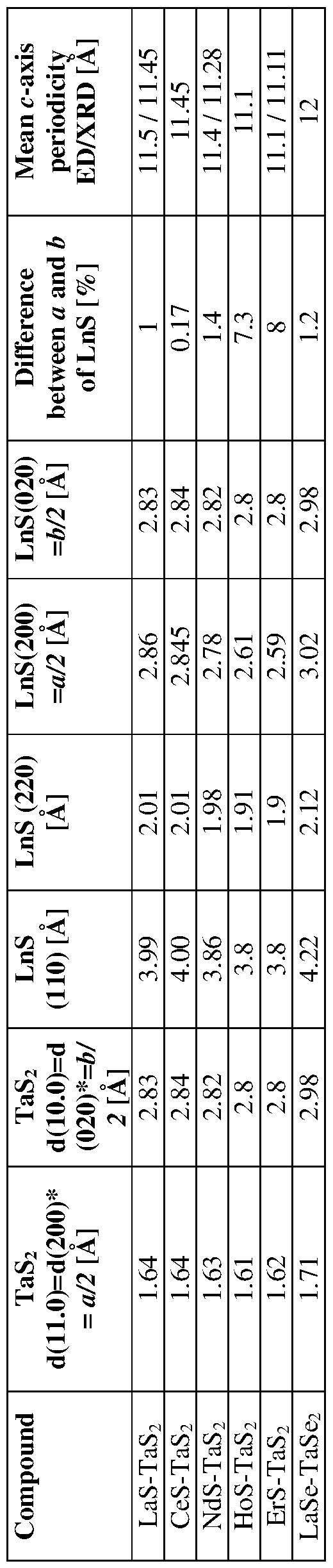
[00208] The in-plane and c-axis lattice constants of tubular structures of the LnS-TaS2 MLC are smaller than those of their MS-TaS2 (M=Sn,Pb) counterparts. Since the Ln atoms prefer a trivalent state, while Pb and Sn are divalent, charge transfer from the LnS layers to the TaS2 layers is expected to be greater than for PbS or SnS. BiS and SbS can be considered as an intermediate case. Most of the Sb and Bi atoms in SbS and BiS are believed to be trivalent just as in their well- known bulk compounds Sb2S3 and B12S3 respectively. Strong charge transfer may result in a stronger electrostatic interaction between the LnS and TaS2 layers, and consequently shorter bond lengths between the Ln and S atoms of the TaS2 layer, i.e., smaller periodicity values along the c-axis (see Figure 18).
[00209] Presumably, charge transfer between the two sublattices is responsible for the abundance of LnS-TaS2 tubules that have a single folding vector in these samples. Despite the crystallographic equivalence of the 60° rotation of the LnS relative to the TaS2 layer (see Figure 20), their orientations relative to the tubule axis are different. Obviously, only one (out of the three equivalent) common b axes between the LnS and TaS2 of the LnS-TaS2 slab can coincide with the nanotube axis (see Figure 20). Therefore, the ¾-axis of only one LnS layer (out of three) will coincide with the tubule axis. The energy associated with folding is believed to be minimal for the LnS layer, whose b-axis coincides with the tubule axis. Since the coupling between the layers is strong, it is believed that LnS-TaS2 slabs without these rotational variants can be transformed more easily into nanotubes. This situation is obviously not the case for, e.g., MS-TS2 (M= Pb;
T=Nb, Ta) tubules, in which the interlayer interaction is not as strong and tubules with three folding vectors for the MS layers and two folding vectors for the TS2 layers are produced.
[00210] Table 2 and Figure 18 show that both the average interplanar periodicity along the c-axis corresponding to the LnS-TaS2 (1 :1) superstructure and the in-plane interplanar spacings decrease with increasing atomic number of Ln (i.e., La, Ce, Nd, Ho, Er). Similar behavior was observed for bulk single crystals of LnS-TaS2 MLC and for tubular structures of MLC that are based on LnS-CrS2- This trend can be attributed to a decrease in the size of the Ln+3 ion with increasing atomic number. Similarly, the greater values of c-axis periodicity in LaSe-TaSe2, when compared to that in isostructural LaS-TaS2, can be attributed to the larger ionic radius of Se and the more covalent nature of its bonding with the metal atoms.
[00211] Based on the density of states (DOS) of the isolated LaS and NbS2 sublayers (see Figure 28), it is evident that the d states of La and Nb dominate the DOS near the respective Fermi energies. Furthermore, the Fermi energy of 5S2 is slightly below that of LaS. For this reason, as well as due to the fact that both isolated subsystems show metallic behavior, electron transfer from La to Nb in the combined system is expected.
[00212] Raman spectroscopy measurements were carried-out on single LaS- TaS2 and NdS-TaS2 tubular crystals of 200-500 nm thickness and on a 2H-TaS2 platelet. The spectra shown in Figure 19 are in agreement with their bulk counterparts.
[00213] The large upshift of the E2g mode of TaS2 relative to the bulk 2H-TaS2 is attributed to charge transfer from the LnS to the TaS2 layers which occurs in these compounds.
[00214] Nanotubular structures were formed from LnS-TaS2 (Ln=La, Ce, Nd, Ho, Er) and LaSe-TaSe2 MLC in evacuated silica tubes when subjected to appropriate temperature profiles and growth times. The compounds were found to be commensurate along the b-axis and incommensurate along the a-axis. SAED patterns of the tubes suggest a single folding vector for the LnS and TaS2 layers in most cases. As expected, the commensurate b-axes of the LnS and TS2 layers coincide with the tubule axis.
[00215] The mutual structural modulation of the TaS2 and LnS lattices results in an orthorhombic distortion of the rocksalt LnS lattice, while the TaS2 is barely modified. The difference between the in-plane lattice parameters (a and b) of LnS in LnS-TaS2 MLC became more significant for HoS and ErS, than for LaS, LaSe, CeS and NdS. Both the c-axis periodicity of the LnS-TaS2 superstructure and the in-plane lattice periodicities of the LnS and TaS2 layers decrease with increasing atomic number of Ln. The periodicity is greater for selenides than for corresponding sulfides.
[00216] The smaller periodicities in the LnS-TaS2 tubules relative to their SnS- TaS2 and PbS-TaS2 counterparts indicate a stronger interaction between the two subsystems for the former. Such an observation is supported by a high upshift in the Z¾g Raman mode of TaS2 in these compounds. Theoretical calculations for LaS-NbS2 confirm the structural modulation obtained by the coupling of the two
subsystems and indicate a small net charge transfer from the LaS layer to the hexagonal sublattice.
Chemical analysis of the products
[00217] Representative examples of EDS analysis of the synthesized LnS-TaS2 tubes are shown in Figure 21. A spectrum recorded from a LaSe-TaSe2 tubule produced by the addition of TaBrs powder to the ampoule is also shown. Chlorine peaks are clearly visible in the EDS spectra of LnS-TaS2 and bromine is visible for LaSe-TaSe2 nanotubes, as shown in Figure 21. EDS analysis of LnS-TaS2 nanotubes with (Ln=La,Ce, Nd) indicated the presence of 1-2 at% CI (Figure 21). However, no clear CI peak could be detected for Ln=Ho and Er MLC nanotubes. A Br peak was clearly visible in EDS spectra recorded from LaSe-TaSe2 nanotubes (Figure 21g).
[00218] Table 3. Typical outer diameters of the LnX-TaX2 tubular structures.

[00219] Tubular structures from LnS-TaS2 (Ln=Ce, Nd, Ho, Er) and LaSe-TaSe2 MLC with a single folding vector of LnS(Se) and TaS2(Se)
[00220] The in-plane lattice parameters a and b of LnS(Se) and TaS2(Se)
(labeled according to the ortho-pseudohexagonal system) were calculated from the (10.0) and (11.0) reflections of TaS2 and the (220) reflections of LnS and are summarized in Table 1. The ¾-axis is commensurate and common to both the LnS and the TaS2 and was assumed to be equal for the calculations.
[00221] Tubular structures from ErS-TaS2 and LaSe-TaSe2 MLC with a single folding vector of LnS(Se) and TaS2(Se)
[00222] SAED patterns acquired from ErS-TaS2 and LaSe-TaSe2 tubules are shown in Figures 24a(a) and 24a(b). The tubules are, in principle, isostructural to that shown in Figure 17c for LaS-TaS2 counterpart except for the following:
[00223] For ErS-TaS2, it is apparent that the 200 spots of ErS (marked by segmented ellipses) are "shifted" slightly away from the dashed circles that correspond to the 10.0 spots of TaS2 and the 020 spots of ErS. This shift is indicative of the presence of a slightly smaller interplanar a-spacing, when compared to the ^-spacing of the ErS layer (Fig. 24b). Therefore, in this case the difference between the in-plane lattice parameters (a and b) of LnS (i.e., ErS) is more apparent. Such a shift is also apparent for HoS-TaS2 tubular structures (Fig. 25(b)), but not for LaS-TaS2 (Figure 17), CeS-TaS2 (Figure 26a), NdS-TaS2 (Figure 25(a))or LaSe-TaSe2 (Figure 24(b)). The in-plane lattice parameters {a and b) of LnS and TaS2 (labeled according to the ortho-pseudohexagonal system) were calculated from the (10.0) and (11.0) reflections of TaS2(Se) and from the (220) reflections of LnS(Se). The results are summarized in Table 1. For the LaSe-TaSe2 tubule shown in Figure S5b, the lattice periodicities are significantly larger than for the LaS-TaS2 counterpart.
[00224] Table 4. Literature values of the interplanar spacings of TaS2 and LnS. * The (11.0) and (10.0) planes, according to the pseudohexagonal system of labeling for TaS2, are equivalent to the (200) and (020) planes, respectively, according to the ortho-pseudohexagonal system.


Raman spectra of single LaS-TaS2 and NdS-TaS2 nanotubes
[00225] Representative Raman spectra recorded from single tubular nanocrystals of LaS-TaS2 and NdS-TaS2 are shown in Figure 19. The spectra recorded from LaS-TaS2 are in excellent agreement with results published previously for a bulk single crystal.
[00226] The spectra recorded from NdS-TaS2 tubular crystals are quite similar to their LaS-TaS2 counterparts. However, no previous literature data could be found for NdS-TaS2- Inasmuch as spectra recorded from bulk LnS-TaS2 MLC
with (Ln=La, Ce, Sm and Gd) were found to be similar, the similarity of NdS- TaS2 is not surprising.
[00227] The mode at 400 cm"1 is in perfect agreement with the A\g (intralayer out-of-plane vibration) mode of 2H-TaS2- The mode at 327 cm4 is attributed to the Z¾g (intralayer in-plane vibration) mode, which occurs at 286 cm"1 in bulk 2H- TaS2- The large upshift of the intralayer Z¾g mode of the TaS2 layer (41 cm"1 in this case) has been reported for various intercalation compounds of 2H-TaS2 (and 2H-NbS2), including the misfit compounds.
[00228] The mode at -149 cm"1 matches the A\g (intralayer out-of-plane vibration) mode at 148 cm"1 of LaS in a LaS-TaS2 MLC single crystal. An additional A\g mode at 122 cm"1 was previously observed, but was not observed here due to experimental limitations at lower wavenumbers. The observed Raman modes of the LaS layers within LaS-TaS2 MLC are different from the modes observed in LaS bulk single crystals with NaCl structure. The broad band between ~ 240 and 303 cm"1 is attributed to the two-phonon band.
[00229] The differences between the Raman modes of pristine bulk LnS and TaS2 and the modes observed in the corresponding MLC can be interpreted in terms of charge transfer from the LnS to the TaS2 layers. Charge transfer increases both the intralayer and the interlayer interaction between the layers, thereby affecting the Raman frequencies. In addition, the Raman spectra are expected to be affected by the mutual structural modulation. Recall that the structure of the LnS layers (and to a lesser extent that of the TaS2 layers) within the MLC is slightly different from bulk LnS with a NaCl structure.
EXAMPLE 3
Synthesis of Tubular Structures from the LnS-TaS2 (Ln=La, Ce, Nd, Ho, Er) and LaSe-TaSe2 Misfit Layered Compounds
[00230] The synthesis of LnS-TaS2 (Ln=La, Ce, Nd, Ho, Er) and LaSe-TaSe2 MLC tubular structures was carried out in evacuated ampoules at a vacuum of ~ 5x10~5 torr. Ta, Ln, S or Se powders were taken at molar ratios of -1 :1 :3. Small amounts of Ta(¾ or TaBr5 powder were added as a CI/Br source. CI/Br is believed to act as a transport agent. After sealing, the ampoules were held in a vertical furnace and two annealing steps were performed. First, the ampoules were held in a temperature gradient of 400 °C at the bottom (with the precursors) and 850 °C at the upper part for 1 hr. In the second step, the temperatures were tuned to 850 °C at the bottom (with the precursors) and 50 °C at the upper part. This step lasted for 4 -16 hr. Most of the product remained at the hot edge of the ampoules. The amount of the substance transported to the cold edge was negligible.
Electron microscopy, XRD, Raman spectroscopy
[00231] After the ampoules were opened, the powder products from the hot zone were examined by SEM, HRTEM, STEM, XRD, and Raman spectroscopy.
[00232] X-ray diffraction (XRD) patterns were recorded with a Rigaku TTRAXIII diffractometer (Cu-Κα radiation) operating in the Bragg-Brentano (Θ- 2Θ) mode.
[00233] For SEM analysis, small amount of powder was put on C tape stuck to an Al stub. The resulting samples were examined using a Zeiss Ultra model V55
SEM and a LEO model Supra 55VP SEM equipped with an EDS detector (Oxford model INCA).
[00234] For high-resolution transmission electron microscopy (HRTEM) a solution of the product in ethanol was dripped onto a lacey/holey carbon/collodion-coated Cu grids. The resulting samples were examined by Philips CM120 TEM, operating at 120 kV equipped with EDS detector (EDAX- Phoenix Microanalyzer); JEOL JEM2100 operating at 200 kV and FEI Tecnai F30-UT HRTEM operating at 300 kV. High-resolution scanning transmission electron microscopy (STEM) images and EDS chemical maps were taken on a probe-corrected FEI Titan 80-200 G2 ChemiSTEM instrument equipped with a Bruker Super-X detector at 200 kV.
[00235] For Raman spectroscopy measurements, droplets of an ethanol solution containing the product were dripped on Si wafers. Raman measurements were carried out using a Renishaw Micro Raman In Via Imaging Microscope equipped with a CCD device. Tubes with diameters of 0.2-1 μπι could easily be discerned using the light microscope. A He-Ne laser (λ=633) nm was used for excitation.
EXAMPLE 4
Synthesis of meta-stable compounds in stable form on top oflanthanide based misfit compounds and studying their electronic properties: The case of chromium disulfide nanotubes and chromium diselenide nanotubes
(CrS?.@LaCrSi and CrSe7@LaCrS,.rSer)
[00236] LaS intercalated CrS2 (LaCrSs) nanotubes were synthesized by sulfurization of La(OHte and Cr(OHb mixture at high temperature. Figure 30
shows the SEM (a and b) and TEM (c) image of typical LaCrS3 nanotubes. This material show one-to-one stacking order of the LaS-CrS2 superstructure which is necessary for securing the stability of the hexagonal layered structure of the CrS2- As previously noted, the general formula (LaCrSs) is equivalent to the formula [(M1X'(p)X"(1-p))i+z(M2X,(q)X"(i-q))y](TX'(k)X"(2-k)), wherein M1=La, X'=S, T=Cr, y=0, p=l, k=2 and 1+z is omitted for clarity.
[00237] Increasing Cr stoichiometry in precursor while synthesizing LaCrS3 nanotubes, allowed the formation of CrS2 nanotubes without intercalation over the top of LaCrS3 nanotubes (unpublished). Figure 31 a and b respectively show SEM and TEM images of GS2 nanotubes on top of LaCrS3 nanotubes. Line profile in bottom of Fig. 31b clearly show the presence of CrS2 layers on top of LaCrS3 nanotube. Preliminary data on CrS2 coated LaCrS3 nanotube showed substantial increase in conductivity (about 3 orders of magnitude) compared to LaCrS3 nanotubes. Se substituted LaCrS3 nanotubes also found to show higher conductivity (about 3 orders of magnitude).
[00238] Table 6 summarizes the new nanotubes which were synthesized. Table 6: Nanotubes and synthesis techniques

Synthesis
[00239] Synthesis of Se substituted LaCrS3 nanotubes [LaSi-xSex-Cr(Si-xSex)2 or (LaCrS3_xSex)] : Mixture of LaCrS3 nanotubes mixed with selenium powder with 1:1 ratio in a quartz ampoule. The ampoule vacuum sealed at ~10~5 torr and reaction mixture is subjected heat at different temperatures (700 °C to 850 °C) and maintained other end 50 °C higher than reaction temperature. The reaction duration is varied from 6 to 24 h. In optimized conditions, 40 at% of S is substituted with Se.
[00240] Synthesis of CrS2 nanotubes on top of LaCrS3 nanotubes [CrS2@LaCrS3] : mixture of La(OH)3 and Cr(OH)3 1:1.1 mole ration was subjected to anneal at 900 °C for 2h in the presence of 40 seem (standard cubic centimeter per minute) of 5% ¾+95 N2 and 5 seem H2S.
[00241] Synthesis of CrSe2@LaCrS3_xSex nanotubes: The above product, CrS2@LaCrS3, was mixed with Se powder with 1 :1 ratio in a quartz ampoule. The ampoule vacuum sealed at ~10~5 torr and reaction mixture is subjected heat at 800 °C and maintained other end at 850 °C for 12h.
EXAMPLE 5
Synthesis ofLaSrSei.r - TaSvSe tubular structures
[00242] LaSxSei_x - TaSySe2-y tubular structures were synthesized. The tubular structures were produced in two ways:
[00243] 1. Powder of the preformed LaS-TaS2 tubular structures was mixed with Ta, La, Se and TaCls powders and sealed in a silica tube. The thermal treatment was similar to the described in the experimental part.
[00244] 2. Ta, La, S, Se and TaCls powders were mixed and sealed in a silica tube.
[00245] The thermal treatment was similar to the treatment described in the experimental part herein below.
[00246] Experimental Section
[00247] Synthesis of the tubular structures
[00248] The synthesis of LnS-TaS2 (Ln=La, Ce, Nd, Ho, Er) and LaSe-TaSe2 MLC tubular structures was carried out in evacuated ampoules at a vacuum of ~ 5x10"5 torr. Ta, Ln, S or Se powders were taken at molar ratios of -1 :1 :3. Small amounts of TaCls or TaBrs powder were added as a CI/Br source. CI/Br is believed to act as a transport agent. After sealing, the ampoules were held in a vertical furnace and two annealing steps were performed. First, the ampoules were held in a temperature gradient of 400 °C at the bottom (with the precursors) and 850 °C at the upper part for 1 hr. In the second step, the temperatures were tuned to 850 °C at the bottom (with the precursors) and 50 °C at the upper part. This step lasted for 4 -16 hr. Most of the product remained at the hot edge of the ampoules. The amount of the substance transported to the cold edge was negligible.
[00249] LaSxSei_x - TaSySe2-y tubular structures:
[00250] LaSxSei_x - TaSySe2-y tubular structures could be produced as well. These could be produced in two ways:
[00251] 1. Powder of the preformed LaS-TaS2 tubular structures (as described in the experimental part herein above) was mixed with Ta, La, Se and TaCls powders and sealed in a silica tube. The thermal treatment is similar to the described in the experimental part herein above.
[00252] 2. Ta, La, S, Se and TaCls powders were mixed and sealed in a silica tube.
[00253] The thermal treatment is similar to the described in the experimental part herein above.
[00254] Figure 29: LaSxSei_x - TaSySe2-y tubular structures, (a) SEM image, (b) High magnification TEM image of a single LaSxSei_x - TaSySe2-y nanotube, with LaSxSei_x and TaSySe2-y layers stacked in an alternating sequence with 1.16 nm periodicity along the common c-axis. The insets are low magnification image and line profile integrated along the rectangle marked in the high magnification image.
[00255] While certain features of the invention have been illustrated and described herein, many modifications, substitutions, changes, and equivalents will now occur to those of ordinary skill in the art. It is, therefore, to be understood that the appended claims are intended to cover all such modifications and changes as fall within the true spirit of the invention.
Claims
1. A nanomaterial of formula

wherein Mi being a metal, M2 being a metal, T being a transition metal, each of X' and X" being independently S or Se, 0< <0.2, 0<z<0.3, 0<p<l , 0≤q≤l, 0≤k<2, and M≠M2, provided that when y is zero than ζ , and when z is zero than y≠0.
2. The nanomaterial of claim 1, wherein said nanomaterial being of the formula [(MiX')i+z(M2X')y](TX"2), wherein Mi being a lanthanide metal, M2 being a metal, T being a transition metal, each of X' and X" being independently S or Se, 0<y<0.2, 0<z<0.3, and Mi≠M2, provided that when y is zero than ζ , and when z is zero than y≠ .
3. The nanomaterial of claims 1 or 2, wherein Mi is selected from La, Ce, Pr, Nd, Pm, Sm, Eu, Gd, Tb, Dy, Ho, Er, Tm, Yb, Lu, or Y.
4. The nanomaterial of claims 1 or 2, wherein Mi is selected from La, Ce, Gd, Tb or Y.
5. The nanomaterial of any one of claims 1 to 4, wherein M2 is selected from Ca, Sr, Ba, Y, La, Ce, Pr, Nd, Pm, Sm, Eu, Gd, Tb, Dy, Ho, Er, Tm, Yb, or Lu.
6. The nanomaterial of any one of claims 1 to 5, wherein T is selected from Ti, V, Cr, Mn, Fe, Co, Ni, Nb, Ta, W or Mo.
7. The nanomaterial of any one of claims 1 to 6, being of the formula (LaS)i+zCrS2, (LaS)i+zVS2, (CeS)i+zCrS2, (CeS)i+zVS2, (GdS)i+zCrS2, (GdS)i+zVS2, wherein 0<z<0.3.
8. The nanomaterial of any one of claims 1 to 6, being of the formula LaS(SrS)yCrS2, LaS(SrS)yVS2, LaS(CeS)yCrS2, LaS(CeS)yVS2, LaS(GdS)yCrS2, LaS(GdS)yVS2, CeS(SrS)yCrS2, CeS(SrS)yVS2, CeS(GdS)yCrS2, CeS(GdS)yVS2, LaS(EuS)yCrS2, wherein 0<y<0.2.
9. The nanomaterial of claim 1, wherein said nanomaterial being of the formula selected from LaSpSei_p-TaSkSe2-k. or LaSi_pSep-Cr(S2-kSek)2 or LaCrS3_xSex covered by 1-5 layers of CrSe2.
10. The nanomaterial of any one of claims 1 to 8, being a layered nanomaterial.
11. The nanomaterial of claim 9, comprising at least one first layer having the formula [(MiX')i+z(M2X')y] and at least one second layer having the formula (TX'y.
12. The nanomaterial of claim 10, being of the formula [(MiX')i+z(M2X')y]m(TX"2)n, wherein m and n being integers, independently selected from 1 to 10.
13. The nanomaterial of claim 11 , wherein each of m and n is independently selected from 1 to 3.
14. The nanomaterial of any one of claims 10 to 12, wherein said first layers and said second layers are alternately stacked.
15. The nanomaterial of any one of claims 1 to 13, being selected from a sheet, a distorted sheet, a fullerene-like nanostructure or a tubular nanostructure.
16. The nanomaterial of claim 14, wherein said tubular nanostructure is selected from a nanotube and a nanoscroll.
17. The nanomaterial of claim 15, wherein the diameter of said tubular nanostructure is between about 20 and about 500 nm.
18. The nanomaterial of claim 16, wherein the diameter of said tubular nanostructure is between about 20 and about 300 nm.
19. A layered nanostructure comprising at least one first layer having the formula [(MiX'(P)X"(i_p))i+z(M2X'(q)X"(i-q))y]m and at least one second layer having the formula (TX'(k X"(2-k))n, wherein Mi being a metal, M2 being a metal, T being a transition metal, each of X' and X" being independently S or Se, 0<p<l, 0¾<1 , 0≤k<2, 0≤y≤D.2, 0<z<0.3, m and n being integers, independently selected from 1 to 10, and Mi≠M2, provided that when y is zero than ζ , and when z is zero than y≠0 .
20. A layered nanostructure comprising at least one first layer having the formula
[(MiX')i+z(M2X')y]m and at least one second layer having the formula (TX"2)n, wherein
Mi being a lanthanide metal, M2 being a metal, T being a transition metal, each of X'
and X" being independently S or Se, 0<y<0.2, 0<z<0.3, m and n being integers, independently selected from 1 to 10, and Mi≠M2, provided that when y is zero than ζ , and when z is zero than y≠0 .
21. The layered nanostructure of claims 18 or 19, wherein Mi is selected from La, Ce, Pr, Nd, Pm, Sm, Eu, Gd, Tb, Dy, Ho, Er, Tm, Yb, Lu, or Y.
22. The layered nanostructure of claim 18 or 19, wherein M2 is selected from Ca, Sr, Ba, Y, La, Ce, Pr, Nd, Pm, Sm, Eu, Gd, Tb, Dy, Ho, Er, Tm, Yb, or Lu.
23. The layered nanostructure of any one of claims 18 to 20, wherein T is selected from Ti, V, Cr, Mn, Fe, Co, Ni, Nb, Ta, W or Mo.
24. The layered nanostructure of any one of claims 18 to 21, wherein m and n are the same.
25. The layered nanostructure of claim 21 , wherein both m and n are 1.
26. The layered nanostructure of any one of claims 18 to 21 , wherein m is 2n.
27. The layered nanostructure of any one of claims 18 to 21, wherein said nanostructure comprises a plurality of said first layer and a plurality of said second layer.
28. The layered nanostructure of claim 25, wherein said first layers and said second layers are alternately stacked.
29. The layered nanostructure of any one of claims 18 to 26, being selected from a sheet, a distorted sheet, a fullerene-like nanostructure or a tubular nanostructure.
30. The layered nanostructure of claim 27, wherein said tubular nanostructure is selected from a nanotube and a nanoscroll.
31. The layered nanostructure of claim 28, wherein the diameter of said tubular nanostructure is between about 20 and about 500 nm.
32. The layered nanostructure of claim 29, wherein the diameter of said tubular nanostructure is between about 20 and about 300 nm.
33. A layered nanostructure comprising a plurality of superlayers, each superlayer in said plurality of superlayers being composed of a first sublayer of the formula
[(MiX')i+z(M2X')y]m and a second sublayer of formula (TX"2)n, said plurality of superlayers being stacked, wherein Mi being a lanthanide metal, M2 being a metal, T being a transition metal, each of X' and X" being independently S or Se, 0<y<0.2, 0<z<0.3, and Mi≠M2, provided that when y is zero than ζ , and when z is zero than y≠ .
34. The layered nanostructure of claim 32, wherein said plurality of superlayers comprises between 2 and 100 superlayers.
35. The layered nanostructure of claim 32, wherein said plurality of superlayers comprises between 2 and 20 superlayers.
36. The layered nanostructure of any one of claims 32 to 34, wherein Mi is selected from La, Ce, Pr, Nd, Pm, Sm, Eu, Gd, Tb, Dy, Ho, Er, Tm, Yb, Lu, or Y.
37. The layered nanostructure of any one of claims 32 to 35, wherein M2 is selected from Ca, Sr, Ba, Y, La, Ce, Pr, Nd, Pm, Sm, Eu, Gd, Tb, Dy, Ho, Er, Tm, Yb, or Lu.
38. The layered nanostructure of any one of claims 32 to 36, wherein T is selected from Ti, V, Cr, Mn, Fe, Co, Ni, Nb, Ta, W or Mo.
39. The layered nanostructure of any one of claims 32 to 36, being selected from a sheet, a distorted sheet, a fullerene-like nanostructure or a tubular nanostructure.
40. The layered nanostructure of claim 38, wherein said tubular nanostructure is selected from a nanotube and a nanoscroll, and the diameter of said tubular nanostructure is between about 20 and about 500 nm.
41. A layered nanostructure comprising at least one first layer of the formula [(MiX'(p)X"(i-p))i+z(M2X'(q)X"(i-q))y], having a first crystallographic cell unit, and at least one second layer of formula (TX'(k)X"(2-k)), having a second crystallographic cell unit, said first and second layers being alternately stacked, wherein said first and second crystallographic cell units having a misfit defined by the ratio {ai-a2/ai) having a value of between 0.3 and 0.5, wherein Mi being a metal, M2 being a metal, T being a transition metal, each of X' and X" being independently S or Se, 0<p<l , 0≤q≤l, 0≤k<2, 0<y<0.2, 0<z<0.3, and Mi≠M2, provided that when y is zero than ζ , and when z is zero than y≠0.
42. A layered nanostructure comprising at least one first layer of the formula [(MiX')i+z(M2X')y] having a first crystallographic cell unit, and at least one second layer of formula TXM2 having a second crystallographic cell unit, said first and second layers being alternately stacked, wherein said first and second crystallographic cell units having a misfit defined by the ratio (07-02 0;) having a value of between 0.3 and 0.5, wherein Mi being a lanthanide metal, M2 being a metal, T being a transition metal, each of X' and X" being independently S or Se, 0< <0.2, 0<z<0.3, and Mi≠M2, provided that when y is zero than ζ , and when z is zero than y≠0
43. The layered nanostructure of any one of claims 19 to 41, being of the formula (LaS)i+zCrS2, (LaS)i+zVS2, (CeS)i+zCrS2, (CeS)i+zVS2, (GdS)i+zCrS2, (GdS)i+zVS2, wherein 0<z<0.3.
44. The layered nanostructure of any one of claims 19 to 41, being of the formula LaS(SrS)yCrS2, LaS(SrS)yVS2, LaS(CeS)yCrS2, LaS(CeS)yVS2, LaS(GdS)yCrS2, LaS(GdS)yVS2, CeS(SrS)yCrS2, CeS(SrS)yVS2, CeS(GdS)yCrS2, CeS(GdS)yVS2, LaS(EuS)yCrS2, wherein 0<y<0.2.
45. A process for obtaining a nanomaterial of the formula [(MiX'(P)X"(i_ p))i+z(M2X'(q)X"(i_q))y](TX'(k)X"(2-k))„ wherein Mx being a metal, M2 being a metal, T being a transition metal, each of X' and X" being independently S or Se, 0≤p≤l, 0≤q≤l, 0<k<2, 0< <0.2, 0<z<0.3, m and n being integers, independently selected from 1 to 10, and Mi≠M2, provided that when y is zero than ζ , and when z is zero than y≠0, the process comprising:
(i) providing a substrate comprising Mi-precursor, T-precursor and optionally M2 precursor;
(ii) heating said substrate to elevated temperature at a heating rate of at least 10 °C/min; and
(iii) contacting said substrate with H2/N2 gas mixture and H2S gas at said elevated temperature for a period of time permitting obtaining said nanomaterial.
46. A process for obtaining a nanomaterial of the formula [(MiX')i+z(M2X)'y]m(TX"2)n, wherein Mx being a lanthanide metal, M2 being a metal, T being a transition metal, each of X' and X" being independently S or Se, 0<y<0.2,
0<z<0.3, m and n being integers, independently selected from 1 to 10, and Mi≠M2, provided that when y is zero than ζ , and when z is zero than y≠0, the process comprising:
(i) providing a substrate comprising Mi-precursor, T-precursor and optionally M2 precursor;
(ii) heating said substrate to elevated temperature at a heating rate of at least 10 °C/min; and
(iii) contacting said substrate with H2/N2 gas mixture and ¾S gas at said elevated temperature for a period of time permitting obtaining said nanomaterial.
47. The process of claims 44 or 45, wherein said nanomaterial is a layered nanostructure, comprising at least one first layer having the formula [(MiX')i+z(M2X)'y]m and at least one second layer having the formula (TX"2)n.
48. The process of claim 44 to 46, wherein said Mi-precursor, T-precursor and M2 precursor are oxides or hydroxides of Mi, M2 and T, respectively.
49. The process of any one of claims 41 to 43, wherein the T-precursor is used in molar excess to the Mi -precursor.
50. The process of any one of claims 44 to 47, wherein the ratio (mol/mol) between Mi-precursor and T-precursor is 1 :1.
51. The process of any one of claims 44 to 47, wherein the ratio (mol/mol) between Mi-precursor and M2-precursor, when present, is at most 1 :0.2.
52. The process of any one of claims 44 to 50, wherein said elevated temperature is between about 800 and 1200°C.
53. The process of claim 51, wherein said elevated temperature is between about 800 to 950°C.
54. The process of any one of claims 44 to 52, wherein said heating rate is between about 10 and 20 °C/min.
55. The process of claim 53, wherein said heating rate is between about 12 and 18 °C/min.
56. The process of any one of claims 44 to 54, wherein the volumetric ratio between said H2/N2 gas mixture and said H2S gas is between about 8:1 and 6: 1.
57. The process of any one of claims 44 to 55, wherein said period of time is between about 5 minutes and 2 hours.
58. The process of any one of claims 44 to 56, wherein said substrate is in the form of a slab, a block, a particle, a flake, a powder, or a nano whisker.
59. The process of any one of claims 44 to 58, wherein Mi is selected from La, Ce, Pr, Nd, Pm, Sm, Eu, Gd, Tb, Dy, Ho, Er, Tm, Yb, Lu, or Y.
60. The process of any one of claims 44 to 58, wherein M2, when present, is selected from Ca, Sr, Ba, Y, La, Ce, Pr, Nd, Pm, Sm, Eu, Gd, Tb, Dy, Ho, Er, Tm, Yb, or Lu.
61. The process of any one of claims 44 to 59, wherein T is selected from Ti, V, Cr, Mn, Fe, Co, Ni, Nb, Ta, W or Mo.
62. The process of any one of claims 44 to 60, wherein said nanomaterial being a nanostructure selected from a sheet, a distorted sheet, a fullerene-like structure or a tubular nanostructure.
63. The process of claim 61 , wherein said tubular nanostructure is selected from a nanotube and a nanoscroll.
64. The process of claim 62, wherein the diameter of said tubular nanostructure is between about 20 and about 500 nm.
65. A nanomaterial of the formula [(MiX'(P)X''(i-p))i*-(M2X,(q)X''(i-q))y]( X,a-)X"(2-k))» wherein Mi being a metal, M2 being a metal, T being a transition metal, each of X' and X" being independently S or Se, 0<y<0.2, 0<z<0.3, 0<p<l , 0≤q≤l , 0≤k<2, m and n being integers, independently selected from 1 to 10, and Mi≠M2, provided that when y is zero than ζ , and when z is zero than y≠0, obtainable by the process of any one of claims 44 to 63.
66. A nanomaterial of the formula [(MiX')i+z(M2X')y]m(TX"2)n, wherein Mi being a lanthanide metal, M2 being a metal, T being a transition metal, each of X' and X" being independently S or Se, 0<y<0.2, 0<z<0.3, m and n being integers, independently
selected from 1 to 10, and Mi≠M2, provided that when y is zero than ζφ , and when z is zero than y≠0, obtainable by the process of any one of claims 44 to 63.
67. A composition comprising the nanomaterial of any one of claims 1 to 16 or the layered nanostructure of any one of claims 17 to 40.
68. The composition of claim 61 , being selected from a lubricant composition, a shock absorbing composition, nanostructured electrical conductor, additives composition to lubricating fluids, a self-lubricating coating composition, and coatings.
69. An article comprising the nanomaterial of any one of claims 1 to 17 or the layered nanostructure of any one of claims 18 to 43.
70. The article of claim 68, wherein said article being selected from a thermoelectric component, a transistor, a solar cell, an electrode, and photo-catalyst.
Applications Claiming Priority (2)
| Application Number | Priority Date | Filing Date | Title |
|---|---|---|---|
| US201461989859P | 2014-05-07 | 2014-05-07 | |
| US61/989,859 | 2014-05-07 |
Publications (2)
| Publication Number | Publication Date |
|---|---|
| WO2015170331A2 true WO2015170331A2 (en) | 2015-11-12 |
| WO2015170331A3 WO2015170331A3 (en) | 2015-12-30 |
Family
ID=53900883
Family Applications (1)
| Application Number | Title | Priority Date | Filing Date |
|---|---|---|---|
| PCT/IL2015/050479 Ceased WO2015170331A2 (en) | 2014-05-07 | 2015-05-07 | Inorganic nanomaterials |
Country Status (1)
| Country | Link |
|---|---|
| WO (1) | WO2015170331A2 (en) |
Cited By (3)
| Publication number | Priority date | Publication date | Assignee | Title |
|---|---|---|---|---|
| US20230226536A1 (en) * | 2020-06-10 | 2023-07-20 | Max Planck Gesellschaft Zur Förderung Der Wissenschaften eV | Selection of a heterogeneous catalysts with metallic surface states |
| US11859080B2 (en) | 2018-02-22 | 2024-01-02 | Yeda Research And Development Co. Ltd. | Hydroxyapatite based composites and films thereof |
| US12365794B2 (en) | 2018-12-27 | 2025-07-22 | Yeda Research And Development Co. Ltd. | Nanocomposites comprising biodegradable polymers and inorganic nanoparticles, methods of preparation and uses thereof |
Family Cites Families (2)
| Publication number | Priority date | Publication date | Assignee | Title |
|---|---|---|---|---|
| US8545991B2 (en) * | 2009-01-23 | 2013-10-01 | State Of Oregon Acting By And Through The State Board Of Higher Education On Behalf Of The University Of Oregon | Low thermal conductivity misfit layer compounds with layer to layer disorder |
| US20140287264A1 (en) * | 2011-10-20 | 2014-09-25 | Yeda Research And Development Co. Ltd. | Ordered stacked sheets of layered inorganic compounds, nanostructures comprising them, processes for their preparation and uses thereof |
-
2015
- 2015-05-07 WO PCT/IL2015/050479 patent/WO2015170331A2/en not_active Ceased
Non-Patent Citations (1)
| Title |
|---|
| None |
Cited By (3)
| Publication number | Priority date | Publication date | Assignee | Title |
|---|---|---|---|---|
| US11859080B2 (en) | 2018-02-22 | 2024-01-02 | Yeda Research And Development Co. Ltd. | Hydroxyapatite based composites and films thereof |
| US12365794B2 (en) | 2018-12-27 | 2025-07-22 | Yeda Research And Development Co. Ltd. | Nanocomposites comprising biodegradable polymers and inorganic nanoparticles, methods of preparation and uses thereof |
| US20230226536A1 (en) * | 2020-06-10 | 2023-07-20 | Max Planck Gesellschaft Zur Förderung Der Wissenschaften eV | Selection of a heterogeneous catalysts with metallic surface states |
Also Published As
| Publication number | Publication date |
|---|---|
| WO2015170331A3 (en) | 2015-12-30 |
Similar Documents
| Publication | Publication Date | Title |
|---|---|---|
| Wang et al. | Recent advances in ternary two-dimensional materials: synthesis, properties and applications | |
| Mahour et al. | Structural, optical and Mössbauer spectroscopic investigations on the environment of Fe in Fe-doped ZnO (Zn1-xFexO) ceramics synthesized by solution combustion method | |
| Liu et al. | Synthesis and characterization of nanocrystalline niobates | |
| Bokhimi et al. | Dependence of boehmite thermal evolution on its atom bond lengths and crystallite size | |
| Kiruthigaa et al. | Structural, optical and photocatalytic properties of Ce-doped SnS2 nanoflakes | |
| Shi et al. | Synthesis and structure of two-dimensional transition-metal dichalcogenides | |
| Zhao et al. | Two-dimensional tantalum disulfide: controlling structure and properties via synthesis | |
| Nikonov et al. | Chemical vapor transport growth of vanadium (IV) selenide and vanadium (IV) telluride single crystals | |
| Liu | Low temperature synthesis of hexagonal phase ZnS nanocrystals by thermolysis of an air-stable single-source molecular precursor in air | |
| Pereira et al. | Influence of doping on the preferential growth of α-MoO3 | |
| Zhang et al. | Phase-controlled synthesis of ZnS nanocrystallites by mild solvothermal decomposition of an air-stable single-source molecular precursor | |
| Zhuk et al. | Thermal expansion, crystal structure, XPS and NEXAFS spectra of Fe-doped bismuth tantalate pyrochlore | |
| Sarilmaz et al. | Ternary copper tungsten selenide nanosheets synthesized by a facile hot-injection method | |
| Reshmi et al. | Structural stability of coplanar 1T-2H superlattice MoS2 under high energy electron beam | |
| Tikhanova et al. | Synthesis and phase transformations of hexagonal, orthorhombic, and cubic ScxLu1-xFeO3 (0≤ x≤ 1) nanocrystals | |
| Yu et al. | A mild solvothermal route for preparation of cubic-like CuInS2 crystals | |
| Li et al. | Simple solution route to uniform MoS2 particles with randomly stacked layers | |
| Surya et al. | Phase, structural and thermodynamic analysis of nanocrystalline yttrium oxide (Y2O3) for optical applications | |
| Kususe et al. | Structural phase transitions in EuNbO3 perovskite | |
| Keereeta et al. | Revealing effect of cobalt dopant on crystallography and optical characteristics of nanostructured cupric oxide | |
| Sun et al. | Colloidal synthesis of ultrathin KFeS2 and RbFeS2 magnetic nanowires with non-van der Waals 1D structures | |
| Zhang et al. | Solvothermal synthesis of uniform hexagonal-phase ZnS nanorods using a single-source molecular precursor | |
| González-Jiménez et al. | Synthesis of 4H-SrMnO3. 0 nanoparticles from a molecular precursor and their topotactic reduction pathway identified at atomic scale | |
| Robert et al. | Tunable magnetic switching and electronic structure in Cr3+/Fe3+ Co-substituted 2D SnS2 nanosheets | |
| Cao et al. | A solvothermal crystallization route to the preparation of microsized hollow cones of quasi-2D antimony sulfide |
Legal Events
| Date | Code | Title | Description |
|---|---|---|---|
| 121 | Ep: the epo has been informed by wipo that ep was designated in this application |
Ref document number: 15753489 Country of ref document: EP Kind code of ref document: A2 |
|
| NENP | Non-entry into the national phase |
Ref country code: DE |
|
| 122 | Ep: pct application non-entry in european phase |
Ref document number: 15753489 Country of ref document: EP Kind code of ref document: A2 |