WO2015152257A1 - 化合物薄膜太陽電池、化合物薄膜太陽電池の製造方法、および、光吸収層 - Google Patents
化合物薄膜太陽電池、化合物薄膜太陽電池の製造方法、および、光吸収層 Download PDFInfo
- Publication number
- WO2015152257A1 WO2015152257A1 PCT/JP2015/060159 JP2015060159W WO2015152257A1 WO 2015152257 A1 WO2015152257 A1 WO 2015152257A1 JP 2015060159 W JP2015060159 W JP 2015060159W WO 2015152257 A1 WO2015152257 A1 WO 2015152257A1
- Authority
- WO
- WIPO (PCT)
- Prior art keywords
- coordinates
- coordinate
- ratio
- light absorption
- solar cell
- Prior art date
- Legal status (The legal status is an assumption and is not a legal conclusion. Google has not performed a legal analysis and makes no representation as to the accuracy of the status listed.)
- Ceased
Links
Images

Classifications
-
- C—CHEMISTRY; METALLURGY
- C01—INORGANIC CHEMISTRY
- C01B—NON-METALLIC ELEMENTS; COMPOUNDS THEREOF; METALLOIDS OR COMPOUNDS THEREOF NOT COVERED BY SUBCLASS C01C
- C01B19/00—Selenium; Tellurium; Compounds thereof
- C01B19/002—Compounds containing, besides selenium or tellurium, more than one other element, with -O- and -OH not being considered as anions
-
- C—CHEMISTRY; METALLURGY
- C09—DYES; PAINTS; POLISHES; NATURAL RESINS; ADHESIVES; COMPOSITIONS NOT OTHERWISE PROVIDED FOR; APPLICATIONS OF MATERIALS NOT OTHERWISE PROVIDED FOR
- C09D—COATING COMPOSITIONS, e.g. PAINTS, VARNISHES OR LACQUERS; FILLING PASTES; CHEMICAL PAINT OR INK REMOVERS; INKS; CORRECTING FLUIDS; WOODSTAINS; PASTES OR SOLIDS FOR COLOURING OR PRINTING; USE OF MATERIALS THEREFOR
- C09D11/00—Inks
- C09D11/02—Printing inks
- C09D11/03—Printing inks characterised by features other than the chemical nature of the binder
- C09D11/037—Printing inks characterised by features other than the chemical nature of the binder characterised by the pigment
-
- C—CHEMISTRY; METALLURGY
- C09—DYES; PAINTS; POLISHES; NATURAL RESINS; ADHESIVES; COMPOSITIONS NOT OTHERWISE PROVIDED FOR; APPLICATIONS OF MATERIALS NOT OTHERWISE PROVIDED FOR
- C09D—COATING COMPOSITIONS, e.g. PAINTS, VARNISHES OR LACQUERS; FILLING PASTES; CHEMICAL PAINT OR INK REMOVERS; INKS; CORRECTING FLUIDS; WOODSTAINS; PASTES OR SOLIDS FOR COLOURING OR PRINTING; USE OF MATERIALS THEREFOR
- C09D11/00—Inks
- C09D11/52—Electrically conductive inks
-
- H—ELECTRICITY
- H10—SEMICONDUCTOR DEVICES; ELECTRIC SOLID-STATE DEVICES NOT OTHERWISE PROVIDED FOR
- H10F—INORGANIC SEMICONDUCTOR DEVICES SENSITIVE TO INFRARED RADIATION, LIGHT, ELECTROMAGNETIC RADIATION OF SHORTER WAVELENGTH OR CORPUSCULAR RADIATION
- H10F71/00—Manufacture or treatment of devices covered by this subclass
- H10F71/125—The active layers comprising only Group II-VI materials, e.g. CdS, ZnS or CdTe
-
- H—ELECTRICITY
- H10—SEMICONDUCTOR DEVICES; ELECTRIC SOLID-STATE DEVICES NOT OTHERWISE PROVIDED FOR
- H10F—INORGANIC SEMICONDUCTOR DEVICES SENSITIVE TO INFRARED RADIATION, LIGHT, ELECTROMAGNETIC RADIATION OF SHORTER WAVELENGTH OR CORPUSCULAR RADIATION
- H10F77/00—Constructional details of devices covered by this subclass
- H10F77/10—Semiconductor bodies
- H10F77/12—Active materials
- H10F77/128—Active materials comprising only Group I-II-IV-VI kesterite materials, e.g. Cu2ZnSnSe4 or Cu2ZnSnS4
-
- Y—GENERAL TAGGING OF NEW TECHNOLOGICAL DEVELOPMENTS; GENERAL TAGGING OF CROSS-SECTIONAL TECHNOLOGIES SPANNING OVER SEVERAL SECTIONS OF THE IPC; TECHNICAL SUBJECTS COVERED BY FORMER USPC CROSS-REFERENCE ART COLLECTIONS [XRACs] AND DIGESTS
- Y02—TECHNOLOGIES OR APPLICATIONS FOR MITIGATION OR ADAPTATION AGAINST CLIMATE CHANGE
- Y02E—REDUCTION OF GREENHOUSE GAS [GHG] EMISSIONS, RELATED TO ENERGY GENERATION, TRANSMISSION OR DISTRIBUTION
- Y02E10/00—Energy generation through renewable energy sources
- Y02E10/50—Photovoltaic [PV] energy
- Y02E10/541—CuInSe2 material PV cells
-
- Y—GENERAL TAGGING OF NEW TECHNOLOGICAL DEVELOPMENTS; GENERAL TAGGING OF CROSS-SECTIONAL TECHNOLOGIES SPANNING OVER SEVERAL SECTIONS OF THE IPC; TECHNICAL SUBJECTS COVERED BY FORMER USPC CROSS-REFERENCE ART COLLECTIONS [XRACs] AND DIGESTS
- Y02—TECHNOLOGIES OR APPLICATIONS FOR MITIGATION OR ADAPTATION AGAINST CLIMATE CHANGE
- Y02E—REDUCTION OF GREENHOUSE GAS [GHG] EMISSIONS, RELATED TO ENERGY GENERATION, TRANSMISSION OR DISTRIBUTION
- Y02E10/00—Energy generation through renewable energy sources
- Y02E10/50—Photovoltaic [PV] energy
- Y02E10/543—Solar cells from Group II-VI materials
-
- Y—GENERAL TAGGING OF NEW TECHNOLOGICAL DEVELOPMENTS; GENERAL TAGGING OF CROSS-SECTIONAL TECHNOLOGIES SPANNING OVER SEVERAL SECTIONS OF THE IPC; TECHNICAL SUBJECTS COVERED BY FORMER USPC CROSS-REFERENCE ART COLLECTIONS [XRACs] AND DIGESTS
- Y02—TECHNOLOGIES OR APPLICATIONS FOR MITIGATION OR ADAPTATION AGAINST CLIMATE CHANGE
- Y02P—CLIMATE CHANGE MITIGATION TECHNOLOGIES IN THE PRODUCTION OR PROCESSING OF GOODS
- Y02P70/00—Climate change mitigation technologies in the production process for final industrial or consumer products
- Y02P70/50—Manufacturing or production processes characterised by the final manufactured product
Definitions
- the present invention relates to a compound thin film solar cell provided with a CZTS-based compound semiconductor layer, a method for producing the same, and a light absorption layer used in the compound thin film solar cell.
- the CZTS-based compound thin film solar cell includes a CZTS-based compound semiconductor layer (Cu 2 ZnSnS 4 , Cu 2 ZnSnSe 4 , Cu 2 ZnSn (S, Se) 4, etc.) as a light absorption layer.
- the composition ratio of the light absorption layer is one of the factors affecting the photoelectric conversion efficiency.
- Patent Document 1 discloses that a light absorption layer having a Cu / (Zn + Sn) ratio of 0.78 to 0.90 and a Zn / Sn ratio of 1.18 to 1.32 has a high photoelectric conversion efficiency. Is disclosed.
- the range of the composition ratio disclosed in Patent Document 1 is a range obtained from a result of a test for a light absorption layer formed by sputtering. Therefore, even when the above composition ratio is applied to a light absorption layer formed by a method different from sputtering, high photoelectric conversion efficiency is not always obtained.
- a method for forming a light absorption layer from an ink coating containing fine particles can form a light absorption layer at a lower cost than sputtering. Therefore, it is required to increase the photoelectric conversion efficiency of a compound thin film solar cell including a light absorption layer formed by such a method.
- the present invention relates to a compound thin film solar cell that can increase the photoelectric conversion efficiency in a compound thin film solar cell including a light absorption layer formed from a coating film of ink containing fine particles, a method for producing the compound thin film solar cell, and light.
- the object is to provide an absorbent layer.
- a compound thin film solar cell that solves the above problem is a compound thin film solar cell including a light absorption layer formed from an ink containing fine particles made of a compound, and the light absorption layer is formed of S as an element derived from the fine particles.
- the coordinates (x, y) indicating the Cu / (Zn + Sn) ratio and the Zn / Sn ratio of the light absorption layer are coordinates A (0.71, 0.82), Coordinate B (0.90, 0.82), coordinate C (0.94, 0.87), coordinate D (0.89, 1.00), coordinate E (0.84, 1.07), coordinate F (0.75, 1.08) and coordinates G (0.71, 1.05)
- a method for manufacturing a compound thin film solar cell that solves the above problems includes preparing an ink containing fine particles of a compound, forming a coating film by applying the ink, and heat-treating the coating film to produce light.
- Forming the absorption layer, and preparing the ink includes the following conditions: a) the ink is an element derived from the fine particles, S and at least one element of Se, and Cu In an orthogonal coordinate system including three elements of Zn, Zn, and Sn, and b) a Cu / (Zn + Sn) ratio (atomic ratio) on the x-axis and a Zn / Sn ratio (atomic ratio) on the y-axis
- the coordinates (x, y) indicating the Cu / (Zn + Sn) ratio and the Zn / Sn ratio of the light absorption layer are coordinates A (0.71, 0.82) and coordinates B (0.90, 0).
- coordinates C (0.94, 0.87), coordinates D ( .89, 1.00), coordinates E (0.84, 1.07), coordinates F (0.75, 1.08), and coordinates G (0.71, 1.05) as coordinates A, coordinates B, coordinates C, coordinates D, coordinates E, coordinates F, coordinates G, and coordinates A are arranged on a line composed of seven line segments or in an area surrounded by the seven line segments. Preparing ink to satisfy.
- the light absorption layer that solves the above problem is a light absorption layer formed from an ink containing fine particles of a compound, and the light absorption layer has at least one of S and Se as an element derived from the fine particles.
- An orthogonal coordinate system including two elements and three elements of Cu, Zn, and Sn, with the Cu / (Zn + Sn) ratio (atomic ratio) on the x-axis and the Zn / Sn ratio (atomic ratio) on the y-axis ,
- the coordinates (x, y) indicating the Cu / (Zn + Sn) ratio and the Zn / Sn ratio of the light absorption layer are coordinates A (0.71, 0.82), coordinates B (0.90, 0.82), coordinates C (0.94, 0.87), coordinates D (0.89, 1.00), coordinates E (0.84, 1.07), coordinates F (0.75, 1..
- coordinates G (0.71, 1.05) as coordinates A, coordinates B, coordinates C, coordinates D, coordinates E Coordinates F, the coordinates G, tie the order of the coordinates A, on a line of seven segments, or, located inside the region surrounded by the seven segments.
- the photoelectric conversion efficiency in the compound thin film solar cell is increased.
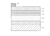
- the compound thin film solar cell includes a substrate 10. On the substrate 10, the back electrode 11, the light absorption layer 12, the buffer layer 13, the semi-insulating layer 14, the window layer 15, and the surface electrode 16 are positioned in this order.
- a glass plate, a metal plate, or a resin film such as plastic is used as the substrate 10.
- a metal such as Mo, Ni, Cu, Ti, Fe, Al, titania, stainless steel, or the like is used.
- a carbon-based electrode such as carbon or graphene, or a transparent conductive film such as ITO (Indium Tin Oxide) or ZnO may be used.
- the light absorption layer 12 is a p-type compound semiconductor.
- the light absorption layer 12 is composed of a CZTS-based compound semiconductor, that is, a CZTS semiconductor.
- the CZTS semiconductor comprises at least one element of group VIB (group 16) S and group VIB (group 16) Se, group IB (group 11) Cu, group IIB (group 12) Zn, and It is a compound semiconductor containing three elements of Sn of group IVB (group 14). That is, the CZTS semiconductor is a IB 2- (IIB-IVB) -VIB Group 4 compound semiconductor.
- the Cu / (Zn + Sn) ratio in the light absorption layer 12 and the Zn / Sn ratio in the light absorption layer 12 are The coordinates (x, y) indicating are in the following range. That is, the coordinates (x, y) indicated by the light absorption layer 12 are composed of seven line segments connecting the following coordinates A, coordinates B, coordinates C, coordinates D, coordinates E, coordinates F, coordinates G, and coordinates A in this order. It is located on the line or inside the area surrounded by these seven line segments.
- the seven line segments are a line segment connecting coordinates A and B, a line segment connecting coordinates B and C, a line segment connecting coordinates C and D, coordinates D and E, , A line segment connecting coordinates E and F, a line segment connecting coordinates F and G, and a line segment connecting coordinates G and A.
- ⁇ Coordinate A (0.71, 0.82) ⁇ Coordinate B (0.90, 0.82) ⁇ Coordinate C (0.94, 0.87) -Coordinate D (0.89, 1.00) ⁇ Coordinate E (0.84, 1.07) ⁇ Coordinate F (0.75, 1.08) ⁇ Coordinate G (0.71, 1.05)
- the Cu / (Zn + Sn) ratio and the Zn / Sn ratio are both atomic ratios.
- the Zn / Sn ratio in the portion close to the front electrode 16 is preferably lower than the Zn / Sn ratio in the portion close to the back electrode 11. According to such a configuration, the photoelectric conversion efficiency is further increased.
- the thickness of the light absorption layer 12 is preferably 0.3 ⁇ m or more and 10 ⁇ m or less, and preferably 2 ⁇ m, for example.
- the buffer layer 13 is an n-type compound semiconductor.
- the buffer layer 13 for example, CdS, Zn (S, O, OH), ZnS, ZnSe, In 2 S 3 or the like is used.
- the semi-insulating layer 14 is an i-type compound semiconductor.
- the window layer 15 is an n-type compound semiconductor. As the window layer 15, for example, ZnO or ITO to which Al, Ga, B or the like is added is used.
- the surface electrode 16 is laminated on a part of the upper surface of the window layer 15.
- a material of the surface electrode 16 for example, a metal such as Al or Ag is used.
- a carbon-based electrode such as carbon or graphene, or a transparent conductive film such as ITO or ZnO may be used.
- the compound thin film solar cell may have layers other than said each layer.
- an antireflection film may be laminated on the window layer 15. Since the antireflection film has a function of suppressing light reflection, the light absorption layer 12 can absorb more light by providing the antireflection film.
- the antireflection film is made of MgF 2 to a thickness of about 100 nm, for example.
- an intermediate layer having a composition for increasing the photoelectric conversion efficiency may be provided between the back electrode 11 and the light absorption layer 12.
- the compound thin film solar cell is formed by laminating a back electrode 11, a light absorption layer 12, a buffer layer 13, a semi-insulating layer 14, a window layer 15, and a surface electrode 16 in this order on a substrate 10.
- the back electrode 11 is formed on the upper surface of the substrate 10 by using, for example, sputtering, vapor deposition, CVD (Chemical Vapor Deposition), or the like.
- the light absorption layer 12 is formed using a light absorption layer forming ink containing fine particles composed of the constituent elements of the light absorption layer 12.
- the fine particles are nano-sized particles.
- the fine particles are generated by a reaction between a solution containing a metal salt or a metal complex and a solution containing a chalcogenide salt.
- the fine particles are, for example, particles made of a compound represented by a composition formula of Cu 2-x Zn 1 + y SnS z Se 4-Z (0 ⁇ x ⁇ 1, 0 ⁇ y ⁇ 1, 0 ⁇ z ⁇ 4).
- the ink for forming the light absorption layer is formed of Cu 2-x S y Se 2-y (0 ⁇ x ⁇ 1, 0 ⁇ y ⁇ 2), Zn 2-x as fine particles in addition to the particles composed of the above compound.
- the light absorption layer forming ink is represented by a composition formula of Cu 2 ⁇ x Zn 1 + y SnS z Se 4 ⁇ Z (0 ⁇ x ⁇ 1, 0 ⁇ y ⁇ 1, 0 ⁇ z ⁇ 4) as fine particles.
- the particles made of the compound the particles made of three kinds of compounds included in the group may be included.
- the coordinates (x, y) indicated by the light absorbing layer forming ink are coordinates derived from all fine particles contained in the light absorbing layer forming ink (x Y).
- the coordinate (x, y) which the ink for light absorption layer formation shows is the following ranges. That is, the coordinates (x, y) indicated by the light absorbing layer forming ink include seven lines connecting the following coordinates A, coordinates B, coordinates C, coordinates D, coordinates E, coordinates F, coordinates G, and coordinates A in this order. It is located on the line including the minute or inside the area surrounded by these seven line segments.
- the seven line segments are a line segment connecting coordinates A and B, a line segment connecting coordinates B and C, a line segment connecting coordinates C and D, coordinates D and E, , A line connecting the coordinates E and F, a line connecting the coordinates F and G, and a line connecting the coordinates G and A.
- the light absorbing layer 12 capable of increasing the photoelectric conversion efficiency can be formed.
- the coordinates (x, y) indicated by each fine particle may be included in the above range with respect to the composition ratio of each of the fine particles included in the light absorbing layer forming ink. Fine particles having coordinates (x, y) outside the above range may be included in the fine particles contained in the layer forming ink.
- amorphous particles As the fine particles, it is preferable to use amorphous particles. Since the energy of crystalline particles is in a stable state, each molecule contained in the particles is likely to be fixed at a certain position, that is, difficult to diffuse, but each component of amorphous particles diffuses by heat treatment. It's easy to do. Therefore, the use of amorphous particles improves the density of the light absorption layer 12.
- the average particle size of the fine particles is preferably 1 nm or more and 200 nm or less.
- the average particle size of the fine particles is determined by observing the nanoparticles with a SEM (scanning electron microscope).
- the average particle diameter of the fine particles is the shortest diameter of each fine particle included in five observation regions each having a 1 ⁇ m square area when a cured product of the light absorbing layer forming ink is observed using an SEM. Is the average value.
- the solvent for dispersing the fine particles in the light absorbing layer forming ink is not particularly limited as long as it is an organic solvent.
- the organic solvent can be selected from, for example, alcohols, ethers, esters, aliphatic hydrocarbons, alicyclic hydrocarbons, or aromatic hydrocarbons.
- alcohols having less than 10 carbon atoms such as methanol, ethanol, butanol, pyridine, diethyl ether, pentane, hexane, cyclohexane, and toluene are preferable, and methanol, pyridine, toluene, and hexane are particularly preferable.
- the light absorbing layer forming ink preferably contains a binder in order to improve leveling properties during coating.
- the content of the binder is preferably 5% by mass or more and 70% by mass or less, and more preferably 20% by mass or more and 60% by mass or less of the fine particles contained in the light absorbing layer forming ink.
- the binder content is 5% by mass or more, formation of cavities in the coating film after heat treatment is suppressed.
- the binder content is 70% by mass or less, an increase in the surface roughness of the coating film after the heat treatment is suppressed.
- a thiol organic substance, a selenol organic substance, or an alcohol having 10 or more carbon atoms can be used.
- Se particles, S particles, Se compounds, S compounds, or the like may be used as the binder.
- sodium sulfide, sodium selenide, potassium selenide, sodium selenate, thiosulfate, or the like may be used as the binder.
- it is preferable to use a thiol organic substance as the binder it is preferable to use a thiol organic substance as the binder, and it is more preferable to use thiourea.
- the light absorption layer 12 formed from the light absorption layer forming ink has a trace amount of about 0.3 atomic% to 0.5 atomic% with respect to the entire light absorption layer 12. Of carbon remains.
- the light absorption layer forming ink is applied to the upper surface of the back electrode 11 to form a film containing fine particles. And the solvent contained in a film
- the light absorption layer 12 includes at least one element of S and Se and three elements of Cu, Zn, and Sn as elements derived from the fine particles.
- Examples of the coating method of the light absorbing layer forming ink include a doctor blade method, a spin coating method, a slit coating method, a coating method such as a spray method, a gravure printing method, a screen printing method, a reverse offset printing method, Or printing methods, such as a relief printing method, are mentioned.
- the heat treatment is performed, for example, by annealing using a heating furnace or rapid thermal annealing (RTA).
- the atmosphere of the heat treatment is at least selected from the group consisting of H 2 S gas, H 2 Se gas, nitrogen gas, Ar gas, Se vapor, S vapor, hydrogen gas, and a mixed gas of hydrogen and an inert gas. Preferably one is included.
- the heat treatment temperature is preferably 250 ° C. or higher.
- the temperature of the heat treatment is a temperature that the glass can withstand, specifically, 650 ° C. or less is preferable, and 600 ° C. or less is more preferable.
- the heat treatment is preferably performed in the presence of an alkali metal such as sodium.
- a layer containing an alkali metal is formed on the upper surface of the back electrode 11, and a light absorbing layer forming ink is applied on the layer containing the alkali metal, and heat treatment is performed.
- a layer containing an alkali metal can be formed by depositing a NaNbO 3 compound, a KNbO 3 compound, or a LiNbO 3 compound on the upper surface of the back electrode 11 by sputtering.
- the layer containing an alkali metal can also be formed by depositing a compound such as Na 2 S, Na 2 Se, NaCl, or NaF on the upper surface of the back electrode 11 by vapor deposition or coating.
- the light absorbing layer 12 formed from the light absorbing layer forming ink is preferably treated with an acid such as hydrochloric acid.
- an acid such as hydrochloric acid.
- Zn atoms in the vicinity of the upper surface of the light absorption layer 12 are dissolved, so that the Zn / Sn ratio in the portion near the front electrode 16 in the light absorption layer 12 is higher than the Zn / Sn ratio in the portion near the back electrode 11.
- an acid a well-known inorganic acid and organic acid can be used.
- the buffer layer 13 is formed on the upper surface of the light absorption layer 12 by, for example, CBD (Chemical Bath Deposition) method, MOCVD (Metal Organic Chemical Vapor Deposition) method, or ALD (Atomic Layer Deposition) method.
- CBD Chemical Bath Deposition
- MOCVD Metal Organic Chemical Vapor Deposition
- ALD Atomic Layer Deposition
- the semi-insulating layer 14 is formed on the upper surface of the buffer layer 13 by using, for example, MOCVD or sputtering.
- the window layer 15 is formed on the upper surface of the semi-insulating layer 14 by using, for example, MOCVD or sputtering.
- the surface electrode 16 is formed on a part of the upper surface of the window layer 15 by using, for example, sputtering, vapor deposition, CVD, or the like.
- sputtering vapor deposition
- CVD chemical vapor deposition
- Example The compound thin film solar cell, the manufacturing method thereof, and the light absorption layer described above will be described using specific examples.
- a first solution was prepared by dissolving CuI (0.405 g), ZnI 2 (0.447 g), and SnI 4 (0.877 g) in 500 ml of pyridine.
- a second solution was prepared by dissolving Na 2 Se (0.658 g) in 125 ml of methanol.
- the coordinates (x, y) indicated by the light absorbing layer forming ink and the light absorbing layer are indicated.
- the coordinates (x, y) can be changed.
- the first solution and the second solution were mixed, and this mixed solution was reacted at 0 ° C. in an inert gas atmosphere to produce Cu—Zn—Sn—Se fine particles.
- the average particle diameter was 50 nm.
- the reaction solution is filtered and washed with methanol, and then the washed Cu—Zn—Sn—Se fine particles and thiourea are mixed so that the mass ratio of the fine particles to thiourea is 3: 2, and this mixture is mixed. Further, pyridine and methanol were further added to prepare a light absorbing layer forming ink containing Cu—Zn—Sn—Se fine particles.
- the solid content contained in the light absorbing layer forming ink is 2% by mass.
- a semi-insulating layer made of ZnO having a thickness of 50 nm was formed on the buffer layer by MOCVD using diethyl zinc and water as raw materials.
- a window layer made of ZnO: B having a thickness of 1 ⁇ m was formed on the semi-insulating layer by MOCVD using diethyl zinc, water, and diborane as raw materials.
- a surface electrode made of Al having a film thickness of 0.3 ⁇ m was formed on the window layer by vapor deposition. Thereby, a compound thin film solar cell was obtained.
- the Cu / (Zn + Sn) ratio of the light-absorbing layer after the heat treatment is adjusted by adjusting the amount of each of CuI, ZnI 2 , and SnI 4 when adjusting the light-absorbing layer forming ink.
- the compound thin film solar cells of Test Examples 1 to 22 having different Zn / Sn ratios were obtained.
- the compound thin film solar cell obtained when the added amount of CuI, ZnI 2 and SnI 4 is the above-described added amount corresponds to Test Example 20.
- composition ratio For the compound thin film solar cell of each test example, the cross section of the light absorption layer was flattened with Ar ions, and then Cu in atomic ratio was measured using TEM-EDS (energy dispersive X-ray analysis for transmission electron microscope). The / (Zn + Sn) ratio and the Zn / Sn ratio were evaluated.
- a two-dimensional orthogonal coordinate system in which the Cu / (Zn + Sn) ratio (atomic ratio) is on the x axis and the Zn / Sn ratio (atomic ratio) is on the y axis has coordinates A A region surrounded by a line segment connecting the coordinates G is formed.
- the coordinate A (0.71, 0.82) is Test Example 10
- the coordinate B (0.90, 0.82) is Test Example 22.
- the coordinates C (0.94, 0.87) is Test Example 12
- the coordinates D (0.89, 1.00) is Test Example 19.
- the coordinate E (0.84, 1.07) is Test Example 13
- the coordinate F (0.75, 1.08) is Test Example 14.
- Coordinate G (0.71, 1.05) is Test Example 15.
- the coordinates (x, y) indicated by the light absorption layer connect seven coordinates A to G in the order of coordinate A ⁇ coordinate B ⁇ coordinate C ⁇ coordinate D ⁇ coordinate E ⁇ coordinate F ⁇ coordinate G ⁇ coordinate A.
- a high photoelectric conversion efficiency of 4.0% or more was obtained.
- a light absorption layer formed by heat-treating a film formed by sputtering, and a coating film of ink containing fine particles as in the above embodiment is heat-treated.
- the progress of crystallization during the heat treatment is different from the formed light absorption layer.
- Such a difference in the progress of crystallization is considered to be a factor that greatly affects the photoelectric conversion efficiency. Therefore, the range of the composition ratio surrounded by the line segment connecting the coordinates A to G is a specific range in which the photoelectric conversion efficiency can be increased when the light absorption layer is formed by the manufacturing method using ink containing fine particles. This range is derived for the first time as a result of research focusing on differences in crystallization progress due to differences in production methods.
- the light absorption layer 12 contains carbon
- the light absorption layer forming ink containing the organic binder can be used for coating.
- the Cu / (Zn + Sn) ratio and the Zn / Sn ratio in the fine particle component in the light absorbing layer forming ink are included in the range surrounded by the line segment connecting the coordinates A to G, the photoelectric conversion efficiency is improved.
- the light absorption layer 12 having an enhanced composition can be formed.
- the fine particles contained in the light absorbing layer forming ink are amorphous particles, the denseness of the formed light absorbing layer 12 is improved.
- the average particle size of the fine particles contained in the light absorbing layer forming ink is 200 nm or less, formation of a gap in the film is suppressed in the heat treatment step when forming the light absorbing layer 12.
- the average particle diameter is 1 nm or more, the fine particles are less likely to aggregate, and thus the preparation of the light absorbing layer forming ink is facilitated.
- the ink for forming the light absorption layer contains a thiol organic substance
- the thiol organic substance functions as a binder, and the leveling property of the film during ink application is improved.
Landscapes
- Chemical & Material Sciences (AREA)
- Organic Chemistry (AREA)
- Life Sciences & Earth Sciences (AREA)
- Engineering & Computer Science (AREA)
- Materials Engineering (AREA)
- Wood Science & Technology (AREA)
- Inorganic Chemistry (AREA)
- Chemical Kinetics & Catalysis (AREA)
- General Chemical & Material Sciences (AREA)
- Photovoltaic Devices (AREA)
Abstract
Cu/(Zn+Sn)比(原子比)をx軸に、Zn/Sn比(原子比)をy軸に示す直交座標系において、化合物薄膜太陽電池が備える光吸収層のCu/(Zn+Sn)比とZn/Sn比とを示す座標(x、y)は、座標A(0.71、0.82)、座標B(0.90、0.82)、座標C(0.94、0.87)、座標D(0.89、1.00)、座標E(0.84、1.07)、座標F(0.75、1.08)、および、座標G(0.71、1.05)を座標A、座標B、座標C、座標D、座標E、座標F、座標G,座標Aの順に結ぶ、7つの線分からなる線の上、または、これら7つの線分で囲まれた領域の内部に位置する。
Description
本発明は、CZTS系の化合物半導体層を備える化合物薄膜太陽電池、その製造方法、および、上記化合物薄膜太陽電池に用いられる光吸収層に関する。
CZTS系化合物薄膜太陽電池は、CZTS系(Cu2ZnSnS4、Cu2ZnSnSe4、Cu2ZnSn(S,Se)4等)の化合物半導体層を光吸収層として備えている。こうした化合物薄膜太陽電池において、光吸収層の組成比は、光電変換効率に影響を与える因子の一つである。例えば、特許文献1には、Cu/(Zn+Sn)比が0.78~0.90であり、かつ、Zn/Sn比が1.18~1.32である光吸収層は、高い光電変換効率をもたらすことが開示されている。
しかしながら、特許文献1に開示されている組成比の範囲は、スパッタリングによって成膜された光吸収層を対象とした試験の結果から求められた範囲である。そのため、スパッタリングとは異なる方法によって成膜された光吸収層に、上記組成比を適用したとしても、必ずしも高い光電変換効率が得られるとは限らない。
例えば、微粒子を含むインクの塗膜から光吸収層を形成する方法は、スパッタリングと比較して、安価に光吸収層を形成することができる。そのため、こうした方法によって形成された光吸収層を備える化合物薄膜太陽電池の光電変換効率を高めることが求められている。
本発明は、微粒子を含むインクの塗膜から形成された光吸収層を備える化合物薄膜太陽電池において、光電変換効率を高めることのできる化合物薄膜太陽電池、化合物薄膜太陽電池の製造方法、および、光吸収層を提供することを目的とする。
上記課題を解決する化合物薄膜太陽電池は、化合物からなる微粒子を含むインクから形成された光吸収層を備える化合物薄膜太陽電池であって、前記光吸収層は、前記微粒子に由来する元素として、S、および、Seの少なくとも1つの元素と、Cu、Zn、および、Snの3つの元素とを含み、Cu/(Zn+Sn)比(原子比)をx軸に、Zn/Sn比(原子比)をy軸に示す直交座標系において、前記光吸収層の前記Cu/(Zn+Sn)比と前記Zn/Sn比とを示す座標(x、y)は、座標A(0.71、0.82)、座標B(0.90、0.82)、座標C(0.94、0.87)、座標D(0.89、1.00)、座標E(0.84、1.07)、座標F(0.75、1.08)、および、座標G(0.71、1.05)を座標A、座標B、座標C、座標D、座標E、座標F、座標G,座標Aの順に結ぶ、7つの線分からなる線の上、または、前記7つの線分で囲まれた領域の内部に位置する。
上記構成によれば、化合物薄膜太陽電池における光電変換効率が高められる。
上記課題を解決する化合物薄膜太陽電池の製造方法は、化合物からなる微粒子を含むインクを準備することと、前記インクの塗工によって塗膜を成膜することと、前記塗膜を熱処理して光吸収層を形成することと、を含み、前記インクを準備することは、以下の条件、a)前記インクが、前記微粒子に由来する元素として、S、および、Seの少なくとも1つの元素と、Cu、Zn、および、Snの3つの元素とを含み、かつ、b)Cu/(Zn+Sn)比(原子比)をx軸に、Zn/Sn比(原子比)をy軸に示す直交座標系において、前記光吸収層の前記Cu/(Zn+Sn)比と前記Zn/Sn比とを示す座標(x、y)が、座標A(0.71、0.82)、座標B(0.90、0.82)、座標C(0.94、0.87)、座標D(0.89、1.00)、座標E(0.84、1.07)、座標F(0.75、1.08)、および、座標G(0.71、1.05)を座標A、座標B、座標C、座標D、座標E、座標F、座標G,座標Aの順に結ぶ、7つの線分からなる線の上、または、前記7つの線分で囲まれた領域の内部に位置する、を満たすインクを準備することを含む。
上記課題を解決する化合物薄膜太陽電池の製造方法は、化合物からなる微粒子を含むインクを準備することと、前記インクの塗工によって塗膜を成膜することと、前記塗膜を熱処理して光吸収層を形成することと、を含み、前記インクを準備することは、以下の条件、a)前記インクが、前記微粒子に由来する元素として、S、および、Seの少なくとも1つの元素と、Cu、Zn、および、Snの3つの元素とを含み、かつ、b)Cu/(Zn+Sn)比(原子比)をx軸に、Zn/Sn比(原子比)をy軸に示す直交座標系において、前記光吸収層の前記Cu/(Zn+Sn)比と前記Zn/Sn比とを示す座標(x、y)が、座標A(0.71、0.82)、座標B(0.90、0.82)、座標C(0.94、0.87)、座標D(0.89、1.00)、座標E(0.84、1.07)、座標F(0.75、1.08)、および、座標G(0.71、1.05)を座標A、座標B、座標C、座標D、座標E、座標F、座標G,座標Aの順に結ぶ、7つの線分からなる線の上、または、前記7つの線分で囲まれた領域の内部に位置する、を満たすインクを準備することを含む。
上記製造方法によれば、光電変換効率の高められた化合物薄膜太陽電池を製造することができる。
上記課題を解決する光吸収層は、化合物からなる微粒子を含むインクから形成された光吸収層であって、前記光吸収層は、前記微粒子に由来する元素として、S、および、Seの少なくとも1つの元素と、Cu、Zn、および、Snの3つの元素とを含み、Cu/(Zn+Sn)比(原子比)をx軸に、Zn/Sn比(原子比)をy軸に示す直交座標系において、前記光吸収層の前記Cu/(Zn+Sn)比と前記Zn/Sn比とを示す座標(x、y)は、座標A(0.71、0.82)、座標B(0.90、0.82)、座標C(0.94、0.87)、座標D(0.89、1.00)、座標E(0.84、1.07)、座標F(0.75、1.08)、および、座標G(0.71、1.05)を座標A、座標B、座標C、座標D、座標E、座標F、座標G,座標Aの順に結ぶ、7つの線分からなる線の上、または、前記7つの線分で囲まれた領域の内部に位置する。
上記課題を解決する光吸収層は、化合物からなる微粒子を含むインクから形成された光吸収層であって、前記光吸収層は、前記微粒子に由来する元素として、S、および、Seの少なくとも1つの元素と、Cu、Zn、および、Snの3つの元素とを含み、Cu/(Zn+Sn)比(原子比)をx軸に、Zn/Sn比(原子比)をy軸に示す直交座標系において、前記光吸収層の前記Cu/(Zn+Sn)比と前記Zn/Sn比とを示す座標(x、y)は、座標A(0.71、0.82)、座標B(0.90、0.82)、座標C(0.94、0.87)、座標D(0.89、1.00)、座標E(0.84、1.07)、座標F(0.75、1.08)、および、座標G(0.71、1.05)を座標A、座標B、座標C、座標D、座標E、座標F、座標G,座標Aの順に結ぶ、7つの線分からなる線の上、または、前記7つの線分で囲まれた領域の内部に位置する。
上記構成によれば、化合物薄膜太陽電池における光電変換効率が高められる。
図1を参照して、化合物薄膜太陽電池、その製造方法、および、光吸収層の一実施形態について説明する。
[化合物薄膜太陽電池の構成]
図1に示されるように、化合物薄膜太陽電池は、基板10を備える。基板10の上には、裏面電極11、光吸収層12、バッファ層13、半絶縁層14、窓層15、および、表面電極16がこの順に位置している。
[化合物薄膜太陽電池の構成]
図1に示されるように、化合物薄膜太陽電池は、基板10を備える。基板10の上には、裏面電極11、光吸収層12、バッファ層13、半絶縁層14、窓層15、および、表面電極16がこの順に位置している。
基板10としては、例えば、ガラス板、金属板、または、プラスチック等の樹脂フィルムが用いられる。
裏面電極11の材料としては、例えば、Mo、Ni、Cu、Ti、Fe、Al、チタニア、ステンレス等の金属が用いられる。あるいは、裏面電極11として、カーボンやグラフェン等のカーボン系電極、または、ITO(Indium Tin Oxide)やZnO等の透明導電膜が用いられてもよい。
裏面電極11の材料としては、例えば、Mo、Ni、Cu、Ti、Fe、Al、チタニア、ステンレス等の金属が用いられる。あるいは、裏面電極11として、カーボンやグラフェン等のカーボン系電極、または、ITO(Indium Tin Oxide)やZnO等の透明導電膜が用いられてもよい。
光吸収層12は、p型化合物半導体である。光吸収層12は、CZTS系の化合物半導体、すなわちCZTS半導体から構成される。CZTS半導体は、VIB族(16族)のS、および、VIB族(16族)のSeの少なくとも1つの元素と、IB族(11族)のCu、IIB族(12族)のZn、および、IVB族(14族)のSnの3つの元素とを含む化合物半導体である。すなわち、CZTS半導体は、IB2-(IIB-IVB)-VIB4族の化合物半導体である。
Cu/(Zn+Sn)比をx軸に、Zn/Sn比をy軸に示す二次元の直交座標系において、光吸収層12におけるCu/(Zn+Sn)比と光吸収層12におけるZn/Sn比とを示す座標(x,y)は、以下の範囲である。すなわち、光吸収層12の示す座標(x,y)は、下記座標A、座標B、座標C、座標D、座標E、座標F、座標G、座標Aをこの順に結ぶ、7つの線分からなる線の上、または、それら7つの線分によって囲まれた領域の内部に位置する。なお、7つの線分は、座標Aと座標Bとを結ぶ線分と、座標Bと座標Cとを結ぶ線分と、座標Cと座標Dとを結ぶ線分と、座標Dと座標Eとを結ぶ線分と、座標Eと座標Fとを結ぶ線分と、座標Fと座標Gとを結ぶ線分と、座標Gと座標Aとを結ぶ線分とを含む。
・座標A(0.71、0.82)
・座標B(0.90、0.82)
・座標C(0.94、0.87)
・座標D(0.89、1.00)
・座標E(0.84、1.07)
・座標F(0.75、1.08)
・座標G(0.71、1.05)
なお、上記のCu/(Zn+Sn)比、および、Zn/Sn比は、ともに原子比である。光吸収層12の示す座標(x,y)が上記の範囲内であれば、化合物薄膜太陽電池の光電変換効率が高められる。
光吸収層12において、表面電極16に近い部分のZn/Sn比は、裏面電極11に近い部分のZn/Sn比よりも低いことが好ましい。こうした構成によれば、光電変換効率がさらに高められる。光吸収層12の厚さは、0.3μm以上10μm以下であることが好ましく、例えば、2μmであることが好ましい。
バッファ層13は、n型化合物半導体である。バッファ層13としては、例えば、CdS、Zn(S,O,OH)、ZnS、ZnSe、または、In2S3等が用いられる。半絶縁層14は、i型化合物半導体である。半絶縁層14としては、例えば、ZnO等の金属酸化物が用いられる。窓層15は、n型化合物半導体である。窓層15としては、例えば、Al、Ga、または、B等が添加されたZnOやITOが用いられる。
表面電極16は、窓層15の上面の一部に積層されている。表面電極16の材料としては、例えば、Al、Ag等の金属が用いられる。あるいは、表面電極16として、カーボンやグラフェン等のカーボン系電極、または、ITOやZnO等の透明導電膜が用いられてもよい。
なお、バッファ層13、半絶縁層14、および、窓層15の少なくとも1つが省略されてもよい。また、化合物薄膜太陽電池は、上記各層以外の他の層を有していてもよい。例えば、窓層15の上に、反射防止膜が積層されていてもよい。反射防止膜は光の反射を抑える機能を有するため、反射防止膜を設けることによって、光吸収層12はより多くの光を吸収することができる。反射防止膜は、例えば、100nm程度の厚さに、MgF2から形成される。
また例えば、裏面電極11と光吸収層12との間に、光電変換効率を高めるための組成を有する中間層が設けられていてもよい。
[化合物薄膜太陽電池の製造方法]
化合物薄膜太陽電池は、基板10の上に、裏面電極11、光吸収層12、バッファ層13、半絶縁層14、窓層15、表面電極16が、この順に積層されることによって形成される。
[化合物薄膜太陽電池の製造方法]
化合物薄膜太陽電池は、基板10の上に、裏面電極11、光吸収層12、バッファ層13、半絶縁層14、窓層15、表面電極16が、この順に積層されることによって形成される。
裏面電極11は、基板10の上面に、例えば、スパッタリング、蒸着法、CVD(Chemical Vapor Deposition)法等を用いて形成される。
光吸収層12は、光吸収層12の構成元素から構成される微粒子を含む光吸収層形成用インクを用いて形成される。
光吸収層12は、光吸収層12の構成元素から構成される微粒子を含む光吸収層形成用インクを用いて形成される。
微粒子は、ナノサイズの粒子である。微粒子は、金属塩または金属錯体を含む溶液と、カルコゲニド塩を含む溶液との反応によって生成される。微粒子は、例えば、Cu2-xZn1+ySnSzSe4-Z(0≦x≦1、0≦y≦1、0≦z≦4)の組成式で表される化合物からなる粒子である。また、光吸収層形成用インクは、微粒子として、上記化合物からなる粒子に加えて、Cu2-xSySe2-y(0≦x≦1、0≦y≦2)、Zn2-xSySe2-y(0≦x≦1、0≦y≦2)、Sn2-xSySe2-y(0≦x≦1、0≦y≦2)の組成式で表される化合物からなる群から選択される少なくとも1種以上の化合物からなる粒子を含んでいてもよい。あるいは、光吸収層形成用インクは、微粒子として、Cu2-xZn1+ySnSzSe4-Z(0≦x≦1、0≦y≦1、0≦z≦4)の組成式で表される化合物からなる粒子に代えて、上記群に含まれる3種類の化合物からなる粒子を含んでいてもよい。
上記直交座標系において、光吸収層形成用インクの組成比について、光吸収層形成用インクの示す座標(x,y)は、光吸収層形成用インクに含まれる全微粒子に由来する座標(x、y)である。そして、光吸収層形成用インクの示す座標(x,y)は、以下の範囲である。すなわち、光吸収層形成用インクの示す座標(x,y)は、下記座標A、座標B、座標C、座標D、座標E、座標F、座標G、座標Aをこの順に結ぶ、7つの線分を含む線の上、または、それら7つの線分によって囲まれた領域の内部に位置する。なお、7つの線分は、座標Aと座標Bとを結ぶ線分と、座標Bと座標Cとを結ぶ線分と、座標Cと座標Dとを結ぶ線分と、座標Dと座標Eとを結ぶ線分と、座標Eと座標Fとを結ぶ線分と、座標Fと座標Gとを結ぶ線分と、座標Gと座標Aを結ぶ線分とを含む。
・座標A(0.71、0.82)
・座標B(0.90、0.82)
・座標C(0.94、0.87)
・座標D(0.89、1.00)
・座標E(0.84、1.07)
・座標F(0.75、1.08)
・座標G(0.71、1.05)
光吸収層形成用インクの示す座標(x,y)が上記の範囲内であれば、光電変換効率を高めることのできる光吸収層12を形成することができる。なお、光吸収層形成用インクでは、光吸収層形成用インクに含まれる微粒子の各々の組成比について、各微粒子の示す座標(x,y)が上記範囲に含まれてもよいし、光吸収層形成用インクに含まれる微粒子の中に上記範囲外の座標(x,y)を示す微粒子が含まれてもよい。
・座標A(0.71、0.82)
・座標B(0.90、0.82)
・座標C(0.94、0.87)
・座標D(0.89、1.00)
・座標E(0.84、1.07)
・座標F(0.75、1.08)
・座標G(0.71、1.05)
光吸収層形成用インクの示す座標(x,y)が上記の範囲内であれば、光電変換効率を高めることのできる光吸収層12を形成することができる。なお、光吸収層形成用インクでは、光吸収層形成用インクに含まれる微粒子の各々の組成比について、各微粒子の示す座標(x,y)が上記範囲に含まれてもよいし、光吸収層形成用インクに含まれる微粒子の中に上記範囲外の座標(x,y)を示す微粒子が含まれてもよい。
微粒子としては、非晶質の粒子を用いることが好ましい。結晶性の粒子のエネルギーは安定な状態にあるため、粒子に含まれる各分子が一定の位置に固定されやすい、すなわち、拡散しにくいが、非晶質の粒子の各組成成分は、熱処理によって拡散しやすい。そのため、非晶質の粒子が用いられることによって、光吸収層12の緻密性が向上する。
微粒子の平均粒径は、1nm以上200nm以下であることが好ましい。平均粒径が200nm以下であると、光吸収層12を形成する際の熱処理工程において、膜に隙間が形成されることが抑えられる。そのため、光吸収層12における表面粗さの増加や、光電変換効率の低下が抑えられる。一方、微粒子の平均粒径が1nm以上であると、微粒子が凝集しにくくなるため、光吸収層形成用インクの調製が容易となる。なお、微粒子の平均粒径は、SEM(走査型電子顕微鏡)によるナノ粒子の観察によって求められる。具体的には、微粒子の平均粒径は、光吸収層形成用インクの硬化物をSEMを用いて観察した場合における、1μm四方の領域を有する5個の観測領域に含まれる各微粒子の最短径の平均値である。
光吸収層形成用インクにて微粒子を分散させる溶媒は、有機溶媒であれば、特に制限されない。有機溶媒は、例えば、アルコール、エーテル、エステル、脂肪族炭化水素、脂環族炭化水素、または、芳香族炭化水素等から選択することができる。有機溶媒としては、メタノール、エタノール、ブタノール等の炭素数10未満のアルコール、ピリジン、ジエチールエーテル、ペンタン、ヘキサン、シクロヘキサン、および、トルエンが好ましく、メタノール、ピリジン、トルエン、および、ヘキサンが特に好ましい。
光吸収層形成用インクは、塗工時のレベリング性を高めるために、バインダを含むことが好ましい。バインダの含有量は、光吸収層形成用インクが含む微粒子の5質量%以上70質量%以下であることが好ましく、20質量%以上60質量%以下であることがさらに好ましい。バインダの含有量が5質量%以上であることによって、熱処理後の塗膜に空洞が形成されることが抑えられる。バインダの含有量が70質量%以下であることによって、熱処理後の塗膜の表面粗さが大きくなることが抑えられる。
バインダとしては、チオール有機物、セレノール有機物、または、炭素数10以上のアルコール類等を用いることができる。また、バインダとして、Se粒子、S粒子、Se化合物、あるいは、S化合物等が用いられてもよい。さらには、バインダとして、硫化ナトリウム、セレン化ナトリウム、セレン化カリウム、セレン酸ナトリウム、あるいは、チオ硫酸塩等が用いられてもよい。これらの物質の中で、バインダとしては、チオール有機物を用いることが好ましく、チオ尿素を用いることがさらに好ましい。バインダとして有機化合物が用いられた場合、光吸収層形成用インクから形成された光吸収層12には、光吸収層12の全体に対して0.3原子%~0.5原子%程度の微量の炭素が残留する。
光吸収層12の形成工程では、まず、光吸収層形成用インクが、裏面電極11の上面に塗工されて、微粒子を含む膜が形成される。そして、塗工された膜が乾燥されることによって、膜に含まれる溶媒が除去され、光吸収層12の前駆体である塗膜が形成される。塗膜が熱処理されることによって、微粒子同士の焼結と結晶化とが進行して、光吸収層12が形成される。光吸収層12は、微粒子に由来する元素として、S、および、Seの少なくとも1つの元素と、Cu、Zn、および、Snの3つの元素とを含む。
光吸収層形成用インクの塗工方法としては、例えば、ドクターブレード法、スピンコーティング法、スリットコーティング法、または、スプレー法等の塗布法や、グラビア印刷法、スクリーン印刷法、反転オフセット印刷法、または、凸版印刷法等の印刷法が挙げられる。
熱処理は、例えば、加熱炉を用いたアニール処理や、ラピッドサーマルアニール(RTA)によって行われる。熱処理の雰囲気は、H2Sガス、H2Seガス、窒素ガス、Arガス、Se蒸気、S蒸気、水素ガス、および、水素と不活性ガスの混合ガスから構成される群から選択される少なくとも1つを含むことが好ましい。熱処理の温度は250℃以上が好ましい。基板10としてガラスが用いられる場合には、熱処理の温度は、ガラスが耐え得る温度、具体的には、650℃以下が好ましく、600℃以下がより好ましい。
なお、上記の熱処理は、ナトリウム等のアルカリ金属の共存下で行われることが好ましい。例えば、裏面電極11の上面に、アルカリ金属を含む層が形成され、アルカリ金属を含む層の上に光吸収層形成用インクが塗工されて、熱処理が行われる。具体的には、例えば、NaNbO3化合物、KNbO3化合物、あるいは、LiNbO3化合物が、スパッタリングによって裏面電極11の上面に堆積されることにより、アルカリ金属を含む層を作ることができる。また、アルカリ金属を含む層は、Na2S、Na2Se、NaCl、あるいは、NaF等の化合物が、蒸着や塗布によって裏面電極11の上面に堆積されることにより、形成することもできる。
光吸収層形成用インクから形成された光吸収層12には、塩酸等の酸による処理が施されることが好ましい。これによって、光吸収層12の上面付近のZn原子が溶け出すため、光吸収層12の中で表面電極16に近い部分のZn/Sn比を、裏面電極11に近い部分のZn/Sn比よりも積極的に低くすることができる。なお、酸としては、公知の無機酸や有機酸を用いることができる。
バッファ層13は、光吸収層12の上面に、例えば、CBD(Chemical Bath Deposition)法、MOCVD(Metal Organic Chemical Vapor Deposition)法、または、ALD(Atomic Layer Deposition)法等を用いて形成される。
半絶縁層14は、バッファ層13の上面に、例えば、MOCVD法やスパッタリングを用いて形成される。窓層15は、半絶縁層14の上面に、例えば、MOCVD法やスパッタリングを用いて形成される。
表面電極16は、窓層15の上面の一部に、例えば、スパッタリング、蒸着法、CVD法等を用いて形成される。
(実施例)
上述した化合物薄膜太陽電池、その製造方法、および、光吸収層について、具体的な実施例を用いて説明する。
(実施例)
上述した化合物薄膜太陽電池、その製造方法、および、光吸収層について、具体的な実施例を用いて説明する。
<化合物薄膜太陽電池の作製>
(光吸収層形成用インクの調整)
CuI(0.405g)、ZnI2(0.447g)、および、SnI4(0.877g)を500mlのピリジンに溶解して、第1の溶液を調製した。また、Na2Se(0.658g)を125mlのメタノールに溶解して、第2の溶液を調製した。この際、第1の溶液へのCuI、ZnI2、SnI4の各々の添加量を調整することによって、光吸収層形成用インクの示す上記座標(x,y)、および、光吸収層の示す上記座標(x,y)を変更することができる。
(光吸収層形成用インクの調整)
CuI(0.405g)、ZnI2(0.447g)、および、SnI4(0.877g)を500mlのピリジンに溶解して、第1の溶液を調製した。また、Na2Se(0.658g)を125mlのメタノールに溶解して、第2の溶液を調製した。この際、第1の溶液へのCuI、ZnI2、SnI4の各々の添加量を調整することによって、光吸収層形成用インクの示す上記座標(x,y)、および、光吸収層の示す上記座標(x,y)を変更することができる。
第1の溶液と第2の溶液とを混合し、この混合液を不活性ガス雰囲気下、0℃で反応させてCu-Zn-Sn-Se微粒子を製造した。こうして得られた微粒子の平均粒径をSEM(走査型電子顕微鏡)を用いて測定した結果、平均粒径は50nmであった。反応溶液を濾過してメタノールで洗浄した後、洗浄後のCu-Zn-Sn-Se微粒子とチオ尿素とを、微粒子とチオ尿素との質量比が3:2となるように混合し、この混合物にピリジンとメタノールとをさらに加えて、Cu-Zn-Sn-Se微粒子を含む光吸収層形成用インクを調整した。光吸収層形成用インクに含まれる固形分は2質量%である。
(裏面電極の形成)
基板としてソーダライムガラスを用い、スパッタリングによってMoから構成される裏面電極を形成した。
基板としてソーダライムガラスを用い、スパッタリングによってMoから構成される裏面電極を形成した。
(光吸収層の形成)
裏面電極の上面にスプレー法によって光吸収層形成用インクを塗布し、250℃のオーブンで溶媒を蒸発させて塗膜を形成した後に、上記塗膜を有する裏面電極をSe粉末と一緒に熱処理炉に入れて、550℃で60分、Se雰囲気の条件で熱処理を行った。これにより、膜厚が2μmのCZTS薄膜から構成される光吸収層が得られた。
裏面電極の上面にスプレー法によって光吸収層形成用インクを塗布し、250℃のオーブンで溶媒を蒸発させて塗膜を形成した後に、上記塗膜を有する裏面電極をSe粉末と一緒に熱処理炉に入れて、550℃で60分、Se雰囲気の条件で熱処理を行った。これにより、膜厚が2μmのCZTS薄膜から構成される光吸収層が得られた。
(バッファ層の形成)
0.0015Mの硫酸カドミウム(CdSO4)、0.0075Mのチオ尿素(NH2CSNH2)、および、1.5Mのアンモニア水(NH4OH)を含有する混合液を67℃に加熱した。この混合液中に、上述の光吸収層が形成された構造体を浸漬することによって、光吸収層上に膜厚が100nmのCdSから構成されるバッファ層が形成された。
0.0015Mの硫酸カドミウム(CdSO4)、0.0075Mのチオ尿素(NH2CSNH2)、および、1.5Mのアンモニア水(NH4OH)を含有する混合液を67℃に加熱した。この混合液中に、上述の光吸収層が形成された構造体を浸漬することによって、光吸収層上に膜厚が100nmのCdSから構成されるバッファ層が形成された。
(半絶縁層の形成)
ジエチル亜鉛と水とを原料としたMOCVD法によって、膜厚が50nmのZnOから構成される半絶縁層をバッファ層の上に形成した。
ジエチル亜鉛と水とを原料としたMOCVD法によって、膜厚が50nmのZnOから構成される半絶縁層をバッファ層の上に形成した。
(窓層の形成)
ジエチル亜鉛、水、および、ジボランを原料としたMOCVD法によって、膜厚が1μmのZnO:Bから構成される窓層を半絶縁層の上に形成した。
ジエチル亜鉛、水、および、ジボランを原料としたMOCVD法によって、膜厚が1μmのZnO:Bから構成される窓層を半絶縁層の上に形成した。
(表面電極の形成)
蒸着法を用いて、膜厚が0.3μmのAlから構成される表面電極を窓層の上に形成した。これによって、化合物薄膜太陽電池が得られた。
蒸着法を用いて、膜厚が0.3μmのAlから構成される表面電極を窓層の上に形成した。これによって、化合物薄膜太陽電池が得られた。
上記の方法において、光吸収層形成用インクの調整の際、CuI、ZnI2、SnI4の各々の添加量を調整することによって、上記の熱処理後の光吸収層のCu/(Zn+Sn)比およびZn/Sn比が互いに異なる試験例1~22の化合物薄膜太陽電池を得た。なお、CuI、ZnI2、SnI4の添加量が上記の添加量である場合に得られた化合物薄膜太陽電池は、試験例20に相当する。
<評価方法>
(光電変換効率)
各試験例の化合物薄膜太陽電池について、標準太陽光シミュレータ(光強度:100mW/cm2、エアマス:1.5)を用いて、光電変換効率を評価した。
(光電変換効率)
各試験例の化合物薄膜太陽電池について、標準太陽光シミュレータ(光強度:100mW/cm2、エアマス:1.5)を用いて、光電変換効率を評価した。
(組成比)
各試験例の化合物薄膜太陽電池について、Arイオンで光吸収層の断面を平らに研磨した後に、TEM-EDS(透過型電子顕微鏡用エネルギー分散型X線分析)を用いて、原子比でのCu/(Zn+Sn)比およびZn/Sn比を評価した。
各試験例の化合物薄膜太陽電池について、Arイオンで光吸収層の断面を平らに研磨した後に、TEM-EDS(透過型電子顕微鏡用エネルギー分散型X線分析)を用いて、原子比でのCu/(Zn+Sn)比およびZn/Sn比を評価した。
<結果>
各試験例の化合物薄膜太陽電池について、組成比および光電変換効率の評価結果を表1および図2に示す。
各試験例の化合物薄膜太陽電池について、組成比および光電変換効率の評価結果を表1および図2に示す。

なお、上述のように微粒子を含むインクの塗膜から形成された光吸収層に、特許文献1に開示されている組成比を適用した場合、光吸収層にZnSが大量に偏析し、光電変換効率は低かった。例えば、特許文献1に開示されている組成比の範囲に含まれる試験例2や、試験例2に近い組成比を有する試験例1や試験例3では、光電変換効率は極めて低い。試験例1~22の評価結果によれば、特にZn/Sn比が、特許文献1に開示されている組成比よりも低い範囲にあるとき、高い光電変換効率が得られることが認められた。特許文献1に記載のように、スパッタリングによって成膜された膜が熱処理されることによって形成される光吸収層と、上記実施形態のように、微粒子を含むインクの塗膜が熱処理されることによって形成される光吸収層とは、熱処理時における結晶化の進み方が異なる。こうした結晶化の進行の違いは、光電変換効率に大きな影響を与える要因であると考えられる。したがって、座標A~座標Gを結ぶ線分によって囲まれる組成比の範囲は、微粒子を含むインクを用いた製法によって光吸収層を形成した場合に光電変換効率の高められる特有の範囲であって、この範囲は、製法の違いに起因した結晶化の進行の差異に着目した研究の結果、はじめて導き出される。
以上、実施例を用いて説明したように、上記実施形態によれば、以下に列挙する効果を得ることができる。
(1)熱処理後の光吸収層12のCu/(Zn+Sn)比とZn/Sn比とが、上記座標A~座標Gを結ぶ線分によって囲まれる範囲に含まれると、化合物薄膜太陽電池における光電変換効率が高められる。
(1)熱処理後の光吸収層12のCu/(Zn+Sn)比とZn/Sn比とが、上記座標A~座標Gを結ぶ線分によって囲まれる範囲に含まれると、化合物薄膜太陽電池における光電変換効率が高められる。
(2)光吸収層12の中で、表面電極16に近い部分のZn/Sn比が、裏面電極11に近い部分のZn/Sn比よりも低いと、化合物薄膜太陽電池における光電変換効率がさらに高められる。
(3)光吸収層12が炭素を含むと、有機バインダが含まれた光吸収層形成用インクを塗工に使用できる。
(4)光吸収層形成用インク中の微粒子成分におけるCu/(Zn+Sn)比とZn/Sn比とが、座標A~座標Gを結ぶ線分によって囲まれる範囲に含まれると、光電変換効率の高められる組成を有する光吸収層12を形成することができる。
(4)光吸収層形成用インク中の微粒子成分におけるCu/(Zn+Sn)比とZn/Sn比とが、座標A~座標Gを結ぶ線分によって囲まれる範囲に含まれると、光電変換効率の高められる組成を有する光吸収層12を形成することができる。
(5)光吸収層形成用インクに含まれる微粒子が、非晶質の粒子であると、形成される光吸収層12の緻密性が向上する。
(6)光吸収層形成用インクに含まれる微粒子の平均粒径が200nm以下であると、光吸収層12を形成する際の熱処理工程において、膜に隙間が形成されることが抑えられる。一方、平均粒径が1nm以上であると、微粒子が凝集しにくくなるため、光吸収層形成用インクの調製が容易となる。
(6)光吸収層形成用インクに含まれる微粒子の平均粒径が200nm以下であると、光吸収層12を形成する際の熱処理工程において、膜に隙間が形成されることが抑えられる。一方、平均粒径が1nm以上であると、微粒子が凝集しにくくなるため、光吸収層形成用インクの調製が容易となる。
(7)光吸収層形成用インクがチオール有機物を含むと、チオール有機物がバインダとして機能し、インクの塗工時における膜のレベリング性が向上する。
Claims (8)
- 化合物からなる微粒子を含むインクから形成された光吸収層を備える化合物薄膜太陽電池であって、
前記光吸収層は、前記微粒子に由来する元素として、S、および、Seの少なくとも1つの元素と、Cu、Zn、および、Snの3つの元素とを含み、
Cu/(Zn+Sn)比(原子比)をx軸に、Zn/Sn比(原子比)をy軸に示す直交座標系において、前記光吸収層の前記Cu/(Zn+Sn)比と前記Zn/Sn比とを示す座標(x、y)は、座標A(0.71、0.82)、座標B(0.90、0.82)、座標C(0.94、0.87)、座標D(0.89、1.00)、座標E(0.84、1.07)、座標F(0.75、1.08)、および、座標G(0.71、1.05)を座標A、座標B、座標C、座標D、座標E、座標F、座標G,座標Aの順に結ぶ、7つの線分からなる線の上、または、前記7つの線分で囲まれた領域の内部に位置する
化合物薄膜太陽電池。 - 表面電極と裏面電極とをさらに備え、
前記光吸収層は、前記表面電極と前記裏面電極との間に位置し、
前記光吸収層の中で、前記表面電極に近い部分の前記Zn/Sn比は、前記裏面電極に近い部分の前記Zn/Sn比よりも低い
請求項1に記載の化合物薄膜太陽電池。 - 前記光吸収層は炭素を含む
請求項1または2に記載の化合物薄膜太陽電池。 - 化合物薄膜太陽電池の製造方法であって、
化合物からなる微粒子を含むインクを準備することと、
前記インクの塗工によって塗膜を成膜することと、
前記塗膜を熱処理して光吸収層を形成することと、
を含み、
前記インクを準備することは、以下の条件
a)前記インクが、前記微粒子に由来する元素として、S、および、Seの少なくとも1つの元素と、Cu、Zn、および、Snの3つの元素とを含み、かつ
b)Cu/(Zn+Sn)比(原子比)をx軸に、Zn/Sn比(原子比)をy軸に示す直交座標系において、前記光吸収層の前記Cu/(Zn+Sn)比と前記Zn/Sn比とを示す座標(x、y)が、座標A(0.71、0.82)、座標B(0.90、0.82)、座標C(0.94、0.87)、座標D(0.89、1.00)、座標E(0.84、1.07)、座標F(0.75、1.08)、および、座標G(0.71、1.05)を座標A、座標B、座標C、座標D、座標E、座標F、座標G,座標Aの順に結ぶ、7つの線分からなる線の上、または、前記7つの線分で囲まれた領域の内部に位置する
を満たすインクを準備することを含む
化合物薄膜太陽電池の製造方法。 - 前記微粒子は非晶質の粒子である
請求項4に記載の化合物薄膜太陽電池の製造方法。 - 前記微粒子の平均粒径は1nm以上200nm以下である
請求項4または5に記載の化合物薄膜太陽電池の製造方法。 - 前記インクはチオール有機物を含む
請求項4~6のいずれか一項に記載の化合物薄膜太陽電池の製造方法。 - 化合物からなる微粒子を含むインクから形成された光吸収層であって、
前記光吸収層は、前記微粒子に由来する元素として、S、および、Seの少なくとも1つの元素と、Cu、Zn、および、Snの3つの元素とを含み、
Cu/(Zn+Sn)比(原子比)をx軸に、Zn/Sn比(原子比)をy軸に示す直交座標系において、前記光吸収層の前記Cu/(Zn+Sn)比と前記Zn/Sn比とを示す座標(x、y)は、座標A(0.71、0.82)、座標B(0.90、0.82)、座標C(0.94、0.87)、座標D(0.89、1.00)、座標E(0.84、1.07)、座標F(0.75、1.08)、および、座標G(0.71、1.05)を座標A、座標B、座標C、座標D、座標E、座標F、座標G,座標Aの順に結ぶ、7つの線分からなる線の上、または、前記7つの線分で囲まれた領域の内部に位置する
光吸収層。
Applications Claiming Priority (2)
| Application Number | Priority Date | Filing Date | Title |
|---|---|---|---|
| JP2014-074195 | 2014-03-31 | ||
| JP2014074195A JP2015198126A (ja) | 2014-03-31 | 2014-03-31 | 化合物薄膜太陽電池、および、化合物薄膜太陽電池の製造方法 |
Publications (1)
| Publication Number | Publication Date |
|---|---|
| WO2015152257A1 true WO2015152257A1 (ja) | 2015-10-08 |
Family
ID=54240576
Family Applications (1)
| Application Number | Title | Priority Date | Filing Date |
|---|---|---|---|
| PCT/JP2015/060159 Ceased WO2015152257A1 (ja) | 2014-03-31 | 2015-03-31 | 化合物薄膜太陽電池、化合物薄膜太陽電池の製造方法、および、光吸収層 |
Country Status (3)
| Country | Link |
|---|---|
| JP (1) | JP2015198126A (ja) |
| TW (1) | TW201601332A (ja) |
| WO (1) | WO2015152257A1 (ja) |
Families Citing this family (1)
| Publication number | Priority date | Publication date | Assignee | Title |
|---|---|---|---|---|
| CN115108581B (zh) * | 2022-07-05 | 2024-03-15 | 许昌学院 | 一种常温制备铜锌锡硫纳米晶的化学方法 |
Citations (6)
| Publication number | Priority date | Publication date | Assignee | Title |
|---|---|---|---|---|
| WO2010095608A1 (ja) * | 2009-02-20 | 2010-08-26 | 株式会社豊田中央研究所 | 硫化物及び光電素子 |
| WO2012066116A1 (en) * | 2010-11-18 | 2012-05-24 | Université Du Luxembourg | Method of production of semiconductor thin films |
| JP2013070031A (ja) * | 2011-09-23 | 2013-04-18 | Delsolar Co Ltd | Czts吸収層を含む光電池装置及びその製造方法 |
| WO2013180137A1 (ja) * | 2012-05-30 | 2013-12-05 | 凸版印刷株式会社 | 化合物半導体薄膜の作製方法およびその化合物半導体薄膜を備える太陽電池 |
| JP2013544938A (ja) * | 2010-11-22 | 2013-12-19 | イー・アイ・デュポン・ドウ・ヌムール・アンド・カンパニー | 半導体インク、膜、コーティングされた基板および製造方法 |
| JP2014017426A (ja) * | 2012-07-11 | 2014-01-30 | Promatic Kk | 光電変換装置およびその製造方法 |
-
2014
- 2014-03-31 JP JP2014074195A patent/JP2015198126A/ja active Pending
-
2015
- 2015-03-31 WO PCT/JP2015/060159 patent/WO2015152257A1/ja not_active Ceased
- 2015-03-31 TW TW104110383A patent/TW201601332A/zh unknown
Patent Citations (6)
| Publication number | Priority date | Publication date | Assignee | Title |
|---|---|---|---|---|
| WO2010095608A1 (ja) * | 2009-02-20 | 2010-08-26 | 株式会社豊田中央研究所 | 硫化物及び光電素子 |
| WO2012066116A1 (en) * | 2010-11-18 | 2012-05-24 | Université Du Luxembourg | Method of production of semiconductor thin films |
| JP2013544938A (ja) * | 2010-11-22 | 2013-12-19 | イー・アイ・デュポン・ドウ・ヌムール・アンド・カンパニー | 半導体インク、膜、コーティングされた基板および製造方法 |
| JP2013070031A (ja) * | 2011-09-23 | 2013-04-18 | Delsolar Co Ltd | Czts吸収層を含む光電池装置及びその製造方法 |
| WO2013180137A1 (ja) * | 2012-05-30 | 2013-12-05 | 凸版印刷株式会社 | 化合物半導体薄膜の作製方法およびその化合物半導体薄膜を備える太陽電池 |
| JP2014017426A (ja) * | 2012-07-11 | 2014-01-30 | Promatic Kk | 光電変換装置およびその製造方法 |
Non-Patent Citations (4)
| Title |
|---|
| G.BRAMMERTZ: "Electrical characterization of Cu2ZnSnSe4 solar cells from selenization of sputtered metal layers", THIN SOLID FILMS, vol. 535, 2013, pages 348 - 352, XP055229528, ISSN: 0040-6090 * |
| MASATOSHI ONUKI: "Cu2ZnSnS4 Thin Film Solar Cells Prepared by Non-Vacuum Processing of Sol-Gel and Sulfurization Method", IEICE TECHNICAL REPORT, vol. 107, no. 325, 2007, pages 79 - 82 * |
| Q.GUO: "Fabrication of 7.2% Efficient CZTSSe Solar Cells Using CZTS Nanocrystals", JOURNAL OF AMERICAN CHEMICAL SOCIETY, vol. 132, no. 49, 2010, pages 17384 - 17386, XP055229522, ISSN: 0002-7863 * |
| Y.WANG: "Cu2ZnSnS4 films deposited by a co- electrodeposition-annealing route", MATERIALS LETTERS, vol. 77, 2012, pages 13 - 16, XP028412127, ISSN: 0167-577x * |
Also Published As
| Publication number | Publication date |
|---|---|
| TW201601332A (zh) | 2016-01-01 |
| JP2015198126A (ja) | 2015-11-09 |
Similar Documents
| Publication | Publication Date | Title |
|---|---|---|
| Maeda et al. | Influence of H2S concentration on the properties of Cu2ZnSnS4 thin films and solar cells prepared by sol–gel sulfurization | |
| Gao et al. | Influence of the deposition parameters on the properties of orthorhombic SnS films by chemical bath deposition | |
| TWI445778B (zh) | 化合物半導體薄膜製造用印墨、使用該印墨而獲得之半導體薄膜、具備該化合物半導體薄膜之太陽能電池及該太陽能電池之製造方法 | |
| Mariappan et al. | The effect of annealing temperature on structural and optical properties of undoped and Cu doped CdS thin films | |
| US20090214763A1 (en) | Preparation of thin film for solar cell using paste | |
| Cao et al. | One-step deposition of Cu2ZnSnS4 thin films for solar cells | |
| Ge et al. | The interfacial reaction at ITO back contact in kesterite CZTSSe bifacial solar cells | |
| JP5967837B2 (ja) | 化合物半導体薄膜形成用インクの製造方法 | |
| Zhao et al. | Kesterite Cu 2 Zn (Sn, Ge)(S, Se) 4 thin film with controlled Ge-doping for photovoltaic application | |
| Adewinbi et al. | Effective photoabsorption of two-way spin-coated metal oxides interfacial layers: surface microstructural and optical studies | |
| TWI536588B (zh) | 化合物半導體薄膜太陽能電池及其製造方法 | |
| Raj Mohamed et al. | Effect of substrate temperature on nebulized spray pyrolysised In2S3 thin films | |
| Wang et al. | Doping mechanism and photocatalytic application of F and Ga co‐doped ZnO transparent conducting films | |
| Xian et al. | Optimizing photovoltaic performance in CZTS-based Zn (1− x) Sn x O (x= 0.100, 0.133, 0.167, 0.200 and 0.233) thin film solar cells: A structural, morphological and optical study | |
| Esmaeili-Zare et al. | Electrodeposition of CIGS nanostructure photovoltaic absorber layers: effect of deposition time | |
| TWI570949B (zh) | 化合物半導體薄膜之製作方法及具備其化合物半導體薄膜之太陽能電池 | |
| WO2015152257A1 (ja) | 化合物薄膜太陽電池、化合物薄膜太陽電池の製造方法、および、光吸収層 | |
| JP5782672B2 (ja) | 化合物半導体薄膜作製用インク、そのインクを用いて得た化合物半導体薄膜、その化合物半導体薄膜を備える太陽電池、及びその太陽電池の製造方法 | |
| Abdel-Galil et al. | Synthesis and optical characterization of n-ZnO and p-Cu2ZnSnS4 nanocrystalline thin films for low cost solar cells | |
| JP2017069454A (ja) | 光吸収層形成用インク、化合物薄膜太陽電池、および、化合物薄膜太陽電池の製造方法 | |
| JP2017183464A (ja) | 化合物薄膜太陽電池及びその製造方法 | |
| JP2017011128A (ja) | 半導体薄膜形成用分散液、太陽電池、及びその製造方法 | |
| JP2017191901A (ja) | 化合物薄膜太陽電池及びその製造方法 | |
| TWI559560B (zh) | 光吸收層、包含光吸收層的太陽能電池、用以製備光吸收層的前驅物溶液及製造光吸收層的方法 | |
| Vallejo et al. | Synthesis and characterization of In (O; OH) S/AgInS2 interface heterojunction |
Legal Events
| Date | Code | Title | Description |
|---|---|---|---|
| 121 | Ep: the epo has been informed by wipo that ep was designated in this application |
Ref document number: 15773603 Country of ref document: EP Kind code of ref document: A1 |
|
| NENP | Non-entry into the national phase | ||
| 122 | Ep: pct application non-entry in european phase |
Ref document number: 15773603 Country of ref document: EP Kind code of ref document: A1 |