WO2015079636A1 - Tunable surface emitting laser, manufacturing method thereof, and optical coherence tomography apparatus including tunable surface emitting laser - Google Patents
Tunable surface emitting laser, manufacturing method thereof, and optical coherence tomography apparatus including tunable surface emitting laser Download PDFInfo
- Publication number
- WO2015079636A1 WO2015079636A1 PCT/JP2014/005693 JP2014005693W WO2015079636A1 WO 2015079636 A1 WO2015079636 A1 WO 2015079636A1 JP 2014005693 W JP2014005693 W JP 2014005693W WO 2015079636 A1 WO2015079636 A1 WO 2015079636A1
- Authority
- WO
- WIPO (PCT)
- Prior art keywords
- layer
- emitting laser
- surface emitting
- conductive layer
- reflecting mirror
- Prior art date
- Legal status (The legal status is an assumption and is not a legal conclusion. Google has not performed a legal analysis and makes no representation as to the accuracy of the status listed.)
- Ceased
Links
Images










Classifications
-
- H—ELECTRICITY
- H01—ELECTRIC ELEMENTS
- H01S—DEVICES USING THE PROCESS OF LIGHT AMPLIFICATION BY STIMULATED EMISSION OF RADIATION [LASER] TO AMPLIFY OR GENERATE LIGHT; DEVICES USING STIMULATED EMISSION OF ELECTROMAGNETIC RADIATION IN WAVE RANGES OTHER THAN OPTICAL
- H01S5/00—Semiconductor lasers
- H01S5/04—Processes or apparatus for excitation, e.g. pumping, e.g. by electron beams
- H01S5/042—Electrical excitation ; Circuits therefor
- H01S5/0421—Electrical excitation ; Circuits therefor characterised by the semiconducting contacting layers
-
- G—PHYSICS
- G01—MEASURING; TESTING
- G01B—MEASURING LENGTH, THICKNESS OR SIMILAR LINEAR DIMENSIONS; MEASURING ANGLES; MEASURING AREAS; MEASURING IRREGULARITIES OF SURFACES OR CONTOURS
- G01B9/00—Measuring instruments characterised by the use of optical techniques
- G01B9/02—Interferometers
- G01B9/02001—Interferometers characterised by controlling or generating intrinsic radiation properties
- G01B9/02002—Interferometers characterised by controlling or generating intrinsic radiation properties using two or more frequencies
- G01B9/02004—Interferometers characterised by controlling or generating intrinsic radiation properties using two or more frequencies using frequency scans
-
- G—PHYSICS
- G01—MEASURING; TESTING
- G01B—MEASURING LENGTH, THICKNESS OR SIMILAR LINEAR DIMENSIONS; MEASURING ANGLES; MEASURING AREAS; MEASURING IRREGULARITIES OF SURFACES OR CONTOURS
- G01B9/00—Measuring instruments characterised by the use of optical techniques
- G01B9/02—Interferometers
- G01B9/0209—Low-coherence interferometers
- G01B9/02091—Tomographic interferometers, e.g. based on optical coherence
-
- H—ELECTRICITY
- H01—ELECTRIC ELEMENTS
- H01S—DEVICES USING THE PROCESS OF LIGHT AMPLIFICATION BY STIMULATED EMISSION OF RADIATION [LASER] TO AMPLIFY OR GENERATE LIGHT; DEVICES USING STIMULATED EMISSION OF ELECTROMAGNETIC RADIATION IN WAVE RANGES OTHER THAN OPTICAL
- H01S5/00—Semiconductor lasers
- H01S5/10—Construction or shape of the optical resonator, e.g. extended or external cavity, coupled cavities, bent-guide, varying width, thickness or composition of the active region
- H01S5/18—Surface-emitting [SE] lasers, e.g. having both horizontal and vertical cavities
- H01S5/183—Surface-emitting [SE] lasers, e.g. having both horizontal and vertical cavities having only vertical cavities, e.g. vertical cavity surface-emitting lasers [VCSEL]
- H01S5/18361—Structure of the reflectors, e.g. hybrid mirrors
- H01S5/18363—Structure of the reflectors, e.g. hybrid mirrors comprising air layers
- H01S5/18366—Membrane DBR, i.e. a movable DBR on top of the VCSEL
-
- H—ELECTRICITY
- H01—ELECTRIC ELEMENTS
- H01S—DEVICES USING THE PROCESS OF LIGHT AMPLIFICATION BY STIMULATED EMISSION OF RADIATION [LASER] TO AMPLIFY OR GENERATE LIGHT; DEVICES USING STIMULATED EMISSION OF ELECTROMAGNETIC RADIATION IN WAVE RANGES OTHER THAN OPTICAL
- H01S5/00—Semiconductor lasers
- H01S5/04—Processes or apparatus for excitation, e.g. pumping, e.g. by electron beams
- H01S5/042—Electrical excitation ; Circuits therefor
- H01S5/0425—Electrodes, e.g. characterised by the structure
- H01S5/04256—Electrodes, e.g. characterised by the structure characterised by the configuration
-
- H—ELECTRICITY
- H01—ELECTRIC ELEMENTS
- H01S—DEVICES USING THE PROCESS OF LIGHT AMPLIFICATION BY STIMULATED EMISSION OF RADIATION [LASER] TO AMPLIFY OR GENERATE LIGHT; DEVICES USING STIMULATED EMISSION OF ELECTROMAGNETIC RADIATION IN WAVE RANGES OTHER THAN OPTICAL
- H01S5/00—Semiconductor lasers
- H01S5/10—Construction or shape of the optical resonator, e.g. extended or external cavity, coupled cavities, bent-guide, varying width, thickness or composition of the active region
- H01S5/18—Surface-emitting [SE] lasers, e.g. having both horizontal and vertical cavities
- H01S5/183—Surface-emitting [SE] lasers, e.g. having both horizontal and vertical cavities having only vertical cavities, e.g. vertical cavity surface-emitting lasers [VCSEL]
- H01S5/18308—Surface-emitting [SE] lasers, e.g. having both horizontal and vertical cavities having only vertical cavities, e.g. vertical cavity surface-emitting lasers [VCSEL] having a special structure for lateral current or light confinement
- H01S5/18311—Surface-emitting [SE] lasers, e.g. having both horizontal and vertical cavities having only vertical cavities, e.g. vertical cavity surface-emitting lasers [VCSEL] having a special structure for lateral current or light confinement using selective oxidation
-
- H—ELECTRICITY
- H01—ELECTRIC ELEMENTS
- H01S—DEVICES USING THE PROCESS OF LIGHT AMPLIFICATION BY STIMULATED EMISSION OF RADIATION [LASER] TO AMPLIFY OR GENERATE LIGHT; DEVICES USING STIMULATED EMISSION OF ELECTROMAGNETIC RADIATION IN WAVE RANGES OTHER THAN OPTICAL
- H01S5/00—Semiconductor lasers
- H01S5/10—Construction or shape of the optical resonator, e.g. extended or external cavity, coupled cavities, bent-guide, varying width, thickness or composition of the active region
- H01S5/18—Surface-emitting [SE] lasers, e.g. having both horizontal and vertical cavities
- H01S5/183—Surface-emitting [SE] lasers, e.g. having both horizontal and vertical cavities having only vertical cavities, e.g. vertical cavity surface-emitting lasers [VCSEL]
- H01S5/18341—Intra-cavity contacts
-
- H—ELECTRICITY
- H01—ELECTRIC ELEMENTS
- H01S—DEVICES USING THE PROCESS OF LIGHT AMPLIFICATION BY STIMULATED EMISSION OF RADIATION [LASER] TO AMPLIFY OR GENERATE LIGHT; DEVICES USING STIMULATED EMISSION OF ELECTROMAGNETIC RADIATION IN WAVE RANGES OTHER THAN OPTICAL
- H01S5/00—Semiconductor lasers
- H01S5/20—Structure or shape of the semiconductor body to guide the optical wave ; Confining structures perpendicular to the optical axis, e.g. index or gain guiding, stripe geometry, broad area lasers, gain tailoring, transverse or lateral reflectors, special cladding structures, MQW barrier reflection layers
- H01S5/2054—Methods of obtaining the confinement
- H01S5/2059—Methods of obtaining the confinement by means of particular conductivity zones, e.g. obtained by particle bombardment or diffusion
- H01S5/2063—Methods of obtaining the confinement by means of particular conductivity zones, e.g. obtained by particle bombardment or diffusion obtained by particle bombardment
Definitions
- the present invention relates to a wavelength-variable light source, and more particularly, to a tunable surface emitting laser which moves a reflecting mirror to vary an oscillation wavelength using a microelectromechanical system (MEMS) mechanism as a wavelength variable mechanism.
- MEMS microelectromechanical system
- optical coherence tomographic image diagnostic method which uses near infrared rays
- OCT optical coherence tomography
- SS-OCT wavelength swept light source
- a wavelength-variable light source for SS-OCT requires a wide wavelength variable width, a narrow spectral line width, and a high-speed operation.
- a wavelength-variable vertical cavity surface-emitting laser (hereinafter, abbreviated as a VCSEL) has been researched, in which an oscillation wavelength is varied by changing a cavity length, by moving one reflecting mirror of the VCSEL with an actuator fabricated with the MEMS technique.
- NPL 1 discloses a wavelength-variable VCSEL formed monolithically using the MEMS technique.
- Fig. 5A is a schematic plan view of a tunable surface emitting laser of NPL 1
- Fig. 5B is a schematic cross-sectional view taken along the broken line VB-VB of Fig. 5A.
- the tunable surface emitting laser is formed by stacking layers in succession from a first reflecting mirror 2 to a layer which is to form a beam 9, which is a movable portion, on a semiconductor substrate 1 and then performing processing such as selective etching to form the beam 9 and to form a first electrode terminal 10 and a second electrode terminal 12.
- layers from the first reflecting mirror 2 to the layer which is to form the beam 9 are made of materials lattice-matching with the semiconductor substrate 1.
- GaAs is used for the semiconductor substrate 1. Further, GaAs or AlGaAs is used for each of a distributed Bragg reflector (DBR) layer of the first reflecting mirror 2, a first spacer layer 3, an active layer 4, a second spacer layer 5, an insulating layer 6, and a conductive layer 7. Moreover, GaAs is used for a layer (sacrificial layer) which is to form a support portion 8, and AlGaAs is used for the layer which is to form the beam 9. A high contrast grating (HCG) is formed as a second reflecting mirror 11 on the beam 9.
- DBR distributed Bragg reflector
- HCG high contrast grating
- the conductive layer 7 and the beam 9 are electrically separated from each other via the support portion 8, and when a driving voltage is applied to the conductive layer 7 and the beam 9 via the first electrode terminal 10 and the second electrode terminal 12, respectively, an electrostatic force is generated between the conductive layer 7 and the beam 9.
- the beam 9 is drawn toward the conductive layer 7 by this electrostatic force, and the cavity length between the second reflecting mirror 11 formed on the beam 9 and the first reflecting mirror 2 changes. Therefore, it is possible to change the oscillation wavelength of the laser.
- the wavelength-variable light source for SS-OCT In order to achieve improvement in resolution in the depth direction of a subject and reduction in measurement time, it is required for the wavelength-variable light source for SS-OCT to sweep a wide wavelength range at a high speed.
- a wavelength variable range is determined by the displacement amount of a beam, and high speed performance is limited by the resonance frequency of the beam.
- the displacement amount is controlled by a driving voltage applied.
- a structure with a high resonance frequency has a high rigidity, and a large displacement amount is therefore difficult to obtain with such a structure.
- the driving voltage required to obtain a certain amount of displacement becomes higher in a structure with a higher resonance frequency.
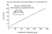
- Fig. 6 illustrates a calculation result of the relationship between the resonance frequency and the driving voltage required to obtain a certain amount of displacement.
- the structure of a movable portion of an actuator is a simple clamped-clamped beam structure.
- the beam is made of AlGaAs with an Al composition of 0.7, the thickness is 250 nanometers, and the air gap is 1.8 micrometers.
- the horizontal axis represents a resonance frequency of the structure when the length of the beam is changed from 20 micrometers to 100 micrometers
- the vertical axis represents a calculated value of the voltage required for a displacement of 0.6 micrometers with respect to the structure. As the length of the beam shortens, the rigidity of the beam becomes higher and the resonance frequency increases.
- the support portion 8 which allows insulation between the beam 9 and the conductive layer 7 is required to have a high breakdown voltage.
- the layer which is to form the support portion 8 is limited to a material of a semi-insulating semiconductor which has an excellent lattice matching property with the semiconductor substrate.
- a semi-insulating semiconductor which has an excellent lattice matching property with a semiconductor substrate has a low breakdown voltage, and there is a problem that the driving voltage cannot be increased.
- the breakdown voltage is 72 V.
- the beam in order to ensure a displacement amount of 0.6 micrometers, the beam will be limited to a beam of a low rigidity with a resonance frequency of approximately 720 kHz or less. Therefore, it is not possible to achieve a higher speed operation.
- the present invention provides a tunable surface emitting laser which is capable of sweeping a wide wavelength range at a high speed with an improved breakdown voltage of a support portion, a manufacturing method of the tunable surface emitting laser, and an optical coherence tomography apparatus including the tunable surface emitting laser.
- a tunable surface emitting laser includes a first reflecting mirror; an active layer on the first reflecting mirror; a conductive layer on the active layer; and a conductive beam which is provided above the conductive layer via a support portion and which comprises a second reflecting mirror. A gap portion is formed between the conductive layer and the conductive beam.
- the conductive layer includes a high resistivity region provided between the support portion and a region which faces the second reflecting mirror.
- a support portion and a region of a conductive layer facing a second reflecting mirror are electrically separated by a high resistivity region which is provided surrounded by the conductive layer. Therefore, the upper limit of the driving voltage that can be applied between a beam and the region facing the second reflecting mirror of the conductive layer can be increased. Consequently, a high-speed tunable surface emitting laser with a wide wavelength variable range can be achieved.
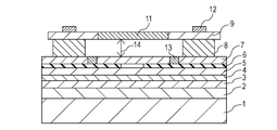
- Fig. 1A is a schematic plan view of Example 1 of a tunable surface emitting laser according to an embodiment of the present invention.
- Fig. 1B is a schematic cross-sectional view of the Example 1 of the tunable surface emitting laser according to the embodiment of the present invention.
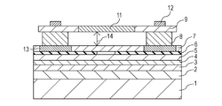
- Fig. 2A is a schematic plan view of Example 2 of the tunable surface emitting laser according to the embodiment of the present invention.
- Fig. 2B is a schematic cross-sectional view of the Example 2 of the tunable surface emitting laser according to the embodiment of the present invention.
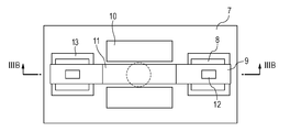
- Fig. 3A is a schematic plan view of Example 3 of the tunable surface emitting laser according to the embodiment of the present invention.
- Fig. 1A is a schematic plan view of Example 1 of a tunable surface emitting laser according to an embodiment of the present invention.
- Fig. 1B is a schematic cross-sectional view of the Example 1 of the tunable surface emitting laser according to the embodiment of the present invention.
- FIG. 3B is a schematic cross-sectional view of the Example 3 of the tunable surface emitting laser according to the embodiment of the present invention.
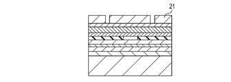
- Fig. 4A is a diagram illustrating a portion of a manufacturing process of a tunable surface emitting laser according to an embodiment of the present invention.
- Fig. 4B is a diagram illustrating a portion of the manufacturing process of the tunable surface emitting laser according to the embodiment of the present invention.
- Fig. 4C is a diagram illustrating a portion of the manufacturing process of the tunable surface emitting laser according to the embodiment of the present invention.
- Fig. 4D is a diagram illustrating a portion of the manufacturing process of the tunable surface emitting laser according to the embodiment of the present invention.
- Fig. 4A is a diagram illustrating a portion of a manufacturing process of a tunable surface emitting laser according to an embodiment of the present invention.
- Fig. 4B is a diagram illustrating a portion of the manufacturing process of the tunable
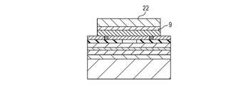
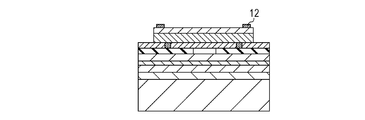
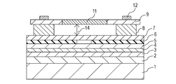
- FIG. 4E is a diagram illustrating a portion of the manufacturing process of the tunable surface emitting laser according to the embodiment of the present invention.
- Fig. 4F is a diagram illustrating a portion of the manufacturing process of the tunable surface emitting laser according to the embodiment of the present invention.
- Fig. 4G is a diagram illustrating a portion of the manufacturing process of the tunable surface emitting laser according to the embodiment of the present invention.
- Fig. 4H is a diagram illustrating a portion of the manufacturing process of the tunable surface emitting laser according to the embodiment of the present invention.
- Fig. 5A is a schematic plan view of a tunable surface emitting laser according to a related art.
- Fig. 5A is a schematic plan view of a tunable surface emitting laser according to a related art.
- FIG. 5B is a schematic cross-sectional view of the tunable surface emitting laser according to the related art.
- Fig. 6 is a diagram illustrating a relationship between a resonance frequency and a voltage required to obtain a certain variable amount.
- Fig. 7 is a schematic diagram of an optical coherence tomography apparatus which is an application example of a tunable surface emitting laser according to an embodiment of the present invention.
- Fig. 1A is a schematic plan view of a tunable surface emitting laser
- Fig. 1B is a schematic cross-sectional view taken along the broken line IB-IB of Fig. 1A.
- a DBR layer 2 which is a first reflecting mirror
- a first spacer layer 3 an active layer 4
- a second spacer layer 5 an insulating layer 6, and a conductive layer 7 are stacked sequentially on a semiconductor substrate 1.
- a first electrode terminal 10 and a support portion 8 to support a beam 9 which includes a second reflecting mirror 11 are provided on the conductive layer 7, and a second electrode terminal 12 is provided on the beam 9.
- the beam 9 and the conductive layer 7 are separated by a gap portion 14 corresponding to the height of the support portion 8.
- the first spacer layer 3 and the second spacer layer 5 have a role of adjusting the optical distance between the first reflecting mirror 2 and the second reflecting mirror 11.
- a semiconductor distributed Bragg reflector (DBR), a dielectric DBR, a high contrast grating (HCG), or the like may be used.
- DBR distributed Bragg reflector
- HCG high contrast grating
- the beam itself it is preferable for the beam itself to have a semiconductor DBR structure.
- a high resistivity region 13 is provided between the region 15 which faces the second reflecting mirror 11 of the conductive layer and the support portion 8, so that the region 15 and the support portion 8 are electrically separated from each other.
- the high resistivity region 13 is provided surrounding the region 15 which includes the first electrode terminal 10 and which faces the second reflecting mirror 11 of the conductive layer.
- the high resistivity region 13 is not limited to this.
- the high resistivity region 13 may be a region which is in contact with the support portion 8 as in Figs. 2A and 2B.
- the high resistivity region 13 may be formed surrounding the periphery of the support portion 8 as in Figs. 3A and 3B.
- the high resistivity region 13 is obtained by increasing the resistivity by implanting ions into the conductive layer 7.
- the purpose of increasing the resistivity of the high resistivity region 13 is to electrically separate the region 15 which faces the second reflecting mirror 11 of the conductive layer and the support portion 8. Therefore, the resistivity of the high resistivity region 13 is set equal to or more than 10 times, and more preferably, equal to or more than 1000 times the resistivity held by the conductive layer 7.
- the conductive layer 7 is made of AlGaAs
- either hydrogen ions, oxygen ions, or boron ions can be preferably used as ions to be implanted into the conductive layer 7.
- An accelerating voltage may be properly selected so that the concentration of ions to be implanted becomes maximum in the vicinity of the depth of the conductive layer 7.
- the dose amount may be selected appropriately in consideration of the required driving voltage, the plane pattern of the high resistivity region 13, and the like, and a range between 1 x 10 12 cm -2 and 5 x 10 15 cm -2 , inclusive, is preferable.
- a method of oxide confinement is also possible.
- a tunable surface emitting laser having a structure according to an embodiment the present invention is able to emit light by sweeping a wide wavelength range at a high speed.
- Fig. 7 illustrates a schematic configuration of an optical coherence tomography apparatus (hereinafter, referred to as OCT apparatus) which can suitably use a tunable surface emitting laser according to an embodiment of the present invention as a light source.
- OCT apparatus optical coherence tomography apparatus
- a tunable surface emitting laser As a wavelength swept light source 501, a tunable surface emitting laser according to an embodiment of the present invention is used.
- a laser beam whose wavelength varies according to the time during which the laser beam is output from the wavelength swept light source 501, passes through a fiber coupler 502 and is split into two parts. One irradiates a subject through a lens. The other transmits through a collimator lens 506, passes through an optical path length adjustment mechanism 507, and transmits through a collimator lens 508, and is then condensed into a fiber.
- Reflected light from the subject is gathered to the fiber coupler via a subject optical path through which the reflected light from the subject transmits. That is, the reflected light transmits through the lens again, returns to the fiber, passes through the fiber coupler 502, and is led to a fiber coupler 504.
- light transmits through a reference light optical path which allows the light to transmit through the optical path length adjustment mechanism and is gathered to the fiber coupler. That is, the light which has passed through the optical path length adjustment mechanism 507 is also gathered to the fiber coupler 504.
- interference unit 504 signal light from the subject and reference light which has passed through the optical path length adjustment mechanism 507 are multiplexed, and an interference signal (interference light) is generated.
- the interference signal is split into two parts at the fiber coupler 504, and only an interference component of the interference signal is detected with a high S/N ratio at a differential detector (light detector) 509.
- the interference signal detected by the differential detector 509 Fourier transform is performed at a processing device 510 on interference spectral data of uniform frequency intervals, and depth information of the subject is thus obtained.
- the obtained depth information is displayed as a tomographic image on an image display device 511.
- Example 1 a tunable surface emitting laser and a manufacturing method of the tunable surface emitting laser according to Example 1 of an embodiment of the present invention will be described.
- a known configuration or method may be applied to a part where a detailed description is omitted.
- Fig. 1A is a schematic plan view of the tunable surface emitting laser according to the Example 1
- Fig. 1B is a schematic cross-sectional view of the tunable surface emitting laser according to the Example 1.
- the semiconductor substrate 1 is provided with the DBR layer 2 which is a first reflecting mirror, the active layer 4 which is arranged above the DBR layer 2 and sandwiched between the first spacer layer 3 and the second spacer layer 5, the insulating layer 6, and the conductive layer 7.
- an n-type GaAs substrate is used as the semiconductor substrate 1.
- the DBR layer 2 has a laminate structure of AlAs and GaAs.
- An InGaAs layer having a multiplequantum well structure is used as the active layer 4, and an AlGaAs layer is used as each of the first spacer layer 3 and the second spacer layer 5.
- an AlGaAs layer which is a semi-insulating semiconductor layer, obtained by oxidizing all the parts of the insulating layer 6 except for the part directly below the second reflecting mirror 11 (round area surrounded by dotted lines in Fig. 1A), is used.
- the beam 9, which is formed of an n-type AlGaAs semiconductor conductive layer with an Al composition of 0.7 with a thickness of approximately 0.25 micrometers, is formed above the conductive layer 7, via the support portion 8 made of semi-insulating GaAs with a thickness of approximately 8 micrometers.
- the HCG 11 is provided which functions as the second reflecting mirror.
- the second electrode terminal 12 which is formed of an AuGe layer with a thickness of approximately 0.2 micrometers, an Ni layer with a thickness of approximately 10 nanometers, and an Au layer with a thickness of approximately 0.3 micrometers, is provided on top of the beam 9.
- the first electrode terminal 10 which is formed of a Ti layer with a thickness of approximately 50 nanometers and an Au layer with a thickness of approximately 0.3 micrometers, is provided on top of the conductive layer 7 such that an area immediately below the beam 9 is avoided.
- the conductive layer 7 is provided with the high resistivity region 13, prepared by ion implantation, which surrounds the region 15 which faces the second reflecting mirror 11 of the conductive layer.
- the support portion 8 is electrically separated from the region 15 which includes the first electrode terminal 10 and which faces the second reflecting mirror 11 of the conductive layer.
- a driving voltage can be applied by wiring which is not illustrated in Figs. 1 A and 1B.
- the beam 9 exhibits the same potential as that of the second electrode terminal 12
- a region of the conductive layer 7 that is surrounded by the high resistivity region 13 exhibits the same potential as that of the first electrode terminal 10.
- This generates an electrostatic force between the beam 9 and the region surrounded by the high resistivity region 13, that is, the region 15 which faces the second reflecting mirror 11 of the conductive layer, causing the beam 9 to be drawn toward the conductive layer 7 and causing a change in the gap portion 14.
- Figs. 4A to 4H illustrate a manufacturing method of the tunable surface emitting laser illustrated in Figs. 1A and 1B by using schematic cross-sectional views.
- the DBR layer 2 which is a first reflecting mirror.
- the first spacer layer 3 which is formed of AlGaAs
- the active layer 4 which is formed of InGaAs
- the second spacer layer 5 which is formed of AlGaAs
- a layer which is formed of AlGaAs are sequentially stacked.
- the layer which is formed of AlGaAs is oxidized except some portions during the process and is prepared as the insulating layer 6.
- a layer (support portion precursor layer) 8' which is to form a support portion and which is formed of semi-insulating GaAs with a thickness of approximately 1.8 micrometers is stacked.
- a layer (beam precursor layer) 9' which is to form a beam and which is formed of n-type AlGaAs with an Al composition of 0.7 with a thickness of approximately 0.25 micrometers is stacked (Fig. 4A).
- the above-described stacked layers are each formed by a metal organic chemical vapor deposition (MOCVD) method.
- a mask 21 for ion implantation is formed of a photoresist (Fig. 4B). Further, proton ions are implanted with an accelerating voltage of 235 keV by a dose amount of 2 x 10 15 cm -2 , and the high resistivity region 13 is formed with a width of 5 micrometers surrounding the region 15 which faces the second reflecting mirror 11 of the conductive layer (Fig. 4C).
- a pattern 22 which covers an HCG pattern that is to function as a second reflecting mirror and a part to be used as a beam is formed by using a resist on top of the layer 9' which is to form a beam.
- Parts of the layer 9', which is to form a beam, and the layer 8', which is to form a support portion, that are not covered with the mask are removed by dry etching until reaching the conductive layer 7, and the layer 9' thereby has a beam shape (Fig. 4E).
- a GaAs layer of the layer 8' which is to form a support portion is subjected to selective etching to pattern the support portion 8, and the gap portion 14 is thereby formed (Fig. 4H).
- a resonance frequency was measured, using a laser Doppler vibrometer, and the measurement result was 1400 kHz.
- a so-called pull-in phenomenon occurred at 125 V.
- no breakdown phenomenon was seen at the support portion 8.
- a tunable surface emitting laser configured according to an embodiment of the present invention is capable of sweeping a wide wavelength range at a high speed and can be suitably used as a light source for an OCT apparatus.
- Substrate 2 First reflecting mirror (DBR layer) 3 First spacer layer 4 Active layer 5 Second spacer layer 6 Insulating layer 7 Conductive layer 8 Support portion 9 Beam 10 First electrode terminal 11 Second reflecting mirror (HCG) 12 Second electrode terminal 13 High resistivity layer 14 Gap portion
Landscapes
- Physics & Mathematics (AREA)
- General Physics & Mathematics (AREA)
- Condensed Matter Physics & Semiconductors (AREA)
- Electromagnetism (AREA)
- Optics & Photonics (AREA)
- Health & Medical Sciences (AREA)
- General Health & Medical Sciences (AREA)
- Nuclear Medicine, Radiotherapy & Molecular Imaging (AREA)
- Radiology & Medical Imaging (AREA)
- Semiconductor Lasers (AREA)
- Instruments For Measurement Of Length By Optical Means (AREA)
- Investigating Or Analysing Materials By Optical Means (AREA)
Abstract
A tunable surface emitting laser includes on a semiconductor substrate (1) a first reflecting mirror (2); an active layer (4) on the first reflecting mirror which may be a DBR; a current confinement layer (6) resulting from partial oxidation of an AlGaAs layer; a conductive layer (7) on the current confinement layer (6) for providing a bias current to the active region; support portions (8) made from electrically insulating material like undoped GaAs; and a conductive film (9) which is provided above the conductive layer via a support portion (8) and which comprises a second reflecting mirror (11) like a HCG. A gap portion (14) is formed between the conductive layer (7) and the conductive film (9). The conductive layer (7) includes a high resistivity region (13) provided between the support portion (8) and the central current guiding region of the current confinement layer (6). Breakdown voltage of the tuning part is increased and rapid wavelength tuning via corresponding currents provided to the electrodes (12) is enabled allowing for faster movement of the second reflector (11).
Description
The present invention relates to a wavelength-variable light source, and more particularly, to a tunable surface emitting laser which moves a reflecting mirror to vary an oscillation wavelength using a microelectromechanical system (MEMS) mechanism as a wavelength variable mechanism.
In recent years, in the medical field, a non-invasive and non-contact diagnostic method called an optical coherence tomographic image diagnostic method (optical coherence tomography, hereinafter abbreviated as OCT), which uses near infrared rays, has been researched. Several approaches have been considered in OCT, with OCT using a wavelength swept light source (swept source optical coherence tomography, hereinafter abbreviated as SS-OCT) attracting attention amongst others. A wavelength-variable light source for SS-OCT requires a wide wavelength variable width, a narrow spectral line width, and a high-speed operation. In order to satisfy such a request, a wavelength-variable vertical cavity surface-emitting laser (hereinafter, abbreviated as a VCSEL) has been researched, in which an oscillation wavelength is varied by changing a cavity length, by moving one reflecting mirror of the VCSEL with an actuator fabricated with the MEMS technique.
As manufacturing methods of such a wavelength-variable VCSEL, there has been a method of fabricating a separate movable portion and bonding the movable portion to a semiconductor laser substrate, and a method of monolithically forming a movable portion on a semiconductor laser substrate. For issues such as the alignment on bonding and for simplicity of the process, the monolithically forming method has been researched more.
NPL 1 discloses a wavelength-variable VCSEL formed monolithically using the MEMS technique. Fig. 5A is a schematic plan view of a tunable surface emitting laser of NPL 1, and Fig. 5B is a schematic cross-sectional view taken along the broken line VB-VB of Fig. 5A. The tunable surface emitting laser is formed by stacking layers in succession from a first reflecting mirror 2 to a layer which is to form a beam 9, which is a movable portion, on a semiconductor substrate 1 and then performing processing such as selective etching to form the beam 9 and to form a first electrode terminal 10 and a second electrode terminal 12. At this time, in order to suppress degradation of an active layer, layers from the first reflecting mirror 2 to the layer which is to form the beam 9 are made of materials lattice-matching with the semiconductor substrate 1.
In NPL 1, GaAs is used for the semiconductor substrate 1. Further, GaAs or AlGaAs is used for each of a distributed Bragg reflector (DBR) layer of the first reflecting mirror 2, a first spacer layer 3, an active layer 4, a second spacer layer 5, an insulating layer 6, and a conductive layer 7. Moreover, GaAs is used for a layer (sacrificial layer) which is to form a support portion 8, and AlGaAs is used for the layer which is to form the beam 9. A high contrast grating (HCG) is formed as a second reflecting mirror 11 on the beam 9.
The conductive layer 7 and the beam 9 are electrically separated from each other via the support portion 8, and when a driving voltage is applied to the conductive layer 7 and the beam 9 via the first electrode terminal 10 and the second electrode terminal 12, respectively, an electrostatic force is generated between the conductive layer 7 and the beam 9. The beam 9 is drawn toward the conductive layer 7 by this electrostatic force, and the cavity length between the second reflecting mirror 11 formed on the beam 9 and the first reflecting mirror 2 changes. Therefore, it is possible to change the oscillation wavelength of the laser.
High Contrast Granting VCSELs: Properties and Implementation on InP-based VCSELs, Technical Report No. UCB/EECS-2011-44
In order to achieve improvement in resolution in the depth direction of a subject and reduction in measurement time, it is required for the wavelength-variable light source for SS-OCT to sweep a wide wavelength range at a high speed. A wavelength variable range is determined by the displacement amount of a beam, and high speed performance is limited by the resonance frequency of the beam.
In an electrostatic actuator, the displacement amount is controlled by a driving voltage applied. A structure with a high resonance frequency has a high rigidity, and a large displacement amount is therefore difficult to obtain with such a structure. Thus, the driving voltage required to obtain a certain amount of displacement becomes higher in a structure with a higher resonance frequency.
As an example, Fig. 6 illustrates a calculation result of the relationship between the resonance frequency and the driving voltage required to obtain a certain amount of displacement. The structure of a movable portion of an actuator is a simple clamped-clamped beam structure. The beam is made of AlGaAs with an Al composition of 0.7, the thickness is 250 nanometers, and the air gap is 1.8 micrometers. In Fig. 6, the horizontal axis represents a resonance frequency of the structure when the length of the beam is changed from 20 micrometers to 100 micrometers, and the vertical axis represents a calculated value of the voltage required for a displacement of 0.6 micrometers with respect to the structure. As the length of the beam shortens, the rigidity of the beam becomes higher and the resonance frequency increases.
As can be seen in Fig. 6, when it is intended to achieve an operation at a high speed while ensuring a certain amount of displacement, it is necessary to increase the driving voltage. In order to increase the driving voltage, the support portion 8 which allows insulation between the beam 9 and the conductive layer 7 is required to have a high breakdown voltage.
However, for monolithic fabrication of the beam 9 on the semiconductor laser substrate, the layer which is to form the support portion 8 is limited to a material of a semi-insulating semiconductor which has an excellent lattice matching property with the semiconductor substrate. Generally, a semi-insulating semiconductor which has an excellent lattice matching property with a semiconductor substrate has a low breakdown voltage, and there is a problem that the driving voltage cannot be increased.
For example, taking the example of GaAs that is used for the support portion in NPL 1, when the air gap is set at 1.8 micrometers, the breakdown voltage is 72 V. In this case, in order to ensure a displacement amount of 0.6 micrometers, the beam will be limited to a beam of a low rigidity with a resonance frequency of approximately 720 kHz or less. Therefore, it is not possible to achieve a higher speed operation.
In view of the above problems, the present invention provides a tunable surface emitting laser which is capable of sweeping a wide wavelength range at a high speed with an improved breakdown voltage of a support portion, a manufacturing method of the tunable surface emitting laser, and an optical coherence tomography apparatus including the tunable surface emitting laser.
A tunable surface emitting laser includes a first reflecting mirror; an active layer on the first reflecting mirror; a conductive layer on the active layer; and a conductive beam which is provided above the conductive layer via a support portion and which comprises a second reflecting mirror. A gap portion is formed between the conductive layer and the conductive beam. The conductive layer includes a high resistivity region provided between the support portion and a region which faces the second reflecting mirror.
According to the present invention, a support portion and a region of a conductive layer facing a second reflecting mirror are electrically separated by a high resistivity region which is provided surrounded by the conductive layer. Therefore, the upper limit of the driving voltage that can be applied between a beam and the region facing the second reflecting mirror of the conductive layer can be increased. Consequently, a high-speed tunable surface emitting laser with a wide wavelength variable range can be achieved.
Further features of the present invention will become apparent from the following description of exemplary embodiments with reference to the attached drawings.
Hereinafter, a tunable surface emitting laser according to embodiments of the present invention will be described, with reference to the accompanying drawings.
Fig. 1A is a schematic plan view of a tunable surface emitting laser, and Fig. 1B is a schematic cross-sectional view taken along the broken line IB-IB of Fig. 1A. In Figs. 1A and 1B, a DBR layer 2 which is a first reflecting mirror, a first spacer layer 3, an active layer 4, a second spacer layer 5, an insulating layer 6, and a conductive layer 7 are stacked sequentially on a semiconductor substrate 1. A first electrode terminal 10 and a support portion 8 to support a beam 9 which includes a second reflecting mirror 11 are provided on the conductive layer 7, and a second electrode terminal 12 is provided on the beam 9. The beam 9 and the conductive layer 7 are separated by a gap portion 14 corresponding to the height of the support portion 8. The first spacer layer 3 and the second spacer layer 5 have a role of adjusting the optical distance between the first reflecting mirror 2 and the second reflecting mirror 11.
As the second reflecting mirror 11, a semiconductor distributed Bragg reflector (DBR), a dielectric DBR, a high contrast grating (HCG), or the like may be used. Particularly, it is preferable to use the HCG, which has a wide reflection band and is structurally lightweight, thus being capable of high-speed operation. In the case of using a semiconductor DBR as a reflecting mirror, it is preferable for the beam itself to have a semiconductor DBR structure.
Further, in an embodiment of the present invention, in order to prevent a driving voltage which is to be applied between the beam 9 and a region 15 which faces the second reflecting mirror 11 of the conductive layer from being applied to the support portion 8, a high resistivity region 13 is provided between the region 15 which faces the second reflecting mirror 11 of the conductive layer and the support portion 8, so that the region 15 and the support portion 8 are electrically separated from each other. In Fig. 1A, the high resistivity region 13 is provided surrounding the region 15 which includes the first electrode terminal 10 and which faces the second reflecting mirror 11 of the conductive layer. However, the high resistivity region 13 is not limited to this. The high resistivity region 13 may be a region which is in contact with the support portion 8 as in Figs. 2A and 2B. Alternatively, the high resistivity region 13 may be formed surrounding the periphery of the support portion 8 as in Figs. 3A and 3B.
The high resistivity region 13 is obtained by increasing the resistivity by implanting ions into the conductive layer 7. The purpose of increasing the resistivity of the high resistivity region 13 is to electrically separate the region 15 which faces the second reflecting mirror 11 of the conductive layer and the support portion 8. Therefore, the resistivity of the high resistivity region 13 is set equal to or more than 10 times, and more preferably, equal to or more than 1000 times the resistivity held by the conductive layer 7.
For example, in the case where the conductive layer 7 is made of AlGaAs, either hydrogen ions, oxygen ions, or boron ions can be preferably used as ions to be implanted into the conductive layer 7. An accelerating voltage may be properly selected so that the concentration of ions to be implanted becomes maximum in the vicinity of the depth of the conductive layer 7. Further, the dose amount may be selected appropriately in consideration of the required driving voltage, the plane pattern of the high resistivity region 13, and the like, and a range between 1 x 1012 cm-2 and 5 x 1015 cm-2, inclusive, is preferable. Moreover, in addition to ion implantation, a method of oxide confinement is also possible.
By electrically separating the region 15 which faces the second reflecting mirror 11 of the conductive layer and the support portion 8, the voltage applied between the region 15 which faces the second reflecting mirror 11 of the conductive layer and the beam 9 is hardly applied to the support portion 8. Therefore, it is possible to apply a voltage which is equal to or higher than the breakdown voltage of the support portion 8 between the region 15 which faces the second reflecting mirror 11 of the conductive layer and the beam 9. Thus, a large displacement is possible even when the beam 9 with a high rigidity is used. That is, a tunable surface emitting laser having a structure according to an embodiment the present invention is able to emit light by sweeping a wide wavelength range at a high speed.
Fig. 7 illustrates a schematic configuration of an optical coherence tomography apparatus (hereinafter, referred to as OCT apparatus) which can suitably use a tunable surface emitting laser according to an embodiment of the present invention as a light source.
As a wavelength swept light source 501, a tunable surface emitting laser according to an embodiment of the present invention is used. A laser beam whose wavelength varies according to the time during which the laser beam is output from the wavelength swept light source 501, passes through a fiber coupler 502 and is split into two parts. One irradiates a subject through a lens. The other transmits through a collimator lens 506, passes through an optical path length adjustment mechanism 507, and transmits through a collimator lens 508, and is then condensed into a fiber.
Reflected light from the subject is gathered to the fiber coupler via a subject optical path through which the reflected light from the subject transmits. That is, the reflected light transmits through the lens again, returns to the fiber, passes through the fiber coupler 502, and is led to a fiber coupler 504.
Further, light transmits through a reference light optical path which allows the light to transmit through the optical path length adjustment mechanism and is gathered to the fiber coupler. That is, the light which has passed through the optical path length adjustment mechanism 507 is also gathered to the fiber coupler 504.
At the fiber coupler (interference unit) 504, signal light from the subject and reference light which has passed through the optical path length adjustment mechanism 507 are multiplexed, and an interference signal (interference light) is generated. The interference signal is split into two parts at the fiber coupler 504, and only an interference component of the interference signal is detected with a high S/N ratio at a differential detector (light detector) 509.
For the interference signal detected by the differential detector 509, Fourier transform is performed at a processing device 510 on interference spectral data of uniform frequency intervals, and depth information of the subject is thus obtained. The obtained depth information is displayed as a tomographic image on an image display device 511.
By using a tunable surface emitting laser according to an embodiment of the present invention as the light source 501, it is possible to provide an OCT apparatus with a high resolution in the depth direction of a subject with a short measurement time.
Hereinafter, a tunable surface emitting laser and a manufacturing method of the tunable surface emitting laser according to Example 1 of an embodiment of the present invention will be described. A known configuration or method may be applied to a part where a detailed description is omitted.
Fig. 1A is a schematic plan view of the tunable surface emitting laser according to the Example 1, and Fig. 1B is a schematic cross-sectional view of the tunable surface emitting laser according to the Example 1. The semiconductor substrate 1 is provided with the DBR layer 2 which is a first reflecting mirror, the active layer 4 which is arranged above the DBR layer 2 and sandwiched between the first spacer layer 3 and the second spacer layer 5, the insulating layer 6, and the conductive layer 7. In the Example 1, an n-type GaAs substrate is used as the semiconductor substrate 1. The DBR layer 2 has a laminate structure of AlAs and GaAs. An InGaAs layer having a multiplequantum well structure is used as the active layer 4, and an AlGaAs layer is used as each of the first spacer layer 3 and the second spacer layer 5. As the insulating layer 6, an AlGaAs layer, which is a semi-insulating semiconductor layer, obtained by oxidizing all the parts of the insulating layer 6 except for the part directly below the second reflecting mirror 11 (round area surrounded by dotted lines in Fig. 1A), is used.
The beam 9, which is formed of an n-type AlGaAs semiconductor conductive layer with an Al composition of 0.7 with a thickness of approximately 0.25 micrometers, is formed above the conductive layer 7, via the support portion 8 made of semi-insulating GaAs with a thickness of approximately 8 micrometers. For the beam 9, the HCG 11 is provided which functions as the second reflecting mirror.
The second electrode terminal 12, which is formed of an AuGe layer with a thickness of approximately 0.2 micrometers, an Ni layer with a thickness of approximately 10 nanometers, and an Au layer with a thickness of approximately 0.3 micrometers, is provided on top of the beam 9. The first electrode terminal 10, which is formed of a Ti layer with a thickness of approximately 50 nanometers and an Au layer with a thickness of approximately 0.3 micrometers, is provided on top of the conductive layer 7 such that an area immediately below the beam 9 is avoided. Further, the conductive layer 7 is provided with the high resistivity region 13, prepared by ion implantation, which surrounds the region 15 which faces the second reflecting mirror 11 of the conductive layer. Thus, the support portion 8 is electrically separated from the region 15 which includes the first electrode terminal 10 and which faces the second reflecting mirror 11 of the conductive layer.
Between the first electrode terminal 10 and the second electrode terminal 12, a driving voltage can be applied by wiring which is not illustrated in Figs. 1 A and 1B. When a driving voltage is applied between the two electrode terminals 10 and 12, the beam 9 exhibits the same potential as that of the second electrode terminal 12, and a region of the conductive layer 7 that is surrounded by the high resistivity region 13 exhibits the same potential as that of the first electrode terminal 10. This generates an electrostatic force between the beam 9 and the region surrounded by the high resistivity region 13, that is, the region 15 which faces the second reflecting mirror 11 of the conductive layer, causing the beam 9 to be drawn toward the conductive layer 7 and causing a change in the gap portion 14.
Next, a manufacturing method of a tunable surface emitting laser according to an embodiment of the present invention will be described with reference to Figs. 4A to 4H. Figs. 4A to 4H illustrate a manufacturing method of the tunable surface emitting laser illustrated in Figs. 1A and 1B by using schematic cross-sectional views.
First, on top of the n-type GaAs semiconductor substrate 1, AlAs and GaAs are stacked alternately to form the DBR layer 2, which is a first reflecting mirror. Then, the first spacer layer 3 which is formed of AlGaAs, the active layer 4 which is formed of InGaAs, the second spacer layer 5 which is formed of AlGaAs, and a layer which is formed of AlGaAs are sequentially stacked. The layer which is formed of AlGaAs is oxidized except some portions during the process and is prepared as the insulating layer 6.
After stacking conductive AlGaAs to form the conductive layer 7 on top of the insulating layer 6, a layer (support portion precursor layer) 8' which is to form a support portion and which is formed of semi-insulating GaAs with a thickness of approximately 1.8 micrometers is stacked. Further, a layer (beam precursor layer) 9' which is to form a beam and which is formed of n-type AlGaAs with an Al composition of 0.7 with a thickness of approximately 0.25 micrometers is stacked (Fig. 4A). The above-described stacked layers are each formed by a metal organic chemical vapor deposition (MOCVD) method.
Next, on top of the layer 9' which is to form a beam, a mask 21 for ion implantation is formed of a photoresist (Fig. 4B). Further, proton ions are implanted with an accelerating voltage of 235 keV by a dose amount of 2 x 1015 cm-2, and the high resistivity region 13 is formed with a width of 5 micrometers surrounding the region 15 which faces the second reflecting mirror 11 of the conductive layer (Fig. 4C).
After removing the ion implantation mask by a solvent (Fig. 4D), a pattern 22 which covers an HCG pattern that is to function as a second reflecting mirror and a part to be used as a beam is formed by using a resist on top of the layer 9' which is to form a beam. Parts of the layer 9', which is to form a beam, and the layer 8', which is to form a support portion, that are not covered with the mask are removed by dry etching until reaching the conductive layer 7, and the layer 9' thereby has a beam shape (Fig. 4E). Thus, through the above-described process, a beam 9 provided with the HCG pattern that functions as the second reflecting mirror, can be formed.
Next, within the region 15 surrounded by the high resistivity region 13 with the exposed conductive layer 7, Ti of approximately 50 nanometers and Au of approximately 300 nanometers are sequentially formed, which are then patterned by using a photolithographic method, to form the first electrode terminal 10 (Fig. 4F). Further, on top of the beam 9, AuGe of approximately 0.2 micrometers, Ni of approximately 10 nanometers, and Au of approximately 300 nanometers are sequentially formed, which are then patterned by using the photolithographic method, to form the second electrode terminal 12 (Fig. 4G).
Finally, by using a mixed solution of citric acid and hydrogen peroxide, a GaAs layer of the layer 8' which is to form a support portion is subjected to selective etching to pattern the support portion 8, and the gap portion 14 is thereby formed (Fig. 4H).
After forming the gap portion 14, a resonance frequency was measured, using a laser Doppler vibrometer, and the measurement result was 1400 kHz. When applying a DC voltage, a so-called pull-in phenomenon occurred at 125 V. However, no breakdown phenomenon was seen at the support portion 8.
In comparison, a sample was fabricated in the same manner as the embodiment except that proton implantation was not performed, and measurement was conducted similarly. It was found that the resonance frequency was 1400 kHz, which is the same as the embodiment. However, a breakdown phenomenon occurred at the support portion 8 at the applied voltage of 70 V.
As is clear from the above result, the configuration of the embodiment of the present invention enables application of a voltage higher than the breakdown voltage of the support portion 8, onto the beam 9 and the region 15 facing the second reflecting mirror of the conductive layer, and allows a large displacement even using the beam 9 with a high rigidity. Therefore, a tunable surface emitting laser configured according to an embodiment of the present invention is capable of sweeping a wide wavelength range at a high speed and can be suitably used as a light source for an OCT apparatus.
While the present invention has been described with reference to exemplary embodiments, it is to be understood that the invention is not limited to the disclosed exemplary embodiments. The scope of the following claims is to be accorded the broadest interpretation so as to encompass all such modifications and equivalent structures and functions.
This application claims the benefit of Japanese Patent Application No. 2013-247128, filed November 29, 2013, which is hereby incorporated by reference herein in its entirety.
1 Substrate
2 First reflecting mirror (DBR layer)
3 First spacer layer
4 Active layer
5 Second spacer layer
6 Insulating layer
7 Conductive layer
8 Support portion
9 Beam
10 First electrode terminal
11 Second reflecting mirror (HCG)
12 Second electrode terminal
13 High resistivity layer
14 Gap portion
2 First reflecting mirror (DBR layer)
3 First spacer layer
4 Active layer
5 Second spacer layer
6 Insulating layer
7 Conductive layer
8 Support portion
9 Beam
10 First electrode terminal
11 Second reflecting mirror (HCG)
12 Second electrode terminal
13 High resistivity layer
14 Gap portion
Claims (11)
- A tunable surface emitting laser comprising:
a first reflecting mirror;
an active layer on the first reflecting mirror;
a conductive layer on the active layer; and
a conductive beam which is provided above the conductive layer via a support portion and which comprises a second reflecting mirror,
wherein a gap portion is formed between the conductive layer and the conductive beam, and
wherein the conductive layer includes a high resistivity region provided between the support portion and a region which faces the second reflecting mirror. - The tunable surface emitting laser according to Claim 1, wherein a resistivity of the high resistivity region is equal to or more than ten times a resistivity of the conductive layer.
- The tunable surface emitting laser according to Claim 1 or 2, wherein the high resistivity region is a region where ions are implanted into the conductive layer.
- The tunable surface emitting laser according to Claim 3, wherein the ions implanted to the high resistivity region are either hydrogen ions or oxygen ions.
- The tunable surface emitting laser according to any one of Claims 1 to 4, wherein the second reflecting mirror is a high contrast grating.
- The tunable surface emitting laser according to any one of Claims 1 to 5, wherein the first reflecting mirror is a distributed Bragg reflector.
- An optical coherence tomography apparatus comprising:
a light source;
a subject optical path through which a subject is irradiated with light from the light source and through which reflecting light from the subject transmits;
a reference light optical path through which the light from the light source transmits by allowing the light to pass through an optical path length adjustment mechanism;
an interference unit which causes reflecting light from the subject optical path and light from the reference light optical path to interfere with each other;
a light detector which detects interference light from the interference unit; and
a processing device which acquires a tomographic image of the subject from an interference signal obtained by the light detector,
wherein the light source includes the tunable surface emitting laser according to any one of Claims 1 to 6. - A manufacturing method of a tunable surface emitting laser, the method comprising:
a step of sequentially forming a conductive layer, a support portion precursor layer, and a conductive beam precursor layer on a substrate including a first reflecting mirror and an active layer;
a step of forming a high resistivity region by increasing a resistivity of a part of the conductive layer;
a step of patterning the support portion precursor layer and the beam precursor layer;
a step of forming a second reflecting mirror in the beam precursor layer; and
a step of removing a part of the support portion precursor layer to form a conductive beam and a gap portion between the conductive beam and the conductive layer. - The manufacturing method of the tunable surface emitting laser according to Claim 8, wherein the step of increasing the resistivity of the part of the conductive layer is performed by ion implantation.
- The manufacturing method of the tunable surface emitting laser according to Claim 9, wherein the step of increasing the resistivity of the part of the conductive layer is performed by implanting hydrogen ions or oxygen ions.
- The manufacturing method of the tunable surface emitting laser according to any one of Claims 8 to 10, wherein the high resistivity region is formed between a region facing a part which is to be the second reflecting mirror in the beam precursor layer and a part which is to be a support portion in the support portion precursor layer.
Applications Claiming Priority (2)
| Application Number | Priority Date | Filing Date | Title |
|---|---|---|---|
| JP2013-247128 | 2013-11-29 | ||
| JP2013247128A JP2015106607A (en) | 2013-11-29 | 2013-11-29 | Wavelength variable service emitting laser and manufacturing method therefor, and optical interference tomographic image acquisition device |
Publications (1)
| Publication Number | Publication Date |
|---|---|
| WO2015079636A1 true WO2015079636A1 (en) | 2015-06-04 |
Family
ID=52023589
Family Applications (1)
| Application Number | Title | Priority Date | Filing Date |
|---|---|---|---|
| PCT/JP2014/005693 Ceased WO2015079636A1 (en) | 2013-11-29 | 2014-11-13 | Tunable surface emitting laser, manufacturing method thereof, and optical coherence tomography apparatus including tunable surface emitting laser |
Country Status (2)
| Country | Link |
|---|---|
| JP (1) | JP2015106607A (en) |
| WO (1) | WO2015079636A1 (en) |
Families Citing this family (3)
| Publication number | Priority date | Publication date | Assignee | Title |
|---|---|---|---|---|
| JP6608202B2 (en) * | 2015-07-13 | 2019-11-20 | キヤノン株式会社 | Surface emitting laser, information acquisition device, and imaging device |
| JP6608203B2 (en) * | 2015-07-13 | 2019-11-20 | キヤノン株式会社 | Surface emitting laser, information acquisition device, and imaging device |
| JP7396643B2 (en) * | 2019-12-13 | 2023-12-12 | 国立研究開発法人情報通信研究機構 | Tunable surface emitting laser |
Citations (3)
| Publication number | Priority date | Publication date | Assignee | Title |
|---|---|---|---|---|
| US20020150130A1 (en) * | 2001-04-16 | 2002-10-17 | Coldren Larry A. | Tunable VCSEL assembly |
| US20080159468A1 (en) * | 2006-04-11 | 2008-07-03 | Changho Chong | Optical coherent tomography |
| KR20140036789A (en) * | 2012-09-18 | 2014-03-26 | 한국전자통신연구원 | Vertical-cavity surface emitting laser and manufacturing method for the same |
-
2013
- 2013-11-29 JP JP2013247128A patent/JP2015106607A/en active Pending
-
2014
- 2014-11-13 WO PCT/JP2014/005693 patent/WO2015079636A1/en not_active Ceased
Patent Citations (3)
| Publication number | Priority date | Publication date | Assignee | Title |
|---|---|---|---|---|
| US20020150130A1 (en) * | 2001-04-16 | 2002-10-17 | Coldren Larry A. | Tunable VCSEL assembly |
| US20080159468A1 (en) * | 2006-04-11 | 2008-07-03 | Changho Chong | Optical coherent tomography |
| KR20140036789A (en) * | 2012-09-18 | 2014-03-26 | 한국전자통신연구원 | Vertical-cavity surface emitting laser and manufacturing method for the same |
Non-Patent Citations (3)
| Title |
|---|
| HAYATO SANO ET AL: "Wavelength Trimming of Micro-Machined VCSELs", IEICE TRANSACTIONS ON ELECTRONICS, INSTITUTE OF ELECTRONICS, TOKYO, JP, vol. E95C, no. 2, 1 February 2012 (2012-02-01), pages 237 - 242, XP001573141, ISSN: 0916-8524, [retrieved on 20120201], DOI: 10.1587/TRANSELE.E95.C.237 * |
| UNKNOWN: "High Contrast Granting VCSELs: Properties and Implementation on InP-based VCSELs,", TECHNICAL REPORT NO. UCB/EECS-2011-44 |
| WU M S ET AL: "TUNABLE MICROMACHINED VERTICAL CAVITY SURFACE EMITTING LASER", ELECTRONICS LETTERS, IEE STEVENAGE, GB, vol. 31, no. 19, 14 September 1995 (1995-09-14), XP000530390, ISSN: 0013-5194, DOI: 10.1049/EL:19951159 * |
Also Published As
| Publication number | Publication date |
|---|---|
| JP2015106607A (en) | 2015-06-08 |
Similar Documents
| Publication | Publication Date | Title |
|---|---|---|
| US10128637B2 (en) | Wavelength-tunable vertical cavity surface emitting laser for swept source optical coherence tomography system | |
| US9709381B2 (en) | Surface emitting laser and optical coherence tomography apparatus including the same | |
| CN106207750A (en) | Surface emitting laser and the optical coherence tomographic imaging apparatus comprising it | |
| US10490978B2 (en) | Surface emitting laser, information obtaining apparatus, and imaging apparatus | |
| WO2015079636A1 (en) | Tunable surface emitting laser, manufacturing method thereof, and optical coherence tomography apparatus including tunable surface emitting laser | |
| EP2775574A2 (en) | Surface emitting laser and optical coherence tomography apparatus equipped with surface emitting laser | |
| US9379520B2 (en) | Surface emitting laser and optical coherence tomography apparatus | |
| US9972971B2 (en) | Surface emitting laser, information acquisition apparatus, and imaging apparatus | |
| EP3878066B1 (en) | Bonded tunable vcsel with bi-directional actuation | |
| US9991675B2 (en) | Surface emitting laser, laser array, light source device, information acquisition device, and optical coherence tomography apparatus | |
| JP6608203B2 (en) | Surface emitting laser, information acquisition device, and imaging device | |
| US20150146212A1 (en) | Surface emitting laser and optical coherence tomography apparatus including the same | |
| JP6608202B2 (en) | Surface emitting laser, information acquisition device, and imaging device | |
| JP6650961B2 (en) | Surface emitting laser and optical coherence tomography using the same | |
| US20150049342A1 (en) | Surface light-emitting laser and optical coherence tomographic imaging apparatus having the same | |
| WO2016103604A1 (en) | Surface emitting laser, information acquiring apparatus, imaging apparatus, laser array, and method of manufacturing surface emitting laser | |
| US10418784B2 (en) | Surface emitting laser, information acquiring apparatus, imaging apparatus, laser array, and method of manufacturing surface emitting laser | |
| HK1224090B (en) | Wavelength-tunable vertical cavity surface emitting laser for swept source optical coherence tomography system |
Legal Events
| Date | Code | Title | Description |
|---|---|---|---|
| 121 | Ep: the epo has been informed by wipo that ep was designated in this application |
Ref document number: 14811996 Country of ref document: EP Kind code of ref document: A1 |
|
| NENP | Non-entry into the national phase |
Ref country code: DE |
|
| 122 | Ep: pct application non-entry in european phase |
Ref document number: 14811996 Country of ref document: EP Kind code of ref document: A1 |