WO2014199975A1 - Window material for ultraviolet-ray-emitting element and method for producing same - Google Patents
Window material for ultraviolet-ray-emitting element and method for producing same Download PDFInfo
- Publication number
- WO2014199975A1 WO2014199975A1 PCT/JP2014/065317 JP2014065317W WO2014199975A1 WO 2014199975 A1 WO2014199975 A1 WO 2014199975A1 JP 2014065317 W JP2014065317 W JP 2014065317W WO 2014199975 A1 WO2014199975 A1 WO 2014199975A1
- Authority
- WO
- WIPO (PCT)
- Prior art keywords
- ultraviolet light
- window material
- light emitting
- emitting element
- substrate
- Prior art date
Links
Images


Classifications
-
- C—CHEMISTRY; METALLURGY
- C04—CEMENTS; CONCRETE; ARTIFICIAL STONE; CERAMICS; REFRACTORIES
- C04B—LIME, MAGNESIA; SLAG; CEMENTS; COMPOSITIONS THEREOF, e.g. MORTARS, CONCRETE OR LIKE BUILDING MATERIALS; ARTIFICIAL STONE; CERAMICS; REFRACTORIES; TREATMENT OF NATURAL STONE
- C04B35/00—Shaped ceramic products characterised by their composition; Ceramics compositions; Processing powders of inorganic compounds preparatory to the manufacturing of ceramic products
- C04B35/01—Shaped ceramic products characterised by their composition; Ceramics compositions; Processing powders of inorganic compounds preparatory to the manufacturing of ceramic products based on oxide ceramics
- C04B35/10—Shaped ceramic products characterised by their composition; Ceramics compositions; Processing powders of inorganic compounds preparatory to the manufacturing of ceramic products based on oxide ceramics based on aluminium oxide
- C04B35/111—Fine ceramics
- C04B35/115—Translucent or transparent products
-
- B—PERFORMING OPERATIONS; TRANSPORTING
- B29—WORKING OF PLASTICS; WORKING OF SUBSTANCES IN A PLASTIC STATE IN GENERAL
- B29B—PREPARATION OR PRETREATMENT OF THE MATERIAL TO BE SHAPED; MAKING GRANULES OR PREFORMS; RECOVERY OF PLASTICS OR OTHER CONSTITUENTS OF WASTE MATERIAL CONTAINING PLASTICS
- B29B11/00—Making preforms
- B29B11/14—Making preforms characterised by structure or composition
-
- B—PERFORMING OPERATIONS; TRANSPORTING
- B29—WORKING OF PLASTICS; WORKING OF SUBSTANCES IN A PLASTIC STATE IN GENERAL
- B29C—SHAPING OR JOINING OF PLASTICS; SHAPING OF MATERIAL IN A PLASTIC STATE, NOT OTHERWISE PROVIDED FOR; AFTER-TREATMENT OF THE SHAPED PRODUCTS, e.g. REPAIRING
- B29C49/00—Blow-moulding, i.e. blowing a preform or parison to a desired shape within a mould; Apparatus therefor
- B29C49/071—Preforms or parisons characterised by their configuration, e.g. geometry, dimensions or physical properties
-
- C—CHEMISTRY; METALLURGY
- C04—CEMENTS; CONCRETE; ARTIFICIAL STONE; CERAMICS; REFRACTORIES
- C04B—LIME, MAGNESIA; SLAG; CEMENTS; COMPOSITIONS THEREOF, e.g. MORTARS, CONCRETE OR LIKE BUILDING MATERIALS; ARTIFICIAL STONE; CERAMICS; REFRACTORIES; TREATMENT OF NATURAL STONE
- C04B35/00—Shaped ceramic products characterised by their composition; Ceramics compositions; Processing powders of inorganic compounds preparatory to the manufacturing of ceramic products
- C04B35/622—Forming processes; Processing powders of inorganic compounds preparatory to the manufacturing of ceramic products
- C04B35/626—Preparing or treating the powders individually or as batches ; preparing or treating macroscopic reinforcing agents for ceramic products, e.g. fibres; mechanical aspects section B
- C04B35/62605—Treating the starting powders individually or as mixtures
- C04B35/62645—Thermal treatment of powders or mixtures thereof other than sintering
- C04B35/62655—Drying, e.g. freeze-drying, spray-drying, microwave or supercritical drying
-
- C—CHEMISTRY; METALLURGY
- C04—CEMENTS; CONCRETE; ARTIFICIAL STONE; CERAMICS; REFRACTORIES
- C04B—LIME, MAGNESIA; SLAG; CEMENTS; COMPOSITIONS THEREOF, e.g. MORTARS, CONCRETE OR LIKE BUILDING MATERIALS; ARTIFICIAL STONE; CERAMICS; REFRACTORIES; TREATMENT OF NATURAL STONE
- C04B35/00—Shaped ceramic products characterised by their composition; Ceramics compositions; Processing powders of inorganic compounds preparatory to the manufacturing of ceramic products
- C04B35/622—Forming processes; Processing powders of inorganic compounds preparatory to the manufacturing of ceramic products
- C04B35/626—Preparing or treating the powders individually or as batches ; preparing or treating macroscopic reinforcing agents for ceramic products, e.g. fibres; mechanical aspects section B
- C04B35/63—Preparing or treating the powders individually or as batches ; preparing or treating macroscopic reinforcing agents for ceramic products, e.g. fibres; mechanical aspects section B using additives specially adapted for forming the products, e.g.. binder binders
- C04B35/632—Organic additives
- C04B35/634—Polymers
-
- C—CHEMISTRY; METALLURGY
- C04—CEMENTS; CONCRETE; ARTIFICIAL STONE; CERAMICS; REFRACTORIES
- C04B—LIME, MAGNESIA; SLAG; CEMENTS; COMPOSITIONS THEREOF, e.g. MORTARS, CONCRETE OR LIKE BUILDING MATERIALS; ARTIFICIAL STONE; CERAMICS; REFRACTORIES; TREATMENT OF NATURAL STONE
- C04B35/00—Shaped ceramic products characterised by their composition; Ceramics compositions; Processing powders of inorganic compounds preparatory to the manufacturing of ceramic products
- C04B35/622—Forming processes; Processing powders of inorganic compounds preparatory to the manufacturing of ceramic products
- C04B35/626—Preparing or treating the powders individually or as batches ; preparing or treating macroscopic reinforcing agents for ceramic products, e.g. fibres; mechanical aspects section B
- C04B35/63—Preparing or treating the powders individually or as batches ; preparing or treating macroscopic reinforcing agents for ceramic products, e.g. fibres; mechanical aspects section B using additives specially adapted for forming the products, e.g.. binder binders
- C04B35/638—Removal thereof
-
- G—PHYSICS
- G02—OPTICS
- G02B—OPTICAL ELEMENTS, SYSTEMS OR APPARATUS
- G02B1/00—Optical elements characterised by the material of which they are made; Optical coatings for optical elements
- G02B1/10—Optical coatings produced by application to, or surface treatment of, optical elements
- G02B1/12—Optical coatings produced by application to, or surface treatment of, optical elements by surface treatment, e.g. by irradiation
-
- G—PHYSICS
- G02—OPTICS
- G02B—OPTICAL ELEMENTS, SYSTEMS OR APPARATUS
- G02B5/00—Optical elements other than lenses
- G02B5/02—Diffusing elements; Afocal elements
- G02B5/0205—Diffusing elements; Afocal elements characterised by the diffusing properties
- G02B5/0236—Diffusing elements; Afocal elements characterised by the diffusing properties the diffusion taking place within the volume of the element
- G02B5/0242—Diffusing elements; Afocal elements characterised by the diffusing properties the diffusion taking place within the volume of the element by means of dispersed particles
-
- G—PHYSICS
- G02—OPTICS
- G02B—OPTICAL ELEMENTS, SYSTEMS OR APPARATUS
- G02B5/00—Optical elements other than lenses
- G02B5/02—Diffusing elements; Afocal elements
- G02B5/0273—Diffusing elements; Afocal elements characterized by the use
- G02B5/0278—Diffusing elements; Afocal elements characterized by the use used in transmission
-
- B—PERFORMING OPERATIONS; TRANSPORTING
- B29—WORKING OF PLASTICS; WORKING OF SUBSTANCES IN A PLASTIC STATE IN GENERAL
- B29C—SHAPING OR JOINING OF PLASTICS; SHAPING OF MATERIAL IN A PLASTIC STATE, NOT OTHERWISE PROVIDED FOR; AFTER-TREATMENT OF THE SHAPED PRODUCTS, e.g. REPAIRING
- B29C2949/00—Indexing scheme relating to blow-moulding
- B29C2949/07—Preforms or parisons characterised by their configuration
- B29C2949/0715—Preforms or parisons characterised by their configuration the preform having one end closed
-
- B—PERFORMING OPERATIONS; TRANSPORTING
- B29—WORKING OF PLASTICS; WORKING OF SUBSTANCES IN A PLASTIC STATE IN GENERAL
- B29K—INDEXING SCHEME ASSOCIATED WITH SUBCLASSES B29B, B29C OR B29D, RELATING TO MOULDING MATERIALS OR TO MATERIALS FOR MOULDS, REINFORCEMENTS, FILLERS OR PREFORMED PARTS, e.g. INSERTS
- B29K2505/00—Use of metals, their alloys or their compounds, as filler
- B29K2505/02—Aluminium
-
- B—PERFORMING OPERATIONS; TRANSPORTING
- B29—WORKING OF PLASTICS; WORKING OF SUBSTANCES IN A PLASTIC STATE IN GENERAL
- B29L—INDEXING SCHEME ASSOCIATED WITH SUBCLASS B29C, RELATING TO PARTICULAR ARTICLES
- B29L2011/00—Optical elements, e.g. lenses, prisms
-
- C—CHEMISTRY; METALLURGY
- C04—CEMENTS; CONCRETE; ARTIFICIAL STONE; CERAMICS; REFRACTORIES
- C04B—LIME, MAGNESIA; SLAG; CEMENTS; COMPOSITIONS THEREOF, e.g. MORTARS, CONCRETE OR LIKE BUILDING MATERIALS; ARTIFICIAL STONE; CERAMICS; REFRACTORIES; TREATMENT OF NATURAL STONE
- C04B2235/00—Aspects relating to ceramic starting mixtures or sintered ceramic products
- C04B2235/02—Composition of constituents of the starting material or of secondary phases of the final product
- C04B2235/50—Constituents or additives of the starting mixture chosen for their shape or used because of their shape or their physical appearance
- C04B2235/54—Particle size related information
- C04B2235/5409—Particle size related information expressed by specific surface values
-
- C—CHEMISTRY; METALLURGY
- C04—CEMENTS; CONCRETE; ARTIFICIAL STONE; CERAMICS; REFRACTORIES
- C04B—LIME, MAGNESIA; SLAG; CEMENTS; COMPOSITIONS THEREOF, e.g. MORTARS, CONCRETE OR LIKE BUILDING MATERIALS; ARTIFICIAL STONE; CERAMICS; REFRACTORIES; TREATMENT OF NATURAL STONE
- C04B2235/00—Aspects relating to ceramic starting mixtures or sintered ceramic products
- C04B2235/60—Aspects relating to the preparation, properties or mechanical treatment of green bodies or pre-forms
- C04B2235/602—Making the green bodies or pre-forms by moulding
- C04B2235/6023—Gel casting
-
- C—CHEMISTRY; METALLURGY
- C04—CEMENTS; CONCRETE; ARTIFICIAL STONE; CERAMICS; REFRACTORIES
- C04B—LIME, MAGNESIA; SLAG; CEMENTS; COMPOSITIONS THEREOF, e.g. MORTARS, CONCRETE OR LIKE BUILDING MATERIALS; ARTIFICIAL STONE; CERAMICS; REFRACTORIES; TREATMENT OF NATURAL STONE
- C04B2235/00—Aspects relating to ceramic starting mixtures or sintered ceramic products
- C04B2235/60—Aspects relating to the preparation, properties or mechanical treatment of green bodies or pre-forms
- C04B2235/602—Making the green bodies or pre-forms by moulding
- C04B2235/6025—Tape casting, e.g. with a doctor blade
-
- C—CHEMISTRY; METALLURGY
- C04—CEMENTS; CONCRETE; ARTIFICIAL STONE; CERAMICS; REFRACTORIES
- C04B—LIME, MAGNESIA; SLAG; CEMENTS; COMPOSITIONS THEREOF, e.g. MORTARS, CONCRETE OR LIKE BUILDING MATERIALS; ARTIFICIAL STONE; CERAMICS; REFRACTORIES; TREATMENT OF NATURAL STONE
- C04B2235/00—Aspects relating to ceramic starting mixtures or sintered ceramic products
- C04B2235/70—Aspects relating to sintered or melt-casted ceramic products
- C04B2235/72—Products characterised by the absence or the low content of specific components, e.g. alkali metal free alumina ceramics
-
- C—CHEMISTRY; METALLURGY
- C04—CEMENTS; CONCRETE; ARTIFICIAL STONE; CERAMICS; REFRACTORIES
- C04B—LIME, MAGNESIA; SLAG; CEMENTS; COMPOSITIONS THEREOF, e.g. MORTARS, CONCRETE OR LIKE BUILDING MATERIALS; ARTIFICIAL STONE; CERAMICS; REFRACTORIES; TREATMENT OF NATURAL STONE
- C04B2235/00—Aspects relating to ceramic starting mixtures or sintered ceramic products
- C04B2235/70—Aspects relating to sintered or melt-casted ceramic products
- C04B2235/74—Physical characteristics
- C04B2235/78—Grain sizes and shapes, product microstructures, e.g. acicular grains, equiaxed grains, platelet-structures
- C04B2235/786—Micrometer sized grains, i.e. from 1 to 100 micron
-
- C—CHEMISTRY; METALLURGY
- C04—CEMENTS; CONCRETE; ARTIFICIAL STONE; CERAMICS; REFRACTORIES
- C04B—LIME, MAGNESIA; SLAG; CEMENTS; COMPOSITIONS THEREOF, e.g. MORTARS, CONCRETE OR LIKE BUILDING MATERIALS; ARTIFICIAL STONE; CERAMICS; REFRACTORIES; TREATMENT OF NATURAL STONE
- C04B2235/00—Aspects relating to ceramic starting mixtures or sintered ceramic products
- C04B2235/70—Aspects relating to sintered or melt-casted ceramic products
- C04B2235/95—Products characterised by their size, e.g. microceramics
-
- C—CHEMISTRY; METALLURGY
- C04—CEMENTS; CONCRETE; ARTIFICIAL STONE; CERAMICS; REFRACTORIES
- C04B—LIME, MAGNESIA; SLAG; CEMENTS; COMPOSITIONS THEREOF, e.g. MORTARS, CONCRETE OR LIKE BUILDING MATERIALS; ARTIFICIAL STONE; CERAMICS; REFRACTORIES; TREATMENT OF NATURAL STONE
- C04B2235/00—Aspects relating to ceramic starting mixtures or sintered ceramic products
- C04B2235/70—Aspects relating to sintered or melt-casted ceramic products
- C04B2235/96—Properties of ceramic products, e.g. mechanical properties such as strength, toughness, wear resistance
- C04B2235/963—Surface properties, e.g. surface roughness
Definitions
- the present invention relates to a window material for an ultraviolet light emitting element having good ultraviolet light transmittance from an ultraviolet light emitting element such as a light emitting diode, a laser diode, or a discharge lamp emitting an ultraviolet ray having a wavelength of 300 nm or less.
- an ultraviolet light emitting element such as a light emitting diode, a laser diode, or a discharge lamp emitting an ultraviolet ray having a wavelength of 300 nm or less.
- UV-C Ultraviolet light is used according to the length of its wavelength, and in particular, light in the wavelength range of 280 nm or less is called UV-C, and is used for sterilization and sterilization because it is highly bactericidal ( See JP 2008-091623 A).
- An ultraviolet light emitting element is mentioned as one of the light sources which emit an ultraviolet ray, and the ultraviolet light emitting element is covered with a translucent material as a window material for protection of the element.
- a glass material is used as a translucent material for the ultraviolet light emitting element, and high silica glass (quartz) or the like is used from the viewpoints of productivity, cost, and strength (see JP-A-2000-349348). ).
- quartz is used as a window material for an ultraviolet light emitting element, but quartz has a thermal conductivity as low as about 1 W / m ⁇ K. Therefore, the heat can not be dissipated efficiently, and there is a concern that the damage due to the temperature rise of the ultraviolet light emitting element and the deterioration are likely to occur.
- the forward total light transmittance decreases as the wavelength decreases. In particular, it is remarkable at 300 nm or less.
- the present invention has been made in consideration of such problems, and has a high thermal conductivity and can ensure a high transmittance to ultraviolet light of 300 nm or less, and is suitable for use in an ultraviolet light emitting element.
- An object of the present invention is to provide a window material for an ultraviolet light emitting element and a method of manufacturing the same.
- a window material for an ultraviolet light emitting device is a window material for an ultraviolet light emitting device disposed at least on the ultraviolet light emitting side of an ultraviolet light emitting device emitting ultraviolet light having a wavelength of 300 nm or less And has an average particle size of 6 to 60 ⁇ m on the surface.
- the substrate may have a plate shape having a thickness of 2.0 mm or less and have one surface and the other surface opposite to the one surface. .
- the thickness described above may be 1.5 mm or less, or 1.0 mm or less. Preferably it is 0.5 mm or less, More preferably, it is 0.3 mm or less.
- the other surface may be a surface on the ultraviolet incident side, and at least the other surface may have a surface roughness Ra of 0.2 ⁇ m or more. Preferably, it is 0.2 to 0.6 ⁇ m.
- the surface roughness of the one surface of the substrate is preferably different from the surface roughness of the other surface.
- the one surface is the surface on the ultraviolet light emission side
- the other surface is the surface on the ultraviolet light incidence side
- a method of manufacturing a window material for an ultraviolet light emitting element according to the second invention is a method of manufacturing a window material for an ultraviolet light emitting element for manufacturing a window material for an ultraviolet light emitting element according to the first invention described above
- the method is characterized in that it comprises a step of producing a substrate made of translucent alumina and having one surface and the other surface opposite to the one surface by a gel cast method or a tape forming method.
- the surface roughness of the one surface of the substrate may be made different from the surface roughness of the other surface.
- one surface or the other surface of the substrate may be mirror-polished, or one surface or the other surface of the substrate may be ground.
- the second invention may further include the step of mirror-polishing at least the one surface of the substrate to a surface roughness Ra of 0.03 ⁇ m or less.
- the surface roughness of at least the other surface of the substrate may be further increased.
- This treatment includes grinding at least the other surface of the substrate.
- baking of different types of setters may be brought into contact with one side and the other side of the molded body during baking of the molded body.
- the surface roughness of the other surface of the substrate may be increased by using, as a setter in contact with the other surface, a setter whose surface roughness is larger than that in contact with one surface.
- the method further comprises the step of mirror-polishing the one surface of the substrate to a surface roughness Ra of 0.03 ⁇ m or less, and further increasing the surface roughness of the other surface of the substrate Processing may be performed.
- This treatment includes grinding at least the other surface of the substrate.
- the window material for an ultraviolet light emitting element According to the window material for an ultraviolet light emitting element according to the present invention, high transmittance can be secured for ultraviolet light of 300 nm or less, and a window material suitable for the ultraviolet light emitting element can be obtained. Moreover, since the light-transmissive alumina substrate has a high thermal conductivity of 30 W / m ⁇ K or more, it can efficiently dissipate the heat generated by the drive of the ultraviolet light emitting element, and the temperature rise in the ultraviolet light emitting element It is possible to avoid damage or deterioration.
- the window material for an ultraviolet light emitting device according to the present invention, high transmittance can be secured for ultraviolet light of 300 nm or less, and heat generated by driving the ultraviolet light emitting device can be efficiently obtained.
- a window material that can dissipate heat can be easily manufactured.
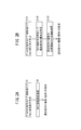
- FIG. 1 is a cross-sectional view showing a window material for an ultraviolet light emitting element according to the present embodiment.
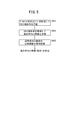
- FIG. 2A is a process diagram showing a first method of manufacturing a window material for an ultraviolet light emitting element
- FIG. 2B is a process diagram showing a second manufacturing method.
- FIG. 3A is a process diagram showing a third method of manufacturing a window material for an ultraviolet light emitting element
- FIG. 3B is a process diagram showing a fourth manufacturing method.
- FIG. 4A is a process diagram showing a fifth method of manufacturing the window material for ultraviolet light emitting elements
- FIG. 4B is a process diagram showing the sixth manufacturing method.
- FIG. 5 is process drawing which shows the 7th manufacturing method of the window material for ultraviolet light emitting elements.
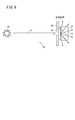
- FIG. 6 is an explanatory view showing a method of evaluating the front total light transmittance in Examples 1 to 6 and Comparative Examples 1 to 3.
- FIGS. 1 to 6 embodiments of the window material for an ultraviolet light emitting element according to the present invention and the method for manufacturing the same will be described with reference to FIGS. 1 to 6.
- “to” indicating a numerical range is used as a meaning including the numerical values described before and after it as the lower limit value and the upper limit value.
- the window material for ultraviolet light emitting element (hereinafter referred to simply as window material 10) according to the present embodiment is high in ultraviolet light 12 from an ultraviolet light emitting element (not shown) that emits ultraviolet light having a wavelength of 300 nm or less. Permeate through.
- the window member 10 is formed of an alumina substrate (light transmitting alumina substrate 14).
- the translucent alumina substrate 14 faces the surface from which the ultraviolet light 12 is emitted (the emission side surface 16a: one surface), and the surface on the side where the ultraviolet light 12 is incident (the incident side 16b: the other surface). And has a thickness t of 0.3 mm or less.
- the planar shape of each plate surface includes, for example, a triangular shape, a rectangular shape, a square shape, a circular shape, an elliptical shape, a polygonal shape, and the like depending on the shape of the case where the ultraviolet light emitting element is mounted.
- the average particle diameter of the surface of the translucent alumina substrate 14 is preferably 6 to 60 ⁇ m, more preferably 6 to 20 ⁇ m.
- the measurement method of the average particle diameter of the surface was performed as follows. That is, an arbitrary part of the surface was observed by magnifying it by 200 times with an optical microscope, and the number of crystals located on a 0.7 mm line segment was counted. Then, the value obtained by dividing the value obtained by multiplying 0.7 by 4 / ⁇ by the number of crystals is defined as the average particle size.
- the surface roughness of the emission side surface 16 a of the translucent alumina substrate 14 and the surface roughness of the incidence side surface 16 b are different.
- each surface roughness of the emission side surface 16a and the incidence side surface 16b is different. May be
- the method for producing the translucent alumina substrate 14 is not particularly limited, but any method such as a doctor blade method (tape molding method), an extrusion method, a gel cast method, etc. may be used.
- the light-transmissive alumina substrate 14 is produced by using a gel cast method or a tape forming method, and particularly preferably using a gel cast method.
- a raw material powder (ceramic powder) containing alumina powder, a slurry containing a dispersion medium and a gelling agent is cast in a mold, and the slurry is gelled to obtain a molded body.
- a translucent alumina substrate 14 is obtained (see Japanese Patent Laid-Open No. 2001-335371).
- a raw material is used in which 150 to 1000 ppm of an auxiliary is added to high purity alumina powder having a purity of 99.9% or more (preferably 99.95% or more).
- high purity alumina powder high purity alumina powder manufactured by Daimei Chemical Industry Co., Ltd. can be exemplified.
- the assistant magnesium oxide is preferable, but ZrO 2 , Y 2 O 3 , La 2 O 3 and Sc 2 O 3 can also be exemplified.
- the gel cast method includes the following methods.
- a slurry is prepared by dispersing a prepolymer such as polyvinyl alcohol as a gelling agent, an epoxy resin, a phenol resin and the like together with an inorganic powder and a dispersing agent in a dispersion medium. Thereafter, the slurry is cast into a mold and three-dimensionally crosslinked with a crosslinking agent to gelate, thereby solidifying the slurry.
- a prepolymer such as polyvinyl alcohol as a gelling agent, an epoxy resin, a phenol resin and the like
- the slurry is solidified by chemically bonding an organic dispersion medium having a reactive functional group and a gelling agent.
- This method is the method described in Japanese Patent Application Laid-Open No. 2001-335371 of the applicant.
- the window material 10 the translucent alumina substrate 14
- some manufacturing methods the first to seventh manufacturing methods of the window material 10 (the translucent alumina substrate 14) according to the present embodiment will be described with reference to the process drawings of FIGS. 2A to 5. explain.
- a raw material powder containing alumina powder, a slurry containing a dispersion medium and a gelling agent is cast in a mold, and then the slurry is cured to produce an alumina compact.
- the slurry is formed into a tape shape using a doctor blade and hardened to prepare an alumina molded body.
- step S2 the alumina compact is fired to obtain a translucent alumina substrate 14 having a thickness of 0.3 mm or less, that is, the window material 10.
- step S101 of FIG. 2B an alumina molded body is manufactured in the same manner as step S1 described above.
- step S102 the alumina compact is fired to produce a translucent alumina substrate 14 having a thickness of more than 0.3 mm.
- step S201 of FIG. 3A an alumina molded body is manufactured in the same manner as step S1 described above.
- step S202 the alumina compact is fired to produce a translucent alumina substrate 14 having a thickness of more than 0.3 mm.
- step S203 only the emission side 16a of the translucent alumina substrate 14 is mirror polished to a surface roughness Ra of 0.03 ⁇ m or less, and only the incidence side 16b of the translucent alumina substrate 14 is the surface roughness Grinding processing is performed until Ra becomes 0.2 to 0.6 ⁇ m, to obtain a translucent alumina substrate 14 having a thickness of 0.3 mm or less, ie, the window material 10.
- step S301 in FIG. 3B an alumina molded body is manufactured in the same manner as step S1 described above.
- step S302 the alumina compact is fired to produce a translucent alumina substrate 14 having a thickness of more than 0.3 mm.
- the alumina substrate 14, ie, the window material 10 is obtained.
- step S401 in FIG. 4A an alumina molded body is manufactured in the same manner as step S1 described above.
- step S402 the alumina compact is fired to prepare a translucent alumina substrate 14 having a thickness of more than 0.3 mm.
- step S501 in FIG. 4B an alumina molded body is manufactured in the same manner as step S1 described above.
- step S502 the alumina compact is fired to prepare a translucent alumina substrate 14 having a thickness of more than 0.3 mm.
- the following translucent alumina substrate 14, ie, the window material 10, is obtained.
- the following method may be employed instead of grinding the output side surface 16a and the input side surface 16b of the translucent alumina substrate 14. That is, when the alumina compact is fired in step S502, a setter having a large surface roughness is used as a setter in contact with one surface and the other surface of the alumina compact. Different types of setters may be used. As a result, the surface roughness Ra of the outgoing side surface 16a and the incoming side surface 16b of the translucent alumina substrate 14 after firing is set to 0.2 to 0.6 ⁇ m. The surface roughness of the outgoing side 16a and the incoming side 16b may be the same or different.
- step S601 in FIG. 5 an alumina molded body is manufactured in the same manner as step S1 described above.
- step S602 the alumina compact is fired to produce a translucent alumina substrate 14 having a thickness of more than 0.3 mm.
- the alumina substrate 14, ie, the window material 10 is obtained.
- the following method may be employed instead of grinding the output side surface 16 a of the translucent alumina substrate 14. That is, when firing the alumina molded body in step S602, the setter comes in contact with one surface (the surface serving as the output side surface) of the alumina molded product than the setter contacts the other surface (the surface serving as the incident side surface). Use a setter with a large surface roughness. As a result, the surface roughness Ra of the emission side surface 16a of the light-transmissive alumina substrate 14 after firing is 0.2 ⁇ m or more, preferably 0.2 to 0.6 ⁇ m.
- the translucent alumina substrate 14 is used, and the average particle diameter of the surface is 6 to 60 ⁇ m, more preferably 6 to 20 ⁇ m.
- the light transmitting alumina substrate 14 has a high thermal conductivity of 30 W / m ⁇ K or more. Therefore, it is possible to efficiently dissipate the heat generated by the drive of the ultraviolet light emitting element, and it is possible to avoid damage or deterioration due to the temperature rise in the ultraviolet light emitting element.
- the surface roughness Ra of the output side surface 16a of the translucent alumina substrate 14 is not more than 0.03 ⁇ m and the surface roughness Ra of the input side surface 16b is 0.2 to 0.6 ⁇ m.
- the surface roughness was measured and the transmittance was evaluated in Examples 1 to 6 and Comparative Examples 1 to 3.
- the breakdown and evaluation results of Examples 1 to 6 and Comparative Examples 1 to 3 are shown in Tables 1 to 3 described later.
- ⁇ Surface roughness> The surface roughness of the emission side surface and the incidence side surface of the measurement sample (Examples 1 to 6 and Comparative Examples 1 to 3) was measured at a magnification of 500 with a laser microscope (VK-9700 manufactured by Keyence Corporation).
- the front total light transmittance was used. Specifically, the average value of the transmittances at the measurement wavelength of 200 to 280 nm and the transmittance at the specific wavelength of 210 nm were used as evaluation values.
- the reason for selecting the evaluation value is that UV-C is light having a wavelength of 280 nm or less, and light having a wavelength of 200 nm or less is usually absorbed in the atmosphere, which is the measurement limit of the apparatus. Furthermore, in this example, the effect is more remarkable as the wavelength is shorter, so 210 nm is given as the specific wavelength, and the transmittance at this specific wavelength 210 nm is also used as the evaluation value.
- the total forward light transmittance was measured using a spectrophotometer 28 (manufactured by Hitachi High-Tech, U-4100) having a light source 20 and a detector 22, as shown in FIG.
- a slit plate 26 having one through hole 24 (diameter 3 mm) was installed between the light source 20 and the detector 22.
- the measurement samples (Examples 1 to 6 and Comparative Examples 1 to 3) were fixed on the surface of the slit plate 26 facing the detector 22 so as to close the through holes 24.
- the incident side surface of the measurement sample was fixed to the slit plate 26. That is, the incident side was fixed with the light source 20 side, and the emission side with the detector 22 side.
- the measurement wavelength of the spectrophotometer 28 is 175 to 2600 nm, a light source which emits ultraviolet light 12 having a wavelength of 200 to 280 nm is used as the light source 20.
- Ultraviolet light 12 having a wavelength of 200 to 280 nm is made incident from the light source 20 to the incident side of the measurement sample fixed to the slit plate 26, and the ultraviolet light 12 passing through the measurement sample and emitted from the outgoing side is detected by the detector 22.
- Example 1 According to the first production method shown in FIG. 2A, a slurry containing a ceramic powder, a dispersion medium and a gelling agent is cast in a mold, and the slurry is gelled to obtain an alumina compact, and the alumina compact is sintered. Thus, a translucent alumina substrate 14 according to Example 1 was obtained.
- magnesium oxide powder 500 ppm was added to high purity alumina powder having a purity of 99.99% or more, a BET surface area of 9 to 15 m 2 / g, and a tap density of 0.9 to 1.0 g / cm 3 .
- the raw material powder was formed by gel casting. 100 parts by weight of this powder, 40 parts by weight of dispersion medium (dimethyl malonate), 8 parts by weight of gelling agent (4,4'-diphenylmethane diisocyanate modified product), 0.1 to 0.3 parts by weight of reaction catalyst (triethylamine) Part, a nonionic dispersant was mixed.
- the raw material powder and the dispersing agent were added to the dispersing medium and dispersed at 20 ° C., and then the gelling agent was added and dispersed, and finally, the reaction catalyst was added to prepare a slurry.
- the slurry was cast in a mold and left to gel for 2 hours.
- the gelled alumina compact was removed from the mold and dried at 60 to 100.degree.
- the compact was then degreased at 1100 ° C. for 2 hours and fired in a hydrogen atmosphere.
- the thickness t of the translucent alumina substrate 14 was 0.3 mm, and the average particle diameter of the surface was 20 ⁇ m. Further, the surface roughness Ra of both the emission side surface 16a and the incidence side surface 16b was 0.3 ⁇ m.
- the average of the transmittance in the wavelength region of 200 to 280 nm was 89%, and 90% at the wavelength of 210 nm.
- Example 2 A translucent alumina substrate 14 according to Example 2 was produced in the same manner as in Example 1 except that the average particle diameter (or the firing temperature or the firing time) of the alumina powder was changed.
- Example 3 A translucent alumina substrate 14 according to Example 3 was obtained according to the second manufacturing method shown in FIG. 2B.
- a translucent alumina substrate 14 having a thickness of 0.5 mm was produced by the same method as in Example 1 described above.
- mirror polishing was performed only on the emission side surface 16a of the translucent alumina substrate 14 to obtain a translucent alumina substrate 14 according to Example 3 with a thickness of 0.3 mm.
- the average particle diameter of the surface of the translucent alumina substrate 14 before mirror polishing was 20 ⁇ m, and the surface roughness Ra of both the emission side surface 16 a and the incidence side surface 16 b was 0.3 ⁇ m.
- the surface roughness Ra of the emission side surface 16a of the translucent alumina substrate 14 after mirror polishing was 0.03 ⁇ m. Then, when the forward total light transmittance was measured, the average of the transmittance in the wavelength region of 200 to 280 nm was 91%, and it was 96% at the wavelength of 210 nm.
- Example 4 A translucent alumina substrate 14 according to Example 4 was obtained according to the third manufacturing method shown in FIG. 3A. Specifically, first, a translucent alumina substrate 14 having a thickness of 0.5 mm was produced by the same method as in Example 1 described above. Thereafter, mirror polishing is performed only on the emission side surface 16a of the translucent alumina substrate 14, and only the incident side surface 16b is subjected to grinding treatment (treatment to roughen the surface: rough surface treatment) with a grindstone to a thickness of 0.3 mm A translucent alumina substrate 14 according to Example 4 was obtained. The average particle diameter of the surface of the translucent alumina substrate 14 before mirror polishing and roughening was 20 ⁇ m.
- the surface roughness Ra of the light-emitting side surface 16a of the translucent alumina substrate 14 was 0.03 ⁇ m, and the surface roughness Ra of the light-receiving side surface 16b was 0.6 ⁇ m. Then, when the total front light transmittance was measured, the average of the transmittance in the wavelength region of 200 to 280 nm was 92%, and it was 97% at the wavelength of 210 nm.
- Example 6 A translucent alumina substrate 14 according to Example 6 was obtained according to the fifth manufacturing method shown in FIG. 4A. Specifically, first, a translucent alumina substrate 14 having a thickness of 0.5 mm was produced by the same method as in Example 1 described above. Thereafter, mirror polishing was performed only on the incident side surface 16b of the translucent alumina substrate 14 contrary to the third embodiment, to obtain the translucent alumina substrate 14 according to the sixth embodiment with a thickness of 0.3 mm. The average particle diameter of the surface of the translucent alumina substrate 14 before mirror polishing was 20 ⁇ m, and the surface roughness Ra of both the emission side surface 16 a and the incidence side surface 16 b was 0.3 ⁇ m.
- the surface roughness Ra of the incident side surface 16b of the translucent alumina substrate 14 after the mirror polishing was 0.03 ⁇ m. Then, when the total front light transmittance was measured, the average of the transmittance in the wavelength region of 200 to 280 nm was 87%, and 91% at the wavelength of 210 nm.
- Comparative example 2 A translucent alumina substrate 14 according to Comparative Example 2 was produced in the same manner as in Example 1 except that the average particle diameter (or the firing temperature or the firing time) of the alumina powder was changed.
- the thickness t of the translucent alumina substrate 14 was 0.3 mm, the average particle diameter of the surface was 5 ⁇ m, and the surface roughness Ra of both the emission side surface 16 a and the incidence side surface 16 b was 0.1 ⁇ m. Then, when the total front light transmittance was measured, the average of the transmittance in the wavelength region of 200 to 280 nm was 67%, and it was 68% at the wavelength of 210 nm.
- Comparative example 3 A translucent alumina substrate 14 according to Comparative Example 3 was produced in the same manner as in Example 1 except that the average particle diameter (or the firing temperature or the firing time) of the alumina powder was changed.
- the thickness t of the translucent alumina substrate 14 was 0.3 mm, and the average particle diameter of the surface was 65 ⁇ m.
- production of the crack was seen. Therefore, the surface roughness and the front total light transmittance could not be measured.
- the window material 10 is preferably made of translucent alumina, and the average particle diameter of the surface is preferably 6 to 60 ⁇ m.
- the evaluation of the front total light transmittance is better than that of Example 5, but the thermal conductivity is as low as about 1 W / m ⁇ K, so heat can not be dissipated efficiently. There is a concern that damage and deterioration are likely to occur due to the temperature rise of the ultraviolet light emitting element.
- the window material for an ultraviolet light emitting element according to the present invention and the method of manufacturing the same are not limited to the above-described embodiment, and it goes without saying that various configurations can be adopted without departing from the scope of the present invention.
Abstract
The present invention pertains to a window material for an ultraviolet-ray-emitting element and a method for producing the same. The window material (10) is for use in an ultraviolet-ray-emitting element and is positioned on at least the ultraviolet-ray-emitting side of an ultraviolet-ray-emitting element for emitting an ultraviolet ray (12) having a wavelength of 300nm or less. The window material (10) for an ultraviolet-ray-emitting element comprises a light-transmitting alumina substrate (14), and the average particle diameter of the surface thereof is 6-60μm. As a result, this window material (10) for an ultraviolet-ray-emitting element has high thermal conductivity, is capable of ensuring a high transmission rate of ultraviolet rays of 300nm or less, and is favorable for use in an ultraviolet-ray-emitting element.
Description
本発明は、300nm以下の波長の紫外線を発する発光ダイオードやレーザーダイオード、放電灯等の紫外線発光素子からの紫外線の透過性が良好な紫外線発光素子用窓材及びその製造方法に関する。
The present invention relates to a window material for an ultraviolet light emitting element having good ultraviolet light transmittance from an ultraviolet light emitting element such as a light emitting diode, a laser diode, or a discharge lamp emitting an ultraviolet ray having a wavelength of 300 nm or less.
紫外線は、その波長の長さにより用途がわかれており、特に、280nm以下の波長域の光はUV-Cと呼ばれ、殺菌力が強いことから、殺菌や除菌等に用いられている(特開2008-091623号公報参照)。
Ultraviolet light is used according to the length of its wavelength, and in particular, light in the wavelength range of 280 nm or less is called UV-C, and is used for sterilization and sterilization because it is highly bactericidal ( See JP 2008-091623 A).
紫外線を発する光源の一つとして、紫外線発光素子が挙げられ、その紫外線発光素子には素子の保護のため、窓材として透光性の材料にて覆われている。紫外線発光素子用の透光性材料としては、ガラス材が用いられており、生産性、コスト、強度の観点から高シリカガラス(石英)等が使用されている(特開2000-349348号公報参照)。
An ultraviolet light emitting element is mentioned as one of the light sources which emit an ultraviolet ray, and the ultraviolet light emitting element is covered with a translucent material as a window material for protection of the element. A glass material is used as a translucent material for the ultraviolet light emitting element, and high silica glass (quartz) or the like is used from the viewpoints of productivity, cost, and strength (see JP-A-2000-349348). ).
また、紫外線発光素子は温度が上昇すると、破損、劣化を生じるので、効率よく放熱することが発光効率向上の課題となっている(特開2002-289925号公報参照)。
In addition, since the ultraviolet light emitting element is damaged or deteriorated when the temperature rises, efficient heat dissipation is a problem of improving the luminous efficiency (see Japanese Patent Application Laid-Open No. 2002-289925).
上述したように、紫外線発光素子用窓材として石英が用いられているが、石英は熱伝導率が約1W/m・Kと低い。従って、効率よく放熱することができず、紫外線発光素子の温度の上昇による破損、劣化が生じやすいという懸念がある。
As described above, quartz is used as a window material for an ultraviolet light emitting element, but quartz has a thermal conductivity as low as about 1 W / m · K. Therefore, the heat can not be dissipated efficiently, and there is a concern that the damage due to the temperature rise of the ultraviolet light emitting element and the deterioration are likely to occur.
また、石英は、波長が短くなるに従い、前方全光線透過率が減少していく。特に、300nm以下で顕著である。
Also, with quartz, the forward total light transmittance decreases as the wavelength decreases. In particular, it is remarkable at 300 nm or less.
本発明はこのような課題を考慮してなされたものであり、熱伝導率が高く、しかも、300nm以下の紫外線に対して高い透過率を確保することができ、紫外線発光素子に用いて好適な紫外線発光素子用窓材及びその製造方法を提供することを目的とする。
The present invention has been made in consideration of such problems, and has a high thermal conductivity and can ensure a high transmittance to ultraviolet light of 300 nm or less, and is suitable for use in an ultraviolet light emitting element. An object of the present invention is to provide a window material for an ultraviolet light emitting element and a method of manufacturing the same.
[1] 第1の本発明に係る紫外線発光素子用窓材は、300nm以下の波長の紫外線を発する紫外線発光素子の少なくとも紫外線出射側に設置される紫外線発光素子用窓材において、透光性アルミナからなり、表面の平均粒径が6~60μmであることを特徴とする。
[1] A window material for an ultraviolet light emitting device according to the first aspect of the present invention is a window material for an ultraviolet light emitting device disposed at least on the ultraviolet light emitting side of an ultraviolet light emitting device emitting ultraviolet light having a wavelength of 300 nm or less And has an average particle size of 6 to 60 μm on the surface.
[2] 第1の本発明において、厚みが2.0mm以下の板状を有し、一方の面と、該一方の面に対向する他方の面とを有する基板にて構成されていてもよい。上述の厚みは1.5mm以下でもよく、1.0mm以下でもよい。好ましくは0.5mm以下、より好ましくは0.3mm以下である。
[2] In the first aspect of the present invention, the substrate may have a plate shape having a thickness of 2.0 mm or less and have one surface and the other surface opposite to the one surface. . The thickness described above may be 1.5 mm or less, or 1.0 mm or less. Preferably it is 0.5 mm or less, More preferably, it is 0.3 mm or less.
[3] この場合、前記基板の一方の面が紫外線の出射側の面であり、少なくとも前記一方の面の面粗度がRa=0.03μm以下であってもよい。
[3] In this case, one surface of the substrate may be a surface on the emission side of ultraviolet light, and the surface roughness of at least the one surface may be Ra = 0.03 μm or less.
[4] あるいは、前記他方の面が紫外線の入射側の面であり、少なくとも前記他方の面の面粗度がRa=0.2μm以上であってもよい。好ましくは0.2~0.6μmである。
[4] Alternatively, the other surface may be a surface on the ultraviolet incident side, and at least the other surface may have a surface roughness Ra of 0.2 μm or more. Preferably, it is 0.2 to 0.6 μm.
[5] あるいは、前記基板の前記一方の面の面粗度と、前記他方の面の面粗度が異なることが好ましい。
[5] Alternatively, the surface roughness of the one surface of the substrate is preferably different from the surface roughness of the other surface.
[6] この場合、前記一方の面が紫外線の出射側の面であり、前記他方の面が紫外線の入射側の面であり、前記一方の面の面粗度がRa=0.03μm以下、前記他方の面の面粗度がRa=0.2μm以上であってもよく、好ましくは0.2~0.6μmである。
[6] In this case, the one surface is the surface on the ultraviolet light emission side, and the other surface is the surface on the ultraviolet light incidence side, and the surface roughness of the one surface is Ra = 0.03 μm or less, The surface roughness of the other surface may be Ra = 0.2 μm or more, preferably 0.2 to 0.6 μm.
[7] 第2の本発明に係る紫外線発光素子用窓材の製造方法は、上述した第1の本発明に係る紫外線発光素子用窓材を製造するための紫外線発光素子用窓材の製造方法であって、透光性アルミナからなり、一方の面と該一方の面と対向する他方の面を有する基板を、ゲルキャスト法あるいはテープ成形法にて作製する工程を有することを特徴とする。
[7] A method of manufacturing a window material for an ultraviolet light emitting element according to the second invention is a method of manufacturing a window material for an ultraviolet light emitting element for manufacturing a window material for an ultraviolet light emitting element according to the first invention described above The method is characterized in that it comprises a step of producing a substrate made of translucent alumina and having one surface and the other surface opposite to the one surface by a gel cast method or a tape forming method.
[8] 第2の本発明において、前記基板の前記一方の面の面粗度と、前記他方の面の面粗度とを異ならせてもよい。この場合、基板の一方の面又は他方の面を鏡面研磨したり、あるいは、基板の一方の面又は他方の面を研削処理すること等が挙げられる。その他、ゲルキャスト法あるいはテープ成形法にて、後に基板となる成形体を作製し、その後、成形体の一方の面と他方の面にそれぞれ種類の異なるセッターを接触させて焼成すること等も挙げられる。
[8] In the second invention, the surface roughness of the one surface of the substrate may be made different from the surface roughness of the other surface. In this case, one surface or the other surface of the substrate may be mirror-polished, or one surface or the other surface of the substrate may be ground. In addition, mention may be made of preparing a molded body to be a substrate later by gel cast method or tape molding method, and then firing by bringing different types of setters into contact with one side and the other side of the molded body. Be
[9] 第2の本発明において、さらに、少なくとも前記基板の前記一方の面を、面粗度がRa=0.03μm以下まで鏡面研磨を実施する工程を有してもよい。
[9] The second invention may further include the step of mirror-polishing at least the one surface of the substrate to a surface roughness Ra of 0.03 μm or less.
[10] あるいは、さらに、少なくとも前記基板の前記他方の面の面粗度を大きくする処理を行ってもよい。この処理は、少なくとも前記基板の前記他方の面を、研削処理することが挙げられる。その他、成形体の焼成の際に、成形体の一方の面と他方の面にそれぞれ種類の異なるセッターを接触させて焼成することが挙げられる。例えば他方の面に接触するセッターとして、一方の面に接触するセッターよりも表面粗さが大きいセッターを使用することで、基板の他方の面の面粗度を大きくしてもよい。
[10] Alternatively, the surface roughness of at least the other surface of the substrate may be further increased. This treatment includes grinding at least the other surface of the substrate. In addition, baking of different types of setters may be brought into contact with one side and the other side of the molded body during baking of the molded body. For example, the surface roughness of the other surface of the substrate may be increased by using, as a setter in contact with the other surface, a setter whose surface roughness is larger than that in contact with one surface.
[11] あるいは、前記基板の前記一方の面を、面粗度がRa=0.03μm以下まで鏡面研磨を実施する工程を有し、さらに、前記基板の前記他方の面の面粗度を大きくする処理を行ってもよい。この処理は、少なくとも前記基板の前記他方の面を、研削処理することが挙げられる。その他、成形体の焼成の際に、他方の面に接触するセッターとして、一方の面に接触するセッターよりも表面粗さが大きいセッターを使用することで、基板の他方の面の面粗度を大きくしてもよい。その後、基板の一方の面を、面粗度がRa=0.03μm以下まで鏡面研磨を実施する。
[11] Alternatively, the method further comprises the step of mirror-polishing the one surface of the substrate to a surface roughness Ra of 0.03 μm or less, and further increasing the surface roughness of the other surface of the substrate Processing may be performed. This treatment includes grinding at least the other surface of the substrate. In addition, by using a setter having a larger surface roughness than the setter in contact with one surface as a setter in contact with the other surface during firing of the molded body, the surface roughness of the other surface of the substrate can be obtained. You may enlarge it. Thereafter, mirror polishing is performed on one surface of the substrate until the surface roughness Ra = 0.03 μm or less.
本発明に係る紫外線発光素子用窓材によれば、300nm以下の紫外線に対して高い透過率を確保することができ、紫外線発光素子に用いて好適な窓材とすることができる。しかも、透光性アルミナ基板は、熱伝導率が30W/m・K以上と高いため、紫外線発光素子の駆動によって発生する熱を効率よく放熱することができ、紫外線発光素子での温度の上昇による破損、劣化を回避することが可能となる。
According to the window material for an ultraviolet light emitting element according to the present invention, high transmittance can be secured for ultraviolet light of 300 nm or less, and a window material suitable for the ultraviolet light emitting element can be obtained. Moreover, since the light-transmissive alumina substrate has a high thermal conductivity of 30 W / m · K or more, it can efficiently dissipate the heat generated by the drive of the ultraviolet light emitting element, and the temperature rise in the ultraviolet light emitting element It is possible to avoid damage or deterioration.
また、本発明に係る紫外線発光素子用窓材の製造方法によれば、300nm以下の紫外線に対して高い透過率を確保することができ、しかも、紫外線発光素子の駆動によって発生する熱を効率よく放熱することができる窓材を容易に作製することができる。
In addition, according to the method of manufacturing the window material for an ultraviolet light emitting device according to the present invention, high transmittance can be secured for ultraviolet light of 300 nm or less, and heat generated by driving the ultraviolet light emitting device can be efficiently obtained. A window material that can dissipate heat can be easily manufactured.
以下、本発明に係る紫外線発光素子用窓材及びその製造方法の実施の形態例を図1~図6を参照しながら説明する。なお、本明細書において数値範囲を示す「~」は、その前後に記載される数値を下限値及び上限値として含む意味として使用される。
Hereinafter, embodiments of the window material for an ultraviolet light emitting element according to the present invention and the method for manufacturing the same will be described with reference to FIGS. 1 to 6. In the present specification, “to” indicating a numerical range is used as a meaning including the numerical values described before and after it as the lower limit value and the upper limit value.
本実施の形態に係る紫外線発光素子用窓材(以下、単に窓材10と記す)は、図1に示すように、300nm以下の波長の紫外線を発する図示しない紫外線発光素子からの紫外線12を高い透過率で透過する。
As shown in FIG. 1, the window material for ultraviolet light emitting element (hereinafter referred to simply as window material 10) according to the present embodiment is high in ultraviolet light 12 from an ultraviolet light emitting element (not shown) that emits ultraviolet light having a wavelength of 300 nm or less. Permeate through.
この窓材10は、アルミナ基板(透光性アルミナ基板14)にて構成されている。
The window member 10 is formed of an alumina substrate (light transmitting alumina substrate 14).
透光性アルミナ基板14は、紫外線12が出射する側の面(出射側面16a:一方の面)と、該出射側面16aと対向し、紫外線12が入射する側の面(入射側面16b:他方の面)とを有し、厚みtが0.3mm以下の板状に構成されている。各板面の平面形状は、紫外線発光素子が実装されるケースの形状に応じて、例えば三角形状、長方形状、正方形状、円形状、楕円形状、多角形状等が挙げられる。
The translucent alumina substrate 14 faces the surface from which the ultraviolet light 12 is emitted (the emission side surface 16a: one surface), and the surface on the side where the ultraviolet light 12 is incident (the incident side 16b: the other surface). And has a thickness t of 0.3 mm or less. The planar shape of each plate surface includes, for example, a triangular shape, a rectangular shape, a square shape, a circular shape, an elliptical shape, a polygonal shape, and the like depending on the shape of the case where the ultraviolet light emitting element is mounted.
透光性アルミナ基板14の表面の平均粒径は、6~60μmであることが好ましく、さらに好ましくは6~20μmである。表面の平均粒径の測定方法は次のようにして行った。すなわち、表面の任意の箇所を光学顕微鏡によって200倍に拡大して観察し、0.7mmの線分上に位置する結晶数を数えた。そして、0.7に4/πを掛けた値をこの結晶数で割った値を平均粒径とした。
The average particle diameter of the surface of the translucent alumina substrate 14 is preferably 6 to 60 μm, more preferably 6 to 20 μm. The measurement method of the average particle diameter of the surface was performed as follows. That is, an arbitrary part of the surface was observed by magnifying it by 200 times with an optical microscope, and the number of crystals located on a 0.7 mm line segment was counted. Then, the value obtained by dividing the value obtained by multiplying 0.7 by 4 / π by the number of crystals is defined as the average particle size.
特に、本実施の形態では、透光性アルミナ基板14の出射側面16aの面粗度と、入射側面16bの面粗度とが異なる。具体的には、出射側面16aの面粗度がRa(算術平均粗さ)=0.03μm以下であり、入射側面16bの面粗度がRa=0.2μm以上、好ましくは0.2~0.6μmである。その他、出射側面16a及び入射側面16bの各面粗度がRa=0.2μm以上、好ましくは0.2~0.6μmであって、出射側面16a及び入射側面16bの各面粗度が異なっていてもよい。
In particular, in the present embodiment, the surface roughness of the emission side surface 16 a of the translucent alumina substrate 14 and the surface roughness of the incidence side surface 16 b are different. Specifically, the surface roughness of the emitting side surface 16a is Ra (arithmetic mean roughness) = 0.03 μm or less, and the surface roughness of the incident side surface 16b is Ra = 0.2 μm or more, preferably 0.2 to 0 .6 μm. In addition, each surface roughness of the emission side surface 16a and the incidence side surface 16b is Ra = 0.2 μm or more, preferably 0.2 to 0.6 μm, and each surface roughness of the emission side surface 16a and the incidence side surface 16b is different. May be
透光性アルミナ基板14の作製方法は、特に限定されないが、ドクターブレード法(テープ成形法)、押し出し法、ゲルキャスト法等、任意の方法であってよい。好ましくは、ゲルキャスト法あるいはテープ成形法を用い、特に好ましくはゲルキャスト法を用いて透光性アルミナ基板14を作製する。
The method for producing the translucent alumina substrate 14 is not particularly limited, but any method such as a doctor blade method (tape molding method), an extrusion method, a gel cast method, etc. may be used. Preferably, the light-transmissive alumina substrate 14 is produced by using a gel cast method or a tape forming method, and particularly preferably using a gel cast method.
好適な実施の形態においては、アルミナ粉末を含む原料粉末(セラミック粉末)、分散媒及びゲル化剤を含むスラリーを型に注型し、このスラリーをゲル化させることによって成形体を得る。この成形体を焼結することで、透光性アルミナ基板14を得る(特開2001-335371号公報参照)。
In a preferred embodiment, a raw material powder (ceramic powder) containing alumina powder, a slurry containing a dispersion medium and a gelling agent is cast in a mold, and the slurry is gelled to obtain a molded body. By sintering this molded body, a translucent alumina substrate 14 is obtained (see Japanese Patent Laid-Open No. 2001-335371).
特に好ましくは、純度99.9%以上(好ましくは99.95%以上)の高純度アルミナ粉末に対して、150~1000ppmの助剤を添加した原料を用いる。このような高純度アルミナ粉末としては、大明化学工業株式会社製の高純度アルミナ粉体を例示することができる。助剤としては、酸化マグネシウムが好ましいが、ZrO2、Y2O3、La2O3、Sc2O3も例示することができる。
Particularly preferably, a raw material is used in which 150 to 1000 ppm of an auxiliary is added to high purity alumina powder having a purity of 99.9% or more (preferably 99.95% or more). As such high purity alumina powder, high purity alumina powder manufactured by Daimei Chemical Industry Co., Ltd. can be exemplified. As the assistant, magnesium oxide is preferable, but ZrO 2 , Y 2 O 3 , La 2 O 3 and Sc 2 O 3 can also be exemplified.
ゲルキャスト法は、以下の方法が挙げられる。
The gel cast method includes the following methods.
(1) 無機物粉体と共に、ゲル化剤となるポリビニルアルコール、エポキシ樹脂、フェノール樹脂等のプレポリマーを、分散剤と共に分散媒中に分散してスラリーを調製する。その後、スラリーを型に注型後、架橋剤により三次元的に架橋してゲル化させることにより、スラリーを固化させる。
(1) A slurry is prepared by dispersing a prepolymer such as polyvinyl alcohol as a gelling agent, an epoxy resin, a phenol resin and the like together with an inorganic powder and a dispersing agent in a dispersion medium. Thereafter, the slurry is cast into a mold and three-dimensionally crosslinked with a crosslinking agent to gelate, thereby solidifying the slurry.
(2) 反応性官能基を有する有機分散媒とゲル化剤とを化学結合させることにより、スラリーを固化させる。この方法は、本出願人の特開2001-335371号公報に記載されている方法である。
(2) The slurry is solidified by chemically bonding an organic dispersion medium having a reactive functional group and a gelling agent. This method is the method described in Japanese Patent Application Laid-Open No. 2001-335371 of the applicant.
ここで、本実施の形態に係る窓材10(透光性アルミナ基板14)のいくつかの製造方法(第1製造方法~第7製造方法)について図2A~図5の工程図を参照しながら説明する。
Here, some manufacturing methods (the first to seventh manufacturing methods) of the window material 10 (the translucent alumina substrate 14) according to the present embodiment will be described with reference to the process drawings of FIGS. 2A to 5. explain.
第1製造方法は、先ず、図2AのステップS1において、アルミナ粉末を含む原料粉末、分散媒及びゲル化剤を含むスラリーを型内に注型した後、スラリーを硬化してアルミナ成形体を作製する。あるいは、スラリーをドクターブレードを用いてテープ状に成形し、硬化してアルミナ成形体を作製する。
In the first production method, first, in step S1 of FIG. 2A, a raw material powder containing alumina powder, a slurry containing a dispersion medium and a gelling agent is cast in a mold, and then the slurry is cured to produce an alumina compact. Do. Alternatively, the slurry is formed into a tape shape using a doctor blade and hardened to prepare an alumina molded body.
その後、ステップS2において、アルミナ成形体を焼成して、厚みが0.3mm以下の透光性アルミナ基板14、すなわち、窓材10を得る。
Thereafter, in step S2, the alumina compact is fired to obtain a translucent alumina substrate 14 having a thickness of 0.3 mm or less, that is, the window material 10.
第2製造方法は、先ず、図2BのステップS101において、上述したステップS1と同様にして、アルミナ成形体を作製する。
In the second manufacturing method, first, in step S101 of FIG. 2B, an alumina molded body is manufactured in the same manner as step S1 described above.
ステップS102において、アルミナ成形体を焼成して、厚みが0.3mmを超える透光性アルミナ基板14を作製する。
In step S102, the alumina compact is fired to produce a translucent alumina substrate 14 having a thickness of more than 0.3 mm.
その後、ステップS103において、透光性アルミナ基板14の出射側面16aのみを、面粗度がRa=0.03μm以下まで鏡面研磨して、厚みが0.3mm以下の透光性アルミナ基板14、すなわち、窓材10を得る。
Thereafter, in step S103, only the emission side surface 16a of the translucent alumina substrate 14 is mirror-polished to a surface roughness of Ra = 0.03 μm or less to form a translucent alumina substrate 14 having a thickness of 0.3 mm or less, ie, , Get the window material 10.
第3製造方法は、先ず、図3AのステップS201において、上述したステップS1と同様にして、アルミナ成形体を作製する。
In the third manufacturing method, first, in step S201 of FIG. 3A, an alumina molded body is manufactured in the same manner as step S1 described above.
ステップS202において、アルミナ成形体を焼成して、厚みが0.3mmを超える透光性アルミナ基板14を作製する。
In step S202, the alumina compact is fired to produce a translucent alumina substrate 14 having a thickness of more than 0.3 mm.
その後、ステップS203において、透光性アルミナ基板14の出射側面16aのみを、面粗度がRa=0.03μm以下まで鏡面研磨し、透光性アルミナ基板14の入射側面16bのみを、面粗度がRa=0.2~0.6μmとなるまで研削処理して、厚さが0.3mm以下の透光性アルミナ基板14、すなわち、窓材10を得る。
Thereafter, in step S203, only the emission side 16a of the translucent alumina substrate 14 is mirror polished to a surface roughness Ra of 0.03 μm or less, and only the incidence side 16b of the translucent alumina substrate 14 is the surface roughness Grinding processing is performed until Ra becomes 0.2 to 0.6 μm, to obtain a translucent alumina substrate 14 having a thickness of 0.3 mm or less, ie, the window material 10.
透光性アルミナ基板14の入射側面16bを研削処理する代わりに以下の方法を採用してもよい。すなわち、ステップS202においてアルミナ成形体を焼成する際に、アルミナ成形体の他方の面(入射側面となる面)に接触するセッターとして、一方の面(出射側面となる面)に接触するセッターよりも表面粗さが大きいセッターを使用する。これにより、焼成後における透光性アルミナ基板14の入射側面16bの面粗度をRa=0.2~0.6μmにする。そして、透光性アルミナ基板14の出射側面16aのみを、面粗度がRa=0.03μm以下まで鏡面研磨する。
Instead of grinding the incident side surface 16b of the translucent alumina substrate 14, the following method may be employed. That is, when firing the alumina compact in step S202, as a setter in contact with the other surface of the alumina compact (surface serving as the incident side surface), it is more than the setter contacting one surface (surface serving as the emission side surface) Use a setter with a large surface roughness. As a result, the surface roughness Ra of the incident side surface 16b of the translucent alumina substrate 14 after firing is set to 0.2 to 0.6 μm. Then, only the emission side surface 16a of the translucent alumina substrate 14 is mirror-polished to a surface roughness of Ra = 0.03 μm or less.
第4製造方法は、先ず、図3BのステップS301において、上述したステップS1と同様にして、アルミナ成形体を作製する。
In the fourth manufacturing method, first, in step S301 in FIG. 3B, an alumina molded body is manufactured in the same manner as step S1 described above.
ステップS302において、アルミナ成形体を焼成して、厚みが0.3mmを超える透光性アルミナ基板14を作製する。
In step S302, the alumina compact is fired to produce a translucent alumina substrate 14 having a thickness of more than 0.3 mm.
その後、ステップS303において、透光性アルミナ基板14の出射側面16a及び入射側面16bを、共に面粗度がRa=0.03μm以下まで鏡面研磨して、厚さが0.3mm以下の透光性アルミナ基板14、すなわち、窓材10を得る。
Thereafter, in step S303, both the emission side surface 16a and the incidence side surface 16b of the translucent alumina substrate 14 are mirror-polished to a surface roughness of Ra = 0.03 μm or less and have a thickness of 0.3 mm or less The alumina substrate 14, ie, the window material 10 is obtained.
第5製造方法は、先ず、図4AのステップS401において、上述したステップS1と同様にして、アルミナ成形体を作製する。
In the fifth manufacturing method, first, in step S401 in FIG. 4A, an alumina molded body is manufactured in the same manner as step S1 described above.
ステップS402において、アルミナ成形体を焼成して、厚みが0.3mmを超える透光性アルミナ基板14を作製する。
In step S402, the alumina compact is fired to prepare a translucent alumina substrate 14 having a thickness of more than 0.3 mm.
その後、ステップS403において、透光性アルミナ基板14の入射側面16bのみを、面粗度がRa=0.03μm以下まで鏡面研磨して、厚みが0.3mm以下の透光性アルミナ基板14、すなわち、窓材10を得る。
Thereafter, in step S403, only the incident side surface 16b of the translucent alumina substrate 14 is mirror-polished to a surface roughness of Ra = 0.03 μm or less to form a translucent alumina substrate 14 having a thickness of 0.3 mm or less, ie, , Get the window material 10.
第6製造方法は、先ず、図4BのステップS501において、上述したステップS1と同様にして、アルミナ成形体を作製する。
In the sixth manufacturing method, first, at step S501 in FIG. 4B, an alumina molded body is manufactured in the same manner as step S1 described above.
ステップS502において、アルミナ成形体を焼成して、厚みが0.3mmを超える透光性アルミナ基板14を作製する。
In step S502, the alumina compact is fired to prepare a translucent alumina substrate 14 having a thickness of more than 0.3 mm.
その後、ステップS503において、透光性アルミナ基板14の出射側面16a及び入射側面16bを、共に面粗度がRa=0.2~0.6μmとなるまで研削処理して、厚さが0.3mm以下の透光性アルミナ基板14、すなわち、窓材10を得る。
Thereafter, in step S503, both the emission side surface 16a and the incidence side surface 16b of the translucent alumina substrate 14 are ground until the surface roughness becomes Ra = 0.2 to 0.6 μm, and the thickness is 0.3 mm. The following translucent alumina substrate 14, ie, the window material 10, is obtained.
透光性アルミナ基板14の出射側面16a及び入射側面16bを研削処理する代わりに以下の方法を採用してもよい。すなわち、ステップS502においてアルミナ成形体を焼成する際に、アルミナ成形体の一方の面及び他方の面に接触するセッターとして、表面粗さが大きいセッターを使用する。種類の異なるセッターを使用してもよい。これにより、焼成後における透光性アルミナ基板14の出射側面16a及び入射側面16bの面粗度をそれぞれRa=0.2~0.6μmにする。出射側面16a及び入射側面16bの面粗度は同じでもよいし、異なってもよい。
The following method may be employed instead of grinding the output side surface 16a and the input side surface 16b of the translucent alumina substrate 14. That is, when the alumina compact is fired in step S502, a setter having a large surface roughness is used as a setter in contact with one surface and the other surface of the alumina compact. Different types of setters may be used. As a result, the surface roughness Ra of the outgoing side surface 16a and the incoming side surface 16b of the translucent alumina substrate 14 after firing is set to 0.2 to 0.6 μm. The surface roughness of the outgoing side 16a and the incoming side 16b may be the same or different.
第7製造方法は、先ず、図5のステップS601において、上述したステップS1と同様にして、アルミナ成形体を作製する。
In the seventh manufacturing method, first, at step S601 in FIG. 5, an alumina molded body is manufactured in the same manner as step S1 described above.
ステップS602において、アルミナ成形体を焼成して、厚みが0.3mmを超える透光性アルミナ基板14を作製する。
In step S602, the alumina compact is fired to produce a translucent alumina substrate 14 having a thickness of more than 0.3 mm.
その後、ステップS603において、透光性アルミナ基板14の出射側面16aを、面粗度がRa=0.2~0.6μmとなるまで研削処理して、厚さが0.3mm以下の透光性アルミナ基板14、すなわち、窓材10を得る。
Thereafter, in step S603, the emission side surface 16a of the translucent alumina substrate 14 is ground until the surface roughness becomes Ra = 0.2 to 0.6 μm, and the thickness is 0.3 mm or less. The alumina substrate 14, ie, the window material 10 is obtained.
透光性アルミナ基板14の出射側面16aを研削処理する代わりに以下の方法を採用してもよい。すなわち、ステップS602においてアルミナ成形体を焼成する際に、アルミナ成形体の一方の面(出射側面となる面)に接触するセッターとして、他方の面(入射側面となる面)に接触するセッターよりも表面粗さが大きいセッターを使用する。これにより、焼成後における透光性アルミナ基板14の出射側面16aの面粗度をRa=0.2μm以上、好ましくは0.2~0.6μmにする。
The following method may be employed instead of grinding the output side surface 16 a of the translucent alumina substrate 14. That is, when firing the alumina molded body in step S602, the setter comes in contact with one surface (the surface serving as the output side surface) of the alumina molded product than the setter contacts the other surface (the surface serving as the incident side surface). Use a setter with a large surface roughness. As a result, the surface roughness Ra of the emission side surface 16a of the light-transmissive alumina substrate 14 after firing is 0.2 μm or more, preferably 0.2 to 0.6 μm.
このように、本実施の形態に係る窓材10においては、透光性アルミナ基板14を用い、表面の平均粒径を6~60μm、より好ましくは、6~20μmとした。これにより、300nm以下の紫外線に対して高い透過率を確保することができ、紫外線発光素子に用いて好適な窓材とすることができる。しかも、透光性アルミナ基板14は、熱伝導率が30W/m・K以上と高い。そのため、紫外線発光素子の駆動によって発生する熱を効率よく放熱することができ、紫外線発光素子での温度の上昇による破損、劣化を回避することが可能となる。
As described above, in the window member 10 according to the present embodiment, the translucent alumina substrate 14 is used, and the average particle diameter of the surface is 6 to 60 μm, more preferably 6 to 20 μm. Thereby, high transmittance can be secured for ultraviolet light of 300 nm or less, and a window material suitable for use in an ultraviolet light emitting element can be obtained. In addition, the light transmitting alumina substrate 14 has a high thermal conductivity of 30 W / m · K or more. Therefore, it is possible to efficiently dissipate the heat generated by the drive of the ultraviolet light emitting element, and it is possible to avoid damage or deterioration due to the temperature rise in the ultraviolet light emitting element.
透光性アルミナ基板14の出射側面16aの面粗度はRa=0.03μm以下でもよいし、Ra=0.2μm以上、好ましくは0.2~0.6μmでもよい。同様に、入射側面16bの面粗度はRa=0.03μm以下でもよいし、Ra=0.2μm以上、好ましくは0.2~0.6μmでもよい。
The surface roughness of the emission side surface 16a of the translucent alumina substrate 14 may be Ra = 0.03 μm or less, or Ra = 0.2 μm or more, preferably 0.2 to 0.6 μm. Similarly, the surface roughness of the incident side surface 16b may be Ra = 0.03 μm or less, or Ra = 0.2 μm or more, preferably 0.2 to 0.6 μm.
特に、好ましくは、透光性アルミナ基板14の出射側面16aの面粗度はRa=0.03μm以下であり、入射側面16bの面粗度はRa=0.2~0.6μmである。
In particular, preferably, the surface roughness Ra of the output side surface 16a of the translucent alumina substrate 14 is not more than 0.03 μm and the surface roughness Ra of the input side surface 16b is 0.2 to 0.6 μm.
実施例1~6、比較例1~3について、面粗度の測定及び透過率の評価を行った。実施例1~6、比較例1~3の内訳並びに評価結果は後述する表1~表3に示す。
The surface roughness was measured and the transmittance was evaluated in Examples 1 to 6 and Comparative Examples 1 to 3. The breakdown and evaluation results of Examples 1 to 6 and Comparative Examples 1 to 3 are shown in Tables 1 to 3 described later.
<面粗度>
測定試料(実施例1~6、比較例1~3)の出射側面及び入射側面の面粗度をレーザ顕微鏡(株式会社キーエンス製:VK-9700)で倍率500倍にて測定した。 <Surface roughness>
The surface roughness of the emission side surface and the incidence side surface of the measurement sample (Examples 1 to 6 and Comparative Examples 1 to 3) was measured at a magnification of 500 with a laser microscope (VK-9700 manufactured by Keyence Corporation).
<透過率の評価>
透過率の評価は、前方全光線透過率を用いた。具体的には、測定波長200~280nmでの透過率の平均値と、特定波長210nmでの透過率とをそれぞれ評価値とした。評価値選定の理由は、UV-Cが波長280nm以下の光であること、波長200nm以下の光は、通常、大気中で吸収されるため、装置の測定限界であること等である。さらに、本実施例においては、波長が短いほど効果が顕著なため、特定波長として210nmを挙げ、この特定波長210nmでの透過率も評価値とした。 <Evaluation of transmittance>
For the evaluation of the transmittance, the front total light transmittance was used. Specifically, the average value of the transmittances at the measurement wavelength of 200 to 280 nm and the transmittance at the specific wavelength of 210 nm were used as evaluation values. The reason for selecting the evaluation value is that UV-C is light having a wavelength of 280 nm or less, and light having a wavelength of 200 nm or less is usually absorbed in the atmosphere, which is the measurement limit of the apparatus. Furthermore, in this example, the effect is more remarkable as the wavelength is shorter, so 210 nm is given as the specific wavelength, and the transmittance at this specific wavelength 210 nm is also used as the evaluation value.
[前方全光線透過率]
前方全光線透過率は、図6に示すように、光源20と検出器22とを有する分光光度計28(日立ハイテク製、U-4100)を用いて測定した。光源20と検出器22との間に1つの貫通孔24(直径3mm)を有するスリット板26を設置した。スリット板26のうち、検出器22に対向する面に貫通孔24を塞ぐように測定試料(実施例1~6、比較例1~3)を固定した。このとき、測定試料の入射側面をスリット板26に固定した。すなわち、入射側面を光源20側、出射側面を検出器22側に向けて固定した。分光光度計28の測定波長は175~2600nmであるが、光源20として波長200~280nmの紫外線12を出射する光源を用いた。 Forward total light transmittance
The total forward light transmittance was measured using a spectrophotometer 28 (manufactured by Hitachi High-Tech, U-4100) having alight source 20 and a detector 22, as shown in FIG. A slit plate 26 having one through hole 24 (diameter 3 mm) was installed between the light source 20 and the detector 22. The measurement samples (Examples 1 to 6 and Comparative Examples 1 to 3) were fixed on the surface of the slit plate 26 facing the detector 22 so as to close the through holes 24. At this time, the incident side surface of the measurement sample was fixed to the slit plate 26. That is, the incident side was fixed with the light source 20 side, and the emission side with the detector 22 side. Although the measurement wavelength of the spectrophotometer 28 is 175 to 2600 nm, a light source which emits ultraviolet light 12 having a wavelength of 200 to 280 nm is used as the light source 20.
前方全光線透過率は、図6に示すように、光源20と検出器22とを有する分光光度計28(日立ハイテク製、U-4100)を用いて測定した。光源20と検出器22との間に1つの貫通孔24(直径3mm)を有するスリット板26を設置した。スリット板26のうち、検出器22に対向する面に貫通孔24を塞ぐように測定試料(実施例1~6、比較例1~3)を固定した。このとき、測定試料の入射側面をスリット板26に固定した。すなわち、入射側面を光源20側、出射側面を検出器22側に向けて固定した。分光光度計28の測定波長は175~2600nmであるが、光源20として波長200~280nmの紫外線12を出射する光源を用いた。 Forward total light transmittance
The total forward light transmittance was measured using a spectrophotometer 28 (manufactured by Hitachi High-Tech, U-4100) having a
光源20から波長200~280nmの紫外線12をスリット板26に固定した測定試料の入射側面に入射させ、測定試料を通過して出射側面から放射される紫外線12を検出器22によって検出する。
Ultraviolet light 12 having a wavelength of 200 to 280 nm is made incident from the light source 20 to the incident side of the measurement sample fixed to the slit plate 26, and the ultraviolet light 12 passing through the measurement sample and emitted from the outgoing side is detected by the detector 22.
前方全光線透過率は、測定試料を通過する紫外線12の強度(I)と、測定試料を固定せずに測定したときの紫外線12の強度(I0)の比率(=I/I0)より算出した。
The total forward light transmittance is determined by the ratio of the intensity (I) of the ultraviolet light 12 passing through the measurement sample to the intensity (I 0 ) of the ultraviolet light 12 when measured without fixing the measurement sample (= I / I 0 ) Calculated.
(実施例1)
図2Aに示す第1製造方法に従って、セラミック粉末、分散媒及びゲル化剤を含むスラリーを型に注型し、このスラリーをゲル化させることによってアルミナ成形体を得、このアルミナ成形体を焼結させて実施例1に係る透光性アルミナ基板14を得た。 Example 1
According to the first production method shown in FIG. 2A, a slurry containing a ceramic powder, a dispersion medium and a gelling agent is cast in a mold, and the slurry is gelled to obtain an alumina compact, and the alumina compact is sintered. Thus, atranslucent alumina substrate 14 according to Example 1 was obtained.
図2Aに示す第1製造方法に従って、セラミック粉末、分散媒及びゲル化剤を含むスラリーを型に注型し、このスラリーをゲル化させることによってアルミナ成形体を得、このアルミナ成形体を焼結させて実施例1に係る透光性アルミナ基板14を得た。 Example 1
According to the first production method shown in FIG. 2A, a slurry containing a ceramic powder, a dispersion medium and a gelling agent is cast in a mold, and the slurry is gelled to obtain an alumina compact, and the alumina compact is sintered. Thus, a
具体的には、純度99.99%以上、BET表面積9~15m2/g、タップ密度0.9~1.0g/cm3の高純度アルミナ粉末に対して、500ppmの酸化マグネシウム粉末を添加した。この原料粉末をゲルキャスト法によって成形した。この粉末100重量部、分散媒(マロン酸ジメチル)40重量部、ゲル化剤(4,4’-ジフェニルメタンジイソシアナート変成物)8重量部、反応触媒(トリエチルアミン)0.1~0.3重量部、ノニオン系分散剤を混合した。
Specifically, 500 ppm of magnesium oxide powder was added to high purity alumina powder having a purity of 99.99% or more, a BET surface area of 9 to 15 m 2 / g, and a tap density of 0.9 to 1.0 g / cm 3 . The raw material powder was formed by gel casting. 100 parts by weight of this powder, 40 parts by weight of dispersion medium (dimethyl malonate), 8 parts by weight of gelling agent (4,4'-diphenylmethane diisocyanate modified product), 0.1 to 0.3 parts by weight of reaction catalyst (triethylamine) Part, a nonionic dispersant was mixed.
20℃で、分散媒に前記原料粉末及び分散剤を添加して分散し、次いで、ゲル化剤を添加して分散し、最後に、反応触媒を添加することにより、スラリーを作製した。このスラリーを型内に注型し、2時間放置してゲル化させた。ゲル化したアルミナ成形体を型から取り出し、60~100℃で乾燥した。次いで、成形体を1100℃で2時間脱脂し、水素雰囲気中で焼成した。
The raw material powder and the dispersing agent were added to the dispersing medium and dispersed at 20 ° C., and then the gelling agent was added and dispersed, and finally, the reaction catalyst was added to prepare a slurry. The slurry was cast in a mold and left to gel for 2 hours. The gelled alumina compact was removed from the mold and dried at 60 to 100.degree. The compact was then degreased at 1100 ° C. for 2 hours and fired in a hydrogen atmosphere.
この透光性アルミナ基板14の厚さtは0.3mm、表面の平均粒径は20μmであった。また、出射側面16a及び入射側面16bの面粗度は共にRa=0.3μmであった。
The thickness t of the translucent alumina substrate 14 was 0.3 mm, and the average particle diameter of the surface was 20 μm. Further, the surface roughness Ra of both the emission side surface 16a and the incidence side surface 16b was 0.3 μm.
そして、透光性アルミナ基板14の前方全光線透過率を測定したところ、200~280nmの波長領域で透過率の平均は89%、210nmの波長では90%であった。
Then, when the total front light transmittance of the light transmitting alumina substrate 14 was measured, the average of the transmittance in the wavelength region of 200 to 280 nm was 89%, and 90% at the wavelength of 210 nm.
(実施例2)
アルミナ粉末の平均粒径(あるいは焼成温度、あるいは焼成時間)を異ならせたこと以外は、上述した実施例1と同様の製法で実施例2に係る透光性アルミナ基板14を作製した。この透光性アルミナ基板14の厚さtは0.3mm、表面の平均粒径は12μmであった。また、出射側面16a及び入射側面16bの面粗度は共にRa=0.2μmであった。そして、前方全光線透過率を測定したところ、200~280nmの波長領域で透過率の平均は90%、210nmの波長では95%であった。 (Example 2)
Atranslucent alumina substrate 14 according to Example 2 was produced in the same manner as in Example 1 except that the average particle diameter (or the firing temperature or the firing time) of the alumina powder was changed. The thickness t of the translucent alumina substrate 14 was 0.3 mm, and the average particle diameter of the surface was 12 μm. Further, the surface roughness of both the emission side surface 16 a and the incidence side surface 16 b was Ra = 0.2 μm. Then, when the forward total light transmittance was measured, the average of the transmittance in the wavelength region of 200 to 280 nm was 90%, and it was 95% at the wavelength of 210 nm.
アルミナ粉末の平均粒径(あるいは焼成温度、あるいは焼成時間)を異ならせたこと以外は、上述した実施例1と同様の製法で実施例2に係る透光性アルミナ基板14を作製した。この透光性アルミナ基板14の厚さtは0.3mm、表面の平均粒径は12μmであった。また、出射側面16a及び入射側面16bの面粗度は共にRa=0.2μmであった。そして、前方全光線透過率を測定したところ、200~280nmの波長領域で透過率の平均は90%、210nmの波長では95%であった。 (Example 2)
A
(実施例3)
図2Bに示す第2製造方法に従って実施例3に係る透光性アルミナ基板14を得た。先ず、上述した実施例1と同様の製法で、厚さが0.5mmの透光性アルミナ基板14を作製した。その後、この透光性アルミナ基板14の出射側面16aのみに鏡面研磨を実施し、厚さ0.3mmの実施例3に係る透光性アルミナ基板14を得た。鏡面研磨前の透光性アルミナ基板14の表面の平均粒径は20μmであり、出射側面16a及び入射側面16bの面粗度は共にRa=0.3μmであった。鏡面研磨を実施した後における透光性アルミナ基板14の出射側面16aの面粗度はRa=0.03μmであった。そして、前方全光線透過率を測定したところ、200~280nmの波長領域で透過率の平均は91%、210nmの波長では96%であった。 (Example 3)
Atranslucent alumina substrate 14 according to Example 3 was obtained according to the second manufacturing method shown in FIG. 2B. First, a translucent alumina substrate 14 having a thickness of 0.5 mm was produced by the same method as in Example 1 described above. Thereafter, mirror polishing was performed only on the emission side surface 16a of the translucent alumina substrate 14 to obtain a translucent alumina substrate 14 according to Example 3 with a thickness of 0.3 mm. The average particle diameter of the surface of the translucent alumina substrate 14 before mirror polishing was 20 μm, and the surface roughness Ra of both the emission side surface 16 a and the incidence side surface 16 b was 0.3 μm. The surface roughness Ra of the emission side surface 16a of the translucent alumina substrate 14 after mirror polishing was 0.03 μm. Then, when the forward total light transmittance was measured, the average of the transmittance in the wavelength region of 200 to 280 nm was 91%, and it was 96% at the wavelength of 210 nm.
図2Bに示す第2製造方法に従って実施例3に係る透光性アルミナ基板14を得た。先ず、上述した実施例1と同様の製法で、厚さが0.5mmの透光性アルミナ基板14を作製した。その後、この透光性アルミナ基板14の出射側面16aのみに鏡面研磨を実施し、厚さ0.3mmの実施例3に係る透光性アルミナ基板14を得た。鏡面研磨前の透光性アルミナ基板14の表面の平均粒径は20μmであり、出射側面16a及び入射側面16bの面粗度は共にRa=0.3μmであった。鏡面研磨を実施した後における透光性アルミナ基板14の出射側面16aの面粗度はRa=0.03μmであった。そして、前方全光線透過率を測定したところ、200~280nmの波長領域で透過率の平均は91%、210nmの波長では96%であった。 (Example 3)
A
(実施例4)
図3Aに示す第3製造方法に従って実施例4に係る透光性アルミナ基板14を得た。具体的には、先ず、上述した実施例1と同様の製法で、厚さが0.5mmの透光性アルミナ基板14を作製した。その後、この透光性アルミナ基板14の出射側面16aのみに鏡面研磨を実施し、入射側面16bのみを砥石で研削処理(表面を荒らす処理:粗面処理)を行って、厚さ0.3mmの実施例4に係る透光性アルミナ基板14を得た。鏡面研磨及び粗面処理を実施する前の透光性アルミナ基板14の表面の平均粒径は20μmであった。鏡面研磨及び粗面処理を実施した後における透光性アルミナ基板14の出射側面16aの面粗度はRa=0.03μm、入射側面16bの面粗度はRa=0.6μmであった。そして、前方全光線透過率を測定したところ、200~280nmの波長領域で透過率の平均は92%、210nmの波長では97%であった。 (Example 4)
Atranslucent alumina substrate 14 according to Example 4 was obtained according to the third manufacturing method shown in FIG. 3A. Specifically, first, a translucent alumina substrate 14 having a thickness of 0.5 mm was produced by the same method as in Example 1 described above. Thereafter, mirror polishing is performed only on the emission side surface 16a of the translucent alumina substrate 14, and only the incident side surface 16b is subjected to grinding treatment (treatment to roughen the surface: rough surface treatment) with a grindstone to a thickness of 0.3 mm A translucent alumina substrate 14 according to Example 4 was obtained. The average particle diameter of the surface of the translucent alumina substrate 14 before mirror polishing and roughening was 20 μm. After mirror polishing and roughening, the surface roughness Ra of the light-emitting side surface 16a of the translucent alumina substrate 14 was 0.03 μm, and the surface roughness Ra of the light-receiving side surface 16b was 0.6 μm. Then, when the total front light transmittance was measured, the average of the transmittance in the wavelength region of 200 to 280 nm was 92%, and it was 97% at the wavelength of 210 nm.
図3Aに示す第3製造方法に従って実施例4に係る透光性アルミナ基板14を得た。具体的には、先ず、上述した実施例1と同様の製法で、厚さが0.5mmの透光性アルミナ基板14を作製した。その後、この透光性アルミナ基板14の出射側面16aのみに鏡面研磨を実施し、入射側面16bのみを砥石で研削処理(表面を荒らす処理:粗面処理)を行って、厚さ0.3mmの実施例4に係る透光性アルミナ基板14を得た。鏡面研磨及び粗面処理を実施する前の透光性アルミナ基板14の表面の平均粒径は20μmであった。鏡面研磨及び粗面処理を実施した後における透光性アルミナ基板14の出射側面16aの面粗度はRa=0.03μm、入射側面16bの面粗度はRa=0.6μmであった。そして、前方全光線透過率を測定したところ、200~280nmの波長領域で透過率の平均は92%、210nmの波長では97%であった。 (Example 4)
A
(実施例5)
図3Bに示す第4製造方法に従って実施例5に係る透光性アルミナ基板14を得た。具体的には、先ず、上述した実施例1と同様の製法で、厚さが0.5mmの透光性アルミナ基板14を作製した。その後、この透光性アルミナ基板14の出射側面16a及び入射側面16bにそれぞれ鏡面研磨を実施して、厚さ0.3mmの実施例5に係る透光性アルミナ基板14を得た。鏡面研磨を実施する前の透光性アルミナ基板14の表面の平均粒径は20μmであった。鏡面研磨を実施した後における透光性アルミナ基板14の出射側面16a及び入射側面16bの面粗度は共にRa=0.03μmであった。そして、前方全光線透過率を測定したところ、200~280nmの波長領域で透過率の平均は83%、210nmの波長では84%であった。 (Example 5)
Atranslucent alumina substrate 14 according to Example 5 was obtained according to the fourth manufacturing method shown in FIG. 3B. Specifically, first, a translucent alumina substrate 14 having a thickness of 0.5 mm was produced by the same method as in Example 1 described above. Thereafter, mirror surface polishing was performed on the emission side surface 16a and the incidence side surface 16b of the translucent alumina substrate 14 to obtain a translucent alumina substrate 14 according to Example 5 having a thickness of 0.3 mm. The average particle diameter of the surface of the translucent alumina substrate 14 before mirror polishing was 20 μm. The surface roughness of both of the emission side surface 16a and the incidence side surface 16b of the translucent alumina substrate 14 after mirror polishing was Ra = 0.03 μm. Then, when the total front light transmittance was measured, the average of the transmittance in the wavelength region of 200 to 280 nm was 83%, and it was 84% at the wavelength of 210 nm.
図3Bに示す第4製造方法に従って実施例5に係る透光性アルミナ基板14を得た。具体的には、先ず、上述した実施例1と同様の製法で、厚さが0.5mmの透光性アルミナ基板14を作製した。その後、この透光性アルミナ基板14の出射側面16a及び入射側面16bにそれぞれ鏡面研磨を実施して、厚さ0.3mmの実施例5に係る透光性アルミナ基板14を得た。鏡面研磨を実施する前の透光性アルミナ基板14の表面の平均粒径は20μmであった。鏡面研磨を実施した後における透光性アルミナ基板14の出射側面16a及び入射側面16bの面粗度は共にRa=0.03μmであった。そして、前方全光線透過率を測定したところ、200~280nmの波長領域で透過率の平均は83%、210nmの波長では84%であった。 (Example 5)
A
(実施例6)
図4Aに示す第5製造方法に従って実施例6に係る透光性アルミナ基板14を得た。具体的には、先ず、上述した実施例1と同様の製法で、厚さが0.5mmの透光性アルミナ基板14を作製した。その後、実施例3とは反対に、透光性アルミナ基板14の入射側面16bのみに鏡面研磨を実施し、厚さ0.3mmの実施例6に係る透光性アルミナ基板14を得た。鏡面研磨前の透光性アルミナ基板14の表面の平均粒径は20μmであり、出射側面16a及び入射側面16bの面粗度は共にRa=0.3μmであった。鏡面研磨を実施した後における透光性アルミナ基板14の入射側面16bの面粗度はRa=0.03μmであった。そして、前方全光線透過率を測定したところ、200~280nmの波長領域で透過率の平均は87%、210nmの波長では91%であった。 (Example 6)
Atranslucent alumina substrate 14 according to Example 6 was obtained according to the fifth manufacturing method shown in FIG. 4A. Specifically, first, a translucent alumina substrate 14 having a thickness of 0.5 mm was produced by the same method as in Example 1 described above. Thereafter, mirror polishing was performed only on the incident side surface 16b of the translucent alumina substrate 14 contrary to the third embodiment, to obtain the translucent alumina substrate 14 according to the sixth embodiment with a thickness of 0.3 mm. The average particle diameter of the surface of the translucent alumina substrate 14 before mirror polishing was 20 μm, and the surface roughness Ra of both the emission side surface 16 a and the incidence side surface 16 b was 0.3 μm. The surface roughness Ra of the incident side surface 16b of the translucent alumina substrate 14 after the mirror polishing was 0.03 μm. Then, when the total front light transmittance was measured, the average of the transmittance in the wavelength region of 200 to 280 nm was 87%, and 91% at the wavelength of 210 nm.
図4Aに示す第5製造方法に従って実施例6に係る透光性アルミナ基板14を得た。具体的には、先ず、上述した実施例1と同様の製法で、厚さが0.5mmの透光性アルミナ基板14を作製した。その後、実施例3とは反対に、透光性アルミナ基板14の入射側面16bのみに鏡面研磨を実施し、厚さ0.3mmの実施例6に係る透光性アルミナ基板14を得た。鏡面研磨前の透光性アルミナ基板14の表面の平均粒径は20μmであり、出射側面16a及び入射側面16bの面粗度は共にRa=0.3μmであった。鏡面研磨を実施した後における透光性アルミナ基板14の入射側面16bの面粗度はRa=0.03μmであった。そして、前方全光線透過率を測定したところ、200~280nmの波長領域で透過率の平均は87%、210nmの波長では91%であった。 (Example 6)
A
(比較例1)
直径20mm、厚さ0.5mmの石英基板の前方全光線透過率を測定したところ、200~280nmの波長領域で透過率の平均は88%、210nmの波長では86%であった。 (Comparative example 1)
The total forward light transmittance of the quartz substrate having a diameter of 20 mm and a thickness of 0.5 mm was measured to be 88% in the wavelength region of 200 to 280 nm and 86% at the wavelength of 210 nm.
(比較例2)
アルミナ粉末の平均粒径(あるいは焼成温度、あるいは焼成時間)を異ならせたこと以外は、上述した実施例1と同様の製法で比較例2に係る透光性アルミナ基板14を作製した。この透光性アルミナ基板14の厚さtは0.3mm、表面の平均粒径は5μmであり、出射側面16a及び入射側面16bの面粗度は共にRa=0.1μmであった。そして、前方全光線透過率を測定したところ、200~280nmの波長領域で透過率の平均は67%、210nmの波長では68%であった。 (Comparative example 2)
Atranslucent alumina substrate 14 according to Comparative Example 2 was produced in the same manner as in Example 1 except that the average particle diameter (or the firing temperature or the firing time) of the alumina powder was changed. The thickness t of the translucent alumina substrate 14 was 0.3 mm, the average particle diameter of the surface was 5 μm, and the surface roughness Ra of both the emission side surface 16 a and the incidence side surface 16 b was 0.1 μm. Then, when the total front light transmittance was measured, the average of the transmittance in the wavelength region of 200 to 280 nm was 67%, and it was 68% at the wavelength of 210 nm.
アルミナ粉末の平均粒径(あるいは焼成温度、あるいは焼成時間)を異ならせたこと以外は、上述した実施例1と同様の製法で比較例2に係る透光性アルミナ基板14を作製した。この透光性アルミナ基板14の厚さtは0.3mm、表面の平均粒径は5μmであり、出射側面16a及び入射側面16bの面粗度は共にRa=0.1μmであった。そして、前方全光線透過率を測定したところ、200~280nmの波長領域で透過率の平均は67%、210nmの波長では68%であった。 (Comparative example 2)
A
(比較例3)
アルミナ粉末の平均粒径(あるいは焼成温度、あるいは焼成時間)を異ならせたこと以外は、上述した実施例1と同様の製法で比較例3に係る透光性アルミナ基板14を作製した。この透光性アルミナ基板14の厚さtは0.3mm、表面の平均粒径は65μmであった。焼成後の透光性アルミナ基板14を確認したところ、クラックの発生が見られた。従って、面粗度並びに前方全光線透過率は測定できなかった。 (Comparative example 3)
Atranslucent alumina substrate 14 according to Comparative Example 3 was produced in the same manner as in Example 1 except that the average particle diameter (or the firing temperature or the firing time) of the alumina powder was changed. The thickness t of the translucent alumina substrate 14 was 0.3 mm, and the average particle diameter of the surface was 65 μm. When the translucent alumina substrate 14 after baking was confirmed, generation | occurrence | production of the crack was seen. Therefore, the surface roughness and the front total light transmittance could not be measured.
アルミナ粉末の平均粒径(あるいは焼成温度、あるいは焼成時間)を異ならせたこと以外は、上述した実施例1と同様の製法で比較例3に係る透光性アルミナ基板14を作製した。この透光性アルミナ基板14の厚さtは0.3mm、表面の平均粒径は65μmであった。焼成後の透光性アルミナ基板14を確認したところ、クラックの発生が見られた。従って、面粗度並びに前方全光線透過率は測定できなかった。 (Comparative example 3)
A


表1~表3から、窓材10は、材質が透光性アルミナからなり、表面の平均粒径が6~60μmであることが好ましいことがわかる。比較例1の石英は、前方全光線透過率の評価が実施例5よりも良好となっているが、熱伝導率が約1W/m・Kと低いため、効率よく放熱することができず、紫外線発光素子の温度の上昇による破損、劣化が生じやすいという懸念がある。
From Tables 1 to 3, it can be seen that the window material 10 is preferably made of translucent alumina, and the average particle diameter of the surface is preferably 6 to 60 μm. In the quartz of Comparative Example 1, the evaluation of the front total light transmittance is better than that of Example 5, but the thermal conductivity is as low as about 1 W / m · K, so heat can not be dissipated efficiently. There is a concern that damage and deterioration are likely to occur due to the temperature rise of the ultraviolet light emitting element.
好ましい評価結果を得られた実施例1~6のうち、実施例1、2及び5の結果から、透光性アルミナ基板の出射側面及び入射側面の面粗度が同じ場合は、出射側面及び入射側面に対して鏡面研磨を行わないことが好ましいことがわかる。
From the results of Examples 1, 2 and 5 among Examples 1 to 6 in which preferable evaluation results were obtained, when the surface roughness of the emission side surface and the incidence side surface of the translucent alumina substrate is the same, the emission side surface and the incidence side It turns out that it is preferable not to mirror-polish the side.
また、実施例3及び4の評価結果が良好であることから、透光性アルミナ基板の出射側面の面粗度と入射側面の面粗度が異なっていることがさらに好ましく、特に、出射側面の面粗度がRa=0.03μm以下、入射側面の面粗度がRa=0.2~0.6μmであることが好ましいことがわかる。
Further, since the evaluation results of Examples 3 and 4 are good, it is more preferable that the surface roughness of the emission side of the translucent alumina substrate and the surface roughness of the incidence side are different, and in particular, the emission side It is understood that it is preferable that the surface roughness is Ra = 0.03 μm or less, and the surface roughness of the incident side is Ra = 0.2 to 0.6 μm.
なお、本発明に係る紫外線発光素子用窓材及びその製造方法は、上述の実施の形態に限らず、本発明の要旨を逸脱することなく、種々の構成を採り得ることはもちろんである。
The window material for an ultraviolet light emitting element according to the present invention and the method of manufacturing the same are not limited to the above-described embodiment, and it goes without saying that various configurations can be adopted without departing from the scope of the present invention.
Claims (11)
- 300nm以下の波長の紫外線(12)を発する紫外線発光素子の少なくとも紫外線出射側に設置される紫外線発光素子用窓材において、
透光性アルミナからなり、
表面の平均粒径が6~60μmであることを特徴とする紫外線発光素子用窓材。 In a window material for an ultraviolet light emitting element installed at least on the ultraviolet light emission side of an ultraviolet light emitting element that emits ultraviolet light (12) having a wavelength of 300 nm or less,
Made of translucent alumina,
A window material for an ultraviolet light emitting device, wherein an average particle diameter of the surface is 6 to 60 μm. - 請求項1記載の紫外線発光素子用窓材において、
厚み(t)が2.0mm以下の板状を有し、一方の面(16a)と、該一方の面(16a)に対向する他方の面(16b)とを有する基板(14)にて構成されていることを特徴とする紫外線発光素子用窓材。 In the window material for an ultraviolet light emitting element according to claim 1,
A substrate (14) having a plate shape having a thickness (t) of 2.0 mm or less and having one surface (16a) and the other surface (16b) opposed to the one surface (16a) A window material for an ultraviolet light emitting element characterized in that - 請求項2記載の紫外線発光素子用窓材において、
前記基板(14)の一方の面(16a)が前記紫外線(12)の出射側の面であり、
少なくとも前記一方の面(16a)の面粗度がRa=0.03μm以下であることを特徴とする紫外線発光素子用窓材。 In the window material for an ultraviolet light emitting element according to claim 2,
One surface (16a) of the substrate (14) is a surface on the emission side of the ultraviolet light (12),
The window material for an ultraviolet light emitting element, wherein a surface roughness of at least the one surface (16a) is Ra = 0.03 μm or less. - 請求項2記載の紫外線発光素子用窓材において、
前記他方の面(16b)が前記紫外線(12)の入射側の面であり、
少なくとも前記他方の面(16b)の面粗度がRa=0.2μm以上であることを特徴とする紫外線発光素子用窓材。 In the window material for an ultraviolet light emitting element according to claim 2,
The other surface (16b) is the surface on the incident side of the ultraviolet light (12),
The window material for an ultraviolet light emitting element, wherein a surface roughness of at least the other surface (16b) is Ra = 0.2 μm or more. - 請求項2記載の紫外線発光素子用窓材において、
前記基板(14)の前記一方の面(16a)の面粗度と、前記他方の面(16b)の面粗度が異なることを特徴とする紫外線発光素子用窓材。 In the window material for an ultraviolet light emitting element according to claim 2,
A window material for an ultraviolet light emitting element, characterized in that the surface roughness of the one surface (16a) of the substrate (14) is different from the surface roughness of the other surface (16b). - 請求項5記載の紫外線発光素子用窓材において、
前記一方の面(16a)が前記紫外線(12)の出射側の面であり、
前記他方の面(16b)が前記紫外線(12)の入射側の面であり、
前記一方の面(16a)の面粗度がRa=0.03μm以下、
前記他方の面(16b)の面粗度がRa=0.2μm以上であることを特徴とする紫外線発光素子用窓材。 In the window material for an ultraviolet light emitting element according to claim 5,
The one surface (16a) is a surface on the emission side of the ultraviolet light (12),
The other surface (16b) is the surface on the incident side of the ultraviolet light (12),
The surface roughness of the one surface (16a) is Ra = 0.03 μm or less,
The surface roughness of the said other surface (16b) is Ra = 0.2micrometer or more, The window material for ultraviolet light emitting elements characterized by the above-mentioned. - 請求項1記載の紫外線発光素子用窓材を製造するための紫外線発光素子用窓材の製造方法であって、
透光性アルミナからなり、一方の面(16a)と該一方の面(16a)と対向する他方の面(16b)を有する基板(14)を、ゲルキャスト法あるいはテープ成形法にて作製する工程を有することを特徴とする紫外線発光素子用窓材の製造方法。 It is a manufacturing method of the window material for ultraviolet light emitting elements for manufacturing the window material for ultraviolet light emitting elements according to claim 1,
Process for producing a substrate (14) made of translucent alumina and having one surface (16a) and the other surface (16b) opposite to the one surface (16a) by gel casting or tape forming method A method of manufacturing a window material for an ultraviolet light emitting device, comprising: - 請求項7記載の紫外線発光素子用窓材の製造方法において、
前記基板(14)の前記一方の面(16a)の面粗度と、前記他方の面(16b)の面粗度とを異ならせることを特徴とする紫外線発光素子用窓材の製造方法。 In the manufacturing method of the window material for ultraviolet light emitting elements according to claim 7,
A method of manufacturing a window material for an ultraviolet light emitting element, wherein the surface roughness of the one surface (16a) of the substrate (14) is made different from the surface roughness of the other surface (16b). - 請求項7記載の紫外線発光素子用窓材の製造方法において、
さらに、少なくとも前記基板(14)の前記一方の面(16a)を、面粗度がRa=0.03μm以下まで鏡面研磨を実施する工程を有することを特徴とする紫外線発光素子用窓材の製造方法。 In the manufacturing method of the window material for ultraviolet light emitting elements according to claim 7,
Furthermore, the process for mirror-polishing to at least the one surface (16a) of the substrate (14) to a surface roughness Ra of 0.03 μm or less is provided. Method. - 請求項7記載の紫外線発光素子用窓材の製造方法において、
さらに、少なくとも前記基板(14)の前記他方の面(16b)の面粗度を大きくする処理を行うことを特徴とする紫外線発光素子用窓材の製造方法。 In the manufacturing method of the window material for ultraviolet light emitting elements according to claim 7,
Furthermore, a process for increasing the surface roughness of at least the other surface (16b) of the substrate (14) is performed. - 請求項7記載の紫外線発光素子用窓材の製造方法において、
前記基板(14)の前記一方の面(16a)を、面粗度がRa=0.03μm以下まで鏡面研磨を実施する工程を有し、
さらに、前記基板(14)の前記他方の面(16b)の面粗度を大きくする処理を行うことを特徴とする紫外線発光素子用窓材の製造方法。 In the manufacturing method of the window material for ultraviolet light emitting elements according to claim 7,
Mirror-polishing the one surface (16a) of the substrate (14) to a surface roughness Ra of 0.03 μm or less;
Furthermore, a process for increasing the surface roughness of the other surface (16b) of the substrate (14) is performed.
Priority Applications (3)
| Application Number | Priority Date | Filing Date | Title |
|---|---|---|---|
| JP2015522782A JP6326412B2 (en) | 2013-06-12 | 2014-06-10 | Window material for ultraviolet light emitting element and method for manufacturing the same |
| EP14810788.1A EP3010051B1 (en) | 2013-06-12 | 2014-06-10 | Window material for ultraviolet-ray-emitting element and method for producing same |
| US14/965,546 US20160096776A1 (en) | 2013-06-12 | 2015-12-10 | Window material for ultraviolet-ray-emitting element and method for producing same |
Applications Claiming Priority (2)
| Application Number | Priority Date | Filing Date | Title |
|---|---|---|---|
| JP2013123466 | 2013-06-12 | ||
| JP2013-123466 | 2013-06-12 |
Related Child Applications (1)
| Application Number | Title | Priority Date | Filing Date |
|---|---|---|---|
| US14/965,546 Continuation US20160096776A1 (en) | 2013-06-12 | 2015-12-10 | Window material for ultraviolet-ray-emitting element and method for producing same |
Publications (1)
| Publication Number | Publication Date |
|---|---|
| WO2014199975A1 true WO2014199975A1 (en) | 2014-12-18 |
Family
ID=52022267
Family Applications (1)
| Application Number | Title | Priority Date | Filing Date |
|---|---|---|---|
| PCT/JP2014/065317 WO2014199975A1 (en) | 2013-06-12 | 2014-06-10 | Window material for ultraviolet-ray-emitting element and method for producing same |
Country Status (4)
| Country | Link |
|---|---|
| US (1) | US20160096776A1 (en) |
| EP (1) | EP3010051B1 (en) |
| JP (1) | JP6326412B2 (en) |
| WO (1) | WO2014199975A1 (en) |
Cited By (2)
| Publication number | Priority date | Publication date | Assignee | Title |
|---|---|---|---|---|
| US9287106B1 (en) | 2014-11-10 | 2016-03-15 | Corning Incorporated | Translucent alumina filaments and tape cast methods for making |
| KR20190135023A (en) | 2017-03-30 | 2019-12-05 | 엔지케이 인슐레이터 엘티디 | Molding method of temporarily fixed board and electronic parts |
Families Citing this family (1)
| Publication number | Priority date | Publication date | Assignee | Title |
|---|---|---|---|---|
| JP6623968B2 (en) * | 2016-08-03 | 2019-12-25 | 信越化学工業株式会社 | Window material for optical element package, optical element package, manufacturing method thereof, and optical element package |
Citations (9)
| Publication number | Priority date | Publication date | Assignee | Title |
|---|---|---|---|---|
| JPH03285865A (en) * | 1990-03-30 | 1991-12-17 | Kyocera Corp | Transparent alumina ceramics and production thereof |
| JPH1072684A (en) * | 1996-06-11 | 1998-03-17 | Ngk Insulators Ltd | Passing tube for gas for generating plasma |
| JP2000349348A (en) | 1999-03-31 | 2000-12-15 | Toyoda Gosei Co Ltd | Short wavelength led lamp unit |
| JP2001335371A (en) | 2000-03-22 | 2001-12-04 | Ngk Insulators Ltd | Method of manufacturing powder moldings |
| JP2002289925A (en) | 2001-03-23 | 2002-10-04 | Citizen Electronics Co Ltd | Light-emitting diode |
| JP2007043487A (en) * | 2005-08-03 | 2007-02-15 | Ngk Insulators Ltd | Cover material for adjusting oscillation frequency of piezoelectric vibrator, and piezoelectric vibrator housing structure |
| JP2007324220A (en) * | 2006-05-30 | 2007-12-13 | Toshiba Corp | Optical semiconductor device |
| JP2008091623A (en) | 2006-10-02 | 2008-04-17 | Miyata Ind Co Ltd | Luminescent device |
| JP2012238654A (en) * | 2011-05-10 | 2012-12-06 | Ngk Insulators Ltd | Translucent wiring board and method for manufacturing the same |
Family Cites Families (6)
| Publication number | Priority date | Publication date | Assignee | Title |
|---|---|---|---|---|
| JP2005166454A (en) * | 2003-12-03 | 2005-06-23 | Tokuyama Corp | Cover for light source |
| JP4020092B2 (en) * | 2004-03-16 | 2007-12-12 | 住友電気工業株式会社 | Semiconductor light emitting device |
| JP2008053702A (en) * | 2006-07-26 | 2008-03-06 | Kyocera Corp | Light-emitting device, and lighting device |
| JP5650885B2 (en) * | 2008-12-27 | 2015-01-07 | 日亜化学工業株式会社 | Wavelength conversion sintered body, light emitting device using the same, and method for producing wavelength conversion sintered body |
| EP2305621B1 (en) * | 2009-09-09 | 2015-04-22 | NGK Insulators, Ltd. | Translucent polycrystalline sintered body, method for producing the same, and arc tube for high-intensity discharge lamp |
| WO2015098609A1 (en) * | 2013-12-25 | 2015-07-02 | 日本碍子株式会社 | Handle substrate, composite substrate for semiconductor, and semiconductor circuit substrate and method for manufacturing same |
-
2014
- 2014-06-10 JP JP2015522782A patent/JP6326412B2/en active Active
- 2014-06-10 WO PCT/JP2014/065317 patent/WO2014199975A1/en active Application Filing
- 2014-06-10 EP EP14810788.1A patent/EP3010051B1/en active Active
-
2015
- 2015-12-10 US US14/965,546 patent/US20160096776A1/en not_active Abandoned
Patent Citations (9)
| Publication number | Priority date | Publication date | Assignee | Title |
|---|---|---|---|---|
| JPH03285865A (en) * | 1990-03-30 | 1991-12-17 | Kyocera Corp | Transparent alumina ceramics and production thereof |
| JPH1072684A (en) * | 1996-06-11 | 1998-03-17 | Ngk Insulators Ltd | Passing tube for gas for generating plasma |
| JP2000349348A (en) | 1999-03-31 | 2000-12-15 | Toyoda Gosei Co Ltd | Short wavelength led lamp unit |
| JP2001335371A (en) | 2000-03-22 | 2001-12-04 | Ngk Insulators Ltd | Method of manufacturing powder moldings |
| JP2002289925A (en) | 2001-03-23 | 2002-10-04 | Citizen Electronics Co Ltd | Light-emitting diode |
| JP2007043487A (en) * | 2005-08-03 | 2007-02-15 | Ngk Insulators Ltd | Cover material for adjusting oscillation frequency of piezoelectric vibrator, and piezoelectric vibrator housing structure |
| JP2007324220A (en) * | 2006-05-30 | 2007-12-13 | Toshiba Corp | Optical semiconductor device |
| JP2008091623A (en) | 2006-10-02 | 2008-04-17 | Miyata Ind Co Ltd | Luminescent device |
| JP2012238654A (en) * | 2011-05-10 | 2012-12-06 | Ngk Insulators Ltd | Translucent wiring board and method for manufacturing the same |
Non-Patent Citations (1)
| Title |
|---|
| See also references of EP3010051A4 |
Cited By (2)
| Publication number | Priority date | Publication date | Assignee | Title |
|---|---|---|---|---|
| US9287106B1 (en) | 2014-11-10 | 2016-03-15 | Corning Incorporated | Translucent alumina filaments and tape cast methods for making |
| KR20190135023A (en) | 2017-03-30 | 2019-12-05 | 엔지케이 인슐레이터 엘티디 | Molding method of temporarily fixed board and electronic parts |
Also Published As
| Publication number | Publication date |
|---|---|
| JPWO2014199975A1 (en) | 2017-02-23 |
| EP3010051A1 (en) | 2016-04-20 |
| US20160096776A1 (en) | 2016-04-07 |
| JP6326412B2 (en) | 2018-05-16 |
| EP3010051B1 (en) | 2020-01-08 |
| EP3010051A4 (en) | 2017-02-22 |
Similar Documents
| Publication | Publication Date | Title |
|---|---|---|
| KR101657876B1 (en) | Sintered compact for wavelength conversion | |
| US11402077B2 (en) | Fluorescent member and light-emitting module | |
| EP1979954B1 (en) | Light-emitting device | |
| EP2971935B1 (en) | A light emitting diode module with improved light characteristics | |
| JP5709463B2 (en) | Light source device and lighting device | |
| KR101436289B1 (en) | Composite wafer and method for manufacturing the same | |
| JP2012064484A (en) | Light source device | |
| JP2014207436A (en) | Wavelength converter | |
| WO2015172670A1 (en) | Wavelength conversion device, light source system and projection system | |
| KR20180052560A (en) | Wavelength conversion member and light-emitting device | |
| JP2012089316A (en) | Light source device, and lighting system | |
| JP2016157905A (en) | Optical component | |
| WO2014199975A1 (en) | Window material for ultraviolet-ray-emitting element and method for producing same | |
| EP2436047A2 (en) | Light scattering and conversion plate for leds | |
| JP2015121763A (en) | Optical component | |
| JP2013171844A (en) | Light source device and illuminating device | |
| JP4916469B2 (en) | Phosphor | |
| JP6591951B2 (en) | Light wavelength conversion member and light emitting device | |
| WO2020211091A1 (en) | High temperature resistant reflective layer for wavelength conversion devices | |
| JP2012238654A (en) | Translucent wiring board and method for manufacturing the same | |
| EP2998768A1 (en) | Optical component | |
| JP2023546016A (en) | Laser/phosphor light source with improved brightness and thermal management | |
| JP5629559B2 (en) | Light source device and lighting device | |
| JP2020187205A (en) | Light wavelength conversion member and light-emitting device | |
| KR20180063541A (en) | poly crystal phosphor film and method for fabricating the same and vehicle lamp apparatus for using the same |
Legal Events
| Date | Code | Title | Description |
|---|---|---|---|
| 121 | Ep: the epo has been informed by wipo that ep was designated in this application |
Ref document number: 14810788 Country of ref document: EP Kind code of ref document: A1 |
|
| ENP | Entry into the national phase |
Ref document number: 2015522782 Country of ref document: JP Kind code of ref document: A |
|
| WWE | Wipo information: entry into national phase |
Ref document number: 2014810788 Country of ref document: EP |
|
| NENP | Non-entry into the national phase |
Ref country code: DE |