WO2014185537A1 - Solar cell, production method therefor, and solar cell module - Google Patents
Solar cell, production method therefor, and solar cell module Download PDFInfo
- Publication number
- WO2014185537A1 WO2014185537A1 PCT/JP2014/063130 JP2014063130W WO2014185537A1 WO 2014185537 A1 WO2014185537 A1 WO 2014185537A1 JP 2014063130 W JP2014063130 W JP 2014063130W WO 2014185537 A1 WO2014185537 A1 WO 2014185537A1
- Authority
- WO
- WIPO (PCT)
- Prior art keywords
- layer
- insulating layer
- conductive layer
- conductive
- solar cell
- Prior art date
Links
- 238000004519 manufacturing process Methods 0.000 title claims description 48
- 238000006243 chemical reaction Methods 0.000 claims abstract description 111
- 230000015572 biosynthetic process Effects 0.000 claims abstract description 70
- 239000010410 layer Substances 0.000 claims description 764
- 239000000463 material Substances 0.000 claims description 159
- 238000000034 method Methods 0.000 claims description 109
- 238000002844 melting Methods 0.000 claims description 100
- 230000008018 melting Effects 0.000 claims description 93
- 238000007747 plating Methods 0.000 claims description 92
- 239000010409 thin film Substances 0.000 claims description 68
- 239000000758 substrate Substances 0.000 claims description 64
- XUIMIQQOPSSXEZ-UHFFFAOYSA-N Silicon Chemical compound [Si] XUIMIQQOPSSXEZ-UHFFFAOYSA-N 0.000 claims description 54
- 229910052710 silicon Inorganic materials 0.000 claims description 53
- 239000010703 silicon Substances 0.000 claims description 53
- 238000000137 annealing Methods 0.000 claims description 42
- 239000010419 fine particle Substances 0.000 claims description 41
- 239000011810 insulating material Substances 0.000 claims description 41
- 230000008569 process Effects 0.000 claims description 22
- 229910021419 crystalline silicon Inorganic materials 0.000 claims description 19
- 238000010438 heat treatment Methods 0.000 claims description 15
- 239000011247 coating layer Substances 0.000 claims description 10
- 238000000576 coating method Methods 0.000 claims description 7
- 239000011248 coating agent Substances 0.000 claims description 6
- 239000010408 film Substances 0.000 description 44
- 229910021417 amorphous silicon Inorganic materials 0.000 description 41
- 229910052751 metal Inorganic materials 0.000 description 34
- 239000002184 metal Substances 0.000 description 34
- 229920005989 resin Polymers 0.000 description 33
- 239000011347 resin Substances 0.000 description 33
- 239000010949 copper Substances 0.000 description 31
- 239000000243 solution Substances 0.000 description 28
- RYGMFSIKBFXOCR-UHFFFAOYSA-N Copper Chemical compound [Cu] RYGMFSIKBFXOCR-UHFFFAOYSA-N 0.000 description 26
- 229910052802 copper Inorganic materials 0.000 description 26
- 229910021421 monocrystalline silicon Inorganic materials 0.000 description 22
- 239000002245 particle Substances 0.000 description 19
- 238000007639 printing Methods 0.000 description 19
- 239000011230 binding agent Substances 0.000 description 16
- 238000007650 screen-printing Methods 0.000 description 15
- BQCADISMDOOEFD-UHFFFAOYSA-N Silver Chemical compound [Ag] BQCADISMDOOEFD-UHFFFAOYSA-N 0.000 description 12
- 239000007789 gas Substances 0.000 description 12
- 229910052709 silver Inorganic materials 0.000 description 11
- 239000004332 silver Substances 0.000 description 11
- 238000009713 electroplating Methods 0.000 description 10
- 239000007769 metal material Substances 0.000 description 10
- VYPSYNLAJGMNEJ-UHFFFAOYSA-N Silicium dioxide Chemical compound O=[Si]=O VYPSYNLAJGMNEJ-UHFFFAOYSA-N 0.000 description 9
- 230000002829 reductive effect Effects 0.000 description 9
- 230000007423 decrease Effects 0.000 description 8
- 238000009792 diffusion process Methods 0.000 description 8
- 239000002019 doping agent Substances 0.000 description 8
- 238000005245 sintering Methods 0.000 description 8
- 238000010586 diagram Methods 0.000 description 7
- 238000001035 drying Methods 0.000 description 7
- 239000003822 epoxy resin Substances 0.000 description 7
- 230000031700 light absorption Effects 0.000 description 7
- 229920000647 polyepoxide Polymers 0.000 description 7
- 238000002360 preparation method Methods 0.000 description 7
- 229910052814 silicon oxide Inorganic materials 0.000 description 7
- 238000004544 sputter deposition Methods 0.000 description 7
- XLOMVQKBTHCTTD-UHFFFAOYSA-N Zinc monoxide Chemical compound [Zn]=O XLOMVQKBTHCTTD-UHFFFAOYSA-N 0.000 description 6
- 230000008859 change Effects 0.000 description 6
- 239000011521 glass Substances 0.000 description 6
- 239000000203 mixture Substances 0.000 description 6
- 230000003287 optical effect Effects 0.000 description 6
- 230000002441 reversible effect Effects 0.000 description 6
- 239000000126 substance Substances 0.000 description 6
- 229910052782 aluminium Inorganic materials 0.000 description 5
- XAGFODPZIPBFFR-UHFFFAOYSA-N aluminium Chemical compound [Al] XAGFODPZIPBFFR-UHFFFAOYSA-N 0.000 description 5
- 239000004020 conductor Substances 0.000 description 5
- 239000012535 impurity Substances 0.000 description 5
- 229910003437 indium oxide Inorganic materials 0.000 description 5
- PJXISJQVUVHSOJ-UHFFFAOYSA-N indium(iii) oxide Chemical compound [O-2].[O-2].[O-2].[In+3].[In+3] PJXISJQVUVHSOJ-UHFFFAOYSA-N 0.000 description 5
- 238000009413 insulation Methods 0.000 description 5
- 238000001465 metallisation Methods 0.000 description 5
- 238000005268 plasma chemical vapour deposition Methods 0.000 description 5
- 239000002904 solvent Substances 0.000 description 5
- QAOWNCQODCNURD-UHFFFAOYSA-N Sulfuric acid Chemical compound OS(O)(=O)=O QAOWNCQODCNURD-UHFFFAOYSA-N 0.000 description 4
- 230000006866 deterioration Effects 0.000 description 4
- 239000007788 liquid Substances 0.000 description 4
- 238000000879 optical micrograph Methods 0.000 description 4
- 239000004065 semiconductor Substances 0.000 description 4
- 239000004925 Acrylic resin Substances 0.000 description 3
- 229920000178 Acrylic resin Polymers 0.000 description 3
- GYHNNYVSQQEPJS-UHFFFAOYSA-N Gallium Chemical compound [Ga] GYHNNYVSQQEPJS-UHFFFAOYSA-N 0.000 description 3
- UFHFLCQGNIYNRP-UHFFFAOYSA-N Hydrogen Chemical compound [H][H] UFHFLCQGNIYNRP-UHFFFAOYSA-N 0.000 description 3
- 229910052796 boron Inorganic materials 0.000 description 3
- 239000000969 carrier Substances 0.000 description 3
- 238000000151 deposition Methods 0.000 description 3
- 230000008021 deposition Effects 0.000 description 3
- KPUWHANPEXNPJT-UHFFFAOYSA-N disiloxane Chemical class [SiH3]O[SiH3] KPUWHANPEXNPJT-UHFFFAOYSA-N 0.000 description 3
- -1 for example Substances 0.000 description 3
- 229910052733 gallium Inorganic materials 0.000 description 3
- 229910052739 hydrogen Inorganic materials 0.000 description 3
- 239000001257 hydrogen Substances 0.000 description 3
- 230000006872 improvement Effects 0.000 description 3
- 239000007791 liquid phase Substances 0.000 description 3
- 239000002923 metal particle Substances 0.000 description 3
- 238000010248 power generation Methods 0.000 description 3
- 238000002834 transmittance Methods 0.000 description 3
- 239000011787 zinc oxide Substances 0.000 description 3
- ZOXJGFHDIHLPTG-UHFFFAOYSA-N Boron Chemical compound [B] ZOXJGFHDIHLPTG-UHFFFAOYSA-N 0.000 description 2
- 239000004593 Epoxy Substances 0.000 description 2
- PXHVJJICTQNCMI-UHFFFAOYSA-N Nickel Chemical compound [Ni] PXHVJJICTQNCMI-UHFFFAOYSA-N 0.000 description 2
- KDLHZDBZIXYQEI-UHFFFAOYSA-N Palladium Chemical compound [Pd] KDLHZDBZIXYQEI-UHFFFAOYSA-N 0.000 description 2
- 229910052581 Si3N4 Inorganic materials 0.000 description 2
- FAPWRFPIFSIZLT-UHFFFAOYSA-M Sodium chloride Chemical compound [Na+].[Cl-] FAPWRFPIFSIZLT-UHFFFAOYSA-M 0.000 description 2
- ATJFFYVFTNAWJD-UHFFFAOYSA-N Tin Chemical compound [Sn] ATJFFYVFTNAWJD-UHFFFAOYSA-N 0.000 description 2
- HCHKCACWOHOZIP-UHFFFAOYSA-N Zinc Chemical compound [Zn] HCHKCACWOHOZIP-UHFFFAOYSA-N 0.000 description 2
- 230000002378 acidificating effect Effects 0.000 description 2
- 229910045601 alloy Inorganic materials 0.000 description 2
- 239000000956 alloy Substances 0.000 description 2
- 239000007864 aqueous solution Substances 0.000 description 2
- 229910052797 bismuth Inorganic materials 0.000 description 2
- JCXGWMGPZLAOME-UHFFFAOYSA-N bismuth atom Chemical compound [Bi] JCXGWMGPZLAOME-UHFFFAOYSA-N 0.000 description 2
- 238000003486 chemical etching Methods 0.000 description 2
- 238000005229 chemical vapour deposition Methods 0.000 description 2
- 239000013078 crystal Substances 0.000 description 2
- 238000001723 curing Methods 0.000 description 2
- 230000007613 environmental effect Effects 0.000 description 2
- 238000005530 etching Methods 0.000 description 2
- PCHJSUWPFVWCPO-UHFFFAOYSA-N gold Chemical compound [Au] PCHJSUWPFVWCPO-UHFFFAOYSA-N 0.000 description 2
- 229910052737 gold Inorganic materials 0.000 description 2
- 239000010931 gold Substances 0.000 description 2
- 229910052738 indium Inorganic materials 0.000 description 2
- APFVFJFRJDLVQX-UHFFFAOYSA-N indium atom Chemical compound [In] APFVFJFRJDLVQX-UHFFFAOYSA-N 0.000 description 2
- AMGQUBHHOARCQH-UHFFFAOYSA-N indium;oxotin Chemical compound [In].[Sn]=O AMGQUBHHOARCQH-UHFFFAOYSA-N 0.000 description 2
- 229910010272 inorganic material Inorganic materials 0.000 description 2
- 239000011147 inorganic material Substances 0.000 description 2
- KFZMGEQAYNKOFK-UHFFFAOYSA-N isopropyl alcohol Natural products CC(C)O KFZMGEQAYNKOFK-UHFFFAOYSA-N 0.000 description 2
- 239000003960 organic solvent Substances 0.000 description 2
- 230000000149 penetrating effect Effects 0.000 description 2
- 229910052698 phosphorus Inorganic materials 0.000 description 2
- 238000005240 physical vapour deposition Methods 0.000 description 2
- 150000003376 silicon Chemical class 0.000 description 2
- HBMJWWWQQXIZIP-UHFFFAOYSA-N silicon carbide Chemical compound [Si+]#[C-] HBMJWWWQQXIZIP-UHFFFAOYSA-N 0.000 description 2
- HQVNEWCFYHHQES-UHFFFAOYSA-N silicon nitride Chemical compound N12[Si]34N5[Si]62N3[Si]51N64 HQVNEWCFYHHQES-UHFFFAOYSA-N 0.000 description 2
- 239000002356 single layer Substances 0.000 description 2
- 239000012798 spherical particle Substances 0.000 description 2
- 229920001187 thermosetting polymer Polymers 0.000 description 2
- 229910052718 tin Inorganic materials 0.000 description 2
- 239000011135 tin Substances 0.000 description 2
- XOLBLPGZBRYERU-UHFFFAOYSA-N tin dioxide Chemical compound O=[Sn]=O XOLBLPGZBRYERU-UHFFFAOYSA-N 0.000 description 2
- 229910001887 tin oxide Inorganic materials 0.000 description 2
- 229910021642 ultra pure water Inorganic materials 0.000 description 2
- 239000012498 ultrapure water Substances 0.000 description 2
- 238000001771 vacuum deposition Methods 0.000 description 2
- XLYOFNOQVPJJNP-UHFFFAOYSA-N water Substances O XLYOFNOQVPJJNP-UHFFFAOYSA-N 0.000 description 2
- 238000009736 wetting Methods 0.000 description 2
- 229910052725 zinc Inorganic materials 0.000 description 2
- 239000011701 zinc Substances 0.000 description 2
- OKTJSMMVPCPJKN-UHFFFAOYSA-N Carbon Chemical compound [C] OKTJSMMVPCPJKN-UHFFFAOYSA-N 0.000 description 1
- VYZAMTAEIAYCRO-UHFFFAOYSA-N Chromium Chemical compound [Cr] VYZAMTAEIAYCRO-UHFFFAOYSA-N 0.000 description 1
- JPVYNHNXODAKFH-UHFFFAOYSA-N Cu2+ Chemical compound [Cu+2] JPVYNHNXODAKFH-UHFFFAOYSA-N 0.000 description 1
- 229910001111 Fine metal Inorganic materials 0.000 description 1
- PXGOKWXKJXAPGV-UHFFFAOYSA-N Fluorine Chemical compound FF PXGOKWXKJXAPGV-UHFFFAOYSA-N 0.000 description 1
- 229910001218 Gallium arsenide Inorganic materials 0.000 description 1
- ZOKXTWBITQBERF-UHFFFAOYSA-N Molybdenum Chemical compound [Mo] ZOKXTWBITQBERF-UHFFFAOYSA-N 0.000 description 1
- OAICVXFJPJFONN-UHFFFAOYSA-N Phosphorus Chemical compound [P] OAICVXFJPJFONN-UHFFFAOYSA-N 0.000 description 1
- 229910004298 SiO 2 Inorganic materials 0.000 description 1
- GWEVSGVZZGPLCZ-UHFFFAOYSA-N Titan oxide Chemical compound O=[Ti]=O GWEVSGVZZGPLCZ-UHFFFAOYSA-N 0.000 description 1
- RTAQQCXQSZGOHL-UHFFFAOYSA-N Titanium Chemical compound [Ti] RTAQQCXQSZGOHL-UHFFFAOYSA-N 0.000 description 1
- 238000003848 UV Light-Curing Methods 0.000 description 1
- NIXOWILDQLNWCW-UHFFFAOYSA-N acrylic acid group Chemical group C(C=C)(=O)O NIXOWILDQLNWCW-UHFFFAOYSA-N 0.000 description 1
- 239000002390 adhesive tape Substances 0.000 description 1
- 238000013459 approach Methods 0.000 description 1
- 239000012300 argon atmosphere Substances 0.000 description 1
- 238000004380 ashing Methods 0.000 description 1
- 239000012298 atmosphere Substances 0.000 description 1
- QVGXLLKOCUKJST-UHFFFAOYSA-N atomic oxygen Chemical compound [O] QVGXLLKOCUKJST-UHFFFAOYSA-N 0.000 description 1
- 230000000740 bleeding effect Effects 0.000 description 1
- 229910052799 carbon Inorganic materials 0.000 description 1
- 229910052804 chromium Inorganic materials 0.000 description 1
- 239000011651 chromium Substances 0.000 description 1
- 239000011362 coarse particle Substances 0.000 description 1
- 150000001875 compounds Chemical class 0.000 description 1
- 229920001940 conductive polymer Polymers 0.000 description 1
- 229910001431 copper ion Inorganic materials 0.000 description 1
- 229910000365 copper sulfate Inorganic materials 0.000 description 1
- ARUVKPQLZAKDPS-UHFFFAOYSA-L copper(II) sulfate Chemical compound [Cu+2].[O-][S+2]([O-])([O-])[O-] ARUVKPQLZAKDPS-UHFFFAOYSA-L 0.000 description 1
- JZCCFEFSEZPSOG-UHFFFAOYSA-L copper(II) sulfate pentahydrate Chemical compound O.O.O.O.O.[Cu+2].[O-]S([O-])(=O)=O JZCCFEFSEZPSOG-UHFFFAOYSA-L 0.000 description 1
- PTVDYARBVCBHSL-UHFFFAOYSA-N copper;hydrate Chemical compound O.[Cu] PTVDYARBVCBHSL-UHFFFAOYSA-N 0.000 description 1
- 230000006378 damage Effects 0.000 description 1
- 230000007547 defect Effects 0.000 description 1
- 238000003795 desorption Methods 0.000 description 1
- 239000012769 display material Substances 0.000 description 1
- 238000004090 dissolution Methods 0.000 description 1
- 238000005553 drilling Methods 0.000 description 1
- 230000000694 effects Effects 0.000 description 1
- 230000005684 electric field Effects 0.000 description 1
- 239000012777 electrically insulating material Substances 0.000 description 1
- 238000007772 electroless plating Methods 0.000 description 1
- 238000005868 electrolysis reaction Methods 0.000 description 1
- 230000003628 erosive effect Effects 0.000 description 1
- 239000005038 ethylene vinyl acetate Substances 0.000 description 1
- 230000001747 exhibiting effect Effects 0.000 description 1
- 239000000284 extract Substances 0.000 description 1
- 239000012530 fluid Substances 0.000 description 1
- 239000011737 fluorine Substances 0.000 description 1
- 229910052731 fluorine Inorganic materials 0.000 description 1
- 239000002803 fossil fuel Substances 0.000 description 1
- 238000007641 inkjet printing Methods 0.000 description 1
- 229910001867 inorganic solvent Inorganic materials 0.000 description 1
- 239000003049 inorganic solvent Substances 0.000 description 1
- 230000002427 irreversible effect Effects 0.000 description 1
- 239000011133 lead Substances 0.000 description 1
- 239000011344 liquid material Substances 0.000 description 1
- 230000007774 longterm Effects 0.000 description 1
- 239000000395 magnesium oxide Substances 0.000 description 1
- CPLXHLVBOLITMK-UHFFFAOYSA-N magnesium oxide Inorganic materials [Mg]=O CPLXHLVBOLITMK-UHFFFAOYSA-N 0.000 description 1
- AXZKOIWUVFPNLO-UHFFFAOYSA-N magnesium;oxygen(2-) Chemical compound [O-2].[Mg+2] AXZKOIWUVFPNLO-UHFFFAOYSA-N 0.000 description 1
- 229910021645 metal ion Inorganic materials 0.000 description 1
- 229910021424 microcrystalline silicon Inorganic materials 0.000 description 1
- 229910052750 molybdenum Inorganic materials 0.000 description 1
- 239000011733 molybdenum Substances 0.000 description 1
- 229910052759 nickel Inorganic materials 0.000 description 1
- 239000011368 organic material Substances 0.000 description 1
- 150000002902 organometallic compounds Chemical class 0.000 description 1
- 238000013021 overheating Methods 0.000 description 1
- TWNQGVIAIRXVLR-UHFFFAOYSA-N oxo(oxoalumanyloxy)alumane Chemical compound O=[Al]O[Al]=O TWNQGVIAIRXVLR-UHFFFAOYSA-N 0.000 description 1
- 239000001301 oxygen Substances 0.000 description 1
- 229910052760 oxygen Inorganic materials 0.000 description 1
- 229910052763 palladium Inorganic materials 0.000 description 1
- 239000011236 particulate material Substances 0.000 description 1
- 238000002161 passivation Methods 0.000 description 1
- 238000000059 patterning Methods 0.000 description 1
- 238000005325 percolation Methods 0.000 description 1
- 230000002093 peripheral effect Effects 0.000 description 1
- 239000005011 phenolic resin Substances 0.000 description 1
- 239000011574 phosphorus Substances 0.000 description 1
- 238000005498 polishing Methods 0.000 description 1
- 229920001200 poly(ethylene-vinyl acetate) Polymers 0.000 description 1
- 229910021420 polycrystalline silicon Inorganic materials 0.000 description 1
- 229920000728 polyester Polymers 0.000 description 1
- 239000002861 polymer material Substances 0.000 description 1
- 239000004814 polyurethane Substances 0.000 description 1
- 229920002635 polyurethane Polymers 0.000 description 1
- 239000000843 powder Substances 0.000 description 1
- 238000001556 precipitation Methods 0.000 description 1
- 230000001681 protective effect Effects 0.000 description 1
- 239000011241 protective layer Substances 0.000 description 1
- 238000011084 recovery Methods 0.000 description 1
- 230000009467 reduction Effects 0.000 description 1
- 238000002310 reflectometry Methods 0.000 description 1
- 230000007261 regionalization Effects 0.000 description 1
- 239000003566 sealing material Substances 0.000 description 1
- 239000011780 sodium chloride Substances 0.000 description 1
- 239000007787 solid Substances 0.000 description 1
- 239000007790 solid phase Substances 0.000 description 1
- 238000000391 spectroscopic ellipsometry Methods 0.000 description 1
- 239000007921 spray Substances 0.000 description 1
- 238000005507 spraying Methods 0.000 description 1
- 238000003892 spreading Methods 0.000 description 1
- 230000007480 spreading Effects 0.000 description 1
- 230000003685 thermal hair damage Effects 0.000 description 1
- 239000010936 titanium Substances 0.000 description 1
- 229910052719 titanium Inorganic materials 0.000 description 1
- OGIDPMRJRNCKJF-UHFFFAOYSA-N titanium oxide Inorganic materials [Ti]=O OGIDPMRJRNCKJF-UHFFFAOYSA-N 0.000 description 1
- WFKWXMTUELFFGS-UHFFFAOYSA-N tungsten Chemical compound [W] WFKWXMTUELFFGS-UHFFFAOYSA-N 0.000 description 1
- 229910052721 tungsten Inorganic materials 0.000 description 1
- 239000010937 tungsten Substances 0.000 description 1
- 238000007740 vapor deposition Methods 0.000 description 1
Images


Classifications
-
- H—ELECTRICITY
- H01—ELECTRIC ELEMENTS
- H01L—SEMICONDUCTOR DEVICES NOT COVERED BY CLASS H10
- H01L31/00—Semiconductor devices sensitive to infrared radiation, light, electromagnetic radiation of shorter wavelength or corpuscular radiation and specially adapted either for the conversion of the energy of such radiation into electrical energy or for the control of electrical energy by such radiation; Processes or apparatus specially adapted for the manufacture or treatment thereof or of parts thereof; Details thereof
- H01L31/04—Semiconductor devices sensitive to infrared radiation, light, electromagnetic radiation of shorter wavelength or corpuscular radiation and specially adapted either for the conversion of the energy of such radiation into electrical energy or for the control of electrical energy by such radiation; Processes or apparatus specially adapted for the manufacture or treatment thereof or of parts thereof; Details thereof adapted as photovoltaic [PV] conversion devices
- H01L31/06—Semiconductor devices sensitive to infrared radiation, light, electromagnetic radiation of shorter wavelength or corpuscular radiation and specially adapted either for the conversion of the energy of such radiation into electrical energy or for the control of electrical energy by such radiation; Processes or apparatus specially adapted for the manufacture or treatment thereof or of parts thereof; Details thereof adapted as photovoltaic [PV] conversion devices characterised by at least one potential-jump barrier or surface barrier
- H01L31/072—Semiconductor devices sensitive to infrared radiation, light, electromagnetic radiation of shorter wavelength or corpuscular radiation and specially adapted either for the conversion of the energy of such radiation into electrical energy or for the control of electrical energy by such radiation; Processes or apparatus specially adapted for the manufacture or treatment thereof or of parts thereof; Details thereof adapted as photovoltaic [PV] conversion devices characterised by at least one potential-jump barrier or surface barrier the potential barriers being only of the PN heterojunction type
- H01L31/074—Semiconductor devices sensitive to infrared radiation, light, electromagnetic radiation of shorter wavelength or corpuscular radiation and specially adapted either for the conversion of the energy of such radiation into electrical energy or for the control of electrical energy by such radiation; Processes or apparatus specially adapted for the manufacture or treatment thereof or of parts thereof; Details thereof adapted as photovoltaic [PV] conversion devices characterised by at least one potential-jump barrier or surface barrier the potential barriers being only of the PN heterojunction type comprising a heterojunction with an element of Group IV of the Periodic System, e.g. ITO/Si, GaAs/Si or CdTe/Si solar cells
-
- H—ELECTRICITY
- H01—ELECTRIC ELEMENTS
- H01L—SEMICONDUCTOR DEVICES NOT COVERED BY CLASS H10
- H01L31/00—Semiconductor devices sensitive to infrared radiation, light, electromagnetic radiation of shorter wavelength or corpuscular radiation and specially adapted either for the conversion of the energy of such radiation into electrical energy or for the control of electrical energy by such radiation; Processes or apparatus specially adapted for the manufacture or treatment thereof or of parts thereof; Details thereof
- H01L31/02—Details
- H01L31/0224—Electrodes
- H01L31/022408—Electrodes for devices characterised by at least one potential jump barrier or surface barrier
- H01L31/022425—Electrodes for devices characterised by at least one potential jump barrier or surface barrier for solar cells
-
- H—ELECTRICITY
- H01—ELECTRIC ELEMENTS
- H01L—SEMICONDUCTOR DEVICES NOT COVERED BY CLASS H10
- H01L31/00—Semiconductor devices sensitive to infrared radiation, light, electromagnetic radiation of shorter wavelength or corpuscular radiation and specially adapted either for the conversion of the energy of such radiation into electrical energy or for the control of electrical energy by such radiation; Processes or apparatus specially adapted for the manufacture or treatment thereof or of parts thereof; Details thereof
- H01L31/02—Details
- H01L31/0224—Electrodes
- H01L31/022466—Electrodes made of transparent conductive layers, e.g. TCO, ITO layers
-
- H—ELECTRICITY
- H01—ELECTRIC ELEMENTS
- H01L—SEMICONDUCTOR DEVICES NOT COVERED BY CLASS H10
- H01L31/00—Semiconductor devices sensitive to infrared radiation, light, electromagnetic radiation of shorter wavelength or corpuscular radiation and specially adapted either for the conversion of the energy of such radiation into electrical energy or for the control of electrical energy by such radiation; Processes or apparatus specially adapted for the manufacture or treatment thereof or of parts thereof; Details thereof
- H01L31/04—Semiconductor devices sensitive to infrared radiation, light, electromagnetic radiation of shorter wavelength or corpuscular radiation and specially adapted either for the conversion of the energy of such radiation into electrical energy or for the control of electrical energy by such radiation; Processes or apparatus specially adapted for the manufacture or treatment thereof or of parts thereof; Details thereof adapted as photovoltaic [PV] conversion devices
- H01L31/06—Semiconductor devices sensitive to infrared radiation, light, electromagnetic radiation of shorter wavelength or corpuscular radiation and specially adapted either for the conversion of the energy of such radiation into electrical energy or for the control of electrical energy by such radiation; Processes or apparatus specially adapted for the manufacture or treatment thereof or of parts thereof; Details thereof adapted as photovoltaic [PV] conversion devices characterised by at least one potential-jump barrier or surface barrier
- H01L31/072—Semiconductor devices sensitive to infrared radiation, light, electromagnetic radiation of shorter wavelength or corpuscular radiation and specially adapted either for the conversion of the energy of such radiation into electrical energy or for the control of electrical energy by such radiation; Processes or apparatus specially adapted for the manufacture or treatment thereof or of parts thereof; Details thereof adapted as photovoltaic [PV] conversion devices characterised by at least one potential-jump barrier or surface barrier the potential barriers being only of the PN heterojunction type
- H01L31/0745—Semiconductor devices sensitive to infrared radiation, light, electromagnetic radiation of shorter wavelength or corpuscular radiation and specially adapted either for the conversion of the energy of such radiation into electrical energy or for the control of electrical energy by such radiation; Processes or apparatus specially adapted for the manufacture or treatment thereof or of parts thereof; Details thereof adapted as photovoltaic [PV] conversion devices characterised by at least one potential-jump barrier or surface barrier the potential barriers being only of the PN heterojunction type comprising a AIVBIV heterojunction, e.g. Si/Ge, SiGe/Si or Si/SiC solar cells
- H01L31/0747—Semiconductor devices sensitive to infrared radiation, light, electromagnetic radiation of shorter wavelength or corpuscular radiation and specially adapted either for the conversion of the energy of such radiation into electrical energy or for the control of electrical energy by such radiation; Processes or apparatus specially adapted for the manufacture or treatment thereof or of parts thereof; Details thereof adapted as photovoltaic [PV] conversion devices characterised by at least one potential-jump barrier or surface barrier the potential barriers being only of the PN heterojunction type comprising a AIVBIV heterojunction, e.g. Si/Ge, SiGe/Si or Si/SiC solar cells comprising a heterojunction of crystalline and amorphous materials, e.g. heterojunction with intrinsic thin layer or HIT® solar cells; solar cells
-
- H—ELECTRICITY
- H01—ELECTRIC ELEMENTS
- H01L—SEMICONDUCTOR DEVICES NOT COVERED BY CLASS H10
- H01L31/00—Semiconductor devices sensitive to infrared radiation, light, electromagnetic radiation of shorter wavelength or corpuscular radiation and specially adapted either for the conversion of the energy of such radiation into electrical energy or for the control of electrical energy by such radiation; Processes or apparatus specially adapted for the manufacture or treatment thereof or of parts thereof; Details thereof
- H01L31/18—Processes or apparatus specially adapted for the manufacture or treatment of these devices or of parts thereof
- H01L31/1884—Manufacture of transparent electrodes, e.g. TCO, ITO
-
- Y—GENERAL TAGGING OF NEW TECHNOLOGICAL DEVELOPMENTS; GENERAL TAGGING OF CROSS-SECTIONAL TECHNOLOGIES SPANNING OVER SEVERAL SECTIONS OF THE IPC; TECHNICAL SUBJECTS COVERED BY FORMER USPC CROSS-REFERENCE ART COLLECTIONS [XRACs] AND DIGESTS
- Y02—TECHNOLOGIES OR APPLICATIONS FOR MITIGATION OR ADAPTATION AGAINST CLIMATE CHANGE
- Y02E—REDUCTION OF GREENHOUSE GAS [GHG] EMISSIONS, RELATED TO ENERGY GENERATION, TRANSMISSION OR DISTRIBUTION
- Y02E10/00—Energy generation through renewable energy sources
- Y02E10/50—Photovoltaic [PV] energy
Definitions
- the present invention relates to a solar cell and a manufacturing method thereof. Furthermore, the present invention relates to a solar cell module.
- a solar cell electric power is generated by taking out carriers (electrons and holes) generated by light irradiation to a photoelectric conversion unit made of a semiconductor junction or the like to an external circuit.
- carriers electrosprays
- a collector electrode is provided on the photoelectric conversion unit of the solar cell.
- a collector electrode made of a thin metal is provided on the light receiving surface.
- a collector electrode is provided on the transparent electrode layer.
- a solar cell collector electrode is generally formed by pattern printing a silver paste by a screen printing method. Although this method is simple in itself, there are problems that the material cost of silver is large and the silver paste material containing a resin is used, so that the resistivity of the collector electrode is increased. In order to reduce the resistance of the collector electrode formed using the silver paste, it is necessary to print the silver paste thickly. However, if the printed thickness is increased, the line width of the electrode also increases, so that it is difficult to make the electrode thin, and the light shielding area by the collecting electrode increases.
- Patent Document 1 discloses a solar cell in which a metal layer made of copper or the like is formed on a transparent electrode constituting a photoelectric conversion unit by a plating method.
- a resist material layer insulating layer
- electrolysis is performed on the resist opening on the transparent electrode layer.
- a metal layer is formed by plating.
- the resist is removed to form a collector electrode having a predetermined shape.
- Patent Document 2 a collector electrode having a refractive index substantially equal to that of glass is used as a resist material layer (insulating layer) having an opening corresponding to the shape of the collector electrode on the transparent electrode layer of the photoelectric conversion portion. It is disclosed that resist removal after formation is unnecessary.
- Patent Document 3 discloses that the plating electrode layer is formed using a mask after the formation of a base (seed) electrode layer such as a conductive paste, whereby the line width of the plating electrode is made equal to or smaller than the base electrode layer.
- Patent Document 4 after an insulating layer such as SiO 2 is provided on the transparent electrode layer, a groove penetrating the insulating layer is provided to expose the surface or side surface of the transparent electrode layer and to be electrically connected to the exposed portion of the transparent electrode layer.
- a method of forming a metal collector electrode is disclosed. Specifically, a method has been proposed in which a metal seed is formed on the exposed portion of the transparent electrode layer by a photoplating method or the like, and a metal electrode is formed by electrolytic plating using this metal seed as a starting point. Such a method is more advantageous in terms of material cost and process cost because it is not necessary to use a resist as in Patent Documents 1 and 2. Moreover, by providing a low-resistance metal seed, the contact resistance between the transparent electrode layer and the collector electrode can be reduced.
- Patent Document 5 a discontinuous opening is formed in the insulating layer on the conductive seed by forming an insulating layer on the conductive seed having large irregularities, and the plating electrode layer is formed through the opening. Is described.
- Patent Document 1 when a thin line pattern collector electrode is formed using a resist material, the resist material is expensive and the man-hours for electrode formation such as formation of a seed electrode layer and resist removal are complicated. Therefore, there is a problem that the manufacturing cost increases. If a resist material having a refractive index substantially equal to that of glass is used as in Patent Document 2, the resist removal step can be omitted. However, since the resistivity of the transparent electrode layer is higher than that of the metal, when the pattern collecting electrode made of the metal electrode layer is formed on the transparent electrode layer by electroplating without providing the seed electrode layer, the transparent electrode layer There is a problem that the film thickness of the collector electrode (metal electrode layer) becomes non-uniform due to the voltage drop in the plane.
- a thin line pattern collecting electrode is formed by plating without using an expensive resist material.
- the thickness of the transparent electrode layer is generally about 100 nm, and the contact area between the side surface of the transparent electrode layer and the metal collector electrode is small. Therefore, the contact resistance between a transparent electrode and a collector electrode becomes high, and there exists a problem that the function as a collector electrode cannot fully be exhibited.
- a metal electrode layer is formed by plating through an opening of an insulating layer on a conductive seed.
- the thickness of the insulating layer is small compared to other regions. It became clear that it occurred easily.
- the plating solution erodes the transparent conductive layer immediately below the conductive seed through the pinhole, the conductive seed is easily peeled off from the transparent electrode layer, so that the characteristics (particularly the curve factor) of the solar cell are deteriorated.
- An object of the present invention is to solve the problems of the prior art related to the formation of a collector electrode of a solar cell by the plating method as described above, to improve the conversion efficiency of the solar cell, and to reduce the manufacturing cost of the solar cell.
- the insulating layer in the vicinity of the first conductive layer has a two-layer structure, and the second conductive layer (metal electrode) is formed on the first conductive layer by plating.
- the present invention relates to a solar cell having a photoelectric conversion unit and a collector electrode on a first main surface of the photoelectric conversion unit, a method for manufacturing the solar cell, and a solar cell module including the solar cell.
- the collector electrode includes a first conductive layer and a second conductive layer in order from the photoelectric conversion unit side.
- the first conductive layer is preferably formed by applying a conductive paste
- the second conductive layer is preferably formed by plating.
- the solar cell of the present invention has an insulating layer in the first conductive layer non-formation region on the first main surface of the photoelectric conversion part.
- the insulating layer includes a first insulating layer that is in contact with the first conductive layer on the first main surface of the photoelectric conversion unit, and a second insulating layer that covers at least part of the first insulating layer.
- the second insulating layer is preferably formed on substantially the entire surface of the first conductive layer non-formation region on the first main surface of the photoelectric conversion portion.
- the first conductive layer of the collecting electrode preferably contains conductive fine particles and an insulating material.
- the first insulating layer is preferably made of the same material as the insulating material of the first conductive layer. For example, the insulating material oozes out (wet and spread) on the photoelectric conversion portion from the application region of the conductive paste containing the conductive fine particles and the insulating material, so that the first containing the conductive fine particles and the insulating material.
- a coating layer including a conductive layer and a first insulating layer in contact with the outer edge of the first conductive layer is formed.
- the width from the boundary between the first conductive layer and the first insulating layer to the end of the first insulating layer is preferably 0.2 to 1.0 mm.
- a second insulating layer having an opening in at least part of the first conductive layer is formed.
- the second insulating layer having an opening with a predetermined shape can be formed by a printing method or the like.
- a second insulating layer having an opening of a predetermined shape is formed. Starting from this opening, metal can be deposited by plating, and a second conductive layer that is electrically connected to the first conductive layer can be formed through the opening of the second insulating layer.
- an opening is formed in the second insulating layer on the first conductive layer.
- metal can be deposited by plating, and a second conductive layer that is electrically connected to the first conductive layer can be formed through the opening of the second insulating layer.
- a low-melting point material contained in the first conductive layer by causing a change in the surface shape of the thermal flow temperature above T 1 in the heating (annealing) the first conductive layer, it is formed thereon
- An opening can be formed in the second insulating layer.
- the thermal flow temperature T 1 of the low melting point material of the first conductive layer it is preferred to heat the temperature of the photoelectric conversion unit is cold.
- the photoelectric conversion unit has a silicon-based thin film and a transparent electrode layer in this order on the first main surface of the crystalline silicon substrate, and has a collector electrode on the transparent electrode layer.
- the collector electrode can be formed by a plating method, the collector electrode has a low resistance, and the conversion efficiency of the solar cell can be improved.
- the first insulating layer is provided in contact with the first conductive layer, the pattern electrode can be formed by plating without strict alignment for pattern formation when forming the second insulating layer. Is possible.
- the insulating layer in the vicinity of the first conductive layer has a two-layer structure, erosion of the plating solution to the photoelectric conversion portion in the vicinity of the collector electrode formation region is suppressed, and peeling of the collector electrode from the photoelectric conversion portion is suppressed. . Therefore, according to the present invention, a highly efficient and highly reliable solar cell can be provided at low cost.
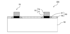
- the solar cell of the present invention includes a collector electrode 70 on the first main surface of the photoelectric conversion unit 50.
- the collector electrode 70 includes a first conductive layer 71 and a second conductive layer 72 in order from the photoelectric conversion unit 50 side.
- the solar cell of the present invention has an insulating layer 90 on at least a part of a region where the first conductive layer is not formed (first conductive layer non-formation region) on the first main surface of the photoelectric conversion unit.
- the insulating layer 90 includes a first insulating layer 91 that is in contact with the first conductive layer 71 and a second insulating layer 92 that is formed so as to cover at least part of the first insulating layer 91.
- heterojunction solar cell is a crystalline silicon solar cell in which a diffusion potential is formed by having a silicon thin film having a band gap different from that of single crystal silicon on the surface of a single crystal silicon substrate.
- the silicon-based thin film is preferably amorphous.
- a thin intrinsic amorphous silicon layer interposed between a conductive amorphous silicon thin film for forming a diffusion potential and a crystalline silicon substrate is a crystalline silicon solar cell having the highest conversion efficiency. It is known as one of the forms.
- FIG. 2 is a schematic cross-sectional view of a heterojunction solar cell according to an embodiment of the present invention.
- Heterojunction solar cell 105 has conductive silicon-based thin film 3a and light-receiving surface-side transparent electrode layer 6a in this order on first main surface (light-receiving surface) of single crystal silicon substrate 1 as photoelectric conversion unit 50.
- a conductive silicon thin film 3b and a back side transparent electrode layer 6b are provided in this order.
- a collector electrode 70 including a first conductive layer 71 and a second conductive layer 72 is formed on the light receiving surface side transparent electrode layer 6 a on the surface of the photoelectric conversion unit 50.
- intrinsic silicon thin films 2a and 2b between the single crystal silicon substrate 1 and the conductive silicon thin films 3a and 3b. It is preferable to have the back metal electrode 8 on the back side transparent electrode layer 6b.
- a single conductivity type single crystal silicon substrate used for a heterojunction solar cell contains an impurity that supplies electric charge to silicon in order to provide conductivity.
- Single crystal silicon substrates include an n-type in which atoms (for example, phosphorus) for introducing electrons into silicon atoms and a p-type in which atoms (for example, boron) for introducing holes into silicon atoms are contained. That is, “one conductivity type” in the present invention means either n-type or p-type.
- the heterojunction on the light receiving surface side is preferably a reverse junction.
- the single crystal silicon substrate 1 used for the heterojunction solar cell is preferably an n-type single crystal silicon substrate.
- the single crystal silicon substrate 1 preferably has a texture structure on the surface from the viewpoint of light confinement.
- a silicon-based thin film is formed on the surface of the single crystal silicon substrate on which the texture is formed.
- a method for forming a silicon-based thin film a plasma CVD method is preferable.
- conditions for forming a silicon thin film by plasma CVD a substrate temperature of 100 to 300 ° C., a pressure of 20 to 2600 Pa, and a high frequency power density of 0.004 to 0.8 W / cm 2 are preferably used.
- a source gas used for forming a silicon-based thin film a silicon-containing gas such as SiH 4 or Si 2 H 6 or a mixed gas of a silicon-based gas and H 2 is preferably used.
- the conductive silicon-based thin films 3a and 3b are one-conductive type or reverse-conductive type silicon-based thin films.
- the one conductivity type silicon-based thin film and the reverse conductivity type silicon-based thin film are n-type and p-type, respectively.
- B 2 H 6 or PH 3 is preferably used as the dopant gas for forming the p-type or n-type silicon-based thin film.
- the addition amount of impurities such as P and B may be small, it is preferable to use a mixed gas diluted with SiH 4 or H 2 in advance.
- a gas containing a different element such as CH 4 , CO 2 , NH 3 , GeH 4 is added to alloy the silicon thin film, thereby reducing the energy gap of the silicon thin film. It can also be changed.
- silicon thin films include amorphous silicon thin films, microcrystalline silicon (thin films containing amorphous silicon and crystalline silicon), and the like. Among these, it is preferable to use an amorphous silicon thin film.
- the transparent electrode layer 6a / p-type amorphous silicon thin film 3a / i type is used as a preferable configuration of the photoelectric conversion unit 50 when an n-type single crystal silicon substrate is used as the one-conductivity-type single crystal silicon substrate 1.
- Examples include a laminated structure in the order of amorphous silicon thin film 2a / n type single crystal silicon substrate 1 / i type amorphous silicon thin film 2b / n type amorphous silicon thin film 3b / transparent electrode layer 6b. In this case, it is preferable to use the p-layer side as the light-receiving surface for the reasons described above.
- i-type hydrogenated amorphous silicon composed of silicon and hydrogen is preferable.
- surface passivation can be effectively performed while suppressing impurity diffusion into the single crystal silicon substrate. Further, by changing the amount of hydrogen in the film, it is possible to give an effective profile to the carrier recovery in the energy gap.
- the p-type silicon thin film is preferably a p-type hydrogenated amorphous silicon layer, a p-type amorphous silicon carbide layer, or a p-type amorphous silicon oxide layer.
- a p-type hydrogenated amorphous silicon layer is preferable from the viewpoint of suppressing impurity diffusion and reducing the series resistance.
- the p-type amorphous silicon carbide layer and the p-type amorphous silicon oxide layer are wide gap low-refractive index layers, which are preferable in terms of reducing optical loss.
- the photoelectric conversion unit 50 of the heterojunction solar cell includes transparent electrode layers 6a and 6b on the conductive silicon thin films 3a and 3b.
- the transparent electrode layers 6a and 6b are mainly composed of a conductive oxide.
- the conductive oxide for example, zinc oxide, indium oxide, or tin oxide can be used alone or in combination. From the viewpoints of conductivity, optical characteristics, and long-term reliability, an indium oxide containing indium oxide is preferable, and an indium tin oxide (ITO) as a main component is more preferably used.
- the transparent electrode layer may be a single layer or a laminated structure composed of a plurality of layers.
- “having the main component” as a characteristic component means that the content is more than 50% by weight, preferably 70% by weight or more, and more preferably 90% by weight or more.
- a doping agent can be added to the transparent electrode layer.
- examples of the doping agent include aluminum, gallium, boron, silicon, and carbon.
- examples of the doping agent include zinc, tin, titanium, tungsten, molybdenum, and silicon.
- examples of the doping agent include fluorine.
- the doping agent can be added to one or both of the light-receiving surface side transparent electrode layer 6a and the back surface side transparent electrode layer 6b.
- a doping agent By adding a doping agent to the light-receiving surface side transparent electrode layer 6a, the resistance of the transparent electrode layer itself can be reduced, and loss due to resistance between the transparent electrode layer 6a and the collector electrode 70 can be suppressed. .
- the film thickness of the light-receiving surface side transparent electrode layer 6a is preferably 10 nm or more and 140 nm or less from the viewpoints of transparency, conductivity, and light reflection reduction.
- the role of the transparent electrode layer 6a is to transport carriers to the collector electrode 70, as long as it has conductivity necessary for that purpose, and the film thickness is preferably 10 nm or more.
- the film thickness of the transparent electrode layer 6a is within the above range, an increase in carrier concentration in the transparent electrode layer can also be prevented, so that a decrease in photoelectric conversion efficiency due to a decrease in transmittance in the infrared region is also suppressed.
- the method for forming the transparent electrode layer is not particularly limited, but a physical vapor deposition method such as a sputtering method, a chemical vapor deposition (MOCVD) method using a reaction between an organometallic compound and oxygen or water is preferable.
- a physical vapor deposition method such as a sputtering method, a chemical vapor deposition (MOCVD) method using a reaction between an organometallic compound and oxygen or water is preferable.
- MOCVD chemical vapor deposition
- energy by heat or plasma discharge can be used.
- the substrate temperature at the time of producing the transparent electrode layer is appropriately set.
- the temperature is preferably 200 ° C. or lower.
- the back surface metal electrode 8 is preferably formed on the back surface side transparent electrode layer 6b.
- the back surface metal electrode 8 it is desirable to use a material having high reflectivity from the near infrared to the infrared region and high conductivity and chemical stability. Examples of the material satisfying such characteristics include silver and aluminum.
- the method for forming the back surface metal electrode layer is not particularly limited, but a physical vapor deposition method such as a sputtering method or a vacuum evaporation method, a printing method such as screen printing, or the like is applicable.
- a collecting electrode 70 is formed on the light receiving surface side transparent electrode layer 6a.
- the collector electrode 70 includes a first conductive layer 71 and a second conductive layer 72 from the photoelectric conversion unit 50 side.
- the second conductive layer 72 is formed by a plating method.
- the first conductive layer 71 is a layer that functions as a conductive underlayer when the second conductive layer is formed by a plating method. Therefore, the first conductive layer only needs to have conductivity that can function as a base layer for electrolytic plating. Note that in this specification, a volume resistivity of 10 ⁇ 2 ⁇ ⁇ cm or less is defined as conductive. Further, if the volume resistivity is 10 2 ⁇ ⁇ cm or more, it is defined as insulating.
- the first conductive layer 71 can be produced by a known technique such as an inkjet method, a screen printing method, a conductive wire bonding method, a spray method, a vacuum deposition method, or a sputtering method.
- the first conductive layer 71 is preferably patterned in a predetermined shape such as a comb shape.
- a screen printing method is suitable for forming the patterned first conductive layer from the viewpoint of productivity.
- the collector electrode pattern is printed using a conductive printing paste and a screen plate having an opening pattern corresponding to the pattern shape of the collector electrode.
- the first conductive layer 71 is preferably formed using a conductive paste containing conductive fine particles and an insulating material.
- a conductive paste containing conductive fine particles and an insulating material As the insulating material, a binder resin or the like can be used. In particular, as will be described later, when the first insulating layer is formed by oozing out the insulating material contained in the first conductive layer forming material, it is preferable to use a binder resin as the insulating material.
- thermosetting resin such as an epoxy resin, a phenol resin, or an acrylic resin is preferably used. These resins may be solid resins or liquid resins.
- the conductive paste may contain an organic solvent or an inorganic solvent. By including a liquid material such as a liquid resin or an organic solvent in the conductive paste, applicability (printability) can be improved.
- the conductive fine particles a single metal material such as silver, aluminum, copper, indium, bismuth, gallium, or a plurality of metal materials can be used.
- the particle diameter of the conductive fine particles 710 is preferably 0.25 ⁇ m or more, and more preferably 0.5 ⁇ m or more.
- the particle diameter of the conductive fine particles can be appropriately set according to the mesh size of the screen plate.
- the particle size is preferably smaller than the mesh size, and more preferably 1 ⁇ 2 or less of the mesh size.
- the particle size is defined by the diameter of a circle having the same area as the projected area of the particles (projected area circle equivalent diameter, Heywood diameter).
- the first conductive layer is formed by curing a conductive paste containing conductive fine particles and an insulating material.
- the drying temperature is preferably 250 ° C. or less, more preferably 200 ° C. or less, more preferably 180 ° C. in consideration of the heat resistance of the transparent electrode layer of the photoelectric conversion part or the amorphous silicon thin film. More preferably, it is as follows.
- the drying time can be appropriately set, for example, from about 5 minutes to 1 hour.
- the film thickness of the first conductive layer 71 is preferably 20 ⁇ m or less, more preferably 10 ⁇ m or less from the viewpoint of cost. On the other hand, from the viewpoint of setting the line resistance of the first conductive layer 71 in a desired range, the thickness of the first conductive layer 71 is preferably 0.5 ⁇ m or more, and more preferably 1 ⁇ m or more.
- the first conductive layer 71 may be composed of a plurality of layers.
- a laminated structure including a lower layer having a low contact resistance with the transparent electrode layer on the surface of the photoelectric conversion portion and an upper layer containing a material having a high binder resin content may be used. According to such a structure, an improvement in the curve factor of the solar cell can be expected with a decrease in contact resistance with the transparent electrode layer.
- the above description has focused on the case where the first conductive layer is formed by screen printing.
- the method for forming the first conductive layer is not limited to the printing method, and a pattern may be formed by an inkjet method or the like.
- a second conductive layer 72 is formed on the first conductive layer 71 by a plating method.
- the metal deposited as the second conductive layer is not particularly limited as long as it is a material that can be formed by a plating method. For example, copper, nickel, tin, aluminum, chromium, silver, gold, zinc, lead, palladium, etc., or these Mixtures can be used.
- the line resistance of the second conductive layer is preferably as small as possible.
- the line resistance of the second conductive layer is preferably 1 ⁇ / cm or less, and more preferably 0.5 ⁇ / cm or less.
- the line resistance of the first conductive layer only needs to be small enough to function as a base layer during electrolytic plating, and may be 5 ⁇ / cm or less.
- the second conductive layer can be formed by either an electroless plating method or an electrolytic plating method. From the viewpoint of productivity, the electrolytic plating method is preferable. In the electroplating method, since the metal deposition rate can be increased, the second conductive layer can be formed in a short time.
- FIG. 3 is a conceptual diagram of the plating apparatus 10 used for forming the second conductive layer.
- a substrate 12 having a first conductive layer formed on the photoelectric conversion portion and an anode 13 are immersed in a plating solution 16 in the plating tank 11.
- the first conductive layer 71 on the substrate 12 is connected to the power source 15 via the substrate holder 14.
- copper can be deposited on the first conductive layer.
- the plating solution 16 used for acidic copper plating contains copper ions.
- a known composition mainly composed of copper sulfate, sulfuric acid, and water can be used, and a metal layer is deposited as the second conductive layer by applying a current of 0.1 to 10 A / dm 2 to the composition. be able to.
- An appropriate plating time is appropriately set according to the area of the collecting electrode, current density, cathode current efficiency, set film thickness, and the like.
- the second conductive layer may be composed of a plurality of layers. For example, after a first plating layer made of a material having high conductivity such as Cu is formed on the first conductive layer through the opening of the insulating layer, the second plating layer having excellent chemical stability is formed on the first plating layer. By forming on the surface of one plating layer, a collector electrode having low resistance and excellent chemical stability can be formed.
- the second conductive layer is formed on the first conductive layer by plating. If the region where the first conductive layer on the photoelectric conversion part is not formed (the first conductive layer non-formation region) is exposed at the time of forming the second conductive layer, the photoelectric conversion unit comes into contact with the plating solution, and the photoelectric conversion unit Metal ions in the plating solution enter the conversion part (silicon substrate or the like), resulting in deterioration of solar cell characteristics.
- the transparent electrode layer is energized during the electrolytic plating. Therefore, metal is deposited also in the first conductive layer non-formation region.
- the insulating layer 90 is formed in the first conductive layer non-forming region of the photoelectric conversion part, and after the formation of the insulating layer, the second conductive layer is formed by plating.
- the insulating layer 90 includes a first insulating layer 91 that is in contact with the first conductive layer 71 and a second insulating layer 92 that is formed so as to cover at least part of the first insulating layer 91.
- FIG. 4 is a process conceptual diagram showing a method of forming the insulating layer 90 and the collecting electrode 70 on the photoelectric conversion unit 50 of the solar cell according to the first embodiment of the present invention.
- the photoelectric conversion unit 50 is prepared (photoelectric conversion unit preparation step, FIG. 4A).
- photoelectric conversion unit preparation step FIG. 4A.
- a photoelectric conversion unit including a silicon-based thin film and a transparent electrode layer is prepared on a silicon substrate.
- a conductive paste including the conductive fine particles 710 and the insulating material 712 is applied.
- the conductive paste is applied (printed) using a screen plate having an opening pattern corresponding to the shape of the collector electrode.
- a conductive paste application region 80 having a width substantially equal to W 0 is formed on the photoelectric conversion portion (FIG. 4B )).
- the ratio between the insulating material and the conductive fine particles in the conductive paste is set to be equal to or higher than a so-called percolation threshold (a critical value of the ratio corresponding to the content of conductive fine particles exhibiting conductivity).
- a paste is spread wetting the surface of the photoelectric conversion unit, the larger the coating layer 81 in the width than the opening width W 0 of the screen plate (FIG. 4 (C) ).
- the insulating material in the paste oozes out from the coating region and wets and spreads on the photoelectric conversion portion, thereby contacting the outer edge of the first conductive layer 71 including the conductive fine particles 710 and the insulating material 712, A first insulating layer 91 is formed.
- the first insulating layer 91 is formed of the same material as the insulating material in the first conductive layer 71.
- the binder resin oozes out from the coating region and contacts the outer edge of the first conductive layer.
- An insulating layer is formed.
- the width L 9 from the boundary 7B where the first conductive layer 71 and the first insulating layer 91 are in contact to the end 9B of the first insulating layer, that is, the line width of the first insulating layer is preferably 0.2 mm to 1.0 mm. 0.5 mm to 1.0 mm is more preferable.
- the 1st insulating layer 91 is formed when an insulating material (binder resin) oozes out from the electrically conductive paste for 1st conductive layer formation, as shown in FIG. In the parallel direction, the plurality of conductive fine particles 710 are in contact with each other, the electrically conductive region is the first conductive layer 71, and the region in contact with the outer edge of the first conductive layer 71 is the first insulating layer 91. It is. Even when a part of the conductive fine particles in the conductive paste oozes out together with the insulating material, the conductive fine particles 710 of the first conductive layer 71 and the conductive fine particles 710 and 719 in FIG.
- an insulating material binder resin
- the region including these isolated conductive fine particles is regarded as the first insulating layer.
- the conductive fine particles “not electrically conductive” typically means that the conductive fine particles in the exuded portion are covered with an insulating material and are isolated from other conductive fine particles. Means. From the viewpoint of suppressing light shielding by the conductive fine particles, the first insulating layer 91 preferably contains few conductive fine particles, and the first insulating layer more preferably does not contain conductive fine particles.
- the line width of the first insulating layer 91 is set to a desired value. It can be a range. From the viewpoint of suppressing the seepage of the conductive fine particles to the first insulating layer, the particle diameter of the conductive fine particles is preferably 0.25 ⁇ m or more, and more preferably 0.5 ⁇ m or more. The particle diameter of the conductive fine particles is more preferably 2 to 3 ⁇ m.
- the conductive paste has a viscosity at 25 ° C.
- the content of the insulating resin material in the conductive paste is preferably adjusted so that the viscosity of the paste falls within the above range.
- the optimum value of the content varies depending on the type of resin, but is preferably 5 wt% to 20 wt%, for example.
- the conductive paste contains a solvent, drying is performed as necessary.
- the conductive paste may be cured by light irradiation or heating.
- the second insulating layer 92 is formed on the first conductive layer non-formation region. Is formed (second insulating layer forming step).
- the second insulating layer 92 is formed so as to cover at least a part of the first insulating layer 91 (FIG. 4D).
- the second insulating layer 92 is preferably formed so as to cover the entire surface of the first insulating layer 91.
- the second insulating layer 92 may also be formed on the first conductive layer 71.
- the second insulating layer is not formed in at least a part of the first conductive layer formation region. That is, the second insulating layer 92 has an opening 92h on the first conductive layer formation region.
- film formation is performed so that the second insulating layer is not formed in at least a part of the first conductive layer forming region.
- the method for forming the second insulating layer include dry methods such as CVD, sputtering, and vapor deposition, and wet methods such as screen printing, inkjet, and spray coating.
- film formation is performed in a state where the first conductive layer 71 is covered with the mask 95 so that the second insulating layer is not formed on the first conductive layer.
- the opening 92h can be formed on the first conductive layer formation region.
- the second insulating layer is formed by screen printing
- insulation is performed using a screen plate having an opening pattern corresponding to the pattern (negative electrode pattern) opposite to the shape of the first conductive layer forming region (that is, the shape of the collector electrode).
- Application (printing) of the functional material is performed.
- the second insulating layer 92 is formed so as to cover at least a part of the first insulating layer 91.
- the second insulating layer 92 is preferably formed on the entire surface of the region where the coating layer 81 is not formed. Thereby, the entire surface of the first conductive layer non-formation region on the first main surface is covered with the insulating layer 90. That is, it is preferable that the first conductive layer non-formation region on the first main surface is covered with at least one of the first insulating layer 91 and the second insulating layer 92.
- the second conductive layer 72 is formed by a plating method (plating step, FIG. 4E).
- the first conductive layer 71 is exposed in the opening 92h where the second insulating layer 92 is not formed. Therefore, in the plating step, the first conductive layer is exposed to the plating solution, and metal can be deposited starting from the opening 92h.
- the insulating layer 90 is formed on the entire surface of the first conductive layer non-formation region, when the second conductive layer is formed by the plating method, the insulating layer 90 becomes a protective layer, and the photoelectric conversion unit 50 is replaced with the plating solution. It can be chemically and electrically protected.
- the transparent electrode layer 6a is formed on the surface of the photoelectric conversion unit 50 as in a heterojunction solar cell, the transparent electrode layer and the plating solution are formed by forming the insulating layer 90 on the surface of the transparent electrode layer. Can be prevented and dissolution of the transparent electrode layer and precipitation of the metal layer (second conductive layer) on the transparent electrode layer can be prevented.
- the collector electrode on the light-receiving surface side of the solar cell is required to have a small line width (small light-shielding area) and low resistance, it is preferable that the ratio of thickness to width (aspect ratio) is large.
- Patent Document 3 Japanese Patent Laid-Open No. 2010-98232
- the line width of the collector electrode increases, and the aspect ratio decreases.
- the light shielding area is increased. Therefore, when a collector electrode or a conductive seed is formed using a conductive paste, a conductive paste having a high viscosity and hardly exuding due to wetting and spreading is generally used.
- the conductive paste is wet spread on the photoelectric conversion part and the insulating material oozes out, whereby the first conductive layer 71 and the first insulating layer 91 in contact with the outer edge thereof are It is formed as a continuous integral coating layer 81. Therefore, when no gap is formed between the first conductive layer and the insulating layer, and there are pinholes or locally small portions in the second insulating layer formed on the first insulating layer However, the contact between the photoelectric conversion part in the vicinity of the first conductive layer and the plating solution is suppressed, and the first conductive layer is hardly peeled off from the photoelectric conversion part.
- the insulating layer 90 since the second insulating layer 92 is formed on the first insulating layer 91 in contact with the outer edge of the first conductive layer 71, the insulating layer 90 has two layers in the vicinity of the first conductive layer 71. It becomes composition.
- the first conductive layer forming region and the surface of the photoelectric conversion unit in the vicinity thereof are contact regions between the photoelectric conversion unit and the collector electrode. Since the insulating layer 90 on the contact region has a two-layer structure, the contact between the plating solution and the contact region of the photoelectric conversion portion is greatly reduced in the plating step.
- the first insulating layer 91 since the first insulating layer 91 is formed in contact with the outer edge of the first conductive layer 71, at the time of forming the second insulating layer, it covers at least a part of the first conductive layer forming region.
- a mask may be disposed at a position, and a margin of alignment accuracy corresponding to the width L 9 of the first insulating layer 91 exists. Therefore, when forming the second insulating layer, it is not necessary to strictly align the mask and the printing position, and the productivity can be improved.
- the second insulating layer 92 is desirably a material having chemical stability with respect to the plating solution.
- the second insulating layer 92 is desirably a material having chemical stability with respect to the plating solution.
- the second insulating layer 92 preferably has a high adhesion strength with the photoelectric conversion unit 50.
- the second insulating layer 92 has a high adhesion strength with the light receiving surface side transparent electrode layer 6a on the surface of the photoelectric conversion unit 50.
- the second insulating layer 92 is formed on the light receiving surface side of the photoelectric conversion unit 50, more light can be taken into the photoelectric conversion unit if light absorption by the insulating layer is small.
- the second insulating layer 92 has sufficient transparency with a transmittance of 90% or more, optical loss due to light absorption in the second insulating layer is small, and the insulating layer is removed after forming the second conductive layer. It can be used as it is as a solar cell. Therefore, the manufacturing process of a solar cell can be simplified and the productivity of the solar cell can be further improved.
- the second insulating layer 92 is made of a material having sufficient weather resistance and stability against heat and humidity in addition to transparency. It is more desirable to be formed.
- the material of the second insulating layer may be an inorganic insulating material or an organic insulating material.
- the inorganic insulating material for example, materials such as silicon oxide, silicon nitride, titanium oxide, aluminum oxide, magnesium oxide, and zinc oxide can be used.
- the organic insulating material for example, materials such as polyester, ethylene vinyl acetate copolymer, acrylic, epoxy, polyurethane, and organic siloxane can be used.
- An organic-inorganic hybrid insulating material can also be used.
- an insulating layer made of an inorganic material such as silicon oxide or silicon nitride a dry method such as a plasma CVD method or a sputtering method is preferably used.
- the film thickness is in the range of 30 nm to 250 nm from the viewpoint of imparting suitable antireflection characteristics to the second insulating layer 92. Is preferably set within the range of 50 nm to 250 nm.
- a wet method such as a screen printing method is preferably used. According to these methods, it is possible to form a dense film with few defects such as pinholes.
- the film thickness of the second insulating layer 92 is appropriately set according to the material and forming method of the second insulating layer.
- the second insulating layer 92 is preferably thick enough to completely cover the surface irregularities of the transparent conductive layer during the insulating layer printing.
- the film thickness of the second insulating layer is preferably 10 ⁇ m or more, and more preferably 15 ⁇ m or more.
- the thickness of the second insulating layer is preferably 40 ⁇ m or less, and more preferably 30 ⁇ m or less.
- the second insulating layer having the opening 92h on the first conductive layer formation region by a method of coating the first conductive layer using a mask or the like, a printing method, or the like. 92 is formed.
- the second embodiment of the present invention after the second insulating layer 92 is formed on the entire surface of the first conductive layer 71, an opening is formed in the second insulating layer 92 on the first conductive layer 71, The second conductive layer 72 is formed by plating using this opening as a starting point.
- the method for forming the opening in the second insulating layer is not particularly limited, and the insulating layer is locally peeled off by using sanding, mechanical drilling, adhesive tape, or the like. Methods, laser irradiation, chemical etching, etc. can be employed.
- an opening is formed in the second insulating layer on the first conductive layer by thermally flowing the low melting point material in the first conductive layer.
- the surface shape of the first conductive layer is changed by heating (annealing) the heat flow starting temperature T 1 or higher of the low melting point material.
- an opening (crack) is formed in the second insulating layer formed thereon.
- FIG. 6 is a process conceptual diagram showing a method of forming the insulating layer 90 and the collecting electrode 70 on the photoelectric conversion unit 50 of the solar cell according to the second embodiment of the present invention.
- the photoelectric conversion unit 50 is prepared (photoelectric conversion unit preparation step, FIG. 6A).
- a conductive paste including a low-melting-point material 711 and an insulating material 712 is applied on the first main surface of the photoelectric conversion unit 50 to form a first conductive layer (FIG. 6B).
- the low melting point material 711 is preferably conductive fine particles.
- the conductive paste contains a low melting point material 711 and an insulating material (resin material) 712.
- the conductive paste contains a conductive material in addition to the low melting point material and the resin material.
- the conductive paste may contain another material such as the high melting point material 713 in addition to the low melting point material 711.
- the insulating material in the paste oozes out from the conductive paste application region 83 and spreads on the photoelectric conversion portion, so that the outer edge of the first conductive layer 71 is obtained.
- a first insulating layer 91 is formed in contact with (FIG. 6C).
- the second insulating layer 92 is formed on the first conductive layer non-formation region. Is formed (second insulating layer forming step).
- the second insulating layer 92 is formed so as to cover substantially the entire coating layer 84, that is, substantially the entire first conductive layer 71 and the first insulating layer 91 (FIG. 6D).
- substantially covering the entire case means that in addition to the case where the entire first conductive layer and the first insulating layer are covered, there are local pinholes or the insulating layer is locally island-shaped. Including the state of being formed.
- the second insulating layer 92 is formed on the entire surface of the region where the coating layer 84 is not formed, and the entire surface of the first conductive layer non-forming region on the first main surface is covered with the insulating layer 90. It is preferable.
- an annealing process by heating is performed (annealing process, FIG. 6E).
- the first conductive layer 71 is heated to the annealing temperature Ta, and the low melting point material 711 is thermally fluidized, whereby the surface shape of the first conductive layer 71 changes.
- the second insulating layer 92 formed on the first conductive layer 71 is deformed, and the opening 90h is formed.
- the opening is formed in a crack shape, for example.
- the second conductive layer 72 is formed by a plating method (plating step, FIG. 6 (F)).
- plating step FIG. 6 (F)
- the first conductive layer 71 is covered with the second insulating layer 92, the first conductive layer 71 is exposed in the opening 90 h of the second insulating layer 92. Therefore, the first conductive layer is exposed to the plating solution in the plating step, and metal can be deposited starting from the opening 90h.
- the insulating layer 90 has a two-layer structure in the vicinity of the first conductive layer 71, the contact between the photoelectric conversion portion and the plating solution can be prevented in the plating step.
- the second insulating layer may be formed on the entire surface, it is not necessary to align the mask or the screen plate in the vicinity of the collector electrode formation region when forming the second insulating layer, thereby improving productivity. be able to.
- the first conductive layer 71 includes a low melting point material 711 of the heat flow temperature T 1.
- the softening point is a temperature at which the viscosity becomes 4.5 ⁇ 10 6 Pa ⁇ s (the same as the definition of the softening point of glass).
- the low melting point material is preferably a material that causes heat flow in the annealing process and changes the surface shape of the first conductive layer 71. Therefore, the thermal flow temperature T 1 of the low-melting material is preferred over heating temperature (annealing temperature) Ta in the annealing step is cold.
- the lower limit of the thermal flow temperature T 1 of the low melting point material is not particularly limited.
- the low-melting-point material is thermally fluidized during the formation of the first conductive layer. It is preferable not to produce.
- the first conductive layer 71 (and the first insulating layer 91) is formed using a conductive paste, heating may be performed to dry the paste.
- the heat flow temperature T 1 of the low melting point materials is preferably higher than the heating temperature for drying the conductive paste. From this viewpoint, the heat flow temperature T 1 of the low melting point materials is preferably at least 80 ° C., more preferably at least 100 ° C..
- Low melting point material if the heat flow temperature T 1 is the above-mentioned range, be organic, it may be inorganic.
- the low melting point material may be electrically conductive or insulating, but is preferably a metal material having conductivity. If the low-melting-point material is a metal material, the resistance value of the first conductive layer can be reduced. Therefore, when the second conductive layer is formed by electroplating, the film thickness of the second conductive layer is increased. Can do. In addition, when the low melting point material is a metal material, the contact resistance between the photoelectric conversion unit 50 and the collector electrode 70 can be reduced.
- the conductive low melting point material a simple substance or an alloy of a low melting point metal material or a mixture of a plurality of low melting point metal materials can be suitably used.
- the low melting point metal material include indium, bismuth, and gallium.
- Low melting point material if a particulate material such as fine metal particles, from the viewpoint of facilitating formation of the opening to the second insulating layer by the annealing process, the particle size D L of the low-melting material, the first conductive layer 71
- the film thickness is preferably 1/20 or more, more preferably 1/10 or more.
- the shape of the particles of the low melting point material is not particularly limited, but a non-spherical shape such as a flat shape is preferable. In addition, non-spherical particles obtained by combining spherical particles by a technique such as sintering are also preferably used. Generally, when the metal particles are in a liquid phase, the surface shape tends to be spherical in order to reduce the surface energy. If low melting point material of the first conductive layer before annealing is non-spherical, the annealing is heated in heat flow starting temperature above T 1, since the particles approaches the spherical shape, the surface shape of the first conductive layer The amount of change is greater. Therefore, it is easy to form an opening in the second insulating layer 92 on the first conductive layer 71.
- the first conductive layer 71 preferably contains a high melting point material having a heat flow starting temperature relatively higher than that of the low melting point material in addition to the above low melting point material. Since the first conductive layer 71 includes the high melting point material 713, the first conductive layer and the second conductive layer can be efficiently conducted, and the conversion efficiency of the solar cell can be improved. For example, when a material having a large surface energy is used as the low melting point material, when the first conductive layer 71 is exposed to a high temperature by the annealing process and the low melting point material is in a liquid phase, particles of the low melting point material gather. In some cases, the first conductive layer 71 may be disconnected due to coarse particles.
- the first conductive layer forming material contains the high melting point material, so that the first conductive layer is coarsened by the low melting point material. The disconnection of the layer can be suppressed.
- Heat flow temperature T 2 of the high-melting material is preferably higher than the annealing temperature Ta. That is, when the first conductive layer 71 contains a low melting point material and a high melting point material, the heat flow starting temperature T 1 of the low melting point material, the heat flow starting temperature T 2 of the high melting point material, and the annealing temperature Ta in the annealing process are: , T 1 ⁇ Ta ⁇ T 2 is preferably satisfied.
- the high melting point material may be an insulating material or a conductive material, but a conductive material is preferable from the viewpoint of reducing the resistance of the first conductive layer.
- the resistance of the first conductive layer as a whole can be reduced by using a material having high conductivity as the high melting point material.
- a material having high conductivity for example, a single metal material such as silver, aluminum, copper, or a plurality of metal materials can be preferably used.
- the content ratio is to suppress disconnection due to coarsening of the low-melting-point material as described above, to the conductivity of the first conductive layer, to the insulating layer. From the standpoint of easiness of forming the opening (increase in the number of starting points of metal deposition of the second conductive layer), etc., it is appropriately adjusted. The optimum value differs depending on the material used and the combination of particle sizes.
- the weight ratio of the low melting point material to the high melting point material (low melting point material: high melting point material) is 5:95 to 67:33. It is a range.
- the weight ratio of the low melting point material to the high melting point material is more preferably 10:90 to 50:50, and further preferably 15:85 to 35:65.
- the first conductive layer 71 may be conductive and have a volume resistivity of 10 ⁇ 2 ⁇ ⁇ cm or less.
- the volume resistivity of the first conductive layer 71 is preferably 10 ⁇ 4 ⁇ ⁇ cm or less.
- the low melting point material only needs to have conductivity.
- the combination of low melting point material / high melting point material includes insulation / conductivity, conductivity / insulation, conductivity / conductivity.
- Both the low melting point material and the high melting point material are preferably conductive materials.
- the opening 90 h of the second insulating layer 92 is mainly formed on the low melting point material 711 of the first conductive layer 71.
- the low-melting point material is an insulating material, it is insulative immediately below the opening.
- the plating solution penetrates into the conductive high-melting point material around the low-melting point material, the first conductive layer and the plating layer are plated. It is possible to conduct the liquid.
- the heating at the annealing process is performed. It is also possible to improve the conversion efficiency by suppressing disconnection of the first conductive layer. For example, if a material having a high melting point such as silver, copper, gold or the like is fine particles having a particle size of 1 ⁇ m or less, sintering necking (particulate particles) at a temperature T 1 ′ of about 200 ° C. or lower than the melting point Therefore, it can be used as the “low melting point material” of the present invention.
- a material having a high melting point such as silver, copper, gold or the like is fine particles having a particle size of 1 ⁇ m or less, sintering necking (particulate particles) at a temperature T 1 ′ of about 200 ° C. or lower than the melting point Therefore, it can be used as the “low melting point material” of the present invention.
- a material that causes sintering necking such as metal fine particles is a “low melting point material” in the present invention but also has a side surface as a “high melting point material”.
- sintering necking start temperature T 1 ′ heat flow start temperature T 1 .
- the film thickness of the second insulating layer 92 is thin enough that an opening can be formed in the second insulating layer due to interface stress or the like that occurs due to a change in the surface shape of the first conductive layer in the annealing process. It is preferable. From this viewpoint, the film thickness of the second insulating layer 92 is preferably 1000 nm or less, and more preferably 500 nm or less. Note that the film thickness of the second insulating layer on the first conductive layer forming region and the film thickness of the second insulating layer on the first conductive layer non-forming region may be different.
- the thickness of the second insulating layer is set from the viewpoint of facilitating the formation of the opening by annealing, and in the first conductive layer non-formation region, an optical having appropriate antireflection characteristics.
- the film thickness of the second insulating layer may be set to be a film thickness.
- the material of the second insulating layer may be an inorganic insulating material or an organic insulating material.
- the material of the insulating layer is elongation at break. Is preferably an inorganic material.
- the second insulating layer 92 on the first conductive layer formation region does not necessarily have to be a continuous layer shape, and may have an island shape.
- island shape in this specification means a state in which a part of the surface has a region where an insulating layer is not formed.
- the second insulating layer 92 on the first conductive layer formation region can also contribute to an improvement in the adhesion between the first conductive layer 71 and the second conductive layer 72.
- the adhesion between the Ag layer and the Cu layer is small, but the Cu layer is formed on the second insulating layer made of silicon oxide or the like. As a result, it is expected that the adhesion of the second conductive layer is enhanced and the reliability of the solar cell is improved.
- the annealing temperature (heating temperature) Ta during the annealing treatment is preferably higher than the thermal flow start temperature T 1 of the low melting point material, that is, T 1 ⁇ Ta.
- the annealing temperature Ta preferably satisfies T 1 + 1 ° C. ⁇ Ta ⁇ T 1 + 100 ° C., and more preferably satisfies T 1 + 5 ° C. ⁇ Ta ⁇ T 1 + 60 ° C.
- the annealing temperature can be appropriately set according to the composition and content of the material of the first conductive layer.
- the annealing temperature Ta is preferably lower than the heat resistant temperature of the photoelectric conversion unit 50.
- the heat flow start temperature T 1 of the low melting point material of the first conductive layer 71 is also preferably lower than the heat resistant temperature of the photoelectric conversion part.
- the heat-resistant temperature of the photoelectric conversion unit is a temperature at which the characteristics of a solar cell provided with the photoelectric conversion unit or a solar cell module manufactured using the solar cell irreversibly decreases, and varies depending on the configuration of the photoelectric conversion unit.
- a crystalline silicon substrate constituting a photoelectric conversion part hardly changes in characteristics even when heated to a high temperature of 500 ° C. or higher, but a transparent electrode layer or an amorphous silicon thin film is 250 ° C. When heated to such a degree, thermal deterioration may occur or diffusion of doped impurities may occur, resulting in an irreversible decrease in solar cell characteristics.
- the heat-resistant temperature in the case of having a transparent electrode layer or an amorphous silicon thin film like a heterojunction solar cell or a silicon thin film solar cell is about 250 ° C. Therefore, in the case of a heterojunction solar cell in which the photoelectric conversion portion includes an amorphous silicon thin film or a silicon thin film solar cell, the annealing temperature is 250 from the viewpoint of suppressing thermal damage at the amorphous silicon thin film and its interface. It is preferable that the temperature is set to be equal to or lower. In order to realize a higher performance solar cell, the annealing temperature is more preferably 200 ° C. or lower, and further preferably 180 ° C. or lower.
- the crystalline silicon solar cell having the reverse conductivity type diffusion layer on the first main surface of the one conductivity type crystal silicon substrate does not have an amorphous silicon thin film or a transparent electrode layer.
- the annealing process may be performed at an annealing temperature Ta higher than 250 ° C.
- the method of forming the opening in the second insulating layer is not limited to the method of performing the annealing process after forming the insulating layer.
- the opening can be formed substantially simultaneously with the formation of the insulating layer by forming the second insulating layer while heating the substrate.
- substantially simultaneously with the formation of the insulating layer means that a separate step such as annealing is not performed in addition to the insulating layer forming step, that is, during or immediately after the formation of the insulating layer. Means the state.
- the term “immediately after film formation” includes the period from the end of film formation of the insulating layer (after the stop of heating) to the time when the substrate is cooled and returned to room temperature or the like.
- the insulating layer on the low-melting-point material when an opening is formed in the insulating layer on the low-melting-point material, even after the insulating layer on the low-melting-point material has been formed, the insulating layer is formed around the periphery. Thus, the case where the insulating layer around the low melting point material is deformed and an opening is formed is included.
- the substrate is heated to a temperature Tb higher than the thermal flow start temperature T 1 of the low melting point material 711 of the first conductive layer 71.
- a method of forming the second insulating layer 92 on the first conductive layer 71 is used. Since the second insulating layer 92 is formed on the first conductive layer in which the low melting point material is in a fluid state, stress is generated at the film forming interface simultaneously with the film formation, for example, a crack-shaped opening is formed in the insulating layer. It is formed.
- the substrate temperature Tb at the time of forming the insulating layer represents the substrate surface temperature (also referred to as “substrate heating temperature”) at the start of the formation of the insulating layer.
- the average value of the substrate surface temperature during the formation of the insulating layer is usually equal to or higher than the substrate surface temperature at the start of film formation. Therefore, the insulating layer forming temperature Tb, if elevated temperatures than the heat flow temperature T 1 of the low melting point material, it is possible to form the deformation of openings such as the insulating layer.
- the substrate surface temperature in the insulating layer deposition is set to be higher than the thermal flow start temperature T 1 of the low melting point material.
- an opening can be formed.
- the second insulating layer 92 is formed by a wet method
- the opening is formed by setting the substrate surface temperature when drying the solvent to be higher than the thermal flow start temperature T 1 of the low melting point material.
- the “film formation start point” when the insulating layer is formed by a wet method refers to the time point when the solvent starts drying.
- the preferable range of the insulating layer formation temperature Tb is the same as the preferable range of the annealing temperature Ta.
- the substrate surface temperature can be measured, for example, by attaching a temperature display material (also called a thermo label or thermo seal) or a thermocouple to the substrate surface.
- a temperature display material also called a thermo label or thermo seal
- a thermocouple to the substrate surface.
- the temperature of the heating unit (such as a heater) can be appropriately adjusted so that the surface temperature of the substrate falls within a predetermined range.
- the above-described annealing step may be further performed.
- the second conductive layer is formed by plating starting from the opening (part) of the insulating layer on the first conductive layer.
- the plating solution remaining on the surface of the substrate 12 is preferably removed.
- the metal deposited in the first conductive layer non-formation region can be removed. Examples of the metal deposited in the first conductive layer non-formation region include those starting from pinholes of the second insulating layer 92 and the like. By removing such a metal in the plating solution removing step, light shielding is reduced and the solar cell characteristics can be further improved.
- the insulating layer on the photoelectric conversion portion may be removed after the collector electrode is formed (after the plating step).
- the second insulating layer when a material having high light absorption is used as the second insulating layer, it is preferable to perform an insulating layer removing step in order to suppress deterioration of solar cell characteristics due to light absorption of the insulating layer.
- the method for removing the second insulating layer is appropriately selected according to the characteristics of the insulating layer material.
- the second insulating layer can be removed by chemical etching or mechanical polishing. An ashing method can also be applied depending on the material.
- the second insulating layer on the first conductive layer non-forming region is removed from the viewpoint of further improving the light capturing effect.
- the insulating layer removing step does not need to be performed.
- the collector electrode 70 is provided on the light receiving surface side of the heterojunction solar cell, but a similar collector electrode may be formed on the back surface side. Since a solar cell using a crystalline silicon substrate, such as a heterojunction solar cell, has a large amount of current, in general, power generation loss due to contact resistance between the transparent electrode layer and the collector electrode tends to be significant. On the other hand, since the collector electrode having the first conductive layer and the second conductive layer has a low contact resistance with the transparent electrode layer, according to the present invention, it is possible to reduce power generation loss due to the contact resistance. It becomes.
- the present invention provides a crystalline silicon solar cell other than a heterojunction solar cell, a solar cell using a semiconductor substrate other than silicon such as GaAs, a pin junction or a pn junction of an amorphous silicon thin film or a crystalline silicon thin film.
- Various solar cells such as silicon-based thin-film solar cells with transparent electrode layers, compound semiconductor solar cells such as CIS and CIGS, organic thin-film solar cells such as dye-sensitized solar cells and organic thin films (conductive polymers) It is applicable to.
- the crystalline silicon solar cell has a reverse conductivity type (for example, n-type) diffusion layer on the first main surface of one conductivity type (for example, p-type) crystal silicon substrate, and the collector electrode on the diffusion layer. Is mentioned.
- a crystalline silicon solar cell is generally provided with a conductive layer such as a p + layer on the back side of one conductive layer.
- heat flow temperature T 1 and the annealing temperature Ta of the low melting point material may be higher than 250 ° C..
- the silicon thin film solar cell examples include an amorphous silicon thin film solar cell having an amorphous intrinsic (i type) silicon thin film between a p type thin film and an n type thin film, and a p type thin film and an n type thin film.
- Examples thereof include a crystalline silicon-based semiconductor solar cell having a crystalline intrinsic silicon thin film between the thin film.
- a tandem thin film solar cell in which a plurality of pin junctions are stacked is also suitable.
- the thermal flow temperature T 1 and the annealing temperature Ta of the low melting point material is 250 ° C. or less
- it is 200 degrees C or less, More preferably, it is 180 degrees C or less.
- the solar cell of the present invention is preferably modularized for practical use.
- the modularization of the solar cell is performed by an appropriate method.
- a bus bar is connected to the collector electrode via an interconnector such as a tab, so that a plurality of solar cells are connected in series or in parallel, and sealed by a sealing material and a glass plate, thereby being modularized. Done.
- the etched wafer was introduced into the CVD apparatus, and an i-type amorphous silicon film having a thickness of 5 nm was formed on the light receiving surface side as the intrinsic silicon-based thin film 2a.
- the film formation conditions for the i-type amorphous silicon were: substrate temperature: 150 ° C., pressure: 120 Pa, SiH 4 / H 2 flow rate ratio: 3/10, and input power density: 0.011 W / cm 2 .
- the film thickness of the thin film in this production example is measured by spectroscopic ellipsometry (trade name M2000, manufactured by JA Woollam Co., Ltd.) on the glass substrate under the same conditions. It is a value calculated from the film forming speed obtained by this.
- a p-type amorphous silicon film having a thickness of 7 nm was formed as the reverse conductivity type silicon-based thin film 3a.
- the film forming conditions for the p-type amorphous silicon layer 3a were as follows: the substrate temperature was 150 ° C., the pressure was 60 Pa, the SiH 4 / B 2 H 6 flow rate ratio was 1/3, and the input power density was 0.01 W / cm 2 . .
- the B 2 H 6 gas flow rate mentioned above is the flow rate of the diluted gas diluted with H 2 to a B 2 H 6 concentration of 5000 ppm.
- an i-type amorphous silicon layer having a thickness of 6 nm was formed as an intrinsic silicon-based thin film 2b on the back side of the wafer.
- the film formation conditions for the i-type amorphous silicon layer 2b were the same as those for the i-type amorphous silicon layer 2a.
- an n-type amorphous silicon layer having a thickness of 4 nm was formed as a one-conductivity-type silicon-based thin film 3b.
- the film forming conditions for the n-type amorphous silicon layer 3b were: substrate temperature: 150 ° C., pressure: 60 Pa, SiH 4 / PH 3 flow rate ratio: 1/2, input power density: 0.01 W / cm 2 .
- the PH 3 gas flow rate mentioned above is the flow rate of the diluted gas diluted with H 2 to a PH 3 concentration of 5000 ppm.
- transparent electrode layers 6a and 6b indium tin oxide (ITO, refractive index: 1.9) was formed to a thickness of 100 nm.
- ITO indium tin oxide
- a transparent electrode layer was formed by applying a power density of 0.5 W / cm 2 in an argon atmosphere at a substrate temperature of room temperature and a pressure of 0.2 Pa.
- silver was formed as a back surface metal electrode 8 with a film thickness of 500 nm by sputtering.
- the collector electrode 70 having the first conductive layer 71 and the second conductive layer 72 was formed as follows.
- opening width: l 85 ⁇ m
- L 80 ⁇ m
- This sample was observed with an optical microscope, a part of the binder resin contained in the first conductive layer oozes out, and the first insulating layer 91 is in contact with the first conductive layer 71 by the bleed-out portion.
- the width was 5 mm.
- the wafer on which the first conductive layer 71 and the first insulating layer 91 are formed is put into a CVD apparatus, and a silicon oxide layer (refractive index: 1.5) as the second insulating layer 92 has a thickness of 45 nm by plasma CVD. And formed on the light receiving surface side.
- the second insulating layer was formed on the first conductive layer non-formation region and the entire surface of the first conductive layer. That is, the entire surface on the first conductive layer and the first insulating layer was covered with the second insulating layer.
- the film formation conditions of the second insulating layer 92 were: substrate temperature: 135 ° C., pressure 133 Pa, SiH 4 / CO 2 flow rate ratio: 1/20, input power density: 0.05 W / cm 2 (frequency 13.56 MHz). It was. Thereafter, the wafer after forming the insulating layer was introduced into a hot-air circulating oven, and an annealing process was performed at 180 ° C. for 20 minutes in an air atmosphere.
- the substrate 12 that has been subjected to the annealing step as described above was put into the plating tank 11 as shown in FIG.
- the plating solution 16 copper sulfate pentahydrate, sulfuric acid, and sodium chloride were added to a solution prepared so as to have a concentration of 120 g / l, 150 g / l, and 70 mg / l, respectively.
- Manufactured by adding product numbers ESY-2B, ESY-H, ESY-1A Using this plating solution, plating is performed under conditions of a temperature of 40 ° C.
- the second conductive layer 72 is uniformly formed as the second conductive layer 72 with a thickness of about 10 ⁇ m on the insulating layer on the first conductive layer 71. Precipitated in Almost no copper was deposited in the region where the first conductive layer was not formed.
- FIG. 7A shows a planar observation photograph in the vicinity of the collecting electrode after excessive plating.
- the white portion at the lower end of the photograph is a collector portion where copper is deposited as the second conductive layer on the first conductive layer forming region.
- a region a below the black arrow in the figure is a region where the second insulating layer (silicon oxide layer) is formed on the first insulating layer (the binder resin seepage portion in the printing paste), and the black line
- the region b above the arrow is a region where the second insulating layer is formed directly on the transparent electrode layer.
- a printing paste (coating material) was screen-printed on the light-receiving surface side transparent electrode layer 6 a, and a first insulating layer 91 was formed so as to be in contact with the first conductive layer 71.
- a second insulating layer 92 was formed by screen-printing a siloxane-based acrylic resin using a screen plate having an opening in the negative pattern of the first conductive layer formation pattern, and UV-curing under the condition of 400 mJ.
- the second insulating layer was formed on the entire surface of the region where the coating layer 84 of the printing paste was not formed.
- the second insulating layer was formed so as to cover substantially the entire surface on the first insulating layer formed by the seepage of the binder resin in the paste, and was not formed on the first conductive layer.
- Production Example 3 A heterojunction solar cell was produced in the same manner as in Production Example 1 except that a paste having a binder resin content of 20 wt% was used as the printing paste for forming the first conductive layer (and the first insulating layer). It was.
- Production Example 4 a heterojunction was produced in the same manner as in Production Example 1 except that a paste having a binder resin content of 4 wt% was used as the printing paste for forming the first conductive layer (and the first insulating layer). A solar cell was fabricated. When the printing paste was screen-printed and the dried sample was observed with an optical microscope, no bleeding of the binder resin from the first conductive layer was observed. That is, in Production Example 4, the first insulating layer 91 was not formed.
- Production Example 5 In Production Example 5, as in Production Example 4, after forming the first conductive layer using a paste having a binder resin content of 4 wt%, the negative pattern of the first conductive layer formation pattern is formed in the same manner as in Production Example 2.
- the second insulating layer 92 was formed by screen-printing and curing a siloxane acrylic resin using a screen plate. Thereafter, when copper was deposited as the second conductive layer 72 on the first conductive layer 71, copper was deposited in the vicinity of the first conductive layer.
- the central white part is an area where copper is deposited on the first conductive layer
- the black part at the outer edge is an area where the film thickness of the second insulating layer is small. It can be seen that copper is also deposited in the portion where the thickness of the insulating layer in the vicinity of the first conductive layer formation region is small.
- Resin content and viscosity of the conductive paste used in Production Examples 1 to 5 line resistance and line width of the first conductive layer, line width of the first insulating layer (paste exudation width), and second insulating layer
- the formation method and materials are shown in Table 1.
- the viscosity is a value measured with a HB type rotational viscometer manufactured by Brookfield Co., Ltd. using a No. 14 spindle under the conditions of a sample temperature of 25 ° C. and a spindle rotation speed of 4 rpm.
- the insulating material of the conductive paste is It can be seen that by oozing out and forming the first insulating layer, undesired metal deposition on the first conductive layer non-formation region is suppressed.
- the line resistance of the first conductive layer was 1.3 ⁇ / cm, and the resistance increased compared to Production Examples 1 and 2. This is thought to be due to the high resin content in the paste. Further, in comparison with fabrication example 3, in fabrication examples 1 and 2, the line width of the first conductive layer was reduced by about 40 ⁇ m. This is thought to be due to the increase in the viscosity of the conductive paste because the content of the liquid resin is small and the content of the metal particles is relatively large.
- the viscosity of the conductive paste can be adjusted, the increase in the line width of the first conductive layer and the increase in resistance can be suppressed, and the solar cell characteristics can be further improved. it is conceivable that.
- the present invention it is possible to form an insulating layer for protecting the photoelectric conversion portion from the plating solution without performing strict patterning using a resist or the like. It is. Moreover, since the insulating layer in the vicinity of the first conductive layer has a two-layer structure, it is possible to suppress undesired metal deposition and provide a high-power solar cell at low cost.
Abstract
Description
まず、ヘテロ接合太陽電池に用いられる、一導電型単結晶シリコン基板について説明する。一般的に単結晶シリコン基板は、導電性を持たせるために、シリコンに対して電荷を供給する不純物を含有している。単結晶シリコン基板は、シリコン原子に電子を導入するための原子(例えばリン)を含有させたn型と、シリコン原子に正孔を導入する原子(例えばボロン)を含有させたp型がある。すなわち、本発明における「一導電型」とは、n型またはp型のどちらか一方であることを意味する。 [Configuration of photoelectric conversion unit]
First, a single conductivity type single crystal silicon substrate used for a heterojunction solar cell will be described. In general, a single crystal silicon substrate contains an impurity that supplies electric charge to silicon in order to provide conductivity. Single crystal silicon substrates include an n-type in which atoms (for example, phosphorus) for introducing electrons into silicon atoms and a p-type in which atoms (for example, boron) for introducing holes into silicon atoms are contained. That is, “one conductivity type” in the present invention means either n-type or p-type.
受光面側透明電極層6a上に、集電極70が形成される。集電極70は、光電変換部50側から、第一導電層71と、第二導電層72とを含む。第二導電層72はめっき法により形成される。 [Collector]
A collecting
第一導電層71は、めっき法により第二導電層が形成される際の導電性下地層として機能する層である。そのため、第一導電層は電解めっきの下地層として機能し得る程度の導電性を有していればよい。なお、本明細書においては、体積抵抗率が10-2Ω・cm以下であれば導電性であると定義する。また、体積抵抗率が、102Ω・cm以上であれば、絶縁性であると定義する。 (First conductive layer)
The first
第一導電層71上に、第二導電層72がめっき法により形成される。第二導電層として析出させる金属は、めっき法で形成できる材料であれば特に限定されず、例えば、銅、ニッケル、錫、アルミニウム、クロム、銀、金、亜鉛、鉛、パラジウム等、あるいはこれらの混合物を用いることができる。 (Second conductive layer)
A second
上記のように、本発明においては、第一導電層上にめっき法により第二導電層が形成される。第二導電層形成時に、光電変換部上の第一導電層が形成されていない領域(第一導電層非形成領域)が露出していると、光電変換部がめっき液に接触して、光電変換部の内部(シリコン基板等)に、めっき液中の金属イオンが侵入し、太陽電池特性の低下を招く。また、ヘテロ接合太陽電池のように、光電変換部の最表面に透明電極層が形成されている場合は、電解めっきの際に、第一導電層に加えて透明電極層にも通電が行われるために、第一導電層非形成領域にも金属が析出する。 [Insulation layer]
As described above, in the present invention, the second conductive layer is formed on the first conductive layer by plating. If the region where the first conductive layer on the photoelectric conversion part is not formed (the first conductive layer non-formation region) is exposed at the time of forming the second conductive layer, the photoelectric conversion unit comes into contact with the plating solution, and the photoelectric conversion unit Metal ions in the plating solution enter the conversion part (silicon substrate or the like), resulting in deterioration of solar cell characteristics. In addition, when a transparent electrode layer is formed on the outermost surface of the photoelectric conversion part as in the heterojunction solar cell, in addition to the first conductive layer, the transparent electrode layer is energized during the electrolytic plating. Therefore, metal is deposited also in the first conductive layer non-formation region.
以下では、第一の実施形態として、第一絶縁層を形成後に、マスク等を用いて所定形状にパターニングされた第二絶縁層を形成する形態について説明する。図4は、本発明の第一の実施形態により、太陽電池の光電変換部50上へ、絶縁層90および集電極70を形成する方法を示す工程概念図である。 <First embodiment>
Below, the form which forms the 2nd insulating layer patterned in the predetermined shape using a mask etc. after forming a 1st insulating layer as 1st embodiment is demonstrated. FIG. 4 is a process conceptual diagram showing a method of forming the insulating
上述のように、第一の実施形態では、マスク等を用いて第一導電層上を被覆する方法や、印刷法等により、第一導電層形成領域上に開口部92hを有する第二絶縁層92が形成される。一方、本発明の第二の実施形態では、第一導電層71上の全面に第二絶縁層92が形成された後、第一導電層71上の第二絶縁層92に開口が形成され、この開口を起点としてめっき法により第二導電層72が形成される。 <Second Embodiment>
As described above, in the first embodiment, the second insulating layer having the
上記のように、本発明の第一の実施形態および第二の実施形態のいずれにおいても、第一導電層上の絶縁層の開口(部)を起点として、めっきにより第二導電層が形成される。めっき後には、基板12の表面に残留しためっき液を除去することが好ましい。めっき液を除去することによって、第一導電層非形成領域に析出した金属を除去することができる。第一導電層非形成領域に析出する金属としては、例えば第二絶縁層92のピンホール等を起点とするものが挙げられる。めっき液除去工程により、このような金属が除去されることによって、遮光が低減され、太陽電池特性をより向上させることが可能となる。 [Additional process after collector electrode formation]
As described above, in both the first embodiment and the second embodiment of the present invention, the second conductive layer is formed by plating starting from the opening (part) of the insulating layer on the first conductive layer. The After plating, the plating solution remaining on the surface of the
本発明は、ヘテロ接合太陽電池以外の結晶シリコン太陽電池や、GaAs等のシリコン以外の半導体基板が用いられる太陽電池、非晶質シリコン系薄膜や結晶質シリコン系薄膜のpin接合あるいはpn接合上に透明電極層が形成されたシリコン系薄膜太陽電池や、CIS,CIGS等の化合物半導体太陽電池、色素増感太陽電池や有機薄膜(導電性ポリマー)等の有機薄膜太陽電池のような各種の太陽電池に適用可能である。 [Examples of applications other than heterojunction solar cells]
The present invention provides a crystalline silicon solar cell other than a heterojunction solar cell, a solar cell using a semiconductor substrate other than silicon such as GaAs, a pin junction or a pn junction of an amorphous silicon thin film or a crystalline silicon thin film. Various solar cells such as silicon-based thin-film solar cells with transparent electrode layers, compound semiconductor solar cells such as CIS and CIGS, organic thin-film solar cells such as dye-sensitized solar cells and organic thin films (conductive polymers) It is applicable to.
本発明の太陽電池は、実用に供するに際して、モジュール化されることが好ましい。太陽電池のモジュール化は、適宜の方法により行われる。例えば、集電極にタブ等のインターコネクタを介してバスバーが接続されることによって、複数の太陽電池セルが直列または並列に接続され、封止材およびガラス板により封止されることによりモジュール化が行われる。 [Solar cell module]
The solar cell of the present invention is preferably modularized for practical use. The modularization of the solar cell is performed by an appropriate method. For example, a bus bar is connected to the collector electrode via an interconnector such as a tab, so that a plurality of solar cells are connected in series or in parallel, and sealed by a sealing material and a glass plate, thereby being modularized. Done.
一導電型単結晶シリコン基板として、入射面の面方位が(100)で、厚みが200μmのn型単結晶シリコンウェハを用い、このシリコンウェハを2重量%のHF水溶液に3分間浸漬し、表面の酸化シリコン膜を除去後、超純水によるリンスが2回行われた。このシリコン基板を、70℃に保持された5/15重量%のKOH/イソプロピルアルコール水溶液に15分間浸漬し、ウェハの表面をエッチングすることでテクスチャが形成された。その後に超純水によるリンスが2回行われた。原子間力顕微鏡(AFM パシフィックナノテクノロジー社製)により、ウェハの表面観察を行ったところ、ウェハの表面はエッチングが進行しており、(111)面が露出したピラミッド型のテクスチャが形成されていた。 (Production Example 1)
As a single conductivity type single crystal silicon substrate, an n-type single crystal silicon wafer having an incident plane of (100) and a thickness of 200 μm was used, and this silicon wafer was immersed in a 2 wt% HF aqueous solution for 3 minutes. After removing the silicon oxide film, rinsing with ultrapure water was performed twice. This silicon substrate was immersed in a 5/15 wt% KOH / isopropyl alcohol aqueous solution maintained at 70 ° C. for 15 minutes, and the texture was formed by etching the surface of the wafer. Thereafter, rinsing with ultrapure water was performed twice. When the surface of the wafer was observed with an atomic force microscope (manufactured by AFM Pacific Nanotechnology), the surface of the wafer was in progress of etching, and a pyramidal texture with an exposed (111) plane was formed. .
作製例1と同様に、受光面側透明電極層6a上に、印刷ペースト(塗布材料)がスクリーン印刷され、第一導電層71に接するように第一絶縁層91が形成された。第一導電層形成パターンのネガパターンに開口部を有するスクリーン版を利用して、シロキサン系アクリル樹脂をスクリーン印刷し、400mJの条件にてUV硬化させることにより、第二絶縁層92を形成した。第二絶縁層は、印刷ペーストの塗布層84が形成されていない領域の全面に形成された。第二絶縁層は、ペースト中のバインダー樹脂の染み出しにより形成された第一絶縁層上の略全面を覆うように形成されており、第一導電層上には形成されていなかった。 (Production Example 2)
Similar to Production Example 1, a printing paste (coating material) was screen-printed on the light-receiving surface side
第一導電層(および第一絶縁層)形成用の印刷ペーストとして、バインダー樹脂の含有量が20wt%のペーストが用いられた点を除いて、作製例1と同様にヘテロ接合太陽電池が作製された。 (Production Example 3)
A heterojunction solar cell was produced in the same manner as in Production Example 1 except that a paste having a binder resin content of 20 wt% was used as the printing paste for forming the first conductive layer (and the first insulating layer). It was.
作製例4では、第一導電層(および第一絶縁層)形成用の印刷ペーストとして、バインダー樹脂の含有量が4wt%のペーストが用いられた点を除いて、作製例1と同様にヘテロ接合太陽電池が作製された。印刷ペーストをスクリーン印刷し、乾燥後のサンプルを光学顕微鏡にて観察したところ、第一導電層からのバインダー樹脂の染み出しは観測されなかった。すなわち、作製例4では、第一絶縁層91が形成されなかった。 (Production Example 4)
In Production Example 4, a heterojunction was produced in the same manner as in Production Example 1 except that a paste having a binder resin content of 4 wt% was used as the printing paste for forming the first conductive layer (and the first insulating layer). A solar cell was fabricated. When the printing paste was screen-printed and the dried sample was observed with an optical microscope, no bleeding of the binder resin from the first conductive layer was observed. That is, in Production Example 4, the first insulating
作製例5では、作製例4と同様に、バインダー樹脂の含有量が4wt%のペーストを用いて第一導電層を形成後、作製例2と同様に、第一導電層形成パターンのネガパターンのスクリーン版を利用してシロキサン系アクリル樹脂をスクリーン印刷し、硬化させることにより、第二絶縁層92を形成した。その後、第一導電層71上に、第二導電層72として銅を析出させたところ、第一導電層の近傍に銅の析出がみられた。図8Bにおいて、中央の白色部分が第一導電層上に銅が析出した領域であり、その外縁の黒色部分は、第二絶縁層の膜厚が小さい領域である。第一導電層形成領域近傍の絶縁層の膜厚が小さい部分にも銅が析出していることが分かる。 (Production Example 5)
In Production Example 5, as in Production Example 4, after forming the first conductive layer using a paste having a binder resin content of 4 wt%, the negative pattern of the first conductive layer formation pattern is formed in the same manner as in Production Example 2. The second insulating

2a,3a. 真性シリコン系薄膜
3a,3b. 導電型シリコン系薄膜
6a,6b. 透明電極層
70. 集電極
71. 第一導電層
710. 導電性微粒子
711. 低融点材料
712. 絶縁性材料
713. 高融点材料
72. 第二導電層
8. 裏面金属電極
90. 絶縁層
91. 第一絶縁層
92. 第二絶縁層
90h. 開口
92h. 開口部
50. 光電変換部
101,102. 太陽電池
105. ヘテロ接合太陽電池 1.
Claims (14)
- 光電変換部と、前記光電変換部の第一主面上の集電極とを有する太陽電池であって、
前記集電極は、前記光電変換部側から順に第一導電層と第二導電層とを含み、
前記光電変換部の第一主面上において、前記第一導電層が形成されていない第一導電層非形成領域に絶縁層を有し、
前記絶縁層は、光電変換部の第一主面上において前記第一導電層に接する第一絶縁層と、前記第一絶縁層上の少なくとも一部を覆うように形成された第二絶縁層とを備える太陽電池。 A solar cell having a photoelectric conversion part and a collector electrode on the first main surface of the photoelectric conversion part,
The collector electrode includes a first conductive layer and a second conductive layer in order from the photoelectric conversion unit side,
On the first main surface of the photoelectric conversion part, the first conductive layer has no insulating layer in the first conductive layer non-formation region,
The insulating layer includes a first insulating layer in contact with the first conductive layer on the first main surface of the photoelectric conversion unit, and a second insulating layer formed so as to cover at least part of the first insulating layer. A solar cell comprising: - 前記第一導電層は、導電性微粒子および絶縁性材料を含み、
前記第一絶縁層は、前記第一導電層の前記絶縁性材料と同一の材料により形成されている、請求項1に記載の太陽電池。 The first conductive layer includes conductive fine particles and an insulating material,
The solar cell according to claim 1, wherein the first insulating layer is formed of the same material as the insulating material of the first conductive layer. - 光電変換部と、前記光電変換部の第一主面上の集電極とを有する太陽電池であって、
前記集電極は、前記光電変換部側から順に、導電性微粒子および絶縁性材料を含む第一導電層と、めっきにより形成された第二導電層とを含み、
前記光電変換部の第一主面上に、塗布層を有し、
前記塗布層は、前記第一導電層、および前記第一導電層の外縁に接して形成された第一絶縁層からなり、
さらに、前記第一絶縁層上の少なくとも一部を覆うように形成された第二絶縁層を有し、前記第一導電層が形成されていない第一導電層非形成領域にも前記第二絶縁層が形成されている、太陽電池。 A solar cell having a photoelectric conversion part and a collector electrode on the first main surface of the photoelectric conversion part,
The collector electrode includes, in order from the photoelectric conversion portion side, a first conductive layer containing conductive fine particles and an insulating material, and a second conductive layer formed by plating,
On the first main surface of the photoelectric conversion part, it has a coating layer,
The coating layer includes the first conductive layer, and a first insulating layer formed in contact with an outer edge of the first conductive layer,
Furthermore, the second insulating layer is formed so as to cover at least a part of the first insulating layer, and the second insulating layer is also formed in the first conductive layer non-forming region where the first conductive layer is not formed. A solar cell in which a layer is formed. - 前記第二絶縁層は、前記光電変換部の第一主面上において、前記第一導電層非形成領域の略全面に形成されている、請求項1~3のいずれか1項に記載の太陽電池。 The sun according to any one of claims 1 to 3, wherein the second insulating layer is formed on substantially the entire surface of the first conductive layer non-formation region on the first main surface of the photoelectric conversion unit. battery.
- 前記光電変換部の第一主面上において、前記第一導電層と前記第一絶縁層との境界から、前記第一絶縁層の端部までの幅が0.2~1.0mmである、請求項1~4のいずれか1項に記載の太陽電池。 On the first main surface of the photoelectric conversion part, the width from the boundary between the first conductive layer and the first insulating layer to the end of the first insulating layer is 0.2 to 1.0 mm. The solar cell according to any one of claims 1 to 4.
- 前記光電変換部は、結晶シリコン基板の第一主面上に、シリコン系薄膜および透明電極層をこの順に有し、前記透明電極層上に前記集電極を有する、請求項1~5のいずれか1項に記載の太陽電池。 The photoelectric conversion unit has a silicon-based thin film and a transparent electrode layer in this order on a first main surface of a crystalline silicon substrate, and has the collector electrode on the transparent electrode layer. The solar cell according to item 1.
- 前記第二絶縁層は、前記第一導電層上にも形成され、
前記第一導電層上の前記第二絶縁層に開口が形成されており、
前記第二導電層が、前記第二絶縁層の前記開口を通じて前記第一導電層に導通されている、請求項1~6のいずれか1項に記載の太陽電池。 The second insulating layer is also formed on the first conductive layer,
An opening is formed in the second insulating layer on the first conductive layer;
The solar cell according to any one of claims 1 to 6, wherein the second conductive layer is electrically connected to the first conductive layer through the opening of the second insulating layer. - 前記第一導電層は低融点材料を含み、前記低融点材料の熱流動開始温度T1は前記光電変換部の耐熱温度よりも低温である、請求項7に記載の太陽電池。 The solar cell according to claim 7, wherein the first conductive layer includes a low melting point material, and a heat flow start temperature T 1 of the low melting point material is lower than a heat resistant temperature of the photoelectric conversion unit.
- 請求項1~8のいずれか1項に記載の太陽電池を備える太陽電池モジュール。 A solar cell module comprising the solar cell according to any one of claims 1 to 8.
- 請求項1~8のいずれか1項に記載の太陽電池の製造方法であって、
光電変換部の第一主面上に、導電性微粒子および絶縁性材料を含有する導電性ペーストが塗布され第一導電層が形成される導電性ペースト塗布工程;および
前記第一導電層上に、めっき法により、第二導電層が形成されるめっき工程、をこの順に有し;
前記導電性ペーストの塗布領域から前記絶縁性材料が染み出すことにより、導電性微粒子および絶縁性材料を含有する第一導電層と、前記第一導電層の外縁に接する第一絶縁層と、からなる塗布層が形成され、
前記塗布工程後、前記めっき工程の前に、前記第一絶縁層上の少なくとも一部を覆うように第二絶縁層が形成される第二絶縁層形成工程を有する、太陽電池の製造方法。 A method for manufacturing a solar cell according to any one of claims 1 to 8,
On the first main surface of the photoelectric conversion portion, a conductive paste coating step in which a conductive paste containing conductive fine particles and an insulating material is applied to form a first conductive layer; and on the first conductive layer, A plating step in which the second conductive layer is formed by a plating method in this order;
The first conductive layer containing conductive fine particles and an insulating material, and the first insulating layer in contact with the outer edge of the first conductive layer, as the insulating material oozes out from the application region of the conductive paste. A coating layer is formed,
The manufacturing method of the solar cell which has a 2nd insulating layer formation process in which a 2nd insulating layer is formed so that at least one part on said 1st insulating layer may be covered after the said application | coating process and before the said plating process. - 前記第二絶縁層形成工程において、前記第一導電層上の少なくとも一部には前記第二絶縁層が形成されず、前記第二絶縁層は、第一導電層形成領域上に開口部を有しており、
前記めっき工程において、前記第二絶縁層の前記開口部を起点として、第二導電層を析出させる、請求項10に記載の太陽電池の製造方法。 In the second insulating layer forming step, the second insulating layer is not formed on at least a part of the first conductive layer, and the second insulating layer has an opening on the first conductive layer forming region. And
The method for manufacturing a solar cell according to claim 10, wherein in the plating step, the second conductive layer is deposited starting from the opening of the second insulating layer. - 前記第二絶縁層形成工程において、前記第一導電層上にも前記第二絶縁層が形成され、
前記めっき工程の前に、前記第一導電層上の前記第二絶縁層に開口が形成される工程を有し、
前記めっき工程において、前記第二絶縁層に形成された前記開口を起点として、第二導電層を析出させる、請求項10に記載の太陽電池の製造方法。 In the second insulating layer forming step, the second insulating layer is also formed on the first conductive layer,
Before the plating step, the step of forming an opening in the second insulating layer on the first conductive layer,
The method for manufacturing a solar cell according to claim 10, wherein in the plating step, the second conductive layer is deposited starting from the opening formed in the second insulating layer. - 前記第一導電層は、低融点材料を含み、
前記第二絶縁層形成工程後に、前記低融点材料の熱流動開始温度T1よりも高温のアニール温度Taで加熱処理を行うことにより、前記第二絶縁層に前記開口が形成される、請求項12に記載の太陽電池の製造方法。 The first conductive layer includes a low melting point material,
After the second insulating layer forming step, by performing the heat treatment at a high temperature of annealing temperature Ta than the heat flow temperature T 1 of the low melting point material, said opening is formed in the second insulating layer, claim 12. A method for producing a solar cell according to item 12. - 前記光電変換部は、結晶シリコン基板の第一主面上に、シリコン系薄膜および透明電極層をこの順に有し、
前記透明電極層上に前記集電極が形成される、請求項10~13のいずれか1項に記載の太陽電池の製造方法。 The photoelectric conversion unit has a silicon-based thin film and a transparent electrode layer in this order on the first main surface of the crystalline silicon substrate,
The method for manufacturing a solar cell according to any one of claims 10 to 13, wherein the collector electrode is formed on the transparent electrode layer.
Priority Applications (4)
| Application Number | Priority Date | Filing Date | Title |
|---|---|---|---|
| US14/891,636 US9553228B2 (en) | 2013-05-17 | 2014-05-17 | Solar cell, production method therefor, and solar cell module |
| CN201480003515.5A CN104854708B (en) | 2013-05-17 | 2014-05-17 | Solar cell and manufacture method thereof and solar module |
| EP14797835.7A EP2993700B1 (en) | 2013-05-17 | 2014-05-17 | Production method for a solar cell |
| JP2014556861A JP5695283B1 (en) | 2013-05-17 | 2014-05-17 | SOLAR CELL, MANUFACTURING METHOD THEREOF, AND SOLAR CELL MODULE |
Applications Claiming Priority (2)
| Application Number | Priority Date | Filing Date | Title |
|---|---|---|---|
| JP2013105530 | 2013-05-17 | ||
| JP2013-105530 | 2013-05-17 |
Publications (1)
| Publication Number | Publication Date |
|---|---|
| WO2014185537A1 true WO2014185537A1 (en) | 2014-11-20 |
Family
ID=51898511
Family Applications (1)
| Application Number | Title | Priority Date | Filing Date |
|---|---|---|---|
| PCT/JP2014/063130 WO2014185537A1 (en) | 2013-05-17 | 2014-05-17 | Solar cell, production method therefor, and solar cell module |
Country Status (6)
| Country | Link |
|---|---|
| US (1) | US9553228B2 (en) |
| EP (1) | EP2993700B1 (en) |
| JP (1) | JP5695283B1 (en) |
| CN (1) | CN104854708B (en) |
| MY (1) | MY172608A (en) |
| WO (1) | WO2014185537A1 (en) |
Cited By (10)
| Publication number | Priority date | Publication date | Assignee | Title |
|---|---|---|---|---|
| CN105742403A (en) * | 2014-12-11 | 2016-07-06 | 上海晶玺电子科技有限公司 | Back contact cell and metallization method for double-face cell |
| WO2016111339A1 (en) * | 2015-01-07 | 2016-07-14 | 株式会社カネカ | Solar cell, method for manufacturing same and solar cell module |
| WO2017056370A1 (en) * | 2015-09-30 | 2017-04-06 | パナソニックIpマネジメント株式会社 | Solar cell and method for producing solar cell |
| KR101799580B1 (en) | 2016-12-16 | 2017-11-20 | 엘지전자 주식회사 | Heteo junction solar cell |
| CN107771360A (en) * | 2015-06-17 | 2018-03-06 | 株式会社钟化 | Crystal silicon solar energy battery module and its manufacture method |
| WO2018181128A1 (en) * | 2017-03-31 | 2018-10-04 | 株式会社カネカ | Method for producing photoelectric conversion element |
| KR20180115092A (en) * | 2017-04-12 | 2018-10-22 | 엘지전자 주식회사 | Compound semiconductor solar cell and method for manufacturing the same |
| WO2020090423A1 (en) * | 2018-10-31 | 2020-05-07 | 株式会社カネカ | Solar cell manufacturing method, solar cell, and solar cell module |
| JP2020155684A (en) * | 2019-03-22 | 2020-09-24 | 株式会社カネカ | Manufacturing method of solar cell string, solar cell module, and solar cell |
| WO2021060261A1 (en) * | 2019-09-26 | 2021-04-01 | 株式会社カネカ | Solar cell manufacturing method and solar cell |
Families Citing this family (7)
| Publication number | Priority date | Publication date | Assignee | Title |
|---|---|---|---|---|
| JP6438980B2 (en) * | 2015-02-13 | 2018-12-19 | 株式会社カネカ | SOLAR CELL, MANUFACTURING METHOD THEREOF, AND SOLAR CELL MODULE |
| DE102016106563A1 (en) * | 2016-04-11 | 2017-10-12 | Meyer Burger (Germany) Ag | Method for producing a solar cell, solar cell produced by the method and substrate carrier |
| WO2018056143A1 (en) * | 2016-09-23 | 2018-03-29 | 昭和電工株式会社 | Solar battery cell manufacturing method |
| CN108604502B (en) * | 2016-12-27 | 2021-08-03 | 中国建材国际工程集团有限公司 | Method for forming CdTe thin film solar cells comprising a metal doping step and system for performing said metal doping step |
| JP6759464B2 (en) | 2018-03-20 | 2020-09-23 | 株式会社東芝 | Multi-junction solar cell module and photovoltaic power generation system |
| WO2021106526A1 (en) * | 2019-11-27 | 2021-06-03 | 株式会社カネカ | Method for manufacturing solar cell |
| CN111081826B (en) * | 2019-12-31 | 2022-02-08 | 苏州联诺太阳能科技有限公司 | Preparation method of heterojunction battery |
Citations (13)
| Publication number | Priority date | Publication date | Assignee | Title |
|---|---|---|---|---|
| JPS6066426A (en) | 1983-08-19 | 1985-04-16 | エナージー・コンバーション・デバイセス・インコーポレーテッド | Improving method for bonding conductive metal material in preselected pattern on transparent conductive layer of semiconductor element |
| JP2000058885A (en) | 1998-08-03 | 2000-02-25 | Sanyo Electric Co Ltd | Solar battery and manufacture thereof |
| JP2002076398A (en) * | 2000-08-29 | 2002-03-15 | Sanyo Electric Co Ltd | Photovoltaic device |
| JP2005243872A (en) * | 2004-02-26 | 2005-09-08 | Kyocera Corp | Photoelectric converter and manufacturing method thereof |
| JP2009054748A (en) * | 2007-08-27 | 2009-03-12 | Sanyo Electric Co Ltd | Solar cell module, solar cell, and method for manufacturing these |
| WO2010016186A1 (en) * | 2008-08-07 | 2010-02-11 | 京都エレックス株式会社 | Conductive paste for formation of a solar cell element electrode, solar cell element, and manufacturing method for said solar cell element |
| JP2010098232A (en) | 2008-10-20 | 2010-04-30 | Sharp Corp | Solar battery and method of manufacturing solar battery |
| WO2011045287A1 (en) | 2009-10-13 | 2011-04-21 | Ecole Polytechnique Federale De Lausanne (Epfl) | Device comprising electrical contacts and its production process |
| US20110140226A1 (en) * | 2010-09-27 | 2011-06-16 | Yoonsil Jin | Semiconductor devices and methods for manufacturing the same |
| JP2011199045A (en) | 2010-03-19 | 2011-10-06 | Sanyo Electric Co Ltd | Solar cell, solar cell module using the same, and method for manufacturing the solar cell |
| JP2012015269A (en) * | 2010-06-30 | 2012-01-19 | Sanyo Electric Co Ltd | Solar cell module |
| JP2012084585A (en) * | 2010-10-07 | 2012-04-26 | Shoei Chem Ind Co | Solar cell device and method of manufacturing the same |
| WO2013077038A1 (en) * | 2011-11-22 | 2013-05-30 | 株式会社カネカ | Solar cell, manufacturing method thereof, and solar cell module |
Family Cites Families (13)
| Publication number | Priority date | Publication date | Assignee | Title |
|---|---|---|---|---|
| US5296043A (en) * | 1990-02-16 | 1994-03-22 | Canon Kabushiki Kaisha | Multi-cells integrated solar cell module and process for producing the same |
| US6210805B1 (en) * | 1998-01-29 | 2001-04-03 | Asahi Glass Company Ltd. | Glass plate provided with a conductive layer, method for its production, conductive paste and window for an automobile |
| US20080011350A1 (en) * | 1999-03-30 | 2008-01-17 | Daniel Luch | Collector grid, electrode structures and interconnect structures for photovoltaic arrays and other optoelectric devices |
| EP1369931A1 (en) * | 2002-06-03 | 2003-12-10 | Hitachi, Ltd. | Solar cell and its manufacturing method, metal plate for the same |
| JP5121181B2 (en) * | 2006-07-28 | 2013-01-16 | 三洋電機株式会社 | Photovoltaic element and manufacturing method thereof |
| EP2020688B1 (en) * | 2007-08-02 | 2013-11-27 | Sanyo Electric Co., Ltd. | Solar cell interconnection using thermo-compression bonding and correspondingly fabricated module |
| US8540903B2 (en) * | 2007-11-28 | 2013-09-24 | Panasonic Corporation | Electrically conductive paste, and electrical and electronic device comprising the same |
| KR101539047B1 (en) * | 2008-12-24 | 2015-07-23 | 인텔렉츄얼 키스톤 테크놀로지 엘엘씨 | Photoelectric conversion device and Manufacturing method thereof |
| US8546685B2 (en) * | 2009-07-03 | 2013-10-01 | Kaneka Corporation | Crystalline silicon based solar cell and method for manufacturing thereof |
| JP4678698B2 (en) * | 2009-09-15 | 2011-04-27 | シャープ株式会社 | Solar cell module and manufacturing method thereof |
| EP2502280B1 (en) * | 2009-11-20 | 2014-03-05 | E. I. du Pont de Nemours and Company | Assemblies comprising a polyimide film and an electrode, and methods relating thereto |
| JP5140132B2 (en) * | 2010-10-29 | 2013-02-06 | シャープ株式会社 | Back electrode type solar cell with wiring substrate, solar cell module, and method for manufacturing back electrode type solar cell with wiring substrate |
| JP5482911B2 (en) * | 2010-12-24 | 2014-05-07 | 信越化学工業株式会社 | Method for manufacturing solar cell element |
-
2014
- 2014-05-17 WO PCT/JP2014/063130 patent/WO2014185537A1/en active Application Filing
- 2014-05-17 CN CN201480003515.5A patent/CN104854708B/en active Active
- 2014-05-17 US US14/891,636 patent/US9553228B2/en active Active
- 2014-05-17 JP JP2014556861A patent/JP5695283B1/en active Active
- 2014-05-17 EP EP14797835.7A patent/EP2993700B1/en active Active
- 2014-05-17 MY MYPI2015703977A patent/MY172608A/en unknown
Patent Citations (14)
| Publication number | Priority date | Publication date | Assignee | Title |
|---|---|---|---|---|
| JPS6066426A (en) | 1983-08-19 | 1985-04-16 | エナージー・コンバーション・デバイセス・インコーポレーテッド | Improving method for bonding conductive metal material in preselected pattern on transparent conductive layer of semiconductor element |
| JP2000058885A (en) | 1998-08-03 | 2000-02-25 | Sanyo Electric Co Ltd | Solar battery and manufacture thereof |
| JP2002076398A (en) * | 2000-08-29 | 2002-03-15 | Sanyo Electric Co Ltd | Photovoltaic device |
| JP2005243872A (en) * | 2004-02-26 | 2005-09-08 | Kyocera Corp | Photoelectric converter and manufacturing method thereof |
| JP2009054748A (en) * | 2007-08-27 | 2009-03-12 | Sanyo Electric Co Ltd | Solar cell module, solar cell, and method for manufacturing these |
| WO2010016186A1 (en) * | 2008-08-07 | 2010-02-11 | 京都エレックス株式会社 | Conductive paste for formation of a solar cell element electrode, solar cell element, and manufacturing method for said solar cell element |
| JP2010098232A (en) | 2008-10-20 | 2010-04-30 | Sharp Corp | Solar battery and method of manufacturing solar battery |
| WO2011045287A1 (en) | 2009-10-13 | 2011-04-21 | Ecole Polytechnique Federale De Lausanne (Epfl) | Device comprising electrical contacts and its production process |
| JP2013507781A (en) * | 2009-10-13 | 2013-03-04 | エコール ポリテクニーク フェデラル デ ローザンヌ (イーピーエフエル) | Devices including electrical contacts and manufacturing processes thereof |
| JP2011199045A (en) | 2010-03-19 | 2011-10-06 | Sanyo Electric Co Ltd | Solar cell, solar cell module using the same, and method for manufacturing the solar cell |
| JP2012015269A (en) * | 2010-06-30 | 2012-01-19 | Sanyo Electric Co Ltd | Solar cell module |
| US20110140226A1 (en) * | 2010-09-27 | 2011-06-16 | Yoonsil Jin | Semiconductor devices and methods for manufacturing the same |
| JP2012084585A (en) * | 2010-10-07 | 2012-04-26 | Shoei Chem Ind Co | Solar cell device and method of manufacturing the same |
| WO2013077038A1 (en) * | 2011-11-22 | 2013-05-30 | 株式会社カネカ | Solar cell, manufacturing method thereof, and solar cell module |
Non-Patent Citations (1)
| Title |
|---|
| See also references of EP2993700A4 |
Cited By (23)
| Publication number | Priority date | Publication date | Assignee | Title |
|---|---|---|---|---|
| CN105742403A (en) * | 2014-12-11 | 2016-07-06 | 上海晶玺电子科技有限公司 | Back contact cell and metallization method for double-face cell |
| US10998456B2 (en) | 2015-01-07 | 2021-05-04 | Kaneka Corporation | Solar cell, method for manufacturing same and solar cell module |
| CN107112378A (en) * | 2015-01-07 | 2017-08-29 | 株式会社钟化 | Solar cell and its manufacture method and solar module |
| JPWO2016111339A1 (en) * | 2015-01-07 | 2017-10-19 | 株式会社カネカ | SOLAR CELL, MANUFACTURING METHOD THEREOF, AND SOLAR CELL MODULE |
| US10566470B2 (en) | 2015-01-07 | 2020-02-18 | Kaneka Corporation | Solar cell, method for manufacturing same and solar cell module |
| WO2016111339A1 (en) * | 2015-01-07 | 2016-07-14 | 株式会社カネカ | Solar cell, method for manufacturing same and solar cell module |
| CN107112378B (en) * | 2015-01-07 | 2020-02-14 | 株式会社钟化 | Solar cell, method for manufacturing same, and solar cell module |
| CN107771360A (en) * | 2015-06-17 | 2018-03-06 | 株式会社钟化 | Crystal silicon solar energy battery module and its manufacture method |
| CN107771360B (en) * | 2015-06-17 | 2019-10-22 | 株式会社钟化 | Crystal silicon solar energy battery module and its manufacturing method |
| WO2017056370A1 (en) * | 2015-09-30 | 2017-04-06 | パナソニックIpマネジメント株式会社 | Solar cell and method for producing solar cell |
| JPWO2017056370A1 (en) * | 2015-09-30 | 2018-06-21 | パナソニックIpマネジメント株式会社 | Solar cell and method for manufacturing solar cell |
| KR101799580B1 (en) | 2016-12-16 | 2017-11-20 | 엘지전자 주식회사 | Heteo junction solar cell |
| WO2018181128A1 (en) * | 2017-03-31 | 2018-10-04 | 株式会社カネカ | Method for producing photoelectric conversion element |
| JPWO2018181128A1 (en) * | 2017-03-31 | 2019-11-07 | 株式会社カネカ | Method for manufacturing photoelectric conversion element |
| KR101953786B1 (en) * | 2017-04-12 | 2019-03-05 | 엘지전자 주식회사 | Compound semiconductor solar cell and method for manufacturing the same |
| KR20180115092A (en) * | 2017-04-12 | 2018-10-22 | 엘지전자 주식회사 | Compound semiconductor solar cell and method for manufacturing the same |
| WO2020090423A1 (en) * | 2018-10-31 | 2020-05-07 | 株式会社カネカ | Solar cell manufacturing method, solar cell, and solar cell module |
| JP7356445B2 (en) | 2018-10-31 | 2023-10-04 | 株式会社カネカ | Method of manufacturing solar cells, solar cells, and solar cell modules |
| JP2020155684A (en) * | 2019-03-22 | 2020-09-24 | 株式会社カネカ | Manufacturing method of solar cell string, solar cell module, and solar cell |
| WO2021060261A1 (en) * | 2019-09-26 | 2021-04-01 | 株式会社カネカ | Solar cell manufacturing method and solar cell |
| CN114450808A (en) * | 2019-09-26 | 2022-05-06 | 株式会社钟化 | Method for manufacturing solar cell and solar cell |
| JP7288968B2 (en) | 2019-09-26 | 2023-06-08 | 株式会社カネカ | SOLAR CELL MANUFACTURING METHOD AND SOLAR CELL |
| CN114450808B (en) * | 2019-09-26 | 2024-03-15 | 株式会社钟化 | Solar cell manufacturing method and solar cell |
Also Published As
| Publication number | Publication date |
|---|---|
| CN104854708A (en) | 2015-08-19 |
| EP2993700B1 (en) | 2017-06-28 |
| JPWO2014185537A1 (en) | 2017-02-23 |
| EP2993700A4 (en) | 2016-05-25 |
| US9553228B2 (en) | 2017-01-24 |
| MY172608A (en) | 2019-12-05 |
| CN104854708B (en) | 2016-05-18 |
| US20160126399A1 (en) | 2016-05-05 |
| JP5695283B1 (en) | 2015-04-01 |
| EP2993700A1 (en) | 2016-03-09 |
Similar Documents
| Publication | Publication Date | Title |
|---|---|---|
| JP5695283B1 (en) | SOLAR CELL, MANUFACTURING METHOD THEREOF, AND SOLAR CELL MODULE | |
| JP5425349B1 (en) | SOLAR CELL, MANUFACTURING METHOD THEREOF, AND SOLAR CELL MODULE | |
| JP5759639B2 (en) | SOLAR CELL AND ITS MANUFACTURING METHOD, SOLAR CELL MODULE AND ITS MANUFACTURING METHOD | |
| JP5325349B1 (en) | SOLAR CELL, MANUFACTURING METHOD THEREOF, AND SOLAR CELL MODULE | |
| JP5694620B1 (en) | Crystalline silicon solar cell manufacturing method and crystalline silicon solar cell module manufacturing method | |
| JP5584846B1 (en) | SOLAR CELL, MANUFACTURING METHOD THEREOF, AND SOLAR CELL MODULE | |
| WO2016129686A1 (en) | Solar cell, method for manufacturing same, and solar cell module | |
| JP6096054B2 (en) | Manufacturing method of solar cell | |
| JP6164939B2 (en) | SOLAR CELL, MANUFACTURING METHOD THEREOF, AND SOLAR CELL MODULE | |
| JP6120680B2 (en) | SOLAR CELL, MANUFACTURING METHOD THEREOF, AND SOLAR CELL MODULE | |
| JP6196031B2 (en) | SOLAR CELL, MANUFACTURING METHOD THEREOF, AND SOLAR CELL MODULE | |
| WO2014192899A1 (en) | Solar cell, manufacturing method therefor, solar-cell module, and manufacturing method therefor | |
| JP6139261B2 (en) | SOLAR CELL, MANUFACTURING METHOD THEREOF, AND SOLAR CELL MODULE | |
| JP2014229712A (en) | Solar cell and method for manufacturing the same, and solar cell module | |
| JP6151566B2 (en) | SOLAR CELL, MANUFACTURING METHOD THEREOF, AND SOLAR CELL MODULE | |
| JP2014232820A (en) | Solar cell and method for manufacturing the same, and solar cell module | |
| JP6030928B2 (en) | Manufacturing method of solar cell | |
| JP6178621B2 (en) | SOLAR CELL, MANUFACTURING METHOD THEREOF, AND SOLAR CELL MODULE |
Legal Events
| Date | Code | Title | Description |
|---|---|---|---|
| ENP | Entry into the national phase |
Ref document number: 2014556861 Country of ref document: JP Kind code of ref document: A |
|
| 121 | Ep: the epo has been informed by wipo that ep was designated in this application |
Ref document number: 14797835 Country of ref document: EP Kind code of ref document: A1 |
|
| WWE | Wipo information: entry into national phase |
Ref document number: 14891636 Country of ref document: US |
|
| NENP | Non-entry into the national phase |
Ref country code: DE |
|
| REEP | Request for entry into the european phase |
Ref document number: 2014797835 Country of ref document: EP |
|
| WWE | Wipo information: entry into national phase |
Ref document number: 2014797835 Country of ref document: EP |