WO2014147809A1 - Battery unit and battery module having stacked battery units - Google Patents
Battery unit and battery module having stacked battery units Download PDFInfo
- Publication number
- WO2014147809A1 WO2014147809A1 PCT/JP2013/058266 JP2013058266W WO2014147809A1 WO 2014147809 A1 WO2014147809 A1 WO 2014147809A1 JP 2013058266 W JP2013058266 W JP 2013058266W WO 2014147809 A1 WO2014147809 A1 WO 2014147809A1
- Authority
- WO
- WIPO (PCT)
- Prior art keywords
- terminal
- battery
- stacking direction
- cell
- battery unit
- Prior art date
Links
Images


Classifications
-
- H—ELECTRICITY
- H01—ELECTRIC ELEMENTS
- H01M—PROCESSES OR MEANS, e.g. BATTERIES, FOR THE DIRECT CONVERSION OF CHEMICAL ENERGY INTO ELECTRICAL ENERGY
- H01M10/00—Secondary cells; Manufacture thereof
- H01M10/60—Heating or cooling; Temperature control
- H01M10/65—Means for temperature control structurally associated with the cells
- H01M10/655—Solid structures for heat exchange or heat conduction
- H01M10/6554—Rods or plates
-
- H—ELECTRICITY
- H01—ELECTRIC ELEMENTS
- H01M—PROCESSES OR MEANS, e.g. BATTERIES, FOR THE DIRECT CONVERSION OF CHEMICAL ENERGY INTO ELECTRICAL ENERGY
- H01M10/00—Secondary cells; Manufacture thereof
- H01M10/05—Accumulators with non-aqueous electrolyte
- H01M10/052—Li-accumulators
- H01M10/0525—Rocking-chair batteries, i.e. batteries with lithium insertion or intercalation in both electrodes; Lithium-ion batteries
-
- H—ELECTRICITY
- H01—ELECTRIC ELEMENTS
- H01M—PROCESSES OR MEANS, e.g. BATTERIES, FOR THE DIRECT CONVERSION OF CHEMICAL ENERGY INTO ELECTRICAL ENERGY
- H01M10/00—Secondary cells; Manufacture thereof
- H01M10/42—Methods or arrangements for servicing or maintenance of secondary cells or secondary half-cells
- H01M10/48—Accumulators combined with arrangements for measuring, testing or indicating the condition of cells, e.g. the level or density of the electrolyte
-
- H—ELECTRICITY
- H01—ELECTRIC ELEMENTS
- H01M—PROCESSES OR MEANS, e.g. BATTERIES, FOR THE DIRECT CONVERSION OF CHEMICAL ENERGY INTO ELECTRICAL ENERGY
- H01M10/00—Secondary cells; Manufacture thereof
- H01M10/60—Heating or cooling; Temperature control
- H01M10/61—Types of temperature control
- H01M10/613—Cooling or keeping cold
-
- H—ELECTRICITY
- H01—ELECTRIC ELEMENTS
- H01M—PROCESSES OR MEANS, e.g. BATTERIES, FOR THE DIRECT CONVERSION OF CHEMICAL ENERGY INTO ELECTRICAL ENERGY
- H01M10/00—Secondary cells; Manufacture thereof
- H01M10/60—Heating or cooling; Temperature control
- H01M10/65—Means for temperature control structurally associated with the cells
-
- H—ELECTRICITY
- H01—ELECTRIC ELEMENTS
- H01M—PROCESSES OR MEANS, e.g. BATTERIES, FOR THE DIRECT CONVERSION OF CHEMICAL ENERGY INTO ELECTRICAL ENERGY
- H01M50/00—Constructional details or processes of manufacture of the non-active parts of electrochemical cells other than fuel cells, e.g. hybrid cells
- H01M50/10—Primary casings, jackets or wrappings of a single cell or a single battery
- H01M50/172—Arrangements of electric connectors penetrating the casing
- H01M50/174—Arrangements of electric connectors penetrating the casing adapted for the shape of the cells
- H01M50/178—Arrangements of electric connectors penetrating the casing adapted for the shape of the cells for pouch or flexible bag cells
-
- H—ELECTRICITY
- H01—ELECTRIC ELEMENTS
- H01M—PROCESSES OR MEANS, e.g. BATTERIES, FOR THE DIRECT CONVERSION OF CHEMICAL ENERGY INTO ELECTRICAL ENERGY
- H01M50/00—Constructional details or processes of manufacture of the non-active parts of electrochemical cells other than fuel cells, e.g. hybrid cells
- H01M50/20—Mountings; Secondary casings or frames; Racks, modules or packs; Suspension devices; Shock absorbers; Transport or carrying devices; Holders
- H01M50/204—Racks, modules or packs for multiple batteries or multiple cells
- H01M50/207—Racks, modules or packs for multiple batteries or multiple cells characterised by their shape
- H01M50/211—Racks, modules or packs for multiple batteries or multiple cells characterised by their shape adapted for pouch cells
-
- H—ELECTRICITY
- H01—ELECTRIC ELEMENTS
- H01M—PROCESSES OR MEANS, e.g. BATTERIES, FOR THE DIRECT CONVERSION OF CHEMICAL ENERGY INTO ELECTRICAL ENERGY
- H01M50/00—Constructional details or processes of manufacture of the non-active parts of electrochemical cells other than fuel cells, e.g. hybrid cells
- H01M50/20—Mountings; Secondary casings or frames; Racks, modules or packs; Suspension devices; Shock absorbers; Transport or carrying devices; Holders
- H01M50/296—Mountings; Secondary casings or frames; Racks, modules or packs; Suspension devices; Shock absorbers; Transport or carrying devices; Holders characterised by terminals of battery packs
-
- H—ELECTRICITY
- H01—ELECTRIC ELEMENTS
- H01M—PROCESSES OR MEANS, e.g. BATTERIES, FOR THE DIRECT CONVERSION OF CHEMICAL ENERGY INTO ELECTRICAL ENERGY
- H01M50/00—Constructional details or processes of manufacture of the non-active parts of electrochemical cells other than fuel cells, e.g. hybrid cells
- H01M50/50—Current conducting connections for cells or batteries
- H01M50/502—Interconnectors for connecting terminals of adjacent batteries; Interconnectors for connecting cells outside a battery casing
- H01M50/509—Interconnectors for connecting terminals of adjacent batteries; Interconnectors for connecting cells outside a battery casing characterised by the type of connection, e.g. mixed connections
- H01M50/512—Connection only in parallel
-
- H—ELECTRICITY
- H01—ELECTRIC ELEMENTS
- H01M—PROCESSES OR MEANS, e.g. BATTERIES, FOR THE DIRECT CONVERSION OF CHEMICAL ENERGY INTO ELECTRICAL ENERGY
- H01M50/00—Constructional details or processes of manufacture of the non-active parts of electrochemical cells other than fuel cells, e.g. hybrid cells
- H01M50/50—Current conducting connections for cells or batteries
- H01M50/543—Terminals
- H01M50/547—Terminals characterised by the disposition of the terminals on the cells
- H01M50/55—Terminals characterised by the disposition of the terminals on the cells on the same side of the cell
-
- H—ELECTRICITY
- H01—ELECTRIC ELEMENTS
- H01M—PROCESSES OR MEANS, e.g. BATTERIES, FOR THE DIRECT CONVERSION OF CHEMICAL ENERGY INTO ELECTRICAL ENERGY
- H01M50/00—Constructional details or processes of manufacture of the non-active parts of electrochemical cells other than fuel cells, e.g. hybrid cells
- H01M50/50—Current conducting connections for cells or batteries
- H01M50/543—Terminals
- H01M50/552—Terminals characterised by their shape
- H01M50/553—Terminals adapted for prismatic, pouch or rectangular cells
-
- H—ELECTRICITY
- H01—ELECTRIC ELEMENTS
- H01M—PROCESSES OR MEANS, e.g. BATTERIES, FOR THE DIRECT CONVERSION OF CHEMICAL ENERGY INTO ELECTRICAL ENERGY
- H01M50/00—Constructional details or processes of manufacture of the non-active parts of electrochemical cells other than fuel cells, e.g. hybrid cells
- H01M50/50—Current conducting connections for cells or batteries
- H01M50/502—Interconnectors for connecting terminals of adjacent batteries; Interconnectors for connecting cells outside a battery casing
- H01M50/503—Interconnectors for connecting terminals of adjacent batteries; Interconnectors for connecting cells outside a battery casing characterised by the shape of the interconnectors
-
- H—ELECTRICITY
- H01—ELECTRIC ELEMENTS
- H01M—PROCESSES OR MEANS, e.g. BATTERIES, FOR THE DIRECT CONVERSION OF CHEMICAL ENERGY INTO ELECTRICAL ENERGY
- H01M50/00—Constructional details or processes of manufacture of the non-active parts of electrochemical cells other than fuel cells, e.g. hybrid cells
- H01M50/50—Current conducting connections for cells or batteries
- H01M50/502—Interconnectors for connecting terminals of adjacent batteries; Interconnectors for connecting cells outside a battery casing
- H01M50/507—Interconnectors for connecting terminals of adjacent batteries; Interconnectors for connecting cells outside a battery casing comprising an arrangement of two or more busbars within a container structure, e.g. busbar modules
-
- Y—GENERAL TAGGING OF NEW TECHNOLOGICAL DEVELOPMENTS; GENERAL TAGGING OF CROSS-SECTIONAL TECHNOLOGIES SPANNING OVER SEVERAL SECTIONS OF THE IPC; TECHNICAL SUBJECTS COVERED BY FORMER USPC CROSS-REFERENCE ART COLLECTIONS [XRACs] AND DIGESTS
- Y02—TECHNOLOGIES OR APPLICATIONS FOR MITIGATION OR ADAPTATION AGAINST CLIMATE CHANGE
- Y02E—REDUCTION OF GREENHOUSE GAS [GHG] EMISSIONS, RELATED TO ENERGY GENERATION, TRANSMISSION OR DISTRIBUTION
- Y02E60/00—Enabling technologies; Technologies with a potential or indirect contribution to GHG emissions mitigation
- Y02E60/10—Energy storage using batteries
Definitions
- the present invention relates to a battery unit and a battery module in which battery units are stacked.
- Patent Document 1 discloses a configuration in which a flat battery covered with a laminate film is housed in a case to form an assembled battery, while a plurality of such assembled batteries are stacked to form a composite assembled battery. Yes.
- This assembled battery has a flat rectangular parallelepiped shape, and is provided with one positive terminal and one negative terminal on the upper surface of an elongated rectangular case, spaced apart from each other along the longitudinal direction of the upper surface of the case.
- the positive electrode terminal and the negative electrode terminal of the assembled battery in Patent Document 1 are formed at a substantially central position on the upper surface of the case in the stacking direction. Therefore, when configuring the composite assembled battery, a member such as a bus bar is required to connect adjacent assembled batteries, and there is a problem that the number of parts increases.
- the present invention provides a battery unit that can be connected to each other in a plurality of stacked layers, and has a plurality of terminals, and at least a pair of the terminals are separated from each other in the stacking direction of the battery units.
- the remaining terminals are formed at the same position in any direction other than the stacking direction as one of the pair of terminals in the stacking direction.
- one of the pair of terminals is a positive terminal and the other is a negative terminal
- the battery unit has one or more positive terminals and one or more negative terminals.
- each terminal located on one side and the other side in the stacking direction is located in the battery unit in a protruding terminal protruding to the side of the battery unit along the stacking direction or in the stacking direction.
- Adjacent battery units are connected to each other by joining the protruding terminal and the non-projecting terminal.
- the non-projecting terminal is formed at a position on the back side which is the same position in a direction other than the stacking direction of the projecting terminal.
- the battery unit is a unit in which a plurality of film-clad batteries are stacked and accommodated in a case, and has a voltage detection unit capable of detecting the voltage of the film-clad battery from the outside of the case. Also good.
- the lead terminal of the film-clad battery or the conductive member to which the lead terminal is connected may be configured to be exposed to the outside at one end face of the case.
- the battery module according to the present invention is configured by stacking a combination of a plurality of such battery units.
- such a battery module may be provided with a heat dissipating member that is continuous in the stacking direction of the battery units and straddles between the plurality of battery units and that directly or indirectly contacts the lead terminals. Good.
- the terminals when the battery units are stacked, the terminals can be brought into contact with each other between the adjacent battery units.
- other members such as a bus bar are used. And can be easily connected.
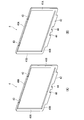
- the disassembled perspective view which showed the outline of the cell unit which concerns on this invention typically.
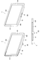
- the top view of a cell The bottom view of a 1st cell unit.
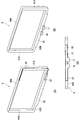
- the bottom view of a 2nd cell unit Explanatory drawing which showed typically the electrical connection state in a 1st cell unit.
- Explanatory drawing which showed typically the electrical connection state in a 2nd cell unit The disassembled perspective view which showed the 1st cell unit typically. It is explanatory drawing which showed the 1st spacer typically, Comprising: (A) is the perspective view seen from the surface side, (B) is the perspective view seen from the back surface side.
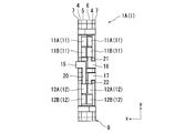
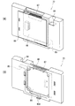
- FIG. 1 is an exploded perspective view schematically showing an outline of the cell unit 1.
- the cell unit 1 corresponds to a battery unit and has a structure in which three cells 2 are stacked.
- the cell unit 1 is composed of the end plate 7, the first spacer 4, the cell 2A, the second spacer 5, the cell 2B, the third spacer 6, the cell 2C, the first spacer 4, and the end plate 7 in this order from the left in the drawing. It has a laminated structure, and has a flat rectangular parallelepiped shape as a whole.
- the cells 2A, 2B, and 2C are accommodated in a case 8 including a pair of first spacers 4, 4, a second spacer 5, a third spacer 6, and a pair of end plates 7, 7. It has a structure.
- the stacking direction will be described below as the X axis, the horizontal direction in the figure as the Y axis, and the vertical direction in the figure as the Z axis.
- the cell 2 corresponds to a film-clad battery, and is, for example, a flat lithium ion secondary battery sealed with a film.
- a battery element formed by alternately laminating positive electrode plates (not shown) and negative electrode plates (not shown) via separators (not shown) is sandwiched between outer films, and the outer films The peripheral edge of this is heat-sealed and hermetically sealed.
- the cell 2 has a substantially rectangular flat shape.
- a single laminate film 10 serving as an exterior film is folded in two and sandwiched between the battery elements on the inside thereof.
- the remaining three sides are heat-sealed.
- the laminate film 10 is a film having a multilayer structure including at least an inner heat fusion layer, an intermediate metal layer, and an outer protective layer. The sealing of the laminate film 10 by heat sealing is performed in a form leaving an inlet for filling with the electrolytic solution, and after filling the electrolytic solution inside, the inlet portion is sealed.
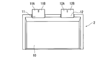
- the cell 2 in the present example has a positive electrode tab 11 and a negative electrode tab 12 as lead terminals drawn out from the long side of the heat-sealed rectangle to the outside of the laminate film 10.
- Each of the positive electrode tab 11 and the negative electrode tab 12 is cut at the distal end side, and the distal end side is divided into two forks to form distal end portions 11A, 11B, 12A, and 12B.
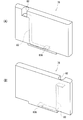
- the cell unit 1 in this embodiment is roughly divided into a first cell unit 1A for series connection as shown in FIG. 3 and a second cell unit 1B for parallel connection as shown in FIG.
- a plurality of these first cell units 1A and second cell units 1B can be arbitrarily combined and stacked to be electrically connected to each other.
- the leading end portions 11 ⁇ / b> A, 11 ⁇ / b> B, 12 ⁇ / b> A and 12 ⁇ / b> B of the positive electrode tab 11 and the negative electrode tab 12 are drawn out to the outer peripheral side of the case 8. The structure is exposed to the outside.
- the first cell unit 1A has one negative terminal (one negative electrode terminal 15 on one side (left side in FIG. 3) in the stacking direction (left-right direction in FIG. 3) (X-axis direction) when connecting the cell units 1 to each other. And has a positive electrode terminal (the other positive electrode terminal 16) and a negative electrode terminal (the other negative electrode terminal 17) on the other side (the right side in FIG. 3) in the stacking direction.
- the first cell unit 1A is formed so that a pair of terminals (one negative electrode terminal 15 and the other positive electrode terminal 16) are separated from each other in the stacking direction, and the remaining terminals (the other negative electrode terminal 17) are
- the other positive electrode terminal 16 of the pair of terminals in the stacking direction is formed at the same position in the X-axis direction and the Z-axis direction (vertical direction in the drawing).
- the negative electrode tab 12 of the cell 2 in the first cell unit 1A is connected to the one-side negative electrode terminal 15 and the other-side negative electrode terminal 17 so as to be energized.
- the positive electrode tab 11 of the cell 2 in the first cell unit 1A is connected to the other positive electrode terminal 16 so as to be energized.
- the one-side negative terminal 15 is a protruding terminal that protrudes to the side of the first cell unit 1A along the stacking direction.
- the ends of the other-side positive terminal 16 and the other-side negative terminal 17 are located in the first cell unit 1A in the stacking direction and are non-projecting terminals that do not project to the side of the first cell unit 1A. ing.
- the other side serving as a non-projecting terminal A positive electrode terminal 16 is formed.
- the projecting terminal and the non-projecting terminal are constituted by, for example, faston terminals and the like, and the projecting terminal can be fitted between the male side and the non-projecting terminal as a female side.
- the one-side negative terminal 15 is formed at the tip of an L-shaped bus bar 20 attached to the outer peripheral surface of the second spacer 5 (see FIG. 1, FIG. 7 and FIG. 9 described later).
- the other positive electrode terminal 16 is formed at the tip of an L-shaped bus bar 21 attached to the outer peripheral surface of the third spacer 6 (see FIG. 1, FIG. 7 and FIG. 10 described later).
- the other negative electrode terminal 17 is formed at the tip of an L-shaped bus bar 22 attached to the outer peripheral surface of the third spacer 6.
- the bus bars 20, 21, and 22 correspond to conductive members, and are made of, for example, a conductive metal material.
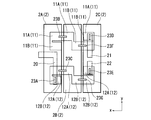
- FIG. 5 is an explanatory diagram schematically showing the electrical connection state of the cells 2A, 2B, and 2C inside the first cell unit 1A with the spacers 4, 5, and 6 omitted.
- the tip portions 11A, 11B, 12A, and 12B of the positive electrode tab 11 and the negative electrode tab 12 of the cell 2A are bent at substantially right angles toward the inner side (cell 2B side) of the first cell unit 1A.
- the cell 2A that is located outside in the stacking direction in the case 8 is the adjacent inner cell 2B.
- the tip portions 11A, 11B, 12A, and 12B are bent.
- the end portions 12A and 12B of the negative electrode tab 12 of the cell 2A are bent so as to cover the bus bar 20.
- tip part 12B of the negative electrode tab 12 of the cell 2A is welded with respect to the bus bar 20 of the 2nd spacer 5 by the welding part 23A.
- the tip portion 11A of the positive electrode tab 11 is bent at a substantially right angle toward the cell 2A so as to overlap the tip portion 11A of the positive electrode tab 11 of the cell 2A, and the tip portion 11B of the positive electrode tab 11 is It is bent at a substantially right angle toward the 2C side.
- the positive electrode tab 11 ⁇ / b> B of the cell 2 ⁇ / b> B is bent so as to cover the bus bar 21.
- the tip 12A of the negative electrode tab 12 covers the bus bar 20 and is bent toward the cell 2A so as to overlap the tip 12A of the negative electrode tab 12 of the cell 2A.
- the part 12B is bent toward the cell 2C side.
- the inner cell 2B sandwiched between the cells 2A and 2C is a cell in which the tips 11A and 12A are adjacent to each other. It is bent toward the 2A side, and the end portions 11B and 12B are bent toward the adjacent cell 2C side.
- the tip end portion 11A of the positive electrode tab 11 of the cell 2B and the tip end portion 11A of the positive electrode tab 11 of the cell 2A are welded by the welded portion 23B. Further, the tip portion 12A of the negative electrode tab 12 of the cell 2B and the tip portion 12A of the negative electrode tab 12 of the cell 2A overlap on the cell 2B side with respect to the bus bar 20, and are welded at the welded portion 23C.
- the front end portions 11A, 11B, 12A, and 12B of the positive electrode tab 11 and the negative electrode tab 12 of the cell 2C are bent at a substantially right angle toward the inner side (cell 2B side) of the first cell unit 1A.
- the cell 2C that is located outside in the stacking direction in the case 8 is the adjacent inner cell 2B.
- the tip portions 11A, 11B, 12A, and 12B are bent.
- the front end portions 11 ⁇ / b> A and 11 ⁇ / b> B of the positive electrode tab 11 of the cell 2 ⁇ / b> C are bent so as to cover the bus bar 21.
- the front end portion 12 ⁇ / b> A of the negative electrode tab 12 of the cell 2 ⁇ / b> C is bent so as to cover the bus bar 22.
- tip part 11A of the positive electrode tab 11 of the cell 2C is welded with respect to the bus bar 21 of the 3rd spacer 6 by the welding part 23D.
- the tip 12A of the negative electrode tab 12 of the cell 2C is welded to the bus bar 22 of the third spacer 6 by a weld 23E.
- the leading end portion 11B of the positive electrode tab 11 of the cell 2C and the leading end portion 11B of the positive electrode tab 11 of the cell 2B overlap each other on the cell 2B side with respect to the bus bar 21, and are welded at the welding portion 23F.
- the tip portion 12B of the negative electrode tab 12 of the cell 2C and the tip portion 12B of the negative electrode tab 12 of the cell 2B overlap each other on the cell 2B side with respect to the bus bar 22, and are welded by the welding portion 23G.
- the first cell unit 1 ⁇ / b> A, at least a part of the positive electrode tab 11, the negative electrode tab 12, and the bus bars 20, 21, and 22 of the cell 2 are exposed to the outside at one end surface of the case 8.
- the cells 2A, 2B, and 2C are electrically connected to each other in parallel.
- the second cell unit 1 ⁇ / b> B has one side (left side in FIG. 4) and the other side (left side in FIG. 4) in the stacking direction (left-right direction in FIG. 4) (X-axis direction) when connecting the cell units 1 to each other.
- the right side in FIG. 4 has one positive terminal and one negative terminal. That is, the second cell unit 1B has one side positive terminal 24 and one side negative terminal 25 on one side in the stacking direction, and the other side positive terminal 26 and the other side negative terminal 27 on the other side in the stacking direction.
- the one-side positive terminal 24 and the other-side positive terminal 26 are separated from each other in the stacking direction (X-axis direction) and are provided at the same position in the Y-axis direction and the Z-axis direction.
- the one-side negative electrode terminal 25 and the other-side negative electrode terminal 27 are separated from each other in the stacking direction (X-axis direction) and are provided at the same position in the Y-axis direction and the Z-axis direction.
- the second cell unit 1B is formed so that the one-side positive terminal 24 and the other-side negative terminal 27, and the one-side negative terminal 25 and the other-side negative terminal 27 are separated from each other in the stacking direction. Further, the one-side positive electrode terminal 24 and the other-side negative electrode terminal 27 have the same position in the Y-axis direction (vertical direction) in FIG. 4 and the same position in the Z-axis direction (vertical direction in the drawing). Further, the one-side positive terminal 24 and the other-side positive terminal 26 have the same vertical position in FIG. 4 and the vertical position in FIG. 4.
- the positive electrode tab 11 of the cell 2 in the second cell unit 1B is connected to the one-side positive electrode terminal 24 and the other-side positive electrode tab 26 so as to be energized.
- the negative electrode tab 12 of the cell 2 in the second cell unit 1B is connected to the one-side negative electrode terminal 25 and the other-side negative electrode terminal 27 so as to be energized.
- the one-side positive terminal 24 and the one-side negative terminal 25 are protruding terminals that protrude to the side of the second cell unit 1B along the stacking direction.
- the other-side positive terminal 26 and the other-side negative terminal 27 are located in the second cell unit 1B in the stacking direction and are non-projecting terminals that do not project to the side of the second cell unit 1B. Further, at the position on the back side of the one-side positive terminal 24 serving as a protruding terminal, that is, the same position in the Y-axis direction and the Z-axis direction, and at a position separated in the X-axis direction, it becomes a non-projecting terminal.
- the other positive electrode terminal 26 is formed.
- the protruding terminal and the non-protruding terminal are constituted by, for example, faston terminals and the like, and the protruding terminal is a male side and the non-protruding terminal is a female side. It is possible.
- the one-side positive terminal 24 is formed at the tip of an L-shaped bus bar 30 attached to the outer peripheral surface of the second spacer 5 (see FIG. 1 and FIGS. 7 and 9 described later).
- the one-side negative terminal 25 is formed at the tip of an L-shaped bus bar 31 attached to the outer peripheral surface of the second spacer 5.
- the other positive electrode terminal 26 is formed at the tip of an L-shaped bus bar 32 attached to the outer peripheral surface of the third spacer 6 (see FIG. 1, FIG. 7 and FIG. 10 described later).
- the other negative electrode terminal 27 is formed at the tip of an L-shaped bus bar 33 attached to the outer peripheral surface of the third spacer 6.
- the bus bars 30, 31, 32, 33 correspond to conductive members, and are made of, for example, a conductive metal material.
- FIG. 6 is an explanatory diagram schematically showing the electrical connection state of the cells 2A, 2B, and 2C inside the second cell unit 1B with the illustration of the spacers 4, 5, and 6 omitted.
- the tip portions 11A, 11B, 12A, and 12B of the positive electrode tab 11 and the negative electrode tab 12 of the cell 2A are bent at substantially right angles toward the inner side (cell 2B side) of the second cell unit 1B.
- the front end portions 11 ⁇ / b> A and 11 ⁇ / b> B of the positive electrode tab 11 of the cell 2 ⁇ / b> A are bent so as to cover the bus bar 30.
- the second cell unit 1B out of the three cells 2A, 2B, and 2C stacked in the case 8, the cell 2A located outside in the stacking direction in the case 8 is replaced with the adjacent inner cell 2B.
- the tip portions 11A, 11B, 12A, and 12B are bent.
- the end portions 12A and 12B of the negative electrode tab 12 of the cell 2A are bent so as to cover the bus bar 31.
- the front end portion 11A of the positive electrode tab 11 of the cell 2A is welded to the bus bar 30 by the welded portion 34A.
- the tip 12B of the negative electrode tab 12 of the cell 2A is welded to the bus bar 31 by a weld 34B.
- the leading end portion 11A of the positive electrode tab 11 of the cell 2B is bent at a substantially right angle toward the cell 2A side so as to cover the bus bar 30 and overlap the leading end portion 11A of the positive electrode tab 11 of the cell 2A.
- tip part 11B of the positive electrode tab 11 of the cell 2B is bent at a substantially right angle toward the cell 2C side so as to cover the bus bar 32.
- the leading end 12A of the negative electrode tab 12 covers the bus bar 31 and is bent toward the cell 2A side so as to overlap the leading end 12A of the negative electrode tab 12 of the cell 2A. Is bent toward the cell 2C side.
- the inner cell 2B sandwiched between the cells 2A and 2C is a cell in which the tips 11A and 12A are adjacent to each other. It is bent toward the 2A side, and the end portions 11B and 12B are bent toward the adjacent cell 2C side.
- the tip portion 11A of the positive electrode tab 11 of the cell 2B and the tip portion 11A of the positive electrode tab 11 of the cell 2A are welded by a welded portion 34C. More specifically, in this embodiment, the tip 11A of the positive electrode tab 11 of the cell 2B is located outside the tip 11A of the positive electrode tab 11 of the cell 2A, and the tip 11A of the positive electrode tab 11 of the cell 2A.
- the inner surface is welded to the bus bar 30, and the outer surface of the tip portion 11A of the positive electrode tab 11 of the cell 2A is welded to the tip portion 11A of the positive electrode tab 11 of the cell 2B.
- the tip 12A of the negative electrode tab 12 of the cell 2B and the tip 12A of the negative electrode tab 12 of the cell 2A overlap on the cell 2 side with respect to the bus bar 31, and are welded by the weld 34D.
- the tip portions 11A, 11B, 12A, and 12B of the positive electrode tab 11 and the negative electrode tab 12 of the cell 2C are bent substantially at right angles toward the inner side (cell 2B side) of the second cell unit 1B.
- the cell 2C positioned outside in the stacking direction in the case 8 is the adjacent inner cell 2B.
- the tip portions 11A, 11B, 12A, and 12B are bent.
- the end portions 11A and 11B of the positive electrode tab 11 of the cell 2C are bent so as to cover the bus bar 32.
- the front end portion 12 ⁇ / b> A of the negative electrode tab 12 of the cell 2 ⁇ / b> C is bent so as to cover the bus bar 33.
- the front end portion 11A of the positive electrode tab 11 of the cell 2C is welded to the bus bar 32 by the welded portion 34E.
- the tip 12A of the negative electrode tab 12 of the cell 2C is welded to the bus bar 33 by a weld 34F.
- the leading end portion 11B of the positive electrode tab 11 of the cell 2C and the leading end portion 11B of the positive electrode tab 11 of the cell 2B overlap each other on the cell 2B side with respect to the bus bar 32, and are welded by the welding portion 34G.
- the leading end 12B of the negative electrode tab 12 of the cell 2C and the leading end 12B of the negative electrode tab 12 of the cell 2B are welded by a welding portion 34H.
- the second cell unit 1 ⁇ / b> B, at least a part of the positive electrode tab 11 and the negative electrode tab 12 of the cell 2 and the bus bars 30, 31, 32, 33 are exposed to the outside at one end surface of the case 8.
- the cells 2A, 2B, and 2C are electrically connected to each other in parallel.
- first spacer 4 the configuration of the first spacer 4, the second spacer 5, the third spacer 6, and the end plate 7 will be described by taking the first cell unit 1A as an example.
- the first spacer 4, the second spacer 5, the third spacer 6, and the end plate 7 are made of, for example, an insulating synthetic resin material.
- the first spacer 4, the second spacer 5, and the third spacer 6 each have a rectangular frame shape, and the end plate 7 has a rectangular plate shape. ing.
- the first spacer 4 includes a pair of upper and lower long side portions 40A and 40B, a pair of left and right short side portions 41A and 41B, and a protruding portion 42 protruding from the lower end of the long side portion 40B to the outer peripheral side.
- a protruding portion 42 protruding from the lower end of the long side portion 40B to the outer peripheral side.
- the long side portion 40A On the upper end of the long side portion 40A, two engaging grooves 43 that engage with a locking piece 71 (described later) of the end plate 7 are formed.
- the projecting portion 42 is formed with concave portions 44, 44. That is, the recesses 44 and 44 are formed on the outer periphery of the first spacer 4.
- the second spacer 5 includes a pair of upper and lower long side portions 50A and 50B, a pair of left and right short side portions 51A and 51B, and a protruding portion 52 protruding from the lower end of the long side portion 50B to the outer peripheral side.
- An elongated recess 53 is formed on the lower surface of the protruding portion 52 along the longitudinal direction of the long side portion 50B. That is, the recess 53 is formed on the outer periphery of the second spacer 5.
- the recess 53 can accommodate the bus bar 20.
- the bus bar 20 is mounted in the recess 53, but the tip side thereof becomes the one-side negative terminal 15 and protrudes from the surface side of the second spacer 5, penetrates the recess 44 of the adjacent first spacer 4, and is more than the end plate 7. Projects outward. That is, the one-side negative terminal 15 as a protruding terminal formed at the tip of the bus bar 20 is disposed in the recess 44 of the first spacer 4 and the recess 53 of the second spacer 5.
- a thermistor 56 for temperature detection is attached to the surface side of the second spacer 5 across the long side portion 50B and the protruding portion 52.
- the lead wire 57 of the thermistor 56 is drawn out to the long side portion 50A of the second spacer 5 along the outer peripheral edge of the second spacer 5, and further extended to a battery controller 86 (not shown).
- the bus bar 30 and the bus bar 31 are attached to the second spacer 5 in the second cell unit 1B instead of the bus bar 20 as shown in FIG. It is done.
- the bus bar 30 becomes a one-side positive terminal 24 whose tip end is a protruding terminal, and protrudes to the side of the second cell unit 1B along the stacking direction.
- the bus bar 31 becomes the one-side negative terminal 25 whose tip end is a protruding terminal, and protrudes to the side of the second cell unit 1B along the stacking direction.
- the one-side positive terminal 24 as a protruding terminal formed at the tip of the bus bar 30 is disposed in the recess 44 of the first spacer 4 and the recess 53 of the second spacer 5.
- the one-side negative terminal 25 as a protruding terminal formed at the tip of the bus bar 31 is disposed in the recess 44 of the first spacer 4 and the recess 53 of the second spacer 5.
- the bus bars 30 and 31 also correspond to conductive members, and are made of, for example, a conductive metal material.
- the third spacer 6 includes a pair of upper and lower long side portions 60A and 60B, a pair of left and right short side portions 61A and 61B, and a protruding portion 62 protruding from the lower end of the long side portion 60B to the outer peripheral side.
- An elongated recess 63 is formed on the lower surface of the projecting portion 62 along the longitudinal direction of the long side portion 60B. That is, the recess 63 is formed on the outer periphery of the third spacer 6.
- the bus bars 21 and 22 can be accommodated in the recess 63.
- the bus bar 21 is mounted in the recess 63, the tip side thereof becomes the other positive electrode terminal 16 and protrudes from the back surface side of the third spacer 6, but is substantially accommodated in the recess 44 of the adjacent first spacer 4, It does not protrude outward from the end plate 7. That is, the other positive electrode terminal 16 as a non-projecting terminal formed at the tip of the bus bar 21 is disposed in the recess 44 of the first spacer 4 and the recess 63 of the third spacer 6.
- the bus bar 22 is mounted in the recess 63, the tip side thereof becomes the other negative electrode terminal 17 and protrudes from the back surface side of the third spacer 6, but is substantially accommodated in the recess 44 of the adjacent first spacer 4, It does not protrude outward from the end plate 7. That is, the other-side negative electrode terminal 17 as a non-projecting terminal formed at the tip of the bus bar 22 is disposed in the recess 44 of the first spacer 4 and the recess 63 of the third spacer 6.
- the bus bar 22 has a protruding piece 67 protruding in the opposite direction to the other negative electrode terminal 17 on the base end side.
- the protruding piece 67 is bent along the outer surface of the protruding portion 62 of the third spacer 6 and is exposed on the surface side of the third spacer 6.
- a voltage detection lead wire 69 is connected to the protruding piece 67.
- the lead wire 69 is drawn out to the long side portion 60A of the third spacer 6 along the outer peripheral edge of the third spacer 6, and further extended to a battery controller 86 (not shown). That is, the lead wire 69 constitutes a voltage detector that can detect the voltage of the first cell unit 1A from the outside of the case 8.
- a bus bar 32 and a bus bar 33 are attached instead of the bus bars 21 and 22.
- the bus bar 32 becomes the other positive electrode terminal 26 whose tip side is a non-projecting terminal, is located in the second cell unit 1B in the stacking direction, and does not project to the side of the second cell unit 1B.
- the bus bar 33 becomes the other-side negative terminal 27 whose tip side is a non-projecting terminal, is located in the second cell unit 1B in the stacking direction, and does not project to the side of the second cell unit 1B.
- the other positive electrode terminal 26 as a non-projecting terminal formed at the tip of the bus bar 32 is disposed in the concave portion 44 of the first spacer 4 and the concave portion 63 of the third spacer 6.
- the other-side negative terminal 27 as a non-projecting terminal formed at the tip of the bus bar 33 is disposed in the recess 44 of the first spacer 4 and the recess 63 of the third spacer 6.
- the bus bar 33 has a protruding piece (not shown) exposed on the surface side of the third spacer 6 on the base end side, like the bus bar 22 described above, and in the first cell unit 1A described above.
- a lead wire (not shown) for voltage detection is connected.
- the bus bars 32 and 33 also correspond to conductive members, and are made of, for example, a conductive metal material.
- the end plate 7 has four locking pieces 71 protruding from the outer peripheral edge as shown in FIG. When the first spacer 4, the second spacer 5, the third spacer 6, and the cell 2 are sandwiched, the locking pieces 71 are bent inward to hold them together.
- the first cell unit 1A and the second cell unit 1B configured as described above use the first spacer 4, the second spacer 5, the third spacer 6, and the end plate 7 having the same outer shape. Moreover, it becomes possible to contact each other between adjacent cell units 1 and 1, and when connecting cell units 1, it can connect easily, without using other members, such as a bus bar.
- the terminal provided on the back side of the projecting terminal is a non-projecting terminal and the terminal provided on the back side of the non-projecting terminal is a projecting terminal in the stacking direction, when the cell units 1 are stacked and connected, The space between the adjacent cell units 1 and 1 can be reduced, and the cell module as a battery module formed by stacking the cell units 1 can be reduced in size.
- FIG. 11 is an example of series connection composed of only the first cell unit 1A
- FIG. 12 is an example of using both serial connection and parallel connection using the first cell unit 1A and the second cell unit 1B.
- connection structure as shown in FIGS. 13 to 16 can be obtained by combining the first cell unit 1A and the second cell unit 1B, for example.
- FIG. 13 shows an example in which only the first cell unit 1A is connected.
- FIG. 14 shows an example in which six first cell units 1A and six second cell units 1B are used, and the first cell units 1A and the second cell units 1B are alternately connected.
- FIG. 15 uses four first cell units 1A and eight second cell units 1B, and alternately connects one first cell unit 1A and two second cell units 1B. This is an example.
- three first cell units 1A and nine second cell units 1B are used, and one first cell unit 1A and three second cell units 1B connected in succession. It is an example of being connected alternately.
- the number of cell units 1 and the type of cell unit 1 to be used can be set as appropriate, it is possible to easily cope with various specifications required for a cell module formed by stacking a plurality of cell units 1. it can.
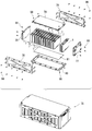
- FIG. 17 is an exploded perspective view schematically showing an outline of a cell module 75 formed by stacking 12 cell units 1.
- the cell module 75 includes a module first end plate 76 and a module second end plate 77 that sandwich 12 cell units 1 in the stacking direction, and a pair of side plates 78 that sandwich 12 cell units 1 from the side. 78, and the upper plate 79 and the lower plate 80 that sandwich the twelve cell units 1 from above and below, and by fixing these plates with a plurality of screws 98 or the like, The cell unit 1 is fixed. Further, a heat conductive sheet 81 as a heat radiating member is interposed between the lower plate 80 and the twelve cell units 1.
- the first end plate 76 for modules and the second end plate 77 for modules have a rectangular plate shape, and are made of, for example, an insulating synthetic resin material.
- the module first end plate 76 has a terminal portion 82 for taking out electric power from the cell module 75, and a bus bar 83 is embedded therein by insert molding or the like.
- the bus bar 83 is made of a conductive metal material, and is formed so that one end 83 ⁇ / b> A can be connected to the protruding terminal of the cell unit 1 in the cell module 75 and the other end extends to the terminal portion 82.
- the module second end plate 77 has a terminal portion 84 for taking out electric power from the cell module 75, and a bus bar 85 is embedded therein by insert molding or the like.
- the bus bar 85 is made of a conductive metal material, and is formed such that one end 85A can be connected to a non-projecting terminal of the cell unit 1 in the cell module 75 and the other end extends to the terminal portion 84.
- a board on which electronic components are mounted is attached to the module second end plate 77, and this board functions as the battery controller 86.
- a lead wire 57 of the thermistor 56 extended from each cell unit 1 and a lead wire 69 for voltage detection are connected to the battery controller 86 (not shown).
- 87 in FIG. 19 is a connector part for external connection provided on the board that becomes the battery controller 86
- 87 in FIG. 19 is a lid member that covers the board that becomes the battery controller 86.
- the side plate 78 has a rectangular plate shape and is made of a metal material such as iron.
- the side plate 78 is an opening except for its outer peripheral edge and its diagonal portion.
- the upper plate 79 and the lower plate 80 have a rectangular plate shape and are made of a metal material such as aluminum.
- the heat conductive sheet 81 is made of, for example, a synthetic resin material having a high heat conductivity and an insulating property.
- the heat conductive sheet 81 is continuous over the entire length of the 12 cell units 1 stacked, and directly contacts the positive electrode tab 11 and the negative electrode tab 12 of the cell 2 as shown in FIG. To do.
- the heat conductive sheet 81 can be brought into direct contact with the bus bar in the cell unit 1 by being elastically deformed when assembled. That is, the heat conductive sheet 81 can directly or indirectly contact the lead terminals (the positive electrode tab 11 and the negative electrode tab 12) of the cell 2.
- the connecting portion between the lead terminals (positive electrode tab 11 or negative electrode tab 12) between the adjacent cells 2 and 2 is flattened. Therefore, the contact area of the connecting portion between the lead terminals on the heat conductive sheet 81 can be easily increased.
- the heat of the cell unit 1 can be efficiently transmitted to the lower plate 80 via the heat conductive sheet 81 without using a complicated configuration.
- the cell unit 1 can be efficiently cooled.
- the number of cells 2 in the cell unit 1 is not limited to three.
- the number of spacers is appropriately changed so that all the cells 2 are sandwiched between the spacers.
- the number of cell units 1 in the cell module 75 is twelve, but the number of cell units 1 in the cell module 75 is not limited to twelve. As shown in 21, six cell units 1 may be provided. Therefore, the dimensions of the upper plate 79, the lower plate 80, the side plate 78, and the heat conductive sheet 81 constituting the cell module 75 may be appropriately changed according to the number of the cell units 1.
Abstract
A first cell unit (1A) is provided, on one side in the stacking direction when connecting together cell units (1), with a one-side negative electrode terminal (15) and is provided, on the other side in the stacking direction, with an other-side positive electrode terminal (16) and an other-side negative electrode terminal (17). In addition, a second cell unit (1B) is provided, on one side in the stacking direction, with a one-side positive electrode terminal (24) and a one-side negative electrode terminal (25) and is provided, on the other side in the stacking direction, with an other-side positive electrode terminal (26) and an other-side negative electrode terminal (27).
Description
本発明は、電池ユニット及び電池ユニットを積層した電池モジュールに関する。
The present invention relates to a battery unit and a battery module in which battery units are stacked.
例えば、特許文献1には、ラミネートフィルムで外装された扁平な電池をケースに収納して組電池とする一方、このような組電池を複数個積層して複合組電池とする構成が開示されている。この組電池は、扁平な直方体形状を呈し、細長い矩形のケース上面に、このケース上面の長手方向に沿って互いに離間して正極端子と負極端子とが1つずつ設けられている。
For example, Patent Document 1 discloses a configuration in which a flat battery covered with a laminate film is housed in a case to form an assembled battery, while a plurality of such assembled batteries are stacked to form a composite assembled battery. Yes. This assembled battery has a flat rectangular parallelepiped shape, and is provided with one positive terminal and one negative terminal on the upper surface of an elongated rectangular case, spaced apart from each other along the longitudinal direction of the upper surface of the case.
しかしながら、この特許文献1における組電池の正極端子及び負極端子は、上記積層方向で、上記ケース上面の略中央位置に形成されている。そのため、複合組電池を構成するにあたって、隣接する組電池間を接続するためにバスバー等の部材が必要となり、部品点数が増加してしまうという問題がある。
However, the positive electrode terminal and the negative electrode terminal of the assembled battery in Patent Document 1 are formed at a substantially central position on the upper surface of the case in the stacking direction. Therefore, when configuring the composite assembled battery, a member such as a bus bar is required to connect adjacent assembled batteries, and there is a problem that the number of parts increases.
そこで、本発明は、複数個積層して互いに接続可能な電池ユニットにおいて、複数の端子を有し、上記複数の端子のうちの少なくとも一対の端子は、当該電池ユニットの積層方向で、互いに離間するように形成され、残りの端子は、上記積層方向で上記一対の端子のいずれか一方と上記積層方向以外の方向において同じ位置に形成されることを特徴としている。
Therefore, the present invention provides a battery unit that can be connected to each other in a plurality of stacked layers, and has a plurality of terminals, and at least a pair of the terminals are separated from each other in the stacking direction of the battery units. The remaining terminals are formed at the same position in any direction other than the stacking direction as one of the pair of terminals in the stacking direction.
より具体的には、上記一対の端子は、一方が正極端子、他方が負極端子であり、上記電池ユニットは、1つ以上の正極端子と、1つ以上の負極端子を有している。
More specifically, one of the pair of terminals is a positive terminal and the other is a negative terminal, and the battery unit has one or more positive terminals and one or more negative terminals.
そして、望ましくは、上記積層方向の一方側及び他方側に位置する各端子が、上記積層方向に沿って上記電池ユニットの側方に突出する突出端子または上記積層方向で上記電池ユニット内に位置する非突出端子のいずれかであり、上記突出端子と上記非突出端子とが接合することで、隣接する電池ユニット同士を接続する。
Preferably, each terminal located on one side and the other side in the stacking direction is located in the battery unit in a protruding terminal protruding to the side of the battery unit along the stacking direction or in the stacking direction. Adjacent battery units are connected to each other by joining the protruding terminal and the non-projecting terminal.
さらに望ましくは、上記突出端子の上記積層方向以外の方向において同じ位置となる裏側となる位置に、上記非突出端子を形成する。
More preferably, the non-projecting terminal is formed at a position on the back side which is the same position in a direction other than the stacking direction of the projecting terminal.
上記電池ユニットは、より詳しくは、フィルム外装電池を複数個積層してケース内に収容したものであり、上記ケースの外側から上記フィルム外装電池の電圧を検出可能な電圧検出部を有するようにしてもよい。
More specifically, the battery unit is a unit in which a plurality of film-clad batteries are stacked and accommodated in a case, and has a voltage detection unit capable of detecting the voltage of the film-clad battery from the outside of the case. Also good.
また、上記フィルム外装電池のリード端子または、該リード端子が接続された導電部材は、上記ケースの一端面で外部に露出するよう構成してもよい。
Further, the lead terminal of the film-clad battery or the conductive member to which the lead terminal is connected may be configured to be exposed to the outside at one end face of the case.
本発明に係る電池モジュールは、このような電池ユニットを任意に複数個組み合わせて積層することで構成される。
The battery module according to the present invention is configured by stacking a combination of a plurality of such battery units.
また、このような電池モジュールには、上記電池ユニットの積層方向に連続し、複数個の電池ユニット間に跨って、上記リード端子に直接または間接的に接触する放熱性部材を設けるようにしてもよい。
Further, such a battery module may be provided with a heat dissipating member that is continuous in the stacking direction of the battery units and straddles between the plurality of battery units and that directly or indirectly contacts the lead terminals. Good.
そして、本発明によれば、電池ユニットを積層した際に、隣接する電池ユニット間で互いの端子同士を接触させることが可能となり、電池ユニット同士を連結する際にはバスバー等他部材を用いることなく容易に連結することが可能となる。
According to the present invention, when the battery units are stacked, the terminals can be brought into contact with each other between the adjacent battery units. When connecting the battery units, other members such as a bus bar are used. And can be easily connected.
以下、本発明の一実施例を図面に基づいて詳細に説明する。図1は、セルユニット1の概略を模式的に示した分解斜視図である。セルユニット1は、電池ユニットに相当するものであって、3つのセル2が積層された構造となっている。
Hereinafter, an embodiment of the present invention will be described in detail with reference to the drawings. FIG. 1 is an exploded perspective view schematically showing an outline of the cell unit 1. The cell unit 1 corresponds to a battery unit and has a structure in which three cells 2 are stacked.
すなわち、セルユニット1は、図中左からエンドプレート7、第1スペーサ4、セル2A、第2スペーサ5、セル2B、第3スペーサ6、セル2C、第1スペーサ4、エンドプレート7の順で積層された構造となっており、全体として扁平な直方体形状となっている。換言すると、セルユニット1は、一対の第1スペーサ4、4、第2スペーサ5、第3スペーサ6及び一対のエンドプレート7、7からなるケース8内に、セル2A,2B、2Cが収容された構造となっている。
That is, the cell unit 1 is composed of the end plate 7, the first spacer 4, the cell 2A, the second spacer 5, the cell 2B, the third spacer 6, the cell 2C, the first spacer 4, and the end plate 7 in this order from the left in the drawing. It has a laminated structure, and has a flat rectangular parallelepiped shape as a whole. In other words, in the cell unit 1, the cells 2A, 2B, and 2C are accommodated in a case 8 including a pair of first spacers 4, 4, a second spacer 5, a third spacer 6, and a pair of end plates 7, 7. It has a structure.
なお、説明の便宜上、この積層方向をX軸、図中水平方向をY軸、図中垂直方向をZ軸として以後説明する。
For convenience of explanation, the stacking direction will be described below as the X axis, the horizontal direction in the figure as the Y axis, and the vertical direction in the figure as the Z axis.
セル2は、フィルム外装電池に相当するものであって、例えば外装フィルムでシールされた平坦形状のリチウムイオン二次電池である。このセル2は、正極板(図示せず)と負極板(図示せず)をセパレータ(図示せず)を介して交互に積層してなる電池要素を外装フィルムの間に挟み込み、かつこの外装フィルムの周縁を加熱融着して気密に封止したものである。
The cell 2 corresponds to a film-clad battery, and is, for example, a flat lithium ion secondary battery sealed with a film. In this cell 2, a battery element formed by alternately laminating positive electrode plates (not shown) and negative electrode plates (not shown) via separators (not shown) is sandwiched between outer films, and the outer films The peripheral edge of this is heat-sealed and hermetically sealed.
詳述すると、セル2は、図2に示すように、略矩形の扁平な形状をなし、例えば、外装フィルムとなる1枚のラミネートフィルム10を2つに折り、その内側に上記電池要素に挟み込んだ上で、残りの3つの辺(矩形の2つの短辺と、1つの長辺)を熱融着することで構成される。ラミネートフィルム10は、内側の熱融着層と中間の金属層と外側の保護層とを少なくとも含む多層構造のフィルムである。なお、ラミネートフィルム10の熱融着による封止は、電解液の充填を行う注入口を残した形で行われ、電解液を内部に充填した後に、上記注入口部分が封止される。
Specifically, as shown in FIG. 2, the cell 2 has a substantially rectangular flat shape. For example, a single laminate film 10 serving as an exterior film is folded in two and sandwiched between the battery elements on the inside thereof. In addition, the remaining three sides (two short sides of the rectangle and one long side) are heat-sealed. The laminate film 10 is a film having a multilayer structure including at least an inner heat fusion layer, an intermediate metal layer, and an outer protective layer. The sealing of the laminate film 10 by heat sealing is performed in a form leaving an inlet for filling with the electrolytic solution, and after filling the electrolytic solution inside, the inlet portion is sealed.
本実施例におけるセル2は、熱融着された矩形の長辺からラミネートフィルム10の外側へ引きだされたリード端子としての正極タブ11と負極タブ12と、を有している。正極タブ11及び負極タブ12は、それぞれ先端側に切り込みが入れられて先端側が2股状に分かれており、先端部11A、11B、12A、12Bとなっている。
The cell 2 in the present example has a positive electrode tab 11 and a negative electrode tab 12 as lead terminals drawn out from the long side of the heat-sealed rectangle to the outside of the laminate film 10. Each of the positive electrode tab 11 and the negative electrode tab 12 is cut at the distal end side, and the distal end side is divided into two forks to form distal end portions 11A, 11B, 12A, and 12B.
そして、各セル2A、2B、2Cの夫々の先端部11A、11B、12A、12Bが詳しくは後述するが、第1スペーサ4、第2スペーサ5、第3スペーサ6に設けられたバスバーなどを介して電気的に接続される。
Further, the respective leading end portions 11A, 11B, 12A, and 12B of the cells 2A, 2B, and 2C will be described in detail later, but via the bus bars provided in the first spacer 4, the second spacer 5, and the third spacer 6, etc. Are electrically connected.
ここで、本実施例におけるセルユニット1は、図3に示すような直列接続用の第1セルユニット1Aと、図4に示すような並列接続用の第2セルユニット1Bとに大別され、これら第1セルユニット1Aと第2セルユニット1Bを任意に組み合わせて複数個積層して互いに電気的に接続可能となっている。
Here, the cell unit 1 in this embodiment is roughly divided into a first cell unit 1A for series connection as shown in FIG. 3 and a second cell unit 1B for parallel connection as shown in FIG. A plurality of these first cell units 1A and second cell units 1B can be arbitrarily combined and stacked to be electrically connected to each other.
また、図3、図4に示すように、セルユニット1A、1Bにおいては、正極タブ11及び負極タブ12の先端部11A、11B、12A、12Bが、ケース8の外周側に引き出されており、外部に露出した構成となっている。
As shown in FIGS. 3 and 4, in the cell units 1 </ b> A and 1 </ b> B, the leading end portions 11 </ b> A, 11 </ b> B, 12 </ b> A and 12 </ b> B of the positive electrode tab 11 and the negative electrode tab 12 are drawn out to the outer peripheral side of the case 8. The structure is exposed to the outside.
第1セルユニット1Aは、セルユニット1同士を接続する際の積層方向(図3における左右方向)(X軸方向)の一方側(図3における左側)に1つの負極端子(一方側負極端子15)を有し、上記積層方向の他方側(図3における右側)に正極端子(他方側正極端子16)と負極端子(他方側負極端子17)を有している。
The first cell unit 1A has one negative terminal (one negative electrode terminal 15 on one side (left side in FIG. 3) in the stacking direction (left-right direction in FIG. 3) (X-axis direction) when connecting the cell units 1 to each other. And has a positive electrode terminal (the other positive electrode terminal 16) and a negative electrode terminal (the other negative electrode terminal 17) on the other side (the right side in FIG. 3) in the stacking direction.
つまり、第1セルユニット1Aは、上記積層方向で、一対の端子(一方側負極端子15と他方側正極端子16)が互いに離間するように形成され、残りの端子(他方側負極端子17)は、上記積層方向で一対の端子うちの他方側正極端子16とX軸方向とZ軸方向(図中の上下方向)において同じ位置に形成されている。
That is, the first cell unit 1A is formed so that a pair of terminals (one negative electrode terminal 15 and the other positive electrode terminal 16) are separated from each other in the stacking direction, and the remaining terminals (the other negative electrode terminal 17) are The other positive electrode terminal 16 of the pair of terminals in the stacking direction is formed at the same position in the X-axis direction and the Z-axis direction (vertical direction in the drawing).
第1セルユニット1Aにおいて、一方側負極端子15及び他方側負極端子17には、第1セルユニット1A内のセル2の負極タブ12が通電可能に接続される。一方、他方側正極端子16には、第1セルユニット1A内のセル2の正極タブ11が通電可能に接続される。
In the first cell unit 1A, the negative electrode tab 12 of the cell 2 in the first cell unit 1A is connected to the one-side negative electrode terminal 15 and the other-side negative electrode terminal 17 so as to be energized. On the other hand, the positive electrode tab 11 of the cell 2 in the first cell unit 1A is connected to the other positive electrode terminal 16 so as to be energized.
そして、一方側負極端子15は、上記積層方向に沿って第1セルユニット1Aの側方に突出する突出端子となっている。他方側正極端子16及び他方側負極端子17の端部は、上記積層方向で第1セルユニット1A内に位置し、上記第1セルユニット1Aの側方に突出することのない非突出端子となっている。突出端子となる一方側負極端子15の裏側となる位置には、つまり、Y軸方向とZ軸方向において互いに同じ位置であり、X軸方向に離間した位置には、非突出端子となる他方側正極端子16が形成されている。なお、上記突出端子と上記非突出端子とは、例えばファストン端子等により構成され、上記突出端子をオス側、上記非突出端子をメス側として両者間で嵌合可能となっている。
The one-side negative terminal 15 is a protruding terminal that protrudes to the side of the first cell unit 1A along the stacking direction. The ends of the other-side positive terminal 16 and the other-side negative terminal 17 are located in the first cell unit 1A in the stacking direction and are non-projecting terminals that do not project to the side of the first cell unit 1A. ing. At the position on the back side of the one-side negative terminal 15 serving as a protruding terminal, that is, the same position in the Y-axis direction and the Z-axis direction, and at the position separated in the X-axis direction, the other side serving as a non-projecting terminal A positive electrode terminal 16 is formed. The projecting terminal and the non-projecting terminal are constituted by, for example, faston terminals and the like, and the projecting terminal can be fitted between the male side and the non-projecting terminal as a female side.
一方側負極端子15は、第2スペーサ5(図1、後述する図7、図9を参照)の外周面に取り付けられたL字形状のバスバー20の先端に形成されている。他方側正極端子16は、第3スペーサ6(図1、後述する図7、図10を参照)の外周面に取り付けられたL字形状のバスバー21の先端に形成されている。他方側負極端子17は、第3スペーサ6の外周面に取り付けられたL字形状のバスバー22の先端に形成されている。バスバー20、21、22は、導電部材に相当するものであって、例えば、導電性を有する金属材料からなっている。
The one-side negative terminal 15 is formed at the tip of an L-shaped bus bar 20 attached to the outer peripheral surface of the second spacer 5 (see FIG. 1, FIG. 7 and FIG. 9 described later). The other positive electrode terminal 16 is formed at the tip of an L-shaped bus bar 21 attached to the outer peripheral surface of the third spacer 6 (see FIG. 1, FIG. 7 and FIG. 10 described later). The other negative electrode terminal 17 is formed at the tip of an L-shaped bus bar 22 attached to the outer peripheral surface of the third spacer 6. The bus bars 20, 21, and 22 correspond to conductive members, and are made of, for example, a conductive metal material.
図5は、第1セルユニット1Aの内部におけるセル2A、2B、2Cの電気的接続状態を各スペーサ4,5、6の図示を省略して模式的に示した説明図である。
FIG. 5 is an explanatory diagram schematically showing the electrical connection state of the cells 2A, 2B, and 2C inside the first cell unit 1A with the spacers 4, 5, and 6 omitted.
セル2Aの正極タブ11及び負極タブ12の先端部11A、11B、12A、12Bは、第1セルユニット1Aの内側(セル2B側)に向かって略直角に折曲される。換言すると、第1セルユニット1Aにおいて、ケース8内に積層された3つのセル2A、2B、2Cのうち、ケース8内の積層方向で外側に位置するセル2Aは、隣接する内側のセル2Bに向かって、その先端部11A、11B、12A、12Bが折曲される。この際、セル2Aの負極タブ12の先端部12A、12Bは、バスバー20を覆うように折曲される。
The tip portions 11A, 11B, 12A, and 12B of the positive electrode tab 11 and the negative electrode tab 12 of the cell 2A are bent at substantially right angles toward the inner side (cell 2B side) of the first cell unit 1A. In other words, in the first cell unit 1A, out of the three cells 2A, 2B, and 2C stacked in the case 8, the cell 2A that is located outside in the stacking direction in the case 8 is the adjacent inner cell 2B. The tip portions 11A, 11B, 12A, and 12B are bent. At this time, the end portions 12A and 12B of the negative electrode tab 12 of the cell 2A are bent so as to cover the bus bar 20.
そして、セル2Aの負極タブ12の先端部12Bは、第2スペーサ5のバスバー20に対して溶接部23Aにて溶接される。
And the front-end | tip part 12B of the negative electrode tab 12 of the cell 2A is welded with respect to the bus bar 20 of the 2nd spacer 5 by the welding part 23A.
セル2Bにおいて、正極タブ11の先端部11Aは、セル2Aの正極タブ11の先端部11Aと重なり合うようにセル2A側に向かって略直角に折曲され、正極タブ11の先端部11Bは、セル2C側に向かって略直角に折曲される。セル2Bの正極タブ11Bは、バスバー21を覆うように折曲される。
In the cell 2B, the tip portion 11A of the positive electrode tab 11 is bent at a substantially right angle toward the cell 2A so as to overlap the tip portion 11A of the positive electrode tab 11 of the cell 2A, and the tip portion 11B of the positive electrode tab 11 is It is bent at a substantially right angle toward the 2C side. The positive electrode tab 11 </ b> B of the cell 2 </ b> B is bent so as to cover the bus bar 21.
また、セル2Bにおいて、負極タブ12の先端部12Aは、バスバー20を覆い、かつセル2Aの負極タブ12の先端部12Aと重なり合うようにセル2A側に向かって折曲され、負極タブ12の先端部12Bは、セル2C側に向かって折曲される。
In the cell 2B, the tip 12A of the negative electrode tab 12 covers the bus bar 20 and is bent toward the cell 2A so as to overlap the tip 12A of the negative electrode tab 12 of the cell 2A. The part 12B is bent toward the cell 2C side.
つまり、第1セルユニット1Aにおいて、ケース8内に積層された3つのセル2A、2B、2Cのうち、セル2A、2Cに挟み込まれた内側のセル2Bは、先端部11A、12Aが隣接するセル2A側に向かって折曲され、先端部11B、12Bが隣接するセル2C側に向かって折曲される。
That is, in the first cell unit 1A, of the three cells 2A, 2B, and 2C stacked in the case 8, the inner cell 2B sandwiched between the cells 2A and 2C is a cell in which the tips 11A and 12A are adjacent to each other. It is bent toward the 2A side, and the end portions 11B and 12B are bent toward the adjacent cell 2C side.
そして、セル2Bの正極タブ11の先端部11Aと、セル2Aの正極タブ11の先端部11Aとは、溶接部23Bにて溶接される。また、セル2Bの負極タブ12の先端部12Aと、セル2Aの負極タブ12の先端部12Aとは、バスバー20よりもセル2B側で重なり合い、溶接部23Cにて溶接される。
Then, the tip end portion 11A of the positive electrode tab 11 of the cell 2B and the tip end portion 11A of the positive electrode tab 11 of the cell 2A are welded by the welded portion 23B. Further, the tip portion 12A of the negative electrode tab 12 of the cell 2B and the tip portion 12A of the negative electrode tab 12 of the cell 2A overlap on the cell 2B side with respect to the bus bar 20, and are welded at the welded portion 23C.
セル2Cの正極タブ11及び負極タブ12の先端部11A、11B、12A、12Bは、第1セルユニット1Aの内側(セル2B側)に向かって略直角に折曲される。換言すると、第1セルユニット1Aにおいて、ケース8内に積層された3つのセル2A、2B、2Cのうち、ケース8内の積層方向で外側に位置するセル2Cは、隣接する内側のセル2Bに向かって、その先端部11A、11B、12A、12Bが折曲される。その際、セル2Cの正極タブ11の先端部11A、11Bは、バスバー21を覆うように折曲される。また、セル2Cの負極タブ12の先端部12Aは、バスバー22を覆うように折曲される。
The front end portions 11A, 11B, 12A, and 12B of the positive electrode tab 11 and the negative electrode tab 12 of the cell 2C are bent at a substantially right angle toward the inner side (cell 2B side) of the first cell unit 1A. In other words, in the first cell unit 1A, of the three cells 2A, 2B, and 2C stacked in the case 8, the cell 2C that is located outside in the stacking direction in the case 8 is the adjacent inner cell 2B. The tip portions 11A, 11B, 12A, and 12B are bent. At that time, the front end portions 11 </ b> A and 11 </ b> B of the positive electrode tab 11 of the cell 2 </ b> C are bent so as to cover the bus bar 21. Further, the front end portion 12 </ b> A of the negative electrode tab 12 of the cell 2 </ b> C is bent so as to cover the bus bar 22.
そして、セル2Cの正極タブ11の先端部11Aは、第3スペーサ6のバスバー21に対して溶接部23Dにて溶接される。セル2Cの負極タブ12の先端部12Aは、第3スペーサ6のバスバー22に対して溶接部23Eにて溶接される。セル2Cの正極タブ11の先端部11Bと、セル2Bの正極タブ11の先端部11Bとは、バスバー21よりもセル2B側で重なり合い、溶接部23Fにて溶接される。セル2Cの負極タブ12の先端部12Bと、セル2Bの負極タブ12の先端部12Bとは、バスバー22よりもセル2B側で重なり合い、溶接部23Gにて溶接される。
And the front-end | tip part 11A of the positive electrode tab 11 of the cell 2C is welded with respect to the bus bar 21 of the 3rd spacer 6 by the welding part 23D. The tip 12A of the negative electrode tab 12 of the cell 2C is welded to the bus bar 22 of the third spacer 6 by a weld 23E. The leading end portion 11B of the positive electrode tab 11 of the cell 2C and the leading end portion 11B of the positive electrode tab 11 of the cell 2B overlap each other on the cell 2B side with respect to the bus bar 21, and are welded at the welding portion 23F. The tip portion 12B of the negative electrode tab 12 of the cell 2C and the tip portion 12B of the negative electrode tab 12 of the cell 2B overlap each other on the cell 2B side with respect to the bus bar 22, and are welded by the welding portion 23G.
従って、第1セルユニット1Aにおいて、セル2の正極タブ11及び負極タブ12、バスバー20、21、22は、少なくともその一部がケース8の一端面で外部に露出している。また、第1セルユニット1Aにおいて、セル2A、2B、2Cは互いに電気的に並列に接続されている。
Therefore, in the first cell unit 1 </ b> A, at least a part of the positive electrode tab 11, the negative electrode tab 12, and the bus bars 20, 21, and 22 of the cell 2 are exposed to the outside at one end surface of the case 8. In the first cell unit 1A, the cells 2A, 2B, and 2C are electrically connected to each other in parallel.
図4に示すように、第2セルユニット1Bは、セルユニット1同士を接続する際の積層方向(図4における左右方向)(X軸方向)の一方側(図4における左側)及び他方側(図4における右側)に、それぞれ正極端子と負極端子を1つずつ有している。すなわち、第2セルユニット1Bは、上記積層方向の一方側に一方側正極端子24と一方側負極端子25を有し、上記積層方向の他方側に他方側正極端子26と他方側負極端子27を有している。
As shown in FIG. 4, the second cell unit 1 </ b> B has one side (left side in FIG. 4) and the other side (left side in FIG. 4) in the stacking direction (left-right direction in FIG. 4) (X-axis direction) when connecting the cell units 1 to each other. The right side in FIG. 4 has one positive terminal and one negative terminal. That is, the second cell unit 1B has one side positive terminal 24 and one side negative terminal 25 on one side in the stacking direction, and the other side positive terminal 26 and the other side negative terminal 27 on the other side in the stacking direction. Have.
一方側正極端子24と他方側正極端子26とが積層方向(X軸方向)に互いに離間して、Y軸方向とZ軸方向において互いに同じ位置に設けられている。また、一方側負極端子25と他方側負極端子27とが積層方向(X軸方向)に互いに離間して、Y軸方向とZ軸方向において互いに同じ位置に設けられている。
The one-side positive terminal 24 and the other-side positive terminal 26 are separated from each other in the stacking direction (X-axis direction) and are provided at the same position in the Y-axis direction and the Z-axis direction. The one-side negative electrode terminal 25 and the other-side negative electrode terminal 27 are separated from each other in the stacking direction (X-axis direction) and are provided at the same position in the Y-axis direction and the Z-axis direction.
第2セルユニット1Bは、上記積層方向で、一方側正極端子24と他方側負極端子27とが、そして一方側負極端子25と他方側負極端子27とが、互いに離間するように形成される。また、一方側正極端子24と他方側負極端子27とは、図4においてY軸方向(上下方向)の位置が同じであり、Z軸方向(図面に垂直方向)の位置が同じである。さらに、一方側正極端子24と他方側正極端子26とは、図4において上下方向の位置が同じであり、図4において垂直方向の位置が同じである。
The second cell unit 1B is formed so that the one-side positive terminal 24 and the other-side negative terminal 27, and the one-side negative terminal 25 and the other-side negative terminal 27 are separated from each other in the stacking direction. Further, the one-side positive electrode terminal 24 and the other-side negative electrode terminal 27 have the same position in the Y-axis direction (vertical direction) in FIG. 4 and the same position in the Z-axis direction (vertical direction in the drawing). Further, the one-side positive terminal 24 and the other-side positive terminal 26 have the same vertical position in FIG. 4 and the vertical position in FIG. 4.
第2セルユニット1Bにおいて、一方側正極端子24及び他方側正極タブ26には、第2セルユニット1B内のセル2の正極タブ11が通電可能に接続される。一方、一方側負極端子25及び他方側負極端子27には、第2セルユニット1B内のセル2の負極タブ12が通電可能に接続される。
In the second cell unit 1B, the positive electrode tab 11 of the cell 2 in the second cell unit 1B is connected to the one-side positive electrode terminal 24 and the other-side positive electrode tab 26 so as to be energized. On the other hand, the negative electrode tab 12 of the cell 2 in the second cell unit 1B is connected to the one-side negative electrode terminal 25 and the other-side negative electrode terminal 27 so as to be energized.
一方側正極端子24及び一方側負極端子25は、上記積層方向に沿って第2セルユニット1Bの側方に突出する突出端子となっている。他方側正極端子26及び他方側負極端子27は、上記積層方向で第2セルユニット1B内に位置し、第2セルユニット1Bの側方に突出することのない非突出端子となっている。また、突出端子となる一方側正極端子24の裏側となる位置には、つまり、Y軸方向とZ軸方向において互いに同じ位置であり、X軸方向に離間した位置には、非突出端子となる他方側正極端子26が形成されている。同様に、突出端子となる一方側負極端子25の裏側となる位置には、つまり、Y軸方向とZ軸方向において互いに同じ位置であり、X軸方向に離間した位置には、非突出端子となる他方側負極端子27が形成されている。なお、この第2セルユニット1Bにおいても、上記突出端子と上記非突出端子とは、例えばファストン端子等により構成され、上記突出端子をオス側、上記非突出端子をメス側として両者間で嵌合可能となっている。
The one-side positive terminal 24 and the one-side negative terminal 25 are protruding terminals that protrude to the side of the second cell unit 1B along the stacking direction. The other-side positive terminal 26 and the other-side negative terminal 27 are located in the second cell unit 1B in the stacking direction and are non-projecting terminals that do not project to the side of the second cell unit 1B. Further, at the position on the back side of the one-side positive terminal 24 serving as a protruding terminal, that is, the same position in the Y-axis direction and the Z-axis direction, and at a position separated in the X-axis direction, it becomes a non-projecting terminal. The other positive electrode terminal 26 is formed. Similarly, a position on the back side of the one-side negative electrode terminal 25 serving as a protruding terminal, that is, the same position in the Y-axis direction and the Z-axis direction and a position separated in the X-axis direction, The other-side negative electrode terminal 27 is formed. Also in the second cell unit 1B, the protruding terminal and the non-protruding terminal are constituted by, for example, faston terminals and the like, and the protruding terminal is a male side and the non-protruding terminal is a female side. It is possible.
一方側正極端子24は、第2スペーサ5(図1、後述する図7、図9参照)の外周面に取り付けられたL字形状のバスバー30の先端に形成されている。一方側負極端子25は、第2スペーサ5の外周面に取り付けられたL字形状のバスバー31の先端に形成されている。他方側正極端子26は、第3スペーサ6(図1、後述する図7、図10参照)の外周面に取り付けられたL字形状のバスバー32の先端に形成されている。他方側負極端子27は、第3スペーサ6の外周面に取り付けられたL字形状のバスバー33の先端に形成されている。バスバー30、31、32、33は、導電部材に相当するものであって、例えば、導電性を有する金属材料からなっている。
The one-side positive terminal 24 is formed at the tip of an L-shaped bus bar 30 attached to the outer peripheral surface of the second spacer 5 (see FIG. 1 and FIGS. 7 and 9 described later). The one-side negative terminal 25 is formed at the tip of an L-shaped bus bar 31 attached to the outer peripheral surface of the second spacer 5. The other positive electrode terminal 26 is formed at the tip of an L-shaped bus bar 32 attached to the outer peripheral surface of the third spacer 6 (see FIG. 1, FIG. 7 and FIG. 10 described later). The other negative electrode terminal 27 is formed at the tip of an L-shaped bus bar 33 attached to the outer peripheral surface of the third spacer 6. The bus bars 30, 31, 32, 33 correspond to conductive members, and are made of, for example, a conductive metal material.
図6は、第2セルユニット1Bの内部におけるセル2A、2B、2Cの電気的接続状態を各スペーサ4、5、6の図示を省略して模式的に示した説明図である。
FIG. 6 is an explanatory diagram schematically showing the electrical connection state of the cells 2A, 2B, and 2C inside the second cell unit 1B with the illustration of the spacers 4, 5, and 6 omitted.
セル2Aの正極タブ11及び負極タブ12の先端部11A、11B、12A、12Bは、第2セルユニット1Bの内側(セル2B側)に向かって略直角に折曲される。セル2Aの正極タブ11の先端部11A、11Bは、バスバー30を覆うように折曲される。換言すると、第2セルユニット1Bにおいて、ケース8内に積層された3つのセル2A、2B、2Cのうち、ケース8内の積層方向で外側に位置するセル2Aは、隣接する内側のセル2Bに向かって、その先端部11A、11B、12A、12Bが折曲される。この際、セル2Aの負極タブ12の先端部12A、12Bは、バスバー31を覆うように折曲される。
The tip portions 11A, 11B, 12A, and 12B of the positive electrode tab 11 and the negative electrode tab 12 of the cell 2A are bent at substantially right angles toward the inner side (cell 2B side) of the second cell unit 1B. The front end portions 11 </ b> A and 11 </ b> B of the positive electrode tab 11 of the cell 2 </ b> A are bent so as to cover the bus bar 30. In other words, in the second cell unit 1B, out of the three cells 2A, 2B, and 2C stacked in the case 8, the cell 2A located outside in the stacking direction in the case 8 is replaced with the adjacent inner cell 2B. The tip portions 11A, 11B, 12A, and 12B are bent. At this time, the end portions 12A and 12B of the negative electrode tab 12 of the cell 2A are bent so as to cover the bus bar 31.
そして、セル2Aの正極タブ11の先端部11Aは、バスバー30に対して溶接部34Aにて溶接される。セル2Aの負極タブ12の先端部12Bは、バスバー31に対して溶接部34Bにて溶接される。
And the front end portion 11A of the positive electrode tab 11 of the cell 2A is welded to the bus bar 30 by the welded portion 34A. The tip 12B of the negative electrode tab 12 of the cell 2A is welded to the bus bar 31 by a weld 34B.
セル2Bの正極タブ11の先端部11Aは、バスバー30を覆い、かつセル2Aの正極タブ11の先端部11Aと重なり合うようにセル2A側に向かって略直角に折曲される。また、セル2Bの正極タブ11の先端部11Bは、バスバー32を覆うように、セル2C側に向かって略直角に折曲される。
The leading end portion 11A of the positive electrode tab 11 of the cell 2B is bent at a substantially right angle toward the cell 2A side so as to cover the bus bar 30 and overlap the leading end portion 11A of the positive electrode tab 11 of the cell 2A. Moreover, the front-end | tip part 11B of the positive electrode tab 11 of the cell 2B is bent at a substantially right angle toward the cell 2C side so as to cover the bus bar 32.
セル2Bにおいて、負極タブ12の先端部12Aは、バスバー31を覆い、かつセル2Aの負極タブ12の先端部12Aと重なり合うようにセル2A側に向かって折曲され、負極タブ12の先端部12Bは、セル2C側に向かって折曲される。
In the cell 2B, the leading end 12A of the negative electrode tab 12 covers the bus bar 31 and is bent toward the cell 2A side so as to overlap the leading end 12A of the negative electrode tab 12 of the cell 2A. Is bent toward the cell 2C side.
つまり、第2セルユニット1Bにおいて、ケース8内に積層された3つのセル2A、2B、2Cのうち、セル2A、2Cに挟み込まれた内側のセル2Bは、先端部11A、12Aが隣接するセル2A側に向かって折曲され、先端部11B、12Bが隣接するセル2C側に向かって折曲される。
That is, in the second cell unit 1B, of the three cells 2A, 2B, and 2C stacked in the case 8, the inner cell 2B sandwiched between the cells 2A and 2C is a cell in which the tips 11A and 12A are adjacent to each other. It is bent toward the 2A side, and the end portions 11B and 12B are bent toward the adjacent cell 2C side.
そして、セル2Bの正極タブ11の先端部11Aと、セル2Aの正極タブ11の先端部11Aとは、溶接部34Cにて溶接される。詳述すると、本実施例では、セル2Bの正極タブ11の先端部11Aが、セル2Aの正極タブ11の先端部11Aよりも外側に位置しており、セル2Aの正極タブ11の先端部11Aの内側面がバスバー30に溶接され、セル2Aの正極タブ11の先端部11Aの外側面がセル2Bの正極タブ11の先端部11Aに溶接される。また、セル2Bの負極タブ12の先端部12Aと、セル2Aの負極タブ12の先端部12Aとは、バスバー31よりもセル2側で重なり合い、溶接部34Dにて溶接される。
Then, the tip portion 11A of the positive electrode tab 11 of the cell 2B and the tip portion 11A of the positive electrode tab 11 of the cell 2A are welded by a welded portion 34C. More specifically, in this embodiment, the tip 11A of the positive electrode tab 11 of the cell 2B is located outside the tip 11A of the positive electrode tab 11 of the cell 2A, and the tip 11A of the positive electrode tab 11 of the cell 2A. The inner surface is welded to the bus bar 30, and the outer surface of the tip portion 11A of the positive electrode tab 11 of the cell 2A is welded to the tip portion 11A of the positive electrode tab 11 of the cell 2B. Further, the tip 12A of the negative electrode tab 12 of the cell 2B and the tip 12A of the negative electrode tab 12 of the cell 2A overlap on the cell 2 side with respect to the bus bar 31, and are welded by the weld 34D.
セル2Cの正極タブ11及び負極タブ12の先端部11A、11B、12A、12Bは、第2セルユニット1Bの内側(セル2B側)に向かって略直角に折曲される。換言すると、第2セルユニット1Bにおいて、ケース8内に積層された3つのセル2A、2B、2Cのうち、ケース8内の積層方向で外側に位置するセル2Cは、隣接する内側のセル2Bに向かって、その先端部11A、11B、12A、12Bが折曲される。その際に、セル2Cの正極タブ11の先端部11A、11Bは、バスバー32を覆うように折曲される。また、セル2Cの負極タブ12の先端部12Aは、バスバー33を覆うように折曲される。
The tip portions 11A, 11B, 12A, and 12B of the positive electrode tab 11 and the negative electrode tab 12 of the cell 2C are bent substantially at right angles toward the inner side (cell 2B side) of the second cell unit 1B. In other words, in the second cell unit 1B, out of the three cells 2A, 2B, and 2C stacked in the case 8, the cell 2C positioned outside in the stacking direction in the case 8 is the adjacent inner cell 2B. The tip portions 11A, 11B, 12A, and 12B are bent. At that time, the end portions 11A and 11B of the positive electrode tab 11 of the cell 2C are bent so as to cover the bus bar 32. Further, the front end portion 12 </ b> A of the negative electrode tab 12 of the cell 2 </ b> C is bent so as to cover the bus bar 33.
そして、セル2Cの正極タブ11の先端部11Aは、バスバー32に対して溶接部34Eにて溶接される。セル2Cの負極タブ12の先端部12Aは、バスバー33に対して溶接部34Fにて溶接される。セル2Cの正極タブ11の先端部11Bと、セル2Bの正極タブ11の先端部11Bとは、バスバー32よりもセル2B側で重なり合い、溶接部34Gにて溶接される。セル2Cの負極タブ12の先端部12Bと、セル2Bの負極タブ12の先端部12Bとは、溶接部34Hにて溶接される。
And the front end portion 11A of the positive electrode tab 11 of the cell 2C is welded to the bus bar 32 by the welded portion 34E. The tip 12A of the negative electrode tab 12 of the cell 2C is welded to the bus bar 33 by a weld 34F. The leading end portion 11B of the positive electrode tab 11 of the cell 2C and the leading end portion 11B of the positive electrode tab 11 of the cell 2B overlap each other on the cell 2B side with respect to the bus bar 32, and are welded by the welding portion 34G. The leading end 12B of the negative electrode tab 12 of the cell 2C and the leading end 12B of the negative electrode tab 12 of the cell 2B are welded by a welding portion 34H.
従って、第2セルユニット1Bにおいても、セル2の正極タブ11及び負極タブ12、バスバー30、31、32、33は、少なくともその一部がケース8の一端面で外部に露出している。また、第2セルユニット1Bにおいて、セル2A、2B、2Cは互いに電気的に並列に接続されている。
Therefore, also in the second cell unit 1 </ b> B, at least a part of the positive electrode tab 11 and the negative electrode tab 12 of the cell 2 and the bus bars 30, 31, 32, 33 are exposed to the outside at one end surface of the case 8. In the second cell unit 1B, the cells 2A, 2B, and 2C are electrically connected to each other in parallel.
ここで、第1セルユニット1Aを例に、第1スペーサ4、第2スペーサ5、第3スペーサ6及びエンドプレート7の構成を説明する。
Here, the configuration of the first spacer 4, the second spacer 5, the third spacer 6, and the end plate 7 will be described by taking the first cell unit 1A as an example.
第1スペーサ4、第2スペーサ5、第3スペーサ6及びエンドプレート7は、例えば、絶縁性の合成樹脂材料からなっている。
The first spacer 4, the second spacer 5, the third spacer 6, and the end plate 7 are made of, for example, an insulating synthetic resin material.
図7に示すように、第1スペーサ4、第2スペーサ5、第3スペーサ6は、それぞれ矩形の枠状を呈し、エンドプレート7は、矩形の板状を呈している。
ている。 As shown in FIG. 7, thefirst spacer 4, the second spacer 5, and the third spacer 6 each have a rectangular frame shape, and the end plate 7 has a rectangular plate shape.
ing.
ている。 As shown in FIG. 7, the
ing.
第1スペーサ4は、図8に示すように、上下一対の長辺部40A、40Bと左右一対の短辺部41A、41Bと、長辺部40Bの下端から外周側に張り出した突出部42を有している。長辺部40Aには、その上端にエンドプレート7の係止片71(後述)と係合する2つの係合溝43が形成されている。また、突出部42には、凹部44、44が形成されている。つまり、凹部44、44は、第1スペーサ4の外周に形成されている。
As shown in FIG. 8, the first spacer 4 includes a pair of upper and lower long side portions 40A and 40B, a pair of left and right short side portions 41A and 41B, and a protruding portion 42 protruding from the lower end of the long side portion 40B to the outer peripheral side. Have. On the upper end of the long side portion 40A, two engaging grooves 43 that engage with a locking piece 71 (described later) of the end plate 7 are formed. Further, the projecting portion 42 is formed with concave portions 44, 44. That is, the recesses 44 and 44 are formed on the outer periphery of the first spacer 4.
第2スペーサ5は、図9に示すように、上下一対の長辺部50A、50Bと左右一対の短辺部51A、51Bと、長辺部50Bの下端から外周側に張り出した突出部52を有している。突出部52の下面には、長辺部50Bの長手方向に沿って細長い凹部53が形成されている。つまり、凹部53は、第2スペーサ5の外周に形成されている。この凹部53には、バスバー20が収容可能となっている。
As shown in FIG. 9, the second spacer 5 includes a pair of upper and lower long side portions 50A and 50B, a pair of left and right short side portions 51A and 51B, and a protruding portion 52 protruding from the lower end of the long side portion 50B to the outer peripheral side. Have. An elongated recess 53 is formed on the lower surface of the protruding portion 52 along the longitudinal direction of the long side portion 50B. That is, the recess 53 is formed on the outer periphery of the second spacer 5. The recess 53 can accommodate the bus bar 20.
バスバー20は、凹部53内に取り付けられるが、その先端側が一方側負極端子15となって第2スペーサ5の表面側から突出し、隣接する第1スペーサ4の凹部44を突き抜けてエンドプレート7よりも外側に突出する。つまり、バスバー20の先端に形成される突出端子としての一方側負極端子15は、第1スペーサ4の凹部44及び第2スペーサ5の凹部53に配置される。
The bus bar 20 is mounted in the recess 53, but the tip side thereof becomes the one-side negative terminal 15 and protrudes from the surface side of the second spacer 5, penetrates the recess 44 of the adjacent first spacer 4, and is more than the end plate 7. Projects outward. That is, the one-side negative terminal 15 as a protruding terminal formed at the tip of the bus bar 20 is disposed in the recess 44 of the first spacer 4 and the recess 53 of the second spacer 5.
また、第2スペーサ5の表面側には、長辺部50Bと突出部52に跨って温度検知用のサーミスタ56が取り付けられている。このサーミスタ56のリード線57は、第2スペーサ5の外周縁に沿って第2スペーサ5の長辺部50Aまで引き出され、図示はしないが後述するバッテリコントローラ86までさらに延長される。
Further, a thermistor 56 for temperature detection is attached to the surface side of the second spacer 5 across the long side portion 50B and the protruding portion 52. The lead wire 57 of the thermistor 56 is drawn out to the long side portion 50A of the second spacer 5 along the outer peripheral edge of the second spacer 5, and further extended to a battery controller 86 (not shown).
以上は、第1セルユニット1Aの場合を説明したが、第2セルユニット1Bにおける第2スペーサ5に対しては、図4に示すように、バスバー20に替えて、バスバー30とバスバー31が取り付けられる。バスバー30は、その先端側が突出端子となる一方側正極端子24となって、上記積層方向に沿って第2セルユニット1Bの側方に突出する。バスバー31は、その先端側が突出端子となる一方側負極端子25となって、上記積層方向に沿って第2セルユニット1Bの側方に突出する。つまり、バスバー30の先端に形成される突出端子としての一方側正極端子24は、第1スペーサ4の凹部44及び第2スペーサ5の凹部53に配置される。また、バスバー31の先端に形成される突出端子としての一方側負極端子25は、第1スペーサ4の凹部44及び第2スペーサ5の凹部53に配置される。なお、バスバー30、31も導電部材に相当するものであって、例えば、導電性を有する金属材料からなっている。
As described above, the case of the first cell unit 1A has been described, but the bus bar 30 and the bus bar 31 are attached to the second spacer 5 in the second cell unit 1B instead of the bus bar 20 as shown in FIG. It is done. The bus bar 30 becomes a one-side positive terminal 24 whose tip end is a protruding terminal, and protrudes to the side of the second cell unit 1B along the stacking direction. The bus bar 31 becomes the one-side negative terminal 25 whose tip end is a protruding terminal, and protrudes to the side of the second cell unit 1B along the stacking direction. That is, the one-side positive terminal 24 as a protruding terminal formed at the tip of the bus bar 30 is disposed in the recess 44 of the first spacer 4 and the recess 53 of the second spacer 5. The one-side negative terminal 25 as a protruding terminal formed at the tip of the bus bar 31 is disposed in the recess 44 of the first spacer 4 and the recess 53 of the second spacer 5. The bus bars 30 and 31 also correspond to conductive members, and are made of, for example, a conductive metal material.
また第1セルユニット1Aの場合を説明する。第3スペーサ6は、図10に示すように、上下一対の長辺部60A、60Bと左右一対の短辺部61A、61Bと、長辺部60Bの下端から外周側に張り出した突出部62を有している。この突出部62の下面には、長辺部60Bの長手方向に沿って細長い凹部63が形成されている。つまり、凹部63は、第3スペーサ6の外周に形成されている。この凹部63には、バスバー21、22が収容可能となっている。
The case of the first cell unit 1A will be described. As shown in FIG. 10, the third spacer 6 includes a pair of upper and lower long side portions 60A and 60B, a pair of left and right short side portions 61A and 61B, and a protruding portion 62 protruding from the lower end of the long side portion 60B to the outer peripheral side. Have. An elongated recess 63 is formed on the lower surface of the projecting portion 62 along the longitudinal direction of the long side portion 60B. That is, the recess 63 is formed on the outer periphery of the third spacer 6. The bus bars 21 and 22 can be accommodated in the recess 63.
バスバー21は、凹部63内に取り付けられるが、その先端側が他方側正極端子16となって第3スペーサ6の裏面側から突出するものの、隣接する第1スペーサ4の凹部44内に略収容され、エンドプレート7よりも外側に突出することはない。つまり、バスバー21の先端に形成される非突出端子としての他方側正極端子16は、第1スペーサ4の凹部44及び第3スペーサ6の凹部63に配置される。
Although the bus bar 21 is mounted in the recess 63, the tip side thereof becomes the other positive electrode terminal 16 and protrudes from the back surface side of the third spacer 6, but is substantially accommodated in the recess 44 of the adjacent first spacer 4, It does not protrude outward from the end plate 7. That is, the other positive electrode terminal 16 as a non-projecting terminal formed at the tip of the bus bar 21 is disposed in the recess 44 of the first spacer 4 and the recess 63 of the third spacer 6.
バスバー22は、凹部63内に取り付けられるが、その先端側が他方側負極端子17となって第3スペーサ6の裏面側から突出するものの、隣接する第1スペーサ4の凹部44内に略収容され、エンドプレート7よりも外側に突出することはない。つまり、バスバー22の先端に形成される非突出端子としての他方側負極端子17は、第1スペーサ4の凹部44及び第3スペーサ6の凹部63に配置される。
Although the bus bar 22 is mounted in the recess 63, the tip side thereof becomes the other negative electrode terminal 17 and protrudes from the back surface side of the third spacer 6, but is substantially accommodated in the recess 44 of the adjacent first spacer 4, It does not protrude outward from the end plate 7. That is, the other-side negative electrode terminal 17 as a non-projecting terminal formed at the tip of the bus bar 22 is disposed in the recess 44 of the first spacer 4 and the recess 63 of the third spacer 6.
また、バスバー22は、その基端側に、他方側負極端子17と反対方向に突出する突出片67を有している。この突出片67は、第3スペーサ6の突出部62の外表面に沿って折曲され、第3スペーサ6の表面側に露出している。この突出片67には、電圧検出用のリード線69が接続されている。このリード線69は、第3スペーサ6の外周縁に沿って第3スペーサ6の長辺部60Aまで引き出され、図示はしないが後述するバッテリコントローラ86までさらに延長される。つまり、このリード線69によって、ケース8の外側から第1セルユニット1Aの電圧を検出可能な電圧検出部が構成される。
The bus bar 22 has a protruding piece 67 protruding in the opposite direction to the other negative electrode terminal 17 on the base end side. The protruding piece 67 is bent along the outer surface of the protruding portion 62 of the third spacer 6 and is exposed on the surface side of the third spacer 6. A voltage detection lead wire 69 is connected to the protruding piece 67. The lead wire 69 is drawn out to the long side portion 60A of the third spacer 6 along the outer peripheral edge of the third spacer 6, and further extended to a battery controller 86 (not shown). That is, the lead wire 69 constitutes a voltage detector that can detect the voltage of the first cell unit 1A from the outside of the case 8.
ここで、第2セルユニット1Bにおける第3スペーサ6について説明する。図4に示すように、バスバー21、22に替えて、バスバー32とバスバー33が取り付けられる。バスバー32は、その先端側が非突出端子となる他方側正極端子26となって、上記積層方向で第2セルユニット1B内に位置し、第2セルユニット1Bの側方に突出することはない。バスバー33は、その先端側が非突出端子となる他方側負極端子27となって、上記積層方向で第2セルユニット1B内に位置し、第2セルユニット1Bの側方に突出することはない。つまり、バスバー32の先端に形成される非突出端子としての他方側正極端子26は、第1スペーサ4の凹部44及び第3スペーサ6の凹部63に配置される。また、バスバー33の先端に形成される非突出端子としての他方側負極端子27は、第1スペーサ4の凹部44及び第3スペーサ6の凹部63に配置される。また、バスバー33は、上述したバスバー22と同様に、その基端側に第3スペーサ6の表面側に露出する突出片(図示せず)を有しており、上述した第1セルユニット1Aにおけるバスバー22と同様に電圧検出用のリード線(図示せず)が接続される。なお、バスバー32、33も導電部材に相当するものであって、例えば、導電性を有する金属材料からなっている。
Here, the third spacer 6 in the second cell unit 1B will be described. As shown in FIG. 4, a bus bar 32 and a bus bar 33 are attached instead of the bus bars 21 and 22. The bus bar 32 becomes the other positive electrode terminal 26 whose tip side is a non-projecting terminal, is located in the second cell unit 1B in the stacking direction, and does not project to the side of the second cell unit 1B. The bus bar 33 becomes the other-side negative terminal 27 whose tip side is a non-projecting terminal, is located in the second cell unit 1B in the stacking direction, and does not project to the side of the second cell unit 1B. That is, the other positive electrode terminal 26 as a non-projecting terminal formed at the tip of the bus bar 32 is disposed in the concave portion 44 of the first spacer 4 and the concave portion 63 of the third spacer 6. The other-side negative terminal 27 as a non-projecting terminal formed at the tip of the bus bar 33 is disposed in the recess 44 of the first spacer 4 and the recess 63 of the third spacer 6. In addition, the bus bar 33 has a protruding piece (not shown) exposed on the surface side of the third spacer 6 on the base end side, like the bus bar 22 described above, and in the first cell unit 1A described above. Similarly to the bus bar 22, a lead wire (not shown) for voltage detection is connected. The bus bars 32 and 33 also correspond to conductive members, and are made of, for example, a conductive metal material.
エンドプレート7は、図7に示すように、外周縁から突出する4つの係止片71を有している。各係止片71は、第1スペーサ4、第2スペーサ5、第3スペーサ6及びセル2を挟持した際に、これらを結束する保持するために、それぞれ内側に折曲される。
The end plate 7 has four locking pieces 71 protruding from the outer peripheral edge as shown in FIG. When the first spacer 4, the second spacer 5, the third spacer 6, and the cell 2 are sandwiched, the locking pieces 71 are bent inward to hold them together.
このように構成された第1セルユニット1A及び第2セルユニット1Bは、外形が同一形状の第1スペーサ4、第2スペーサ5、第3スペーサ6、エンドプレート7を使用するので、積層した際に、隣接するセルユニット1、1間で互いの端子同士を接触させることが可能となり、セルユニット1同士を連結する際にはバスバー等の他部材を用いることなく容易に連結することができる。
The first cell unit 1A and the second cell unit 1B configured as described above use the first spacer 4, the second spacer 5, the third spacer 6, and the end plate 7 having the same outer shape. Moreover, it becomes possible to contact each other between adjacent cell units 1 and 1, and when connecting cell units 1, it can connect easily, without using other members, such as a bus bar.
また、上記積層方向で、突出端子の裏側に設けられる端子が非突出端子となり、非突出端子の裏側に設けられる端子が突出端子となっているので、セルユニット1を積層して連結した際に、隣接するセルユニット1、1間の間隔を小さくすることができ、セルユニット1を積層してなる電池モジュールとしてのセルモジュールを小型化することができる。
Moreover, since the terminal provided on the back side of the projecting terminal is a non-projecting terminal and the terminal provided on the back side of the non-projecting terminal is a projecting terminal in the stacking direction, when the cell units 1 are stacked and connected, The space between the adjacent cell units 1 and 1 can be reduced, and the cell module as a battery module formed by stacking the cell units 1 can be reduced in size.
そして、第1セルユニット1Aと第2セルユニット1Bを用いて、図11、図12に示すように、様々な接続構造を実現することができる。図11は、第1セルユニット1Aのみからなる直列接続の例であり、図12は第1セルユニット1Aと第2セルユニット1Bを用いた直列接続と並列接続を併用した例である。
And various connection structures are realizable as shown in FIG. 11, FIG. 12 using the 1st cell unit 1A and the 2nd cell unit 1B. FIG. 11 is an example of series connection composed of only the first cell unit 1A, and FIG. 12 is an example of using both serial connection and parallel connection using the first cell unit 1A and the second cell unit 1B.
12個のセルユニット1を積層する場合には、第1セルユニット1Aと第2セルユニット1Bとの組み合せで、例えば、図13~図16に示すような接続構造とすることができる。
When twelve cell units 1 are stacked, a connection structure as shown in FIGS. 13 to 16 can be obtained by combining the first cell unit 1A and the second cell unit 1B, for example.
図13は、第1セルユニット1Aのみを接続した例である。図14は、6個の第1セルユニット1Aと6個の第2セルユニット1Bを用い、第1セルユニット1Aと第2セルユニット1Bを交互に接続した例である。図15は、4個の第1セルユニット1Aと8個の第2セルユニット1Bを用い、1つの第1セルユニット1Aと、第2セルユニット1Bを2つ接続したものと、を交互に接続した例である。図16は、3個の第1セルユニット1Aと9個の第2セルユニット1Bを用い、1つの第1セルユニット1Aと、第2セルユニット1Bを3つ連続して接続したものと、を交互に接続した例である。
FIG. 13 shows an example in which only the first cell unit 1A is connected. FIG. 14 shows an example in which six first cell units 1A and six second cell units 1B are used, and the first cell units 1A and the second cell units 1B are alternately connected. FIG. 15 uses four first cell units 1A and eight second cell units 1B, and alternately connects one first cell unit 1A and two second cell units 1B. This is an example. In FIG. 16, three first cell units 1A and nine second cell units 1B are used, and one first cell unit 1A and three second cell units 1B connected in succession. It is an example of being connected alternately.
このように、セルユニット1の個数や使用するセルユニット1の種類を適宜設定できるので、複数のセルユニット1を積層してなるセルモジュールに要求される様々仕様に対して容易に対応することができる。
Thus, since the number of cell units 1 and the type of cell unit 1 to be used can be set as appropriate, it is possible to easily cope with various specifications required for a cell module formed by stacking a plurality of cell units 1. it can.
図17は、セルユニット1を12個積層してなるセルモジュール75の概略を模式的に示した分解斜視図である。
FIG. 17 is an exploded perspective view schematically showing an outline of a cell module 75 formed by stacking 12 cell units 1.
セルモジュール75は、12個のセルユニット1を上記積層方向で挟み込むモジュール用第1エンドプレート76及びモジュール用第2エンドプレート77と、12個のセルユニット1を側方から挟み込む一対のサイドプレート78、78と、12個のセルユニット1を上下方向から挟み込むアッパプレート79及びロアプレート80と、を有し、これら各プレート同士を複数のネジ98等で固定することで、積層された12個のセルユニット1を固定する。また、ロアプレート80と12個のセルユニット1との間には、放熱部材としての熱伝導シート81が介装されている。
The cell module 75 includes a module first end plate 76 and a module second end plate 77 that sandwich 12 cell units 1 in the stacking direction, and a pair of side plates 78 that sandwich 12 cell units 1 from the side. 78, and the upper plate 79 and the lower plate 80 that sandwich the twelve cell units 1 from above and below, and by fixing these plates with a plurality of screws 98 or the like, The cell unit 1 is fixed. Further, a heat conductive sheet 81 as a heat radiating member is interposed between the lower plate 80 and the twelve cell units 1.
モジュール用第1エンドプレート76及びモジュール用第2エンドプレート77は、矩形板状を呈し、例えば、絶縁性の合成樹脂材料からなっている。
The first end plate 76 for modules and the second end plate 77 for modules have a rectangular plate shape, and are made of, for example, an insulating synthetic resin material.
モジュール用第1エンドプレート76は、図18に示すように、セルモジュール75から電力を取り出すための端子部82を有すると共に、内部にバスバー83がインサート成形等により埋設されている。このバスバー83は、導電性を有する金属材料からなり、一端83Aがセルモジュール75内のセルユニット1の突出端子に接続可能で、他端が端子部82まで延長するよう形成されている。
As shown in FIG. 18, the module first end plate 76 has a terminal portion 82 for taking out electric power from the cell module 75, and a bus bar 83 is embedded therein by insert molding or the like. The bus bar 83 is made of a conductive metal material, and is formed so that one end 83 </ b> A can be connected to the protruding terminal of the cell unit 1 in the cell module 75 and the other end extends to the terminal portion 82.
モジュール用第2エンドプレート77は、図19に示すように、セルモジュール75から電力を取り出すための端子部84を有すると共に、内部にバスバー85がインサート成形等により埋設されている。このバスバー85は、導電性を有する金属材料からなり、一端85Aがセルモジュール75内のセルユニット1の非突出端子に接続可能で、他端が端子部84まで延長するように形成されている。
As shown in FIG. 19, the module second end plate 77 has a terminal portion 84 for taking out electric power from the cell module 75, and a bus bar 85 is embedded therein by insert molding or the like. The bus bar 85 is made of a conductive metal material, and is formed such that one end 85A can be connected to a non-projecting terminal of the cell unit 1 in the cell module 75 and the other end extends to the terminal portion 84.
また、モジュール用第2エンドプレート77には、電子部品が実装された基板が取り付けられており、この基板がバッテリコントローラ86として機能する。このバッテリコントローラ86には、各セルユニット1から延長されたサーミスタ56のリード線57や、電圧検出用のリード線69が図示はしないが接続される。なお、図19中の87は、バッテリコントローラ86となる基板に設けられた外部接続用のコネクタ部であり、図19中の87は、バッテリコントローラ86となる基板を覆う蓋部材である。
Further, a board on which electronic components are mounted is attached to the module second end plate 77, and this board functions as the battery controller 86. A lead wire 57 of the thermistor 56 extended from each cell unit 1 and a lead wire 69 for voltage detection are connected to the battery controller 86 (not shown). In addition, 87 in FIG. 19 is a connector part for external connection provided on the board that becomes the battery controller 86, and 87 in FIG. 19 is a lid member that covers the board that becomes the battery controller 86.
サイドプレート78は、図17に示すように、矩形の板状を呈し、例えば、鉄等の金属材料からなっている。また、サイドプレート78は、その外周縁及びその対角線上部分以外は、開口部となっている。
As shown in FIG. 17, the side plate 78 has a rectangular plate shape and is made of a metal material such as iron. The side plate 78 is an opening except for its outer peripheral edge and its diagonal portion.
アッパプレート79及びロアプレート80は、図17に示すように、矩形の板状を呈し、例えば、アルミニウム等の金属材料からなっている。
As shown in FIG. 17, the upper plate 79 and the lower plate 80 have a rectangular plate shape and are made of a metal material such as aluminum.
熱伝導シート81は、例えば、熱伝導性率が大きく、絶縁性ある合成樹脂材料からなっている。この熱伝導シート81は、12個積層されたセルユニット1の全長に亙って連続するものであって、図20に示すように、セル2の正極タブ11及び負極タブ12に対して直接接触する。
The heat conductive sheet 81 is made of, for example, a synthetic resin material having a high heat conductivity and an insulating property. The heat conductive sheet 81 is continuous over the entire length of the 12 cell units 1 stacked, and directly contacts the positive electrode tab 11 and the negative electrode tab 12 of the cell 2 as shown in FIG. To do.
また、この熱伝導シート81は、組み付け時に弾性変形することにより、セルユニット1内のバスバーに対しても直接接触することが可能となっている。つまり、熱伝導シート81は、セル2のリード端子(正極タブ11及び負極タブ12)に直接または間接的に接触可能となっている。
In addition, the heat conductive sheet 81 can be brought into direct contact with the bus bar in the cell unit 1 by being elastically deformed when assembled. That is, the heat conductive sheet 81 can directly or indirectly contact the lead terminals (the positive electrode tab 11 and the negative electrode tab 12) of the cell 2.
本実施例のセルユニット1においては、セルユニット1の下面にバスバー等の部品がなく、隣接するセル2、2間におけるリード端子(正極タブ11または負極タブ12)同士の接続部分を平坦にすることができるので、熱伝導シート81に対するリード端子同士の接続部分の接触面積を容易に大きくすることができる。
In the cell unit 1 of the present embodiment, there are no parts such as a bus bar on the lower surface of the cell unit 1, and the connecting portion between the lead terminals (positive electrode tab 11 or negative electrode tab 12) between the adjacent cells 2 and 2 is flattened. Therefore, the contact area of the connecting portion between the lead terminals on the heat conductive sheet 81 can be easily increased.
そのため、セルユニット1を用いたセルモジュール75においては、複雑な構成にすることなく、熱伝導シート81を介してセルユニット1の熱をロアプレート80に効率よく伝達することができ、ロアプレート80をヒートシンクとして作用させて、セルユニット1を効率良く冷却することができる。
Therefore, in the cell module 75 using the cell unit 1, the heat of the cell unit 1 can be efficiently transmitted to the lower plate 80 via the heat conductive sheet 81 without using a complicated configuration. As a heat sink, the cell unit 1 can be efficiently cooled.
なお、上述した実施例においては、セルユニット1内のセル2が3つであるが、セルユニット1内のセル2の数は3つに限定されるものではない。セルユニット1内のセル2が3つ以外の場合には、全てのセル2がスペーサに挟み込まれるように、スペーサの数が適宜変更されることになる。
In the above-described embodiment, there are three cells 2 in the cell unit 1, but the number of cells 2 in the cell unit 1 is not limited to three. When the number of cells 2 in the cell unit 1 is other than three, the number of spacers is appropriately changed so that all the cells 2 are sandwiched between the spacers.
また、上述した実施例においては、セルモジュール75内のセルユニット1の個数が12個であるが、セルモジュール75内のセルユニット1の個数は12個に限定されるものではなく、例えば、図21に示すように、6個のセルユニット1であってもよい。従って、セルモジュール75を構成するアッパプレート79、ロアプレート80、サイドプレート78及び熱伝導シート81は、セルユニット1の個数に応じて、その寸法を適宜変更すればよい。
In the embodiment described above, the number of cell units 1 in the cell module 75 is twelve, but the number of cell units 1 in the cell module 75 is not limited to twelve. As shown in 21, six cell units 1 may be provided. Therefore, the dimensions of the upper plate 79, the lower plate 80, the side plate 78, and the heat conductive sheet 81 constituting the cell module 75 may be appropriately changed according to the number of the cell units 1.
Claims (21)
- 複数個積層して互いに電気的に接続可能な電池ユニットにおいて、
複数の端子を有し、上記複数の端子のうちの少なくとも一対の端子は、当該電池ユニットの積層方向で、互いに離間するように形成され、残りの端子は、上記積層方向で上記一対の端子のいずれか一方と同じ位置に形成される電池ユニット。 In battery units that can be stacked and electrically connected to each other,
A plurality of terminals, at least one pair of the plurality of terminals being formed to be separated from each other in the stacking direction of the battery unit, and the remaining terminals of the pair of terminals in the stacking direction. A battery unit formed at the same position as either one. - 上記一対の端子は、一方が正極端子、他方が負極端子であり、
上記電池ユニットは、1つ以上の正極端子と、1つ以上の負極端子を有する請求項1に記載の電池ユニット。 One of the pair of terminals is a positive terminal, the other is a negative terminal,
The battery unit according to claim 1, wherein the battery unit has one or more positive terminals and one or more negative terminals. - 上記積層方向の一方側及び他方側に位置する各端子は、上記積層方向に沿って上記電池ユニットの側方に突出する突出端子または上記積層方向で上記電池ユニット内に位置する非突出端子のいずれかであり、
上記突出端子と上記非突出端子とが嵌合することで、隣接する電池ユニット同士が接続される請求項1または2に記載の電池ユニット。 Each terminal located on one side and the other side in the stacking direction is either a protruding terminal protruding to the side of the battery unit along the stacking direction or a non-projecting terminal positioned in the battery unit in the stacking direction. And
The battery unit according to claim 1 or 2, wherein adjacent battery units are connected by fitting the protruding terminal and the non-projecting terminal. - 上記突出端子の裏側となる位置には、上記非突出端子が形成されている請求項3に記載の電池ユニット。 The battery unit according to claim 3, wherein the non-projecting terminal is formed at a position on the back side of the projecting terminal.
- 上記積層方向の一方側に1つの負極端子を有し、上記積層方向の他方側に正極端子と負極端子を1つずつ有する請求項1~4のいずれかに記載の電池ユニット。 The battery unit according to any one of claims 1 to 4, further comprising one negative terminal on one side in the stacking direction and one positive terminal and one negative terminal on the other side in the stacking direction.
- 上記積層方向の一方側に1つの負極端子を有し、上記積層方向の他方側に正極端子と負極端子を1つずつ有し、上記積層方向の一方側の負極端子が上記突出端子となり、上記積層方向の他方側に正極端子及び負極端子が上記非突出端子となっている請求項4に記載の電池ユニット。 One negative terminal on one side of the stacking direction, one positive terminal and one negative terminal on the other side of the stacking direction, the negative terminal on one side of the stacking direction becomes the protruding terminal, The battery unit according to claim 4, wherein a positive electrode terminal and a negative electrode terminal are the non-projecting terminals on the other side in the stacking direction.
- 上記積層方向の一方側に位置する負極端子の裏側には、上記積層方向の他方側の正極端子が位置する請求項5または6に記載の電池ユニット。 The battery unit according to claim 5 or 6, wherein the positive electrode terminal on the other side in the stacking direction is positioned on the back side of the negative electrode terminal positioned on one side in the stacking direction.
- 上記積層方向の一方側及び他方側に正極端子と負極端子を1つずつ有する請求項1~4のいずれかに記載の電池ユニット。 The battery unit according to any one of claims 1 to 4, which has one positive terminal and one negative terminal on one side and the other side in the stacking direction.
- 上記積層方向の一方側及び他方側に正極端子と負極端子を1つずつ有し、上記積層方向の一方側の正極端子及び負極端子が上記突出端子となり、上記積層方向の他方側に正極端子及び負極端子が上記非突出端子となっている請求項4に記載の電池ユニット。 One positive terminal and one negative terminal are provided on one side and the other side in the stacking direction, the positive terminal and the negative terminal on one side in the stacking direction serve as the protruding terminals, and the positive terminal and the negative terminal on the other side in the stacking direction. The battery unit according to claim 4, wherein a negative electrode terminal is the non-projecting terminal.
- 上記積層方向の一方側に位置する負極端子の裏側には上記積層方向の他方側の負極端子が位置し、
上記積層方向の一方側に位置する正極端子の裏側には上記積層方向の他方側の正極端子が位置する請求項8または9に記載の電池ユニット。 The negative electrode terminal on the other side of the stacking direction is located on the back side of the negative electrode terminal positioned on one side of the stacking direction,
The battery unit according to claim 8 or 9, wherein the positive electrode terminal on the other side in the stacking direction is positioned on the back side of the positive electrode terminal positioned on one side in the stacking direction. - フィルム外装電池を複数個積層してケース内に収容したものであり、上記ケース内で隣接するフィルム外装電池同士は、正極となるリード端子同士が接続されると共に、負極となるリード端子同士が接続されている請求項1~10のいずれかに記載の電池ユニット。 A plurality of film-clad batteries are stacked and accommodated in a case. The adjacent film-clad batteries in the case are connected to each other with lead terminals that are positive electrodes and to lead terminals that are negative electrodes. The battery unit according to any one of claims 1 to 10.
- フィルム外装電池を複数個積層してケース内に収容したものであり、上記ケース内のフィルム外装電池は、互いに並列に接続されている請求項1~10のいずれかに記載の電池ユニット。 11. The battery unit according to claim 1, wherein a plurality of film-clad batteries are stacked and accommodated in a case, and the film-clad batteries in the case are connected in parallel to each other.
- 上記フィルム外装電池は、互いに隣接する2つの正極リード端子と、互いに隣接する2つの負極リード端子とを有し、
上記ケース内に積層されたフィルム外装電池のうち、
両外側のフィルム外装電池は、隣接する内側のフィルム外装電池側に向かって全てのリード端子が折曲されて隣接するフィルム外装電池に接続され、
他のフィルム外装電池に挟み込まれた内側のフィルム外装電池は、一方の正極リード端子及び一方の負極リード端子が隣接する一方のフィルム外装電池側に向かって折曲されて一方のフィルム外装電池に接続され、他方の正極リード端子及び他方の負極リード端子が隣接する他方のフィルム外装電池側に向かって折曲されて他方のフィルム外装電池に接続される請求項11または12に記載の電池ユニット。 The film-clad battery has two positive electrode lead terminals adjacent to each other and two negative electrode lead terminals adjacent to each other,
Of the film-clad batteries stacked in the case,
Both outer film-clad batteries are connected to adjacent film-clad batteries with all lead terminals bent toward the adjacent inner film-clad battery side,
The inner film-clad battery sandwiched between other film-clad batteries is connected to one film-clad battery by bending one positive electrode lead terminal and one negative electrode lead terminal toward the adjacent film-clad battery side. The battery unit according to claim 11 or 12, wherein the other positive electrode lead terminal and the other negative electrode lead terminal are bent toward the other adjacent film-clad battery side and connected to the other film-clad battery. - 上記ケース内に積層されたフィルム外装電池のうち、両外側のフィルム外装電池は、上記正極リード端子と上記負極リード端子のうちの少なくとも一方が、当該電池ユニットの上記複数の端子のうちの一つに接続される請求項11~13のいずれかに記載の電池ユニット Of the film-clad batteries stacked in the case, the outer film-clad batteries are such that at least one of the positive electrode lead terminal and the negative electrode lead terminal is one of the plurality of terminals of the battery unit. The battery unit according to any one of claims 11 to 13, which is connected to the battery.
- 上記電池ユニットの端子は、上記フィルム外装電池のリード端子へ向けて延設されている請求項11~14のいずれかに記載の電池ユニット。 The battery unit according to any one of claims 11 to 14, wherein a terminal of the battery unit is extended toward a lead terminal of the film-clad battery.
- 上記ケースは、複数のスペーサを有し、
上記各フィルム外装電池間には上記スペーサが配置されると共に、上記各フィルム外装電池は、上記積層方向で上記スペーサにより挟み込まれている請求項11~15のいずれかに記載の電池ユニット。 The case has a plurality of spacers,
The battery unit according to any one of claims 11 to 15, wherein the spacer is disposed between the film-clad batteries, and the film-clad batteries are sandwiched by the spacers in the stacking direction. - 上記スペーサの外周には凹部が形成され、
上記電池ユニットの端子は、上記凹部に配置されてなる請求項16に記載の電池ユニット。 A recess is formed on the outer periphery of the spacer,
The battery unit according to claim 16, wherein a terminal of the battery unit is disposed in the recess. - 上記ケースの外側から上記フィルム外装電池の電圧を検出可能な電圧検出部を有する請求項11~17のいずれかに記載の電池ユニット。 The battery unit according to any one of claims 11 to 17, further comprising a voltage detection unit capable of detecting the voltage of the film-clad battery from the outside of the case.
- 上記フィルム外装電池のリード端子または、該リード端子が接続された導電部材は、上記ケースの一端面で外部に露出するよう構成されている請求項11~18のいずれかに記載の電池ユニット。 The battery unit according to any one of claims 11 to 18, wherein the lead terminal of the film-clad battery or the conductive member connected to the lead terminal is exposed to the outside at one end face of the case.
- 請求項1~19のいずれかに記載の電池ユニットを任意に組み合わせて複数個積層してなる電池モジュール。 A battery module formed by stacking a plurality of battery units according to any one of claims 1 to 19 in any combination.
- 上記電池ユニットの積層方向に連続し、複数個の電池ユニット間に跨って、上記リード端子に直接または間接的に接触する放熱性部材を有する請求項20に記載の電池モジュール。 21. The battery module according to claim 20, further comprising a heat dissipating member that is continuous in the stacking direction of the battery units and straddles between a plurality of battery units and directly or indirectly contacts the lead terminals.
Priority Applications (4)
| Application Number | Priority Date | Filing Date | Title |
|---|---|---|---|
| PCT/JP2013/058266 WO2014147809A1 (en) | 2013-03-22 | 2013-03-22 | Battery unit and battery module having stacked battery units |
| EP13878704.9A EP2978049A4 (en) | 2013-03-22 | 2013-03-22 | Battery unit and battery module having stacked battery units |
| JP2015506502A JPWO2014147809A1 (en) | 2013-03-22 | 2013-03-22 | Battery unit and battery module in which battery units are stacked |
| US14/777,872 US20160072116A1 (en) | 2013-03-22 | 2013-03-22 | Battery unit and battery module having stacked battery units |
Applications Claiming Priority (1)
| Application Number | Priority Date | Filing Date | Title |
|---|---|---|---|
| PCT/JP2013/058266 WO2014147809A1 (en) | 2013-03-22 | 2013-03-22 | Battery unit and battery module having stacked battery units |
Publications (1)
| Publication Number | Publication Date |
|---|---|
| WO2014147809A1 true WO2014147809A1 (en) | 2014-09-25 |
Family
ID=51579539
Family Applications (1)
| Application Number | Title | Priority Date | Filing Date |
|---|---|---|---|
| PCT/JP2013/058266 WO2014147809A1 (en) | 2013-03-22 | 2013-03-22 | Battery unit and battery module having stacked battery units |
Country Status (4)
| Country | Link |
|---|---|
| US (1) | US20160072116A1 (en) |
| EP (1) | EP2978049A4 (en) |
| JP (1) | JPWO2014147809A1 (en) |
| WO (1) | WO2014147809A1 (en) |
Cited By (5)
| Publication number | Priority date | Publication date | Assignee | Title |
|---|---|---|---|---|
| EP3367462A4 (en) * | 2015-10-22 | 2018-09-26 | Nissan Motor Co., Ltd. | Battery pack |
| WO2019017062A1 (en) * | 2017-07-18 | 2019-01-24 | 矢崎総業株式会社 | Battery module and battery monitoring unit mounting structure |
| JP2019149342A (en) * | 2018-02-28 | 2019-09-05 | トヨタ自動車株式会社 | Battery pack |
| JP2021174765A (en) * | 2020-04-20 | 2021-11-01 | エスケー イノベーション カンパニー リミテッドSk Innovation Co., Ltd. | Battery module |
| JP7470073B2 (en) | 2020-04-20 | 2024-04-17 | エスケー オン カンパニー リミテッド | Battery Module |
Families Citing this family (2)
| Publication number | Priority date | Publication date | Assignee | Title |
|---|---|---|---|---|
| TW201731603A (en) * | 2016-03-02 | 2017-09-16 | Dijiya Energy Saving Tech Inc | Lithium battery conductive connection piece and forming method thereof enabling to meet the use needs of charging and discharging of large current having high amplification factor |
| GB2566169B (en) | 2016-04-03 | 2022-10-26 | Brammo Inc | Battery pack and method of manufacture |
Citations (5)
| Publication number | Priority date | Publication date | Assignee | Title |
|---|---|---|---|---|
| JPH07142041A (en) * | 1993-11-15 | 1995-06-02 | Honda Motor Co Ltd | Method and structure for preventing contact failure of terminal |
| JP2001216950A (en) * | 2000-02-02 | 2001-08-10 | Sony Corp | Chip type battery and battery pack device |
| JP2003303583A (en) | 2002-04-11 | 2003-10-24 | Nissan Motor Co Ltd | Battery pack |
| JP2009277673A (en) * | 2004-05-31 | 2009-11-26 | Nissan Motor Co Ltd | Battery pack, and method for manufacturing the same |
| JP2010232102A (en) * | 2009-03-27 | 2010-10-14 | Japan Research Institute Ltd | Battery package, battery module, and battery pack |
Family Cites Families (9)
| Publication number | Priority date | Publication date | Assignee | Title |
|---|---|---|---|---|
| JPS55149262U (en) * | 1979-04-14 | 1980-10-27 | ||
| US5140744A (en) * | 1990-06-06 | 1992-08-25 | Miller Robert D | Modular multicell battery and rack |
| US5104752A (en) * | 1990-10-15 | 1992-04-14 | Allied-Signal, Inc. | Dual, series/parallel battery cell connects |
| JPH0673860U (en) * | 1993-03-31 | 1994-10-18 | 安藤 敏行 | Power supply |
| JP2000348781A (en) * | 1999-06-04 | 2000-12-15 | Japan Storage Battery Co Ltd | Nonaqueous electrolyte battery |
| JP4661648B2 (en) * | 2005-06-16 | 2011-03-30 | 日産自動車株式会社 | Flat battery and assembled battery using the flat battery |
| JP4894198B2 (en) * | 2005-08-22 | 2012-03-14 | 日産自動車株式会社 | Assembled battery |
| CN102301502B (en) * | 2008-11-28 | 2014-10-01 | 西门子有限公司 | System For Assembling Electrical Energy Modules |
| US8632905B2 (en) * | 2010-12-13 | 2014-01-21 | Panasonic Corporation | Battery module and battery pack |
-
2013
- 2013-03-22 WO PCT/JP2013/058266 patent/WO2014147809A1/en active Application Filing
- 2013-03-22 JP JP2015506502A patent/JPWO2014147809A1/en active Pending
- 2013-03-22 EP EP13878704.9A patent/EP2978049A4/en not_active Withdrawn
- 2013-03-22 US US14/777,872 patent/US20160072116A1/en not_active Abandoned
Patent Citations (5)
| Publication number | Priority date | Publication date | Assignee | Title |
|---|---|---|---|---|
| JPH07142041A (en) * | 1993-11-15 | 1995-06-02 | Honda Motor Co Ltd | Method and structure for preventing contact failure of terminal |
| JP2001216950A (en) * | 2000-02-02 | 2001-08-10 | Sony Corp | Chip type battery and battery pack device |
| JP2003303583A (en) | 2002-04-11 | 2003-10-24 | Nissan Motor Co Ltd | Battery pack |
| JP2009277673A (en) * | 2004-05-31 | 2009-11-26 | Nissan Motor Co Ltd | Battery pack, and method for manufacturing the same |
| JP2010232102A (en) * | 2009-03-27 | 2010-10-14 | Japan Research Institute Ltd | Battery package, battery module, and battery pack |
Non-Patent Citations (1)
| Title |
|---|
| See also references of EP2978049A4 |
Cited By (8)
| Publication number | Priority date | Publication date | Assignee | Title |
|---|---|---|---|---|
| EP3367462A4 (en) * | 2015-10-22 | 2018-09-26 | Nissan Motor Co., Ltd. | Battery pack |
| US11515597B2 (en) | 2015-10-22 | 2022-11-29 | Envision Aesc Japan Ltd. | Battery pack |
| WO2019017062A1 (en) * | 2017-07-18 | 2019-01-24 | 矢崎総業株式会社 | Battery module and battery monitoring unit mounting structure |
| JP2019021500A (en) * | 2017-07-18 | 2019-02-07 | 矢崎総業株式会社 | Battery module and battery monitoring unit mounting structure |
| US11302984B2 (en) | 2017-07-18 | 2022-04-12 | Yazaki Corporation | Battery module and battery monitoring unit mounting structure |
| JP2019149342A (en) * | 2018-02-28 | 2019-09-05 | トヨタ自動車株式会社 | Battery pack |
| JP2021174765A (en) * | 2020-04-20 | 2021-11-01 | エスケー イノベーション カンパニー リミテッドSk Innovation Co., Ltd. | Battery module |
| JP7470073B2 (en) | 2020-04-20 | 2024-04-17 | エスケー オン カンパニー リミテッド | Battery Module |
Also Published As
| Publication number | Publication date |
|---|---|
| EP2978049A4 (en) | 2016-04-20 |
| US20160072116A1 (en) | 2016-03-10 |
| JPWO2014147809A1 (en) | 2017-02-16 |
| EP2978049A1 (en) | 2016-01-27 |
Similar Documents
| Publication | Publication Date | Title |
|---|---|---|
| US10763469B2 (en) | Energy storage apparatus | |
| CN107851767B (en) | Power supply device and bus bar for battery unit | |
| JP6141732B2 (en) | Battery stack and battery pack | |
| JP6794617B2 (en) | Power storage device | |
| WO2012131801A1 (en) | Battery pack | |
| TWI525886B (en) | Secondary battery pack having pcm, device comprising the same, and method for manufacturing the same | |
| JP5374979B2 (en) | Batteries and batteries | |
| WO2014147809A1 (en) | Battery unit and battery module having stacked battery units | |
| JP5831924B2 (en) | Battery pack | |
| JP5988668B2 (en) | Battery stack | |
| JP2013214497A (en) | Battery pack | |
| JP6143108B2 (en) | Power storage module | |
| JP6334725B2 (en) | Battery module including voltage sensing member having receptacle structure | |
| JP2013187046A (en) | Battery pack | |
| WO2014010419A1 (en) | Battery assembly | |
| JP6020903B2 (en) | Power storage module | |
| JP2015026424A (en) | Power storage module | |
| JP7308923B2 (en) | electrochemical cell module | |
| JP2014135162A (en) | Power storage module | |
| WO2017014046A1 (en) | Battery module and battery pack | |
| JP2018032520A (en) | Power storage device | |
| JP5904087B2 (en) | Power storage module | |
| WO2016017668A1 (en) | Electricity storage module | |
| JP7047211B2 (en) | Battery module and battery pack containing it | |
| JP6128430B2 (en) | Power storage module |
Legal Events
| Date | Code | Title | Description |
|---|---|---|---|
| 121 | Ep: the epo has been informed by wipo that ep was designated in this application |
Ref document number: 13878704 Country of ref document: EP Kind code of ref document: A1 |
|
| ENP | Entry into the national phase |
Ref document number: 2015506502 Country of ref document: JP Kind code of ref document: A |
|
| WWE | Wipo information: entry into national phase |
Ref document number: 2013878704 Country of ref document: EP |
|
| NENP | Non-entry into the national phase |
Ref country code: DE |