WO2014130668A1 - Catalytic atomic layer deposition of films comprising sioc - Google Patents

Catalytic atomic layer deposition of films comprising sioc Download PDF

Info

Publication number
WO2014130668A1
WO2014130668A1 PCT/US2014/017391 US2014017391W WO2014130668A1 WO 2014130668 A1 WO2014130668 A1 WO 2014130668A1 US 2014017391 W US2014017391 W US 2014017391W WO 2014130668 A1 WO2014130668 A1 WO 2014130668A1
Authority
WO
WIPO (PCT)
Prior art keywords
precursor
film
substrate
catalyst
sioc
Prior art date
Legal status (The legal status is an assumption and is not a legal conclusion. Google has not performed a legal analysis and makes no representation as to the accuracy of the status listed.)
Ceased
Application number
PCT/US2014/017391
Other languages
French (fr)
Inventor
David Thompson
Jeffrey W. Anthis
Current Assignee (The listed assignees may be inaccurate. Google has not performed a legal analysis and makes no representation or warranty as to the accuracy of the list.)
Applied Materials Inc
Original Assignee
Applied Materials Inc
Priority date (The priority date is an assumption and is not a legal conclusion. Google has not performed a legal analysis and makes no representation as to the accuracy of the date listed.)
Filing date
Publication date
Application filed by Applied Materials Inc filed Critical Applied Materials Inc
Priority to US14/769,722 priority Critical patent/US20160002782A1/en
Priority to KR1020157025636A priority patent/KR20150125674A/en
Publication of WO2014130668A1 publication Critical patent/WO2014130668A1/en
Anticipated expiration legal-status Critical
Ceased legal-status Critical Current

Links

Classifications

    • CCHEMISTRY; METALLURGY
    • C23COATING METALLIC MATERIAL; COATING MATERIAL WITH METALLIC MATERIAL; CHEMICAL SURFACE TREATMENT; DIFFUSION TREATMENT OF METALLIC MATERIAL; COATING BY VACUUM EVAPORATION, BY SPUTTERING, BY ION IMPLANTATION OR BY CHEMICAL VAPOUR DEPOSITION, IN GENERAL; INHIBITING CORROSION OF METALLIC MATERIAL OR INCRUSTATION IN GENERAL
    • C23CCOATING METALLIC MATERIAL; COATING MATERIAL WITH METALLIC MATERIAL; SURFACE TREATMENT OF METALLIC MATERIAL BY DIFFUSION INTO THE SURFACE, BY CHEMICAL CONVERSION OR SUBSTITUTION; COATING BY VACUUM EVAPORATION, BY SPUTTERING, BY ION IMPLANTATION OR BY CHEMICAL VAPOUR DEPOSITION, IN GENERAL
    • C23C16/00Chemical coating by decomposition of gaseous compounds, without leaving reaction products of surface material in the coating, i.e. chemical vapour deposition [CVD] processes
    • C23C16/44Chemical coating by decomposition of gaseous compounds, without leaving reaction products of surface material in the coating, i.e. chemical vapour deposition [CVD] processes characterised by the method of coating
    • C23C16/455Chemical coating by decomposition of gaseous compounds, without leaving reaction products of surface material in the coating, i.e. chemical vapour deposition [CVD] processes characterised by the method of coating characterised by the method used for introducing gases into reaction chamber or for modifying gas flows in reaction chamber
    • C23C16/45523Pulsed gas flow or change of composition over time
    • C23C16/45525Atomic layer deposition [ALD]
    • C23C16/45527Atomic layer deposition [ALD] characterized by the ALD cycle, e.g. different flows or temperatures during half-reactions, unusual pulsing sequence, use of precursor mixtures or auxiliary reactants or activations
    • C23C16/45534Use of auxiliary reactants other than used for contributing to the composition of the main film, e.g. catalysts, activators or scavengers
    • CCHEMISTRY; METALLURGY
    • C23COATING METALLIC MATERIAL; COATING MATERIAL WITH METALLIC MATERIAL; CHEMICAL SURFACE TREATMENT; DIFFUSION TREATMENT OF METALLIC MATERIAL; COATING BY VACUUM EVAPORATION, BY SPUTTERING, BY ION IMPLANTATION OR BY CHEMICAL VAPOUR DEPOSITION, IN GENERAL; INHIBITING CORROSION OF METALLIC MATERIAL OR INCRUSTATION IN GENERAL
    • C23CCOATING METALLIC MATERIAL; COATING MATERIAL WITH METALLIC MATERIAL; SURFACE TREATMENT OF METALLIC MATERIAL BY DIFFUSION INTO THE SURFACE, BY CHEMICAL CONVERSION OR SUBSTITUTION; COATING BY VACUUM EVAPORATION, BY SPUTTERING, BY ION IMPLANTATION OR BY CHEMICAL VAPOUR DEPOSITION, IN GENERAL
    • C23C16/00Chemical coating by decomposition of gaseous compounds, without leaving reaction products of surface material in the coating, i.e. chemical vapour deposition [CVD] processes
    • C23C16/22Chemical coating by decomposition of gaseous compounds, without leaving reaction products of surface material in the coating, i.e. chemical vapour deposition [CVD] processes characterised by the deposition of inorganic material, other than metallic material
    • C23C16/30Deposition of compounds, mixtures or solid solutions, e.g. borides, carbides, nitrides
    • HELECTRICITY
    • H10SEMICONDUCTOR DEVICES; ELECTRIC SOLID-STATE DEVICES NOT OTHERWISE PROVIDED FOR
    • H10PGENERIC PROCESSES OR APPARATUS FOR THE MANUFACTURE OR TREATMENT OF DEVICES COVERED BY CLASS H10
    • H10P14/00Formation of materials, e.g. in the shape of layers or pillars
    • H10P14/60Formation of materials, e.g. in the shape of layers or pillars of insulating materials
    • H10P14/63Formation of materials, e.g. in the shape of layers or pillars of insulating materials characterised by the formation processes
    • H10P14/6326Deposition processes
    • H10P14/6328Deposition from the gas or vapour phase
    • H10P14/6334Deposition from the gas or vapour phase using decomposition or reaction of gaseous or vapour phase compounds, i.e. chemical vapour deposition
    • H10P14/6338Deposition from the gas or vapour phase using decomposition or reaction of gaseous or vapour phase compounds, i.e. chemical vapour deposition the reactions being activated by other means than plasma or thermal, e.g. photo-CVD
    • HELECTRICITY
    • H10SEMICONDUCTOR DEVICES; ELECTRIC SOLID-STATE DEVICES NOT OTHERWISE PROVIDED FOR
    • H10PGENERIC PROCESSES OR APPARATUS FOR THE MANUFACTURE OR TREATMENT OF DEVICES COVERED BY CLASS H10
    • H10P14/00Formation of materials, e.g. in the shape of layers or pillars
    • H10P14/60Formation of materials, e.g. in the shape of layers or pillars of insulating materials
    • H10P14/63Formation of materials, e.g. in the shape of layers or pillars of insulating materials characterised by the formation processes
    • H10P14/6326Deposition processes
    • H10P14/6328Deposition from the gas or vapour phase
    • H10P14/6334Deposition from the gas or vapour phase using decomposition or reaction of gaseous or vapour phase compounds, i.e. chemical vapour deposition
    • H10P14/6339Deposition from the gas or vapour phase using decomposition or reaction of gaseous or vapour phase compounds, i.e. chemical vapour deposition deposition by cyclic CVD, e.g. ALD, ALE or pulsed CVD
    • HELECTRICITY
    • H10SEMICONDUCTOR DEVICES; ELECTRIC SOLID-STATE DEVICES NOT OTHERWISE PROVIDED FOR
    • H10PGENERIC PROCESSES OR APPARATUS FOR THE MANUFACTURE OR TREATMENT OF DEVICES COVERED BY CLASS H10
    • H10P14/00Formation of materials, e.g. in the shape of layers or pillars
    • H10P14/60Formation of materials, e.g. in the shape of layers or pillars of insulating materials
    • H10P14/66Formation of materials, e.g. in the shape of layers or pillars of insulating materials characterised by the type of materials
    • H10P14/668Formation of materials, e.g. in the shape of layers or pillars of insulating materials characterised by the type of materials the materials being characterised by the deposition precursor materials
    • H10P14/6681Formation of materials, e.g. in the shape of layers or pillars of insulating materials characterised by the type of materials the materials being characterised by the deposition precursor materials the precursor containing a compound comprising Si
    • H10P14/6682Formation of materials, e.g. in the shape of layers or pillars of insulating materials characterised by the type of materials the materials being characterised by the deposition precursor materials the precursor containing a compound comprising Si the compound being a silane, e.g. disilane, methylsilane or chlorosilane
    • HELECTRICITY
    • H10SEMICONDUCTOR DEVICES; ELECTRIC SOLID-STATE DEVICES NOT OTHERWISE PROVIDED FOR
    • H10PGENERIC PROCESSES OR APPARATUS FOR THE MANUFACTURE OR TREATMENT OF DEVICES COVERED BY CLASS H10
    • H10P14/00Formation of materials, e.g. in the shape of layers or pillars
    • H10P14/60Formation of materials, e.g. in the shape of layers or pillars of insulating materials
    • H10P14/69Inorganic materials
    • H10P14/692Inorganic materials composed of oxides, glassy oxides or oxide-based glasses
    • H10P14/6921Inorganic materials composed of oxides, glassy oxides or oxide-based glasses containing silicon
    • H10P14/6922Inorganic materials composed of oxides, glassy oxides or oxide-based glasses containing silicon the material containing Si, O and at least one of H, N, C, F or other non-metal elements, e.g. SiOC, SiOC:H or SiONC

Definitions

  • the present invention relates generally to methods of depositing thin films.
  • the invention relates to atomic layer deposition processes for the deposition of SiOC films.
  • ALD atomic layer deposition
  • ALD has been used to deposit metals and metal compounds on substrate surfaces.
  • A1 2 0 3 deposition is an example of a typical ALD process illustrating the sequential and self-limiting reactions characteristic of ALD.
  • A1 2 0 3 ALD conventionally uses trimethylaluminum (TMA, often referred to as reaction “A” or the “A” precursor) and H 2 0 (often referred to as the "B” reaction or the “B” precursor).
  • TMA trimethylaluminum
  • H 2 0 often referred to as the "B” reaction or the "B” precursor
  • step A of the binary reaction hydroxyl surface species react with vapor phase TMA to produce surface-bound A10A1(CH ) 2 and CH 4 in the gas phase. This reaction is self-limited by the number of reactive sites on the surface.
  • step B of the binary reaction A1CH 3 of the surface-bound compound reacts with vapor phase H 2 0 to produce AIOH bound to the surface and CH 4 in the gas phase.
  • This reaction is self-limited by the finite number of available reactive sites on surface-bound A10A1(CH 3 ) 2 .
  • catalysts have been used during some ALD processes. The catalyst is used to activate a reaction between two or more species during the deposition process.
  • One process involving catalytic ALD involves the deposition of Si0 2 using water and SiCl 4 .
  • new catalytic ALD methods for other films are desired.
  • One aspect of the invention relates to a method of depositing a film.
  • the method comprises exposing a substrate surface to a first and second precursor in the presence of a catalyst comprising a neutral two electron donor base, the first precursor having a formula (X y H 3 _ y Si) z CH 4 _ z or (X y H _ y Si)(CH 2 ) n (SiX y H _ y ), wherein X is a halogen, y has a value of between 1 and 3, and z has a value of between 1 and 3, and n has a value between 2 and 5, and the second precursor comprising water or a compound containing carbon and at least two hydroxyl groups.
  • each X is independently selected from CI, Br and I.
  • the first precursor has a formula (X y H _ y Si) z CH 4 _ z .
  • the first precursor has a structure represented by:
  • the first precursor comprises bis(trichlorosilyl)methane.
  • the first precursor has a formula (X y H 3 _ y Si)(CH 2 ) n (SiX y H 3 _ y ).
  • n has a value of 2 or 3.
  • the catalyst comprises an amine. In one or more embodiments, the catalyst comprises pyridine or NH . In some embodiments, the second precursor comprises a diol. In one or more embodiments, the diol comprises ethylene glycol, propylene glycol and butane- 1,4-diol. In some embodiments, a film comprising SiOC is provided.
  • Another aspect of the invention relates to a method of depositing a film, the method comprising exposing a substrate surface to a first and second precursor in the presence of a catalyst comprising a neutral two electron donor base, the first precursor comprising SiX 4 or X 3 Si-SiX 3 , wherein X is a halide, and the second precursor comprises a compound containing carbon and at least two hydroxyl groups to provide a film comprising SiOC.
  • X is selected from the group consisting of CI, Br and I.
  • the first precursor comprising SiX 4 .
  • the catalyst comprises an amine.
  • the catalyst comprises pyridine or NH 3 .
  • the second precursor is a diol.
  • the diol comprises ethylene glycol, propylene glycol and butane- 1,4-diol.
  • a third aspect of the invention relates to a method of depositing a film, the method comprising exposing a substrate surface to a first and second precursor in the presence of a catalyst comprising an pyridine, the first precursor comprising bis(trichlorosilyl)methane and the second precursor comprising water.
  • FIG. shows an exemplary pulse sequence according to one or more embodiments of the invention
  • FIG. 2 shows a depth profile of the elemental content of a film deposited according to one or more embodiments of the invention
  • FIG. 3 shows a transmission electron microscope image of a film deposited according to one or more embodiments of the invention over a photoresist substrate
  • FIG 4 shows a transmission electron microscope image of a film deposited according to one or more embodiments of the invention over a silicon substrate; and [0016] FIG 5 shows a transmission electron microscope image of a film deposited according to one or more embodiments of the invention over blanket Si(100).
  • a "substrate” as used herein, refers to any substrate or material surface formed on a substrate upon which film processing is performed during a fabrication process.
  • a substrate surface on which processing can be performed include materials such as silicon, silicon oxide, strained silicon, silicon on insulator (SOI), carbon doped silicon oxides, silicon nitride, doped silicon, germanium, gallium arsenide, glass, sapphire, and any other materials such as metals, metal nitrides, metal alloys, and other conductive materials, depending on the application.
  • Substrates include, without limitation, semiconductor wafers.
  • Substrates may be exposed to a pretreatment process to polish, etch, reduce, oxidize, hydroxylate, anneal and/or bake the substrate surface.
  • any of the film processing steps disclosed may also be performed on an underlayer formed on the substrate as disclosed in more detail below, and the term "substrate surface" is intended to include such underlayer as the context indicates.
  • SiOC films can be deposited using certain silicon precursors which contain a halogen and a second precursor selected from water or a diol. Either the diol or silicon precursor may contain carbon, which ends up incorporated into the film. Such SiOC films can exhibit better dielectric constants than the conventional Si0 2 films. Specifically, the carbon content can lower the dielectric constant, which lowers leakage at a transistor level. [0020] Accordingly, one aspect of the invention relates to method of depositing a film.
  • the method comprises exposing a substrate surface to a first and second precursor in the presence of a catalyst comprising a neutral two electron donor base, the first precursor having a formula (X y H3_ y Si) z CH 4 _ z , or (X y H3_ y Si)(CH 2 ) n (SiX y H 3 _ y ), wherein X is a halogen, y has a value of between 1 and 3, and z has a value of between 1 and 3, and n has a value between 2 and 5, and the second precursor comprising water or a compound containing carbon and at least two hydroxyl groups.
  • a film comprising SiOC is provided.
  • the first precursor is a silicon precursor, and can act as both a silicon and carbon source.
  • the first precursor has a formula (X y H3_ y Si) z CH 4 _ z .
  • each X is independently selected from CI, Br and I.
  • embodiments at least one of the X groups is CI.
  • all X groups are CI.
  • Such a compound is known as bis(trichlorosilyl)methane, hexachlorodisilylmethylene, 1,1' -methylenebis( 1 ,1,1 -trichlorosilane), or methylenebis(trichlorosilane), and has a structure represented by:
  • Suitable precursors include, but are not limited to those having a structure represented by:
  • the first precursor has a formula (X y H3_ y Si)(CH 2 ) n (SiX y H3_ y ).
  • n has a value of 2 or 3, or in even further embodiments, 2.
  • Compounds of this formula may be used to further increase the carbon content, as the starting C:Si ratio will be higher.
  • each X is independently selected from CI, Br and I.
  • embodiments at least one of the X groups is CI.
  • all X groups are CI.
  • the second precursor may comprise water. In embodiments where the second precursor comprises water, the resulting film will still contain carbon from the first precursor.
  • the second precursor comprises a compound containing carbon and at least two hydroxyl groups.
  • the second precursor comprises a diol.
  • diols may be used which contain carbon.
  • carbon incorporated into the film may come from both the first and second precursors.
  • Suitable second precursors include, but are not limited to, ethylene glycol, propylene glycol and butane- 1,4-diol.
  • the diol comprises ethylene glycol. While not wishing to be bound to any particular theory, it is thought that at least two hydroxyl groups are necessary in order to allow for subsequent deposition cycles.
  • first and second precursors can be selected to tune the amount of carbon in the deposited film. The higher the carbon: silicon ratio of the precursors, the higher the ratio will be in the resulting SiOC film. For example, in embodiments where the first precursor has formula (X y H 3 _ y Si)(CH 2 ) n (SiX y H 3 _ y ), longer carbon chains can be selected to result in a higher carbon content in the deposited film. In one or more embodiments, the carbon content of the film is about 10%.
  • the catalyst comprises a neutral two electron donor base.
  • the catalyst comprises an amine.
  • the catalyst comprises a tertiary amine.
  • the catalyst comprises pyridine.
  • the catalyst comprises NH 3 .
  • a tertiary amine with a vapor pressure lower than pyridine (which is less than about 20 torr at 20 °C) can be used.
  • the method comprises exposing a substrate surface to a first and second precursor in the presence of a catalyst comprising an amine, the first precursor comprising bis(trichlorosilyl)methane and the second precursor comprising water.
  • the catalyst comprises pyridine.
  • a film comprising SiOC is provided.
  • Another aspect of the invention relates to a method of depositing a film, the method comprising a substrate surface to a first and second precursor in the presence of a catalyst comprising a neutral two electron donor base, the first precursor comprising SiX 4 or X 3 Si-SiX 3 , wherein X is a halide, and the second precursor comprising a compound containing carbon and at least two diols.
  • the first precursor is a silicon precursor.
  • the first precursor comprises SiX 4 .
  • the first precursor comprises X 3 Si-SiX 3 .
  • each X is independently selected from CI, Br and I.
  • embodiments at least one of the X groups is CI.
  • all X groups are CI.
  • the compound is Cl 3 Si-SiCl 3 , also known as hexachlorodisilane.
  • the silicon precursor is selected from SiCl 4 , SiBr 4 , or S1I 4 .
  • the second precursor comprises carbon and at least two hydroxyl groups. Carbon may be incorporated into the deposited film from the second precursor. Accordingly, in one or more embodiments, the resulting film comprises SiOC. In some embodiments, the second precursor may comprise a diol. Suitable second precursors, include, but are not limited to, ethylene glycol, propylene glycol and butane- 1,4-diol. In further embodiments, the diol comprises ethylene glycol. Again, as discussed above, it is thought that at least two OH groups are needed to repeat the cycle and get additional deposition.
  • the catalyst comprises a neutral two electron donor base.
  • the catalyst comprises an amine.
  • the catalyst comprises a tertiary amine.
  • the catalyst comprises pyridine.
  • the catalyst comprises NH 3 .
  • a tertiary amine with a vapor pressure lower than pyridine (which is less than about 20 torr at 20 °C) can be used.
  • the precursors may be flowed and/or exposed to the substrate surface either sequentially or substantially simultaneously. In embodiments where the substrate is exposed to the precursors sequentially, the process may be repeated up until a desired film thickness has been achieved. As used herein, “substantially simultaneously” refers to either co-flow or where there is merely overlap between exposures of the precursors.
  • the catalyst is added with any one or more of the reactants. In other embodiments, the catalyst is added alone, before and/or after any of the precursors.
  • the reaction conditions for the ALD reaction will be selected based on the properties of the film precursors, substrate surface, and the catalyst.
  • the deposition may be carried out at atmospheric pressure, but may also be carried out at reduced pressure.
  • the vapor pressure of the catalyst should be low enough to be practical in such applications.
  • the substrate temperature should be low enough to keep the bonds of the substrate surface intact and to prevent thermal decomposition of gaseous reactants. However, the substrate temperature should also be high enough to keep the film precursors in the gaseous phase and to provide sufficient energy for surface reactions.
  • the specific temperature depends on the specific substrate, film precursors, and catalyst used and pressure. The properties of the specific substrate, film precursors, and catalyst may be evaluated using methods known in the art, allowing selection of appropriate temperature and pressure for the reaction.
  • the deposition is carried out at a temperature less than about 400, 350, 300, 250, 200, 150, 125, or 100 °C. In some embodiments, the deposition is carried out at a temperature in the range of about 70 to about 100 °C, about 70 to about 125 °C or about 70 to about 125 °C.
  • the substrate is subjected to processing prior to and/or after forming the layer.
  • This processing can be performed in the same chamber or in one or more separate processing chambers.
  • the substrate is moved from the first chamber to a separate, second chamber for further processing.
  • the substrate can be moved directly from the first chamber to the separate processing chamber, or it can be moved from the first chamber to one or more transfer chambers, and then moved to the desired separate processing chamber.
  • the processing apparatus may comprise multiple chambers in communication with a transfer station. An apparatus of this sort may be referred to as a "cluster tool" or "clustered system,” and the like.
  • a cluster tool is a modular system comprising multiple chambers which perform various functions including substrate center-finding and orientation, degassing, annealing, deposition and/or etching.
  • a cluster tool includes at least a first chamber and a central transfer chamber.
  • the central transfer chamber may house a robot that can shuttle substrates between and among processing chambers and load lock chambers.
  • the transfer chamber is typically maintained at a vacuum condition and provides an intermediate stage for shuttling substrates from one chamber to another and/or to a load lock chamber positioned at a front end of the cluster tool.
  • processing chambers which may be used include, but are not limited to, cyclical layer deposition (CLD), atomic layer deposition (ALD), chemical vapor deposition (CVD), physical vapor deposition (PVD), etch, pre-clean, chemical clean, thermal treatment such as RTP, plasma nitridation, degas, orientation, hydroxylation and other substrate processes.
  • CLD cyclical layer deposition
  • ALD atomic layer deposition
  • CVD chemical vapor deposition
  • PVD physical vapor deposition
  • etch pre-clean
  • thermal treatment such as RTP, plasma nitridation, degas, orientation, hydroxylation and other substrate processes.
  • the substrate is continuously under vacuum or "load lock” conditions, and is not exposed to ambient air when being moved from one chamber to the next.
  • the transfer chambers are thus under vacuum and are "pumped down” under vacuum pressure.
  • Inert gases may be present in the processing chambers or the transfer chambers.
  • an inert gas is used as a purge gas to remove some or all of the reactants.
  • a purge gas is injected at the exit of the deposition chamber to prevent reactants from moving from the deposition chamber to the transfer chamber and/or additional processing chamber. Thus, the flow of inert gas forms a curtain at the exit of the chamber.
  • the substrate can be processed in single substrate deposition chambers, where a single substrate is loaded, processed and unloaded before another substrate is processed.
  • the substrate can also be processed in a continuous manner, like a conveyer system, in which multiple substrate are individually loaded into a first part of the chamber, move through the chamber and are unloaded from a second part of the chamber.
  • the shape of the chamber and associated conveyer system can form a straight path or curved path.
  • the processing chamber may be a carousel in which multiple substrates are moved about a central axis and are exposed to deposition, etch, annealing, cleaning, etc. processes throughout the carousel path.
  • the substrate can be heated or cooled.
  • Such heating or cooling can be accomplished by any suitable means including, but not limited to, changing the temperature of the substrate support and flowing heated or cooled gases to the substrate surface.
  • the substrate support includes a heater/cooler which can be controlled to change the substrate temperature conductively.
  • the gases (either reactive gases or inert gases) being employed are heated or cooled to locally change the substrate temperature.
  • a heater/cooler is positioned within the chamber adjacent the substrate surface to convectively change the substrate temperature.
  • the substrate can also be stationary or rotated during processing.
  • a rotating substrate can be rotated continuously or in discreet steps.
  • a substrate may be rotated throughout the entire process, or the substrate can be rotated by a small amount between exposure to different reactive or purge gases.
  • Rotating the substrate during processing may help produce a more uniform deposition or etch by minimizing the effect of, for example, local variability in gas flow geometries.
  • Reference throughout this specification to "one embodiment,” “certain embodiments,” “one or more embodiments” or “an embodiment” means that a particular feature, structure, material, or characteristic described in connection with the embodiment is included in at least one embodiment of the invention.
  • a SiOC was deposited using hexachlorodisilylmethylene and water using a pyridine catalyst.
  • the pressure and temperature of the chamber were 12 torr and 70 °C, respectively.
  • the pulse sequence is shown in Figure 1, which shows alternating pyridine/hexachlorodisilylmethylene pulses followed by alternating pyridine/water pulses.
  • the hexachlorodisilylmethylene pulse length was 2.0 seconds, surrounded by a curtain of 1.0 second pyridine pulses.
  • the water pulse length was 0.2 seconds, also surrounded by a curtain of 1.0 second pyridine pulses. Purge length was 10 seconds.
  • the cycle was repeated 150 times to arrive at a film thickness of 16.7nm, corresponding to 1.1 Angstroms growth per cycle.
  • a SiOC was deposited using according to the methods of Example 1, except that the deposition was carried out to a film thickness of about 60-70 Angstroms.
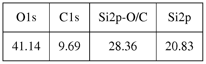
  • Figure 2 shows the X-ray photoelectron spectroscopy depth profile of the SiOC film.
  • Table 1 below shows the average elemental content in the bulk film.
  • a SiOC was deposited using according to the methods of Example 1 over a photoresist, silicon substrate with features, and blanket Si(100). Transmission electron microscope photographs of the films were taken and are shown in Figures 3-5, respectively. Figures 3-5 also show measurements of the film thickness at various points of the films. As can be seen in the photographs, the deposited films are very conformal over a variety of substrates, even over features in the substrate.

Landscapes

  • Chemical & Material Sciences (AREA)
  • Organic Chemistry (AREA)
  • General Chemical & Material Sciences (AREA)
  • Chemical Kinetics & Catalysis (AREA)
  • Engineering & Computer Science (AREA)
  • Materials Engineering (AREA)
  • Mechanical Engineering (AREA)
  • Metallurgy (AREA)
  • Inorganic Chemistry (AREA)
  • Chemical Vapour Deposition (AREA)

Abstract

Provided are methods of for deposition of SiOC. Certain methods involve exposing a substrate surface to a first and second precursor in the presence of a catalyst comprising a neutral two electron donor base. The first precursor has formula (XyH3-ySi)zCH4-z, or (XyH3_ ySi)(CH2)n(SiXyH3-y), wherein X is a halogen, y has a value of between 1 and 3, and z has a value of between 1 and 3, and n has a value between 2 and 5. The second precursor comprises water or a compound containing carbon and at least two hydroxyl groups. Certain other methods relate to exposing a substrate surface to a first and second precursor in the presence of a catalyst comprising a neutral two electron donor base, the first precursor comprising SiX4 or X3Si-SiX3, wherein X is a halide, and the second precursor comprising carbon and at least two hydroxyl groups.

Description

CATALYTIC ATOMIC LAYER DEPOSITION OF FILMS COMPRISING SiOC TECHNICAL FIELD
[0001] The present invention relates generally to methods of depositing thin films. In particular, the invention relates to atomic layer deposition processes for the deposition of SiOC films.
BACKGROUND
[0002] Deposition of thin films on a substrate surface is an important process in a variety of industries including semiconductor processing, diffusion barrier coatings and dielectrics for magnetic read/write heads. In the semiconductor industry, in particular, miniaturization requires atomic level control of thin film deposition to produce conformal coatings on high aspect structures. One method for deposition of thin films with control and conformal deposition is atomic layer deposition (ALD), which employs sequential, surface reactions to form layers of precise thickness. Most ALD processes are based on binary reaction sequences which deposit a binary compound film. Because the surface reactions are sequential, the two gas phase reactants are not in contact, and possible gas phase reactions that may form and deposit particles are limited.
[0003] ALD has been used to deposit metals and metal compounds on substrate surfaces. A1203 deposition is an example of a typical ALD process illustrating the sequential and self-limiting reactions characteristic of ALD. A1203 ALD conventionally uses trimethylaluminum (TMA, often referred to as reaction "A" or the "A" precursor) and H20 (often referred to as the "B" reaction or the "B" precursor). In step A of the binary reaction, hydroxyl surface species react with vapor phase TMA to produce surface-bound A10A1(CH )2 and CH4 in the gas phase. This reaction is self-limited by the number of reactive sites on the surface. In step B of the binary reaction, A1CH3 of the surface-bound compound reacts with vapor phase H20 to produce AIOH bound to the surface and CH4 in the gas phase. This reaction is self-limited by the finite number of available reactive sites on surface-bound A10A1(CH3)2. Subsequent cycles of A and B, purging gas phase reaction products and unreacted vapor phase precursors between reactions and between reaction cycles, produces A1203 growth in an essentially linear fashion to obtain the desired film thickness. [0004] In order to facilitate deposition, catalysts have been used during some ALD processes. The catalyst is used to activate a reaction between two or more species during the deposition process. One process involving catalytic ALD involves the deposition of Si02 using water and SiCl4. However, new catalytic ALD methods for other films are desired. SUMMARY
[0005] One aspect of the invention relates to a method of depositing a film. The method comprises exposing a substrate surface to a first and second precursor in the presence of a catalyst comprising a neutral two electron donor base, the first precursor having a formula (XyH3_ySi)zCH4_z or (XyH _ySi)(CH2)n(SiXyH _y), wherein X is a halogen, y has a value of between 1 and 3, and z has a value of between 1 and 3, and n has a value between 2 and 5, and the second precursor comprising water or a compound containing carbon and at least two hydroxyl groups. In one or more embodiments, each X is independently selected from CI, Br and I.
[0006] In some embodiments, the first precursor has a formula (XyH _ySi)zCH4_z. In further embodiments, the first precursor has a structure represented by:
Figure imgf000003_0001
Figure imgf000003_0002
or
In some embodiments, the first precursor comprises bis(trichlorosilyl)methane. In one or more embodiments, the first precursor has a formula (XyH3_ySi)(CH2)n(SiXyH3_y). In further embodiments, n has a value of 2 or 3.
[0007] In some embodiments, the catalyst comprises an amine. In one or more embodiments, the catalyst comprises pyridine or NH . In some embodiments, the second precursor comprises a diol. In one or more embodiments, the diol comprises ethylene glycol, propylene glycol and butane- 1,4-diol. In some embodiments, a film comprising SiOC is provided. [0008] Another aspect of the invention relates to a method of depositing a film, the method comprising exposing a substrate surface to a first and second precursor in the presence of a catalyst comprising a neutral two electron donor base, the first precursor comprising SiX4 or X3Si-SiX3, wherein X is a halide, and the second precursor comprises a compound containing carbon and at least two hydroxyl groups to provide a film comprising SiOC. In one or more embodiments, X is selected from the group consisting of CI, Br and I.
[0009] In some embodiments, the first precursor comprising SiX4. In one or more embodiments, the catalyst comprises an amine. In some embodiments, the catalyst comprises pyridine or NH3. In one or more embodiments, the second precursor is a diol. In some embodiments, the diol comprises ethylene glycol, propylene glycol and butane- 1,4-diol.
[0010] A third aspect of the invention relates to a method of depositing a film, the method comprising exposing a substrate surface to a first and second precursor in the presence of a catalyst comprising an pyridine, the first precursor comprising bis(trichlorosilyl)methane and the second precursor comprising water. BRIEF DESCRIPTION OF THE DRAWINGS
[0011] So that the manner in which the above recited features of the present invention can be understood in detail, a more particular description of the invention, briefly summarized above, may be had by reference to embodiments, some of which are illustrated in the appended drawings. It is to be noted, however, that the appended drawings illustrate only typical embodiments of this invention and are therefore not to be considered limiting of its scope, for the invention may admit to other equally effective embodiments.
[0012] FIG. shows an exemplary pulse sequence according to one or more embodiments of the invention;
[0013] FIG. 2 shows a depth profile of the elemental content of a film deposited according to one or more embodiments of the invention;
[0014] FIG. 3 shows a transmission electron microscope image of a film deposited according to one or more embodiments of the invention over a photoresist substrate;
[0015] FIG 4 shows a transmission electron microscope image of a film deposited according to one or more embodiments of the invention over a silicon substrate; and [0016] FIG 5 shows a transmission electron microscope image of a film deposited according to one or more embodiments of the invention over blanket Si(100).
DETAILED DESCRIPTION
[0017] Before describing several exemplary embodiments of the invention, it is to be understood that the invention is not limited to the details of construction or process steps set forth in the following description. The invention is capable of other embodiments and of being practiced or being carried out in various ways. It is also to be understood that the complexes and ligands of the present invention may be illustrated herein using structural formulas which have a particular stereochemistry. These illustrations are intended as examples only and are not to be construed as limiting the disclosed structure to any particular stereochemistry. Rather, the illustrated structures are intended to encompass all such complexes and ligands having the indicated chemical formula.
[0018] A "substrate" as used herein, refers to any substrate or material surface formed on a substrate upon which film processing is performed during a fabrication process. For example, a substrate surface on which processing can be performed include materials such as silicon, silicon oxide, strained silicon, silicon on insulator (SOI), carbon doped silicon oxides, silicon nitride, doped silicon, germanium, gallium arsenide, glass, sapphire, and any other materials such as metals, metal nitrides, metal alloys, and other conductive materials, depending on the application. Substrates include, without limitation, semiconductor wafers. Substrates may be exposed to a pretreatment process to polish, etch, reduce, oxidize, hydroxylate, anneal and/or bake the substrate surface. In addition to film processing directly on the surface of the substrate itself, in the present invention any of the film processing steps disclosed may also be performed on an underlayer formed on the substrate as disclosed in more detail below, and the term "substrate surface" is intended to include such underlayer as the context indicates.
[0019] It has been discovered that SiOC films can be deposited using certain silicon precursors which contain a halogen and a second precursor selected from water or a diol. Either the diol or silicon precursor may contain carbon, which ends up incorporated into the film. Such SiOC films can exhibit better dielectric constants than the conventional Si02 films. Specifically, the carbon content can lower the dielectric constant, which lowers leakage at a transistor level. [0020] Accordingly, one aspect of the invention relates to method of depositing a film.
The method comprises exposing a substrate surface to a first and second precursor in the presence of a catalyst comprising a neutral two electron donor base, the first precursor having a formula (XyH3_ySi)zCH4_z, or (XyH3_ySi)(CH2)n(SiXyH3_y), wherein X is a halogen, y has a value of between 1 and 3, and z has a value of between 1 and 3, and n has a value between 2 and 5, and the second precursor comprising water or a compound containing carbon and at least two hydroxyl groups. In one or more embodiments, a film comprising SiOC is provided.
[0021] The first precursor is a silicon precursor, and can act as both a silicon and carbon source. In some embodiments, the first precursor has a formula (XyH3_ySi)zCH4_z. In one or more embodiments, each X is independently selected from CI, Br and I. In further embodiments, embodiments at least one of the X groups is CI. In even further embodiments, all X groups are CI. Such a compound is known as bis(trichlorosilyl)methane, hexachlorodisilylmethylene, 1,1' -methylenebis( 1 ,1,1 -trichlorosilane), or methylenebis(trichlorosilane), and has a structure represented by:
CLSi · SiCI
Other examples of suitable precursors include, but are not limited to those having a structure represented by:
H H
SiCI, \ ^SiCI,H
HC Sr SiC H CI3S | \ HCI2Si \
SiC¼ SiCI2H
or
[0022] In other embodiments, the first precursor has a formula (XyH3_ ySi)(CH2)n(SiXyH3_y). In further embodiments, n has a value of 2 or 3, or in even further embodiments, 2. Compounds of this formula may be used to further increase the carbon content, as the starting C:Si ratio will be higher. In one or more embodiments, each X is independently selected from CI, Br and I. In further embodiments, embodiments at least one of the X groups is CI. In even further embodiments, all X groups are CI. [0023] In some embodiments, the second precursor may comprise water. In embodiments where the second precursor comprises water, the resulting film will still contain carbon from the first precursor.
[0024] In other embodiments, the second precursor comprises a compound containing carbon and at least two hydroxyl groups. In further embodiments, the second precursor comprises a diol. In even further embodiments, diols may be used which contain carbon. In such embodiments, carbon incorporated into the film may come from both the first and second precursors. Suitable second precursors, include, but are not limited to, ethylene glycol, propylene glycol and butane- 1,4-diol. In further embodiments, the diol comprises ethylene glycol. While not wishing to be bound to any particular theory, it is thought that at least two hydroxyl groups are necessary in order to allow for subsequent deposition cycles. That is, one OH group is used to deposit the second precursor, and then the second may be used for the next cycle to react with the Si-Cl in the first precursor. Films deposited using diols are thought to also have the advantage of being oxygen deficient. [0025] Various first and second precursors can be selected to tune the amount of carbon in the deposited film. The higher the carbon: silicon ratio of the precursors, the higher the ratio will be in the resulting SiOC film. For example, in embodiments where the first precursor has formula (XyH3_ySi)(CH2)n(SiXyH3_y), longer carbon chains can be selected to result in a higher carbon content in the deposited film. In one or more embodiments, the carbon content of the film is about 10%.
[0026] The catalyst comprises a neutral two electron donor base. In one or more embodiments, the catalyst comprises an amine. In further embodiments, the catalyst comprises a tertiary amine. In further embodiments, the catalyst comprises pyridine. In other embodiments, the catalyst comprises NH3. In embodiments relating to SiOC depositions at a temperature greater than 100 °C, a tertiary amine with a vapor pressure lower than pyridine (which is less than about 20 torr at 20 °C) can be used.
[0027] In an exemplary embodiment, the method comprises exposing a substrate surface to a first and second precursor in the presence of a catalyst comprising an amine, the first precursor comprising bis(trichlorosilyl)methane and the second precursor comprising water. In further embodiments, the catalyst comprises pyridine. In one or more embodiments, a film comprising SiOC is provided. [0028] Another aspect of the invention relates to a method of depositing a film, the method comprising a substrate surface to a first and second precursor in the presence of a catalyst comprising a neutral two electron donor base, the first precursor comprising SiX4 or X3Si-SiX3, wherein X is a halide, and the second precursor comprising a compound containing carbon and at least two diols.
[0029] Again, the first precursor is a silicon precursor. In some embodiments, the first precursor comprises SiX4. In other embodiments, the first precursor comprises X3Si-SiX3. In one or more embodiments, each X is independently selected from CI, Br and I. In further embodiments, embodiments at least one of the X groups is CI. In even further embodiments, all X groups are CI. In embodiments where the first precursor comprises X Si-SiX3, and all X groups are chlorine, the compound is Cl3Si-SiCl3, also known as hexachlorodisilane. Accordingly, in one or more embodiments, the silicon precursor is selected from SiCl4, SiBr4, or S1I4.
[0030] The second precursor comprises carbon and at least two hydroxyl groups. Carbon may be incorporated into the deposited film from the second precursor. Accordingly, in one or more embodiments, the resulting film comprises SiOC. In some embodiments, the second precursor may comprise a diol. Suitable second precursors, include, but are not limited to, ethylene glycol, propylene glycol and butane- 1,4-diol. In further embodiments, the diol comprises ethylene glycol. Again, as discussed above, it is thought that at least two OH groups are needed to repeat the cycle and get additional deposition.
[0031] The catalyst comprises a neutral two electron donor base. In one or more embodiments, the catalyst comprises an amine. In further embodiments, the catalyst comprises a tertiary amine. In further embodiments, the catalyst comprises pyridine. In other embodiments, the catalyst comprises NH3. In embodiments relating to SiOC depositions at a temperature greater than 100 °C, a tertiary amine with a vapor pressure lower than pyridine (which is less than about 20 torr at 20 °C) can be used.
[0032] The precursors may be flowed and/or exposed to the substrate surface either sequentially or substantially simultaneously. In embodiments where the substrate is exposed to the precursors sequentially, the process may be repeated up until a desired film thickness has been achieved. As used herein, "substantially simultaneously" refers to either co-flow or where there is merely overlap between exposures of the precursors. In one or more embodiments, the catalyst is added with any one or more of the reactants. In other embodiments, the catalyst is added alone, before and/or after any of the precursors.
[0033] The reaction conditions for the ALD reaction will be selected based on the properties of the film precursors, substrate surface, and the catalyst. The deposition may be carried out at atmospheric pressure, but may also be carried out at reduced pressure. The vapor pressure of the catalyst should be low enough to be practical in such applications. The substrate temperature should be low enough to keep the bonds of the substrate surface intact and to prevent thermal decomposition of gaseous reactants. However, the substrate temperature should also be high enough to keep the film precursors in the gaseous phase and to provide sufficient energy for surface reactions. The specific temperature depends on the specific substrate, film precursors, and catalyst used and pressure. The properties of the specific substrate, film precursors, and catalyst may be evaluated using methods known in the art, allowing selection of appropriate temperature and pressure for the reaction.
[0034] In one or more embodiments, the deposition is carried out at a temperature less than about 400, 350, 300, 250, 200, 150, 125, or 100 °C. In some embodiments, the deposition is carried out at a temperature in the range of about 70 to about 100 °C, about 70 to about 125 °C or about 70 to about 125 °C.
[0035] According to one or more embodiments, the substrate is subjected to processing prior to and/or after forming the layer. This processing can be performed in the same chamber or in one or more separate processing chambers. In some embodiments, the substrate is moved from the first chamber to a separate, second chamber for further processing. The substrate can be moved directly from the first chamber to the separate processing chamber, or it can be moved from the first chamber to one or more transfer chambers, and then moved to the desired separate processing chamber. Accordingly, the processing apparatus may comprise multiple chambers in communication with a transfer station. An apparatus of this sort may be referred to as a "cluster tool" or "clustered system," and the like.
[0036] Generally, a cluster tool is a modular system comprising multiple chambers which perform various functions including substrate center-finding and orientation, degassing, annealing, deposition and/or etching. According to one or more embodiments, a cluster tool includes at least a first chamber and a central transfer chamber. The central transfer chamber may house a robot that can shuttle substrates between and among processing chambers and load lock chambers. The transfer chamber is typically maintained at a vacuum condition and provides an intermediate stage for shuttling substrates from one chamber to another and/or to a load lock chamber positioned at a front end of the cluster tool. Two well-known cluster tools which may be adapted for the present invention are the Centura® and the Endura®, both available from Applied Materials, Inc., of Santa Clara, Calif. The details of one such staged- vacuum substrate processing apparatus is disclosed in U.S. Pat. No. 5,186,718, entitled "Staged- Vacuum Wafer Processing Apparatus and Method," Tepman et al., issued on Feb. 16, 1993. However, the exact arrangement and combination of chambers may be altered for purposes of performing specific steps of a process as described herein. Other processing chambers which may be used include, but are not limited to, cyclical layer deposition (CLD), atomic layer deposition (ALD), chemical vapor deposition (CVD), physical vapor deposition (PVD), etch, pre-clean, chemical clean, thermal treatment such as RTP, plasma nitridation, degas, orientation, hydroxylation and other substrate processes. By carrying out processes in a chamber on a cluster tool, surface contamination of the substrate with atmospheric impurities can be avoided without oxidation prior to depositing a subsequent film.
[0037] According to one or more embodiments, the substrate is continuously under vacuum or "load lock" conditions, and is not exposed to ambient air when being moved from one chamber to the next. The transfer chambers are thus under vacuum and are "pumped down" under vacuum pressure. Inert gases may be present in the processing chambers or the transfer chambers. In some embodiments, an inert gas is used as a purge gas to remove some or all of the reactants. According to one or more embodiments, a purge gas is injected at the exit of the deposition chamber to prevent reactants from moving from the deposition chamber to the transfer chamber and/or additional processing chamber. Thus, the flow of inert gas forms a curtain at the exit of the chamber.
[0038] The substrate can be processed in single substrate deposition chambers, where a single substrate is loaded, processed and unloaded before another substrate is processed. The substrate can also be processed in a continuous manner, like a conveyer system, in which multiple substrate are individually loaded into a first part of the chamber, move through the chamber and are unloaded from a second part of the chamber. The shape of the chamber and associated conveyer system can form a straight path or curved path. Additionally, the processing chamber may be a carousel in which multiple substrates are moved about a central axis and are exposed to deposition, etch, annealing, cleaning, etc. processes throughout the carousel path. [0039] During processing, the substrate can be heated or cooled. Such heating or cooling can be accomplished by any suitable means including, but not limited to, changing the temperature of the substrate support and flowing heated or cooled gases to the substrate surface. In some embodiments, the substrate support includes a heater/cooler which can be controlled to change the substrate temperature conductively. In one or more embodiments, the gases (either reactive gases or inert gases) being employed are heated or cooled to locally change the substrate temperature. In some embodiments, a heater/cooler is positioned within the chamber adjacent the substrate surface to convectively change the substrate temperature.
[0040] The substrate can also be stationary or rotated during processing. A rotating substrate can be rotated continuously or in discreet steps. For example, a substrate may be rotated throughout the entire process, or the substrate can be rotated by a small amount between exposure to different reactive or purge gases. Rotating the substrate during processing (either continuously or in steps) may help produce a more uniform deposition or etch by minimizing the effect of, for example, local variability in gas flow geometries. [0041] Reference throughout this specification to "one embodiment," "certain embodiments," "one or more embodiments" or "an embodiment" means that a particular feature, structure, material, or characteristic described in connection with the embodiment is included in at least one embodiment of the invention. Thus, the appearances of the phrases such as "in one or more embodiments," "in certain embodiments," "in one embodiment" or "in an embodiment" in various places throughout this specification are not necessarily referring to the same embodiment of the invention. Furthermore, the particular features, structures, materials, or characteristics may be combined in any suitable manner in one or more embodiments.
[0042] Although the invention herein has been described with reference to particular embodiments, it is to be understood that these embodiments are merely illustrative of the principles and applications of the present invention. It will be apparent to those skilled in the art that various modifications and variations can be made to the method and apparatus of the present invention without departing from the spirit and scope of the invention. Thus, it is intended that the present invention include modifications and variations that are within the scope of the appended claims and their equivalents.
EXAMPLES Example 1
[0043] A SiOC was deposited using hexachlorodisilylmethylene and water using a pyridine catalyst. The pressure and temperature of the chamber were 12 torr and 70 °C, respectively. The pulse sequence is shown in Figure 1, which shows alternating pyridine/hexachlorodisilylmethylene pulses followed by alternating pyridine/water pulses. The hexachlorodisilylmethylene pulse length was 2.0 seconds, surrounded by a curtain of 1.0 second pyridine pulses. The water pulse length was 0.2 seconds, also surrounded by a curtain of 1.0 second pyridine pulses. Purge length was 10 seconds. The cycle was repeated 150 times to arrive at a film thickness of 16.7nm, corresponding to 1.1 Angstroms growth per cycle.
Example 2
[0044] A SiOC was deposited using according to the methods of Example 1, except that the deposition was carried out to a film thickness of about 60-70 Angstroms. Figure 2 shows the X-ray photoelectron spectroscopy depth profile of the SiOC film. Table 1 below shows the average elemental content in the bulk film.
Table 1 : Average Content in Bulk Film
Figure imgf000012_0001
[0045] As seen from Table 1 and Figure 2, no nitrogen or chlorine ends up deposited, showing that the precursor does not contaminate the film. The resulting carbon content was around 10%.
Examples 3-5
[0046] A SiOC was deposited using according to the methods of Example 1 over a photoresist, silicon substrate with features, and blanket Si(100). Transmission electron microscope photographs of the films were taken and are shown in Figures 3-5, respectively. Figures 3-5 also show measurements of the film thickness at various points of the films. As can be seen in the photographs, the deposited films are very conformal over a variety of substrates, even over features in the substrate.
Claims

What is claimed is:
1. A method of depositing a film, the method comprising exposing a substrate surface to a first and second precursor in the presence of a catalyst comprising a neutral two electron donor base, the first precursor having a formula (XyH3_ySi)zCH4_z or (XyH _ ySi)(CH2)n(SiXyH3_y), wherein each X is independently selected from CI, Br and I, y has a value of between 1 and 3, and z has a value of between 1 and 3, and n has a value between 2 and 5, and the second precursor comprising water or a compound containing carbon and at least two hydroxyl groups.
2. The method of claim 1, wherein the first precursor has a formula (XyH3_ySi)zCH4_z.
3. The method of claim 1 or 2, wherein the first precursor has a structure represented by:
Figure imgf000014_0001
H
SiCI ,
cusr HC Si \ -SiCI,H
SiCI,H
or
4. The method of any of claims 1-3, wherein the first precursor comprises bis (trichloro silyl)methane .
5. The method of any of claims 1-4, wherein the first precursor has a formula (XyH _ ySi)(CH2)n(SiXyH3_y).
6. The method of any of claims 1-5, wherein n has a value of 2 or 3.
7. The method of any of claims 1-6, wherein the catalyst comprises an amine, pyridine or NH3.
8. The method of any of claims 1-7, wherein the second precursor comprises a diol.
9. The method of any of claims 1-8, wherein the diol comprises ethylene glycol, propylene glycol and butane- 1,4-diol.
10. The method of any of claims 1-9, wherein a film comprising SiOC is provided.
11. A method of depositing a film, the method comprising exposing a substrate surface to a first and second precursor in the presence of a catalyst comprising a neutral two electron donor base, the first precursor comprising SiX4 or X3Si-SiX3, wherein each X is independently selected from CI, Br and I, and the second precursor comprises a compound containing carbon and at least two hydroxyl groups to provide a film comprising SiOC.
12. The method of claim 11, wherein the first precursor comprising SiX4.
13. The method of claim 11 or 12, wherein the catalyst comprises an amine, pyridine or NH3.
14. The method of any of claims 11-13, wherein the second precursor is a diol.
15. The method of any of claims 11-14, wherein the diol comprises ethylene glycol, propylene glycol and butane- 1,4-diol.
PCT/US2014/017391 2013-02-22 2014-02-20 Catalytic atomic layer deposition of films comprising sioc Ceased WO2014130668A1 (en)

Priority Applications (2)

Application Number Priority Date Filing Date Title
US14/769,722 US20160002782A1 (en) 2013-02-22 2014-02-20 Catalytic Atomic Layer Deposition Of Films Comprising SiOC
KR1020157025636A KR20150125674A (en) 2013-02-22 2014-02-20 CATALYTIC ATOMIC LAYER DEPOSITION OF FILMS COMPRISING SiOC

Applications Claiming Priority (2)

Application Number Priority Date Filing Date Title
US201361767860P 2013-02-22 2013-02-22
US61/767,860 2013-02-22

Publications (1)

Publication Number Publication Date
WO2014130668A1 true WO2014130668A1 (en) 2014-08-28

Family

ID=51391804

Family Applications (1)

Application Number Title Priority Date Filing Date
PCT/US2014/017391 Ceased WO2014130668A1 (en) 2013-02-22 2014-02-20 Catalytic atomic layer deposition of films comprising sioc

Country Status (4)

Country Link
US (1) US20160002782A1 (en)
KR (1) KR20150125674A (en)
TW (1) TW201435132A (en)
WO (1) WO2014130668A1 (en)

Cited By (1)

* Cited by examiner, † Cited by third party
Publication number Priority date Publication date Assignee Title
US11049807B2 (en) 2019-09-25 2021-06-29 Sandisk Technologies Llc Three-dimensional memory device containing tubular blocking dielectric spacers

Families Citing this family (3)

* Cited by examiner, † Cited by third party
Publication number Priority date Publication date Assignee Title
DE102018110837A1 (en) 2017-09-29 2019-04-04 Taiwan Semiconductor Manufacturing Co., Ltd. Processes for forming features with a low K value and constructions formed thereby
US10304677B2 (en) * 2017-09-29 2019-05-28 Taiwan Semiconductor Manufacturing Co., Ltd. Low-k feature formation processes and structures formed thereby
US12438050B2 (en) * 2023-02-14 2025-10-07 Applied Materials, Inc. Electronic device fabrication using area-selective deposition

Citations (5)

* Cited by examiner, † Cited by third party
Publication number Priority date Publication date Assignee Title
KR20010104285A (en) * 2000-05-12 2001-11-24 마찌다 가쯔히꼬 Method of forming a carbon silicon oxide
EP1925692A1 (en) * 2006-11-14 2008-05-28 Applied Materials, Inc. Method of depositing hafnium silicate by catalyst assisted atomic layer deposition
US20090081883A1 (en) * 2007-09-26 2009-03-26 Freeman Diane C Process for depositing organic materials
US20120052681A1 (en) * 2010-08-31 2012-03-01 Micron Technology, Inc. Methods of selectively forming a material
US20120276306A1 (en) * 2011-04-26 2012-11-01 Asm Japan K.K. Atomic Layer Deposition For Controlling Vertical Film Growth

Family Cites Families (4)

* Cited by examiner, † Cited by third party
Publication number Priority date Publication date Assignee Title
JP5110239B2 (en) * 2004-05-11 2012-12-26 Jsr株式会社 Method for forming organic silica film, composition for film formation
US20060228903A1 (en) * 2005-03-30 2006-10-12 Mcswiney Michael L Precursors for the deposition of carbon-doped silicon nitride or silicon oxynitride films
JP2011091362A (en) * 2009-09-28 2011-05-06 Hitachi Kokusai Electric Inc Method of manufacturing semiconductor device, and substrate processing apparatus
US8685867B1 (en) * 2010-12-09 2014-04-01 Novellus Systems, Inc. Premetal dielectric integration process

Patent Citations (5)

* Cited by examiner, † Cited by third party
Publication number Priority date Publication date Assignee Title
KR20010104285A (en) * 2000-05-12 2001-11-24 마찌다 가쯔히꼬 Method of forming a carbon silicon oxide
EP1925692A1 (en) * 2006-11-14 2008-05-28 Applied Materials, Inc. Method of depositing hafnium silicate by catalyst assisted atomic layer deposition
US20090081883A1 (en) * 2007-09-26 2009-03-26 Freeman Diane C Process for depositing organic materials
US20120052681A1 (en) * 2010-08-31 2012-03-01 Micron Technology, Inc. Methods of selectively forming a material
US20120276306A1 (en) * 2011-04-26 2012-11-01 Asm Japan K.K. Atomic Layer Deposition For Controlling Vertical Film Growth

Cited By (1)

* Cited by examiner, † Cited by third party
Publication number Priority date Publication date Assignee Title
US11049807B2 (en) 2019-09-25 2021-06-29 Sandisk Technologies Llc Three-dimensional memory device containing tubular blocking dielectric spacers

Also Published As

Publication number Publication date
TW201435132A (en) 2014-09-16
US20160002782A1 (en) 2016-01-07
KR20150125674A (en) 2015-11-09

Similar Documents

Publication Publication Date Title
US20230090196A1 (en) Methods For Atomic Layer Deposition Of SiCO(N) Using Halogenated Silylamides
US9643844B2 (en) Low temperature atomic layer deposition of films comprising SiCN or SiCON
US20220172989A1 (en) Nucleation-Free Gap Fill ALD Process
US11702742B2 (en) Methods of forming nucleation layers with halogenated silanes
US11028478B2 (en) Atomic layer deposition of films comprising silicon, carbon and nitrogen using halogenated silicon precursors
KR102298038B1 (en) Methods of depositing a metal alloy film
US9685325B2 (en) Carbon and/or nitrogen incorporation in silicon based films using silicon precursors with organic co-reactants by PE-ALD
US10147599B2 (en) Methods for depositing low K and low wet etch rate dielectric thin films
KR20220118521A (en) Silicon carbonitride gapfill with tunable carbon content
CN117425746B (en) Method for reducing deposition rate
US20160002782A1 (en) Catalytic Atomic Layer Deposition Of Films Comprising SiOC
US9982345B2 (en) Deposition of metal films using beta-hydrogen free precursors
US20160307748A1 (en) Deposition Of Si-H Free Silicon Nitride
US9200365B2 (en) Method of catalytic film deposition
WO2014152826A1 (en) Deposition of films using disiloxane precursors
US10323054B2 (en) Precursors for deposition of metal, metal nitride and metal oxide based films of transition metals
WO2021055761A1 (en) Methods for atomic layer deposition of sico(n) using halogenated silylamides

Legal Events

Date Code Title Description
121 Ep: the epo has been informed by wipo that ep was designated in this application

Ref document number: 14753992

Country of ref document: EP

Kind code of ref document: A1

WWE Wipo information: entry into national phase

Ref document number: 14769722

Country of ref document: US

NENP Non-entry into the national phase

Ref country code: DE

ENP Entry into the national phase

Ref document number: 20157025636

Country of ref document: KR

Kind code of ref document: A

122 Ep: pct application non-entry in european phase

Ref document number: 14753992

Country of ref document: EP

Kind code of ref document: A1