WO2014123046A1 - Gate driving circuit - Google Patents
Gate driving circuit Download PDFInfo
- Publication number
- WO2014123046A1 WO2014123046A1 PCT/JP2014/051948 JP2014051948W WO2014123046A1 WO 2014123046 A1 WO2014123046 A1 WO 2014123046A1 JP 2014051948 W JP2014051948 W JP 2014051948W WO 2014123046 A1 WO2014123046 A1 WO 2014123046A1
- Authority
- WO
- WIPO (PCT)
- Prior art keywords
- current
- switching element
- gate
- circuit
- voltage
- Prior art date
Links
Images


Classifications
-
- H—ELECTRICITY
- H03—ELECTRONIC CIRCUITRY
- H03K—PULSE TECHNIQUE
- H03K17/00—Electronic switching or gating, i.e. not by contact-making and –breaking
- H03K17/14—Modifications for compensating variations of physical values, e.g. of temperature
- H03K17/145—Modifications for compensating variations of physical values, e.g. of temperature in field-effect transistor switches
-
- H—ELECTRICITY
- H03—ELECTRONIC CIRCUITRY
- H03K—PULSE TECHNIQUE
- H03K17/00—Electronic switching or gating, i.e. not by contact-making and –breaking
- H03K17/08—Modifications for protecting switching circuit against overcurrent or overvoltage
- H03K17/082—Modifications for protecting switching circuit against overcurrent or overvoltage by feedback from the output to the control circuit
- H03K17/0828—Modifications for protecting switching circuit against overcurrent or overvoltage by feedback from the output to the control circuit in composite switches
-
- H—ELECTRICITY
- H03—ELECTRONIC CIRCUITRY
- H03K—PULSE TECHNIQUE
- H03K17/00—Electronic switching or gating, i.e. not by contact-making and –breaking
- H03K17/14—Modifications for compensating variations of physical values, e.g. of temperature
-
- H—ELECTRICITY
- H03—ELECTRONIC CIRCUITRY
- H03K—PULSE TECHNIQUE
- H03K17/00—Electronic switching or gating, i.e. not by contact-making and –breaking
- H03K17/16—Modifications for eliminating interference voltages or currents
- H03K17/161—Modifications for eliminating interference voltages or currents in field-effect transistor switches
-
- H—ELECTRICITY
- H03—ELECTRONIC CIRCUITRY
- H03K—PULSE TECHNIQUE
- H03K17/00—Electronic switching or gating, i.e. not by contact-making and –breaking
- H03K17/08—Modifications for protecting switching circuit against overcurrent or overvoltage
- H03K2017/0806—Modifications for protecting switching circuit against overcurrent or overvoltage against excessive temperature
Definitions
- the present invention relates to a gate drive circuit for driving a semiconductor switching element as a power conversion semiconductor element.
- the switching element is controlled by controlling the gate resistance and the gate voltage according to the driving conditions (for example, current value and temperature). It is necessary to adjust the value of the gate current for.
- a temperature detection in the vicinity of the switching element is performed, and when an abnormality is detected, a protective operation such as stopping the switching operation is performed.
- the switching loss can be reduced and the switching noise can be reduced, for example, due to a change in temperature in the vicinity of the switching element, the switching loss becomes too large and the element is destroyed, or excessive switching noise is generated. was difficult.
- the present invention has been made to solve the above-described problems, and is capable of performing control to adjust the gate current to the switching element in accordance with changes in temperature conditions when the switching element is driven, and automatically. It is another object of the present invention to provide a gate drive circuit that can achieve both reduction in switching loss and reduction in switching noise.
- a gate drive circuit drives the switching element by charging and discharging a gate electrode of the switching element for power conversion, and includes a temperature detection circuit for detecting the temperature of the switching element, and the temperature A current source for flowing a forward current to the detection circuit; an amplifier circuit for amplifying the forward voltage of the temperature detection circuit; and a magnitude of the gate current to be passed to the gate electrode of the switching element based on the output voltage of the amplification circuit.
- the switching current of the switching element is controlled so as to decrease, thereby reducing the switching speed of the switching element. Suppresses the generation of switching noise.
- control is performed so that the gate current of the switching element increases, and the switching speed of the switching element is increased to suppress the increase in switching loss. Can do.
- both switching loss and switching noise can be automatically reduced, and a temperature detection circuit and a current adjustment circuit for adjusting the gate current can be realized with a smaller number of elements than in the past, and the gate can be realized.
- the current value can be adjusted with high accuracy.
- FIG. 1 is a circuit diagram showing a gate drive circuit according to a first embodiment of the present invention.
- FIG. 5 is a characteristic diagram showing a voltage-current relationship of a diode constituting the temperature detection circuit of the gate drive circuit according to the first embodiment of the present invention. It is a characteristic view which shows the temperature dependence of the input voltage and output voltage of the amplifier circuit of the gate drive circuit by Embodiment 1 of this invention. It is a characteristic view which shows the switching time with respect to the gate resistance of a switching element, and the relationship of switching loss.
- It is a circuit diagram which shows the gate drive circuit by Embodiment 2 of this invention.
- Embodiment 3 of this invention It is a circuit diagram which shows the gate drive circuit by Embodiment 4 of this invention.
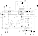
- FIG. 1 is a circuit diagram showing a gate drive circuit according to Embodiment 1 of the present invention.
- the gate drive circuit according to the first embodiment includes a power conversion switching element 1 made of, for example, an IGBT (Insulated Gate Bipolar Transistor) that constitutes a converter or an inverter. 2 is connected.
- the switching element 1 is not limited to an IGBT, and a semiconductor element such as a power MOSFET (Metal Oxide Semiconductor Field Effect Transistor), a bipolar transistor, or a GTO (Gate Turn Off thyristor) can be used.
- a power MOSFET Metal Oxide Semiconductor Field Effect Transistor
- bipolar transistor Bipolar transistor
- GTO Gate Turn Off thyristor
- a temperature detection circuit 4 formed by connecting a plurality of diodes 3 in series is provided at a close position where a temperature difference hardly occurs on the same chip on which the switching element 1 and the diode 2 are formed.
- One end side of the temperature detection circuit 4 is connected to the control power source 5 via a current limiting resistor R 1, and the other end side is connected to the ground side terminal 13.
- the control power source 5 corresponds to a current source that sends a forward current to the temperature detection circuit 4 in the claims.
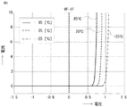
- the output characteristics of the diode 3 constituting the temperature detection circuit 4 are as shown in FIG. Therefore, the temperature of the switching element 1 can be detected by the temperature detection circuit 4 by acquiring the temperature dependence of the voltage-current characteristics of the diode 3 as shown in FIG.
- a control power source 5 On the gate side of the switching element 1, a control power source 5, a current limiting resistor R2, a P-channel type MOSFET 7 for charging the gate electrode of the switching element 1 by flowing a gate current, a current limiting resistor R3, and N-channel MOSFETs 8 for stopping and discharging the gate current to the gate electrode of the switching element 1 are sequentially connected, and the source side of the MOSFET 8 is connected to the ground side terminal 13. Note that the voltage Vcc of the control power supply 5 is adjusted to a constant voltage in order to drive the switching element 1.
- One input terminal of the first operational amplifier 9 is connected to a connection point between the current limiting resistor R1 and the current input side of the temperature detection circuit 4.
- the other input terminal of the first operational amplifier 9 is connected to the ground side terminal 13 via a resistor R4.
- a Zener diode 10 is connected to the output terminal of the first operational amplifier 9.
- the resistor R5 is a feedback resistor for the first operational amplifier 9.
- the first operational amplifier 9 corresponds to an amplifier circuit that amplifies the forward voltage of the temperature detection circuit 4 in the claims.
- One input terminal of the second operational amplifier 12 is connected to a connection point between the current limiting resistor R2 and the drain of the MOSFET 7.
- a voltage adjusting resistor R6 is connected to the control power source 5, and the other input terminal of the second operational amplifier 12 is connected to a connection point between the resistor R6 and the Zener diode 10.
- the output terminal of the second operational amplifier 12 is connected to the gate of the MOSFET 7.
- the second operational amplifier 12 and the MOSFET 7 correspond to a current adjustment circuit that adjusts the magnitude of the gate current I flowing through the gate electrode of the switching element 1 in the claims.
- the input terminal 14 is an input terminal of a control signal input from the outside in order to turn on / off the switching element 1.
- the input terminal 14 is connected to the gate of the MOSFET 8 through the resistor R7, and is connected to a connection point between the resistor R6 and the Zener diode 10 through the resistor R8 and the diode 15.
- the two MOSFETs 7 and 8 correspond to a drive circuit that receives an external signal and turns on / off the switching element 1 in the claims.
- the forward voltage Va of the temperature detection circuit 4 is amplified by the first operational amplifier 9.
- the threshold voltage component Vz of the Zener diode 10 becomes an offset voltage of the output voltage after amplification of the first operational amplifier 9, and therefore, the voltage obtained by subtracting the offset voltage Vz is used for adjusting the gate current. Is used as the current adjustment voltage Vb.
- the current adjustment voltage Vb obtained by subtracting the offset voltage Vz has a characteristic that increases as the temperature decreases, as can be seen from the characteristic of FIG.
- an offset may be provided in the first operational amplifier 9 in addition to the above method.
- the forward voltage Va of the temperature detection circuit 4 increases, so that the first operational amplifier 9 has the same voltage difference between both input terminals of the first operational amplifier 9.
- the current adjustment voltage Vb is adjusted to be larger than the voltage obtained by dividing the potential Vcc of the control power supply 5 by the resistors R6 and R8.
- the potential difference between the current adjustment voltage Vb of the second operational amplifier 12 and the potential Vcc of the control power supply 5 becomes small, so the second operational amplifier 12 adjusts the gate voltage of the MOSFET 7 so that the on-resistance value becomes large. Therefore, the gate current I of the switching element 1 is controlled to decrease.
- the forward voltage Va of the temperature detection circuit 4 is small, so that the output voltage of the first operational amplifier 9 is adjusted to a lower voltage than when the temperature is low.
- the current adjustment voltage Vb is adjusted to be smaller than the voltage obtained by dividing the potential Vcc of the control power supply 5 by the resistors R6 and R8. Therefore, since the voltage difference between the two input terminals of the second operational amplifier 12 is greatly adjusted, the second operational amplifier 12 adjusts the gate voltage of the MOSFET 7 so that the on-resistance value becomes small.
- the gate current I is controlled to increase.
- the gate current I can be adjusted by changing the temperature of the switching element 1 by adjusting the gain of the first operational amplifier 9 or connecting a resistor (not shown) in series with the Zener diode 10. .
- the Zener diode 10 is configured to be disposed on the same chip as the switching element 1 here, but is not limited to this configuration, and may be disposed as a different chip. For example, it is good also as a structure arrange
- Zener diode 10 having a rating of 5 V or higher is used, the breakdown voltage increases as the temperature rises.
- the breakdown voltage of the Zener diode 10 is reduced at the same time, so that the current adjustment voltage Vb is adjusted to be increased.
- the current adjustment circuits 12 and 7 are controlled to reduce the gate current I to the switching element 1.
- the breakdown voltage of the Zener diode 10 increases at the same time, so that the current adjustment voltage Vb is adjusted to be small.
- the current adjustment circuits 12 and 7 are controlled to increase the gate current I for the switching element 1.
- the positive current zener diode 10 is used so that the gate current I of the switching element 1 increases as the ambient temperature rises.
- Zener diode 10 typically exhibits negative characteristics. Therefore, when the Zener diode 10 having such a negative characteristic is used, the breakdown voltage decreases as the temperature rises, so that the current adjustment voltage Vb increases. As a result, the current adjustment circuits 12 and 7 cause the switching element 1 to switch.
- the gate current I is controlled to be small. Thus, the correction tendency of the gate current I can be adjusted according to the characteristics of the Zener diode 10 to be used.
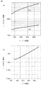
- FIG. 4A shows the relationship between the gate resistance of the switching element 1 and the switching time
- FIG. 4B shows the relationship between the gate resistance and the switching loss.
- the relationship between the gate resistance and the magnitude of the gate current is inversely proportional, and the gate current increases when the gate resistance is small.
- the gate resistance corresponds to the on-resistance of the MOSFET 7.
- the junction temperature of the switching element 1 does not reach the breakdown level even if the switching loss of the switching element 1 increases somewhat, so that the gate resistance of the switching element 1 is increased (that is, By reducing the switching time by decreasing the gate current I, the current change (di / dt) is reduced, and as a result, the generation of switching noise can be reduced.
- the relationship between the switching time of the switching element 1 and the magnitude of the switching noise is determined by the inductance value and the magnitude of the current determined by the shape of the circuit to which the switching element 1 is connected, but in any case,
- the gate resistance of the switching element 1 is reduced (that is, the gate current I is increased)
- the switching time is shortened, so that the switching loss is reduced, but the current change (di / dt) when the switching element 1 is turned on / off. ) Increases, resulting in increased switching noise.
- the temperature of the switching element 1 also varies depending on the conditions in which the switching element 1 is installed and the method such as cooling, but as the gate resistance increases (that is, when the gate current I decreases), the switching loss increases. The temperature of the element also tends to increase.
- the value of the on-resistance between the source and drain of the MOSFET 7 can be controlled by controlling the gate voltage of the MOSFET 7.
- the second operational amplifier 12 adjusts the on-resistance of the MOSFET 7 corresponding to the output impedance of the current adjustment circuit in accordance with the change in the temperature condition when the switching element 1 is driven. Then, by controlling the gate current I of the switching element 1, both reduction of switching loss and reduction of switching noise are automatically achieved.
- the gate voltage applied to the gate of the MOSFET 7 from the second operational amplifier 12 is lowered to reduce the on-resistance (gate resistance) of the MOSFET 7 from 10 ⁇ to 40 ⁇ .
- the switching time when the switching element 1 is turned on is changed from 25 ns to 43 ns, and the switching time when the switching element 1 is turned off is changed from 280 ns to 770 ns, thereby reducing noise generated during switching.
- the loss during switching increases from 1.2 mJ to 1.8 mJ.
- the gate current I of the switching element 1 decreases, and the switching speed of the switching element 1 is reduced. By slowing down, the generation of switching noise is suppressed. Further, when the switching element 1 is at a high temperature and the switching loss is unacceptable, the gate current I of the switching element 1 is controlled to increase and the switching speed of the switching element 1 is increased to increase the switching loss. Suppress.
- the switching loss of the switching element 1 can be automatically reduced and the switching noise can be reduced, so that the switching loss becomes too large due to the temperature change in the vicinity of the switching element 1 as in the prior art. Therefore, it is possible to eliminate problems such as device destruction and excessive switching noise.
- FIG. FIG. 5 is a circuit diagram showing a gate drive circuit according to the second embodiment of the present invention. Components corresponding to or corresponding to those of the first embodiment shown in FIG.
- the power supply voltage Vcc of the control power supply 5 may fluctuate due to temperature changes or noise from other circuits.
- the forward voltage Va of the temperature detection circuit 4 fluctuates accordingly, and the forward current of the diode 3 fluctuates.
- an accurate temperature change cannot be detected, and the temperature The driving state of the switching element 1 changes depending on other conditions.
- a constant current generator 17 is provided for supplying a constant current so that the magnitude of the forward current of the temperature detection circuit 4 is always constant. That is, the constant current generator 17 includes resistors R10 to R12 having a known resistance value, a third operational amplifier 18, and a P-channel type MOSFET 19 which is a semiconductor element for current adjustment.
- a resistor R10 and a MOSFET 19 constituting a constant current generator 17 are sequentially connected.
- One input terminal of the third operational amplifier 18 is connected to a connection point between the resistor R10 and the drain of the MOSFET 19.
- two resistors R11 and R12 constituting a constant current generator 17 are connected in series between the control power supply 5 and the ground side terminal 13, and the other end of the third operational amplifier 18 is connected to a connection point between the resistors R11 and R12. Are connected.
- the currents are set such that the voltage drops at the resistors R10 and R11 are the same with respect to the voltage Vcc of the control power supply 5, that is, the voltages applied to both input terminals of the third operational amplifier 18 are the same.
- the magnitude of the forward current flowing through the temperature detection circuit 4 is adjusted to be always constant.
- a filter 20 is provided in front of one input terminal of the first operational amplifier 9 to reduce the influence of noise from the outside. Thereby, stable operation can be realized. Since other configurations and operational effects are the same as those of the first embodiment, detailed description thereof is omitted here.
- FIG. 6 is a circuit diagram showing a gate drive circuit according to the third embodiment of the present invention. Components corresponding to or corresponding to those of the first embodiment shown in FIG.
- the third embodiment is different from the first embodiment in that it has an input terminal 21 for inputting the adjustment voltage Vd from the outside so that the gate current I of the switching element 1 can be controlled from the outside.
- the input terminal 21 is connected to the other input terminal of the second operational amplifier 12 via a voltage adjusting resistor R14.
- a voltage adjusting resistor R13 is connected to the output terminal of the first operational amplifier 9.
- the current adjustment voltage Vb based on the output voltage of the first operational amplifier 9 can be corrected by the adjustment voltage Vd input from the input terminal 21. Then, by adding the current adjustment voltage Vb corrected by the adjustment voltage Vd to the other input terminal of the second operational amplifier 12, the gate voltage applied from the second operational amplifier 12 to the MOSFET 7 is adjusted to adjust the switching element 1.
- the gate current I is controlled.
- the ratio of the change in the change can be adjusted by the resistors R13 and R14 and the gain of the first operational amplifier 9.
- the magnitude of the gate resistance when the switching element 1 is turned on is determined by the magnitude of the resistor R2 and the on-resistance of the MOSFET 7, and the magnitude of the gate resistance at the turn-off is determined by the magnitude of the resistor R3 and the on-resistance of the MOSFET 8. Determined. Therefore, the value of the resistor is adjusted in accordance with the characteristics of the driven switching element 1, and the switching element 1 depends on the temperature state of the switching element 1 and the magnitude of the adjustment voltage Vd input to the input terminal 21 from the outside.
- the gate current I can be adjusted. Since other configurations and operational effects are the same as those of the first embodiment, detailed description thereof is omitted here.
- FIG. 7 is a circuit diagram showing a gate drive circuit according to the fourth embodiment of the present invention. Components corresponding to or corresponding to those of the first embodiment shown in FIG.
- the fourth embodiment is different from the first embodiment in that a constant current diode 22 is provided between the control power supply 5 and the diode 3 of the temperature detection circuit 4 in order to adjust the current flowing through the temperature detection circuit 4. It has been.
- an input terminal 14 for a control signal input from the outside in order to turn on / off the switching element 1 is connected to the source side of the MOSFET 7 constituting the current adjustment circuit via a current limiting resistor R2. .
- a body diode of the MOSFET 7 may be used instead of connecting the off diode 20 in parallel with the MOSFET 7. Further, when the value of the current limiting resistor R2 is small, a resistor may be connected in series with the OFF diode 23 in series therewith.
- the correction tendency of the gate current I can be adjusted according to the positive / negative characteristics of the Zener diode 10 to be used, as described in the first embodiment.
- the Zener diode 10 may be disposed not only on the same chip as the switching element 1 but also as a separate chip. For example, you may arrange
- the switching speed can be automatically adjusted by varying the magnitude of the gate current I of the switching element 1 according to the chip temperature of the switching element 1 and the ambient temperature.
- the switching element 1 can be driven by automatically adjusting the trade-off between the switching noise and the switching loss based on the control signal applied to the input terminal 14 from the outside.
- Embodiments 1 to 4 are not limited to the configurations of Embodiments 1 to 4 described above, and various modifications can be made to the configurations of Embodiments 1 to 4 without departing from the spirit of the present invention. Alternatively, the configuration can be omitted, and the configurations of Embodiments 1 to 4 can be combined as appropriate.
- the semiconductor element such as the switching element 1 is formed of silicon.
- the present invention is not limited to this, and a wide band gap semiconductor material having a band gap larger than that of silicon is used. It may be formed. Examples of such a wide band gap semiconductor material include silicon carbide, a gallium nitride-based material, and diamond.
- a semiconductor element such as the switching element 1 formed of such a wide band gap semiconductor material has high voltage resistance and high allowable current density, and thus can be miniaturized. Then, by using these miniaturized switching elements 1 and the like, it is possible to miniaturize a semiconductor module incorporating these elements. Moreover, since heat resistance is also high, it is possible to reduce the size of the heat dissipating fins of the heat sink and the size of the water cooling part. Furthermore, since the power loss is low, it is possible to increase the efficiency of the switching element and the diode, and consequently increase the efficiency of the semiconductor module.
- the switching element 1 made of a wide band gap semiconductor material tends to generate more switching noise than the switching element made of silicon, and therefore it is particularly effective to apply the present invention. .
Abstract
Description
図1は、この発明の実施の形態1におけるゲート駆動回路を示す回路図である。
この実施の形態1のゲート駆動回路は、例えば、コンバータやインバータを構成するIGBT(Insulated Gate Bipolar Transistor)からなる電力変換用のスイッチング素子1を備え、このスイッチング素子1に逆並列に還流用のダイオード2が接続されている。なお、スイッチング素子1としては、IGBTに限らず、バワーMOSFET(Metal Oxide Semiconductor Field Effect Transistor)、バイポーラトランジスタ、GTO(Gate Turn Off thyristor)などの半導体素子を使用することができる。
1 is a circuit diagram showing a gate drive circuit according to
The gate drive circuit according to the first embodiment includes a power
図5はこの発明の実施の形態2におけるゲート駆動回路を示す回路図であり、図1に示した実施の形態1と対応もしくは相当する構成部分には同一の符号を付す。
FIG. 5 is a circuit diagram showing a gate drive circuit according to the second embodiment of the present invention. Components corresponding to or corresponding to those of the first embodiment shown in FIG.
その他の構成、および作用効果は実施の形態1と同様であるから、ここでは詳しい説明は省略する。 In the second embodiment, a
Since other configurations and operational effects are the same as those of the first embodiment, detailed description thereof is omitted here.
図6はこの発明の実施の形態3におけるゲート駆動回路を示す回路図であり、図1に示した実施の形態1と対応もしくは相当する構成部分には同一の符号を付す。
FIG. 6 is a circuit diagram showing a gate drive circuit according to the third embodiment of the present invention. Components corresponding to or corresponding to those of the first embodiment shown in FIG.
その他の構成、および作用効果は実施の形態1と同様であるから、ここでは詳しい説明は省略する。 That is, the magnitude of the gate resistance when the switching
Since other configurations and operational effects are the same as those of the first embodiment, detailed description thereof is omitted here.
図7はこの発明の実施の形態4におけるゲート駆動回路を示す回路図であり、図1に示した実施の形態1と対応もしくは相当する構成部分には同一の符号を付す。
FIG. 7 is a circuit diagram showing a gate drive circuit according to the fourth embodiment of the present invention. Components corresponding to or corresponding to those of the first embodiment shown in FIG.
Claims (9)
- 電力変換用のスイッチング素子のゲート電極を充放電することにより上記スイッチング素子を駆動するゲート駆動回路であって、
上記スイッチング素子の温度を検出する温度検出回路と、上記温度検出回路に順方向電流を流す電流源と、上記温度検出回路の順方向電圧を増幅する増幅回路と、上記増幅回路の出力電圧に基づいて上記スイッチング素子のゲート電極に流すゲート電流の大きさを調整する電流調整回路と、外部信号を受けて上記スイッチング素子をオン/オフさせるドライブ回路とを備え、上記温度検出回路の温度変化に応じた順方向電圧の大きさの変化に基づいて上記電流調整回路から上記スイッチング素子のゲート電極に流すゲート電流の大きさを調整するゲート駆動回路。 A gate drive circuit for driving the switching element by charging and discharging a gate electrode of the switching element for power conversion,
Based on a temperature detection circuit that detects the temperature of the switching element, a current source that sends a forward current to the temperature detection circuit, an amplification circuit that amplifies the forward voltage of the temperature detection circuit, and an output voltage of the amplification circuit A current adjusting circuit for adjusting the magnitude of the gate current flowing to the gate electrode of the switching element, and a drive circuit for turning on / off the switching element in response to an external signal, and responding to a temperature change of the temperature detecting circuit And a gate drive circuit for adjusting a magnitude of a gate current flowing from the current adjustment circuit to the gate electrode of the switching element based on a change in magnitude of the forward voltage. - 上記増幅回路と上記電流調整回路との間にツェナーダイオードが介在され、上記増幅回路で増幅された後の上記温度検出回路の温度変化に伴う順方向電圧の変化の大きさを、上記ツェナーダイオードの降伏電圧の大きさによって補正し、上記電流調整回路はこの補正後の電圧に基づいて上記スイッチング素子のゲート電極に流すゲート電流の大きさを調整する請求項1に記載のゲート駆動回路。 A Zener diode is interposed between the amplifier circuit and the current adjustment circuit, and the magnitude of the change in the forward voltage accompanying the temperature change of the temperature detection circuit after being amplified by the amplifier circuit is determined by the Zener diode. The gate drive circuit according to claim 1, wherein the gate drive circuit is corrected according to a magnitude of a breakdown voltage, and the current adjustment circuit adjusts the magnitude of a gate current that flows to the gate electrode of the switching element based on the corrected voltage.
- 上記ツェナーダイオードは、上記スイッチング素子を冷却する放熱フィンに配置されている請求項2に記載のゲート駆動回路。 3. The gate drive circuit according to claim 2, wherein the Zener diode is disposed on a heat radiation fin for cooling the switching element.
- 上記温度検出回路に定電流を流すための定電流生成器を備え、上記定電流生成器は、抵抗と、電流調整用半導体素子と、演算増幅器とから構成され、上記抵抗における電圧降下が一定となるように、上記電流調整用半導体素子が上記演算増幅器により制御される構成である請求項1から請求項3のいずれか1項に記載のゲート駆動回路。 A constant current generator for supplying a constant current to the temperature detection circuit, the constant current generator comprising a resistor, a current adjusting semiconductor element, and an operational amplifier, wherein a voltage drop across the resistor is constant; The gate drive circuit according to any one of claims 1 to 3, wherein the current adjusting semiconductor element is configured to be controlled by the operational amplifier.
- 上記電流調整回路に対する入力電圧を外部から入力される調整電圧により調整するための入力端子を有し、この入力端子から入力された上記調整電圧に基づいて上記電流調整回路による上記スイッチング素子に対するゲート電流の大きさを調整するものである請求項1から請求項4のいずれか1項に記載のゲート駆動回路。 A gate current for the switching element by the current adjustment circuit based on the adjustment voltage input from the input terminal; and an input terminal for adjusting an input voltage to the current adjustment circuit by an adjustment voltage input from the outside. The gate drive circuit according to claim 1, wherein the size of the gate drive circuit is adjusted.
- 上記温度検出回路は、上記スイッチング素子と同じチップ上に構成されている請求項1から請求項5のいずれか1項に記載のゲート駆動回路。 The gate drive circuit according to any one of claims 1 to 5, wherein the temperature detection circuit is configured on the same chip as the switching element.
- 上記温度検出回路は、ダイオードからなる請求項1から請求項6のいずれか1項に記載のゲート駆動回路。 The gate drive circuit according to any one of claims 1 to 6, wherein the temperature detection circuit comprises a diode.
- 上記スイッチング素子は、ワイドバンドギャップ半導体材料により形成されている請求項1から請求項7のいずれか1項に記載のゲート駆動回路。 The gate drive circuit according to any one of claims 1 to 7, wherein the switching element is formed of a wide band gap semiconductor material.
- 上記ワイドバンドギャップ半導体材料は、炭化珪素、窒化ガリウム系材料、またはダイヤモンドのうちいずれかである請求項8に記載のゲート駆動回路。 9. The gate drive circuit according to claim 8, wherein the wide band gap semiconductor material is any one of silicon carbide, a gallium nitride-based material, and diamond.
Priority Applications (4)
| Application Number | Priority Date | Filing Date | Title |
|---|---|---|---|
| CN201480007841.3A CN105075082B (en) | 2013-02-08 | 2014-01-29 | Gate driving circuit |
| US14/760,928 US9608618B2 (en) | 2013-02-08 | 2014-01-29 | Gate driving circuit including a temperature detection circuit for reducing switching loss and switching noise |
| JP2014560736A JP6045611B2 (en) | 2013-02-08 | 2014-01-29 | Gate drive circuit |
| EP14748682.3A EP2955825B1 (en) | 2013-02-08 | 2014-01-29 | Gate driving circuit |
Applications Claiming Priority (2)
| Application Number | Priority Date | Filing Date | Title |
|---|---|---|---|
| JP2013-022789 | 2013-02-08 | ||
| JP2013022789 | 2013-02-08 |
Publications (1)
| Publication Number | Publication Date |
|---|---|
| WO2014123046A1 true WO2014123046A1 (en) | 2014-08-14 |
Family
ID=51299642
Family Applications (1)
| Application Number | Title | Priority Date | Filing Date |
|---|---|---|---|
| PCT/JP2014/051948 WO2014123046A1 (en) | 2013-02-08 | 2014-01-29 | Gate driving circuit |
Country Status (5)
| Country | Link |
|---|---|
| US (1) | US9608618B2 (en) |
| EP (1) | EP2955825B1 (en) |
| JP (1) | JP6045611B2 (en) |
| CN (1) | CN105075082B (en) |
| WO (1) | WO2014123046A1 (en) |
Cited By (5)
| Publication number | Priority date | Publication date | Assignee | Title |
|---|---|---|---|---|
| WO2017150036A1 (en) * | 2016-03-04 | 2017-09-08 | 富士電機株式会社 | Driving device for semiconductor elements |
| WO2019123656A1 (en) * | 2017-12-22 | 2019-06-27 | 新電元工業株式会社 | Power module |
| US10985749B2 (en) | 2019-06-14 | 2021-04-20 | Fuji Electric Co., Ltd. | Integrated circuit and semiconductor device |
| WO2022013998A1 (en) | 2020-07-16 | 2022-01-20 | 三菱電機株式会社 | Gate driving circuit for power semiconductor element |
| US11843326B2 (en) | 2021-02-08 | 2023-12-12 | Fuji Electric Co., Ltd. | Power converter |
Families Citing this family (9)
| Publication number | Priority date | Publication date | Assignee | Title |
|---|---|---|---|---|
| JP6286899B2 (en) * | 2013-07-03 | 2018-03-07 | 富士電機株式会社 | Insulated gate type semiconductor device driving apparatus and power conversion apparatus |
| JP6791250B2 (en) * | 2016-08-29 | 2020-11-25 | 富士電機株式会社 | Drive circuit of insulated gate type semiconductor element |
| US9917435B1 (en) | 2016-09-13 | 2018-03-13 | Ford Global Technologies, Llc | Piecewise temperature compensation for power switching devices |
| US10090792B2 (en) | 2016-12-08 | 2018-10-02 | Ford Global Technologies, Llc | Self-balancing parallel power devices with a temperature compensated gate driver |
| US10374591B2 (en) * | 2017-01-03 | 2019-08-06 | General Electric Company | Systems and methods for a gate drive circuit |
| US10955297B2 (en) * | 2018-06-07 | 2021-03-23 | General Electric Company | Systems and methods for monitoring junction temperature of a semiconductor switch |
| US10948359B2 (en) | 2018-10-30 | 2021-03-16 | Analog Devices International Unlimited Company | Techniques for junction temperature determination of power switches |
| EP3734820B1 (en) * | 2019-04-29 | 2023-05-31 | GE Energy Power Conversion Technology Ltd | Methods of starting power converter systems, and power converter systems |
| CN110957920A (en) * | 2019-11-29 | 2020-04-03 | 深圳市皓文电子有限公司 | Drive unit for a converter and converter thereof |
Citations (4)
| Publication number | Priority date | Publication date | Assignee | Title |
|---|---|---|---|---|
| JP2008099359A (en) * | 2006-10-06 | 2008-04-24 | Toyota Motor Corp | Power converter and electric vehicle |
| JP2009268336A (en) * | 2007-09-05 | 2009-11-12 | Denso Corp | Semiconductor device |
| JP2012114587A (en) | 2010-11-22 | 2012-06-14 | Denso Corp | Load drive device |
| JP2013219633A (en) * | 2012-04-10 | 2013-10-24 | Fuji Electric Co Ltd | Circuit for driving power transistor |
Family Cites Families (16)
| Publication number | Priority date | Publication date | Assignee | Title |
|---|---|---|---|---|
| JPS56135963A (en) * | 1980-03-27 | 1981-10-23 | Seiko Instr & Electronics Ltd | Semiconductor ic for temperature sensor |
| US5100829A (en) * | 1989-08-22 | 1992-03-31 | Motorola, Inc. | Process for forming a semiconductor structure with closely coupled substrate temperature sense element |
| JP3364154B2 (en) * | 1998-05-22 | 2003-01-08 | 三菱電機株式会社 | Thermal flow meter |
| JP3845261B2 (en) * | 2001-02-28 | 2006-11-15 | 矢崎総業株式会社 | Electric load drive controller for automobile |
| JP2004117111A (en) | 2002-09-25 | 2004-04-15 | Toshiba Corp | Semiconductor device |
| JP4432825B2 (en) * | 2005-04-22 | 2010-03-17 | 株式会社デンソー | Ignition device for internal combustion engine |
| JP2007082351A (en) | 2005-09-15 | 2007-03-29 | Toshiba Corp | Power converter |
| JP4842603B2 (en) | 2005-09-22 | 2011-12-21 | 日立オートモティブシステムズ株式会社 | Inverter device and inverter control device |
| JP4816182B2 (en) | 2006-03-23 | 2011-11-16 | 株式会社日立製作所 | Switching element drive circuit |
| JP4904993B2 (en) * | 2006-08-25 | 2012-03-28 | 日産自動車株式会社 | Drive circuit for voltage-driven element |
| JP4924086B2 (en) | 2007-02-21 | 2012-04-25 | 三菱電機株式会社 | Semiconductor device |
| JP4954290B2 (en) * | 2007-10-02 | 2012-06-13 | 三菱電機株式会社 | Gate drive circuit |
| JP5189882B2 (en) * | 2008-04-11 | 2013-04-24 | ルネサスエレクトロニクス株式会社 | Temperature sensor circuit |
| US8766671B2 (en) * | 2010-11-22 | 2014-07-01 | Denso Corporation | Load driving apparatus |
| US20120242376A1 (en) * | 2011-03-24 | 2012-09-27 | Denso Corporation | Load drive apparatus and semiconductor switching device drive apparatus |
| JP5392291B2 (en) * | 2011-04-12 | 2014-01-22 | 株式会社デンソー | Semiconductor switching element driving device |
-
2014
- 2014-01-29 CN CN201480007841.3A patent/CN105075082B/en active Active
- 2014-01-29 WO PCT/JP2014/051948 patent/WO2014123046A1/en active Application Filing
- 2014-01-29 US US14/760,928 patent/US9608618B2/en active Active
- 2014-01-29 EP EP14748682.3A patent/EP2955825B1/en active Active
- 2014-01-29 JP JP2014560736A patent/JP6045611B2/en active Active
Patent Citations (4)
| Publication number | Priority date | Publication date | Assignee | Title |
|---|---|---|---|---|
| JP2008099359A (en) * | 2006-10-06 | 2008-04-24 | Toyota Motor Corp | Power converter and electric vehicle |
| JP2009268336A (en) * | 2007-09-05 | 2009-11-12 | Denso Corp | Semiconductor device |
| JP2012114587A (en) | 2010-11-22 | 2012-06-14 | Denso Corp | Load drive device |
| JP2013219633A (en) * | 2012-04-10 | 2013-10-24 | Fuji Electric Co Ltd | Circuit for driving power transistor |
Cited By (13)
| Publication number | Priority date | Publication date | Assignee | Title |
|---|---|---|---|---|
| JPWO2017150036A1 (en) * | 2016-03-04 | 2018-06-28 | 富士電機株式会社 | Semiconductor device driving apparatus |
| US10256807B2 (en) | 2016-03-04 | 2019-04-09 | Fuji Electric Co., Ltd. | Driving device for semiconductor elements |
| WO2017150036A1 (en) * | 2016-03-04 | 2017-09-08 | 富士電機株式会社 | Driving device for semiconductor elements |
| CN111466071B (en) * | 2017-12-22 | 2023-09-22 | 新电元工业株式会社 | Power module |
| WO2019123656A1 (en) * | 2017-12-22 | 2019-06-27 | 新電元工業株式会社 | Power module |
| CN111466071A (en) * | 2017-12-22 | 2020-07-28 | 新电元工业株式会社 | Power module |
| JPWO2019123656A1 (en) * | 2017-12-22 | 2020-11-19 | 新電元工業株式会社 | Power module |
| US11031932B2 (en) | 2017-12-22 | 2021-06-08 | Shindengen Electric Manufacturing Co., Ltd. | Power module |
| US10985749B2 (en) | 2019-06-14 | 2021-04-20 | Fuji Electric Co., Ltd. | Integrated circuit and semiconductor device |
| KR20230021094A (en) | 2020-07-16 | 2023-02-13 | 미쓰비시덴키 가부시키가이샤 | Gate drive circuit of power semiconductor device |
| WO2022013998A1 (en) | 2020-07-16 | 2022-01-20 | 三菱電機株式会社 | Gate driving circuit for power semiconductor element |
| JP7374328B2 (en) | 2020-07-16 | 2023-11-06 | 三菱電機株式会社 | Gate drive circuit for power semiconductor devices |
| US11843326B2 (en) | 2021-02-08 | 2023-12-12 | Fuji Electric Co., Ltd. | Power converter |
Also Published As
| Publication number | Publication date |
|---|---|
| EP2955825A4 (en) | 2016-10-05 |
| EP2955825A1 (en) | 2015-12-16 |
| US9608618B2 (en) | 2017-03-28 |
| EP2955825B1 (en) | 2019-08-28 |
| JPWO2014123046A1 (en) | 2017-02-02 |
| CN105075082A (en) | 2015-11-18 |
| US20150358013A1 (en) | 2015-12-10 |
| JP6045611B2 (en) | 2016-12-14 |
| CN105075082B (en) | 2017-08-11 |
Similar Documents
| Publication | Publication Date | Title |
|---|---|---|
| JP6045611B2 (en) | Gate drive circuit | |
| US9013850B2 (en) | Semiconductor device | |
| JP5168413B2 (en) | Driving device for driving voltage-driven element | |
| US8766671B2 (en) | Load driving apparatus | |
| JP6070841B2 (en) | Overcurrent detection circuit | |
| CN107615664B (en) | Power transistor driving device | |
| US20110248702A1 (en) | Current detection circuit including electrostatic capacitor and rectifying element for increasing gate voltage of protecting mosfet | |
| JP5940211B2 (en) | Semiconductor device | |
| JP2012090435A (en) | Drive circuit and semiconductor device equipped with the same | |
| JP2013062730A (en) | Power module | |
| US20130249599A1 (en) | Semiconductor device | |
| CN109217858B (en) | Overvoltage protection for transistor devices | |
| WO2014207811A1 (en) | Drive circuit for power semiconductor element | |
| CN116345867A (en) | Overcurrent protection for negative load current of power device gate driver | |
| JP7132099B2 (en) | power converter | |
| JP6478826B2 (en) | High-side driver circuit and semiconductor device | |
| JP2006352931A (en) | Switching element protection circuit | |
| JP2016213659A (en) | Semiconductor switch circuit | |
| JP2018098849A (en) | Power module | |
| JP2018078533A (en) | Power module | |
| JP5293083B2 (en) | Semiconductor device | |
| US11923673B2 (en) | Semiconductor device | |
| JP4610453B2 (en) | Current detection circuit | |
| JP2019216137A (en) | Power semiconductor device | |
| JP5943868B2 (en) | Semiconductor switching element gate drive circuit |
Legal Events
| Date | Code | Title | Description |
|---|---|---|---|
| WWE | Wipo information: entry into national phase |
Ref document number: 201480007841.3 Country of ref document: CN |
|
| 121 | Ep: the epo has been informed by wipo that ep was designated in this application |
Ref document number: 14748682 Country of ref document: EP Kind code of ref document: A1 |
|
| ENP | Entry into the national phase |
Ref document number: 2014560736 Country of ref document: JP Kind code of ref document: A |
|
| WWE | Wipo information: entry into national phase |
Ref document number: 14760928 Country of ref document: US |
|
| WWE | Wipo information: entry into national phase |
Ref document number: 2014748682 Country of ref document: EP |
|
| NENP | Non-entry into the national phase |
Ref country code: DE |