WO2014119159A1 - 撮像装置 - Google Patents
撮像装置 Download PDFInfo
- Publication number
- WO2014119159A1 WO2014119159A1 PCT/JP2013/083814 JP2013083814W WO2014119159A1 WO 2014119159 A1 WO2014119159 A1 WO 2014119159A1 JP 2013083814 W JP2013083814 W JP 2013083814W WO 2014119159 A1 WO2014119159 A1 WO 2014119159A1
- Authority
- WO
- WIPO (PCT)
- Prior art keywords
- pixel group
- pixel
- unit
- processing unit
- exposure time
- Prior art date
- Legal status (The legal status is an assumption and is not a legal conclusion. Google has not performed a legal analysis and makes no representation as to the accuracy of the status listed.)
- Ceased
Links
Images







Classifications
-
- G—PHYSICS
- G03—PHOTOGRAPHY; CINEMATOGRAPHY; ANALOGOUS TECHNIQUES USING WAVES OTHER THAN OPTICAL WAVES; ELECTROGRAPHY; HOLOGRAPHY
- G03B—APPARATUS OR ARRANGEMENTS FOR TAKING PHOTOGRAPHS OR FOR PROJECTING OR VIEWING THEM; APPARATUS OR ARRANGEMENTS EMPLOYING ANALOGOUS TECHNIQUES USING WAVES OTHER THAN OPTICAL WAVES; ACCESSORIES THEREFOR
- G03B7/00—Control of exposure by setting shutters, diaphragms or filters, separately or conjointly
- G03B7/08—Control effected solely on the basis of the response, to the intensity of the light received by the camera, of a built-in light-sensitive device
- G03B7/091—Digital circuits
- G03B7/093—Digital circuits for control of exposure time
-
- H—ELECTRICITY
- H04—ELECTRIC COMMUNICATION TECHNIQUE
- H04N—PICTORIAL COMMUNICATION, e.g. TELEVISION
- H04N23/00—Cameras or camera modules comprising electronic image sensors; Control thereof
- H04N23/80—Camera processing pipelines; Components thereof
- H04N23/84—Camera processing pipelines; Components thereof for processing colour signals
-
- H—ELECTRICITY
- H04—ELECTRIC COMMUNICATION TECHNIQUE
- H04N—PICTORIAL COMMUNICATION, e.g. TELEVISION
- H04N23/00—Cameras or camera modules comprising electronic image sensors; Control thereof
- H04N23/10—Cameras or camera modules comprising electronic image sensors; Control thereof for generating image signals from different wavelengths
- H04N23/11—Cameras or camera modules comprising electronic image sensors; Control thereof for generating image signals from different wavelengths for generating image signals from visible and infrared light wavelengths
-
- H—ELECTRICITY
- H04—ELECTRIC COMMUNICATION TECHNIQUE
- H04N—PICTORIAL COMMUNICATION, e.g. TELEVISION
- H04N25/00—Circuitry of solid-state image sensors [SSIS]; Control thereof
- H04N25/10—Circuitry of solid-state image sensors [SSIS]; Control thereof for transforming different wavelengths into image signals
- H04N25/11—Arrangement of colour filter arrays [CFA]; Filter mosaics
- H04N25/13—Arrangement of colour filter arrays [CFA]; Filter mosaics characterised by the spectral characteristics of the filter elements
- H04N25/131—Arrangement of colour filter arrays [CFA]; Filter mosaics characterised by the spectral characteristics of the filter elements including elements passing infrared wavelengths
-
- H—ELECTRICITY
- H04—ELECTRIC COMMUNICATION TECHNIQUE
- H04N—PICTORIAL COMMUNICATION, e.g. TELEVISION
- H04N25/00—Circuitry of solid-state image sensors [SSIS]; Control thereof
- H04N25/10—Circuitry of solid-state image sensors [SSIS]; Control thereof for transforming different wavelengths into image signals
- H04N25/11—Arrangement of colour filter arrays [CFA]; Filter mosaics
- H04N25/13—Arrangement of colour filter arrays [CFA]; Filter mosaics characterised by the spectral characteristics of the filter elements
- H04N25/134—Arrangement of colour filter arrays [CFA]; Filter mosaics characterised by the spectral characteristics of the filter elements based on three different wavelength filter elements
-
- H—ELECTRICITY
- H04—ELECTRIC COMMUNICATION TECHNIQUE
- H04N—PICTORIAL COMMUNICATION, e.g. TELEVISION
- H04N25/00—Circuitry of solid-state image sensors [SSIS]; Control thereof
- H04N25/50—Control of the SSIS exposure
- H04N25/53—Control of the integration time
- H04N25/533—Control of the integration time by using differing integration times for different sensor regions
- H04N25/534—Control of the integration time by using differing integration times for different sensor regions depending on the spectral component
-
- G—PHYSICS
- G03—PHOTOGRAPHY; CINEMATOGRAPHY; ANALOGOUS TECHNIQUES USING WAVES OTHER THAN OPTICAL WAVES; ELECTROGRAPHY; HOLOGRAPHY
- G03B—APPARATUS OR ARRANGEMENTS FOR TAKING PHOTOGRAPHS OR FOR PROJECTING OR VIEWING THEM; APPARATUS OR ARRANGEMENTS EMPLOYING ANALOGOUS TECHNIQUES USING WAVES OTHER THAN OPTICAL WAVES; ACCESSORIES THEREFOR
- G03B11/00—Filters or other obturators specially adapted for photographic purposes
-
- G—PHYSICS
- G03—PHOTOGRAPHY; CINEMATOGRAPHY; ANALOGOUS TECHNIQUES USING WAVES OTHER THAN OPTICAL WAVES; ELECTROGRAPHY; HOLOGRAPHY
- G03B—APPARATUS OR ARRANGEMENTS FOR TAKING PHOTOGRAPHS OR FOR PROJECTING OR VIEWING THEM; APPARATUS OR ARRANGEMENTS EMPLOYING ANALOGOUS TECHNIQUES USING WAVES OTHER THAN OPTICAL WAVES; ACCESSORIES THEREFOR
- G03B7/00—Control of exposure by setting shutters, diaphragms or filters, separately or conjointly
- G03B7/08—Control effected solely on the basis of the response, to the intensity of the light received by the camera, of a built-in light-sensitive device
- G03B7/091—Digital circuits
Definitions
- the present invention relates to an imaging apparatus.
- Patent Document 1 JP 2008-92247 A (Patent Document 1) as background art in this technical field.
- Patent Document 1 “[Problem] To improve the white balance of a color image output from a solid-state image sensor. [Solution] A plurality of photoelectric conversion elements 20 arranged in a matrix and having three different transmissions.
- any one of the color filters 22R, 22G, and 22B having the center wavelength and the near-infrared light filter 22IR having the transmission center frequency in the near-infrared light region is disposed on each light-receiving surface of the photoelectric conversion element 20, and the photoelectric conversion element.
- the above problem can be solved by a solid-state imaging device in which any one of the color filters 22R, 22G, and 22B and the near-infrared light filter 22IR are arranged in each column of the 20 matrixes. " Yes.
- the main applications of imaging devices are surveillance cameras and in-vehicle cameras. In both cases, there is a strong demand for clear shooting of a target subject even when it gets dark. For this problem, improvement by utilizing not only the light in the visible light region but also the near infrared region is described. However, when either the light amount in the visible light region or the light amount in the non-visible light region is insufficient, there is a problem that noise is biased.
- the present invention solves the above problems and provides an imaging apparatus capable of suppressing S / N degradation even when the near infrared region is utilized.
- a first pixel group including a first filter having a predetermined transmission center wavelength, and a second pixel group including a second filter having a transmission center wavelength different from the first filter;
- an exposure control processing unit that controls an exposure time independently for each of the first pixel group and the second pixel group of the imaging unit.
- FIG. 1 is an overall configuration schematic diagram of a first embodiment of an imaging apparatus according to the present invention. It is a figure which shows the image pick-up element of a 1st Example. It is a figure which shows the structure for the exposure time individual adjustment in a 1st Example. It is a figure which shows the image pick-up element of a 2nd Example. It is a figure which shows the structure for the exposure time individual adjustment in a 2nd Example. It is a whole block schematic diagram of the 3rd example of an imaging device concerning the present invention. It is a figure which shows an example of the sensitivity characteristic of each pixel of R, G, B. It is a figure which shows an example of the wavelength distribution of a light source.
- FIG. 1 is a schematic diagram of the overall configuration of a first embodiment of an imaging apparatus according to the present invention.
- the imaging apparatus according to the present embodiment is configured by appropriately using an imaging unit 101, an image processing unit 102, a determination unit 103, and an exposure control processing unit 104.
- the imaging unit 101 includes an “R” filter having sensitivity to a red wavelength and a “G” filter having sensitivity to a green wavelength (G1 and G2 in the drawing).
- each signal will be defined as G), and “B” filters with sensitivity to blue are arranged in a checkered pattern, and each color signal is assigned by these color filters.
- the obtained single-plate color imaging device has the sensitivity characteristics of the R, G, and B pixels as shown in FIG.
- the wavelength distribution of the light source irradiated to the subject varies depending on the type of the light source.For example, when a white subject is photographed under the light source having the distribution shown in FIG.
- the imaging unit 101 can individually adjust the exposure time for each of R, G, and B pixels, and the determination unit 103 is input from the imaging unit 101.
- the ratio of the signal level of each R, G, B signal shall be obtained, and the exposure control processing unit 104 performs imaging so that the ratio of the signal level of each R, G, B signal obtained from the determination unit 103 is constant.
- the exposure time for each of the R, G, and B pixels of the unit 101 is adjusted individually.
- the ratio of the signal level of each R, G, B signal is obtained, for example, within a predetermined image area as a signal representing white of the subject for each R, G, B signal from the imaging unit 101
- AveG / AveB ⁇ G exposure time AveG / AveB ⁇ G exposure time
- the signal level of the B pixel can be reduced, and the exposure time of the R pixel can be lengthened to increase the signal level of the R pixel. Further, since the exposure time is controlled, the amount of noise superimposed by the imaging unit 101 does not change.
- the exposure time can be shortened so that the charge is not saturated, and whiteout of an image can be suppressed.
- the average value in the predetermined image area is obtained as a signal representing the white of the subject.
- a method of extracting only a predetermined signal level in the predetermined image area may be used. if a method of recognizing an object such as a sign that seems to be white of a subject and extracting a pixel of the object, it is possible to extract the white of the subject with high accuracy.
- the imaging unit 101 includes a reset processing unit 301 and a readout processing unit 302, and R determined by the exposure control processing unit 104 based on a ratio of signal levels of R, G, and B pixels from the determination unit 103.
- the reset processing unit 301 generates a charge reset signal and the read processing unit 302 generates a charge readout signal, and these signals are used to generate R, G, B
- Each pixel is controlled individually.
- the exposure time can be individually adjusted by transmitting and controlling the charge reset signal and the charge readout signal corresponding to each of the R, G, and B pixels.
- the same charge reset signal and the same charge readout signal are applied to all the R pixels arranged on the imaging unit 101. Send it.
- a charge reset signal and a charge readout signal that are shifted by a predetermined time may be sent to all the R pixels arranged on the imaging unit 101.
- the G pixel and B pixel are the same as the R pixel. If this method is adopted, the charge reset signal and charge read signal generation can be simplified, and the circuit scale can be reduced. In addition, the wiring can be simplified, and the problem that the wiring layer blocks the passage of light and reduces the aperture ratio of the pixel can be suppressed.
- each pixel may be sensitive to invisible light, For example, it may be an R + IR pixel, a G + IR pixel, or a B + IR pixel.
- the determination unit 103 may obtain a signal level ratio after separating R, G, and B by matrix calculation.
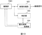
- FIG. 13 is a schematic diagram of the overall configuration of a second embodiment of the imaging apparatus according to the present invention.
- the imaging apparatus according to the present embodiment is configured by appropriately using the imaging unit 1301, the image processing unit 102, the determination unit 103, and the exposure control processing unit 104.
- the configuration of the unit 1301 and the processing in the determination unit 103 and the exposure control processing unit 104 are different from those in the first embodiment.
- the imaging unit 1301 has an “R” filter having sensitivity to a red wavelength, a “G” filter having sensitivity to a green wavelength, and blue having sensitivity to an upper portion of the photoelectric conversion element.
- the “B” filter and the “IR” filter having sensitivity in the infrared or near-infrared non-visible light region are arranged in a checkered pattern to obtain a single-plate color image pickup device that obtains four types of color signals.
- G, B, and IR are assumed to have the sensitivity characteristics shown in FIG. 10, for example.
- the wavelength distribution of the light source irradiated to the subject varies depending on the type of the light source.
- the output characteristics of the R, G, B, and IR pixels when a white subject is photographed under the light source having the distribution shown in FIG. 11, the output characteristics of the R, G, B, and IR pixels. Is a product of FIG. 10 and FIG. 11, resulting in FIG.
- the imaging unit 1301 can individually adjust the exposure time for pixels having sensitivity in the visible light region and pixels having sensitivity in the invisible light region.
- the unit 103 obtains a signal level ratio between at least one of R, G, and B signals having sensitivity in the visible light region input from the imaging unit 1301 and an IR signal having sensitivity in the invisible light region.
- the exposure control processing unit 104 individually adjusts the exposure time for each of R, G, B pixels and IR pixels of the imaging unit 1301 so that the ratio of the signal levels obtained from the determination unit 103 is constant. To do.
- the signal level ratio is obtained by obtaining average values AveG and AveIR in a predetermined image area as a signal representing white of the subject using, for example, each G signal and IR signal from the imaging unit 1301.
- AveG AveIR so that the signal level ratio is constant.
- IR pixel exposure time AveG / AveIR x G exposure time
- the wavelength distribution of the light source has the characteristics as shown in FIG. 11, so that the IR pixel is maintained while maintaining the exposure time of R, G, B having sensitivity in the visible light region.
- the signal level of the IR pixel can be increased by extending the exposure time.
- the exposure time is controlled, the amount of noise superimposed by the imaging unit 101 does not change.
- R, G, B pixels with high signal levels are in a charge saturation state, if the exposure time for R, G, B is shortened, the charge saturation can be prevented, and whiteout of the image is suppressed. It becomes possible to do.
- the average value in the predetermined image area is obtained.
- a method of extracting only a predetermined signal level in the predetermined image area may be used.
- a method of recognizing a predetermined object such as a sign of a subject and extracting a pixel of the object
- the reflection coefficients of visible light and invisible light are known for each object, the object is visible with high accuracy. The distribution of light and invisible light can be extracted.
- the imaging unit 1301 includes a reset processing unit 301 and a readout processing unit 302, and visible light individually determined by the exposure control processing unit 104 based on the signal level ratio from the determination unit 103.
- the reset processing unit 301 reads out the charge reset signal, and reads out the processing unit 302.
- a charge readout signal is generated at, and each pixel is individually controlled using these signals.
- R, G, and B are individually controlled, whereas in this embodiment, R, G, and B have the same exposure time, thereby simplifying the generation of the charge reset signal and the charge readout signal.
- the circuit scale can be reduced.
- the wiring can be simplified, and the problem that the wiring layer blocks the passage of light and reduces the aperture ratio of the pixel can be suppressed.
- the sensitivity characteristics of the visible light pixel and the invisible light pixel are assumed to be at the same level as shown in FIG. 10, but in the case of using a general image sensor such as a CMOS sensor or a CCD sensor, the visible characteristic is visible.
- the sensitivity of the invisible light pixel may be low with respect to the light pixel. Even when such an image sensor is used, adjustment can be made so that the level of each sensitivity characteristic is made uniform by changing the exposure time of visible light pixels and non-visible light pixels as in this embodiment. Can do.
- pixels having a transmission center wavelength for each of R, G, and B in the visible light region are defined as R, G, and B
- each pixel may be sensitive to invisible light, For example, it may be an R + IR pixel, a G + IR pixel, or a B + IR pixel.
- a pixel having a transmission center wavelength in the infrared or near-infrared invisible light region is defined as IR
- it may be sensitive to visible light, for example, an R + G + B + IR pixel. It may be.
- the determination unit 103 may obtain a signal level ratio after separating R, G, B, and IR by matrix calculation. *
- FIG. 6 is a schematic diagram of the overall configuration of a third embodiment of the imaging apparatus according to the present invention.
- the imaging apparatus according to the present embodiment includes an imaging unit 1301, an image processing unit 102, a non-visible light projection unit 601, a visible light projection unit 602, a table unit 603, and an exposure control processing unit 104. Configured as appropriate.
- the imaging unit 1301 has an “R” filter having sensitivity to a red wavelength, a “G” filter having sensitivity to a green wavelength, and a blue wavelength to the top of the photoelectric conversion element.
- a single-chip color image sensor that obtains four types of color signals by arranging a “B” filter with sensitivity and an “IR” filter with sensitivity in the infrared or near-infrared non-visible light region. Assume that the sensitivity characteristics of each of R, G, B, and IR are as shown in FIG. The exposure time can be individually adjusted for each of the R, G, and B pixels and the IR pixel.
- the imaging apparatus includes a non-visible light projector 601 and a visible light projector 602 that irradiate non-visible light toward a subject, and irradiation of the invisible light projector 601 is turned on. , OFF or intensity of irradiation, ON / OFF of irradiation of the visible light projecting unit 602, or intensity of irradiation, and further, each condition of the light source A irradiated at the place where the imaging apparatus of the present embodiment is installed Since the wavelength distribution of the light that finally irradiates the subject changes every time, the R, G, B pixel and IR pixel exposure times that are optimal for each condition are stored separately in advance.
- the table portion 603 is provided.
- the exposure control processing unit 104 determines whether the irradiation ON / OFF information of the invisible light projector 601 or the intensity of irradiation and the ON / OFF information of the irradiation of the visible light projector 602 or the intensity of irradiation. Based on the information, the exposure time of each of the R, G, B pixels and IR pixels is determined with reference to the information in the table unit 603, and the exposure time is adjusted individually.
- the exposure time of the IR pixel may be longer than the exposure time of the R, G, and B pixels, and each pixel may have an appropriate signal amount.
- the information on the exposure time is stored in the table unit 603 in advance, and irradiation ON / OFF information of the invisible light projector 601 or information on the intensity of irradiation and ON of the visible light projector 602 are turned on. Therefore, the exposure time is determined based on OFF information or irradiation intensity information.
- the structure which has any one may be sufficient.
- the invisible light projecting unit does not necessarily have sensitivity only to invisible light, and may have sensitivity in the visible light region.
- the visible light projecting unit is not necessarily sensitive to only visible light, and may be sensitive to invisible light.
- this invention is not limited to the above-mentioned Example, Various modifications are included.
- the above-described embodiments have been described in detail for easy understanding of the present invention, and are not necessarily limited to those having all the configurations described.
- a part of the configuration of a certain embodiment can be replaced with the configuration of another embodiment and applied as appropriate, and the configuration of another embodiment can be added to or combined with the configuration of another embodiment as appropriate. Is also possible. Further, it is possible to add, delete, and replace other configurations for a part of the configuration of each embodiment.
- each of the above-described configurations may be configured such that some or all of them are configured by hardware, or are implemented by executing a program by a processor.
- the control lines and information lines indicate what is considered necessary for the explanation, and not all the control lines and information lines on the product are necessarily shown. Actually, it may be considered that almost all the components are connected to each other. As described above, according to the configuration of each embodiment, it is possible to provide an imaging device that suppresses S / N degradation and realizes a color image with good visibility.
Landscapes
- Engineering & Computer Science (AREA)
- Multimedia (AREA)
- Signal Processing (AREA)
- Physics & Mathematics (AREA)
- Spectroscopy & Molecular Physics (AREA)
- General Physics & Mathematics (AREA)
- Color Television Image Signal Generators (AREA)
- Studio Devices (AREA)
- Exposure Control For Cameras (AREA)
- Transforming Light Signals Into Electric Signals (AREA)
Abstract
少なくとも2つ以上の異なる透過中心波長を有するカラーフィルタを備えた画素の各々について、独立して露光時間を制御する手段を設ける。
Description
本発明は、撮像装置に関する。
本技術分野の背景技術として、特開2008-92247公報(特許文献1)がある。該公報には、「[課題]固体撮像素子から出力されるカラー画像のホワイトバランスを良好にする。[解決手段]マトリックス状に配置された複数の光電変換素子20を備え、互いに異なる3つの透過中心波長を有するカラーフィルタ22R,22G, 22B、近赤外光領域に透過中心周波数を有する近赤外光フィルタ22IRのいずれか1つが光電変換素子20の各々の受光面に配置され、光電変換素子20のマトリックスの各列にカラーフィルタ22R,22G,22Bのうちいずれか1種と近赤外光フィルタ22IRが配置されている固体撮像素子により上記課題を解決することができる。」と記載されている。
撮像装置の主な用途として、監視カメラや車載カメラがある。共に、暗くなっても目的の被写体を鮮明に撮影したいという要求が強い。この課題に対しては、可視光領域の光だけではなく近赤外領域の活用による改善が記載されている。しかし、可視光領域の光量と非可視光領域の光量のいずれかが十分でない場合、ノイズに偏りが出るという課題があった。本発明は、上記課題を解決し、近赤外領域を活用してもS/N劣化を抑圧できる撮像装置を提供するものである。
本願において開示される発明のうち、代表的なものの概要を簡単に説明すれば、次の通りである。
(1)所定の透過中心波長を有する第一のフィルタを備えた第一の画素群と、前記第一のフィルタとは異なる透過中心波長を有する第二のフィルタを備えた第二の画素群と、が配列された撮像部と、前記撮像部の前記第一の画素群と前記第二の画素群の各々について独立して露光時間を制御する露光制御処理部と、を有することを特徴とする撮像装置である。
(1)所定の透過中心波長を有する第一のフィルタを備えた第一の画素群と、前記第一のフィルタとは異なる透過中心波長を有する第二のフィルタを備えた第二の画素群と、が配列された撮像部と、前記撮像部の前記第一の画素群と前記第二の画素群の各々について独立して露光時間を制御する露光制御処理部と、を有することを特徴とする撮像装置である。
本発明によれば、S/N劣化を抑圧できる撮像装置を提供することができる。
以下、本発明の実施形態について、図面を用いて説明する。
図1は、本発明に係る撮像装置の第一の実施例の全体構成概略図である。本実施例に係る撮像装置は、撮像部101と、画像処理部102と、判定部103と、露光制御処理部104と、を適宜用いて構成される。
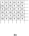
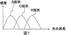
撮像部101は、例えば図2に示すように、光電変換素子の上部に赤の波長に感度を持つ“R”フィルタと、緑の波長に感度を持つ“G”フィルタ(図中ではG1とG2と記載するが、以降の本説明ではいずれの信号もGと定義して説明する)と、青に感度を持つ“B”フィルタとを市松状に配置し、これらのカラーフィルタにより各カラー信号を得る単板カラー撮像素子であるとし、R,G,B各々の画素の感度特性は、例えば図7に示すものであるとする。ここで、被写体に照射される光源の波長分布は光源の種類によって異なり、例えば図8に示す分布を有する光源下で白い被写体を写した場合、R,G,B各々の画素の出力特性は図7と図8との掛け合わせとなり、図9のようになる。この条件で撮影された白い被写体を白の映像として出力するためには、例えばBの信号レベルを小さくし、Rの信号レベルを大きくするようゲイン補正をかけ、各々の信号レベルをR=G=Bとなるように処理することで実現できる。しかし、ゲイン補正を行う前の信号にはノイズ信号が重畳しており、特に信号レベルを大きくするようゲイン補正をかけた色信号は、ノイズが強調されてしまうという課題があった。また、R,G,Bいずれかの画素が電荷飽和状態にある場合(映像が白飛びしている場合)、ゲインを下げれば飽和した画素の信号レベルは下がるが、映像の白飛びは改善されないという課題もあった。
上記課題を解決するために本実施例では、撮像部101は、R,G,Bの各画素に対して露光時間を個別に調整できるものとし、判定部103は、撮像部101から入力された各R, G,B信号の信号レベルの比を求めるものとし、露光制御処理部104は、判定部103から得た各R,G,B信号の信号レベルの比が一定になるように、撮像部101のR,G,Bの各画素の露光時間を個別に調整するものとした。
上記構成において、各R,G,B信号の信号レベルの比を求めるとは、例えば撮像部101からの各R,G,B信号に対して、被写体の白を表す信号として所定の画像領域内の平均値AveR,AveG,AveBを求め、信号レベルの比が一定になるようにとは、例えばAveR=AveG=AveBとなるように、
R画素の露光時間 = AveG / AveR × Gの露光時間
B画素の露光時間 = AveG / AveB × Gの露光時間
とすればよい。例えば撮影した画像においてAveB>AveG>AveRという条件が成り立つ場合、光源の波長分布は図8のような特性を持つため、白い被写体を白の映像として出力するために、B画素の露光時間を短くしてB画素の信号レベルを小さくすることができ、R画素の露光時間を長くしてR画素の信号レベルを大きくすることができる。また、露光時間を制御するものであるため、撮像部101で重畳されるノイズ量は変わることがない。また、信号レベルが大きかったB画素が電荷飽和状態であった場合、露光時間を短くするため電荷飽和しない状態にすることができ、映像の白飛びを抑制することが可能となる。尚、本実施例においては、被写体の白を表す信号として所定の画像領域内の平均値を求めるとしたが、所定の画像領域内のさらに所定の信号レベルのみを抽出する方法であってもよい。また、被写体の白と思われる標識などのオブジェクトを認識し、該オブジェクトの画素を抽出する方法をとれば、高精度に被写体の白を抽出することが可能となる。
R画素の露光時間 = AveG / AveR × Gの露光時間
B画素の露光時間 = AveG / AveB × Gの露光時間
とすればよい。例えば撮影した画像においてAveB>AveG>AveRという条件が成り立つ場合、光源の波長分布は図8のような特性を持つため、白い被写体を白の映像として出力するために、B画素の露光時間を短くしてB画素の信号レベルを小さくすることができ、R画素の露光時間を長くしてR画素の信号レベルを大きくすることができる。また、露光時間を制御するものであるため、撮像部101で重畳されるノイズ量は変わることがない。また、信号レベルが大きかったB画素が電荷飽和状態であった場合、露光時間を短くするため電荷飽和しない状態にすることができ、映像の白飛びを抑制することが可能となる。尚、本実施例においては、被写体の白を表す信号として所定の画像領域内の平均値を求めるとしたが、所定の画像領域内のさらに所定の信号レベルのみを抽出する方法であってもよい。また、被写体の白と思われる標識などのオブジェクトを認識し、該オブジェクトの画素を抽出する方法をとれば、高精度に被写体の白を抽出することが可能となる。
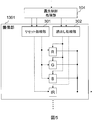
次に、上記実施例における、R,G,Bの各画素に対して個別に露光時間を独立して調整するための具体的な構成の一例を、図3を用いて説明する。撮像部101は、リセット処理部301と読み出し処理部302を有し、判定部103からのR,G,Bの各画素の信号レベルの比に基づいて露光制御処理部104にて決定されたR,G,B各画素の露光時間の情報を基に、リセット処理部301にて電荷リセット信号を、読み出し処理部302にて電荷読み出し信号を生成し、これらの信号を用いてR,G,B各画素を個別に制御する。このように、R,G,B各画素に対し、それぞれに対応する電荷リセット信号及び電荷読み出し信号を送信して制御することで、露光時間を個別に調整することが可能となる。ここで、図中には記載していないが、グローバルシャッタ方式を実現する場合、例えば、撮像部101上に配列されたすべてのR画素に対し、同一の電荷リセット信号と同一の電荷読み出し信号を送ればよい。また、ローリングシャッタ方式を実現する場合、例えば撮像部101上に配列されたすべてのR画素に対し、所定時間ずつずらした電荷リセット信号と電荷読み出し信号を送ればよい。G画素、B画素についても、R画素と同様である。この方式を採用すれば、電荷リセット信号と電荷読み出し信号生成を簡素なものとすることができ、回路規模が削減できる。また配線も簡素とすることができ、配線層が光の通り道を遮ってしまい画素の開口率を下げてしまうという問題を抑制することもできる。
尚、可視光領域のR,G,Bのそれぞれについて透過中心波長を持つ画素をR,G,Bと定義したが、各々の画素は非可視光にも感度を持つものであってもよく、例えばR+IR画素、G+IR画素、B+IR画素であってもよい。このような撮像素子を撮像部101に用いた場合、判定部103はマトリクス演算によりR,G,Bを分離したあとに信号レベルの比を求めるものとすればよい。
図13は、本発明に係る撮像装置の第二の実施例の全体構成概略図である。本実施例に係る撮像装置は、第一の実施例と同様、撮像部1301と、画像処理部102と、判定部103と、露光制御処理部104と、を適宜用いて構成されるが、撮像部1301の構成や判定部103、露光制御処理部104での処理などが第一の実施例の場合と異なる。
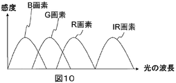
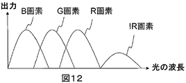
撮像部1301は、例えば図4に示すように、光電変換素子の上部に赤の波長に感度を持つ“R”フィルタと、緑の波長に感度を持つ“G”フィルタと、青に感度を持つ“B”フィルタと、赤外または近赤外の非可視光領域に感度を持つ“IR”フィルタとを市松状に配置し、4種類のカラー信号を得る単板カラー撮像素子であるとし、R,G,B,IR各々の画素の感度特性は、例えば図10に示すものであるとする。ここで、被写体に照射される光源の波長分布は光源の種類によって異なり、例えば図11に示す分布を有する光源下で白い被写体を写した場合、R,G,B,IR各々の画素の出力特性は図10と図11との掛け合わせとなり、図12のようになる。この条件で撮影された可視光領域の画像と非可視光領域の信号レベルを各々十分に確保するためには、例えば可視光領域に感度を持つR,G,B画素の信号レベルを小さくし、非可視光領域に感度を持つIR画素の信号レベルを大きくするようゲイン補正をかけ、各々の信号レベルをR=G=B=IRとなるように処理することで実現できる。しかし、ゲイン補正を行う前の信号にはノイズ信号が重畳しており、特に信号レベルを大きくするようゲインをかけたIR画素のノイズが強調されてしまうという課題があった。また、R,G,Bいずれかの画素が電荷飽和状態にある場合(映像が白飛びしている場合)、ゲインを下げれば飽和した画素の信号レベルは下がるが、映像の白飛びは改善されないという課題もあった。
上記課題を解決するために本実施例では、撮像部1301は、可視光領域に感度を持つ画素と非可視光領域に感度を持つ画素とで個別に露光時間を個別に調整できるものとし、判定部103は、撮像部1301から入力された可視光領域に感度を持つR,G,B信号の少なくともいずれかひとつと非可視光領域に感度を持つIR信号との信号レベルの比を求めるものとし、露光制御処理部104は、判定部103から得た信号レベルの比が一定になるように、撮像部1301のR,G,Bの画素とIRの画素の各々について、露光時間を個別に調整するものとした。
上記構成において、信号レベルの比を求めるとは、例えば撮像部1301からの各G信号とIR信号を用いて、被写体の白を表す信号として所定の画像領域内の平均値AveG,AveIRを求め、信号レベルの比が一定になるようにとは、例えばAveG=AveIRとなるように、
IR画素の露光時間 = AveG / AveIR × Gの露光時間
Rの露光時間 = Gの露光時間 = Bの露光時間
となるように調整すればよい。例えば撮影した画像においてAveG>AveIRという条件が成り立つ場合、光源の波長分布は図11のような特性を持つため、可視光領域に感度を持つR,G,Bの露光時間を保ちつつ、IR画素の露光時間を長くしてIR画素の信号レベルを大きくすることができる。また、露光時間を制御するものであるため、撮像部101で重畳されるノイズ量は変わることがない。また、信号レベルが大きかったR,G,B画素が電荷飽和状態であった場合、R,G,Bの露光時間を短くすれば電荷飽和しない状態にすることができ、映像の白飛びを抑制することが可能となる。尚、本実施例においては、所定の画像領域内の平均値を求めるとしたが、所定の画像領域内のさらに所定の信号レベルのみを抽出する方法であってもよい。また、被写体の標識などの所定のオブジェクトを認識し、該オブジェクトの画素を抽出する方法をとれば、物体ごとに可視光と非可視光の反射係数が各々既知である場合に、高精度に可視光と非可視光の分布を抽出することが可能となる。
IR画素の露光時間 = AveG / AveIR × Gの露光時間
Rの露光時間 = Gの露光時間 = Bの露光時間
となるように調整すればよい。例えば撮影した画像においてAveG>AveIRという条件が成り立つ場合、光源の波長分布は図11のような特性を持つため、可視光領域に感度を持つR,G,Bの露光時間を保ちつつ、IR画素の露光時間を長くしてIR画素の信号レベルを大きくすることができる。また、露光時間を制御するものであるため、撮像部101で重畳されるノイズ量は変わることがない。また、信号レベルが大きかったR,G,B画素が電荷飽和状態であった場合、R,G,Bの露光時間を短くすれば電荷飽和しない状態にすることができ、映像の白飛びを抑制することが可能となる。尚、本実施例においては、所定の画像領域内の平均値を求めるとしたが、所定の画像領域内のさらに所定の信号レベルのみを抽出する方法であってもよい。また、被写体の標識などの所定のオブジェクトを認識し、該オブジェクトの画素を抽出する方法をとれば、物体ごとに可視光と非可視光の反射係数が各々既知である場合に、高精度に可視光と非可視光の分布を抽出することが可能となる。
次に、上記実施例における、可視光領域に感度を持つ画素と非可視光領域に感度を持つ画素とで個別に露光時間を独立して調整するための具体的な構成の一例を、図5を用いて説明する。撮像部1301は、第一の実施例と同様、リセット処理部301と読み出し処理部302を有し、判定部103からの信号レベルの比から露光制御処理部104にて個別に決定された可視光領域に感度をもつR,G,B各画素の露光時間と非可視光領域に感度をもつIR画素の露光時間の情報を基に、リセット処理部301にて電荷リセット信号を、読み出し処理部302にて電荷読み出し信号を生成し、これらの信号を用いて各画素を個別に制御する。第一の実施例ではR,G,B個別に制御していたのに対し、本実施例ではR,G,Bは同一の露光時間とすることで、電荷リセット信号と電荷読み出し信号生成を簡素なものとすることができ、回路規模が削減できる。また配線も簡素とすることができ、配線層が光の通り道を遮ってしまい画素の開口率を下げてしまうという問題を抑制することができる。
また、可視光画素と非可視光画素の感度特性は、図10に示すように各々同じレベルであるとしたが、CMOSセンサやCCDセンサなどの一般的な撮像素子を用いた場合においては、可視光画素に対して非可視光画素の感度が低い場合がある。このような撮像素子を用いた場合であっても、本実施例のように、可視光画素と非可視光画素の露光時間を変えることで、各々の感度特性のレベルを揃えるように調整することができる。
尚、可視光領域のR,G,Bのそれぞれについて透過中心波長を持つ画素をR,G,Bと定義したが、各々の画素は非可視光にも感度を持つものであってもよく、例えばR+IR画素、G+IR画素、B+IR画素であってもよい。また、赤外または近赤外の非可視光領域に透過中心波長を持つ画素をIRと定義したが、可視光にも感度を持つものであってもよく、例えばR+G+B+IR画素であってもよい。このような撮像素子を撮像部1301に用いた場合、判定部103はマトリクス演算によりR,G,B,IRを分離したあとに信号レベルの比を求めるものとすればよい。
図6は、本発明に係る撮像装置の第三の実施例の全体構成概略図である。本実施例に係る撮像装置は、撮像部1301と、画像処理部102と、非可視光投光部601と、可視光投光部602と、テーブル部603と、露光制御処理部104と、を適宜用いて構成される。
撮像部1301は例えば、第二の実施例と同様、光電変換素子の上部に赤の波長に感度を持つ“R”フィルタと、緑の波長に感度を持つ“G”フィルタと、青の波長に感度を持つ “B”フィルタと、赤外または近赤外の非可視光領域に感度を持つ“IR”フィルタとを市松状に配置し、4種類のカラー信号を得る単板カラー撮像素子であり、R,G,B,IR各々の画素の感度特性は、例えば図10に示すものであるとする。また、R,G,Bの画素とIRの画素の各々について、露光時間を個別に調整できるものとした。
また、本実施例に係る撮像装置は、非可視光を被写体に向けて照射する非可視光投光部601と可視光投光部602とを備え、非可視光投光部601の照射のON,OFFまたは照射の強さ、可視光投光部602の照射のON,OFFまたは照射の強さ、さらには本実施例の撮像装置が設置される場所で照射される光源A、の各々の条件ごとに最終的に被写体に照射される光の波長分布は変わることから、事前に各々の条件に対して最適となるR,G,Bの画素とIRの画素の露光時間を個別に保存しておくテーブル部603を備える構成とした。
また、露光制御処理部104は、非可視光投光部601の照射のON,OFF情報または照射の強さの情報と可視光投光部602の照射のON,OFF情報または照射の強さの情報とを基に、テーブル部603の情報を参照してR,G,Bの画素とIRの画素の各々の露光時間を決定し、露光時間を個別に調整するものとした。
例えば、非可視光投光部601の照射をONとし、可視光投光部602の照射をONとしたとき、各々の光の波長分布の特性が図11のようになった場合、R,G,B,IR各々の画素の出力特性は図10と図11との掛け合わせとなり、図12のようになる。この場合、IR画素の露光時間は、R,G,B画素の露光時間よりも長くし、各々の画素が適正な信号量となればよい。したがって、この露光時間の情報をあらかじめテーブル部603に保持しておき、非可視光投光部601の照射のON,OFF情報または照射の強さの情報と可視光投光部602の照射のON,OFF情報または照射の強さの情報とを基に、露光時間を決定する構成とした。
以上の構成によれば、実施例1または2に記載したように画像信号から信号レベルの比を演算で求める必要がなく、処理を簡略化できる。また、映像に写っている被写体に関係なく高精度に露光時間を決定することができる。それ以外の構成、効果については、第一の実施例あるいは第二の実施例に記載のものと同様である。
尚、本実施例では非可視光投光部と可視光投光部を各々持つ構成としたが、いずれかひとつを持つ構成であってもよい。また、非可視光投光部は必ずしも非可視光のみに感度を持つものである必要はなく、可視光領域に感度を持つものであってもよい。可視光投光部は必ずしも可視光のみに感度を持つものである必要はなく、非可視光に感度を持つものであってもよい。
なお、本発明は上記した実施例に限定されるものではなく、様々な変形例が含まれる。例えば、上記した実施例は本発明を分かりやすく説明するために詳細に説明したものであり、必ずしも説明した全ての構成を備えるものに限定されるものではない。また、ある実施例の構成の一部を他の実施例の構成に置き換えて適宜適用することが可能であり、また、ある実施例の構成に他の実施例の構成を適宜追加したり組み合わせることも可能である。また、各実施例の構成の一部について、他の構成の追加・削除・置換をすることが可能である。
また、上記の各構成は、それらの一部又は全部が、ハードウェアで構成されても、プロセッサでプログラムが実行されることにより実現されるように構成されてもよい。また、制御線や情報線は説明上必要と考えられるものを示しており、製品上必ずしも全ての制御線や情報線を示しているとは限らない。実際には殆ど全ての構成が相互に接続されていると考えてもよい。
以上のように、各実施例の構成によれば、S/N劣化を抑え、視認性の良いカラー映像を実現する撮像装置を提供することができる。
以上のように、各実施例の構成によれば、S/N劣化を抑え、視認性の良いカラー映像を実現する撮像装置を提供することができる。
101・・・撮像部
102・・・画像処理部
103・・・判定部
104・・・露光制御処理部
301・・・リセット処理部
302・・・読み出し処理部
601・・・非可視光投光部
602・・・可視光投光部
603・・・テーブル部
102・・・画像処理部
103・・・判定部
104・・・露光制御処理部
301・・・リセット処理部
302・・・読み出し処理部
601・・・非可視光投光部
602・・・可視光投光部
603・・・テーブル部
Claims (7)
- 所定の透過中心波長を有する第一のフィルタを備えた第一の画素群と、前記第一のフィルタとは異なる透過中心波長を有する第二のフィルタを備えた第二の画素群と、が配列された撮像部と、
前記撮像部の前記第一の画素群と前記第二の画素群の各々について独立して露光時間を制御する露光制御処理部と、
を有することを特徴とする撮像装置。 - 請求項1に記載の撮像装置であって、
前記撮像部は、前記第一の画素群として可視光の波長領域に感度をもつ可視光画素を、前記第二の画素群として赤外または近赤外光の波長領域に感度をもつ非可視光画素とを有し、
前記露光制御処理部は、前記可視光画素と前記非可視光画素の露光時間を個別に独立して制御することを特徴とする撮像装置。 - 請求項1又は2に記載の撮像装置であって、
前記撮像部は、画素ごとの露光による蓄積電荷を放電するリセット処理部と、画素ごとの露光による蓄積電荷を読み出すための読出し処理部と、を有し、
前記露光制御処理部は、決定された露光時間に応じて前記リセット処理部と前記読み出し処理部のタイミングを制御することで、前記第一の画素群と前記第二の画素群の露光時間を制御することを特徴とする撮像装置。 - 請求項3記載の撮像装置であって、
さらに、前記撮像部から出力される前記第一の画素群からの信号と前記第二の画素群からの信号の信号レベルを比較して判定する判定部を備え、
前記露光制御処理部は、前記判定部による判定結果に基づいて、前記第一の画素群からの信号と前記第二の画素群からの信号の信号レベルが近づくように、前記撮像部の前記第一の画素群と前記第二の画素群の各々について露光時間を制御することを特徴とする撮像装置。 - 請求項4に記載の撮像装置であって、
前記判定部は、所定の画像領域内に存在する前記第一の画素群の信号レベルの平均値と前記第二の画素群の信号レベルの平均値の比を算出し、
前記露光制御処理部は、前記判定部の判定結果に基づいて、前記第一の画素群の平均値と前記第二の画素群の平均値の比が所定の比率に近づくよう、前記撮像部の前記第一の画素群と前記第二の画素群の各々について露光時間を制御することを特徴とする撮像装置。 - 請求項1又は2に記載の撮像装置であって、
さらに、少なくとも非可視光に感度を持つ光を投光する非可視光投光部を有し、
前記露光制御処理部は、前記非可視光部からの投光情報に基づいて、前記撮像部の前記第一の画素群と前記第二の画素群の各々について露光時間を制御することを特徴とする撮像装置。 - 請求項6記載の撮像装置であって、
さらに、前記投光情報に応じた露光時間情報を保持したテーブル部を備えることを特徴とする撮像装置。
Applications Claiming Priority (2)
| Application Number | Priority Date | Filing Date | Title |
|---|---|---|---|
| JP2013-019069 | 2013-02-04 | ||
| JP2013019069A JP6348254B2 (ja) | 2013-02-04 | 2013-02-04 | 撮像装置 |
Publications (1)
| Publication Number | Publication Date |
|---|---|
| WO2014119159A1 true WO2014119159A1 (ja) | 2014-08-07 |
Family
ID=51261885
Family Applications (1)
| Application Number | Title | Priority Date | Filing Date |
|---|---|---|---|
| PCT/JP2013/083814 Ceased WO2014119159A1 (ja) | 2013-02-04 | 2013-12-18 | 撮像装置 |
Country Status (2)
| Country | Link |
|---|---|
| JP (1) | JP6348254B2 (ja) |
| WO (1) | WO2014119159A1 (ja) |
Cited By (3)
| Publication number | Priority date | Publication date | Assignee | Title |
|---|---|---|---|---|
| CN113194235A (zh) * | 2021-04-29 | 2021-07-30 | 维沃移动通信有限公司 | 像素传感器系统、摄像模组及电子设备 |
| CN115134492A (zh) * | 2022-05-31 | 2022-09-30 | 北京极豪科技有限公司 | 图像采集方法、电子设备和计算机可读介质 |
| US11750948B2 (en) | 2020-11-30 | 2023-09-05 | Stmicroelectronics (Grenoble 2) Sas | Image sensors with different charge-to-voltage conversion factors and methods thereof |
Families Citing this family (4)
| Publication number | Priority date | Publication date | Assignee | Title |
|---|---|---|---|---|
| JP7039906B2 (ja) * | 2017-09-22 | 2022-03-23 | カシオ計算機株式会社 | 撮像装置、撮像方法及びプログラム |
| JP2019083501A (ja) | 2017-10-27 | 2019-05-30 | ソニーセミコンダクタソリューションズ株式会社 | 撮像装置 |
| CN108705977B (zh) * | 2018-05-09 | 2020-07-31 | 四川骏硕科技有限公司 | 一种互联网无人驾驶汽车 |
| CN113370911B (zh) * | 2019-10-31 | 2024-03-19 | 北京百度网讯科技有限公司 | 车载传感器的位姿调整方法、装置、设备和介质 |
Citations (4)
| Publication number | Priority date | Publication date | Assignee | Title |
|---|---|---|---|---|
| JP2008005213A (ja) * | 2006-06-22 | 2008-01-10 | Fujifilm Corp | 固体撮像装置およびその駆動方法 |
| JP2009066121A (ja) * | 2007-09-12 | 2009-04-02 | Sanyo Electric Co Ltd | 撮像装置 |
| WO2009057288A1 (ja) * | 2007-11-02 | 2009-05-07 | Panasonic Corporation | 撮像装置 |
| JP2010093472A (ja) * | 2008-10-07 | 2010-04-22 | Panasonic Corp | 撮像装置および撮像装置用信号処理回路 |
-
2013
- 2013-02-04 JP JP2013019069A patent/JP6348254B2/ja active Active
- 2013-12-18 WO PCT/JP2013/083814 patent/WO2014119159A1/ja not_active Ceased
Patent Citations (4)
| Publication number | Priority date | Publication date | Assignee | Title |
|---|---|---|---|---|
| JP2008005213A (ja) * | 2006-06-22 | 2008-01-10 | Fujifilm Corp | 固体撮像装置およびその駆動方法 |
| JP2009066121A (ja) * | 2007-09-12 | 2009-04-02 | Sanyo Electric Co Ltd | 撮像装置 |
| WO2009057288A1 (ja) * | 2007-11-02 | 2009-05-07 | Panasonic Corporation | 撮像装置 |
| JP2010093472A (ja) * | 2008-10-07 | 2010-04-22 | Panasonic Corp | 撮像装置および撮像装置用信号処理回路 |
Cited By (5)
| Publication number | Priority date | Publication date | Assignee | Title |
|---|---|---|---|---|
| US11750948B2 (en) | 2020-11-30 | 2023-09-05 | Stmicroelectronics (Grenoble 2) Sas | Image sensors with different charge-to-voltage conversion factors and methods thereof |
| US12096146B2 (en) | 2020-11-30 | 2024-09-17 | Stmicroelectronics (Grenoble 2) Sas | Image sensors with different charge-to-voltage conversion factors and methods thereof |
| CN113194235A (zh) * | 2021-04-29 | 2021-07-30 | 维沃移动通信有限公司 | 像素传感器系统、摄像模组及电子设备 |
| CN115134492A (zh) * | 2022-05-31 | 2022-09-30 | 北京极豪科技有限公司 | 图像采集方法、电子设备和计算机可读介质 |
| CN115134492B (zh) * | 2022-05-31 | 2024-03-19 | 北京极光智芯科技有限公司 | 图像采集方法、电子设备和计算机可读介质 |
Also Published As
| Publication number | Publication date |
|---|---|
| JP2014150470A (ja) | 2014-08-21 |
| JP6348254B2 (ja) | 2018-06-27 |
Similar Documents
| Publication | Publication Date | Title |
|---|---|---|
| JP6348254B2 (ja) | 撮像装置 | |
| US10412314B2 (en) | Systems and methods for photometric normalization in array cameras | |
| US8842194B2 (en) | Imaging element and imaging apparatus | |
| US9917998B2 (en) | Systems and methods for measuring scene information while capturing images using array cameras | |
| US20180338096A1 (en) | Image processing appartatus | |
| JP7099446B2 (ja) | 固体撮像装置および電子機器 | |
| KR100827238B1 (ko) | 고화질 영상을 위한 영상 표시 방법 및 장치 | |
| US11200647B2 (en) | Image processing | |
| WO2010116923A1 (ja) | 画像入力装置 | |
| JP2023011824A (ja) | 撮像素子 | |
| US9813687B1 (en) | Image-capturing device, image-processing device, image-processing method, and image-processing program | |
| US11089202B2 (en) | Focus adjustment for image capture device | |
| US12289541B2 (en) | Image processor and image processing system including the same | |
| US20170085769A1 (en) | Modulating light incident on imaging sensor | |
| WO2015008383A1 (ja) | 撮像装置 | |
| JP2021110885A (ja) | 撮像装置及びその制御方法 | |
| WO2020049867A1 (ja) | 撮像装置、および撮像素子 | |
| JP6600162B2 (ja) | 撮像装置およびその制御方法 | |
| JP6504892B2 (ja) | 撮像装置 | |
| JP5533752B2 (ja) | 画像信号処理装置 | |
| JP5485680B2 (ja) | 撮像装置および撮像方法 | |
| JP2010183191A (ja) | 露光量制御装置および露光量制御方法 | |
| JP2025147592A (ja) | 光波長選択制限装置、及び映像システム | |
| JP2014143497A (ja) | 固体撮像装置 | |
| JP2009177669A (ja) | 撮像装置 |
Legal Events
| Date | Code | Title | Description |
|---|---|---|---|
| 121 | Ep: the epo has been informed by wipo that ep was designated in this application |
Ref document number: 13873876 Country of ref document: EP Kind code of ref document: A1 |
|
| NENP | Non-entry into the national phase |
Ref country code: DE |
|
| 122 | Ep: pct application non-entry in european phase |
Ref document number: 13873876 Country of ref document: EP Kind code of ref document: A1 |