WO2014102880A1 - Semiconductor device, mis transistor, and multilayer wiring substrate - Google Patents
Semiconductor device, mis transistor, and multilayer wiring substrate Download PDFInfo
- Publication number
- WO2014102880A1 WO2014102880A1 PCT/JP2012/008435 JP2012008435W WO2014102880A1 WO 2014102880 A1 WO2014102880 A1 WO 2014102880A1 JP 2012008435 W JP2012008435 W JP 2012008435W WO 2014102880 A1 WO2014102880 A1 WO 2014102880A1
- Authority
- WO
- WIPO (PCT)
- Prior art keywords
- film
- insulating film
- electrode
- present
- semiconductor
- Prior art date
Links
- 239000004065 semiconductor Substances 0.000 title claims description 80
- 239000000758 substrate Substances 0.000 title description 28
- 229910000838 Al alloy Inorganic materials 0.000 claims abstract description 18
- QCWXUUIWCKQGHC-UHFFFAOYSA-N Zirconium Chemical compound [Zr] QCWXUUIWCKQGHC-UHFFFAOYSA-N 0.000 claims abstract description 9
- 229910052726 zirconium Inorganic materials 0.000 claims abstract description 9
- 239000010410 layer Substances 0.000 claims description 65
- 229910052684 Cerium Inorganic materials 0.000 claims description 9
- FYYHWMGAXLPEAU-UHFFFAOYSA-N Magnesium Chemical compound [Mg] FYYHWMGAXLPEAU-UHFFFAOYSA-N 0.000 claims description 9
- 229910052749 magnesium Inorganic materials 0.000 claims description 9
- 239000011777 magnesium Substances 0.000 claims description 9
- 239000011229 interlayer Substances 0.000 claims description 5
- GWXLDORMOJMVQZ-UHFFFAOYSA-N cerium Chemical compound [Ce] GWXLDORMOJMVQZ-UHFFFAOYSA-N 0.000 claims 4
- 238000004519 manufacturing process Methods 0.000 abstract description 18
- 239000010407 anodic oxide Substances 0.000 abstract description 14
- 238000010292 electrical insulation Methods 0.000 abstract description 4
- 239000010408 film Substances 0.000 description 176
- 239000000463 material Substances 0.000 description 54
- 229910045601 alloy Inorganic materials 0.000 description 32
- 239000000956 alloy Substances 0.000 description 32
- 238000000034 method Methods 0.000 description 19
- LYCAIKOWRPUZTN-UHFFFAOYSA-N Ethylene glycol Chemical compound OCCO LYCAIKOWRPUZTN-UHFFFAOYSA-N 0.000 description 18
- BASFCYQUMIYNBI-UHFFFAOYSA-N platinum Substances [Pt] BASFCYQUMIYNBI-UHFFFAOYSA-N 0.000 description 18
- 239000011734 sodium Substances 0.000 description 17
- 230000003647 oxidation Effects 0.000 description 16
- 238000007254 oxidation reaction Methods 0.000 description 16
- 238000009792 diffusion process Methods 0.000 description 15
- 239000008151 electrolyte solution Substances 0.000 description 14
- 229910052751 metal Inorganic materials 0.000 description 13
- 239000002184 metal Substances 0.000 description 13
- 239000013078 crystal Substances 0.000 description 12
- XLYOFNOQVPJJNP-UHFFFAOYSA-N water Substances O XLYOFNOQVPJJNP-UHFFFAOYSA-N 0.000 description 11
- 239000000126 substance Substances 0.000 description 10
- 238000010438 heat treatment Methods 0.000 description 9
- 229910052782 aluminium Inorganic materials 0.000 description 8
- 238000002048 anodisation reaction Methods 0.000 description 8
- 239000002131 composite material Substances 0.000 description 8
- 239000007789 gas Substances 0.000 description 8
- 239000002585 base Substances 0.000 description 7
- 238000004140 cleaning Methods 0.000 description 7
- 239000010949 copper Substances 0.000 description 7
- 238000004544 sputter deposition Methods 0.000 description 7
- XAGFODPZIPBFFR-UHFFFAOYSA-N aluminium Chemical compound [Al] XAGFODPZIPBFFR-UHFFFAOYSA-N 0.000 description 6
- 230000015572 biosynthetic process Effects 0.000 description 6
- MTHSVFCYNBDYFN-UHFFFAOYSA-N diethylene glycol Chemical compound OCCOCCO MTHSVFCYNBDYFN-UHFFFAOYSA-N 0.000 description 6
- 239000011521 glass Substances 0.000 description 6
- 239000000203 mixture Substances 0.000 description 6
- 239000000243 solution Substances 0.000 description 6
- 229910016952 AlZr Inorganic materials 0.000 description 5
- XLOMVQKBTHCTTD-UHFFFAOYSA-N Zinc monoxide Chemical compound [Zn]=O XLOMVQKBTHCTTD-UHFFFAOYSA-N 0.000 description 5
- 229910021417 amorphous silicon Inorganic materials 0.000 description 5
- 238000007743 anodising Methods 0.000 description 5
- 230000008901 benefit Effects 0.000 description 5
- ZMIGMASIKSOYAM-UHFFFAOYSA-N cerium Chemical compound [Ce][Ce][Ce][Ce][Ce][Ce][Ce][Ce][Ce][Ce][Ce][Ce][Ce][Ce][Ce][Ce][Ce][Ce][Ce][Ce][Ce][Ce][Ce][Ce][Ce][Ce][Ce][Ce][Ce][Ce][Ce][Ce][Ce][Ce][Ce][Ce][Ce][Ce] ZMIGMASIKSOYAM-UHFFFAOYSA-N 0.000 description 5
- 238000000576 coating method Methods 0.000 description 5
- 229910052746 lanthanum Inorganic materials 0.000 description 5
- FZLIPJUXYLNCLC-UHFFFAOYSA-N lanthanum atom Chemical compound [La] FZLIPJUXYLNCLC-UHFFFAOYSA-N 0.000 description 5
- SLIUAWYAILUBJU-UHFFFAOYSA-N pentacene Chemical compound C1=CC=CC2=CC3=CC4=CC5=CC=CC=C5C=C4C=C3C=C21 SLIUAWYAILUBJU-UHFFFAOYSA-N 0.000 description 5
- 229910052697 platinum Inorganic materials 0.000 description 5
- VYPSYNLAJGMNEJ-UHFFFAOYSA-N silicon dioxide Inorganic materials O=[Si]=O VYPSYNLAJGMNEJ-UHFFFAOYSA-N 0.000 description 5
- 239000004696 Poly ether ether ketone Substances 0.000 description 4
- 239000003990 capacitor Substances 0.000 description 4
- 238000005516 engineering process Methods 0.000 description 4
- 238000009413 insulation Methods 0.000 description 4
- 229920002530 polyetherether ketone Polymers 0.000 description 4
- 229920005989 resin Polymers 0.000 description 4
- 239000011347 resin Substances 0.000 description 4
- FLDCSPABIQBYKP-UHFFFAOYSA-N 5-chloro-1,2-dimethylbenzimidazole Chemical compound ClC1=CC=C2N(C)C(C)=NC2=C1 FLDCSPABIQBYKP-UHFFFAOYSA-N 0.000 description 3
- 239000001741 Ammonium adipate Substances 0.000 description 3
- OKTJSMMVPCPJKN-UHFFFAOYSA-N Carbon Chemical compound [C] OKTJSMMVPCPJKN-UHFFFAOYSA-N 0.000 description 3
- XUIMIQQOPSSXEZ-UHFFFAOYSA-N Silicon Chemical compound [Si] XUIMIQQOPSSXEZ-UHFFFAOYSA-N 0.000 description 3
- 235000019293 ammonium adipate Nutrition 0.000 description 3
- 230000004888 barrier function Effects 0.000 description 3
- 239000000969 carrier Substances 0.000 description 3
- 238000005229 chemical vapour deposition Methods 0.000 description 3
- 239000011248 coating agent Substances 0.000 description 3
- 239000004020 conductor Substances 0.000 description 3
- 229910052802 copper Inorganic materials 0.000 description 3
- 238000009826 distribution Methods 0.000 description 3
- 238000005530 etching Methods 0.000 description 3
- 238000004770 highest occupied molecular orbital Methods 0.000 description 3
- 239000012535 impurity Substances 0.000 description 3
- 239000004973 liquid crystal related substance Substances 0.000 description 3
- 238000004768 lowest unoccupied molecular orbital Methods 0.000 description 3
- 239000011159 matrix material Substances 0.000 description 3
- 238000000813 microcontact printing Methods 0.000 description 3
- 239000011255 nonaqueous electrolyte Substances 0.000 description 3
- 239000002245 particle Substances 0.000 description 3
- 238000001020 plasma etching Methods 0.000 description 3
- 239000000843 powder Substances 0.000 description 3
- 238000007639 printing Methods 0.000 description 3
- 230000008569 process Effects 0.000 description 3
- VSZWPYCFIRKVQL-UHFFFAOYSA-N selanylidenegallium;selenium Chemical compound [Se].[Se]=[Ga].[Se]=[Ga] VSZWPYCFIRKVQL-UHFFFAOYSA-N 0.000 description 3
- 229910052710 silicon Inorganic materials 0.000 description 3
- 239000010703 silicon Substances 0.000 description 3
- 238000004528 spin coating Methods 0.000 description 3
- 229910018072 Al 2 O 3 Inorganic materials 0.000 description 2
- IJGRMHOSHXDMSA-UHFFFAOYSA-N Atomic nitrogen Chemical compound N#N IJGRMHOSHXDMSA-UHFFFAOYSA-N 0.000 description 2
- KRHYYFGTRYWZRS-UHFFFAOYSA-N Fluorane Chemical compound F KRHYYFGTRYWZRS-UHFFFAOYSA-N 0.000 description 2
- UFHFLCQGNIYNRP-UHFFFAOYSA-N Hydrogen Chemical compound [H][H] UFHFLCQGNIYNRP-UHFFFAOYSA-N 0.000 description 2
- DGAQECJNVWCQMB-PUAWFVPOSA-M Ilexoside XXIX Chemical compound C[C@@H]1CC[C@@]2(CC[C@@]3(C(=CC[C@H]4[C@]3(CC[C@@H]5[C@@]4(CC[C@@H](C5(C)C)OS(=O)(=O)[O-])C)C)[C@@H]2[C@]1(C)O)C)C(=O)O[C@H]6[C@@H]([C@H]([C@@H]([C@H](O6)CO)O)O)O.[Na+] DGAQECJNVWCQMB-PUAWFVPOSA-M 0.000 description 2
- CBENFWSGALASAD-UHFFFAOYSA-N Ozone Chemical compound [O-][O+]=O CBENFWSGALASAD-UHFFFAOYSA-N 0.000 description 2
- 229920001665 Poly-4-vinylphenol Polymers 0.000 description 2
- 239000004734 Polyphenylene sulfide Substances 0.000 description 2
- 229910052581 Si3N4 Inorganic materials 0.000 description 2
- 229910004298 SiO 2 Inorganic materials 0.000 description 2
- 229910006404 SnO 2 Inorganic materials 0.000 description 2
- ATJFFYVFTNAWJD-UHFFFAOYSA-N Tin Chemical compound [Sn] ATJFFYVFTNAWJD-UHFFFAOYSA-N 0.000 description 2
- HSFWRNGVRCDJHI-UHFFFAOYSA-N alpha-acetylene Natural products C#C HSFWRNGVRCDJHI-UHFFFAOYSA-N 0.000 description 2
- MWPLVEDNUUSJAV-UHFFFAOYSA-N anthracene Chemical compound C1=CC=CC2=CC3=CC=CC=C3C=C21 MWPLVEDNUUSJAV-UHFFFAOYSA-N 0.000 description 2
- 239000007864 aqueous solution Substances 0.000 description 2
- NGPGDYLVALNKEG-UHFFFAOYSA-N azanium;azane;2,3,4-trihydroxy-4-oxobutanoate Chemical compound [NH4+].[NH4+].[O-]C(=O)C(O)C(O)C([O-])=O NGPGDYLVALNKEG-UHFFFAOYSA-N 0.000 description 2
- 239000002800 charge carrier Substances 0.000 description 2
- 150000001875 compounds Chemical class 0.000 description 2
- 238000013461 design Methods 0.000 description 2
- 239000003792 electrolyte Substances 0.000 description 2
- 238000011156 evaluation Methods 0.000 description 2
- 239000005357 flat glass Substances 0.000 description 2
- 229910052739 hydrogen Inorganic materials 0.000 description 2
- 239000001257 hydrogen Substances 0.000 description 2
- 230000006872 improvement Effects 0.000 description 2
- 229910052738 indium Inorganic materials 0.000 description 2
- 238000007641 inkjet printing Methods 0.000 description 2
- 230000010354 integration Effects 0.000 description 2
- 238000001755 magnetron sputter deposition Methods 0.000 description 2
- 238000005259 measurement Methods 0.000 description 2
- 150000002739 metals Chemical class 0.000 description 2
- 238000012986 modification Methods 0.000 description 2
- 230000004048 modification Effects 0.000 description 2
- 229910052750 molybdenum Inorganic materials 0.000 description 2
- 150000004767 nitrides Chemical class 0.000 description 2
- 238000000059 patterning Methods 0.000 description 2
- 238000000206 photolithography Methods 0.000 description 2
- 239000004033 plastic Substances 0.000 description 2
- 229920003023 plastic Polymers 0.000 description 2
- 229920000301 poly(3-hexylthiophene-2,5-diyl) polymer Polymers 0.000 description 2
- 229920002492 poly(sulfone) Polymers 0.000 description 2
- 229920001197 polyacetylene Polymers 0.000 description 2
- 229920001230 polyarylate Polymers 0.000 description 2
- 229910021420 polycrystalline silicon Inorganic materials 0.000 description 2
- 229920001721 polyimide Polymers 0.000 description 2
- 229920000069 polyphenylene sulfide Polymers 0.000 description 2
- 238000002360 preparation method Methods 0.000 description 2
- 230000002265 prevention Effects 0.000 description 2
- 230000009467 reduction Effects 0.000 description 2
- HQVNEWCFYHHQES-UHFFFAOYSA-N silicon nitride Chemical compound N12[Si]34N5[Si]62N3[Si]51N64 HQVNEWCFYHHQES-UHFFFAOYSA-N 0.000 description 2
- NDVLTYZPCACLMA-UHFFFAOYSA-N silver oxide Chemical compound [O-2].[Ag+].[Ag+] NDVLTYZPCACLMA-UHFFFAOYSA-N 0.000 description 2
- 229910052708 sodium Inorganic materials 0.000 description 2
- 229910052715 tantalum Inorganic materials 0.000 description 2
- PCCVSPMFGIFTHU-UHFFFAOYSA-N tetracyanoquinodimethane Chemical compound N#CC(C#N)=C1C=CC(=C(C#N)C#N)C=C1 PCCVSPMFGIFTHU-UHFFFAOYSA-N 0.000 description 2
- 239000010409 thin film Substances 0.000 description 2
- XOLBLPGZBRYERU-UHFFFAOYSA-N tin dioxide Chemical compound O=[Sn]=O XOLBLPGZBRYERU-UHFFFAOYSA-N 0.000 description 2
- QHGNHLZPVBIIPX-UHFFFAOYSA-N tin(II) oxide Inorganic materials [Sn]=O QHGNHLZPVBIIPX-UHFFFAOYSA-N 0.000 description 2
- 229910021642 ultra pure water Inorganic materials 0.000 description 2
- 239000012498 ultrapure water Substances 0.000 description 2
- 238000004506 ultrasonic cleaning Methods 0.000 description 2
- 239000011787 zinc oxide Substances 0.000 description 2
- QGZKDVFQNNGYKY-UHFFFAOYSA-N Ammonia Chemical compound N QGZKDVFQNNGYKY-UHFFFAOYSA-N 0.000 description 1
- JBRZTFJDHDCESZ-UHFFFAOYSA-N AsGa Chemical compound [As]#[Ga] JBRZTFJDHDCESZ-UHFFFAOYSA-N 0.000 description 1
- RYGMFSIKBFXOCR-UHFFFAOYSA-N Copper Chemical compound [Cu] RYGMFSIKBFXOCR-UHFFFAOYSA-N 0.000 description 1
- QPLDLSVMHZLSFG-UHFFFAOYSA-N Copper oxide Chemical compound [Cu]=O QPLDLSVMHZLSFG-UHFFFAOYSA-N 0.000 description 1
- 239000005751 Copper oxide Substances 0.000 description 1
- 229910005191 Ga 2 O 3 Inorganic materials 0.000 description 1
- GYHNNYVSQQEPJS-UHFFFAOYSA-N Gallium Chemical compound [Ga] GYHNNYVSQQEPJS-UHFFFAOYSA-N 0.000 description 1
- XEEYBQQBJWHFJM-UHFFFAOYSA-N Iron Chemical compound [Fe] XEEYBQQBJWHFJM-UHFFFAOYSA-N 0.000 description 1
- 208000022435 Light chain deposition disease Diseases 0.000 description 1
- 229910001182 Mo alloy Inorganic materials 0.000 description 1
- 229910052779 Neodymium Inorganic materials 0.000 description 1
- 239000004642 Polyimide Substances 0.000 description 1
- 229910007541 Zn O Inorganic materials 0.000 description 1
- 239000000654 additive Substances 0.000 description 1
- 230000032683 aging Effects 0.000 description 1
- 239000003513 alkali Substances 0.000 description 1
- 239000012298 atmosphere Substances 0.000 description 1
- 229910052791 calcium Inorganic materials 0.000 description 1
- 229910052799 carbon Inorganic materials 0.000 description 1
- 239000006229 carbon black Substances 0.000 description 1
- 239000002041 carbon nanotube Substances 0.000 description 1
- 229910021393 carbon nanotube Inorganic materials 0.000 description 1
- 239000000919 ceramic Substances 0.000 description 1
- 229910052804 chromium Inorganic materials 0.000 description 1
- 238000006482 condensation reaction Methods 0.000 description 1
- 229920001940 conductive polymer Polymers 0.000 description 1
- 229910000431 copper oxide Inorganic materials 0.000 description 1
- 238000005260 corrosion Methods 0.000 description 1
- 230000007797 corrosion Effects 0.000 description 1
- 230000001186 cumulative effect Effects 0.000 description 1
- 230000001419 dependent effect Effects 0.000 description 1
- 238000001514 detection method Methods 0.000 description 1
- 238000010586 diagram Methods 0.000 description 1
- 239000007772 electrode material Substances 0.000 description 1
- 238000005401 electroluminescence Methods 0.000 description 1
- 238000005868 electrolysis reaction Methods 0.000 description 1
- 125000005678 ethenylene group Chemical group [H]C([*:1])=C([H])[*:2] 0.000 description 1
- 238000002474 experimental method Methods 0.000 description 1
- 238000007667 floating Methods 0.000 description 1
- -1 for example Substances 0.000 description 1
- 229910052733 gallium Inorganic materials 0.000 description 1
- 229910052737 gold Inorganic materials 0.000 description 1
- 229910021389 graphene Inorganic materials 0.000 description 1
- 238000007646 gravure printing Methods 0.000 description 1
- 229920006015 heat resistant resin Polymers 0.000 description 1
- 230000003301 hydrolyzing effect Effects 0.000 description 1
- 230000001771 impaired effect Effects 0.000 description 1
- APFVFJFRJDLVQX-UHFFFAOYSA-N indium atom Chemical compound [In] APFVFJFRJDLVQX-UHFFFAOYSA-N 0.000 description 1
- 229910003437 indium oxide Inorganic materials 0.000 description 1
- PJXISJQVUVHSOJ-UHFFFAOYSA-N indium(iii) oxide Chemical compound [O-2].[O-2].[O-2].[In+3].[In+3] PJXISJQVUVHSOJ-UHFFFAOYSA-N 0.000 description 1
- 239000011810 insulating material Substances 0.000 description 1
- 229910052741 iridium Inorganic materials 0.000 description 1
- 238000007644 letterpress printing Methods 0.000 description 1
- 239000007788 liquid Substances 0.000 description 1
- 239000012528 membrane Substances 0.000 description 1
- 239000002923 metal particle Substances 0.000 description 1
- 238000004776 molecular orbital Methods 0.000 description 1
- 229910052759 nickel Inorganic materials 0.000 description 1
- 229910052758 niobium Inorganic materials 0.000 description 1
- 229910052757 nitrogen Inorganic materials 0.000 description 1
- 239000012299 nitrogen atmosphere Substances 0.000 description 1
- 125000004433 nitrogen atom Chemical group N* 0.000 description 1
- QJGQUHMNIGDVPM-UHFFFAOYSA-N nitrogen group Chemical group [N] QJGQUHMNIGDVPM-UHFFFAOYSA-N 0.000 description 1
- 238000007645 offset printing Methods 0.000 description 1
- 239000011368 organic material Substances 0.000 description 1
- TWNQGVIAIRXVLR-UHFFFAOYSA-N oxo(oxoalumanyloxy)alumane Chemical compound O=[Al]O[Al]=O TWNQGVIAIRXVLR-UHFFFAOYSA-N 0.000 description 1
- 229910052763 palladium Inorganic materials 0.000 description 1
- 229920002312 polyamide-imide Polymers 0.000 description 1
- 229920000767 polyaniline Polymers 0.000 description 1
- 125000005575 polycyclic aromatic hydrocarbon group Chemical group 0.000 description 1
- 239000009719 polyimide resin Substances 0.000 description 1
- 229920000642 polymer Polymers 0.000 description 1
- 229920000128 polypyrrole Polymers 0.000 description 1
- 229920000123 polythiophene Polymers 0.000 description 1
- 238000012545 processing Methods 0.000 description 1
- 239000010453 quartz Substances 0.000 description 1
- YYMBJDOZVAITBP-UHFFFAOYSA-N rubrene Chemical compound C1=CC=CC=C1C(C1=C(C=2C=CC=CC=2)C2=CC=CC=C2C(C=2C=CC=CC=2)=C11)=C(C=CC=C2)C2=C1C1=CC=CC=C1 YYMBJDOZVAITBP-UHFFFAOYSA-N 0.000 description 1
- 229910052707 ruthenium Inorganic materials 0.000 description 1
- 238000007650 screen-printing Methods 0.000 description 1
- SBEQWOXEGHQIMW-UHFFFAOYSA-N silicon Chemical compound [Si].[Si] SBEQWOXEGHQIMW-UHFFFAOYSA-N 0.000 description 1
- LIVNPJMFVYWSIS-UHFFFAOYSA-N silicon monoxide Chemical compound [Si-]#[O+] LIVNPJMFVYWSIS-UHFFFAOYSA-N 0.000 description 1
- 229910052814 silicon oxide Inorganic materials 0.000 description 1
- 229910052709 silver Inorganic materials 0.000 description 1
- 229910001923 silver oxide Inorganic materials 0.000 description 1
- 239000002356 single layer Substances 0.000 description 1
- 150000003384 small molecules Chemical class 0.000 description 1
- 229910001220 stainless steel Inorganic materials 0.000 description 1
- 239000010935 stainless steel Substances 0.000 description 1
- 230000001629 suppression Effects 0.000 description 1
- 229920001169 thermoplastic Polymers 0.000 description 1
- 229920001187 thermosetting polymer Polymers 0.000 description 1
- 239000004416 thermosoftening plastic Substances 0.000 description 1
- 229910052719 titanium Inorganic materials 0.000 description 1
- 238000012546 transfer Methods 0.000 description 1
- 238000002834 transmittance Methods 0.000 description 1
- 229910052721 tungsten Inorganic materials 0.000 description 1
- 238000001771 vacuum deposition Methods 0.000 description 1
Images

Classifications
-
- H—ELECTRICITY
- H01—ELECTRIC ELEMENTS
- H01L—SEMICONDUCTOR DEVICES NOT COVERED BY CLASS H10
- H01L29/00—Semiconductor devices adapted for rectifying, amplifying, oscillating or switching, or capacitors or resistors with at least one potential-jump barrier or surface barrier, e.g. PN junction depletion layer or carrier concentration layer; Details of semiconductor bodies or of electrodes thereof ; Multistep manufacturing processes therefor
- H01L29/66—Types of semiconductor device ; Multistep manufacturing processes therefor
- H01L29/68—Types of semiconductor device ; Multistep manufacturing processes therefor controllable by only the electric current supplied, or only the electric potential applied, to an electrode which does not carry the current to be rectified, amplified or switched
- H01L29/76—Unipolar devices, e.g. field effect transistors
- H01L29/772—Field effect transistors
- H01L29/78—Field effect transistors with field effect produced by an insulated gate
- H01L29/786—Thin film transistors, i.e. transistors with a channel being at least partly a thin film
- H01L29/78696—Thin film transistors, i.e. transistors with a channel being at least partly a thin film characterised by the structure of the channel, e.g. multichannel, transverse or longitudinal shape, length or width, doping structure, or the overlap or alignment between the channel and the gate, the source or the drain, or the contacting structure of the channel
-
- H—ELECTRICITY
- H01—ELECTRIC ELEMENTS
- H01L—SEMICONDUCTOR DEVICES NOT COVERED BY CLASS H10
- H01L21/00—Processes or apparatus adapted for the manufacture or treatment of semiconductor or solid state devices or of parts thereof
- H01L21/02—Manufacture or treatment of semiconductor devices or of parts thereof
- H01L21/02104—Forming layers
- H01L21/02107—Forming insulating materials on a substrate
- H01L21/02109—Forming insulating materials on a substrate characterised by the type of layer, e.g. type of material, porous/non-porous, pre-cursors, mixtures or laminates
- H01L21/02112—Forming insulating materials on a substrate characterised by the type of layer, e.g. type of material, porous/non-porous, pre-cursors, mixtures or laminates characterised by the material of the layer
- H01L21/02172—Forming insulating materials on a substrate characterised by the type of layer, e.g. type of material, porous/non-porous, pre-cursors, mixtures or laminates characterised by the material of the layer the material containing at least one metal element, e.g. metal oxides, metal nitrides, metal oxynitrides or metal carbides
- H01L21/02175—Forming insulating materials on a substrate characterised by the type of layer, e.g. type of material, porous/non-porous, pre-cursors, mixtures or laminates characterised by the material of the layer the material containing at least one metal element, e.g. metal oxides, metal nitrides, metal oxynitrides or metal carbides characterised by the metal
- H01L21/02178—Forming insulating materials on a substrate characterised by the type of layer, e.g. type of material, porous/non-porous, pre-cursors, mixtures or laminates characterised by the material of the layer the material containing at least one metal element, e.g. metal oxides, metal nitrides, metal oxynitrides or metal carbides characterised by the metal the material containing aluminium, e.g. Al2O3
-
- H—ELECTRICITY
- H01—ELECTRIC ELEMENTS
- H01L—SEMICONDUCTOR DEVICES NOT COVERED BY CLASS H10
- H01L21/00—Processes or apparatus adapted for the manufacture or treatment of semiconductor or solid state devices or of parts thereof
- H01L21/02—Manufacture or treatment of semiconductor devices or of parts thereof
- H01L21/02104—Forming layers
- H01L21/02107—Forming insulating materials on a substrate
- H01L21/02109—Forming insulating materials on a substrate characterised by the type of layer, e.g. type of material, porous/non-porous, pre-cursors, mixtures or laminates
- H01L21/02112—Forming insulating materials on a substrate characterised by the type of layer, e.g. type of material, porous/non-porous, pre-cursors, mixtures or laminates characterised by the material of the layer
- H01L21/02172—Forming insulating materials on a substrate characterised by the type of layer, e.g. type of material, porous/non-porous, pre-cursors, mixtures or laminates characterised by the material of the layer the material containing at least one metal element, e.g. metal oxides, metal nitrides, metal oxynitrides or metal carbides
- H01L21/02175—Forming insulating materials on a substrate characterised by the type of layer, e.g. type of material, porous/non-porous, pre-cursors, mixtures or laminates characterised by the material of the layer the material containing at least one metal element, e.g. metal oxides, metal nitrides, metal oxynitrides or metal carbides characterised by the metal
- H01L21/02189—Forming insulating materials on a substrate characterised by the type of layer, e.g. type of material, porous/non-porous, pre-cursors, mixtures or laminates characterised by the material of the layer the material containing at least one metal element, e.g. metal oxides, metal nitrides, metal oxynitrides or metal carbides characterised by the metal the material containing zirconium, e.g. ZrO2
-
- H—ELECTRICITY
- H01—ELECTRIC ELEMENTS
- H01L—SEMICONDUCTOR DEVICES NOT COVERED BY CLASS H10
- H01L21/00—Processes or apparatus adapted for the manufacture or treatment of semiconductor or solid state devices or of parts thereof
- H01L21/02—Manufacture or treatment of semiconductor devices or of parts thereof
- H01L21/02104—Forming layers
- H01L21/02107—Forming insulating materials on a substrate
- H01L21/02109—Forming insulating materials on a substrate characterised by the type of layer, e.g. type of material, porous/non-porous, pre-cursors, mixtures or laminates
- H01L21/02112—Forming insulating materials on a substrate characterised by the type of layer, e.g. type of material, porous/non-porous, pre-cursors, mixtures or laminates characterised by the material of the layer
- H01L21/02172—Forming insulating materials on a substrate characterised by the type of layer, e.g. type of material, porous/non-porous, pre-cursors, mixtures or laminates characterised by the material of the layer the material containing at least one metal element, e.g. metal oxides, metal nitrides, metal oxynitrides or metal carbides
- H01L21/02175—Forming insulating materials on a substrate characterised by the type of layer, e.g. type of material, porous/non-porous, pre-cursors, mixtures or laminates characterised by the material of the layer the material containing at least one metal element, e.g. metal oxides, metal nitrides, metal oxynitrides or metal carbides characterised by the metal
- H01L21/02194—Forming insulating materials on a substrate characterised by the type of layer, e.g. type of material, porous/non-porous, pre-cursors, mixtures or laminates characterised by the material of the layer the material containing at least one metal element, e.g. metal oxides, metal nitrides, metal oxynitrides or metal carbides characterised by the metal the material containing more than one metal element
-
- H—ELECTRICITY
- H01—ELECTRIC ELEMENTS
- H01L—SEMICONDUCTOR DEVICES NOT COVERED BY CLASS H10
- H01L21/00—Processes or apparatus adapted for the manufacture or treatment of semiconductor or solid state devices or of parts thereof
- H01L21/02—Manufacture or treatment of semiconductor devices or of parts thereof
- H01L21/02104—Forming layers
- H01L21/02107—Forming insulating materials on a substrate
- H01L21/02225—Forming insulating materials on a substrate characterised by the process for the formation of the insulating layer
- H01L21/02227—Forming insulating materials on a substrate characterised by the process for the formation of the insulating layer formation by a process other than a deposition process
- H01L21/02258—Forming insulating materials on a substrate characterised by the process for the formation of the insulating layer formation by a process other than a deposition process formation by anodic treatment, e.g. anodic oxidation
-
- H—ELECTRICITY
- H01—ELECTRIC ELEMENTS
- H01L—SEMICONDUCTOR DEVICES NOT COVERED BY CLASS H10
- H01L29/00—Semiconductor devices adapted for rectifying, amplifying, oscillating or switching, or capacitors or resistors with at least one potential-jump barrier or surface barrier, e.g. PN junction depletion layer or carrier concentration layer; Details of semiconductor bodies or of electrodes thereof ; Multistep manufacturing processes therefor
- H01L29/40—Electrodes ; Multistep manufacturing processes therefor
- H01L29/43—Electrodes ; Multistep manufacturing processes therefor characterised by the materials of which they are formed
- H01L29/49—Metal-insulator-semiconductor electrodes, e.g. gates of MOSFET
- H01L29/4908—Metal-insulator-semiconductor electrodes, e.g. gates of MOSFET for thin film semiconductor, e.g. gate of TFT
-
- H—ELECTRICITY
- H01—ELECTRIC ELEMENTS
- H01L—SEMICONDUCTOR DEVICES NOT COVERED BY CLASS H10
- H01L23/00—Details of semiconductor or other solid state devices
- H01L23/52—Arrangements for conducting electric current within the device in operation from one component to another, i.e. interconnections, e.g. wires, lead frames
- H01L23/522—Arrangements for conducting electric current within the device in operation from one component to another, i.e. interconnections, e.g. wires, lead frames including external interconnections consisting of a multilayer structure of conductive and insulating layers inseparably formed on the semiconductor body
- H01L23/532—Arrangements for conducting electric current within the device in operation from one component to another, i.e. interconnections, e.g. wires, lead frames including external interconnections consisting of a multilayer structure of conductive and insulating layers inseparably formed on the semiconductor body characterised by the materials
- H01L23/5329—Insulating materials
-
- H—ELECTRICITY
- H01—ELECTRIC ELEMENTS
- H01L—SEMICONDUCTOR DEVICES NOT COVERED BY CLASS H10
- H01L2924/00—Indexing scheme for arrangements or methods for connecting or disconnecting semiconductor or solid-state bodies as covered by H01L24/00
- H01L2924/0001—Technical content checked by a classifier
- H01L2924/0002—Not covered by any one of groups H01L24/00, H01L24/00 and H01L2224/00
Definitions
- the present invention relates to a semiconductor device, a MIS transistor, and a multilayer wiring board.
- High integration and high density of semiconductor devices depend on miniaturization of electronic functional elements such as transistor switching elements. As the electronic functional element becomes finer, the electrical characteristics and operational reliability of each component constituting the element are further improved, and the electrical characteristics and operational characteristics among many electronic elements constituting the semiconductor device. There is a need for further improvement in variability.
- MISTr Metal-Insulator-semiconductor type transistor
- MIMSWE non-linear resistance element
- MISTr Metal-Insulator-semiconductor
- MIMSWE metal-insulator-Metal type switching element
- MISTr and MIMSWE insulation are also used for the electrical quality and reliability of electrical insulation films in capacitors used in many electrical circuits of semiconductor devices and multilayer wiring boards that have at least part of the MIM type wiring structure. There is a demand equal to or greater than the demand for membranes.
- the demand for simplification of the production process of electrical insulating films, simplification of production facilities, and reduction of production costs in electronic functional elements, capacitors and MIM type wiring structures is the competitiveness of finished electrical and electronic equipment. It is getting stronger year by year.
- the formation method of the insulating film by the anodic oxidation method has a possibility of becoming a powerful insulating film forming method.
- an example in which an insulating film having an MIM type wiring structure is formed is described in Patent Document 1, and an example in which a gate insulating film of MISTr is formed in Patent Document 2.
- the electrolytic solution for anodization is composed of ethylene glycol, ammonium tartrate, and water, and the concentration of ethylene glycol is high.
- the temperature of the electrolytic solution is about 25 ° C.
- the temperature is 40 ° C. or lower. Dissolved during anodization, the anodization speed is dependent on the film surface, and it is difficult to form an oxide film with excellent surface smoothness, which is an important film factor in the semiconductor field. is there. In addition, since the temperature of the electrolyte during anodization is low, mass production efficiency does not increase.
- the present invention has been devised in view of the above points, and one of its purposes is to provide a semiconductor device including a highly durable electrical insulating film that can be produced and managed with high efficiency and can save costs. is there.
- Another object is to provide a multilayer wiring board for a semiconductor device provided with a highly durable interlayer insulating film that can be efficiently managed and cost-saving.
- the insulating film is an anodized film of an aluminum alloy to which 0.01 to 0.15% of zirconium is added.
- the semiconductor device is characterized in that the aluminum alloy does not include at least one of magnesium and cerium.
- Another aspect of the present invention is an anodization of an aluminum alloy in which zirconium is added in an amount of 0.01 to 0.15% in a multilayer wiring board for a semiconductor device having an interlayer insulation film.
- the multilayer wiring board for semiconductor devices is characterized by being a film (provided that the aluminum alloy does not include at least one of magnesium and cerium).
- the gate insulating film has a zirconium content of 0.01-0. It is an MIS transistor characterized by being an anodized film of aluminum alloy added with 15% (however, the aluminum alloy does not contain at least one of magnesium and cerium).
- Still another aspect of the present invention is an aluminum alloy anode in which 0.01 to 0.15% of zirconium is added to the MIM type insulating film in a semiconductor device having an MIM type structure.
- the semiconductor device is an oxide film (provided that the aluminum alloy does not include at least one of magnesium and cerium).
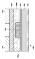
- FIG. 1 is a schematic configuration diagram for explaining the configuration of a MISTr that is one of the preferred embodiments of the present invention.
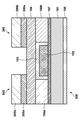
- FIG. 2 is a schematic configuration explanatory view for explaining the configuration of a MISTr which is another example of a preferred embodiment of the present invention.
- FIG. 3 is a schematic configuration explanatory view for explaining the configuration of a MISTr which is still another example of the preferred embodiment of the present invention.
- the MISTr 100 shown in FIG. 1 includes a gate electrode 102, a gate insulating film 103, a semiconductor layer 104, a source electrode 105, and a drain electrode 106 on a semiconductor substrate 101.
- planarizing layer regions 109a and 109b are provided in advance on the left and right sides of the gate insulating film 103 so that the surface thereof is aligned with the upper surface of the gate insulating film 103 in order to eliminate a step when the semiconductor layer 104 is provided.
- the base body 100 is an inexpensive glass substrate such as blue plate glass, for example, sodium (Na) contained in the glass substrate is prevented from diffusing outside the substrate.
- a diffusion prevention layer 107 is provided as necessary.
- a chemical resistant Na diffusion preventing layer 108 having a chemical resistance function, in particular an etching chemical resistance function, in addition to the Na diffusion preventing function is provided on the lower surface of the base 100, sodium ( This is advantageous because it not only prevents the diffusion of Na) but also prevents the etching of the glass substrate by chemicals used in the manufacturing process of MISTr100, such as buffered hydrofluoric acid.
- Both the Na diffusion preventing layer 107 and the chemical resistant Na diffusion preventing layer 108 may be made of the same material, or may be made of different materials depending on the characteristics required for each layer.
- the following organic composition (A) described in the international publication 2010/001793 is mentioned as a preferable material, for example.
- Organic composition (A) A composition represented by the general formula ((CH 3 ) SiO 3/2 ) x (SiO 2 ) 1-x (where 0 ⁇ x ⁇ 1.0).
- preferred examples include condensates obtained by subjecting a mixture of a methyltrialkoxysilane compound and a tetraalkoxysilane compound to a hydrolytic condensation reaction.
- the coating solution containing this condensate is applied to form a coating film, and the coating film is heat-treated at a temperature of 400 ° C. or lower to form the Na diffusion preventing layer 107 or the chemical resistant Na diffusion preventing layer 108. .
- the film thickness excellent characteristics such as a Na diffusion preventing function are maintained even if the film thickness is reduced to about 150 to 300 nm. Insulation characteristics are also excellent.
- the current density is 1 ⁇ 10 ⁇ 10 A / cm 2 at 1 MV / cm, and the current density is 1 ⁇ 10 ⁇ 9 A / cm 2 at 3 MV / cm.
- the gate insulating film 103 needs to be formed by selecting a material and a manufacturing process / condition that can ensure gate capacitance and prevention (or suppression) of leakage current.
- the gate insulating film 103 is made of an electrolytic solution having a liquid composition described later for an aluminum (Al) alloy (“Al (Zr) alloy”) film to which zirconium (Zr) is added. It is formed by anodizing.
- the Al (Zr) alloy film provided for forming the gate insulating film 103 may be the one provided for forming the gate electrode 102 or the one provided on the gate electrode 102.
- the Al (Zr) alloy film is an alloy film provided for forming the gate electrode 102, only the upper part of the Al (Zr) alloy film is anodized to form the gate insulating film 103, and the lower part is made of an Al (Zr) alloy.
- the gate electrode 102 is left as it is.
- the gate insulating film 103 is formed by anodizing a part of the upper part of the Al (Zr) alloy film provided for forming the gate electrode 102, and the remaining lower part which is not anodized is the gate electrode 102.
- the Al (Zr) alloy for forming the gate insulating film 103 by anodic oxidation is an Al alloy mainly composed of aluminum (Al) and added with zirconium (Zr). , Either magnesium or cerium is not included).
- the amount of zirconium (Zr) added to the alloy is appropriately determined according to the desired electrical characteristics in design of the gate insulating film 103 to be formed. Further, when the gate electrode 102 is composed of an Al (Zr) alloy film, the gate electrode 102 is formed at a predetermined temperature with respect to the anodic oxide film formed by anodizing the Al (Zr) alloy film to form the gate insulating film 103. Since heat treatment is performed for a predetermined time, the addition amount of Zr is set as desired in order to prevent or suppress the growth of the Al 2 O 3 crystal grains in the anodic oxide film formed by this heat treatment to an unacceptably large size. Are appropriately selected. The amount of Zr added in the present invention is preferably 0.01% to 0.15%.
- the balance excluding the above-mentioned amount of additives is preferably made of Al and inevitable impurities, and each of the inevitable impurities is preferably 0.01% or less.
- the inevitable impurities include silicon (Si), iron (Fe), copper (Cu), and the like.
- the Al (Zr) alloy film is formed using a rotating magnetron sputtering apparatus.
- the rotating magnetron sputtering apparatus are described in International Publication No. 2007/043476, International Publication No. 2008/114718, and the like.
- the temperature of the film forming substrate is preferably about room temperature to 200 ° C., and a Kr / O 2 (O 2 : 1 to 5%) mixed gas is used as the sputtering gas.
- the film thickness of the alloy film to be formed can be appropriately determined as desired depending on whether the entire film is anodized or a part of the film is anodized into a film shape.
- a part of the film is a gate electrode and the remaining part is anodized, it is preferably 1 to 3 ⁇ m.
- the anodic oxidation of the Al (Zr) alloy film is carried out as follows, but is not limited to this, as long as the production process and production conditions are within the scope of the object of the present invention. This is the category of the present invention.
- a preferable electrolytic solution used in the anodic oxidation in the present invention is a nonaqueous aqueous anodic oxidation electrolytic solution (A) described below.
- Non-aqueous electrolyte solution for anodic oxidation (A) Solution (1): ethylene glycol (79%) Ammonium adipate (1%) Water (20%)
- An Al (Zr) alloy film (sample A) prepared on a desired substrate is immersed in an anodic oxidation bath filled with a predetermined amount of these electrolytic solutions (A), and a counter electrode made of Pt (platinum) A voltage is applied between (Pt) and anodic oxidation.
- anodic oxidation is performed by supplying a current having a current density in the range of 0.1 to 0.2 mA / cm 2 at a constant level (constant current mode).
- the voltage (V) between the anodized surface of the sample (1) and the counter electrode (Pt) gradually increases.
- the voltage (V) rises to a voltage in the range of 25-50V, switch to constant voltage mode.
- the current (A) flowing between the sample (1) and the counter electrode (Pt) becomes a value sufficiently lower than 1 ⁇ A / cm 2 , the anodic oxidation is finished. Thereafter, the sample (1) is sufficiently washed with ultrapure water.
- the temperature is gradually raised to 300 ° C. in a reduced pressure (1 to 10 Torr) N 2 gas atmosphere, and this state is maintained for 1 to 10 hours, preferably 3 to 7 hours.
- a normal pressure is maintained at 300 ° C. for 1 to 3 hours while flowing 100% O 2 gas.
- the non-aqueous electrolyte solution (A) according to the present invention When the non-aqueous electrolyte solution (A) according to the present invention is used, a non-porous, dense and uniform highly insulating anodic oxide film (barrier type) is formed over a large area from an extremely thin film to a thick film. However, it can be reliably and efficiently formed. One reason for this is described below.
- the relative dielectric constant of water is as high as 80, so that water molecules dissociate into H + and OH ⁇ at a low voltage.
- anodic oxide film with a certain thickness on the Al (Zr) alloy film surface In order to form an anodic oxide film with a certain thickness on the Al (Zr) alloy film surface, a voltage of at least 200 V or more must be applied between the counter electrode and the Pt (platinum) electrode.
- the electrical resistance of the anodic oxide film is not so strong, and it is generally difficult to form a film to a certain thickness. Therefore, in the present invention, it is desirable to add ethylene glycol or diethylene glycol having a small relative dielectric constant to form a non-aqueous solution, and it is preferable to lower the relative dielectric constant to about 51 to 44.
- the barrier type anodic oxide film of Al (Zr) alloy formed in the non-aqueous electrolyte solution according to the present invention has excellent characteristics as a passive film. Further, the microroughness on the surface of the oxide film is very small as compared with the oxide film formed by the aqueous electrolyte solution. Furthermore, even at high temperatures, the barrier type anodic oxide film according to the present invention does not generate thermal cracks and the like, and the amount of moisture released as outgas from the film is very small. Shows remarkable corrosion resistance.
- the anodic oxide film according to the present invention can be obtained with a predetermined film thickness by adjusting the relative dielectric constant of the electrolytic solution and the applied voltage during anodic oxidation.
- the thickness of the anodic oxide film is appropriately determined according to the characteristics required for the insulating film constituting the electronic element to be formed and the interlayer insulating film of the multilayer wiring board.
- the thickness of the anodized film is preferably 5 to 100 nm, more preferably 10 to 70 nm, and still more preferably 30 to 60 nm.
- the anodized film derived from the Al (Zr) alloy formed by the anodic oxidation method is substantially composed of aluminum oxide (Al 2 O 3 ), including substantially the whole film, including substantially the whole film.
- Al oxide Al 2 O 3
- an oxide of a metal (Zr) derived from an Al (Zr) alloy is intentionally mixed into the anodized film in order to satisfy the characteristics required for the insulating film.
- the non-aqueous electrolytic solution used in the present invention contains the components as described above, and is adjusted to have a predetermined dielectric constant and pH. In the nonaqueous electrolytic solution that can be used in the present invention, it is not denied that other necessary chemical components are included as long as the object of the present invention is not impaired.
- various materials can be used as the substrate 101, but heat-resistant plastic, glass, metal, ceramics, etc. are preferably employed.
- examples of such materials include quartz, blue plate glass, alkali metal-less glass, silicon (silicon) substrate, metal substrate such as aluminum and stainless steel, semiconductor substrate such as gallium arsenide (GaAs), and thermoplastic or thermosetting.
- a plastic substrate or the like is used.
- stacked 2 or more types of the said material can also be used.
- the gate electrode 102 most of conductive materials for electrodes or electric wiring used in the semiconductor field can be used.
- conductive materials include Cr, Al, Ta, Mo, Nb, Cu, Ag, Au (4.9 eV), Pt, Pd, In, Ni, Nd, Ca, Ti, Ta, Ir, and Ru. , W, Mo, Ru-Mo alloys, etc. and alloys of these metals (hereinafter referred to as “metal (M)”, but “M ⁇ (Zr)”) or Al (Zr) alloys Composed.
- conductive oxides such as InO 2 , Sn 2 and ITO, conductive nitrides such as TiN and TaN, conductive polymers such as polyaniline, polypyrrole, polythiophene or polyacetylene, graphene, carbon nanotubes, charge transfer complexes Molecular conductors such as those, and their laminated structure members. Further, a conductive composite material in which carbon black or metal particles are dispersed may be used.
- the gate electrode 102 be formed as thin as possible within the range where the electrode function is exhibited and no pinhole is generated in consideration of the flatness of the layer (or film) formed thereon. Specifically, it is desirable that the film is formed with a thickness of usually 100 nm or less, preferably 50 nm or less, more preferably 10 nm or less.
- the gate electrode 102 is not limited to a single layer structure made of a single material selected from the above materials.
- a single material selected from the above materials preferably using different materials selected from conductive oxides such as InO 2 , SnO 2 , ITO, conductive nitrides such as TiN, TaN, metals (M), Al (Zr) alloys
- conductive oxides such as InO 2 , SnO 2 , ITO, conductive nitrides such as TiN, TaN, metals (M), Al (Zr) alloys
- a composite film structure may be used. If such a composite film is shown in a configuration in which layers are sequentially laminated from the base 101 side, for example, the following electrode configuration is preferable.
- the gate electrode length is appropriately determined according to the element design, but preferably 2 to 10 ⁇ m.
- the source electrode and the drain electrode may be composed of a single material film alone, or may be composed of a composite film (laminated structure film / multilayer film structure) composed of different metal (M) materials.
- a composite film laminated structure film / multilayer film structure
- M metal
- the semiconductor layer 104 in the present invention is composed of an organic semiconductor material or an inorganic semiconductor material.
- a semiconductor material may be crystalline or amorphous, but in the case of crystalline, it may be a single crystal, but it is polycrystalline or microcrystalline in that a large-area device can be easily manufactured. Is preferred.
- Organic semiconductor materials include polycyclic aromatic hydrocarbons such as pentacene, anthracene and rubrene, low molecular weight compounds such as tetracyanoquinodimethane (TCNQ), polyacetylene, poly-3-hexylthiophene (P3HT), poly Examples include polymers such as paraphenylene vinylene (PPV).
- polycyclic aromatic hydrocarbons such as pentacene, anthracene and rubrene
- TCNQ tetracyanoquinodimethane
- P3HT poly-3-hexylthiophene
- PV paraphenylene vinylene
- Amorphous silicon is amphoteric, both p-type using holes as charge carriers and n-type using electrons as charge carriers, most of which are n-type.
- copper oxide, silver oxide, and tin monoxide have been reported as p-type.
- TFTs Transparent Amorphous Oxide Semiconductors
- TFTs Thin film transistors
- TAOS-based inorganic semiconductor materials have a high carrier mobility of 10 cm 2 / Vs or more and small variations in characteristics, which is a problem for organic EL panels.
- display unevenness due to variation in characteristics of the display can be suppressed.
- the TAOS film can be formed by sputtering, the manufacturing cost can be reduced.
- the manufacturing process temperature can be lowered to near room temperature, a resin substrate with poor heat resistance can be used, flexible displays such as electronic paper that can be bent, and transparent displays that take advantage of the transparency can be easily realized. .
- amorphous In-Ga-Zn-O ((1) high mobility, (2) high off-performance, and (3) high productivity) (Hereinafter sometimes referred to as “IGZO”) is a more preferred material.
- IGZO has 20 to 50 times the electron mobility of a-Si used for TVs (TVs) and monitors, so TFTs can be miniaturized and wires can be thinned.
- IGZO-LCD is equivalent. It is possible to achieve a high-definition that can be easily doubled with a transmittance of. In addition, further reduction in power consumption can be realized by high off-performance.
- a pause period can be provided, and power consumption can be reduced. It can be reduced to 1/5 to 1/10. If this pause period is provided in the a-Si display panel, flicker occurs. However, if IGZO is used, it can be realized without flicker. Due to the high off-performance, it is possible to improve the performance of the touch panel. For example, by using pause driving, the SN ratio can be improved by a factor of 5, and the touch detection performance can be significantly improved.
- the MISTr that constitutes the semiconductor layer with IGZO having such advantages can exhibit the advantages more effectively by using the gate insulating film as the anodic oxide film of the present invention. Is a more preferred combination.
- the source electrode 105 and the drain electrode 106 are preferably made of a material that is appropriately selected in relation to the material that forms the semiconductor layer 104 so that electrical contact with the semiconductor layer 104 is smooth.
- the source electrode 105 is made of a material having a small work function.
- the semiconductor layer 104 of an organic semiconductor material such as pentacene and have n-type operating characteristics, it is as consistent as possible with LUMO (Lowest Unoccupied Molecular Orbital) of the organic semiconductor material (3.2 eV in the case of pentacene).
- the material is appropriately selected so as to take off. As a result, electrons can be easily injected from the source electrode 105 into the LUMO of the material forming the semiconductor layer 104.
- the material selection criteria for the drain electrode 106 are the same as the material selection criteria for the source electrode 105 in the sense of smooth carrier movement at the contact interface. That is, in the case of the drain electrode 106, a material that facilitates the emission of electrons from the HOMO (Highest Occupied Molecular Orbital) of the material constituting the semiconductor layer 104 to the drain electrode 106 is selected. That is, when the active layer region 104 is made of an organic semiconductor material and has p-type operating characteristics, the organic semiconductor material has a HOMO (HighestccOccupied Molecular Orbital) (5.0 eV in the case of pentacene) as much as possible. The material is appropriately selected so as to achieve consistency.
- HOMO HighestccOccupied Molecular Orbital
- the heat resistant temperature is 150 ° C. or more, for example, polyarylate (PAR), polysulfone (PSF), polyphenylene sulfide (PPS), It is preferable to employ polyether ether ketone (PEEK), polyimide resin, fluororesin or the like.
- PAR polyarylate
- PSF polysulfone
- PPS polyphenylene sulfide
- PEEK polyether ether ketone
- polyimide resin fluororesin or the like.
- PAI polyamideimide
- PEEK polyetheretherketone
- polyvinyl phenol (PVPh) capable of forming an ultrathin film without pinholes is also a particularly preferred material in the present invention.
- the planarization region 110 is made of resin, and is made of an inorganic insulating material such as silicon oxide (SiO 2 ), silicon nitride (Si 3 N 4 ), silicon oxynitride (SiNO), or silicon carbonitride (SiCN). Also good.
- the MISTr 200 shown in FIG. 2 has a gate electrode 202, a gate insulating film 203, a semiconductor layer 204, a source electrode 205, a drain electrode 206, and a planarization layer on a semiconductor substrate 201, similarly to the MISTr 100 shown in FIG. An area 209 is provided.
- the base 201 is the base 101
- the gate electrode 202 is the gate electrode 102
- the gate insulating film 203 is the gate insulating film 103
- the semiconductor layer 204 is the semiconductor layer 104
- the source electrode 205 is the source electrode.
- the drain electrode 206 corresponds to the drain electrode 106
- the planarization layer region 209 corresponds to the planarization layer region 109, respectively, and the same materials and production conditions as in the case of the MISTr 100 are applied.
- the unstrained Na diffusion preventing layer 207 and the unstrained / chemical resistant Na diffusion preventing layer 208 are provided as necessary.
- the feature of the layers 207 and 208 is that the layers themselves are not distorted. This distortion-free property hardly changes when MISTr200 is exposed to high temperatures up to about 100 ° C.
- a material constituting the layers 207 and 208 for example, SiCN in which about 10% of carbon (C) is added to silicon nitride (Si 3 N 4 ) is preferable.
- the source electrode and the drain electrode are made of a material appropriately selected in relation to the material constituting the semiconductor layer so that the electrical contact with the semiconductor layer becomes smooth. Such an example is shown in FIG.
- the MISTr 300 shown in FIG. 3 is the same as the MISTr 100 shown in FIG. 1 except that the source electrode portion 305 and the drain electrode portion 306 are different from the source electrode 105 and the drain electrode 106, respectively.
- the same reference numerals as in FIG. 1 are used.
- the lower electrode film 305a of the source electrode portion 305 is made of a material having a low work function
- the lower electrode film 306a of the drain electrode portion 306 is made of a material having a high work function. The driving ability is improved.
- the semiconductor layer 104 is formed of an intrinsic or substantially intrinsic semiconductor material such as pentacene
- carriers contributing to conduction are not present in the semiconductor layer 104 or are substantially or hardly present. It is necessary to improve current driving capability by injecting carriers. Therefore, in order to make it easier for carriers to be injected into the semiconductor layer 104 in relation to the work function of the semiconductor layer 104, the lower electrode film 305a having a relatively low work function and the lower electrode film 306a having a high work function are used.
- a stacked structure of an upper electrode region 305b made of an inexpensive and easy-to-handle material and a lower electrode region 305a made of a material having a small work function may be used.
- the upper electrode region 305b is made of a metal such as Al or Cu
- the lower electrode region 305a is made of lanthanum boride or the like.
- the lower electrode region 305a is preferably composed of LaB 6 (N) having the characteristics described later.
- the upper electrode region 306b is made of Al and the lower electrode region 306a is made of Ni.
- a film forming method in the case of forming a film with an organic material, various film forming methods are adopted depending on the characteristics and application of the electronic element to be formed and the film forming material to be used.
- the film forming method that can be employed in the present invention include a coating method, a vacuum deposition method, CVD (Chemical Vapor Deposition), PCVD (Plasma Chemical Vapor Deposition), and the like.
- the coating method include spin coating, casting, and printing.
- the printing method include offset printing, letterpress printing, intaglio printing, gravure printing, screen printing, ink jet printing, and micro contact printing.
- the definition is 10 ⁇ m or less, it is preferable to employ ink jet printing or micro contact printing.
- ink jet printing or micro contact printing it is known that the switching characteristics of an element are improved by reducing the distance between the source electrode and the drain electrode (channel length: L). It is desirable to employ microcontact printing that allows area patterning.
- the semiconductor layer (104, 204) when the semiconductor layer (104, 204) is made of a semiconductor material with low mobility and is operated n-type, the semiconductor layer (104, 204) and the gate insulating film (103, 203) or the semiconductor layer It is desirable to provide the electron supply layer region (X) near the gate insulating film (103, 203) side in the semiconductor layer (104, 204) adjacent to or close to the channel region formed in (104, 204). .
- the electron supply layer region (X) is made of a low work function material that easily emits electrons.
- a material is lanthanum boride (LaB 6 : lanthanum hexaboride).
- LaB 6 (N) lanthanum boride containing nitrogen
- the layer region (X) is more preferably composed of a LaB 6 (N) film described below.
- a more preferable LaB 6 (N) film has a crystal structure, contains 0.3 to 0.5 atomic% of nitrogen atoms, and has a crystal grain size range of 10 to 250 nm in all the crystals in the film.
- the present inventors presume that not only the LaB 6 film having a low work function of 2.4 eV but also the interface affinity with the semiconductor layer (104, 204) is set within the above numerical range. Since it is excellent, it is considered that the film has good interface characteristics and good adhesion. Therefore, the desired adhesion is maintained even when the cumulative usage time of the device becomes considerably long, and the film becomes a LaB 6 (N) film with excellent aging resistance characteristics without causing film floating or film peeling. I think that the.
- the proportion of the crystals in the particle size range of 10 to 250 nm in all the crystals in the film is preferably in the above numerical range, more preferably 50 to 90%, still more preferably 80%. It is desirable to be ⁇ 90%. Even more preferably, the proportion of crystals in the particle size range of 30 to 200 nm is desirably 50 to 90%. Further, it is particularly desirable that the proportion of crystals in the particle size range of 50 to 150 nm is 50 to 90%.
- the crystallinity of the film is also important for obtaining a better nitrogen-containing lanthanum hexaboride (“LaB 6 (N)”) film.
- the degree of crystallinity is preferably 20% or more as described above, more preferably 30% or more, and still more preferably 50% or more.
- the peak position of the crystal grain size distribution is also an important parameter for obtaining a more suitable LaB 6 (N) film of the present invention.
- the maximum of the grain size distribution peak in the range of 10 to 250 nm is desirably within 15 to 150 nm, more preferably 15 to 120 nm, and still more preferably 20 It is desirable to be in the range of ⁇ 100 nm.
- Example 1 Measurement of leakage current and measurement of film uniformity / denseness Preparation of “Sample A” The surface was cleaned according to a cleaning method commonly used in the semiconductor field, and the size was 10 (cm) ⁇ 10 (cm) A quartz glass plate was prepared. On this quartz glass plate, a MIM type electrode structure was formed using a sputtering technique, a photolithography technique, and an anodic oxidation method of an AlZr (0.1%) alloy film according to the present invention, which are usually performed in the semiconductor field.
- the lower electrode part of the electrode structure part has a configuration in which 10 stripe-shaped aluminum (Al) electrodes having a width of 5 (mm) x a length of 8 (cm) are arranged at a pitch of 2 (mm) on the quartz glass plate. It was.
- a laminate in which an anodic oxide film having a width of 5 mm and a length of 5 mm and an aluminum (Al) individual electrode having the same size as that of the anodic oxide film is provided thereon is 10 They are arranged in a ⁇ 10 matrix (100 laminates).
- Substrate cleaning ozone water cleaning ⁇ ultrasonic cleaning using hydrogen water ⁇ rinse
- Anodizing conditions Electrolyte solution (solution (1)): ethylene glycol (79%) Ammonium adipate (1%) Water (20%) ⁇ Constant voltage mode: 50V, 0 / 5mA / cm 2 , 23 ° C, 2 hours
- Heat treatment conditions for anodic oxide film 1st step: N 2 gas, Flow rate 1000cc / min, Pressure 5Torr, 300 °C, 5 hours 2nd step ⁇ ⁇ ⁇ 100% O 2 gas, Flow rate 1000cc / min, normal pressure, 300 °C, 1 hour
- Sample B A sample except that an AlZr (2%) alloy film was used instead of the AlZr (0.1%) alloy film and the anodic oxidation conditions were the same as those described in the example of Patent Document 1. Sample B was prepared in the same manner as A.
- Sample A was set in a leakage current measuring device, and the applied voltage was gradually increased in each of the 100 laminated bodies to measure the leakage current of each laminated body. In any of the laminated bodies, even at an applied voltage of 1 MV / cm, the leakage current was 1 ⁇ 10 ⁇ 9 A / cm 2 or less in terms of current density. Excellent insulation was shown.
- Sample B was also set in the leak current measuring apparatus in the same manner as Sample A, and the leak current of 100 laminates was measured. In the case of sample B, 75 of the 100 laminates were short-circuited from the beginning of voltage application. When the applied voltage was gradually increased, the entire laminate was short-circuited at 0.1 MV / cm.
- a semiconductor device for driving having the transistor shown in FIG. 1 as a part of its circuit configuration is manufactured and driven into a commercially available LCD panel. The device was confirmed.
- the following materials and process conditions were used, and film formation technology, photolithography technology, etching technology, cleaning technology, etc. used in the normal semiconductor field were used.
- the equipment used is a commercially available device with some improvements and a self-manufacturing device.
- Substrate Commercially available blue glass
- Substrate cleaning ozone water cleaning ⁇ hydrogen water ultrasonic cleaning
- rinsing Formation of gate electrode: -Equipment used: Rotating magnet sputtering equipment (abbreviated as "RMSP equipment”)
- RMSP equipment Rotating magnet sputtering equipment
- RIE reactive ion etching
- a gate laminated body of a gate electrode and a gate insulating film was formed on the substrate.
- a polyimide heat-resistant resin was applied by a spin coating method and solidified.
- the resin film on the gate insulating film was removed by the RIE method.
- Formation of semiconductor layer An IGZO semiconductor layer was formed on the gate stack using an RMSP apparatus using an IGZO target (in 2 O 3 powder, Ga 2 O 3 powder and ZnO powder mixed and high-pressure molded). ⁇ Base temperature ...
- Source electrode In order from the semiconductor layer side, LaB 6 (N: 0.4%) film (film thickness: 50 nm) / Al film (film thickness: 1 ⁇ m) ⁇ Drain electrode: From the semiconductor layer side, Pt film (film thickness: 50 nm) / Al film (film thickness: 1 ⁇ m)
- MISTr As described above, some of the preferred examples of the embodiment of the present invention described with reference to FIGS. 1 to 3 and modifications thereof are examples of MISTr, but the present invention is limited to these examples.
- MIMSWE a capacitor formed on a semiconductor substrate, a capacitor formed on a wiring substrate, a multilayer wiring substrate having an MIM type wiring structure, and the like have an electrical insulating film as a part of its configuration
- the present invention is also applied to electronic devices, multilayer wiring boards, display device substrates having a matrix wiring structure, and the like.
Abstract
The present invention addresses the problem of simply and easily providing a highly durable electrical insulation film that makes it possible to manage production with high efficiency while keeping costs down. An electrical insulation film is configured using an anodic oxide film of an aluminum alloy to which 0.01-0.15% of zirconium is added.
Description
本発明は、半導体装置、MIS型トランジスタ及び多層配線基板に関するものである。
The present invention relates to a semiconductor device, a MIS transistor, and a multilayer wiring board.
パーソナルコンピュータ(PC)やスマートフォン、タブレットなどの情報端末機器の小型・軽量・薄型化、高速データ処理化、高機能化に伴い、それらに使用される半導体装置や、液晶表示装置(Liquid Crystal Display Device:LCDD)や有機EL表示装置(Organic Electroluminescence Display Device:OELDD)などの表示装置用の駆動用半導体装置は、より一層の高集積化・高密度化が求められている。
As information terminal devices such as personal computers (PCs), smartphones, and tablets become smaller, lighter, thinner, faster data processing, and higher functionality, semiconductor devices and liquid crystal display devices (Liquid Crystal Display Devices) : LCDD) and organic EL display devices (Organic Electroluminescence Display Device: OELDD) and other driving semiconductor devices for display devices are required to have higher integration and higher density.
半導体装置の高集積化・高密度化は、トランジスタスイッチング素子などの電子機能素子の微細化に依存する。電子機能素子は微細に成る程、その素子を構成する各構成要素の電気的特性と動作信頼性のより一層の向上と半導体装置を構成する多数の電子素子の間での電気的特性と動作特性のバラツキレスのより一層の向上が求められる。
High integration and high density of semiconductor devices depend on miniaturization of electronic functional elements such as transistor switching elements. As the electronic functional element becomes finer, the electrical characteristics and operational reliability of each component constituting the element are further improved, and the electrical characteristics and operational characteristics among many electronic elements constituting the semiconductor device. There is a need for further improvement in variability.
半導体装置の中で多数使用される電子機能素子の一つである、例えば、MIS(Metal-Insulator-semiconductor)型トランジスタ(MISTr)、非線形抵抗素子であるMIM(metal-insulator-Metal)型スイッチング素子(MIMSWE)の動作性能と信頼性の向上への要求は一層厳しいものになってきている。MISTrの動作性能と信頼性は、ゲート絶縁膜の電気的品質と信頼性に、また、MIMSWEは両電極に挟持される絶縁膜の電気的品質と信頼性に、敏感である。その他、半導体装置の電気回路に多数使用されるコンデンサーや、MIM型の配線構造を少なくともその一部に有する多層配線基板における電気絶縁膜の電気的品質と信頼性に対してもMISTrやMIMSWEの絶縁膜への要求と同等以上の要求がなされている。
One of many electronic functional elements used in semiconductor devices, for example, MIS (Metal-Insulator-semiconductor) type transistor (MISTr), non-linear resistance element MIM (metal-insulator-Metal) type switching element (MIMSWE) demands for improved operational performance and reliability are becoming more demanding. The operation performance and reliability of MISTr are sensitive to the electrical quality and reliability of the gate insulating film, and MIMSWE is sensitive to the electrical quality and reliability of the insulating film sandwiched between both electrodes. In addition, MISTr and MIMSWE insulation are also used for the electrical quality and reliability of electrical insulation films in capacitors used in many electrical circuits of semiconductor devices and multilayer wiring boards that have at least part of the MIM type wiring structure. There is a demand equal to or greater than the demand for membranes.
上記の要求に加え、電子機能素子、コンデンサー及びMIM型配線構造における電気絶縁膜の生産工程のシンプル化と生産設備の簡便化、低生産コスト化の要求は、完成電気・電子機器の販売競争力を高めるために年々強くなってきている。
In addition to the above requirements, the demand for simplification of the production process of electrical insulating films, simplification of production facilities, and reduction of production costs in electronic functional elements, capacitors and MIM type wiring structures is the competitiveness of finished electrical and electronic equipment. It is getting stronger year by year.
その様な状況を鑑みると、陽極酸化法による前記絶縁膜の形成法は、有力な絶縁膜形成法になる可能性を秘めている。その中で、MIM型配線構造の絶縁膜を形成する例が、特許文献1に、MISTrのゲート絶縁膜を形成する例が特許文献2に記載されている。特許文献1の例、特許文献2の例、何れも陽極酸化用の電解溶液は、その液組成がエチレングリコール、酒石酸アンモニウム、水からなり、エチレングリコールの濃度が高いものとなっている。
In view of such a situation, the formation method of the insulating film by the anodic oxidation method has a possibility of becoming a powerful insulating film forming method. Among them, an example in which an insulating film having an MIM type wiring structure is formed is described in Patent Document 1, and an example in which a gate insulating film of MISTr is formed in Patent Document 2. In both the examples of Patent Document 1 and Patent Document 2, the electrolytic solution for anodization is composed of ethylene glycol, ammonium tartrate, and water, and the concentration of ethylene glycol is high.
しかしながら、電解液温を、特許文献1の場合は、約25℃で、特許文献2の場合は、40℃以下で、陽極酸化しているが、その液温でないと、形成する陽極酸化膜が、陽極酸化中に溶解して仕舞う、陽極酸化スピードに膜表面依存性があり、半導体分野では重要な膜因子である表面平滑性に優れた酸化膜の形成が難しくなるという生産管理上の不都合がある。又、陽極酸化時の電解液温が低いために量産効率が上がらない。
However, in the case of Patent Document 1, the temperature of the electrolytic solution is about 25 ° C., and in the case of Patent Document 2, the temperature is 40 ° C. or lower. Dissolved during anodization, the anodization speed is dependent on the film surface, and it is difficult to form an oxide film with excellent surface smoothness, which is an important film factor in the semiconductor field. is there. In addition, since the temperature of the electrolyte during anodization is low, mass production efficiency does not increase.
本発明は、上記点に鑑み鋭意なされたものであって、その目的の一つは、高効率で生産管理出来且つコストセーブできる高耐久性の電気絶縁膜を備えた半導体装置を提供することである。
The present invention has been devised in view of the above points, and one of its purposes is to provide a semiconductor device including a highly durable electrical insulating film that can be produced and managed with high efficiency and can save costs. is there.
もう一つの目的は、高効率で生産管理出来且つコストセーブできる高耐久性の層間絶縁膜を備えた半導体装置用多層配線基板を提供することである。
Another object is to provide a multilayer wiring board for a semiconductor device provided with a highly durable interlayer insulating film that can be efficiently managed and cost-saving.
本発明の一つの側面は、電気的絶縁膜を備えた半導体装置に於いて、前記絶縁膜が、ジルコニウムが0.01~0.15%添加されているアルミニウム合金の陽極酸化膜であることを特徴とする半導体装置にある(但し、アルミニウム合金は、マグネシウム、セリウムの少なくとも一つは含まない)。
One aspect of the present invention is that in a semiconductor device including an electrical insulating film, the insulating film is an anodized film of an aluminum alloy to which 0.01 to 0.15% of zirconium is added. The semiconductor device is characterized in that the aluminum alloy does not include at least one of magnesium and cerium.
本発明のもう一つの側面は、層間絶縁膜を備えた半導体装置用多層配線基板に於いて、前記層間絶縁膜が、ジルコニウムが0.01~0.15%添加されているアルミニウム合金の陽極酸化膜であることを特徴とする半導体装置用多層配線基板にある(但し、アルミニウム合金は、マグネシウム、セリウムの少なくとも一つは含まない)。
Another aspect of the present invention is an anodization of an aluminum alloy in which zirconium is added in an amount of 0.01 to 0.15% in a multilayer wiring board for a semiconductor device having an interlayer insulation film. The multilayer wiring board for semiconductor devices is characterized by being a film (provided that the aluminum alloy does not include at least one of magnesium and cerium).
本発明のさらにもう一つの側面は、ゲート電極、ゲート絶縁膜、半導体層、ソース電極及びドレイン電極を其体上に有するMIS型トランジスタにおいて、前記ゲート絶縁膜が、ジルコニウムが0.01~0.15%添加されているアルミニウム合金の陽極酸化膜であることを特徴とするMIS型トランジスタにある(但し、アルミニウム合金は、マグネシウム、セリウムの少なくとも一つは含まない)。
According to still another aspect of the present invention, in the MIS transistor having a gate electrode, a gate insulating film, a semiconductor layer, a source electrode and a drain electrode on the body, the gate insulating film has a zirconium content of 0.01-0. It is an MIS transistor characterized by being an anodized film of aluminum alloy added with 15% (however, the aluminum alloy does not contain at least one of magnesium and cerium).
本発明の更に別のもう一つの側面は、MIM型構造を有する半導体装置に於いて、前記MIM型構造の絶縁膜が、ジルコニウムが0.01~0.15%添加されているアルミニウム合金の陽極酸化膜であることを特徴とする半導体装置にある(但し、アルミニウム合金は、マグネシウム、セリウムの少なくとも一つは含まない)。
Still another aspect of the present invention is an aluminum alloy anode in which 0.01 to 0.15% of zirconium is added to the MIM type insulating film in a semiconductor device having an MIM type structure. The semiconductor device is an oxide film (provided that the aluminum alloy does not include at least one of magnesium and cerium).
本発明によれば、高効率で生産管理出来且つコストセーブできる高耐久性の電気絶縁膜を簡便に提供できる。
According to the present invention, it is possible to simply provide a highly durable electrical insulating film that can be managed efficiently and cost-saving.
本発明のその他の特徴及び利点は、添付図面を参照とした以下の説明により明らかになるであろう。なお、添付図面においては、同じ若しくは同様の構成には、同じ参照番号を付す。
Other features and advantages of the present invention will become apparent from the following description with reference to the accompanying drawings. In the accompanying drawings, the same or similar components are denoted by the same reference numerals.
添付図面は明細書に含まれ、その一部を構成し、本発明の実施の形態を示し、その記述と共に本発明の原理を説明するために用いられる。
図1は、本発明の好適な実施態様の一つであるMISTrの構成を説明するための模式的構成説明図である。
図2は、本発明の好適な実施態様の別の例であるMISTrの構成を説明するための模式的構成説明図である。
図3は、本発明の好適な実施態様の更に別の例であるMISTrの構成を説明するための模式的構成説明図である。
The accompanying drawings are included in the specification, constitute a part thereof, show an embodiment of the present invention, and are used to explain the principle of the present invention together with the description.
FIG. 1 is a schematic configuration diagram for explaining the configuration of a MISTr that is one of the preferred embodiments of the present invention. FIG. 2 is a schematic configuration explanatory view for explaining the configuration of a MISTr which is another example of a preferred embodiment of the present invention. FIG. 3 is a schematic configuration explanatory view for explaining the configuration of a MISTr which is still another example of the preferred embodiment of the present invention.
図1に示されるMISTr100は、半導体用の基体101上に、ゲート電極102、ゲート絶縁膜103、半導体層104、ソース電極105、ドレイン電極106を備えている。
The MISTr 100 shown in FIG. 1 includes a gate electrode 102, a gate insulating film 103, a semiconductor layer 104, a source electrode 105, and a drain electrode 106 on a semiconductor substrate 101.
MISTr100は、半導体層104を設ける際に、段差をなくすために、ゲート絶縁膜103の上面にその表面を揃えるように、ゲート絶縁膜103の左右に平坦化層領域109a、109bが予め設けられる。
In the MISTr 100, planarizing layer regions 109a and 109b are provided in advance on the left and right sides of the gate insulating film 103 so that the surface thereof is aligned with the upper surface of the gate insulating film 103 in order to eliminate a step when the semiconductor layer 104 is provided.
生産コストをセーブするために基体100を、例えば、青板ガラス等の安価なガラス基板とする場合は、該ガラス基板中に含まれるナトリウム(Na)が基板外部へ拡散するのを防止するためにNa拡散防止層107が必要に応じて設けられる。この場合、基体100の下部面に、Na拡散防止層107と同様にNa拡散防止機能に加え耐薬品機能、特に耐エッチング薬剤機能を備えた耐薬剤性Na拡散防止層108を設けると、ナトリウム(Na)の拡散防止だけでなく、MISTr100の作製過程で使用される薬品、例えば、バッファードフッ酸などによるガラス基体のエッチング防止にもなるので、好都合である。
In order to save the production cost, when the base body 100 is an inexpensive glass substrate such as blue plate glass, for example, sodium (Na) contained in the glass substrate is prevented from diffusing outside the substrate. A diffusion prevention layer 107 is provided as necessary. In this case, when a chemical resistant Na diffusion preventing layer 108 having a chemical resistance function, in particular an etching chemical resistance function, in addition to the Na diffusion preventing function is provided on the lower surface of the base 100, sodium ( This is advantageous because it not only prevents the diffusion of Na) but also prevents the etching of the glass substrate by chemicals used in the manufacturing process of MISTr100, such as buffered hydrofluoric acid.
Na拡散防止層107、耐薬剤性Na拡散防止層108はともに同じ材料で構成しても良いし各層に求められる特性に応じて異なる材料で構成しても良い。その様な材料としては、例えば、国際公開第2010/001793号に記載されている下記の有機組成物(A)が好ましい材料として挙げられる。
Both the Na diffusion preventing layer 107 and the chemical resistant Na diffusion preventing layer 108 may be made of the same material, or may be made of different materials depending on the characteristics required for each layer. As such a material, the following organic composition (A) described in the international publication 2010/001793 is mentioned as a preferable material, for example.
有機組成物(A):
一般式((CH3)SiO3/2)x(SiO2)1-x(但し、0<x≦1.0)で示される組成物。
例えば、具体的には、メチルトリアルコキシシラン化合物とテトラアルコキシシラン化合物との混合物を、加水分解縮合反応することにより得られる縮合物、が好ましい例として挙げられる。 Organic composition (A):
A composition represented by the general formula ((CH 3 ) SiO 3/2 ) x (SiO 2 ) 1-x (where 0 <x ≦ 1.0).
For example, specifically, preferred examples include condensates obtained by subjecting a mixture of a methyltrialkoxysilane compound and a tetraalkoxysilane compound to a hydrolytic condensation reaction.
この縮合物を含む塗布液を塗布して塗布膜を形成し、該塗布膜を400℃以下の温度で熱処理することで、Na拡散防止層107又は耐薬剤性Na拡散防止層108が形成される。
The coating solution containing this condensate is applied to form a coating film, and the coating film is heat-treated at a temperature of 400 ° C. or lower to form the Na diffusion preventing layer 107 or the chemical resistant Na diffusion preventing layer 108. .
膜厚としては、150~300nm程度までに極薄化してもNaの拡散防止機能など優れた特性は維持される。絶縁特性も優れている。例えば、1MV/cmで電流密度1×10-10A/cm2、3MV/cmで電流密度1×10-9A/cm2という優れた値を示す。
As for the film thickness, excellent characteristics such as a Na diffusion preventing function are maintained even if the film thickness is reduced to about 150 to 300 nm. Insulation characteristics are also excellent. For example, the current density is 1 × 10 −10 A / cm 2 at 1 MV / cm, and the current density is 1 × 10 −9 A / cm 2 at 3 MV / cm.
その他、ガリウム(Ga)、アルミニウム(Al)、またはインジウム(In)がドープされている酸化亜鉛(ZnO)が挙げられる。
Other examples include zinc oxide (ZnO) doped with gallium (Ga), aluminum (Al), or indium (In).
ゲート絶縁膜103は、ゲート容量とリーク電流防止(又は、抑制)を担保できる材料と製造プロセス・条件が選択されて形成される必要がある。本発明においては、ゲート絶縁膜103は、ジルコニウム(Zr)が添加されているアルミニウム(Al)合金(「Al(Zr)合金と記載することもある」)膜を後述する液組成の電解溶液を用いて陽極酸化することで形成される。
The gate insulating film 103 needs to be formed by selecting a material and a manufacturing process / condition that can ensure gate capacitance and prevention (or suppression) of leakage current. In the present invention, the gate insulating film 103 is made of an electrolytic solution having a liquid composition described later for an aluminum (Al) alloy (“Al (Zr) alloy”) film to which zirconium (Zr) is added. It is formed by anodizing.
ゲート絶縁膜103形成のために設けられるAl(Zr)合金膜は、ゲート電極102形成用に設けたもの自体でもよく、ゲート電極102上に設けたものでもよい。Al(Zr)合金膜をゲート電極102形成用に設けた合金膜自体とする場合は、Al(Zr)合金膜上部のみを陽極酸化してゲート絶縁膜103とし、下部はAl(Zr)合金のまま残してゲート電極102とする。詰り、ゲート電極102形成用に設けたAl(Zr)合金膜の上方の一部を陽極酸化してゲート絶縁膜103を形成し、陽極酸化しない残余下部はゲート電極102とする。
The Al (Zr) alloy film provided for forming the gate insulating film 103 may be the one provided for forming the gate electrode 102 or the one provided on the gate electrode 102. When the Al (Zr) alloy film is an alloy film provided for forming the gate electrode 102, only the upper part of the Al (Zr) alloy film is anodized to form the gate insulating film 103, and the lower part is made of an Al (Zr) alloy. The gate electrode 102 is left as it is. The gate insulating film 103 is formed by anodizing a part of the upper part of the Al (Zr) alloy film provided for forming the gate electrode 102, and the remaining lower part which is not anodized is the gate electrode 102.
本発明に於いては、陽極酸化してゲート絶縁膜103を形成するためのAl(Zr)合金は、アルミニウム(Al)を主体として、ジルコニウム(Zr)が添加されているAl合金である(但し、マグネシウムとセリウムの何れか一方は含まない)。
In the present invention, the Al (Zr) alloy for forming the gate insulating film 103 by anodic oxidation is an Al alloy mainly composed of aluminum (Al) and added with zirconium (Zr). , Either magnesium or cerium is not included).
前記合金中に添加されるジルコニウム(Zr)の添加量は、形成されるゲート絶縁膜103の設計上の所望電気特性に応じて、適宜決められる。又、ゲート電極102を、Al(Zr)合金膜で構成する場合は、ゲート絶縁膜103とすべくAl(Zr)合金膜を陽極酸化して形成した陽極酸化膜に対して、所定の温度で所定時間熱処理を施すので、この熱処理によって形成した陽極酸化膜中のAl2O3の結晶粒が成長して許容以上に大きくなるのを防止若しくは抑制するために、Zrの添加量が所望に応じて適宜選択される。本発明のおけるZrの添加量は、好ましくは0.01%~0.15%とするのが望ましい。Zrの添加量をこの範囲にすることで、350℃程度の熱処理を施しても結晶粒の成長が確実に阻止若しくは抑制でき、陽極酸化膜の機械的強度及び電気絶縁性をより向上させることが出来る。ここで「%」は、「質量%」を示し、本願に於いて断りなく「%」で記載した場合は、本願明細書全般に亘って「質量%」を意味する。
The amount of zirconium (Zr) added to the alloy is appropriately determined according to the desired electrical characteristics in design of the gate insulating film 103 to be formed. Further, when the gate electrode 102 is composed of an Al (Zr) alloy film, the gate electrode 102 is formed at a predetermined temperature with respect to the anodic oxide film formed by anodizing the Al (Zr) alloy film to form the gate insulating film 103. Since heat treatment is performed for a predetermined time, the addition amount of Zr is set as desired in order to prevent or suppress the growth of the Al 2 O 3 crystal grains in the anodic oxide film formed by this heat treatment to an unacceptably large size. Are appropriately selected. The amount of Zr added in the present invention is preferably 0.01% to 0.15%. By making the amount of Zr added within this range, crystal grain growth can be reliably prevented or suppressed even after heat treatment at about 350 ° C., and the mechanical strength and electrical insulation of the anodized film can be further improved. I can do it. Here, “%” indicates “% by mass”, and when described in “%” in this application without any notice, it means “% by mass” throughout the present specification.
本発明におけるAl(Zr)合金は、上記の量の添加物を除いた残部がAl及び不可避不純物からなり、該不可避不純物の夫々が0.01%以下とするのが望ましい。該不可避不純物としては、例えば、シリコン(Si)、鉄(Fe)、銅(Cu)等である。
In the Al (Zr) alloy in the present invention, the balance excluding the above-mentioned amount of additives is preferably made of Al and inevitable impurities, and each of the inevitable impurities is preferably 0.01% or less. Examples of the inevitable impurities include silicon (Si), iron (Fe), copper (Cu), and the like.
本発明においては、Al(Zr)合金膜の形成は、回転マグネトロンスパッタ装置を用いて形成される。回転マグネトロンスパッタ装置としては、例えば、国際公開第2007/043476号、国際公開第2008/114718号などに記載されている。スパッター成膜条件としては、成膜用の基板の温度が、好ましくは室温~200℃程度とされ、スパッタリング用のガスは、Kr/O2(O2:1~5%)混合ガスを用いる。
In the present invention, the Al (Zr) alloy film is formed using a rotating magnetron sputtering apparatus. Examples of the rotating magnetron sputtering apparatus are described in International Publication No. 2007/043476, International Publication No. 2008/114718, and the like. As sputtering sputtering film forming conditions, the temperature of the film forming substrate is preferably about room temperature to 200 ° C., and a Kr / O 2 (O 2 : 1 to 5%) mixed gas is used as the sputtering gas.
形成される合金膜の膜厚は、膜全体を陽極酸化するか膜の一部を膜状に陽極酸化するかによって、所望に応じて適宜決められる。膜の一部をゲート電極とし残部を陽極酸化する場合は、好ましくは、1~3μmとするのが望ましい。
The film thickness of the alloy film to be formed can be appropriately determined as desired depending on whether the entire film is anodized or a part of the film is anodized into a film shape. When a part of the film is a gate electrode and the remaining part is anodized, it is preferably 1 to 3 μm.
本発明において、Al(Zr)合金膜の陽極酸化は、以下の様にして実施されるが、これに限定される訳ではなく、本発明の目的に沿う範囲の作製プロセスや作製条件であれば、本発明の範疇である。
In the present invention, the anodic oxidation of the Al (Zr) alloy film is carried out as follows, but is not limited to this, as long as the production process and production conditions are within the scope of the object of the present invention. This is the category of the present invention.
本発明における陽極酸化で使用される好ましい電解溶液は、以下に記す非水溶液系の陽極酸化用電解溶液(A)である。
A preferable electrolytic solution used in the anodic oxidation in the present invention is a nonaqueous aqueous anodic oxidation electrolytic solution (A) described below.
非水溶液系の陽極酸化用電解溶液(A)
溶液(1) :エチレングリコール(79%)
アジピン酸アンモニウム(1%)
水(20%) Non-aqueous electrolyte solution for anodic oxidation (A)
Solution (1): ethylene glycol (79%)
Ammonium adipate (1%)
Water (20%)
溶液(1) :エチレングリコール(79%)
アジピン酸アンモニウム(1%)
水(20%) Non-aqueous electrolyte solution for anodic oxidation (A)
Solution (1): ethylene glycol (79%)
Ammonium adipate (1%)
Water (20%)
溶液(2) :ジエチレングリコール(79.5%)
アジピン酸アンモニウム(0.5%)
水(20%) Solution (2): Diethylene glycol (79.5%)
Ammonium adipate (0.5%)
Water (20%)
アジピン酸アンモニウム(0.5%)
水(20%) Solution (2): Diethylene glycol (79.5%)
Ammonium adipate (0.5%)
Water (20%)
これらの電解溶液(A)が所定量満たされた陽極酸化用の浴槽中に、所望の基板上に準備されたAl(Zr)合金膜(試料A)を浸漬し、Pt(白金)製対向電極(Pt)との間に電圧印加して陽極酸化を行う。この際に、電流密度0.1~0.2mA/cm2の範囲の大きさの電流を一定に流し(定電流モード)て陽極酸化を行う。陽極酸化膜の成長に従って試料(1)の陽極酸化面と対向電極(Pt)との間の電圧(V)が次第に上昇する。電圧(V)が25~50Vの範囲の電圧まで上昇したら定電圧モードに切り替える。試料(1)と対向電極(Pt)の間に流れる電流(A)が1μA/cm2を十分下回った値になったら、陽極酸化を終了する。その後、試料(1)を超純水で十分に洗浄する。
An Al (Zr) alloy film (sample A) prepared on a desired substrate is immersed in an anodic oxidation bath filled with a predetermined amount of these electrolytic solutions (A), and a counter electrode made of Pt (platinum) A voltage is applied between (Pt) and anodic oxidation. At this time, anodic oxidation is performed by supplying a current having a current density in the range of 0.1 to 0.2 mA / cm 2 at a constant level (constant current mode). As the anodized film grows, the voltage (V) between the anodized surface of the sample (1) and the counter electrode (Pt) gradually increases. When the voltage (V) rises to a voltage in the range of 25-50V, switch to constant voltage mode. When the current (A) flowing between the sample (1) and the counter electrode (Pt) becomes a value sufficiently lower than 1 μA / cm 2 , the anodic oxidation is finished. Thereafter, the sample (1) is sufficiently washed with ultrapure water.
洗浄後、次の様な熱処理を行う。減圧(1~10Torr)N2ガス雰囲気中で、300℃まで徐々に昇温し、その状態を1~10時間、好ましくは、3~7時間維持する。次いで、N2ガスに代えて、100%O2ガスを流しながら、常圧で、300℃で、1~3時間維持する。
After cleaning, the following heat treatment is performed. The temperature is gradually raised to 300 ° C. in a reduced pressure (1 to 10 Torr) N 2 gas atmosphere, and this state is maintained for 1 to 10 hours, preferably 3 to 7 hours. Next, in place of N 2 gas, a normal pressure is maintained at 300 ° C. for 1 to 3 hours while flowing 100% O 2 gas.
本発明に関わる非水系電解溶液(A)を使用すると、極薄い膜から厚膜まで、全面的に無孔質で緻密で均一な高絶縁性の陽極酸化膜(バリア型)を大きな面積に亘っても確実に効率よく形成することが出来る。その理由の一つが、以下に記される。水系の電解溶液の陽極酸化のように水主体の溶液だと、水の比誘電率が80と極めて大きいため、水分子が低い電圧でH+とOH-に解離して仕舞う。Al(Zr)合金膜表面にある程度の厚みで陽極酸化膜を形成するためには、対向電極のPt(白金)電極との間に少なくとも200V以上の電圧を印加しなければならないが、形成される陽極酸化膜の電気的耐性にそこまでの耐性がなく、ある程度の厚みまで膜形成するのは一般的に難しい。そのため、本発明においては、比誘電率の小さなエチレングリコールやジエチレングリコールを添加して非水溶液とし、好ましくは、その比誘電率を51~44位まで下げて使用することが望ましい。
When the non-aqueous electrolyte solution (A) according to the present invention is used, a non-porous, dense and uniform highly insulating anodic oxide film (barrier type) is formed over a large area from an extremely thin film to a thick film. However, it can be reliably and efficiently formed. One reason for this is described below. In the case of a water-based solution such as an anodic oxidation of an aqueous electrolyte solution, the relative dielectric constant of water is as high as 80, so that water molecules dissociate into H + and OH − at a low voltage. In order to form an anodic oxide film with a certain thickness on the Al (Zr) alloy film surface, a voltage of at least 200 V or more must be applied between the counter electrode and the Pt (platinum) electrode. The electrical resistance of the anodic oxide film is not so strong, and it is generally difficult to form a film to a certain thickness. Therefore, in the present invention, it is desirable to add ethylene glycol or diethylene glycol having a small relative dielectric constant to form a non-aqueous solution, and it is preferable to lower the relative dielectric constant to about 51 to 44.
本発明に係る非水系電解液中にて形成したAl(Zr)合金のバリア型陽極酸化膜は不動態膜として優れた特徴を有している。又、酸化膜表面のマイクロラフネスは、水溶液系電解液による酸化膜に比べて非常に小さい。更に、高い温度においても、本発明に係るバリア型陽極酸化膜は熱クラック等を生成せず、膜からのアウトガスとしての放出水分量も非常に少ない。顕著な耐蝕性を示す。
The barrier type anodic oxide film of Al (Zr) alloy formed in the non-aqueous electrolyte solution according to the present invention has excellent characteristics as a passive film. Further, the microroughness on the surface of the oxide film is very small as compared with the oxide film formed by the aqueous electrolyte solution. Furthermore, even at high temperatures, the barrier type anodic oxide film according to the present invention does not generate thermal cracks and the like, and the amount of moisture released as outgas from the film is very small. Shows remarkable corrosion resistance.
本発明に係る陽極酸化膜は、電解溶液の比誘電率と陽極酸化の際の印加電圧を調整することで所定の膜厚のものを得ることが出来る。本発明に於いては、陽極酸化膜の膜厚は、形成される電子素子を構成する絶縁膜や多層配線基板の層間絶縁膜に要求される特性に応じて適宜決められる。陽極酸化膜の膜厚として、好ましくは、5~100nm、より好ましくは、10~70nm、更に好ましくは、30~60nmとするのが望ましい。
The anodic oxide film according to the present invention can be obtained with a predetermined film thickness by adjusting the relative dielectric constant of the electrolytic solution and the applied voltage during anodic oxidation. In the present invention, the thickness of the anodic oxide film is appropriately determined according to the characteristics required for the insulating film constituting the electronic element to be formed and the interlayer insulating film of the multilayer wiring board. The thickness of the anodized film is preferably 5 to 100 nm, more preferably 10 to 70 nm, and still more preferably 30 to 60 nm.
本発明における、陽極酸化法によって形成されるAl(Zr)合金由来の陽極酸化膜は、実質的も含めてその膜全体若しくは殆ど膜全体が、酸化アルミニウム(Al2O3)で構成されているが、不可避不純元素も含めてAl(Zr)合金由来の元素の混入は、本発明の目的が達成される範囲において許容されるものである。絶縁膜に要求される特性を満たすために、場合によっては、Al(Zr)合金由来の金属(Zr)の酸化物を陽極酸化膜中に意図的に混入させることもある。
In the present invention, the anodized film derived from the Al (Zr) alloy formed by the anodic oxidation method is substantially composed of aluminum oxide (Al 2 O 3 ), including substantially the whole film, including substantially the whole film. However, the inclusion of elements derived from the Al (Zr) alloy, including unavoidable impure elements, is permissible within a range in which the object of the present invention is achieved. In some cases, an oxide of a metal (Zr) derived from an Al (Zr) alloy is intentionally mixed into the anodized film in order to satisfy the characteristics required for the insulating film.
本発明に於いて使用される非水系の電解溶液は、前述の通りの成分を含み、所定の誘電率とpHになるように調整されている。本発明に於いて使用され得る非水系の電解溶液においては、他に、本発明の目的が損なわれない範囲であれば、必要な化学成分を含ませることは否定されるものではない。
The non-aqueous electrolytic solution used in the present invention contains the components as described above, and is adjusted to have a predetermined dielectric constant and pH. In the nonaqueous electrolytic solution that can be used in the present invention, it is not denied that other necessary chemical components are included as long as the object of the present invention is not impaired.
本発明に於いて基体101としては、様々な材料を用いることが可能であるが、好ましく採用されるのは、耐熱プラスチック、ガラス、金属、セラミックスなどである。その様な材料としては、例えば、石英、青板ガラス、アルカリ金属レスガラス、シリコン(ケイ素)基板、アルミニウム、ステンレス等の金属基板、ガリウムヒ素(GaAs)等の半導体基板、及び熱可塑性又は熱硬化性のプラスチック基板等が用いられる。また、上記材料のうちの2種以上を積層した複合積層体とした基体も用いることができる。
In the present invention, various materials can be used as the substrate 101, but heat-resistant plastic, glass, metal, ceramics, etc. are preferably employed. Examples of such materials include quartz, blue plate glass, alkali metal-less glass, silicon (silicon) substrate, metal substrate such as aluminum and stainless steel, semiconductor substrate such as gallium arsenide (GaAs), and thermoplastic or thermosetting. A plastic substrate or the like is used. Moreover, the base | substrate made into the composite laminated body which laminated | stacked 2 or more types of the said material can also be used.
本発明において、ゲート電極102は、通常、半導体分野で用いられる電極用又は電気配線用の導電性材料の大概のものが使用できる。その様な導電性材料としては、例えば、Cr、Al、Ta、Mo、Nb、Cu、Ag、Au(4.9eV)、Pt、Pd、In、Ni、Nd、Ca、Ti、Ta、Ir、Ru、W、Mo、Ru-Mo合金などの金属及びこれら金属の合金(以後「金属(M)」と記すこともある。但し、「M≠(Zr)」)、或いは、Al(Zr)合金で構成される。その他、InO2、Sn2、ITO等の導電性の酸化物、TiN、TaNなどの導電性窒化物、ポリアニリン、ポリピロール、ポリチオフェン、またはポリアセチレン等の導電性高分子、グラフェン、カーボンナノチューブ、電荷移動錯体などの分子性導体、それらの積層構造部材が挙げられる。更に、カーボンブラックまたは金属粒子を分散した導電性の複合材料を用いてもよい。
In the present invention, as the gate electrode 102, most of conductive materials for electrodes or electric wiring used in the semiconductor field can be used. Examples of such conductive materials include Cr, Al, Ta, Mo, Nb, Cu, Ag, Au (4.9 eV), Pt, Pd, In, Ni, Nd, Ca, Ti, Ta, Ir, and Ru. , W, Mo, Ru-Mo alloys, etc. and alloys of these metals (hereinafter referred to as “metal (M)”, but “M ≠ (Zr)”) or Al (Zr) alloys Composed. Other conductive oxides such as InO 2 , Sn 2 and ITO, conductive nitrides such as TiN and TaN, conductive polymers such as polyaniline, polypyrrole, polythiophene or polyacetylene, graphene, carbon nanotubes, charge transfer complexes Molecular conductors such as those, and their laminated structure members. Further, a conductive composite material in which carbon black or metal particles are dispersed may be used.
ゲート電極102は、その上に形成される層(又は膜)の平坦性を考慮して、電極機能が発揮され、ピンホールが発生しない範囲に於いて出来る限り薄く形成されるのが望ましい。具体的には、通常は100nm以下、好ましくは、50nm以下、より好ましくは、10nm以下の厚さで形成されるのが望ましい。
It is desirable that the gate electrode 102 be formed as thin as possible within the range where the electrode function is exhibited and no pinhole is generated in consideration of the flatness of the layer (or film) formed thereon. Specifically, it is desirable that the film is formed with a thickness of usually 100 nm or less, preferably 50 nm or less, more preferably 10 nm or less.
本発明に於いて、ゲート電極102は、上記の材料の中から選択される単一材料からなる単層構成に限られるものではない。例えば、好ましくは、InO2、SnO2、ITO等の導電性の酸化物、TiN、TaNなどの導電性窒化物、金属(M)、Al(Zr)合金から選択される異なる材料を使用して複合膜構成にしても良い。その様な複合膜は、例えば、基体101側から順次積層された構成で示せば、以下の通りのものが好ましい電極構成として挙げられる。
In the present invention, the gate electrode 102 is not limited to a single layer structure made of a single material selected from the above materials. For example, preferably using different materials selected from conductive oxides such as InO 2 , SnO 2 , ITO, conductive nitrides such as TiN, TaN, metals (M), Al (Zr) alloys A composite film structure may be used. If such a composite film is shown in a configuration in which layers are sequentially laminated from the base 101 side, for example, the following electrode configuration is preferable.
D(1) 金属(M)膜/Al(Zr)合金膜
D(2) Al(Zr)合金膜/金属(M)膜
D(3) 金属(M1)膜/金属(M2)膜(但し、M1 ≠ M2)
D(4) 導電性酸化物膜/Al(Zr)合金膜 D (1) Metal (M) film / Al (Zr) alloy film D (2) Al (Zr) alloy film / Metal (M) film D (3) Metal (M1) film / Metal (M2) film (however, (M1 ≠ M2)
D (4) Conductive oxide film / Al (Zr) alloy film
D(2) Al(Zr)合金膜/金属(M)膜
D(3) 金属(M1)膜/金属(M2)膜(但し、M1 ≠ M2)
D(4) 導電性酸化物膜/Al(Zr)合金膜 D (1) Metal (M) film / Al (Zr) alloy film D (2) Al (Zr) alloy film / Metal (M) film D (3) Metal (M1) film / Metal (M2) film (however, (M1 ≠ M2)
D (4) Conductive oxide film / Al (Zr) alloy film
ゲート電極長は、素子設計に応じて適宜決められるが、好ましくは、2~10μmとするのが望ましい。
The gate electrode length is appropriately determined according to the element design, but preferably 2 to 10 μm.
ソース電極、ドレイン電極は、単一材料の膜単体で構成しても良いし、異なる金属(M)材料で構成した複合膜(積層構造膜/複膜構成膜)で構成しても良い。複合膜としては、例えば、半導体層104側からの積層順で示せば、以下の通りのものが好ましい電極構成として挙げられる。
The source electrode and the drain electrode may be composed of a single material film alone, or may be composed of a composite film (laminated structure film / multilayer film structure) composed of different metal (M) materials. As the composite film, for example, as shown in the stacking order from the semiconductor layer 104 side, the following are preferable electrode configurations.
SD(1) Mo膜/Al膜、
SD(2) Mo膜/Cu膜
SD(3) Ti膜/Al膜、
SD(4) Ti膜/Cu膜
SD(5) Cu膜/Al膜 SD (1) Mo film / Al film,
SD (2) Mo film / Cu film SD (3) Ti film / Al film,
SD (4) Ti film / Cu film SD (5) Cu film / Al film
SD(2) Mo膜/Cu膜
SD(3) Ti膜/Al膜、
SD(4) Ti膜/Cu膜
SD(5) Cu膜/Al膜 SD (1) Mo film / Al film,
SD (2) Mo film / Cu film SD (3) Ti film / Al film,
SD (4) Ti film / Cu film SD (5) Cu film / Al film
本発明に於ける半導体層104は、有機半導体材料又は無機半導体材料で構成される。その様な半導体材料は、結晶質でも非結晶質でもよいが、結晶質の場合は、単結晶でも良いが、大面積のデバイスが容易に作製できる点で、多結晶質或いは微結晶質のものが好ましい。
The semiconductor layer 104 in the present invention is composed of an organic semiconductor material or an inorganic semiconductor material. Such a semiconductor material may be crystalline or amorphous, but in the case of crystalline, it may be a single crystal, but it is polycrystalline or microcrystalline in that a large-area device can be easily manufactured. Is preferred.
有機半導体材料としては、ペンタセンやアントラセン、ルブレンなどの多環芳香族炭化水素や、テトラシアノキノジメタン(TCNQ)などの低分子化合物をはじめ、ポリアセチレンやポリ-3-ヘキシルチオフェン(P3HT)、ポリパラフェニレンビニレン(PPV)などのポリマーが挙げられる。
Organic semiconductor materials include polycyclic aromatic hydrocarbons such as pentacene, anthracene and rubrene, low molecular weight compounds such as tetracyanoquinodimethane (TCNQ), polyacetylene, poly-3-hexylthiophene (P3HT), poly Examples include polymers such as paraphenylene vinylene (PPV).
無機半導体材料としては、アモルファスシリコン(a-Si)、微結晶性(マイクロ及びナノ)または多結晶性シリコン(poly-Si)、酸化亜鉛や二酸化スズ、酸化インジウムやITO(通常In2O3:SnO2 = 90:10 [wt%])等の酸化物半導体がある。
Inorganic semiconductor materials include amorphous silicon (a-Si), microcrystalline (micro and nano) or polycrystalline silicon (poly-Si), zinc oxide and tin dioxide, indium oxide and ITO (usually In 2 O 3 : There are oxide semiconductors such as SnO 2 = 90:10 [wt%]).
アモルファスシリコンは、正孔を電荷担体とするp型も電子を電荷担体とするn型もある両性であるが、その多くはn型である。しかし、p型としても、酸化銅や酸化銀、また一酸化スズなどが報告されている。
Amorphous silicon is amphoteric, both p-type using holes as charge carriers and n-type using electrons as charge carriers, most of which are n-type. However, copper oxide, silver oxide, and tin monoxide have been reported as p-type.
しかし、有望であり本発明がより適切に実施される無機半導体材料は、所謂「透明アモルファス酸化物半導体(TAOS:Transparent Amorphous Oxide Semiconductors)」である。TAOS系の無機半導体材料を使用して形成される薄膜トランジスタ(TFT:Thin Film Transistor)は、キャリア移動度が10cm2/Vs以上と高く、特性バラつきも小さいので、有機ELパネルで問題となる、TFTの特性バラつきによる表示ムラを抑えられるメリットがある。TAOS膜はスパッター法で形成できるため、製造コストも下げることができる。又、製造プロセス温度を室温近くまで下げられるので、耐熱性に乏しい樹脂基板を利用でき、折り曲げられる電子ペーパーなど、フレキシブルなディスプレイを、更には、その透明性を活かした透明ディスプレイを容易に実現できる。
However, a promising inorganic semiconductor material in which the present invention is more appropriately implemented is the so-called “Transparent Amorphous Oxide Semiconductors (TAOS)”. Thin film transistors (TFTs) formed using TAOS-based inorganic semiconductor materials have a high carrier mobility of 10 cm 2 / Vs or more and small variations in characteristics, which is a problem for organic EL panels. There is an advantage that display unevenness due to variation in characteristics of the display can be suppressed. Since the TAOS film can be formed by sputtering, the manufacturing cost can be reduced. In addition, since the manufacturing process temperature can be lowered to near room temperature, a resin substrate with poor heat resistance can be used, flexible displays such as electronic paper that can be bent, and transparent displays that take advantage of the transparency can be easily realized. .
本発明においては、TAOS系の無機半導体材料の中でも、(1)移動度が高い、(2)オフ性能が高い、(3)生産性が高いといった特徴を持つアモルファスIn-Ga-Zn-O(以後「IGZO」と記することもある)がより好ましい材料である。IGZOは、電子移動度が、テレビ(TV)やモニタ向けに採用されているa-Siの20~50倍あるため、TFTの小型化と配線の細線化が十分可能で、IGZO-LCDでは同等の透過率で優に2倍の高精細化を図ることができる。また、高いオフ性能により、より一層の低消費電力化も実現可能である。例えば、従来の液晶駆動方式では、60フレーム/sで書き換えているのに対して、静止画の表示時など絵を書き換える必要がない場合は、休止期間を設けることができ、消費電力を従来の1/5~1/10まで削減できる。この休止期間をa-Si表示パネルに設けると、フリッカが発生してしまうが、IGZOを採用するとフリッカなしで実現できる。このオフ性能の高さにより、タッチパネルの高性能化を図ることができる。例えば、休止駆動を用いることにより、SN比が5倍向上しタッチの検出性能も格段に上げることができる。
In the present invention, among TAOS-based inorganic semiconductor materials, amorphous In-Ga-Zn-O ((1) high mobility, (2) high off-performance, and (3) high productivity) (Hereinafter sometimes referred to as “IGZO”) is a more preferred material. IGZO has 20 to 50 times the electron mobility of a-Si used for TVs (TVs) and monitors, so TFTs can be miniaturized and wires can be thinned. IGZO-LCD is equivalent. It is possible to achieve a high-definition that can be easily doubled with a transmittance of. In addition, further reduction in power consumption can be realized by high off-performance. For example, in the conventional liquid crystal driving method, rewriting is performed at 60 frames / s, but when there is no need to rewrite a picture such as when displaying a still image, a pause period can be provided, and power consumption can be reduced. It can be reduced to 1/5 to 1/10. If this pause period is provided in the a-Si display panel, flicker occurs. However, if IGZO is used, it can be realized without flicker. Due to the high off-performance, it is possible to improve the performance of the touch panel. For example, by using pause driving, the SN ratio can be improved by a factor of 5, and the touch detection performance can be significantly improved.
このような利点を有するIGZOで半導体層を構成するMISTrは、そのゲート絶縁膜を本発明の陽極酸化膜とすることで、その利点をより一層効果的に発揮されるので、本発明に於いてはより好ましい組み合わせになる。
In the present invention, the MISTr that constitutes the semiconductor layer with IGZO having such advantages can exhibit the advantages more effectively by using the gate insulating film as the anodic oxide film of the present invention. Is a more preferred combination.
ソース電極105とドレイン電極106は、半導体層104との電気的コンタクトがスムースになるように半導体層104を構成する材料との関係において適宜選択される材料で構成されるのが望ましい。例えば、活性層領域(チャネル領域)が形成される半導体層104をn型動作特性としてMISTr100をnMiSTrとするには、ソース電極105は、仕事関数の小さな材料で構成される。半導体層104をペンタセンの様な有機半導体材料で構成しn型動作特性とするには、該有機半導体材料のLUMO(Lowest Unoccupied Molecular Orbital)(ペンタセンの場合は、3.2eV)とできる限り整合性が取れるように材料の選択が適宜される。その結果、ソース電極105から半導体層104を構成する材料のLUMOへの電子の注入をし易くする。
The source electrode 105 and the drain electrode 106 are preferably made of a material that is appropriately selected in relation to the material that forms the semiconductor layer 104 so that electrical contact with the semiconductor layer 104 is smooth. For example, to make the semiconductor layer 104 in which the active layer region (channel region) is formed have n-type operating characteristics and the MISTr 100 is made to nMiSTr, the source electrode 105 is made of a material having a small work function. In order to make the semiconductor layer 104 of an organic semiconductor material such as pentacene and have n-type operating characteristics, it is as consistent as possible with LUMO (Lowest Unoccupied Molecular Orbital) of the organic semiconductor material (3.2 eV in the case of pentacene). The material is appropriately selected so as to take off. As a result, electrons can be easily injected from the source electrode 105 into the LUMO of the material forming the semiconductor layer 104.
ドレイン電極106の材料の選択基準も接触界面でのキャリアのスムースな移動という意味ではソース電極105の材料の選択基準と同様である。即ち、ドレイン電極106の場合は、半導体層104を構成する材料のHOMO(Highest Occupied Molecular Orbital)からドレイン電極106への電子の放出をしやすくする様な材料が選択される。即ち、活性層領域104を有機半導体材料で構成しp型動作特性とする場合は、該有機半導体材料のHOMO(Highest Occupied Molecular Orbital)(ペンタセンの場合は、5.0eV)とできる限りエネルギーレベルの整合性が取れるように材料の選択が適宜される。
The material selection criteria for the drain electrode 106 are the same as the material selection criteria for the source electrode 105 in the sense of smooth carrier movement at the contact interface. That is, in the case of the drain electrode 106, a material that facilitates the emission of electrons from the HOMO (Highest Occupied Molecular Orbital) of the material constituting the semiconductor layer 104 to the drain electrode 106 is selected. That is, when the active layer region 104 is made of an organic semiconductor material and has p-type operating characteristics, the organic semiconductor material has a HOMO (HighestccOccupied Molecular Orbital) (5.0 eV in the case of pentacene) as much as possible. The material is appropriately selected so as to achieve consistency.
平坦化層領域109を構成する材料は、平坦化層領域109を形成した際に、その表面平滑性が優れているものであれば、半導体分野の大概の材料を採用することができる。その中でも、製造プロセスにおいて、高温を必要とする工程や熱処理工程を採用する場合は、耐熱温度が150℃以上もある、例えば、ポリアリレート(PAR)、ポリスルホン(PSF)、ポリフェニレンスルフィド(PPS)、ポリエーテルエーテルケトン(PEEK)、ポリイミド樹脂、フッ素樹脂などを採用するのが好ましい。ポリアミドイミド(PAI)、ポリエーテルエーテルケトン(PEEK)などは、250℃以上の耐熱性があり、しかも長時間の使用も可能であるので、上記の様な製造プロセスを採用する場合は、特に好ましい材料である。これらの樹脂の他、ピンホールなく超極薄化膜の形成ができるポリビニールフェノール(PVPh)も、本発明に於いて特に好ましい材料である。
As the material constituting the planarizing layer region 109, most materials in the semiconductor field can be adopted as long as the surface smoothness is excellent when the planarizing layer region 109 is formed. Among them, in the manufacturing process, when adopting a process requiring a high temperature or a heat treatment process, the heat resistant temperature is 150 ° C. or more, for example, polyarylate (PAR), polysulfone (PSF), polyphenylene sulfide (PPS), It is preferable to employ polyether ether ketone (PEEK), polyimide resin, fluororesin or the like. Polyamideimide (PAI), polyetheretherketone (PEEK), etc. have a heat resistance of 250 ° C. or higher, and can be used for a long time, so it is particularly preferable when adopting the above manufacturing process. Material. In addition to these resins, polyvinyl phenol (PVPh) capable of forming an ultrathin film without pinholes is also a particularly preferred material in the present invention.
平坦化領域110は樹脂で構成される他、酸化シリコン(SiO2)、窒化シリコン(Si3N4)、酸窒化シリコン(SiNO)、炭窒化シリコン(SiCN)などの無機絶縁材料で構成しても良い。
The planarization region 110 is made of resin, and is made of an inorganic insulating material such as silicon oxide (SiO 2 ), silicon nitride (Si 3 N 4 ), silicon oxynitride (SiNO), or silicon carbonitride (SiCN). Also good.
図2に示されるMISTr200は、図1に示したMISTr100と同様に、半導体用の基体201上に、ゲート電極202、ゲート絶縁膜203、半導体層204、ソース電極205、ドレイン電極206、平坦化層領域209を備えている。ここで、基体201は、基体101に、ゲート電極202は、ゲート電極102に、ゲート絶縁膜203は、ゲート絶縁膜103に、半導体層204は、半導体層104に、ソース電極205は、ソース電極105に、ドレイン電極206は、ドレイン電極106に、平坦化層領域209は、平坦化層領域109に、夫々相当し、それぞれがMISTr100の場合と同様の材料と作成条件が適用される。
The MISTr 200 shown in FIG. 2 has a gate electrode 202, a gate insulating film 203, a semiconductor layer 204, a source electrode 205, a drain electrode 206, and a planarization layer on a semiconductor substrate 201, similarly to the MISTr 100 shown in FIG. An area 209 is provided. Here, the base 201 is the base 101, the gate electrode 202 is the gate electrode 102, the gate insulating film 203 is the gate insulating film 103, the semiconductor layer 204 is the semiconductor layer 104, and the source electrode 205 is the source electrode. 105, the drain electrode 206 corresponds to the drain electrode 106, and the planarization layer region 209 corresponds to the planarization layer region 109, respectively, and the same materials and production conditions as in the case of the MISTr 100 are applied.
無歪性Na拡散防止層207、無歪・耐薬剤性Na拡散防止層208は、必要に応じて設けられる。層207、層208の特長は、層自体に歪がないことである。この無歪性は、MISTr200が100℃程度までの高温に晒されて変ることは殆どない。層207、層208を構成するそのような材料は、例えば、窒化シリコン(Si3N4)に、10%程度炭素(C)が添加されたSiCNが好ましい材料として挙げられる。
The unstrained Na diffusion preventing layer 207 and the unstrained / chemical resistant Na diffusion preventing layer 208 are provided as necessary. The feature of the layers 207 and 208 is that the layers themselves are not distorted. This distortion-free property hardly changes when MISTr200 is exposed to high temperatures up to about 100 ° C. As such a material constituting the layers 207 and 208, for example, SiCN in which about 10% of carbon (C) is added to silicon nitride (Si 3 N 4 ) is preferable.
ソース電極とドレイン電極は、半導体層との電気的コンタクトがスムースになるように半導体層を構成する材料との関係において適宜選択される材料で構成されるのが望ましい。その様な例が図3に示される。
It is desirable that the source electrode and the drain electrode are made of a material appropriately selected in relation to the material constituting the semiconductor layer so that the electrical contact with the semiconductor layer becomes smooth. Such an example is shown in FIG.
図3に示すMISTr300は、図1に示すMISTr100とは、ソース電極部305とドレイン電極部306がソース電極105とドレイン電極106と夫々異なっているだけで、その他は同様であるので、共通部分については図1と共通の符号が用いられている。
The MISTr 300 shown in FIG. 3 is the same as the MISTr 100 shown in FIG. 1 except that the source electrode portion 305 and the drain electrode portion 306 are different from the source electrode 105 and the drain electrode 106, respectively. The same reference numerals as in FIG. 1 are used.
図3に示す例は、ソース電極部305の下部電極膜305aを低仕事関数の材料で構成し、ドレイン電極部306の下部電極膜306aを高仕事関数の材料で構成することで、MISTr300の電流駆動能力を向上させるものである。
In the example shown in FIG. 3, the lower electrode film 305a of the source electrode portion 305 is made of a material having a low work function, and the lower electrode film 306a of the drain electrode portion 306 is made of a material having a high work function. The driving ability is improved.
半導体層104をペンタセンの様な真性若しくは実質的に真性な半導体材料で構成する場合は、半導体層104内部には伝導に寄与するキャリアが存在しない若しくは実質或いは殆ど存在しないので、半導体層104外部からキャリア注入することで電流駆動能力を向上させる必要がある。その為に、半導体層104の仕事関数との関係に於いて、半導体層104にキャリアが注入され易くするために、相対的に低仕事関数の下部電極膜305aと高仕事関数の下部電極膜306aを夫々設ける。例えば、安価で取扱い易い材料で構成した上部電極領域305bと仕事関数の小さな材料で構成した下部電極領域305aとの積層構造としても良い。具体的には、例えば、上部電極領域305bは、Al、Cuなどの金属で、下部電極領域305aは、硼化ランタンなどで構成される。特に、下部電極領域305aは、好ましくは、後述する特性のLaB6(N)で構成するのが望ましい。ドレイン電極部306は、例えば、上部電極領域306bをAlで、下部電極領域306aをNiで構成される。この様に電極部305,306を複合層構造とすることにより、電極材料の選択範囲を広げられるので電極部305,306の複合層構造は好ましい。
In the case where the semiconductor layer 104 is formed of an intrinsic or substantially intrinsic semiconductor material such as pentacene, carriers contributing to conduction are not present in the semiconductor layer 104 or are substantially or hardly present. It is necessary to improve current driving capability by injecting carriers. Therefore, in order to make it easier for carriers to be injected into the semiconductor layer 104 in relation to the work function of the semiconductor layer 104, the lower electrode film 305a having a relatively low work function and the lower electrode film 306a having a high work function are used. Are provided. For example, a stacked structure of an upper electrode region 305b made of an inexpensive and easy-to-handle material and a lower electrode region 305a made of a material having a small work function may be used. Specifically, for example, the upper electrode region 305b is made of a metal such as Al or Cu, and the lower electrode region 305a is made of lanthanum boride or the like. In particular, the lower electrode region 305a is preferably composed of LaB 6 (N) having the characteristics described later. In the drain electrode portion 306, for example, the upper electrode region 306b is made of Al and the lower electrode region 306a is made of Ni. Thus, since the selection range of an electrode material can be expanded by making electrode part 305,306 into a composite layer structure, the composite layer structure of electrode part 305,306 is preferable.
本発明に於いて、有機材料で製膜する場合の製膜法には、形成する電子素子の特性や用途、採用する成膜材料に応じて種々の製膜法が採用される。本発明に於いて採用され得る製膜法には、塗布法、真空蒸着法、CVD(Chemical Vapor Deposition)、PCVD(Plasma Chemical Vapor Deposition)などが挙げられる。塗布法としては、スピンコート法、キャスト法、印刷法などが挙げられる。印刷法としては、オフセット印刷、凸版印刷、凹版印刷、グラビア印刷、スクリーン印刷、インクジェットプリント、マイクロコンタクトプリントなどが挙げられる。精細度において、10μm以下の場合は、インクジェットプリント、マイクロコンタクトプリントを採用するのが好ましい。特に、有機TFTにおいては、ソース電極とドレイン電極の間隔(チャネル長:L)を小さくすることで、素子のスイッチング特性が良くなることが知られているので、好ましくは、サブμmオーダーでの大面積パターニングも可能なマイクロコンタクトプリントの採用が望ましい。
In the present invention, as a film forming method in the case of forming a film with an organic material, various film forming methods are adopted depending on the characteristics and application of the electronic element to be formed and the film forming material to be used. Examples of the film forming method that can be employed in the present invention include a coating method, a vacuum deposition method, CVD (Chemical Vapor Deposition), PCVD (Plasma Chemical Vapor Deposition), and the like. Examples of the coating method include spin coating, casting, and printing. Examples of the printing method include offset printing, letterpress printing, intaglio printing, gravure printing, screen printing, ink jet printing, and micro contact printing. When the definition is 10 μm or less, it is preferable to employ ink jet printing or micro contact printing. In particular, in organic TFTs, it is known that the switching characteristics of an element are improved by reducing the distance between the source electrode and the drain electrode (channel length: L). It is desirable to employ microcontact printing that allows area patterning.
本発明において、半導体層(104,204)を易動度の小さな半導体材料で構成しn型動作させる場合は、半導体層(104,204)とゲート絶縁膜(103,203)の間若しくは半導体層(104,204)内に形成されるチャネル領域に隣接若しくは近接して半導体層(104,204)内のゲート絶縁膜(103,203)側寄りに電子供給層領域(X)を設けるのが望ましい。
In the present invention, when the semiconductor layer (104, 204) is made of a semiconductor material with low mobility and is operated n-type, the semiconductor layer (104, 204) and the gate insulating film (103, 203) or the semiconductor layer It is desirable to provide the electron supply layer region (X) near the gate insulating film (103, 203) side in the semiconductor layer (104, 204) adjacent to or close to the channel region formed in (104, 204). .
電子供給層領域(X)は、電子を放出しやすい低仕事関数の材料で構成される。そのような材料としては、例えば、硼化ランタン(LaB6:六硼化ランタン)が挙げられる。好ましくは、窒素含有硼化ランタン(「LaB6(N)」)で構成するのが望ましい。
The electron supply layer region (X) is made of a low work function material that easily emits electrons. An example of such a material is lanthanum boride (LaB 6 : lanthanum hexaboride). Preferably, it is composed of lanthanum boride containing nitrogen (“LaB 6 (N)”).
本発明において、層領域(X)はより好ましくは以下に説明するLaB6(N)膜で構成するのが望ましい。より好ましいLaB6(N)膜は、結晶構造を有すると共に窒素原子を0.3~0.5原子%含み、且つ、該膜中における全結晶中の10~250nmの粒径範囲にある結晶の割合が20~90%であって、該膜の結晶化度が20%以上である膜である。更に好ましいのは、粒径が10~250nmの範囲における結晶粒径分布のピークの最大が、15~150nmの範囲にある膜である。
In the present invention, the layer region (X) is more preferably composed of a LaB 6 (N) film described below. A more preferable LaB 6 (N) film has a crystal structure, contains 0.3 to 0.5 atomic% of nitrogen atoms, and has a crystal grain size range of 10 to 250 nm in all the crystals in the film. A film having a ratio of 20 to 90% and a crystallinity of the film of 20% or more. More preferable is a film in which the maximum peak of the crystal grain size distribution in the range of 10 to 250 nm is in the range of 15 to 150 nm.
本発明者等が推測するには、上記の数値範囲とすることで、2.4eVという低仕事関数のLaB6膜とすることだけでなく、半導体層(104,204)との界面親和性に優れるため界面特性が良好で、且つ密着性も良い膜になるものと思われる。そのため、デバイスの累積使用時間がかなり長時間になっても所期の密着性が維持され、膜の浮きや膜剥がれを起こさず経時変化対抗特性に優れた膜LaB6(N)膜になるものと思われる。
The present inventors presume that not only the LaB 6 film having a low work function of 2.4 eV but also the interface affinity with the semiconductor layer (104, 204) is set within the above numerical range. Since it is excellent, it is considered that the film has good interface characteristics and good adhesion. Therefore, the desired adhesion is maintained even when the cumulative usage time of the device becomes considerably long, and the film becomes a LaB 6 (N) film with excellent aging resistance characteristics without causing film floating or film peeling. I think that the.
膜中における全結晶中の10~250nmの粒径範囲にある結晶の割合は、好ましくは、上記の数値範囲であるのが望ましいが、より好ましくは、50~90%、更により好ましくは、80~90%であるのが望ましい。より一層好ましくは、30~200nmの粒径範囲にある結晶の割合が50~90%であるのが望ましい。更には、50~150nmの粒径範囲にある結晶の割合が50~90%であるのが格段に望ましいものである。
The proportion of the crystals in the particle size range of 10 to 250 nm in all the crystals in the film is preferably in the above numerical range, more preferably 50 to 90%, still more preferably 80%. It is desirable to be ~ 90%. Even more preferably, the proportion of crystals in the particle size range of 30 to 200 nm is desirably 50 to 90%. Further, it is particularly desirable that the proportion of crystals in the particle size range of 50 to 150 nm is 50 to 90%.
本発明において、より良好な窒素含有六硼化ランタン(「LaB6(N)」)膜を得るには、膜の結晶化度も重要である。結晶化度としては、好ましくは、上記した様に20%以上であるのが望ましいが、より好ましくは30%以上、更により好ましくは、50%以上であるのが望ましい。
In the present invention, the crystallinity of the film is also important for obtaining a better nitrogen-containing lanthanum hexaboride (“LaB 6 (N)”) film. The degree of crystallinity is preferably 20% or more as described above, more preferably 30% or more, and still more preferably 50% or more.
結晶粒径分布のピーク位置も本発明のより好適なLaB6(N)膜を得るには重要なパラメーターである。本発明に於いては、粒径が10~250nmの範囲における結晶粒径分布のピークの最大が、15~150nm内にあるのが望ましく、より好ましくは、15~120nm、より一層好ましくは、20~100nmの範囲にあるのが望ましい。
The peak position of the crystal grain size distribution is also an important parameter for obtaining a more suitable LaB 6 (N) film of the present invention. In the present invention, the maximum of the grain size distribution peak in the range of 10 to 250 nm is desirably within 15 to 150 nm, more preferably 15 to 120 nm, and still more preferably 20 It is desirable to be in the range of ˜100 nm.
[実験1]リーク電流の測定と膜均一・緻密性の測定
「試料A」の準備
その表面を半導体分野で通常実施されている洗浄法に従って洗浄した10(cm)×10(cm)の大きさの石英ガラス板を用意した。この石英ガラス板上に、半導体分野で通常実施されているスパッター技術、フォトリソグラフィ技術、本発明に係るAlZr(0.1%)合金膜の陽極酸化法を用いて、MIM型電極構造部を形成した。 [Experiment 1] Measurement of leakage current and measurement of film uniformity / denseness Preparation of “Sample A” The surface was cleaned according to a cleaning method commonly used in the semiconductor field, and the size was 10 (cm) × 10 (cm) A quartz glass plate was prepared. On this quartz glass plate, a MIM type electrode structure was formed using a sputtering technique, a photolithography technique, and an anodic oxidation method of an AlZr (0.1%) alloy film according to the present invention, which are usually performed in the semiconductor field.
前記電極構造部の下部電極部は、幅5(mm)×長さ8(cm)のストライブ形状のアルミニウム(Al)電極10本が前記石英ガラス板上に2(mm)ピッチで配列した構成とした。10本のAl電極上には、幅5(mm)×長さ5(mm)の陽極酸化膜とその上に陽極酸化膜と同サイズのアルミニウム(Al)個別電極を設けた積層体が、10×10マトリックスに配列されている(100個の積層体)。
The lower electrode part of the electrode structure part has a configuration in which 10 stripe-shaped aluminum (Al) electrodes having a width of 5 (mm) x a length of 8 (cm) are arranged at a pitch of 2 (mm) on the quartz glass plate. It was. On the 10 Al electrodes, a laminate in which an anodic oxide film having a width of 5 mm and a length of 5 mm and an aluminum (Al) individual electrode having the same size as that of the anodic oxide film is provided thereon is 10 They are arranged in a × 10 matrix (100 laminates).
(1)基体洗浄:オゾン水洗浄→水素水使用超音波洗浄→リンス
(2)陽極酸化条件:
・電解液(溶液(1)):エチレングリコール(79%)
アジピン酸アンモニウム(1%)
水(20%)
・定電圧モード:50V、0/5mA/cm2、23℃、2時間
(3)陽極酸化膜の熱処理条件:
1stステップ・・・N2ガス、
流量1000cc/min、圧力5Torr、300℃、5時間
2ndステップ・・・100%O2ガス、
流量1000cc/min、常圧、300℃、1時間 (1) Substrate cleaning: ozone water cleaning → ultrasonic cleaning using hydrogen water → rinse (2) Anodizing conditions:
Electrolyte solution (solution (1)): ethylene glycol (79%)
Ammonium adipate (1%)
Water (20%)
・ Constant voltage mode: 50V, 0 / 5mA / cm 2 , 23 ° C, 2 hours (3) Heat treatment conditions for anodic oxide film:
1st step: N 2 gas,
Flow rate 1000cc / min, Pressure 5Torr, 300 ℃, 5 hours 2nd step ・ ・ ・ 100% O 2 gas,
Flow rate 1000cc / min, normal pressure, 300 ℃, 1 hour
「試料B」の準備
AlZr(0.1%)合金膜に代えて、AlZr(2%)合金膜を使用し、陽極酸化条件は、特許文献1の実施例に記載された条件とした以外は、試料Aと同様にして試料Bを作成した。 Preparation of “Sample B” A sample except that an AlZr (2%) alloy film was used instead of the AlZr (0.1%) alloy film and the anodic oxidation conditions were the same as those described in the example of Patent Document 1. Sample B was prepared in the same manner as A.
AlZr(0.1%)合金膜に代えて、AlZr(2%)合金膜を使用し、陽極酸化条件は、特許文献1の実施例に記載された条件とした以外は、試料Aと同様にして試料Bを作成した。 Preparation of “Sample B” A sample except that an AlZr (2%) alloy film was used instead of the AlZr (0.1%) alloy film and the anodic oxidation conditions were the same as those described in the example of Patent Document 1. Sample B was prepared in the same manner as A.
(1)陽極酸化条件:
・電解液:酒石酸アンモニウム水溶液:エチレングリコール=3:7
・電解時の電解液の温度・・・25℃(恒温槽で調整)
・陽極酸化開始時の電流密度・・・・5mA/cm2
・電圧が140Vになった段階で140Vの定電圧モードに切り替え
・電流密度が0.05mA/cm2になった段階で陽極酸化停止
(2)熱処理なし (1) Anodizing conditions:
Electrolyte: ammonium tartrate aqueous solution: ethylene glycol = 3: 7
・ Temperature of electrolytic solution at the time of electrolysis ... 25 ℃ (adjusted in a thermostatic bath)
・ Current density at the start of anodization ・ ・ ・ ・ ・ ・ 5mA / cm 2
・ Switch to 140V constant voltage mode when voltage reaches 140V ・ Stop anodic oxidation when current density reaches 0.05mA / cm 2 (2) No heat treatment
「試料A」の評価結果
試料Aをリーク電流測定装置にセットし、100個の積層体のそれぞれに印加電圧を徐々に上昇させて各積層体のリーク電流を測定した。何れの積層体も、1MV/cmの印加電圧でも、リーク電流は、電流密度で、1×10-9A/cm2以下であった。優れた絶縁性が示された。 Evaluation Results of “Sample A” Sample A was set in a leakage current measuring device, and the applied voltage was gradually increased in each of the 100 laminated bodies to measure the leakage current of each laminated body. In any of the laminated bodies, even at an applied voltage of 1 MV / cm, the leakage current was 1 × 10 −9 A / cm 2 or less in terms of current density. Excellent insulation was shown.
試料Aをリーク電流測定装置にセットし、100個の積層体のそれぞれに印加電圧を徐々に上昇させて各積層体のリーク電流を測定した。何れの積層体も、1MV/cmの印加電圧でも、リーク電流は、電流密度で、1×10-9A/cm2以下であった。優れた絶縁性が示された。 Evaluation Results of “Sample A” Sample A was set in a leakage current measuring device, and the applied voltage was gradually increased in each of the 100 laminated bodies to measure the leakage current of each laminated body. In any of the laminated bodies, even at an applied voltage of 1 MV / cm, the leakage current was 1 × 10 −9 A / cm 2 or less in terms of current density. Excellent insulation was shown.
「試料B」の評価結果
試料Bも試料Aと同様にリーク電流測定装置にセットし、100個の積層体のリーク電流を測定した。試料Bの場合、電圧印加当初から、100個の積層体の中、75個がショートした。印加電圧を徐々に上げて行くと、0.1MV/cmで、全部の積層体がショートした。 Evaluation Results of “Sample B” Sample B was also set in the leak current measuring apparatus in the same manner as Sample A, and the leak current of 100 laminates was measured. In the case of sample B, 75 of the 100 laminates were short-circuited from the beginning of voltage application. When the applied voltage was gradually increased, the entire laminate was short-circuited at 0.1 MV / cm.
試料Bも試料Aと同様にリーク電流測定装置にセットし、100個の積層体のリーク電流を測定した。試料Bの場合、電圧印加当初から、100個の積層体の中、75個がショートした。印加電圧を徐々に上げて行くと、0.1MV/cmで、全部の積層体がショートした。 Evaluation Results of “Sample B” Sample B was also set in the leak current measuring apparatus in the same manner as Sample A, and the leak current of 100 laminates was measured. In the case of sample B, 75 of the 100 laminates were short-circuited from the beginning of voltage application. When the applied voltage was gradually increased, the entire laminate was short-circuited at 0.1 MV / cm.
試料A及び試料Bの同じマトリックス交差位置の積層体を夫々10個選択し、各積層体のSEM写真を撮って、その断面を観察した。その結果、試料Aの場合は、積層体の下部電極と絶縁膜との界面(1A)、上部電極と絶縁膜との界面(2A)ともに、何れの積層体の場合も平滑性に富みスムースであったのに対して、試料Bの場合は、積層体の下部電極と絶縁膜との界面(1B)、上部電極と絶縁膜との界面(2B)ともに、何れの積層体の場合も平滑性に乏しく、特に界面(2B)に於いては、大きな凹凸が観察された。上記の様な相違が観察された要因は、使用した合金の組成比の相違及び本発明における陽極酸化膜の熱処理の有無によるものと推察する。
10 layers of the same matrix crossing position of sample A and sample B were selected, SEM photographs of each layered body were taken, and the cross section was observed. As a result, in the case of Sample A, both the interface (1A) between the lower electrode and the insulating film of the laminate and the interface (2A) between the upper electrode and the insulating film are smooth and smooth in any laminate. On the other hand, in the case of sample B, both the interface (1B) between the lower electrode and the insulating film of the laminate and the interface (2B) between the upper electrode and the insulating film are smooth in both cases. In particular, large unevenness was observed at the interface (2B). The reason why the above difference is observed is presumed to be due to the difference in the composition ratio of the alloys used and the presence or absence of heat treatment of the anodized film in the present invention.
次の製造プロセスと条件に従って、図1に示すトランジスタを回路構成の一部とする駆動用半導体装置を作製し市販のLCDパネルに組み込んで駆動させたところ本発明の目的が達成された優れた半導体装置であることが確認された。
According to the following manufacturing process and conditions, a semiconductor device for driving having the transistor shown in FIG. 1 as a part of its circuit configuration is manufactured and driven into a commercially available LCD panel. The device was confirmed.
半導体装置の作製に際しては、以下に示す材料、プロセス条件を用い、通常の半導体分野で用いている成膜技術、フォトリソグラフィ技術、エッチング技術、洗浄技術等を駆使した。使用した装置は、市販の装置に一部改良を加えた装置及び自主作製装置。
In manufacturing the semiconductor device, the following materials and process conditions were used, and film formation technology, photolithography technology, etching technology, cleaning technology, etc. used in the normal semiconductor field were used. The equipment used is a commercially available device with some improvements and a self-manufacturing device.
(1)基体:市販の青板ガラス
・基体洗浄:オゾン水洗浄→水素水使用超音波洗浄→リンス
(2)ゲート電極の形成:
・使用装置・・・回転マグネットスパッタ装置(「RMSP装置」と略記する)
・ターゲット・・・AlZr(0.1%)合金
・RMSP装置で基体上に成膜後、リアクティブイオンエッチング(「RIE」と略記する)装置でパターニングした(ゲート電極長:5μm)。
(3)パターニングしたAlZr(0.1%)合金の表面陽極酸化
・電解溶液・・・溶液(1)
・電解条件・・・対向電極Pt(白金)製
定電流モード時の電流密度0.2mA/cm2
・Pt(白金)製対向電極(Pt)との間の電圧が45Vになった段階で、
定電圧モードに切り替えた。
・電流密度が、0.1μA/cm2になった段階で陽極酸化を終了した。
(4)陽極酸化処理をした基体を超純水で十分洗浄した。
(5)洗浄した基体を圧力5TorrのN2雰囲気中で熱処理した。熱処理は、室温から300℃までゆっくり温度を上げ、その後、300℃を2時間維持した。
(6)以上の工程で、基体上にゲート電極とゲート絶縁膜のゲート積層体を形成した。
(7)ゲート積層体による段差をなくすために、ポリイミド系の耐熱性樹脂をスピン塗布法で塗布し固化させた。
・RIE法で、ゲート絶縁膜上の樹脂膜を除去した。
(8)半導体層の形成:
IGZOのターゲット(In2O3粉とGa2O3粉とZnO粉とを混合し高圧成形したもの)を用いRMSP装置で前記ゲート積層体上にIGZO半導体層を形成した。
・基体温度・・・200℃
・スパッター用のガス・・・・Kr/O2(3%)
・膜厚・・・40nm
(9)ソース電極・ドレイン電極の形成
・ソース電極・・・半導体層側からの順で、
LaB6(N:0.4%)膜(膜厚:50nm)/Al膜(膜厚:1μm)
・ドレイン電極・・・半導体層側からの順で、
Pt膜(膜厚:50nm)/Al膜(膜厚:1μm) (1) Substrate: Commercially available blue glass ・ Substrate cleaning: ozone water cleaning → hydrogen water ultrasonic cleaning → rinsing (2) Formation of gate electrode:
-Equipment used: Rotating magnet sputtering equipment (abbreviated as "RMSP equipment")
-Target: AlZr (0.1%) alloy-After film formation on the substrate with an RMSP apparatus, patterning was performed with a reactive ion etching (abbreviated as "RIE") apparatus (gate electrode length: 5 μm).
(3) Surface anodization of patterned AlZr (0.1%) alloy-Electrolytic solution ... Solution (1)
-Electrolytic conditions: Counter electrode Pt (platinum) Current density in constant current mode 0.2 mA / cm 2
・ When the voltage between the Pt (platinum) counter electrode (Pt) reaches 45V,
Switched to constant voltage mode.
Anodization was completed when the current density reached 0.1 μA / cm 2 .
(4) The anodized substrate was thoroughly washed with ultrapure water.
(5) The cleaned substrate was heat-treated in an N 2 atmosphere at a pressure of 5 Torr. In the heat treatment, the temperature was slowly raised from room temperature to 300 ° C., and then maintained at 300 ° C. for 2 hours.
(6) Through the above steps, a gate laminated body of a gate electrode and a gate insulating film was formed on the substrate.
(7) In order to eliminate the level difference due to the gate laminate, a polyimide heat-resistant resin was applied by a spin coating method and solidified.
-The resin film on the gate insulating film was removed by the RIE method.
(8) Formation of semiconductor layer:
An IGZO semiconductor layer was formed on the gate stack using an RMSP apparatus using an IGZO target (in 2 O 3 powder, Ga 2 O 3 powder and ZnO powder mixed and high-pressure molded).
・ Base temperature ... 200 ℃
・ Gas for sputtering ・ ・ ・ ・ Kr / O 2 (3%)
・ Film thickness: 40 nm
(9) Formation of source electrode / drain electrode Source electrode: In order from the semiconductor layer side,
LaB 6 (N: 0.4%) film (film thickness: 50 nm) / Al film (film thickness: 1 μm)
・ Drain electrode: From the semiconductor layer side,
Pt film (film thickness: 50 nm) / Al film (film thickness: 1 μm)
以上、図1乃至図3を用いて説明した本発明の実施態様の好適な例のいくつかとそれらの変形例は、何れもMISTrの例であるが、本発明は、これらの例に限定されるものではなく、これらの他、MIMSWE、半導体基板に作り込まれるコンデンサー及び配線基板上に形成されるコンデンサー、MIM型の配線構造を有する多層配線基板等、電気絶縁膜をその構成の一部に有する電子素子や多層配線基板、マトリックス配線構造を有する表示装置用基板などにも適用される。
As described above, some of the preferred examples of the embodiment of the present invention described with reference to FIGS. 1 to 3 and modifications thereof are examples of MISTr, but the present invention is limited to these examples. In addition to these, MIMSWE, a capacitor formed on a semiconductor substrate, a capacitor formed on a wiring substrate, a multilayer wiring substrate having an MIM type wiring structure, and the like have an electrical insulating film as a part of its configuration The present invention is also applied to electronic devices, multilayer wiring boards, display device substrates having a matrix wiring structure, and the like.
本発明は上記実施の形態に制限されるものではなく、本発明の精神及び範囲から離脱することなく、様々な変更及び変形が可能である。従って、本発明の範囲を公にするために、以下の請求項を添付する。
The present invention is not limited to the above embodiment, and various changes and modifications can be made without departing from the spirit and scope of the present invention. Therefore, in order to make the scope of the present invention public, the following claims are attached.
100,200,300 MISTr
101,205 基体
102,202 ゲート電極
103,203 ゲート絶縁膜
104,204 半導体層
105,205,305 ソース電極(部)
106,206,306 ドレイン電極(部)
107 Na拡散防止層
108 耐薬剤性Na拡散防止層
109,209 平坦化層領域
207 無歪性Na拡散防止層
208 無歪・耐薬剤性Na拡散防止層
305a,306a 下部電極膜
305b,306b 上部電極膜 100, 200, 300 MISTr
101,205 substrate
102, 202 Gate electrode 103, 203 Gate insulating film 104, 204 Semiconductor layer 105, 205, 305 Source electrode (part)
106, 206, 306 Drain electrode (part)
107 Nadiffusion preventing layer 108 Chemical resistant Na diffusion preventing layer 109, 209 Flattened layer region 207 Unstrained Na diffusion preventing layer 208 Unstrained / chemical resistant Na diffusion preventing layer 305a, 306a Lower electrode film 305b, 306b Upper electrode film
101,205 基体
102,202 ゲート電極
103,203 ゲート絶縁膜
104,204 半導体層
105,205,305 ソース電極(部)
106,206,306 ドレイン電極(部)
107 Na拡散防止層
108 耐薬剤性Na拡散防止層
109,209 平坦化層領域
207 無歪性Na拡散防止層
208 無歪・耐薬剤性Na拡散防止層
305a,306a 下部電極膜
305b,306b 上部電極膜 100, 200, 300 MISTr
101,205 substrate
102, 202
106, 206, 306 Drain electrode (part)
107 Na
Claims (4)
- 電気的絶縁膜を備えた半導体装置に於いて、前記絶縁膜が、ジルコニウムが0.01~0.15%添加されているアルミニウム合金の陽極酸化膜であることを特徴とする半導体装置(但し、アルミニウム合金は、マグネシウム、セリウムの少なくとも一つは含まない)。 In a semiconductor device provided with an electrical insulating film, the insulating film is an anodized film of an aluminum alloy to which zirconium is added in an amount of 0.01 to 0.15% (however, provided that The aluminum alloy does not contain at least one of magnesium and cerium).
- 層間絶縁膜を備えた半導体装置用多層配線基板に於いて、前記層間絶縁膜が、ジルコニウムが0.01~0.15%添加されているアルミニウム合金の陽極酸化膜であることを特徴とする半導体装置用多層配線基板(但し、アルミニウム合金は、マグネシウム、セリウムの少なくとも一つは含まない)。 In a multilayer wiring board for a semiconductor device having an interlayer insulating film, the interlayer insulating film is an anodized film of an aluminum alloy to which 0.01 to 0.15% of zirconium is added. Device multilayer wiring board (however, aluminum alloy does not contain at least one of magnesium and cerium).
- ゲート電極、ゲート絶縁膜、半導体層、ソース電極及びドレイン電極を其体上に有するMIS型トランジスタにおいて、前記ゲート絶縁膜が、ジルコニウムが0.01~0.15%添加されているアルミニウム合金の陽極酸化膜であることを特徴とするMIS型トランジスタ(但し、アルミニウム合金は、マグネシウム、セリウムの少なくとも一つは含まない)。 In an MIS transistor having a gate electrode, a gate insulating film, a semiconductor layer, a source electrode and a drain electrode on the body, the gate insulating film is an aluminum alloy anode to which 0.01 to 0.15% of zirconium is added MIS transistor characterized by being an oxide film (however, an aluminum alloy does not contain at least one of magnesium and cerium).
- MIM型構造を有する半導体装置に於いて、前記MIM型構造の絶縁膜が、ジルコニウムが0.01~0.15%添加されているアルミニウム合金の陽極酸化膜であることを特徴とする半導体装置(但し、アルミニウム合金は、マグネシウム、セリウムの少なくとも一つは含まない)。 In a semiconductor device having a MIM type structure, the MIM type insulating film is an anodized film of an aluminum alloy to which zirconium is added in an amount of 0.01 to 0.15% ( However, the aluminum alloy does not contain at least one of magnesium and cerium).
Priority Applications (3)
| Application Number | Priority Date | Filing Date | Title |
|---|---|---|---|
| PCT/JP2012/008435 WO2014102880A1 (en) | 2012-12-28 | 2012-12-28 | Semiconductor device, mis transistor, and multilayer wiring substrate |
| JP2014553896A JPWO2014102880A1 (en) | 2012-12-28 | 2012-12-28 | Multilayer wiring board |
| TW102141493A TW201428940A (en) | 2012-12-28 | 2013-11-14 | Semiconductor device, MIS transistor, and multilayer wiring substrate |
Applications Claiming Priority (1)
| Application Number | Priority Date | Filing Date | Title |
|---|---|---|---|
| PCT/JP2012/008435 WO2014102880A1 (en) | 2012-12-28 | 2012-12-28 | Semiconductor device, mis transistor, and multilayer wiring substrate |
Publications (1)
| Publication Number | Publication Date |
|---|---|
| WO2014102880A1 true WO2014102880A1 (en) | 2014-07-03 |
Family
ID=51020043
Family Applications (1)
| Application Number | Title | Priority Date | Filing Date |
|---|---|---|---|
| PCT/JP2012/008435 WO2014102880A1 (en) | 2012-12-28 | 2012-12-28 | Semiconductor device, mis transistor, and multilayer wiring substrate |
Country Status (3)
| Country | Link |
|---|---|
| JP (1) | JPWO2014102880A1 (en) |
| TW (1) | TW201428940A (en) |
| WO (1) | WO2014102880A1 (en) |
Citations (3)
| Publication number | Priority date | Publication date | Assignee | Title |
|---|---|---|---|---|
| JP2002148648A (en) * | 2000-08-30 | 2002-05-22 | Matsushita Electric Ind Co Ltd | Liquid crystal picture display device |
| JP2011243638A (en) * | 2010-05-14 | 2011-12-01 | Sharp Corp | Method for manufacturing semiconductor device |
| JP2012057256A (en) * | 2005-06-17 | 2012-03-22 | Tohoku Univ | Metal oxide film, laminate, metal member and process for producing the same |
Family Cites Families (3)
| Publication number | Priority date | Publication date | Assignee | Title |
|---|---|---|---|---|
| JPS53116087A (en) * | 1977-03-22 | 1978-10-11 | Hitachi Ltd | Manufacture for multilayer wiring |
| JPH10133231A (en) * | 1996-11-01 | 1998-05-22 | Matsushita Electric Ind Co Ltd | Multilayered wiring structure and its production, thin-film transistor array and its production as well as liquid crystal display device |
| US20120119216A1 (en) * | 2009-07-31 | 2012-05-17 | Tadahiro Ohmi | Semiconductor Device, Method of Manufacturing A Semiconductor Device, and Display Device |
-
2012
- 2012-12-28 JP JP2014553896A patent/JPWO2014102880A1/en active Pending
- 2012-12-28 WO PCT/JP2012/008435 patent/WO2014102880A1/en active Application Filing
-
2013
- 2013-11-14 TW TW102141493A patent/TW201428940A/en unknown
Patent Citations (3)
| Publication number | Priority date | Publication date | Assignee | Title |
|---|---|---|---|---|
| JP2002148648A (en) * | 2000-08-30 | 2002-05-22 | Matsushita Electric Ind Co Ltd | Liquid crystal picture display device |
| JP2012057256A (en) * | 2005-06-17 | 2012-03-22 | Tohoku Univ | Metal oxide film, laminate, metal member and process for producing the same |
| JP2011243638A (en) * | 2010-05-14 | 2011-12-01 | Sharp Corp | Method for manufacturing semiconductor device |
Also Published As
| Publication number | Publication date |
|---|---|
| JPWO2014102880A1 (en) | 2017-01-12 |
| TW201428940A (en) | 2014-07-16 |
Similar Documents
| Publication | Publication Date | Title |
|---|---|---|
| TW200838005A (en) | Two-terminal switching devices and their methods of fabrication | |
| JP5063832B2 (en) | Field effect transistor and manufacturing method thereof | |
| WO1997034447A1 (en) | Organic electroluminescent element and organic electroluminescent display | |
| JP5557304B1 (en) | Organic semiconductor device and CMIS semiconductor device provided with the same | |
| TW201739053A (en) | Semiconductor device | |
| KR102142038B1 (en) | Field effect transistor, manufacturing method thereof, display element, display device, and system | |
| KR20130126479A (en) | Method for forming wiring, semiconductor device, and method for manufacturing semiconductor device | |
| CN108886058A (en) | Field effect transistor, display element, image display device and system | |
| JP2016029716A (en) | Electronic circuit device and display element | |
| CN109478560A (en) | Field effect transistor and preparation method thereof, display element, image display device and system | |
| EP3599646A2 (en) | Metal oxide, field-effect transistor, and method for producing the same | |
| WO2014102880A1 (en) | Semiconductor device, mis transistor, and multilayer wiring substrate | |
| WO2014102881A1 (en) | Semiconductor device, mis transistor, and multilayer wiring substrate | |
| KR20190117655A (en) | Field-effect transistors, manufacturing methods thereof, display elements, display devices and systems | |
| JP4877869B2 (en) | Method for producing organic semiconductor element | |
| WO2014091740A1 (en) | Organic semiconductor element and cmis semiconductor device provided with same | |
| JP2013175648A (en) | Field effect transistor and manufacturing method thereof | |
| TWI495738B (en) | Method for producing electronic device, thin-film transistor, electrooptical device and sensor | |
| JP2019161182A (en) | Field-effect transistor and method of manufacturing the same, display element, display device, system | |
| JP2013038194A (en) | Organic transistor and manufacturing method thereof | |
| TWI673874B (en) | Field-effect transistor, method for producing same, display element, display device, and system | |
| JP2011086955A (en) | Thin-film transistor and display | |
| JP2015176919A (en) | Organic thin-film transistor and method of manufacturing the same | |
| PEREIRA | Influence of annealing conditions on printed alumina thin film capacitors | |
| JP2022145974A (en) | Field effect transistor, display element, image display device, and system |
Legal Events
| Date | Code | Title | Description |
|---|---|---|---|
| 121 | Ep: the epo has been informed by wipo that ep was designated in this application |
Ref document number: 12891191 Country of ref document: EP Kind code of ref document: A1 |
|
| ENP | Entry into the national phase |
Ref document number: 2014553896 Country of ref document: JP Kind code of ref document: A |
|
| NENP | Non-entry into the national phase |
Ref country code: DE |
|
| 122 | Ep: pct application non-entry in european phase |
Ref document number: 12891191 Country of ref document: EP Kind code of ref document: A1 |