WO2014097931A1 - Gallium nitride substrate, and method for producing nitride semiconductor crystal - Google Patents
Gallium nitride substrate, and method for producing nitride semiconductor crystal Download PDFInfo
- Publication number
- WO2014097931A1 WO2014097931A1 PCT/JP2013/083110 JP2013083110W WO2014097931A1 WO 2014097931 A1 WO2014097931 A1 WO 2014097931A1 JP 2013083110 W JP2013083110 W JP 2013083110W WO 2014097931 A1 WO2014097931 A1 WO 2014097931A1
- Authority
- WO
- WIPO (PCT)
- Prior art keywords
- main surface
- substrate
- gan
- crystal
- gallium nitride
- Prior art date
Links
- JMASRVWKEDWRBT-UHFFFAOYSA-N Gallium nitride Chemical compound [Ga]#N JMASRVWKEDWRBT-UHFFFAOYSA-N 0.000 title claims abstract description 367
- 239000000758 substrate Substances 0.000 title claims abstract description 256
- 229910002601 GaN Inorganic materials 0.000 title claims abstract description 241
- 239000013078 crystal Substances 0.000 title claims abstract description 223
- 239000004065 semiconductor Substances 0.000 title claims abstract description 63
- 238000004519 manufacturing process Methods 0.000 title claims abstract description 46
- 150000004767 nitrides Chemical class 0.000 title claims abstract description 34
- 238000000034 method Methods 0.000 claims abstract description 110
- 239000001301 oxygen Substances 0.000 claims description 35
- 229910052760 oxygen Inorganic materials 0.000 claims description 35
- QVGXLLKOCUKJST-UHFFFAOYSA-N atomic oxygen Chemical compound [O] QVGXLLKOCUKJST-UHFFFAOYSA-N 0.000 claims description 34
- 238000002248 hydride vapour-phase epitaxy Methods 0.000 claims description 28
- 229910052733 gallium Inorganic materials 0.000 claims description 16
- GYHNNYVSQQEPJS-UHFFFAOYSA-N Gallium Chemical compound [Ga] GYHNNYVSQQEPJS-UHFFFAOYSA-N 0.000 claims description 13
- 238000001947 vapour-phase growth Methods 0.000 claims description 10
- 239000010409 thin film Substances 0.000 claims description 4
- 238000002488 metal-organic chemical vapour deposition Methods 0.000 claims description 2
- 238000005121 nitriding Methods 0.000 claims description 2
- 239000007789 gas Substances 0.000 description 36
- QGZKDVFQNNGYKY-UHFFFAOYSA-N Ammonia Chemical compound N QGZKDVFQNNGYKY-UHFFFAOYSA-N 0.000 description 30
- UPWPDUACHOATKO-UHFFFAOYSA-K gallium trichloride Chemical compound Cl[Ga](Cl)Cl UPWPDUACHOATKO-UHFFFAOYSA-K 0.000 description 30
- 238000005136 cathodoluminescence Methods 0.000 description 22
- IJGRMHOSHXDMSA-UHFFFAOYSA-N Atomic nitrogen Chemical compound N#N IJGRMHOSHXDMSA-UHFFFAOYSA-N 0.000 description 16
- 239000002994 raw material Substances 0.000 description 16
- 229910021529 ammonia Inorganic materials 0.000 description 15
- 239000010408 film Substances 0.000 description 13
- 238000002474 experimental method Methods 0.000 description 11
- 239000012535 impurity Substances 0.000 description 11
- VYPSYNLAJGMNEJ-UHFFFAOYSA-N Silicium dioxide Chemical compound O=[Si]=O VYPSYNLAJGMNEJ-UHFFFAOYSA-N 0.000 description 10
- 239000010453 quartz Substances 0.000 description 9
- VEXZGXHMUGYJMC-UHFFFAOYSA-N Hydrochloric acid Chemical compound Cl VEXZGXHMUGYJMC-UHFFFAOYSA-N 0.000 description 8
- 239000012159 carrier gas Substances 0.000 description 8
- 229910052751 metal Inorganic materials 0.000 description 8
- 239000000203 mixture Substances 0.000 description 8
- 229910052757 nitrogen Inorganic materials 0.000 description 8
- 238000004458 analytical method Methods 0.000 description 7
- 238000010586 diagram Methods 0.000 description 7
- 229910000041 hydrogen chloride Inorganic materials 0.000 description 7
- IXCSERBJSXMMFS-UHFFFAOYSA-N hydrogen chloride Substances Cl.Cl IXCSERBJSXMMFS-UHFFFAOYSA-N 0.000 description 7
- 239000000463 material Substances 0.000 description 7
- 239000002184 metal Substances 0.000 description 7
- 229910052594 sapphire Inorganic materials 0.000 description 7
- 239000010980 sapphire Substances 0.000 description 7
- XUIMIQQOPSSXEZ-UHFFFAOYSA-N Silicon Chemical compound [Si] XUIMIQQOPSSXEZ-UHFFFAOYSA-N 0.000 description 6
- 238000010438 heat treatment Methods 0.000 description 6
- BASFCYQUMIYNBI-UHFFFAOYSA-N platinum Substances [Pt] BASFCYQUMIYNBI-UHFFFAOYSA-N 0.000 description 6
- 229910052710 silicon Inorganic materials 0.000 description 6
- 239000010703 silicon Substances 0.000 description 6
- ZCYVEMRRCGMTRW-UHFFFAOYSA-N 7553-56-2 Chemical group [I] ZCYVEMRRCGMTRW-UHFFFAOYSA-N 0.000 description 5
- 229910052581 Si3N4 Inorganic materials 0.000 description 5
- 229910052731 fluorine Inorganic materials 0.000 description 5
- 239000007788 liquid Substances 0.000 description 5
- 238000005259 measurement Methods 0.000 description 5
- 238000001004 secondary ion mass spectrometry Methods 0.000 description 5
- HQVNEWCFYHHQES-UHFFFAOYSA-N silicon nitride Chemical compound N12[Si]34N5[Si]62N3[Si]51N64 HQVNEWCFYHHQES-UHFFFAOYSA-N 0.000 description 5
- 239000013598 vector Substances 0.000 description 5
- 230000001133 acceleration Effects 0.000 description 4
- 229910045601 alloy Inorganic materials 0.000 description 4
- 239000000956 alloy Substances 0.000 description 4
- 239000002131 composite material Substances 0.000 description 4
- 230000007547 defect Effects 0.000 description 4
- 238000004090 dissolution Methods 0.000 description 4
- 238000005530 etching Methods 0.000 description 4
- 125000001153 fluoro group Chemical group F* 0.000 description 4
- XMBWDFGMSWQBCA-UHFFFAOYSA-N hydrogen iodide Chemical compound I XMBWDFGMSWQBCA-UHFFFAOYSA-N 0.000 description 4
- 238000002844 melting Methods 0.000 description 4
- 230000008018 melting Effects 0.000 description 4
- 239000002904 solvent Substances 0.000 description 4
- 238000010897 surface acoustic wave method Methods 0.000 description 4
- OKTJSMMVPCPJKN-UHFFFAOYSA-N Carbon Chemical compound [C] OKTJSMMVPCPJKN-UHFFFAOYSA-N 0.000 description 3
- YCKRFDGAMUMZLT-UHFFFAOYSA-N Fluorine atom Chemical compound [F] YCKRFDGAMUMZLT-UHFFFAOYSA-N 0.000 description 3
- UFHFLCQGNIYNRP-UHFFFAOYSA-N Hydrogen Chemical compound [H][H] UFHFLCQGNIYNRP-UHFFFAOYSA-N 0.000 description 3
- 229910017855 NH 4 F Inorganic materials 0.000 description 3
- 238000001069 Raman spectroscopy Methods 0.000 description 3
- 229910052782 aluminium Inorganic materials 0.000 description 3
- 239000002585 base Substances 0.000 description 3
- 229910052799 carbon Inorganic materials 0.000 description 3
- 230000007423 decrease Effects 0.000 description 3
- 239000011737 fluorine Substances 0.000 description 3
- 229910000043 hydrogen iodide Inorganic materials 0.000 description 3
- 239000011777 magnesium Substances 0.000 description 3
- -1 nitride compound Chemical class 0.000 description 3
- 230000000630 rising effect Effects 0.000 description 3
- 229910002704 AlGaN Inorganic materials 0.000 description 2
- PZNSFCLAULLKQX-UHFFFAOYSA-N Boron nitride Chemical compound N#B PZNSFCLAULLKQX-UHFFFAOYSA-N 0.000 description 2
- 229910002835 Pt–Ir Inorganic materials 0.000 description 2
- 238000002441 X-ray diffraction Methods 0.000 description 2
- 229910052783 alkali metal Inorganic materials 0.000 description 2
- 150000001340 alkali metals Chemical class 0.000 description 2
- 229910052796 boron Inorganic materials 0.000 description 2
- 238000001816 cooling Methods 0.000 description 2
- 229910001873 dinitrogen Inorganic materials 0.000 description 2
- 230000000694 effects Effects 0.000 description 2
- 230000005669 field effect Effects 0.000 description 2
- 239000001257 hydrogen Substances 0.000 description 2
- 229910052739 hydrogen Inorganic materials 0.000 description 2
- 229910052738 indium Inorganic materials 0.000 description 2
- 229910052740 iodine Inorganic materials 0.000 description 2
- 238000003754 machining Methods 0.000 description 2
- 238000001451 molecular beam epitaxy Methods 0.000 description 2
- 150000002927 oxygen compounds Chemical class 0.000 description 2
- 230000000737 periodic effect Effects 0.000 description 2
- 229910052697 platinum Inorganic materials 0.000 description 2
- 230000005855 radiation Effects 0.000 description 2
- 239000000126 substance Substances 0.000 description 2
- XLYOFNOQVPJJNP-UHFFFAOYSA-N water Substances O XLYOFNOQVPJJNP-UHFFFAOYSA-N 0.000 description 2
- 238000003466 welding Methods 0.000 description 2
- 239000011701 zinc Substances 0.000 description 2
- 229910052984 zinc sulfide Inorganic materials 0.000 description 2
- DDFHBQSCUXNBSA-UHFFFAOYSA-N 5-(5-carboxythiophen-2-yl)thiophene-2-carboxylic acid Chemical compound S1C(C(=O)O)=CC=C1C1=CC=C(C(O)=O)S1 DDFHBQSCUXNBSA-UHFFFAOYSA-N 0.000 description 1
- 239000005046 Chlorosilane Substances 0.000 description 1
- MYMOFIZGZYHOMD-UHFFFAOYSA-N Dioxygen Chemical compound O=O MYMOFIZGZYHOMD-UHFFFAOYSA-N 0.000 description 1
- 229910005191 Ga 2 O 3 Inorganic materials 0.000 description 1
- FYYHWMGAXLPEAU-UHFFFAOYSA-N Magnesium Chemical compound [Mg] FYYHWMGAXLPEAU-UHFFFAOYSA-N 0.000 description 1
- 229910003902 SiCl 4 Inorganic materials 0.000 description 1
- 229910004298 SiO 2 Inorganic materials 0.000 description 1
- BLRPTPMANUNPDV-UHFFFAOYSA-N Silane Chemical compound [SiH4] BLRPTPMANUNPDV-UHFFFAOYSA-N 0.000 description 1
- HCHKCACWOHOZIP-UHFFFAOYSA-N Zinc Chemical compound [Zn] HCHKCACWOHOZIP-UHFFFAOYSA-N 0.000 description 1
- 230000004888 barrier function Effects 0.000 description 1
- 230000005540 biological transmission Effects 0.000 description 1
- 238000005234 chemical deposition Methods 0.000 description 1
- 238000005229 chemical vapour deposition Methods 0.000 description 1
- XOYLJNJLGBYDTH-UHFFFAOYSA-M chlorogallium Chemical compound [Ga]Cl XOYLJNJLGBYDTH-UHFFFAOYSA-M 0.000 description 1
- KOPOQZFJUQMUML-UHFFFAOYSA-N chlorosilane Chemical compound Cl[SiH3] KOPOQZFJUQMUML-UHFFFAOYSA-N 0.000 description 1
- SLLGVCUQYRMELA-UHFFFAOYSA-N chlorosilicon Chemical compound Cl[Si] SLLGVCUQYRMELA-UHFFFAOYSA-N 0.000 description 1
- 239000010432 diamond Substances 0.000 description 1
- 229910003460 diamond Inorganic materials 0.000 description 1
- BUMGIEFFCMBQDG-UHFFFAOYSA-N dichlorosilicon Chemical compound Cl[Si]Cl BUMGIEFFCMBQDG-UHFFFAOYSA-N 0.000 description 1
- AJNVQOSZGJRYEI-UHFFFAOYSA-N digallium;oxygen(2-) Chemical compound [O-2].[O-2].[O-2].[Ga+3].[Ga+3] AJNVQOSZGJRYEI-UHFFFAOYSA-N 0.000 description 1
- 229910001882 dioxygen Inorganic materials 0.000 description 1
- 238000007599 discharging Methods 0.000 description 1
- PZPGRFITIJYNEJ-UHFFFAOYSA-N disilane Chemical compound [SiH3][SiH3] PZPGRFITIJYNEJ-UHFFFAOYSA-N 0.000 description 1
- 238000001312 dry etching Methods 0.000 description 1
- 238000005516 engineering process Methods 0.000 description 1
- 230000001747 exhibiting effect Effects 0.000 description 1
- 229910021513 gallium hydroxide Inorganic materials 0.000 description 1
- 229910001195 gallium oxide Inorganic materials 0.000 description 1
- DNUARHPNFXVKEI-UHFFFAOYSA-K gallium(iii) hydroxide Chemical compound [OH-].[OH-].[OH-].[Ga+3] DNUARHPNFXVKEI-UHFFFAOYSA-K 0.000 description 1
- 229910052732 germanium Inorganic materials 0.000 description 1
- GNPVGFCGXDBREM-UHFFFAOYSA-N germanium atom Chemical compound [Ge] GNPVGFCGXDBREM-UHFFFAOYSA-N 0.000 description 1
- 229910052737 gold Inorganic materials 0.000 description 1
- 238000009499 grossing Methods 0.000 description 1
- 229910052736 halogen Inorganic materials 0.000 description 1
- 150000002367 halogens Chemical class 0.000 description 1
- 229910000039 hydrogen halide Inorganic materials 0.000 description 1
- 239000012433 hydrogen halide Substances 0.000 description 1
- 150000002500 ions Chemical class 0.000 description 1
- 229910052741 iridium Inorganic materials 0.000 description 1
- 238000005304 joining Methods 0.000 description 1
- 238000010030 laminating Methods 0.000 description 1
- 229910052749 magnesium Inorganic materials 0.000 description 1
- 150000002736 metal compounds Chemical class 0.000 description 1
- 229910052750 molybdenum Inorganic materials 0.000 description 1
- 229910052758 niobium Inorganic materials 0.000 description 1
- 230000003287 optical effect Effects 0.000 description 1
- 150000002926 oxygen Chemical class 0.000 description 1
- 229910052763 palladium Inorganic materials 0.000 description 1
- 238000005192 partition Methods 0.000 description 1
- 238000000059 patterning Methods 0.000 description 1
- 238000000206 photolithography Methods 0.000 description 1
- 238000005268 plasma chemical vapour deposition Methods 0.000 description 1
- 238000005498 polishing Methods 0.000 description 1
- 238000002360 preparation method Methods 0.000 description 1
- 229920006395 saturated elastomer Polymers 0.000 description 1
- SBIBMFFZSBJNJF-UHFFFAOYSA-N selenium;zinc Chemical compound [Se]=[Zn] SBIBMFFZSBJNJF-UHFFFAOYSA-N 0.000 description 1
- 229910000077 silane Inorganic materials 0.000 description 1
- 229910052814 silicon oxide Inorganic materials 0.000 description 1
- FDNAPBUWERUEDA-UHFFFAOYSA-N silicon tetrachloride Chemical compound Cl[Si](Cl)(Cl)Cl FDNAPBUWERUEDA-UHFFFAOYSA-N 0.000 description 1
- ABTOQLMXBSRXSM-UHFFFAOYSA-N silicon tetrafluoride Chemical compound F[Si](F)(F)F ABTOQLMXBSRXSM-UHFFFAOYSA-N 0.000 description 1
- 229910052709 silver Inorganic materials 0.000 description 1
- 239000011029 spinel Substances 0.000 description 1
- 229910052596 spinel Inorganic materials 0.000 description 1
- 229910052719 titanium Inorganic materials 0.000 description 1
- ZDHXKXAHOVTTAH-UHFFFAOYSA-N trichlorosilane Chemical compound Cl[SiH](Cl)Cl ZDHXKXAHOVTTAH-UHFFFAOYSA-N 0.000 description 1
- 239000005052 trichlorosilane Substances 0.000 description 1
- 229910052721 tungsten Inorganic materials 0.000 description 1
- 239000012808 vapor phase Substances 0.000 description 1
- 238000000927 vapour-phase epitaxy Methods 0.000 description 1
- 229910052725 zinc Inorganic materials 0.000 description 1
Images


Classifications
-
- H—ELECTRICITY
- H01—ELECTRIC ELEMENTS
- H01L—SEMICONDUCTOR DEVICES NOT COVERED BY CLASS H10
- H01L21/00—Processes or apparatus adapted for the manufacture or treatment of semiconductor or solid state devices or of parts thereof
- H01L21/02—Manufacture or treatment of semiconductor devices or of parts thereof
- H01L21/02104—Forming layers
- H01L21/02365—Forming inorganic semiconducting materials on a substrate
- H01L21/02518—Deposited layers
- H01L21/02521—Materials
- H01L21/02538—Group 13/15 materials
- H01L21/0254—Nitrides
-
- H—ELECTRICITY
- H01—ELECTRIC ELEMENTS
- H01L—SEMICONDUCTOR DEVICES NOT COVERED BY CLASS H10
- H01L29/00—Semiconductor devices adapted for rectifying, amplifying, oscillating or switching, or capacitors or resistors with at least one potential-jump barrier or surface barrier, e.g. PN junction depletion layer or carrier concentration layer; Details of semiconductor bodies or of electrodes thereof ; Multistep manufacturing processes therefor
- H01L29/02—Semiconductor bodies ; Multistep manufacturing processes therefor
- H01L29/12—Semiconductor bodies ; Multistep manufacturing processes therefor characterised by the materials of which they are formed
- H01L29/20—Semiconductor bodies ; Multistep manufacturing processes therefor characterised by the materials of which they are formed including, apart from doping materials or other impurities, only AIIIBV compounds
- H01L29/2003—Nitride compounds
-
- C—CHEMISTRY; METALLURGY
- C30—CRYSTAL GROWTH
- C30B—SINGLE-CRYSTAL GROWTH; UNIDIRECTIONAL SOLIDIFICATION OF EUTECTIC MATERIAL OR UNIDIRECTIONAL DEMIXING OF EUTECTOID MATERIAL; REFINING BY ZONE-MELTING OF MATERIAL; PRODUCTION OF A HOMOGENEOUS POLYCRYSTALLINE MATERIAL WITH DEFINED STRUCTURE; SINGLE CRYSTALS OR HOMOGENEOUS POLYCRYSTALLINE MATERIAL WITH DEFINED STRUCTURE; AFTER-TREATMENT OF SINGLE CRYSTALS OR A HOMOGENEOUS POLYCRYSTALLINE MATERIAL WITH DEFINED STRUCTURE; APPARATUS THEREFOR
- C30B25/00—Single-crystal growth by chemical reaction of reactive gases, e.g. chemical vapour-deposition growth
- C30B25/02—Epitaxial-layer growth
- C30B25/18—Epitaxial-layer growth characterised by the substrate
- C30B25/20—Epitaxial-layer growth characterised by the substrate the substrate being of the same materials as the epitaxial layer
-
- C—CHEMISTRY; METALLURGY
- C30—CRYSTAL GROWTH
- C30B—SINGLE-CRYSTAL GROWTH; UNIDIRECTIONAL SOLIDIFICATION OF EUTECTIC MATERIAL OR UNIDIRECTIONAL DEMIXING OF EUTECTOID MATERIAL; REFINING BY ZONE-MELTING OF MATERIAL; PRODUCTION OF A HOMOGENEOUS POLYCRYSTALLINE MATERIAL WITH DEFINED STRUCTURE; SINGLE CRYSTALS OR HOMOGENEOUS POLYCRYSTALLINE MATERIAL WITH DEFINED STRUCTURE; AFTER-TREATMENT OF SINGLE CRYSTALS OR A HOMOGENEOUS POLYCRYSTALLINE MATERIAL WITH DEFINED STRUCTURE; APPARATUS THEREFOR
- C30B29/00—Single crystals or homogeneous polycrystalline material with defined structure characterised by the material or by their shape
- C30B29/10—Inorganic compounds or compositions
- C30B29/40—AIIIBV compounds wherein A is B, Al, Ga, In or Tl and B is N, P, As, Sb or Bi
- C30B29/403—AIII-nitrides
- C30B29/406—Gallium nitride
-
- H—ELECTRICITY
- H01—ELECTRIC ELEMENTS
- H01L—SEMICONDUCTOR DEVICES NOT COVERED BY CLASS H10
- H01L21/00—Processes or apparatus adapted for the manufacture or treatment of semiconductor or solid state devices or of parts thereof
- H01L21/02—Manufacture or treatment of semiconductor devices or of parts thereof
- H01L21/02104—Forming layers
- H01L21/02365—Forming inorganic semiconducting materials on a substrate
- H01L21/02367—Substrates
- H01L21/0237—Materials
- H01L21/02387—Group 13/15 materials
- H01L21/02389—Nitrides
-
- H—ELECTRICITY
- H01—ELECTRIC ELEMENTS
- H01L—SEMICONDUCTOR DEVICES NOT COVERED BY CLASS H10
- H01L21/00—Processes or apparatus adapted for the manufacture or treatment of semiconductor or solid state devices or of parts thereof
- H01L21/02—Manufacture or treatment of semiconductor devices or of parts thereof
- H01L21/02104—Forming layers
- H01L21/02365—Forming inorganic semiconducting materials on a substrate
- H01L21/02367—Substrates
- H01L21/02433—Crystal orientation
-
- H—ELECTRICITY
- H01—ELECTRIC ELEMENTS
- H01L—SEMICONDUCTOR DEVICES NOT COVERED BY CLASS H10
- H01L21/00—Processes or apparatus adapted for the manufacture or treatment of semiconductor or solid state devices or of parts thereof
- H01L21/02—Manufacture or treatment of semiconductor devices or of parts thereof
- H01L21/02104—Forming layers
- H01L21/02365—Forming inorganic semiconducting materials on a substrate
- H01L21/02436—Intermediate layers between substrates and deposited layers
- H01L21/02439—Materials
- H01L21/02455—Group 13/15 materials
- H01L21/02458—Nitrides
-
- H—ELECTRICITY
- H01—ELECTRIC ELEMENTS
- H01L—SEMICONDUCTOR DEVICES NOT COVERED BY CLASS H10
- H01L21/00—Processes or apparatus adapted for the manufacture or treatment of semiconductor or solid state devices or of parts thereof
- H01L21/02—Manufacture or treatment of semiconductor devices or of parts thereof
- H01L21/02104—Forming layers
- H01L21/02365—Forming inorganic semiconducting materials on a substrate
- H01L21/02436—Intermediate layers between substrates and deposited layers
- H01L21/02516—Crystal orientation
-
- H—ELECTRICITY
- H01—ELECTRIC ELEMENTS
- H01L—SEMICONDUCTOR DEVICES NOT COVERED BY CLASS H10
- H01L21/00—Processes or apparatus adapted for the manufacture or treatment of semiconductor or solid state devices or of parts thereof
- H01L21/02—Manufacture or treatment of semiconductor devices or of parts thereof
- H01L21/02104—Forming layers
- H01L21/02365—Forming inorganic semiconducting materials on a substrate
- H01L21/02518—Deposited layers
- H01L21/0257—Doping during depositing
- H01L21/02573—Conductivity type
- H01L21/02576—N-type
-
- H—ELECTRICITY
- H01—ELECTRIC ELEMENTS
- H01L—SEMICONDUCTOR DEVICES NOT COVERED BY CLASS H10
- H01L21/00—Processes or apparatus adapted for the manufacture or treatment of semiconductor or solid state devices or of parts thereof
- H01L21/02—Manufacture or treatment of semiconductor devices or of parts thereof
- H01L21/02104—Forming layers
- H01L21/02365—Forming inorganic semiconducting materials on a substrate
- H01L21/02518—Deposited layers
- H01L21/02609—Crystal orientation
-
- H—ELECTRICITY
- H01—ELECTRIC ELEMENTS
- H01L—SEMICONDUCTOR DEVICES NOT COVERED BY CLASS H10
- H01L21/00—Processes or apparatus adapted for the manufacture or treatment of semiconductor or solid state devices or of parts thereof
- H01L21/02—Manufacture or treatment of semiconductor devices or of parts thereof
- H01L21/02104—Forming layers
- H01L21/02365—Forming inorganic semiconducting materials on a substrate
- H01L21/02612—Formation types
- H01L21/02617—Deposition types
- H01L21/0262—Reduction or decomposition of gaseous compounds, e.g. CVD
-
- H—ELECTRICITY
- H01—ELECTRIC ELEMENTS
- H01L—SEMICONDUCTOR DEVICES NOT COVERED BY CLASS H10
- H01L21/00—Processes or apparatus adapted for the manufacture or treatment of semiconductor or solid state devices or of parts thereof
- H01L21/02—Manufacture or treatment of semiconductor devices or of parts thereof
- H01L21/02104—Forming layers
- H01L21/02365—Forming inorganic semiconducting materials on a substrate
- H01L21/02612—Formation types
- H01L21/02617—Deposition types
- H01L21/02636—Selective deposition, e.g. simultaneous growth of mono- and non-monocrystalline semiconductor materials
- H01L21/02639—Preparation of substrate for selective deposition
-
- H—ELECTRICITY
- H01—ELECTRIC ELEMENTS
- H01L—SEMICONDUCTOR DEVICES NOT COVERED BY CLASS H10
- H01L29/00—Semiconductor devices adapted for rectifying, amplifying, oscillating or switching, or capacitors or resistors with at least one potential-jump barrier or surface barrier, e.g. PN junction depletion layer or carrier concentration layer; Details of semiconductor bodies or of electrodes thereof ; Multistep manufacturing processes therefor
- H01L29/02—Semiconductor bodies ; Multistep manufacturing processes therefor
- H01L29/30—Semiconductor bodies ; Multistep manufacturing processes therefor characterised by physical imperfections; having polished or roughened surface
- H01L29/32—Semiconductor bodies ; Multistep manufacturing processes therefor characterised by physical imperfections; having polished or roughened surface the imperfections being within the semiconductor body
-
- H—ELECTRICITY
- H01—ELECTRIC ELEMENTS
- H01L—SEMICONDUCTOR DEVICES NOT COVERED BY CLASS H10
- H01L33/00—Semiconductor devices with at least one potential-jump barrier or surface barrier specially adapted for light emission; Processes or apparatus specially adapted for the manufacture or treatment thereof or of parts thereof; Details thereof
- H01L33/005—Processes
- H01L33/0062—Processes for devices with an active region comprising only III-V compounds
- H01L33/0066—Processes for devices with an active region comprising only III-V compounds with a substrate not being a III-V compound
- H01L33/007—Processes for devices with an active region comprising only III-V compounds with a substrate not being a III-V compound comprising nitride compounds
-
- H—ELECTRICITY
- H01—ELECTRIC ELEMENTS
- H01L—SEMICONDUCTOR DEVICES NOT COVERED BY CLASS H10
- H01L33/00—Semiconductor devices with at least one potential-jump barrier or surface barrier specially adapted for light emission; Processes or apparatus specially adapted for the manufacture or treatment thereof or of parts thereof; Details thereof
- H01L33/02—Semiconductor devices with at least one potential-jump barrier or surface barrier specially adapted for light emission; Processes or apparatus specially adapted for the manufacture or treatment thereof or of parts thereof; Details thereof characterised by the semiconductor bodies
- H01L33/26—Materials of the light emitting region
- H01L33/30—Materials of the light emitting region containing only elements of group III and group V of the periodic system
- H01L33/32—Materials of the light emitting region containing only elements of group III and group V of the periodic system containing nitrogen
-
- H—ELECTRICITY
- H01—ELECTRIC ELEMENTS
- H01L—SEMICONDUCTOR DEVICES NOT COVERED BY CLASS H10
- H01L33/00—Semiconductor devices with at least one potential-jump barrier or surface barrier specially adapted for light emission; Processes or apparatus specially adapted for the manufacture or treatment thereof or of parts thereof; Details thereof
- H01L33/02—Semiconductor devices with at least one potential-jump barrier or surface barrier specially adapted for light emission; Processes or apparatus specially adapted for the manufacture or treatment thereof or of parts thereof; Details thereof characterised by the semiconductor bodies
- H01L33/12—Semiconductor devices with at least one potential-jump barrier or surface barrier specially adapted for light emission; Processes or apparatus specially adapted for the manufacture or treatment thereof or of parts thereof; Details thereof characterised by the semiconductor bodies with a stress relaxation structure, e.g. buffer layer
Definitions
- the present invention relates to a gallium nitride substrate and a method for manufacturing a nitride semiconductor crystal.
- a nitride semiconductor typified by gallium nitride is a semiconductor composed of a nitride of a metal element belonging to Group 13 of the periodic table, and is also referred to as a Group III nitride compound semiconductor, a gallium nitride semiconductor, or the like. .
- Nitride semiconductor (B, Al, Ga, In) N, (Al, Ga, In) N, B x Al y Ga z In 1-x-y-z N ( However, 0 ⁇ x ⁇ 1,0 ⁇ y ⁇ 1, 0 ⁇ z ⁇ 1, 0 ⁇ x + y + z ⁇ 1), Al x Ga y In 1-xy N (where 0 ⁇ x ⁇ 1, 0 ⁇ y ⁇ 1, 0 ⁇ x + y ⁇ 1) In some cases, the composition formula is used.
- the nitride semiconductor can be made conductive. O (oxygen), Si (silicon), Ge (germanium) and the like are known as n-type impurities. Mg (magnesium), Zn (zinc), etc. are known as p-type impurities.
- Nitride semiconductors have a wurtzite crystal structure belonging to the hexagonal system.
- the GaN substrate is manufactured by a method of slicing a bulk GaN crystal grown by an HVPE (Hydride Vapor Phase Epitaxy) method (Patent Document 1) or an ammonothermal method (Patent Documents 2 and 3).
- the nonpolar or semipolar GaN substrate can be obtained by slicing a bulk GaN crystal grown on the c-axis on a C-plane sapphire substrate or C-plane GaN substrate so that the nonpolar plane or the semipolar plane appears as a main surface. It is possible (Non-Patent Document 1). Although this method is advantageous in that a nonpolar or semipolar GaN substrate having a low stacking fault density is obtained, it is not suitable for manufacturing a large area substrate. Therefore, recently, it has been studied to produce a bulk GaN crystal by homoepitaxial growth using a nonpolar or semipolar GaN substrate as a seed (Patent Document 4).
- Patent Document 4 in order to homoepitaxially grow a GaN crystal having a stacking fault density of 100 cm ⁇ 1 or less using a nonpolar or semipolar GaN substrate as a seed, the difference in impurity concentration between the GaN crystal to be grown and the seed Is required to be 3 ⁇ 10 18 cm ⁇ 3 or less.
- This document does not describe an example in which a GaN crystal having an impurity concentration of 4 ⁇ 10 18 cm ⁇ 3 or more and a stacking fault density of 100 cm ⁇ 1 or less is homoepitaxially grown on a nonpolar GaN substrate.
- a main object of the present invention is to provide a nonpolar or semipolar GaN substrate capable of epitaxially growing a nitride semiconductor crystal having a low stacking fault density on the main surface, and a technique necessary for the production thereof.
- the present inventors have found that basal plane dislocations appearing on the main surface of a nonpolar or semipolar GaN crystal are involved in the generation of stacking faults in a nitride semiconductor crystal grown on the main surface. Completed the invention.
- the following gallium nitride substrate and a method for producing a nitride semiconductor crystal are provided.
- (A1) having a first main surface and a second main surface opposite to the first main surface, the first main surface being a nonpolar plane or a semipolar plane, and in an arbitrary 250 ⁇ m square region in the first main surface
- a gallium nitride substrate having a basal plane dislocation density averaged in the region of 1 ⁇ 10 6 cm ⁇ 2 or less.
- (A3) The gallium nitride substrate according to (a2), wherein a basal plane dislocation density in the first main surface is 10 cm ⁇ 2 or less.
- (A4) The nitriding according to (a2) or (a3), wherein in any 250 ⁇ m square region in the first main surface, the basal plane dislocation density averaged in the region is 1 ⁇ 10 4 cm ⁇ 2 or less.
- Gallium substrate. (A5) The gallium nitride substrate according to any one of (a1) to (a4), wherein an area of the first main surface is 1.0 cm 2 or more.
- (A6) The gallium nitride substrate according to any one of (a1) to (a5), wherein a stacking fault density on the first main surface is 10 cm ⁇ 1 or less.
- (A7) The gallium nitride substrate according to any one of (a1) to (a6), wherein the first main surface is an M plane.
- (A8) The gallium nitride according to any one of (a1) to (a7), wherein the first main surface is a surface of a gallium nitride crystal exposed by removing a damaged layer formed by slicing substrate.
- a method for producing a nitride semiconductor crystal comprising: a crystal growth step of growing a nitride semiconductor crystal on the first main surface of the gallium nitride substrate according to any one of (a1) to (a8). .
- the production method according to (a10), wherein the vapor phase growth method is an HVPE method.
- A12 The manufacturing method according to (a11), wherein a bulk nitride semiconductor crystal is grown in the crystal growth step.
- (A13) The manufacturing method according to (a10), wherein the vapor phase growth method is an MOCVD method.
- A14 The manufacturing method according to (a13), wherein a nitride semiconductor crystal thin film is grown in the crystal growth step.
- A15 The method according to any one of (a9) to (a14), wherein, in the crystal growth step, the nitride semiconductor crystal grown immediately above the first main surface is a GaN crystal.
- substrate mentioned below and a semiconductor device is provided.
- (B1) having a first main surface and a second main surface opposite to the first main surface, the first main surface being an M plane, a carrier concentration of 3 ⁇ 10 18 cm ⁇ 3 or more, and the first main surface
- (B2) The gallium nitride substrate according to (b1), wherein the carrier concentration is 4 ⁇ 10 18 cm ⁇ 3 or more.
- (B3) The gallium nitride substrate according to (b2), wherein the carrier concentration is 5 ⁇ 10 18 cm ⁇ 3 or more.
- (B4) The gallium nitride substrate according to any one of (b1) to (b3), wherein the oxygen concentration is 4 ⁇ 10 18 cm ⁇ 3 or more.
- (B5) having a first main surface and a second main surface opposite to the first main surface, the first main surface being an M plane, an oxygen concentration of 4 ⁇ 10 18 cm ⁇ 3 or more, and the first main surface
- a gallium nitride substrate having a stacking fault density of 100 cm ⁇ 1 or less.
- (B6) The gallium nitride substrate according to (b4) or (b5), wherein the variation in oxygen concentration in a plane parallel to the first main surface is less than 5 times.
- (B7) The gallium nitride substrate according to any one of (b1) to (b6), wherein the stacking fault density is 50 cm ⁇ 1 or less.
- (B8) The gallium nitride substrate according to (b7), wherein the stacking fault density is 10 cm ⁇ 1 or less.
- (B9) In any one of (b1) to (b8), in an arbitrary 250 ⁇ m square region in the first main surface, the basal plane dislocation density averaged in the region is 1 ⁇ 10 6 cm ⁇ 2 or less.
- (B10) The gallium nitride substrate according to any one of (b1) to (b9), wherein an area of the first main surface is 1.0 cm 2 or more.
- (B11) The angle formed by the growth direction of the gallium nitride crystal constituting the substrate and the ⁇ 10-10> direction of the crystal is 0 to 10 °, and any one of (b1) to (b10) Gallium nitride substrate.
- (B12) A method for manufacturing a semiconductor device, comprising a step of epitaxially growing a nitride semiconductor on the gallium nitride substrate according to any one of (b1) to (b11).
- (B13) The manufacturing method according to (b12), which is a method for manufacturing a semiconductor light emitting device.
- a nonpolar or semipolar GaN substrate capable of epitaxially growing a nitride semiconductor crystal having a low stacking fault density on its main surface and a technology necessary for its manufacture are provided.
- FIG. 1 is a drawing for explaining the shape that a single crystal substrate or a composite substrate normally has
- FIG. 1 (a) is a perspective view of a disc
- FIG. 1 (b) is a perspective view of a plate having a rectangular main surface.
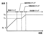
- FIG. It is a conceptual diagram of the crystal growth apparatus used by HVPE method. It is a conceptual diagram of the crystal growth apparatus used by the ammonothermal method.
- FIG. 6 is a schematic diagram showing a growth state of a GaN crystal on a ⁇ C plane (N polarity plane) of a C-plane GaN substrate on which a mask pattern having a line-shaped opening is formed. It is an example of the temperature profile which can be employ
- the surface of the nitride semiconductor single crystal is divided into a polar plane, a nonpolar plane, and a semipolar plane.
- the polar plane is a general term for the + C plane and the ⁇ C plane.
- the + C plane means a surface whose angle between the normal vector and the [0001] direction is 0 to 10 °.
- the ⁇ C plane means a surface whose normal vector has an angle of 0 to 10 ° with the [000-1] direction.
- the + C plane is a Ga polar plane and the ⁇ C plane is an N polar plane.
- the nonpolar plane is a general term for the M plane and the A plane.
- the M plane means a surface whose angle between the normal vector and the ⁇ 10-10> direction is 0 to 10 °.
- the A plane means a plane whose normal vector has an angle of 0 to 10 ° with the ⁇ 11-20> direction.
- the semipolar surface means a surface that does not correspond to either a polar surface or a nonpolar surface.
- the normal vectors thereof are ⁇ 30-31> direction, ⁇ 30-3-1> direction, ⁇ 20-21> direction, ⁇ 20-1-1> direction, and ⁇ 10-11> direction.
- ⁇ 10-1-1> direction ⁇ 10-12> direction, ⁇ 10-1-2> direction, ⁇ 10-13> direction, ⁇ 10-1-3> direction, ⁇ 11-21> direction
- ⁇ Includes a surface parallel to a direction selected from the 11-2-1> direction, the ⁇ 11-22> direction, the ⁇ 11-2-2> direction, the ⁇ 11-23> direction, and the ⁇ 11-2-3> direction. However, it is not limited.
- FIG. 1 shows a shape that a single crystal substrate such as a GaN substrate or a sapphire substrate or a composite substrate such as a GaN template normally has.
- the shape of the substrate 1 is a disc, that is, a plate having a circular main surface.
- substrate 1 is a board which has a rectangular main surface.
- the substrate 1 has two main surfaces 11 and end surfaces 12 that are parallel to each other. Chamfering for smoothing the boundary between the main surface 11 and the end surface 12 can be performed as necessary.
- the substrate can be provided with an orientation flat for displaying the crystal orientation and an index flat for identifying the front and back surfaces as necessary. .
- the nonpolar GaN substrate means a GaN substrate having a main surface which is a nonpolar surface.
- the semipolar GaN substrate means a GaN substrate having a main surface that is a semipolar surface.
- the M-plane GaN substrate referred to in this specification means a GaN substrate having a main surface that is an M-plane. Therefore, the M-plane substrate includes a just substrate in which the angle between the normal of the main surface and the ⁇ 1-100> direction of the GaN crystal is 0 °, and the normal of the main surface is ⁇ 1- The substrate with an off angle whose angle formed with the 100> direction is 10 ° or less is included.
- the C-plane GaN substrate referred to in this specification means a GaN substrate having a main surface that is a C-plane. Therefore, the C-plane substrate includes a just substrate whose angle between the normal of the main surface and the [0001] direction of the GaN crystal is 0 °, and the normal of the main surface is the [0001] direction of the GaN crystal. An off-angled substrate having an angle of 10 ° or less is included.
- the C-plane GaN substrate has one main surface serving as a + C plane and the other main surface serving as a -C plane because of the inherent properties of GaN crystals.
- the first main surface has a second main surface opposite to the first main surface, and the first main surface is a nonpolar surface or a semipolar surface,
- a nonpolar or semipolar GaN substrate having an average basal plane dislocation density of 1 ⁇ 10 6 cm ⁇ 2 or less in an arbitrary 250 ⁇ m square region in the first main surface is provided (Embodiment) 1).
- the basal plane dislocation density of the first main surface is calculated by excluding the damaged region. (Hereinafter, the same applies when referring to the basal plane dislocation density of the first main surface).
- the basal plane dislocation density can be measured using a transmission electron microscope (TEM), SEM-CL method (a method combining a scanning electron microscope and cathodoluminescence), and the number of pits formed by etching the sample surface. It can be measured by a method of observing with an AFM or an optical microscope.
- TEM transmission electron microscope
- SEM-CL method a method combining a scanning electron microscope and cathodoluminescence
- the basal plane dislocation density can be measured using a transmission electron microscope (TEM), SEM-CL method (a method combining a scanning electron microscope and cathodoluminescence), and the number of pits formed by etching the sample surface. It can be measured by a method of observing with an AFM or an optical microscope.
- the basal plane dislocation density averaged over the entire first main surface is 7 ⁇ 10 5 cm ⁇ 2 or less, further 5 ⁇ 10 5 cm ⁇ 2 or less, 2 ⁇ 10 5 cm ⁇ 2 or less, further 1 ⁇ 10 5 cm ⁇ 2 or less, further 1 ⁇ 10 4 cm ⁇ 2 or less, further 1 ⁇ 10 3 cm ⁇ 2 or less, further 10 cm ⁇ 2 or less, further Is more preferably 0 cm ⁇ 2 .
- the basal plane dislocation density averaged over the entire first main surface is 1 ⁇ 10 4 cm ⁇ 2 or less
- the basal plane averaged in the region in an arbitrary 250 ⁇ m square region in the first main surface is preferably 1 ⁇ 10 4 cm ⁇ 2 or less.
- the stacking fault density averaged over the entire first main surface is preferably 10 cm ⁇ 1 or less, more preferably 5 cm ⁇ 1 or less, and even more preferably 1 cm ⁇ 1 or less. is there.
- Stacking faults appearing on the main surface of the substrate propagate to the nitride semiconductor crystal that grows epitaxially on the main surface.
- the stacking fault density of the nonpolar or semipolar GaN substrate can be evaluated by low-temperature cathodoluminescence (LTCL) measurement performed by cooling the sample with liquid nitrogen.
- the stacking fault density cannot be evaluated by cathodoluminescence measurement at room temperature.
- the basal plane dislocation density on the second main surface opposite to the first main surface is not particularly limited.
- the GaN substrate according to Embodiment 1 is a non-metallic element other than nitrogen (N) and rare gas elements (He and Ne) belonging to the first period or the second period of the periodic table, that is, hydrogen (H), carbon ( C), oxygen (O) and fluorine (F) may be contained.
- the total concentration of these elements may exceed 1 ⁇ 10 17 cm ⁇ 3 , but preferably does not exceed 1 ⁇ 10 20 cm ⁇ 3 .
- the GaN substrate according to Embodiment 1 may contain silicon (Si), and the concentration thereof may be 1 ⁇ 10 17 cm ⁇ 3 or more, and further 5 ⁇ 10 17 cm ⁇ 3 or more.
- the silicon concentration of the GaN substrate according to Embodiment 1 is preferably 1 ⁇ 10 19 cm ⁇ 3 or less.
- the GaN substrate according to Embodiment 1 preferably has a low alkali metal concentration.
- the alkali metal concentration of the GaN substrate according to Embodiment 1 is 1 ⁇ 10 17 cm ⁇ 3 or less, further 5 ⁇ 10 16 cm ⁇ 3 or less, further 1 ⁇ 10 16 cm ⁇ 3 or less, and further 1 ⁇ 10 15. More preferably, it is not more than cm ⁇ 3 .
- the GaN substrate according to Embodiment 1 may contain point defects.
- the area of the first main surface is usually 1 cm 2 or more, preferably 2 cm 2 or more, more preferably 5 cm 2 or more, and may be 10 cm 2 or more.
- the GaN substrate according to Embodiment 1 is not limited, but can be manufactured by the following procedure.
- a secondary substrate is used as a seed, a GaN crystal is grown by an ammonothermal method, and the GaN crystal is processed to produce a nonpolar or semipolar GaN substrate (GaN substrate according to Embodiment 1). . Details of each step will be described below.
- a GaN crystal for a primary substrate is grown by HVPE using a C-plane GaN template in which a mask pattern for selective growth is previously formed on the surface of the GaN layer as a seed.
- the C-plane GaN template is a composite substrate having a single crystal substrate having a chemical composition different from that of GaN as a base material and a single crystal GaN layer grown on the c-axis on one main surface thereof.
- the surface of the single crystal GaN layer is the + C plane of GaN.
- the base material of the C-plane GaN template is a sapphire substrate, SiC substrate, Si substrate, Ga 2 O 3 substrate, AlN substrate, or the like.
- the single crystal GaN layer is formed by MOCVD and has a thickness of 0.5 to 100 ⁇ m, for example.
- the mask pattern is formed of a thin film made of a material that inhibits vapor phase growth of GaN, such as silicon nitride (SiN x ) or silicon oxide (SiO 2 ).
- a preferred example of the mask pattern is a stripe pattern (line & space pattern).
- the line width (mask width) in the stripe pattern can be 20 ⁇ m to 100 ⁇ m, and the space width can be 200 ⁇ m to 3000 ⁇ m.
- the direction of the stripe is parallel to the m-axis of the single crystal GaN layer.
- a crystal growth apparatus 2 shown in FIG. 2 includes a growth furnace 200, introduction pipes 201 to 205 for introducing gas into the growth furnace, a reservoir 206 for holding metal gallium, a heater 207 disposed so as to surround the growth furnace, A susceptor 208 for mounting the seed substrate and an exhaust pipe 209 for discharging gas from the inside of the growth furnace are provided.
- the material of the growth furnace 200, the introduction pipes 201 to 205, the reservoir 206, and the exhaust pipe 209 is preferably quartz.
- the material of the susceptor 208 is preferably carbon, and a material whose surface is coated with SiC is particularly preferable.
- the gases G1, G2, G4, and G5 introduced into the growth furnace 200 through the introduction pipes 201, 202, 204, and 205 are ammonia (NH 3 ), carrier gas, shield gas, doping gas, and the like.
- Hydrogen chloride (HCl) supplied to the reservoir 206 through the introduction pipe 203 reacts with metallic gallium held in the reservoir to generate gaseous gallium chloride (GaCl). Since HCl is usually diluted with a carrier gas and supplied to the reservoir 206, the gas G3 introduced into the growth reactor through the reservoir contains GaCl, HCl, and a carrier gas.
- Hydrogen gas (H 2 ) and nitrogen gas (N 2 ) are preferably used as the carrier gas and shield gas.
- GaN produced by the reaction of GaCl and NH 3 in the growth furnace 200 grows epitaxially on the seed substrate.
- the substrate temperature during crystal growth can be suitably adjusted, preferably in the range of 900 to 1200 ° C.
- the pressure in the growth furnace at the time of crystal growth can be suitably adjusted preferably within a range of 50 to 120 kPa.
- the susceptor 208 is preferably rotated so that crystals grow uniformly on the seed substrate.
- the rotation speed can be set to 1 to 50 rpm, for example.
- the crystal growth rate can be adjusted, for example, within a range of 80 to 300 ⁇ m / h.
- the growth rate can be increased by increasing the partial pressure of either or both of GaCl and NH 3 in the growth furnace.
- the GaCl partial pressure is preferably 2 ⁇ 10 2 to 2 ⁇ 10 3 Pa.
- the NH 3 partial pressure is preferably 4 ⁇ 10 3 to 1 ⁇ 10 4 Pa.
- the gas partial pressure referred to here is obtained by multiplying the pressure (P) in the growth furnace by the ratio (r) of the volume flow rate of the gas in the total volume flow rate of all the gases supplied into the growth furnace.
- the value (P ⁇ r) shall be said. The same applies when referring to the gas partial pressure in the growth furnace in the HVPE method.
- a GaN crystal for a secondary substrate is grown by an ammonothermal method using a primary substrate (C-plane GaN substrate) as a seed.
- a mask pattern for selective growth is formed on the ⁇ C plane (N polarity plane) of the primary substrate.
- the mask pattern is provided with a line-shaped opening having a width of about 100 ⁇ m and parallel to the a-axis of GaN.
- the mask is a metal that does not dissolve or decompose during the growth of the GaN crystal by the ammonothermal method, such as Al, W, Mo, Ti, Pt, Ir, Ag, Au, Ta, Ru, Nb, Pd, and alloys thereof. Form with.
- the raw material of GaN grown on the seed is preferably polycrystalline GaN, but is not limited and may contain metallic gallium (zero-valent gallium).
- metallic gallium zero-valent gallium
- the polycrystalline GaN there can be used those produced by a method of reacting metal gallium, gallium oxide, gallium hydroxide or the like with ammonia, or those produced by a method of reacting metal gallium with nitrogen under high temperature and high pressure.
- the concentration of oxygen contained as an impurity in polycrystalline GaN is usually 5 ⁇ 10 20 cm ⁇ 3 or less, preferably 1 ⁇ 10 20 cm ⁇ 3 or less, more preferably 5 ⁇ 10 19 cm ⁇ 3 or less.
- the amount of impurities such as water and oxygen contained in the ammonia used for the solvent is preferably 10 ppm or less, more preferably 0.1 ppm or less.
- the mineralizer those containing a halogen element such as ammonium halide, gallium halide, and hydrogen halide can be preferably used.
- the purity of the mineralizer is preferably 99% or more, more preferably 99.99% or more.
- Crystal growth is performed in a cylindrical growth vessel 320 loaded in a cylindrical autoclave 301.
- the growth vessel 320 has a crystal growth region 306 and a raw material dissolution region 309 that are partitioned by a baffle 305 inside.
- a seed crystal 307 suspended by a platinum wire 304 is installed in the crystal growth region 306.
- a raw material 308 is loaded in the raw material melting region 309.
- a gas line to which a vacuum pump 311, an ammonia cylinder 312 and a nitrogen cylinder 313 are connected is connected to the autoclave 301 via a valve 310.
- a growth vessel 320 filled with seed crystals, raw materials, a mineralizer and a solvent is loaded into the autoclave 301, and the solvent is also filled in the space between the autoclave 301 and the growth vessel 320.
- the autoclave 301 is sealed.
- the autoclave 301 is heated by a heater (not shown) to bring the inside of the growth vessel 320 into a supercritical state or a subcritical state.
- the pressure in the growth vessel 320 during crystal growth is usually 120 MPa or more, preferably 150 MPa or more, more preferably 180 MPa or more, and usually 700 MPa or less, preferably 500 MPa or less, more preferably 350 MPa or less, and 300 MPa or less. It may be.
- the temperature in the growth vessel 320 during crystal growth is usually 500 ° C. or higher, preferably 515 ° C. or higher, more preferably 530 ° C. or higher, and usually 700 ° C. or lower, preferably 650 ° C. or lower, more preferably 630 ° C. It is as follows.
- the raw material melting region 309 is set at a higher temperature than the crystal growth region 306.
- the temperature difference between the raw material dissolution region and the crystal growth region is preferably 5 ° C. or more, more preferably 10 ° C. or more, and preferably 100 ° C. or less, more preferably 80 ° C. or less.
- a plate-like GaN crystal having a thickness direction in the m-axis direction grows from the opening of the mask pattern.
- a secondary substrate M-plane GaN substrate
- the main surface used for epitaxial growth in the next step is flattened by lapping and subsequent CMP.
- CMP cross-sectional SEM-CL observation of the GaN crystal sliced and lapped under the same conditions is performed, and the approximate thickness of the damaged layer to be removed Is determined in advance, and the CMP amount is set in consideration of the thickness.
- a GaN crystal is grown by an ammonothermal method.
- the raw material, solvent, and mineralizer that can be preferably used in the case of using the ammonothermal method are the same as those for growing a GaN crystal for a secondary substrate.
- the crystal growth apparatus that can be used and preferable conditions for crystal growth are the same as those for growing a GaN crystal for a secondary substrate.
- the nonpolar or semipolar GaN substrate according to the first embodiment is cut out from the GaN crystal grown on the secondary substrate.
- An M-plane GaN substrate can be obtained by slicing parallel to the main surface of the secondary substrate.
- a GaN substrate having a non-polar surface other than the M-plane and various semipolar surfaces as the main surface can be obtained.
- at least one main surface is planarized by lapping and subsequent CMP.
- CMP cross-sectional SEM-CL observation of the GaN crystal sliced and lapped under the same conditions is performed, and the approximate thickness of the damaged layer to be removed Is determined in advance, and the CMP amount is set in consideration of the thickness.
- Nonpolar or Semipolar GaN Substrate A high-quality nitride semiconductor crystal with few stacking faults is formed by epitaxial growth on the first main surface having a low basal plane dislocation density of the GaN substrate according to Embodiment 1. be able to.
- the nonpolar or semipolar GaN substrate according to the first embodiment and the nitride semiconductor layer grown immediately above the first main surface of the substrate satisfy the condition of the lattice mismatch degree expressed by the following formula (1). It is preferable.
- a 1 and a 2 represent the lattice constants of crystal axes of GaN and the nitride semiconductor layer parallel to the first main surface, respectively.
- the lattice mismatch degree is more preferably 5 ⁇ 10 ⁇ 4 or less, further preferably 1 ⁇ 10 ⁇ 4 or less, and particularly preferably 1 ⁇ 10 ⁇ 5 or less.
- Various semiconductor device structures can be formed by epitaxially growing a nitride semiconductor on the first main surface of the GaN substrate according to the first embodiment.
- semiconductor devices include light-emitting devices such as light-emitting diodes and laser diodes, rectifiers, bipolar transistors, field-effect transistors, electronic devices such as HEMT (High Electron Mobility Transistor), temperature sensors, pressure sensors, radiation sensors, and visible- There are semiconductor sensors such as ultraviolet light detectors, SAW (Surface Acoustic Wave) devices, vibrators, resonators, oscillators, MEMS (Micro Electro Mechanical System) parts, voltage actuators, and the like.
- Bulk GaN crystals can also be epitaxially grown on the first main surface of the GaN substrate according to the first embodiment. That is, the GaN substrate according to Embodiment 1 can be used as a seed for growing a bulk GaN crystal.
- the semiconductor device further includes a first main surface and a second main surface opposite to the first main surface, the first main surface is an M plane, and an n-type impurity concentration is 4 ⁇ 10 18 cm.
- Embodiments 2a and 2b may be collectively referred to as Embodiment 2.
- the stacking fault density on the first main surface means the stacking fault density averaged over the entire first main surface.
- the stacking defect density of the first main surface is calculated by excluding the damaged region. (The same applies when referring to the stacking fault density of the first main surface below).
- the carrier concentration of the GaN substrate is 3 ⁇ 10 18 cm ⁇ 3 or more, an electrode having a low contact resistance can be easily formed on the surface.
- the carrier concentration of the GaN substrate is 4 ⁇ 10 18 cm ⁇ 3 or more, and further 5 ⁇ 10 18 cm ⁇ 3 or more, it becomes easier to form an electrode with low contact resistance on the surface.
- the carrier concentration of the M-plane GaN substrate according to Embodiment 2 is not particularly limited, but if it exceeds 1 ⁇ 10 19 cm ⁇ 3 , the effect of reducing the contact resistance with the electrode tends to be saturated. For example, in a light emitting device application, a carrier concentration exceeding 5 ⁇ 10 19 cm ⁇ 3 is rarely required for a GaN substrate.
- Known elements can be appropriately referred to as elements that can be added to GaN as impurities, and are not limited, but preferably include oxygen (O) and silicon (Si). Either one of oxygen and silicon may be used, or both may be used. In order to obtain a carrier concentration of 3 ⁇ 10 18 cm ⁇ 3 or more by using oxygen as an impurity, it is desirable that the oxygen concentration be 4 ⁇ 10 18 cm ⁇ 3 or more.
- the impurity concentration in the GaN substrate can be measured by SIMS (secondary ion mass spectrometry).
- the carrier concentration can be measured by Raman spectroscopy.
- the M-plane GaN substrate according to Embodiment 2 has a low stacking fault density on the first main surface of 100 cm ⁇ 1 or less, the MOCVD (metal organic chemical vapor deposition) method or the MBE (molecular beam epitaxy) method is used.
- MOCVD metal organic chemical vapor deposition
- MBE molecular beam epitaxy
- a high-quality nitride semiconductor thin film can be epitaxially grown on the first main surface.
- the stacking fault density on the first main surface is preferably 50 cm ⁇ 1 or less, more preferably 10 cm ⁇ 1 or less.
- the stacking fault density of the M-plane GaN substrate can be evaluated by low-temperature cathodoluminescence (LTCL) measurement performed by cooling the sample with liquid nitrogen.
- LTCL low-temperature cathodoluminescence
- the stacking fault density cannot be evaluated by cathodoluminescence measurement at room temperature.
- the M-plane GaN substrate according to Embodiment 2 can be manufactured from a GaN crystal grown by the HVPE method using the M-plane GaN substrate according to Embodiment 1 described above as a seed.
- the growth direction is a direction perpendicular to the main surface (M-plane) of the substrate.
- the growth direction is the thickness direction of the GaN crystal layer grown on the main surface of the substrate.
- the fluctuation of the oxygen concentration in the plane parallel to the main surface is less than 5 times.
- a plurality of seed substrates can be arranged like tiles on a susceptor, and one continuous GaN crystal layer can be grown on the plurality of seed substrates.
- the off angle of the main surface of the seed substrate is preferably 2 ° or more, and more preferably 5 ° or more.
- the growth of the GaN crystal by the HVPE method can be performed using the crystal growth apparatus whose conceptual diagram is shown in FIG.
- a GaN crystal having a reduced stacking fault density is obtained by performing a two-stage growth method including (a) a temperature raising step, (b) an initial growth step, and (c) a main growth step in this order, which will be described below. Obtainable.
- (A) Temperature raising step In the temperature raising step, the substrate temperature is raised from room temperature to T 1 without supplying GaCl to the seed substrate.
- T 1 is preferably 830 ° C. or higher and 870 ° C. or lower.
- the temperature rising rate is preferably 12 ° C./min or more and 30 ° C./min or less.
- the temperature increase rate may be constant over the entire period of the temperature increase step, or may be changed in the middle.
- the atmospheric gas that can be introduced into the growth furnace in the temperature raising step is H 2 , NH 3 , N 2 or the like, and it is preferable to introduce at least both NH 3 and N 2 .
- the volume flow rate of NH 3 introduced into the growth furnace is preferably 15% or more of the sum of the volume flow rates of all the gases introduced into the growth furnace.
- the substrate temperature is increased from T 1 to T 2 while GaCl and NH 3 are supplied to the seed substrate to grow a GaN crystal.
- T 2 is preferably 940 ° C. or higher and 1050 ° C. or lower.
- the temperature rising rate is preferably 11 ° C./min or more and 24 ° C./min or less.
- the growth furnace pressure in the initial growth step is 1.0 ⁇ 10 5 Pa
- the GaCl partial pressure is preferably 2.0 ⁇ 10 2 Pa or more and 5.0 ⁇ 10 2 Pa or less
- the NH 3 partial pressure is Is preferably 8.0 ⁇ 10 3 Pa or more and 1.2 ⁇ 10 4 Pa or less.
- N 2 occupies 70% or more, more preferably 90% or more of the volume flow rate of all the gases introduced into the growth furnace.
- H 2 can be introduced into the growth furnace in the initial growth step.
- (C) Main growth step In the main growth step, GaCl and NH 3 are supplied onto the seed substrate while maintaining the substrate temperature at T 2 to grow a GaN crystal into a thick film.
- the growth furnace pressure in the main growth step is preferably 50 kPa or more and 120 kPa or less.
- the GaCl partial pressure is preferably 2.0 ⁇ 10 2 Pa or more and 5.0 ⁇ 10 2 Pa or less
- the NH 3 partial pressure is Is preferably 8.0 ⁇ 10 3 Pa or more and 1.5 ⁇ 10 4 Pa or less.
- N 2 occupies 70% or more, more preferably 90% or more of the volume flow rate of all the gases introduced into the growth furnace.
- H 2 can be introduced into the growth furnace in the main growth step.
- the temperature increase rate is constant from the temperature increase step to the initial growth step.
- a temperature holding step for holding the substrate temperature constant is provided between the temperature raising step and the initial growth step.
- the period of the temperature holding step can be set as appropriate, and is, for example, 1 minute to 60 minutes.
- the temperature increase rate is changed between the first half and the second half of the initial growth step. In this example, the temperature increase rate is changed discontinuously, but can be changed gradually.
- a GaN crystal can be grown while supplying a doping gas.
- a doping gas for oxygen doping oxygen gas (O 2 ) or water (H 2 O) is used, and as a doping gas for silicon doping, silane (SiH 4 ), disilane (Si 2 H 6 ), chlorosilane (SiH 3 ). Cl), dichlorosilane (SiH 2 Cl 2 ), trichlorosilane (SiHCl 3 ), tetrachlorosilane (SiCl 4 ), tetrafluorosilane (SiF 4 ), and the like can be preferably used.
- a liner tube made of high-purity pBN pyrolytic boron nitride
- a seed substrate is placed inside the liner tube, so that the oxygen-containing gas generated from the quartz growth furnace is transferred to the seed substrate. Prevent contact.
- a susceptor on which the seed substrate is placed is provided with a local heating mechanism, and the seed substrate is heated by using the local heating mechanism and a heater in combination.
- the heater output necessary to heat the seed substrate to a predetermined temperature can be lowered, so that the temperature of the quartz member such as the growth furnace, the introduction tube, and the reservoir heated by the heater together with the seed substrate can be lowered.
- the amount of oxygen-containing gas generated from these quartz members can be suppressed.
- the temperature of the reservoir can be lowered, and consequently the amount of oxygen-containing gas generated from the reservoir can be suppressed.
- the GaN substrate according to Embodiment 2 can be preferably used for manufacturing a semiconductor light-emitting device such as a light-emitting diode (LED) or a laser diode (LD).
- FIG. 8 shows a structural example of a semiconductor light emitting device that can be manufactured using the GaN substrate according to the second embodiment.
- FIG. 8 is a cross-sectional view, and the semiconductor light emitting device 40A has a semiconductor stacked body L grown on the main surface of the GaN substrate 41 by the MOVPE method (organic metal compound vapor phase epitaxy).
- the semiconductor stacked body L includes an n-type layer 42, a light emitting layer 43, and a p-type layer 44 in this order from the GaN substrate 41 side.
- the n-type layer 42 is formed of, for example, GaN or AlGaN, and is doped with Si.
- the light emitting layer 43 is formed by, for example, alternately laminating In x1 Ga 1-x1 N well layers and In x2 Ga 1-x2 N (0 ⁇ x2 ⁇ x1) barrier layers.
- the p-type layer 44 is formed of, for example, GaN or AlGaN, and is doped with Mg.
- a positive electrode 45 is formed on the upper surface of the p-type layer 44.
- a negative electrode 46 is formed on the surface of the n-type layer exposed by partial etching of the stacked body.
- the quality of the semiconductor stacked body L grown on the GaN substrate 41 is improved, and the light emitting efficiency of the semiconductor light emitting device 40A is improved.
- the n-type carrier concentration of the GaN substrate 41 By increasing the n-type carrier concentration of the GaN substrate 41, its electrical resistance is lowered and it works as a current path together with the n-type layer 42, so that the operating voltage of the semiconductor light emitting device 40A is reduced.
- the semiconductor light emitting device 40B having the negative electrode 46 on the back surface of the GaN substrate 41 shown in FIG. 9 the effect of reducing the operating voltage by increasing the carrier concentration of the GaN substrate 41 becomes more remarkable. This is because the contact resistance between the negative electrode 46 and the GaN substrate 41 decreases due to the increase in the carrier concentration of the GaN substrate 41 in addition to the decrease in the series resistance of the device due to the decrease in the electrical resistance of the GaN substrate 41.
- a GaN layer bonded substrate can be manufactured.
- a GaN layer bonded substrate is a composite substrate in which a GaN layer is bonded to a different composition substrate having a different chemical composition from GaN, and is used for manufacturing light emitting devices and other semiconductor devices. can do.
- the GaN layer bonded substrate is typically ion-implanted with a first step of implanting ions in the vicinity of the main surface of the GaN substrate, a second step of bonding the main surface side of the GaN substrate to the different composition substrate, and By separating the GaN substrate with the region as a boundary, the third step of forming the GaN layer bonded to the different composition substrate can be manufactured by executing in this order. Therefore, the GaN layer bonded substrate manufactured using the GaN substrate according to the second embodiment has a structure in which the GaN layer separated from the GaN substrate according to the second embodiment is bonded to the different composition substrate. .
- the M-plane GaN substrate according to Embodiment 2 can be used as a substrate for manufacturing various semiconductor devices as well as light-emitting devices.
- electronic devices such as rectifiers, bipolar transistors, field effect transistors, and high electron mobility transistors (HEMTs)
- semiconductor sensors such as temperature sensors, pressure sensors, radiation sensors, and visible-ultraviolet light detectors, and surface acoustic wave (SAW) devices
- SAW surface acoustic wave
- Vibrators Vibrators, resonators, oscillators, MEMS (Micro Electro Mechanical System) parts, voltage actuators, and the like.
- MEMS Micro Electro Mechanical System
- a GaN crystal was grown by an ammonothermal method using the prepared primary substrate as a seed.
- the specific procedure is as follows.
- ammonium fluoride (NH 4 F) and hydrogen iodide (HI) were prepared as mineralizers.
- NH 4 F ammonium fluoride
- HI hydrogen iodide
- a mask pattern having a line-shaped opening having a width of 100 ⁇ m was formed of a TiW alloy. The longitudinal direction of the opening was parallel to the a-axis of GaN.
- the autoclave was heated from the outside using an electric furnace equipped with a plurality of independently controllable heaters. Hold the heater for 30 days by controlling the heater so that the average temperature in the growth vessel (the average temperature of the crystal growth region and the raw material dissolution region) is 600 ° C., and the temperature difference between the crystal growth region and the raw material dissolution region is 20 ° C. did. At this time, the pressure in the autoclave was 215 MPa.
- the autoclave valve is opened to release the NH 3 filled in the space between the growth vessel and the autoclave, and the pressure difference generated inside and outside the growth vessel is utilized. Cracked the growth vessel. Then, after confirming that NH 3 in the growth vessel was also discharged, the primary substrate was taken out. On the ⁇ C plane of the primary substrate taken out from the growth vessel, a plate-like GaN crystal having a dimension in the c-axis direction of 7 mm and a thickness direction in the m-axis direction was grown from the opening of the mask pattern.
- a 35 mm (length) ⁇ 7 mm (width) ⁇ 330 ⁇ m (thickness) M-plane substrate (2) having a rectangular main surface whose long side is parallel to the a axis and whose short side is parallel to the c axis. Next substrate) was cut out. Both main surfaces were lapped and subjected to CMP treatment to completely remove the damaged layer formed by slicing.
- tertiary substrate (M-plane GaN substrate) Using the secondary substrate (M-plane GaN substrate) produced by the above procedure as a seed, a GaN crystal was grown by an ammonothermal method. The seeds were different, the amount of the mineralizer charged was changed so that the molar ratio of fluorine atom and iodine atom to NH 3 was 0.5% and 1.5%, respectively, and the crystal growth time was 20 days. Except for the above, a GaN crystal for a tertiary substrate was grown in the same procedure as when a GaN crystal for a secondary substrate was grown.
- the size of the GaN crystal obtained by the growth for 20 days was 40 mm (a-axis direction) ⁇ 10 mm (c-axis direction) ⁇ 6 mm (m-axis direction). From this GaN crystal, an M surface with an off-angle of 17 mm (length) ⁇ 8 mm (width) ⁇ 330 ⁇ m (thickness) having a rectangular main surface whose long side is parallel to the a axis and whose short side is parallel to the c axis A substrate (tertiary substrate) was cut out. The off angle was set to -2 ° in the [0001] direction, and the [-12-10] direction was within ⁇ 0.1 °.
- the stacking fault density of this substrate was 0 cm ⁇ 1 .
- the observation area per field of view was 90 ⁇ m ⁇ 120 ⁇ m for a 1000 ⁇ field and 600 ⁇ m ⁇ 400 ⁇ m for a 200 ⁇ field.
- GaN Crystal Growth by HVPE Method A GaN crystal was grown by the HVPE method using the tertiary substrate (M-plane GaN substrate) produced by the above procedure as a seed substrate.
- the above-described two-stage growth method was used. That is, after placing the seed substrate on a susceptor installed in the growth furnace so that one main surface is facing upward, the substrate temperature is first adjusted while supplying only N 2 and NH 3 to the seed substrate. The temperature was raised to 850 ° C. (temperature raising step) and held at this temperature for 15 minutes. Next, by supplying HCl diluted with N 2 to a reservoir heated to 800 ° C.
- GaCl GaCl
- NH 3 GaN crystal
- the pressure in the growth furnace is 1.0 ⁇ 10 5 Pa
- the partial pressure of GaCl is 3.1 ⁇ 10 2 Pa
- the partial pressure of ammonia is 9.8 ⁇ 10.
- Control was performed to 3 Pa.
- N 2 and H 2 were used as the carrier gas, and the ratio of N 2 in the total volume flow rate of all the gases supplied into the growth furnace was 48%.
- the grown GaN crystal covered the main surface of the tertiary substrate in a film shape, and the thickness was about 0.8 mm.
- the basal plane dislocation density was 9.4 ⁇ 10 5 cm ⁇ 2 .
- a low-temperature cathodoluminescence method acceleration voltage 5 kV, current 500 pA, 200-fold field of view, sample temperature 82 K
- the oxygen concentration of the azuron GaN crystal film measured by SIMS analysis was 4.0 ⁇ 10 18 cm ⁇ 3
- the carrier concentration near the main surface measured by Raman spectroscopy was 2.5 ⁇ 10 18 cm ⁇ . 3 .
- This oxygen concentration value was lower than the oxygen concentration (8.7 ⁇ 10 18 cm ⁇ 3 ) of the tertiary substrate used for the seed, and the difference was 4.7 ⁇ 10 18 cm ⁇ 3 .
- the oxygen contained in the GaN crystal film was considered to be derived from an oxygen compound such as H 2 O mixed in the raw material or a quartz member constituting the vapor phase growth apparatus.
- a C-plane GaN template is prepared by growing a single crystal GaN layer on a C-plane sapphire substrate, and silicon nitride with a thickness of 80 nm is formed on the surface of the GaN layer.
- a mask pattern was formed with the film.
- a plasma CVD method was used for forming the silicon nitride film, and photolithography and dry etching techniques were used for patterning.
- the mask pattern was a 850 ⁇ m pitch stripe pattern (line & space pattern) with a line width (mask width) of 50 ⁇ m and a space width of 800 ⁇ m, and the stripe direction was parallel to the m-axis of the single crystal GaN layer.
- An undoped GaN crystal was grown by the HVPE method on the C-plane GaN template on which the mask pattern was formed.
- the substrate temperature was increased to 970 ° C. for 15 minutes after the start of growth, and then the substrate temperature was increased to 1020 ° C. to continue the growth.
- the pressure in the growth furnace was controlled to 1.0 ⁇ 10 5 Pa
- the GaCl partial pressure was 7.4 ⁇ 10 2 Pa
- the ammonia partial pressure was 1.1 ⁇ 10 4 Pa.
- the growth time was 55 hours.
- a C-plane substrate (primary substrate) having a thickness of 330 ⁇ m was cut out from the GaN crystal thus grown.
- the ⁇ C surface was subjected to lapping and CMP treatment to completely remove the damaged layer formed by slicing.
- a mask pattern having a line-shaped opening with a width of 100 ⁇ m parallel to the a-axis of GaN is formed on the ⁇ C plane of the C-plane GaN substrate produced by the above procedure.
- a GaN crystal was grown by an ammonothermal method using the material formed in (1) as a seed. Growth of a GaN crystal by the ammonothermal method and production of a tertiary substrate (M-plane substrate) from the GaN crystal resulted in a molar ratio of fluorine atoms to iodine atoms of 0.5% and 0.75%, respectively.
- a GaN crystal was grown by an ammonothermal method using the M-plane GaN substrate produced by the above procedure as a seed. Using different seed crystals, changing the amount of mineralizer charged so that the molar ratio of fluorine and iodine atoms to ammonia was 0.5% and 1.5%, respectively, and the crystal growth time.
- a GaN crystal for a tertiary substrate was grown in the same procedure as that for growing a GaN crystal for a secondary substrate, except for 16 days.
- the size of the obtained GaN crystal was 32 mm (a-axis direction) ⁇ 12 mm (c-axis direction) ⁇ 6 mm (m-axis direction).
- a substrate was cut out.
- the off angle was set to -2 ° in the [0001] direction, and the [-12-10] direction was within ⁇ 0.1 °. Both main surfaces were lapped and subjected to CMP treatment to completely remove the damaged layer formed by slicing.
- the oxygen concentration was 2.3 ⁇ 10 18 cm ⁇ 3 .
- no basal plane dislocation was detected in the analysis by the room temperature cathodoluminescence method (3 kV, 100 pA, 1000 ⁇ field of view).
- the stacking fault density of this substrate was 0 cm ⁇ 1 .
- GaN Crystal Growth by HVPE Method A GaN crystal was grown by the HVPE method using the tertiary substrate (M-plane GaN substrate) produced by the above procedure as a seed substrate.
- M-plane GaN substrate tertiary substrate
- the angle formed by the a-axis of each seed substrate when the susceptor is viewed from above is set to be within 0.5 °.
- the aforementioned two-stage growth method was used for the growth of the GaN crystal. That is, after placing the seed substrate in the growth furnace, the substrate temperature is first raised to 850 ° C.
- the pressure in the growth furnace is 1.0 ⁇ 10 5 Pa
- the partial pressure of GaCl is 3.8 ⁇ 10 2 Pa
- the partial pressure of ammonia is 1.2 ⁇ 10. Control was performed to 4 Pa.
- N 2 and H 2 were used as the carrier gas, and the ratio of N 2 in the total volume flow rate of all the gases supplied into the growth furnace was 48%.
- the grown GaN crystal had a continuous film shape from one seed substrate to the other seed substrate, and its thickness was about 5.1 mm. From this GaN crystal, it has a rectangular main surface whose long side is parallel to the a-axis and whose short side is parallel to the c-axis, and is 25.5 mm (length) ⁇ 12.5 mm (width) ⁇ 354 ⁇ m (thickness) off A cornered M-plane substrate was cut out. The off-angle was ⁇ 5 ° in the [0001] direction, and the [-12-10] direction was within ⁇ 0.1 °. Both main surfaces were lapped and subjected to CMP treatment to completely remove the damaged layer formed by slicing.
- the basal plane dislocation density and stacking fault density on the main surface were measured.
- the basal plane dislocation density measured by the room temperature cathodoluminescence method (acceleration voltage 7 kV, current 2 nA, 1000 ⁇ field of view) was 3.1 ⁇ 10 5 cm ⁇ 2
- the low temperature cathodoluminescence method (acceleration voltage 7 kV, current 2 nA).
- the stacking fault density was 1.8 cm ⁇ 1 measured at 200 ⁇ field of view and sample temperature of 82K.
- the carrier concentration in the vicinity of the main surface measured by Raman spectroscopy of this M-plane GaN substrate was 5.8 ⁇ 10 18 to 1.3 ⁇ 10 19 cm ⁇ 3 .
- the origin of the carrier was thought to be oxygen incorporated into the GaN crystal during vapor phase growth.
- a C-plane GaN template was prepared by growing a single crystal GaN layer on a sapphire substrate by metal organic chemical deposition (MOCVD).
- MOCVD metal organic chemical deposition
- a mask pattern for selective growth composed of a silicon nitride film having a thickness of 80 nm and exhibiting a superposition of a dot pattern and a triangular lattice pattern was formed.
- the dot pattern included in the superposition pattern was a pattern in which regular hexagonal dots were arranged at each lattice position of a square lattice having a square having a side of 800 ⁇ m as a unit lattice.
- the square lattice was oriented so that the two sides of the unit cell square were parallel to the a-axis of the GaN layer and the other two sides were parallel to the m-axis of the GaN layer.
- Each dot was arranged so that each side of the regular hexagon was parallel to the m-axis of the GaN layer.
- the size of each dot was determined so that the distance between two parallel sides of the regular hexagon was 100 ⁇ m, that is, the length of one side of the regular hexagon was 57.7 ⁇ m.
- the triangular lattice pattern included in the superposed pattern had a line width W of 2 ⁇ m and a regular triangle height obtained by connecting adjacent lattice points to 20 ⁇ m.
- the lattice pitch (distance between two adjacent lattice points) P was 23.1 ⁇ m.
- the triangular lattice pattern was oriented so that each line constituting the triangular lattice was parallel to the a-axis of the GaN layer.
- a GaN crystal was grown by the HVPE method on the C-plane GaN template on which the selective growth mask was formed.
- the growth temperature was 965 ° C. for the first 15 minutes and then increased to 1005 ° C.
- the growth pressure was 1.0 ⁇ 10 5 Pa
- the GaCl partial pressure was 1.0 ⁇ 10 3 Pa
- the NH 3 partial pressure was 1.0 ⁇ 10 4 Pa.
- the growth time was 51 hours. Due to the occurrence of the facet growth mode, the growing GaN crystal was doped with oxygen. Oxygen was thought to be derived from oxygen compounds such as H 2 O mixed in the raw material or quartz members constituting the vapor phase growth apparatus.
- the thickness of the azugron GaN crystal was 9.9 mm, and its surface had irregularities, indicating that facet growth was maintained.
- the radius of curvature of the (0001) plane of the as-gron crystal examined by X-ray diffraction analysis was 59 m in the a-axis direction and 13 m in the m-axis direction.
- the obtained GaN crystal has an oblong angle of 30 mm (length) ⁇ 5 mm (width) ⁇ 330 ⁇ m (thickness) having a rectangular main surface whose long side is parallel to the a axis and whose short side is parallel to the c axis.
- the M-plane substrate was cut out.
- the off-angle was ⁇ 5 ° in the [0001] direction, and the [-12-10] direction was within ⁇ 0.1 °. Both main surfaces were lapped and subjected to CMP treatment to completely remove the damaged layer formed by slicing.
- a GaN crystal was grown by HVPE method.
- the above-described two-stage growth method was used. That is, after placing the seed substrate on a susceptor installed in the growth furnace so that one main surface is facing upward, the substrate temperature is first adjusted while supplying only N 2 and NH 3 to the seed substrate. The temperature was raised to 850 ° C. (temperature raising step) and held at this temperature for 15 minutes. Next, by supplying HCl diluted with N 2 to a reservoir heated to 800 ° C.
- GaCl and NH 3 were supplied to the seed substrate while keeping the substrate temperature constant, and a GaN crystal was grown for 50 hours (main growth step). From the start of the heating step to the end of the main growth step, the pressure in the growth furnace is 1.0 ⁇ 10 5 Pa, the partial pressure of GaCl is 4.1 ⁇ 10 2 Pa, and the partial pressure of ammonia is 1.3 ⁇ 10. Control was performed to 4 Pa. N 2 and H 2 were used as the carrier gas, and the ratio of N 2 in the total volume flow rate of all the gases supplied into the growth furnace was 48%.
- the thickness of the obtained GaN crystal layer was about 4.0 mm.
- a plurality of off-angled M-plane substrates having a rectangular main surface with long sides parallel to the a-axis and short sides parallel to the c-axis were cut out from the GaN crystal.
- the off-angle was ⁇ 5 ° in the [0001] direction, and the [-12-10] direction was within ⁇ 0.1 °.
- the stacking fault density on the main surface (corresponding to a growth thickness of about 2 mm) was measured using the low-temperature cathodoluminescence method (acceleration voltage 7 kV, current 2 nA, 300 ⁇ field of view, sample temperature 82K). ) To be 27 cm ⁇ 1 .
- a GaN crystal was grown on the + C plane of the C-plane GaN substrate produced in (1) above by the HVPE method.
- the growth temperature was 1065 ° C. for the first 1 hour and 40 minutes and then lowered to 1005 ° C.
- the growth pressure was 1.0 ⁇ 10 5 Pa
- the GaCl partial pressure was 6.3 ⁇ 10 2 Pa
- the NH 3 partial pressure was 7.4 ⁇ 10 3 Pa.
- the total growth time was 20 hours.
- the thickness of the azugron GaN crystal was 3.0 mm, and the surface thereof was a mirror surface (C surface).
- the basal plane dislocation density on the main surface of the M-plane GaN substrate was evaluated by a room temperature cathodoluminescence method (3 kV, 100 pA, 1000-fold field of view), it was 1.0 ⁇ 10 4 cm ⁇ 2 or less.
- GaN crystal growth by HVPE method The GaN crystal was grown by the HVPE method using the secondary substrate produced in the above (2) as a seed substrate.
- the above-described two-stage growth method was used. That is, after placing the seed substrate on a susceptor installed in the growth furnace so that one main surface is facing upward, the substrate temperature is first adjusted while supplying only N 2 and NH 3 to the seed substrate. The temperature was raised to 850 ° C. (temperature raising step) and held at this temperature for 15 minutes. Next, by supplying HCl diluted with N 2 to a reservoir heated to 800 ° C.
- GaCl and NH 3 were supplied to the seed substrate while keeping the substrate temperature constant, and a GaN crystal was grown for 15 hours (main growth step). From the start of the heating step to the end of the main growth step, the pressure in the growth furnace is 1.0 ⁇ 10 5 Pa, the partial pressure of GaCl is 4.1 ⁇ 10 2 Pa, and the partial pressure of ammonia is 1.3 ⁇ 10. Control was performed to 4 Pa. N 2 and H 2 were used as the carrier gas, and the ratio of N 2 in the total volume flow rate of all the gases supplied into the growth furnace was 48%.
- the film thickness of the obtained GaN crystal layer was about 1.5 mm.
- the stacking fault density of the as-grown GaN crystal was evaluated by a low-temperature cathodoluminescence method (7 kV, 2 nA, 300 ⁇ field of view, sample temperature 82 K), it was 0 cm ⁇ 1 .
- Experiment 5 (1) Production of M-plane GaN substrate A C-plane GaN template was prepared by epitaxially growing a non-doped GaN layer on a sapphire substrate by MOCVD. Next, a mask pattern for selective growth was formed with a silicon nitride film on the surface of the GaN layer.
- the mask pattern was a 850 ⁇ m pitch stripe pattern (line & space pattern) with a line width (mask width) of 50 ⁇ m and a space width of 800 ⁇ m, and the stripe direction was parallel to the m-axis of the GaN layer.
- an undoped GaN layer was further laterally epitaxially grown by MOCVD to obtain a seed substrate.
- a GaN crystal was grown on the seed substrate by the HVPE method.
- the growth temperature was 1010 ° C.
- the growth pressure was 1.0 ⁇ 10 5 Pa
- the GaCl partial pressure was 6.6 ⁇ 10 2 Pa
- the NH 3 partial pressure was 7.6 ⁇ 10 3 Pa.
- the growth time was 64 hours.
- the thickness of the azugron GaN crystal was 8.3 mm. From this GaN crystal, an M-plane with an off angle of 50 mm (length) ⁇ 5 mm (width) ⁇ 330 ⁇ m (thickness) having a rectangular main surface whose long side is parallel to the a axis and whose short side is parallel to the c axis The substrate was cut out. The off-angle was ⁇ 5 ° in the [0001] direction, and the [-12-10] direction was within ⁇ 0.1 °. Wrapping and CMP treatment were performed on both surfaces to completely remove the damaged layer formed by slicing.
- a GaN crystal was grown by HVPE method.
- the above-described two-stage growth method was used. That is, after placing the seed substrate on the susceptor in the growth furnace, the substrate temperature was first raised to 850 ° C. while only N 2 and NH 3 were supplied to the seed substrate, and held at this temperature for 15 minutes. Next, by supplying HCl diluted with N 2 to a reservoir heated to 800 ° C. holding metallic gallium, supply of GaCl to the seed substrate is started, and the substrate temperature is set at a rate of 21 ° C./min. Was raised.
- the pressure in the growth furnace is 1.0 ⁇ 10 5 Pa
- the GaCl partial pressure is 3.5 ⁇ 10 2 Pa
- the NH 3 partial pressure is 1.1. ⁇ 10 4 Pa.
- the film thickness of the obtained GaN crystal layer was about 0.8 mm.
- the basal plane dislocation density of the as-gron GaN crystal was evaluated by a room temperature cathodoluminescence method (3 kV, 100 pA, 1000 ⁇ field of view), it was 1.5 ⁇ 10 6 cm ⁇ 2 .
- the stacking fault density of the as-gron GaN crystal was evaluated by a low temperature cathodoluminescence method (5 kV, 500 pA, 200 ⁇ field of view, sample temperature 82 K), and found to be 1.5 ⁇ 10 2 cm ⁇ 1 .
- Experiment 6 (1) Production of M-plane GaN substrate From a GaN crystal grown on a C-plane GaN template by the same method as in Experiment 5 (1), the long side is parallel to the a-axis and the short side is parallel to the c-axis. A 20 mm (length) ⁇ 10 mm (width) ⁇ 330 ⁇ m (thickness) M-plane just substrate (M-plane substrate without an off angle) having a rectangular main surface was cut out. Both main surfaces were lapped and subjected to CMP treatment to completely remove the damaged layer formed by slicing.
- a plurality of M-plane substrates were cut out from the GaN crystal. Wrapping and CMP treatment were performed on both main surfaces of the cut out substrate to completely remove the damaged layer formed by slicing.
- the stacking fault density on the main surface of this M-plane GaN substrate was 1.5 ⁇ 10 2 cm ⁇ 1 as measured by a low-temperature cathodoluminescence method (5 kV, 500 pA, 200 ⁇ field of view, sample temperature 82K).
- Table 1 summarizes the results of Experiments 1-6.
Abstract
The main purpose of the present invention is to provide: a nonpolar or semipolar GaN substrate, in which a nitride semiconductor crystal having a low stacking fault density can be epitaxially grown on the main surface of the substrate; and a technique required for the production of the substrate. A gallium nitride substrate having a first main surface and a second main surface that is located on the opposed side of the first main surface, wherein the first main surface is a nonpolar surface or a semipolar surface, and the average basal-plane dislocation density in arbitrary 250-μm square regions in the first main surface is 1 × 106 cm-2 or less.
Description
本発明は、窒化ガリウム基板、および、窒化物半導体結晶の製造方法に関する。
The present invention relates to a gallium nitride substrate and a method for manufacturing a nitride semiconductor crystal.
窒化ガリウム(GaN)に代表される窒化物半導体は、周期表の第13族に属する金属元素の窒化物で構成される半導体であり、III族窒化物系化合物半導体、窒化ガリウム系半導体などとも呼ばれる。窒化物半導体は、(B,Al,Ga,In)N、(Al,Ga,In)N、BxAlyGazIn1-x-y-zN(ただし、0≦x≦1,0≦y≦1,0≦z≦1,0≦x+y+z≦1)、AlxGayIn1-x-yN(ただし、0≦x≦1,0≦y≦1,0≦x+y≦1)などの組成式を用いて表記される場合がある。
不純物でドープすることにより、窒化物半導体は導電性とすることができる。O(酸素)、Si(ケイ素)、Ge(ゲルマニウム)などがn型不純物として知られている。Mg(マグネシウム)、Zn(亜鉛)などがp型不純物として知られている。
窒化物半導体は、六方晶系に属するウルツ鉱型の結晶構造を備える。 A nitride semiconductor typified by gallium nitride (GaN) is a semiconductor composed of a nitride of a metal element belonging to Group 13 of the periodic table, and is also referred to as a Group III nitride compound semiconductor, a gallium nitride semiconductor, or the like. . Nitride semiconductor, (B, Al, Ga, In) N, (Al, Ga, In) N, B x Al y Ga z In 1-x-y-z N ( However, 0 ≦ x ≦ 1,0 ≤ y ≤ 1, 0 ≤ z ≤ 1, 0 ≤ x + y + z ≤ 1), Al x Ga y In 1-xy N (where 0 ≤ x ≤ 1, 0 ≤ y ≤ 1, 0 ≤ x + y ≤ 1) In some cases, the composition formula is used.
By doping with impurities, the nitride semiconductor can be made conductive. O (oxygen), Si (silicon), Ge (germanium) and the like are known as n-type impurities. Mg (magnesium), Zn (zinc), etc. are known as p-type impurities.
Nitride semiconductors have a wurtzite crystal structure belonging to the hexagonal system.
GaN基板は、HVPE(Hydride Vapor Phase Epitaxy)法(特許文献1)やアモノサーマル法(特許文献2、特許文献3)により成長させたバルクGaN結晶をスライスする方法で製造される。
非極性または半極性GaN基板は、C面サファイア基板あるいはC面GaN基板上にc軸成長したバルクGaN結晶を、非極性面または半極性面が主表面として現われるようにスライスする方法で得ることが可能である(非特許文献1)。この方法は、積層欠陥密度が低い非極性または半極性GaN基板が得られる点で有利であるものの、大面積基板の製造には適していない。そこで、最近では非極性または半極性GaN基板をシードに用いたホモエピタキシャル成長により、バルクGaN結晶を製造することが検討されている(特許文献4)。 The GaN substrate is manufactured by a method of slicing a bulk GaN crystal grown by an HVPE (Hydride Vapor Phase Epitaxy) method (Patent Document 1) or an ammonothermal method (Patent Documents 2 and 3).
The nonpolar or semipolar GaN substrate can be obtained by slicing a bulk GaN crystal grown on the c-axis on a C-plane sapphire substrate or C-plane GaN substrate so that the nonpolar plane or the semipolar plane appears as a main surface. It is possible (Non-Patent Document 1). Although this method is advantageous in that a nonpolar or semipolar GaN substrate having a low stacking fault density is obtained, it is not suitable for manufacturing a large area substrate. Therefore, recently, it has been studied to produce a bulk GaN crystal by homoepitaxial growth using a nonpolar or semipolar GaN substrate as a seed (Patent Document 4).
非極性または半極性GaN基板は、C面サファイア基板あるいはC面GaN基板上にc軸成長したバルクGaN結晶を、非極性面または半極性面が主表面として現われるようにスライスする方法で得ることが可能である(非特許文献1)。この方法は、積層欠陥密度が低い非極性または半極性GaN基板が得られる点で有利であるものの、大面積基板の製造には適していない。そこで、最近では非極性または半極性GaN基板をシードに用いたホモエピタキシャル成長により、バルクGaN結晶を製造することが検討されている(特許文献4)。 The GaN substrate is manufactured by a method of slicing a bulk GaN crystal grown by an HVPE (Hydride Vapor Phase Epitaxy) method (Patent Document 1) or an ammonothermal method (
The nonpolar or semipolar GaN substrate can be obtained by slicing a bulk GaN crystal grown on the c-axis on a C-plane sapphire substrate or C-plane GaN substrate so that the nonpolar plane or the semipolar plane appears as a main surface. It is possible (Non-Patent Document 1). Although this method is advantageous in that a nonpolar or semipolar GaN substrate having a low stacking fault density is obtained, it is not suitable for manufacturing a large area substrate. Therefore, recently, it has been studied to produce a bulk GaN crystal by homoepitaxial growth using a nonpolar or semipolar GaN substrate as a seed (Patent Document 4).
特許文献4によれば、非極性または半極性GaN基板をシードに用いて、積層欠陥密度が100cm-1以下のGaN結晶をホモエピタキシャル成長させるには、成長させるGaN結晶とシードの間の不純物濃度差を3×1018cm-3以下にする必要があるとのことである。この文献には、不純物濃度4×1018cm-3以上かつ積層欠陥密度100cm-1以下のGaN結晶を、非極性GaN基板上にホモエピタキシャル成長させた例は記載されていない。
According to Patent Document 4, in order to homoepitaxially grow a GaN crystal having a stacking fault density of 100 cm −1 or less using a nonpolar or semipolar GaN substrate as a seed, the difference in impurity concentration between the GaN crystal to be grown and the seed Is required to be 3 × 10 18 cm −3 or less. This document does not describe an example in which a GaN crystal having an impurity concentration of 4 × 10 18 cm −3 or more and a stacking fault density of 100 cm −1 or less is homoepitaxially grown on a nonpolar GaN substrate.
非極性または半極性GaN基板上に窒化物半導体結晶をエピタキシャル成長させたとき、該結晶中に新たに形成され、あるいは、該GaN基板から該結晶に引き継がれる積層欠陥は、該結晶で構成される半導体デバイスの特性を悪化させる。
従って、本発明の主たる目的は、その主表面上に積層欠陥密度の低い窒化物半導体結晶をエピタキシャル成長させ得る非極性または半極性GaN基板と、その製造に必要な技術を提供することである。 When a nitride semiconductor crystal is epitaxially grown on a nonpolar or semipolar GaN substrate, a stacking fault newly formed in the crystal or inherited from the GaN substrate to the crystal is a semiconductor composed of the crystal. Deteriorate device characteristics.
Therefore, a main object of the present invention is to provide a nonpolar or semipolar GaN substrate capable of epitaxially growing a nitride semiconductor crystal having a low stacking fault density on the main surface, and a technique necessary for the production thereof.
本発明者らは、非極性または半極性GaN結晶の主表面に現われた基底面転位が、該主表面上に成長する窒化物半導体結晶における積層欠陥の発生に関与していることを見出し、本発明を完成させた。
The present inventors have found that basal plane dislocations appearing on the main surface of a nonpolar or semipolar GaN crystal are involved in the generation of stacking faults in a nitride semiconductor crystal grown on the main surface. Completed the invention.
本発明の第1の側面によれば、以下に挙げる窒化ガリウム基板と、窒化物半導体結晶の製造方法が提供される。
(a1)第1主表面およびその反対側の第2主表面を有し、該第1主表面は非極性面または半極性面であり、該第1主表面内の任意の250μm四方の領域において、当該領域で平均した基底面転位密度が1×106cm-2以下である、窒化ガリウム基板。
(a2)前記第1主表面における基底面転位密度が1×104cm-2以下である、(a1)に記載の窒化ガリウム基板。
(a3)前記第1主表面における基底面転位密度が10cm-2以下である、(a2)に記載の窒化ガリウム基板。
(a4)前記第1主表面内の任意の250μm四方の領域において、当該領域で平均した基底面転位密度が1×104cm-2以下である、(a2)または(a3)に記載の窒化ガリウム基板。
(a5)前記第1主表面の面積が1.0cm2以上である、(a1)~(a4)のいずれかに記載の窒化ガリウム基板。
(a6)前記第1主表面における積層欠陥密度が10cm-1以下である、(a1)~(a5)のいずれかに記載の窒化ガリウム基板。
(a7)前記第1主表面がM面である、(a1)~(a6)のいずれかに記載の窒化ガリウム基板。
(a8)前記第1主表面が、スライス加工により形成されたダメージ層を除去することにより露出せしめられた窒化ガリウム結晶の表面である、(a1)~(a7)のいずれかに記載の窒化ガリウム基板。
(a9)前記(a1)~(a8)のいずれかに記載の窒化ガリウム基板の、前記第1主表面上に、窒化物半導体結晶を成長させる結晶成長工程を有する、窒化物半導体結晶の製造方法。
(a10)前記結晶成長工程では、気相成長法により窒化物半導体結晶を成長させる、(a9)に記載の製造方法。
(a11)前記気相成長法がHVPE法である、(a10)に記載の製造方法。
(a12)前記結晶成長工程ではバルク窒化物半導体結晶を成長させる、(a11)に記載の製造方法。
(a13)前記気相成長法がMOCVD法である、(a10)に記載の製造方法。
(a14)前記結晶成長工程では窒化物半導体結晶薄膜を成長させる、(a13)に記載の製造方法。
(a15)前記結晶成長工程において、前記第1主表面の直上に成長させる窒化物半導体結晶がGaN結晶である、(a9)~(a14)のいずれかに記載の製造方法。 According to the first aspect of the present invention, the following gallium nitride substrate and a method for producing a nitride semiconductor crystal are provided.
(A1) having a first main surface and a second main surface opposite to the first main surface, the first main surface being a nonpolar plane or a semipolar plane, and in an arbitrary 250 μm square region in the first main surface A gallium nitride substrate having a basal plane dislocation density averaged in the region of 1 × 10 6 cm −2 or less.
(A2) The gallium nitride substrate according to (a1), wherein a basal plane dislocation density in the first main surface is 1 × 10 4 cm −2 or less.
(A3) The gallium nitride substrate according to (a2), wherein a basal plane dislocation density in the first main surface is 10 cm −2 or less.
(A4) The nitriding according to (a2) or (a3), wherein in any 250 μm square region in the first main surface, the basal plane dislocation density averaged in the region is 1 × 10 4 cm −2 or less. Gallium substrate.
(A5) The gallium nitride substrate according to any one of (a1) to (a4), wherein an area of the first main surface is 1.0 cm 2 or more.
(A6) The gallium nitride substrate according to any one of (a1) to (a5), wherein a stacking fault density on the first main surface is 10 cm −1 or less.
(A7) The gallium nitride substrate according to any one of (a1) to (a6), wherein the first main surface is an M plane.
(A8) The gallium nitride according to any one of (a1) to (a7), wherein the first main surface is a surface of a gallium nitride crystal exposed by removing a damaged layer formed by slicing substrate.
(A9) A method for producing a nitride semiconductor crystal, comprising: a crystal growth step of growing a nitride semiconductor crystal on the first main surface of the gallium nitride substrate according to any one of (a1) to (a8). .
(A10) The manufacturing method according to (a9), wherein in the crystal growth step, a nitride semiconductor crystal is grown by a vapor phase growth method.
(A11) The production method according to (a10), wherein the vapor phase growth method is an HVPE method.
(A12) The manufacturing method according to (a11), wherein a bulk nitride semiconductor crystal is grown in the crystal growth step.
(A13) The manufacturing method according to (a10), wherein the vapor phase growth method is an MOCVD method.
(A14) The manufacturing method according to (a13), wherein a nitride semiconductor crystal thin film is grown in the crystal growth step.
(A15) The method according to any one of (a9) to (a14), wherein, in the crystal growth step, the nitride semiconductor crystal grown immediately above the first main surface is a GaN crystal.
本発明の第2の側面によれば、以下に挙げる窒化ガリウム基板と、半導体デバイスの製造方法が提供される。
(b1)第1主表面およびその反対側の第2主表面を有し、該第1主表面がM面であり、キャリア濃度が3×1018cm-3以上、かつ、該第1主表面における積層欠陥密度が100cm-1以下である、窒化ガリウム基板。
(b2)キャリア濃度が4×1018cm-3以上である、(b1)に記載の窒化ガリウム基板。
(b3)キャリア濃度が5×1018cm-3以上である、(b2)に記載の窒化ガリウム基板。
(b4)酸素濃度が4×1018cm-3以上である、(b1)~(b3)のいずれかに記載の窒化ガリウム基板。
(b5)第1主表面およびその反対側の第2主表面を有し、該第1主表面がM面であり、酸素濃度が4×1018cm-3以上、かつ、該第1主表面における積層欠陥密度が100cm-1以下である、窒化ガリウム基板。
(b6)前記第1主表面に平行な面内における酸素濃度の変動が5倍未満である、(b4)または(b5)に記載の窒化ガリウム基板。
(b7)前記積層欠陥密度が50cm-1以下である、(b1)~(b6)のいずれかに記載の窒化ガリウム基板。
(b8)前記積層欠陥密度が10cm-1以下である、(b7)に記載の窒化ガリウム基板。
(b9)前記第1主表面内の任意の250μm四方の領域において、当該領域で平均した基底面転位密度が1×106cm-2以下である、(b1)~(b8)のいずれかに記載の窒化ガリウム基板。
(b10)前記第1主表面の面積が1.0cm2以上である、(b1)~(b9)のいずれかに記載の窒化ガリウム基板。
(b11)当該基板を構成する窒化ガリウム結晶の成長方向と、当該結晶の<10-10>方向と、がなす角度が0~10°である、(b1)~(b10)のいずれかに記載の窒化ガリウム基板。
(b12)(b1)~(b11)のいずれかに記載の窒化ガリウム基板上に、窒化物半導体をエピタキシャル成長させる工程を有する、半導体デバイスの製造方法。
(b13)半導体発光デバイスの製造方法である、(b12)に記載の製造方法。 According to the 2nd side surface of this invention, the manufacturing method of the gallium nitride board | substrate mentioned below and a semiconductor device is provided.
(B1) having a first main surface and a second main surface opposite to the first main surface, the first main surface being an M plane, a carrier concentration of 3 × 10 18 cm −3 or more, and the first main surface A gallium nitride substrate having a stacking fault density of 100 cm −1 or less.
(B2) The gallium nitride substrate according to (b1), wherein the carrier concentration is 4 × 10 18 cm −3 or more.
(B3) The gallium nitride substrate according to (b2), wherein the carrier concentration is 5 × 10 18 cm −3 or more.
(B4) The gallium nitride substrate according to any one of (b1) to (b3), wherein the oxygen concentration is 4 × 10 18 cm −3 or more.
(B5) having a first main surface and a second main surface opposite to the first main surface, the first main surface being an M plane, an oxygen concentration of 4 × 10 18 cm −3 or more, and the first main surface A gallium nitride substrate having a stacking fault density of 100 cm −1 or less.
(B6) The gallium nitride substrate according to (b4) or (b5), wherein the variation in oxygen concentration in a plane parallel to the first main surface is less than 5 times.
(B7) The gallium nitride substrate according to any one of (b1) to (b6), wherein the stacking fault density is 50 cm −1 or less.
(B8) The gallium nitride substrate according to (b7), wherein the stacking fault density is 10 cm −1 or less.
(B9) In any one of (b1) to (b8), in an arbitrary 250 μm square region in the first main surface, the basal plane dislocation density averaged in the region is 1 × 10 6 cm −2 or less. The gallium nitride substrate described.
(B10) The gallium nitride substrate according to any one of (b1) to (b9), wherein an area of the first main surface is 1.0 cm 2 or more.
(B11) The angle formed by the growth direction of the gallium nitride crystal constituting the substrate and the <10-10> direction of the crystal is 0 to 10 °, and any one of (b1) to (b10) Gallium nitride substrate.
(B12) A method for manufacturing a semiconductor device, comprising a step of epitaxially growing a nitride semiconductor on the gallium nitride substrate according to any one of (b1) to (b11).
(B13) The manufacturing method according to (b12), which is a method for manufacturing a semiconductor light emitting device.
その主表面上に積層欠陥密度の低い窒化物半導体結晶をエピタキシャル成長させ得る非極性または半極性GaN基板と、その製造に必要な技術が提供される。
A nonpolar or semipolar GaN substrate capable of epitaxially growing a nitride semiconductor crystal having a low stacking fault density on its main surface and a technology necessary for its manufacture are provided.
本明細書では、窒化物半導体単結晶の表面を、極性面、非極性面および半極性面に区分する。
極性面は、+C面および-C面の総称とする。
+C面とは、その法線ベクトルが[0001]方向となす角度が0~10°である表面を意味する。
-C面とは、その法線ベクトルが[000-1]方向となす角度が0~10°である表面を意味する。
GaN単結晶の場合、+C面はGa極性面であり、-C面はN極性面である。 In this specification, the surface of the nitride semiconductor single crystal is divided into a polar plane, a nonpolar plane, and a semipolar plane.
The polar plane is a general term for the + C plane and the −C plane.
The + C plane means a surface whose angle between the normal vector and the [0001] direction is 0 to 10 °.
The −C plane means a surface whose normal vector has an angle of 0 to 10 ° with the [000-1] direction.
In the case of a GaN single crystal, the + C plane is a Ga polar plane and the −C plane is an N polar plane.
非極性面は、M面およびA面の総称とする。
M面とは、その法線ベクトルが<10-10>方向となす角度が0~10°である表面を意味する。
A面とは、その法線ベクトルが<11-20>方向となす角度が0~10°である面を意味する。
半極性面は、極性面と非極性面のいずれにも該当しない表面を意味する。半極性面には、その法線ベクトルが、<30-31>方向、<30-3-1>方向、<20-21>方向、<20-1-1>方向、<10-11>方向、<10-1-1>方向、<10-12>方向、<10-1-2>方向、<10-13>方向、<10-1-3>方向、<11-21>方向、<11-2-1>方向、<11-22>方向、<11-2-2>方向、<11-23>方向および<11-2-3>方向から選ばれる方向と平行である表面が含まれるが、限定されるものではない。 The nonpolar plane is a general term for the M plane and the A plane.
The M plane means a surface whose angle between the normal vector and the <10-10> direction is 0 to 10 °.
The A plane means a plane whose normal vector has an angle of 0 to 10 ° with the <11-20> direction.
The semipolar surface means a surface that does not correspond to either a polar surface or a nonpolar surface. On the semipolar plane, the normal vectors thereof are <30-31> direction, <30-3-1> direction, <20-21> direction, <20-1-1> direction, and <10-11> direction. , <10-1-1> direction, <10-12> direction, <10-1-2> direction, <10-13> direction, <10-1-3> direction, <11-21> direction, < Includes a surface parallel to a direction selected from the 11-2-1> direction, the <11-22> direction, the <11-2-2> direction, the <11-23> direction, and the <11-2-3> direction. However, it is not limited.
図1に、GaN基板、サファイア基板等の単結晶基板や、GaNテンプレート等の複合基板が通常有する形状を示す。
図1(a)において、基板1の形状は円板、すなわち円形の主表面を有する板である。図1(b)において、基板1は、矩形の主表面を有する板である。図1(a)および(b)の各例において、基板1は、互いに平行な2つの主表面11と、端面12とを有している。主表面11と端面12との境界を滑らかにするための面取りは、必要に応じて施すことができる。また、図1の各例には設けられていないが、基板には、結晶の方位を表示するオリエンテーション・フラットや、表裏面の識別のためのインデックス・フラットを、必要に応じて設けることができる。 FIG. 1 shows a shape that a single crystal substrate such as a GaN substrate or a sapphire substrate or a composite substrate such as a GaN template normally has.
In FIG. 1A, the shape of thesubstrate 1 is a disc, that is, a plate having a circular main surface. In FIG.1 (b), the board | substrate 1 is a board which has a rectangular main surface. In each example of FIGS. 1A and 1B, the substrate 1 has two main surfaces 11 and end surfaces 12 that are parallel to each other. Chamfering for smoothing the boundary between the main surface 11 and the end surface 12 can be performed as necessary. Although not provided in each example of FIG. 1, the substrate can be provided with an orientation flat for displaying the crystal orientation and an index flat for identifying the front and back surfaces as necessary. .
図1(a)において、基板1の形状は円板、すなわち円形の主表面を有する板である。図1(b)において、基板1は、矩形の主表面を有する板である。図1(a)および(b)の各例において、基板1は、互いに平行な2つの主表面11と、端面12とを有している。主表面11と端面12との境界を滑らかにするための面取りは、必要に応じて施すことができる。また、図1の各例には設けられていないが、基板には、結晶の方位を表示するオリエンテーション・フラットや、表裏面の識別のためのインデックス・フラットを、必要に応じて設けることができる。 FIG. 1 shows a shape that a single crystal substrate such as a GaN substrate or a sapphire substrate or a composite substrate such as a GaN template normally has.
In FIG. 1A, the shape of the
本明細書において、非極性GaN基板とは、非極性面である主表面を有するGaN基板を意味する。また、半極性GaN基板とは、半極性面である主表面を有するGaN基板を意味する。
本明細書にいうM面GaN基板は、M面である主表面を有するGaN基板を意味する。従って、M面基板には、主表面の法線がGaN結晶の<1-100>方向となす角度が0°であるジャスト基板が含まれる他、主表面の法線がGaN結晶の<1-100>方向となす角度が10°以下であるオフ角付き基板が含まれる。
本明細書にいうC面GaN基板は、C面である主表面を有するGaN基板を意味する。従って、C面基板には、主表面の法線がGaN結晶の[0001]方向となす角度が0°であるジャスト基板が含まれる他、主表面の法線がGaN結晶の[0001]方向となす角度が10°以下であるオフ角付き基板が含まれる。
C面GaN基板は、GaN結晶が持つ本来的な性質のために、一方の主表面が+C面となり、他方の主表面が-C面となる。 In this specification, the nonpolar GaN substrate means a GaN substrate having a main surface which is a nonpolar surface. The semipolar GaN substrate means a GaN substrate having a main surface that is a semipolar surface.
The M-plane GaN substrate referred to in this specification means a GaN substrate having a main surface that is an M-plane. Therefore, the M-plane substrate includes a just substrate in which the angle between the normal of the main surface and the <1-100> direction of the GaN crystal is 0 °, and the normal of the main surface is <1- The substrate with an off angle whose angle formed with the 100> direction is 10 ° or less is included.
The C-plane GaN substrate referred to in this specification means a GaN substrate having a main surface that is a C-plane. Therefore, the C-plane substrate includes a just substrate whose angle between the normal of the main surface and the [0001] direction of the GaN crystal is 0 °, and the normal of the main surface is the [0001] direction of the GaN crystal. An off-angled substrate having an angle of 10 ° or less is included.
The C-plane GaN substrate has one main surface serving as a + C plane and the other main surface serving as a -C plane because of the inherent properties of GaN crystals.
[1]第1側面
1.非極性または半極性GaN基板
本発明の第1側面によれば、第1主表面およびその反対側の第2主表面を有し、該第1主表面は非極性面または半極性面であり、該第1主表面内の任意の250μm四方の領域において、当該領域で平均した基底面転位密度が1×106cm-2以下である、非極性または半極性GaN基板が提供される(実施形態1)。
但し、第1主表面の外縁部に、機械加工に起因する欠陥密度の高いダメージ領域が形成されている場合には、かかるダメージ領域を除外して、第1主表面の基底面転位密度を算出するものとする(以下において第1主表面の基底面転位密度に言及する場合も同様とする)。
基底面転位密度は、透過型電子顕微鏡(TEM)を用いて測定できる他、SEM-CL法(走査型電子顕微鏡とカソードルミネッセンスを組み合わせた方法)、試料表面をエッチングして形成したピットの数をAFMや光学顕微鏡で観察する方法等により、測定することができる。
実施形態1に係る非極性または半極性GaN基板において、第1主表面全体で平均した基底面転位密度は、7×105cm-2以下、さらには5×105cm-2以下、さらには2×105cm-2以下、さらには1×105cm-2以下、さらには1×104cm-2以下、さらには1×103cm-2以下、さらには10cm-2以下、さらには0cm-2であることがより好ましい。
第1主表面全体で平均した基底面転位密度が1×104cm-2以下である場合においては、更に、第1主表面内の任意の250μm四方の領域において、当該領域で平均した基底面転位密度が1×104cm-2以下であることが好ましい。 [1] First side surface Nonpolar or semipolar GaN substrate According to the first aspect of the present invention, the first main surface has a second main surface opposite to the first main surface, and the first main surface is a nonpolar surface or a semipolar surface, A nonpolar or semipolar GaN substrate having an average basal plane dislocation density of 1 × 10 6 cm −2 or less in an arbitrary 250 μm square region in the first main surface is provided (Embodiment) 1).
However, if a damaged region with a high defect density due to machining is formed on the outer edge of the first main surface, the basal plane dislocation density of the first main surface is calculated by excluding the damaged region. (Hereinafter, the same applies when referring to the basal plane dislocation density of the first main surface).
The basal plane dislocation density can be measured using a transmission electron microscope (TEM), SEM-CL method (a method combining a scanning electron microscope and cathodoluminescence), and the number of pits formed by etching the sample surface. It can be measured by a method of observing with an AFM or an optical microscope.
In the nonpolar or semipolar GaN substrate according toEmbodiment 1, the basal plane dislocation density averaged over the entire first main surface is 7 × 10 5 cm −2 or less, further 5 × 10 5 cm −2 or less, 2 × 10 5 cm −2 or less, further 1 × 10 5 cm −2 or less, further 1 × 10 4 cm −2 or less, further 1 × 10 3 cm −2 or less, further 10 cm −2 or less, further Is more preferably 0 cm −2 .
In the case where the basal plane dislocation density averaged over the entire first main surface is 1 × 10 4 cm −2 or less, further, the basal plane averaged in the region in an arbitrary 250 μm square region in the first main surface. The dislocation density is preferably 1 × 10 4 cm −2 or less.
1.非極性または半極性GaN基板
本発明の第1側面によれば、第1主表面およびその反対側の第2主表面を有し、該第1主表面は非極性面または半極性面であり、該第1主表面内の任意の250μm四方の領域において、当該領域で平均した基底面転位密度が1×106cm-2以下である、非極性または半極性GaN基板が提供される(実施形態1)。
但し、第1主表面の外縁部に、機械加工に起因する欠陥密度の高いダメージ領域が形成されている場合には、かかるダメージ領域を除外して、第1主表面の基底面転位密度を算出するものとする(以下において第1主表面の基底面転位密度に言及する場合も同様とする)。
基底面転位密度は、透過型電子顕微鏡(TEM)を用いて測定できる他、SEM-CL法(走査型電子顕微鏡とカソードルミネッセンスを組み合わせた方法)、試料表面をエッチングして形成したピットの数をAFMや光学顕微鏡で観察する方法等により、測定することができる。
実施形態1に係る非極性または半極性GaN基板において、第1主表面全体で平均した基底面転位密度は、7×105cm-2以下、さらには5×105cm-2以下、さらには2×105cm-2以下、さらには1×105cm-2以下、さらには1×104cm-2以下、さらには1×103cm-2以下、さらには10cm-2以下、さらには0cm-2であることがより好ましい。
第1主表面全体で平均した基底面転位密度が1×104cm-2以下である場合においては、更に、第1主表面内の任意の250μm四方の領域において、当該領域で平均した基底面転位密度が1×104cm-2以下であることが好ましい。 [1] First side surface Nonpolar or semipolar GaN substrate According to the first aspect of the present invention, the first main surface has a second main surface opposite to the first main surface, and the first main surface is a nonpolar surface or a semipolar surface, A nonpolar or semipolar GaN substrate having an average basal plane dislocation density of 1 × 10 6 cm −2 or less in an arbitrary 250 μm square region in the first main surface is provided (Embodiment) 1).
However, if a damaged region with a high defect density due to machining is formed on the outer edge of the first main surface, the basal plane dislocation density of the first main surface is calculated by excluding the damaged region. (Hereinafter, the same applies when referring to the basal plane dislocation density of the first main surface).
The basal plane dislocation density can be measured using a transmission electron microscope (TEM), SEM-CL method (a method combining a scanning electron microscope and cathodoluminescence), and the number of pits formed by etching the sample surface. It can be measured by a method of observing with an AFM or an optical microscope.
In the nonpolar or semipolar GaN substrate according to
In the case where the basal plane dislocation density averaged over the entire first main surface is 1 × 10 4 cm −2 or less, further, the basal plane averaged in the region in an arbitrary 250 μm square region in the first main surface. The dislocation density is preferably 1 × 10 4 cm −2 or less.
実施形態1に係る非極性または半極性GaN基板において、第1主表面全体で平均した積層欠陥密度は、好ましくは10cm-1以下、より好ましくは5cm-1以下、さらに好ましくは1cm-1以下である。基板の主表面に現われた積層欠陥は、該主表面上にエピタキシャル成長する窒化物半導体結晶に伝播する。
非極性または半極性GaN基板の積層欠陥密度は、試料を液体窒素で冷却して行う低温カソードルミネッセンス(LTCL)測定により評価することができる。室温でのカソードルミネッセンス測定によっては、積層欠陥密度は評価できない。
実施形態1に係る非極性または半極性GaN基板において、第1主表面の反対側の第2主表面における基底面転位密度は特に限定されない。 In the nonpolar or semipolar GaN substrate according toEmbodiment 1, the stacking fault density averaged over the entire first main surface is preferably 10 cm −1 or less, more preferably 5 cm −1 or less, and even more preferably 1 cm −1 or less. is there. Stacking faults appearing on the main surface of the substrate propagate to the nitride semiconductor crystal that grows epitaxially on the main surface.
The stacking fault density of the nonpolar or semipolar GaN substrate can be evaluated by low-temperature cathodoluminescence (LTCL) measurement performed by cooling the sample with liquid nitrogen. The stacking fault density cannot be evaluated by cathodoluminescence measurement at room temperature.
In the nonpolar or semipolar GaN substrate according toEmbodiment 1, the basal plane dislocation density on the second main surface opposite to the first main surface is not particularly limited.
非極性または半極性GaN基板の積層欠陥密度は、試料を液体窒素で冷却して行う低温カソードルミネッセンス(LTCL)測定により評価することができる。室温でのカソードルミネッセンス測定によっては、積層欠陥密度は評価できない。
実施形態1に係る非極性または半極性GaN基板において、第1主表面の反対側の第2主表面における基底面転位密度は特に限定されない。 In the nonpolar or semipolar GaN substrate according to
The stacking fault density of the nonpolar or semipolar GaN substrate can be evaluated by low-temperature cathodoluminescence (LTCL) measurement performed by cooling the sample with liquid nitrogen. The stacking fault density cannot be evaluated by cathodoluminescence measurement at room temperature.
In the nonpolar or semipolar GaN substrate according to
実施形態1に係るGaN基板は、周期表の第1周期または第2周期に属する、窒素(N)および希ガス元素(HeおよびNe)以外の非金属元素、即ち、水素(H)、炭素(C)、酸素(O)およびフッ素(F)を含有してもよい。これらの元素の濃度の総和は1×1017cm-3を超えてもよいが、1×1020cm-3を超えないことが望ましい。
実施形態1に係るGaN基板は、ケイ素(Si)を含有してもよく、その濃度は、1×1017cm-3以上、さらには5×1017cm-3以上であってもよい。実施形態1に係るGaN基板のケイ素濃度は、好ましくは1×1019cm-3以下である。 The GaN substrate according toEmbodiment 1 is a non-metallic element other than nitrogen (N) and rare gas elements (He and Ne) belonging to the first period or the second period of the periodic table, that is, hydrogen (H), carbon ( C), oxygen (O) and fluorine (F) may be contained. The total concentration of these elements may exceed 1 × 10 17 cm −3 , but preferably does not exceed 1 × 10 20 cm −3 .
The GaN substrate according toEmbodiment 1 may contain silicon (Si), and the concentration thereof may be 1 × 10 17 cm −3 or more, and further 5 × 10 17 cm −3 or more. The silicon concentration of the GaN substrate according to Embodiment 1 is preferably 1 × 10 19 cm −3 or less.
実施形態1に係るGaN基板は、ケイ素(Si)を含有してもよく、その濃度は、1×1017cm-3以上、さらには5×1017cm-3以上であってもよい。実施形態1に係るGaN基板のケイ素濃度は、好ましくは1×1019cm-3以下である。 The GaN substrate according to
The GaN substrate according to
実施形態1に係るGaN基板は、アルカリ金属濃度が低いことが好ましい。実施形態1に係るGaN基板のアルカリ金属濃度は、1×1017cm-3以下、さらには5×1016cm-3以下、さらには1×1016cm-3以下、さらには1×1015cm-3以下であることがより好ましい。
実施形態1に係るGaN基板は、点欠陥を含有していてもよい。
実施形態1に係るGaN基板において、第1主表面の面積は、通常1cm2以上、好ましくは2cm2以上、より好ましくは5cm2以上であり、10cm2以上であってもよい。 The GaN substrate according toEmbodiment 1 preferably has a low alkali metal concentration. The alkali metal concentration of the GaN substrate according to Embodiment 1 is 1 × 10 17 cm −3 or less, further 5 × 10 16 cm −3 or less, further 1 × 10 16 cm −3 or less, and further 1 × 10 15. More preferably, it is not more than cm −3 .
The GaN substrate according toEmbodiment 1 may contain point defects.
In the GaN substrate according toEmbodiment 1, the area of the first main surface is usually 1 cm 2 or more, preferably 2 cm 2 or more, more preferably 5 cm 2 or more, and may be 10 cm 2 or more.
実施形態1に係るGaN基板は、点欠陥を含有していてもよい。
実施形態1に係るGaN基板において、第1主表面の面積は、通常1cm2以上、好ましくは2cm2以上、より好ましくは5cm2以上であり、10cm2以上であってもよい。 The GaN substrate according to
The GaN substrate according to
In the GaN substrate according to
2.非極性または半極性GaN基板の製造方法
実施形態1に係るGaN基板は、限定されるものではないが、次の手順により製造することができる。
(i)C面GaNテンプレートをシードに用いて、HVPE法によりGaN結晶を成長させ、そのGaN結晶を加工してC面GaN基板(一次基板)を作製する。
(ii)一次基板をシードに用いて、アモノサーマル法によりGaN結晶を成長させ、そのGaN結晶を加工してM面GaN基板(二次基板)を作製する。
(iii)二次基板をシードに用いて、アモノサーマル法によりGaN結晶を成長させ、そのGaN結晶を加工して、非極性または半極性GaN基板(実施形態1に係るGaN基板)を作製する。
各ステップの詳細を以下に説明する。 2. Method for Manufacturing Nonpolar or Semipolar GaN Substrate The GaN substrate according toEmbodiment 1 is not limited, but can be manufactured by the following procedure.
(I) Using a C-plane GaN template as a seed, a GaN crystal is grown by HVPE, and the GaN crystal is processed to produce a C-plane GaN substrate (primary substrate).
(Ii) A GaN crystal is grown by an ammonothermal method using the primary substrate as a seed, and the GaN crystal is processed to produce an M-plane GaN substrate (secondary substrate).
(Iii) A secondary substrate is used as a seed, a GaN crystal is grown by an ammonothermal method, and the GaN crystal is processed to produce a nonpolar or semipolar GaN substrate (GaN substrate according to Embodiment 1). .
Details of each step will be described below.
実施形態1に係るGaN基板は、限定されるものではないが、次の手順により製造することができる。
(i)C面GaNテンプレートをシードに用いて、HVPE法によりGaN結晶を成長させ、そのGaN結晶を加工してC面GaN基板(一次基板)を作製する。
(ii)一次基板をシードに用いて、アモノサーマル法によりGaN結晶を成長させ、そのGaN結晶を加工してM面GaN基板(二次基板)を作製する。
(iii)二次基板をシードに用いて、アモノサーマル法によりGaN結晶を成長させ、そのGaN結晶を加工して、非極性または半極性GaN基板(実施形態1に係るGaN基板)を作製する。
各ステップの詳細を以下に説明する。 2. Method for Manufacturing Nonpolar or Semipolar GaN Substrate The GaN substrate according to
(I) Using a C-plane GaN template as a seed, a GaN crystal is grown by HVPE, and the GaN crystal is processed to produce a C-plane GaN substrate (primary substrate).
(Ii) A GaN crystal is grown by an ammonothermal method using the primary substrate as a seed, and the GaN crystal is processed to produce an M-plane GaN substrate (secondary substrate).
(Iii) A secondary substrate is used as a seed, a GaN crystal is grown by an ammonothermal method, and the GaN crystal is processed to produce a nonpolar or semipolar GaN substrate (GaN substrate according to Embodiment 1). .
Details of each step will be described below.
2.1 一次基板(C面GaN基板)の作製
一次基板用のGaN結晶は、予めGaN層の表面に選択成長用のマスクパターンを形成したC面GaNテンプレートをシードに用いて、HVPE法により成長させる。
C面GaNテンプレートとは、GaNとは異なる化学組成を有する単結晶基板を基材とし、その一方の主表面上にc軸成長した単結晶GaN層を有する、複合基板である。単結晶GaN層の表面は、GaNの+C面である。
C面GaNテンプレートの基材は、サファイア基板、SiC基板、Si基板、Ga2O3基板、AlN基板などである。単結晶GaN層はMOCVD法により形成され、その厚さは例えば0.5~100μmである。 2.1 Production of primary substrate (C-plane GaN substrate) A GaN crystal for a primary substrate is grown by HVPE using a C-plane GaN template in which a mask pattern for selective growth is previously formed on the surface of the GaN layer as a seed. Let
The C-plane GaN template is a composite substrate having a single crystal substrate having a chemical composition different from that of GaN as a base material and a single crystal GaN layer grown on the c-axis on one main surface thereof. The surface of the single crystal GaN layer is the + C plane of GaN.
The base material of the C-plane GaN template is a sapphire substrate, SiC substrate, Si substrate, Ga 2 O 3 substrate, AlN substrate, or the like. The single crystal GaN layer is formed by MOCVD and has a thickness of 0.5 to 100 μm, for example.
マスクパターンは、窒化ケイ素(SiNx)や酸化ケイ素(SiO2)のような、GaNの気相成長を阻害する材料からなる薄膜で形成する。
マスクパターンの好適例はストライプパターン(ライン&スペースパターン)である。ストライプパターンにおけるライン幅(マスク幅)は20μm~100μm、スペース幅は200μm~3000μmとすることができる。ストライプの方向は、単結晶GaN層のm軸に平行とする。 The mask pattern is formed of a thin film made of a material that inhibits vapor phase growth of GaN, such as silicon nitride (SiN x ) or silicon oxide (SiO 2 ).
A preferred example of the mask pattern is a stripe pattern (line & space pattern). The line width (mask width) in the stripe pattern can be 20 μm to 100 μm, and the space width can be 200 μm to 3000 μm. The direction of the stripe is parallel to the m-axis of the single crystal GaN layer.
HVPE法によるGaN結晶の成長は、図2に概念図を示す結晶成長装置を用いて行うことができる。
図2に示す結晶成長装置2は、成長炉200、成長炉内にガスを導入するための導入管201~205、金属ガリウムを保持するリザーバー206、成長炉を取り囲むように配置されたヒーター207、シード基板を載置するためのサセプター208、成長炉内からガスを排出するための排気管209を備えている。
成長炉200、導入管201~205、リザーバー206、排気管209の材質は、好ましくは石英である。サセプター208の材質は好ましくはカーボンであり、特に表面がSiCでコーティングされたものが好ましい。 The growth of GaN crystals by the HVPE method can be performed using a crystal growth apparatus whose conceptual diagram is shown in FIG.
Acrystal growth apparatus 2 shown in FIG. 2 includes a growth furnace 200, introduction pipes 201 to 205 for introducing gas into the growth furnace, a reservoir 206 for holding metal gallium, a heater 207 disposed so as to surround the growth furnace, A susceptor 208 for mounting the seed substrate and an exhaust pipe 209 for discharging gas from the inside of the growth furnace are provided.
The material of thegrowth furnace 200, the introduction pipes 201 to 205, the reservoir 206, and the exhaust pipe 209 is preferably quartz. The material of the susceptor 208 is preferably carbon, and a material whose surface is coated with SiC is particularly preferable.
図2に示す結晶成長装置2は、成長炉200、成長炉内にガスを導入するための導入管201~205、金属ガリウムを保持するリザーバー206、成長炉を取り囲むように配置されたヒーター207、シード基板を載置するためのサセプター208、成長炉内からガスを排出するための排気管209を備えている。
成長炉200、導入管201~205、リザーバー206、排気管209の材質は、好ましくは石英である。サセプター208の材質は好ましくはカーボンであり、特に表面がSiCでコーティングされたものが好ましい。 The growth of GaN crystals by the HVPE method can be performed using a crystal growth apparatus whose conceptual diagram is shown in FIG.
A
The material of the
導入管201、202、204、205を通して成長炉200に導入されるガスG1、G2、G4およびG5は、アンモニア(NH3)、キャリアガス、シールドガス、ドーピングガス等である。導入管203を通してリザーバー206に供給される塩化水素(HCl)は、リザーバーに保持された金属ガリウムと反応してガス状塩化ガリウム(GaCl)を生じる。HClは、通常、キャリアガスで希釈されてリザーバー206に供給されるので、リザーバーを通して成長炉内に導入されるガスG3は、GaClとHClとキャリアガスを含んでいる。
キャリアガスおよびシールドガスとして好ましく使用されるのは水素ガス(H2)および窒素ガス(N2)である。
成長炉200内でGaClとNH3が反応して生じるGaNが、シード基板上にエピタキシャル成長する。 The gases G1, G2, G4, and G5 introduced into thegrowth furnace 200 through the introduction pipes 201, 202, 204, and 205 are ammonia (NH 3 ), carrier gas, shield gas, doping gas, and the like. Hydrogen chloride (HCl) supplied to the reservoir 206 through the introduction pipe 203 reacts with metallic gallium held in the reservoir to generate gaseous gallium chloride (GaCl). Since HCl is usually diluted with a carrier gas and supplied to the reservoir 206, the gas G3 introduced into the growth reactor through the reservoir contains GaCl, HCl, and a carrier gas.
Hydrogen gas (H 2 ) and nitrogen gas (N 2 ) are preferably used as the carrier gas and shield gas.
GaN produced by the reaction of GaCl and NH 3 in thegrowth furnace 200 grows epitaxially on the seed substrate.
キャリアガスおよびシールドガスとして好ましく使用されるのは水素ガス(H2)および窒素ガス(N2)である。
成長炉200内でGaClとNH3が反応して生じるGaNが、シード基板上にエピタキシャル成長する。 The gases G1, G2, G4, and G5 introduced into the
Hydrogen gas (H 2 ) and nitrogen gas (N 2 ) are preferably used as the carrier gas and shield gas.
GaN produced by the reaction of GaCl and NH 3 in the
結晶成長時の基板温度は、好ましくは900~1200℃の範囲内で適宜調節することができる。
結晶成長時の成長炉内圧力は、好ましくは50~120kPaの範囲内で適宜調節することができる。
シード基板上で均一に結晶が成長するように、サセプター208は回転させることが好ましい。回転速度は例えば1~50rpmとすることができる。 The substrate temperature during crystal growth can be suitably adjusted, preferably in the range of 900 to 1200 ° C.
The pressure in the growth furnace at the time of crystal growth can be suitably adjusted preferably within a range of 50 to 120 kPa.
Thesusceptor 208 is preferably rotated so that crystals grow uniformly on the seed substrate. The rotation speed can be set to 1 to 50 rpm, for example.
結晶成長時の成長炉内圧力は、好ましくは50~120kPaの範囲内で適宜調節することができる。
シード基板上で均一に結晶が成長するように、サセプター208は回転させることが好ましい。回転速度は例えば1~50rpmとすることができる。 The substrate temperature during crystal growth can be suitably adjusted, preferably in the range of 900 to 1200 ° C.
The pressure in the growth furnace at the time of crystal growth can be suitably adjusted preferably within a range of 50 to 120 kPa.
The
結晶成長速度は、例えば、80~300μm/hの範囲内で調節することができる。成長炉内におけるGaClおよびNH3のいずれか一方または両方の分圧を増加させることにより、成長速度を増加させることができる。GaCl分圧は、好ましくは2×102~2×103Paである。NH3分圧は、好ましくは4×103~1×104Paである。
ここでいうガス分圧は、成長炉内の圧力(P)に対して、成長炉内に供給される全てのガスの体積流量の総和に占める当該ガスの体積流量の比率(r)を乗じた値(P×r)をいうものとする。以下においてHVPE法における成長炉内のガス分圧に言及する場合も同様とする。 The crystal growth rate can be adjusted, for example, within a range of 80 to 300 μm / h. The growth rate can be increased by increasing the partial pressure of either or both of GaCl and NH 3 in the growth furnace. The GaCl partial pressure is preferably 2 × 10 2 to 2 × 10 3 Pa. The NH 3 partial pressure is preferably 4 × 10 3 to 1 × 10 4 Pa.
The gas partial pressure referred to here is obtained by multiplying the pressure (P) in the growth furnace by the ratio (r) of the volume flow rate of the gas in the total volume flow rate of all the gases supplied into the growth furnace. The value (P × r) shall be said. The same applies when referring to the gas partial pressure in the growth furnace in the HVPE method.
HVPE法で成長させたバルクGaN結晶の外形を適宜な形状に加工した後、スライス加工、表面エッチングによるダメージ層除去、主表面の平坦化等、必要な加工を行い、C面GaN基板を作製する。次のステップでエピタキシャル成長に利用する-C面(N極性面)はCMP(Chemical Mechanical Polishing)仕上げする。
After processing the outer shape of the bulk GaN crystal grown by the HVPE method into an appropriate shape, necessary processing such as slicing, removal of damaged layer by surface etching, and flattening of the main surface is performed to produce a C-plane GaN substrate. . The -C face (N polar face) used for epitaxial growth in the next step is finished by CMP (Chemical-Mechanical Polishing).
2.2 二次基板(M面GaN基板)の作製
二次基板用のGaN結晶は、一次基板(C面GaN基板)をシードに用いて、アモノサーマル法により成長させる。成長工程に先立ち、一次基板の-C面(N極性面)には選択成長用のマスクパターンを形成する。
マスクパターンには、GaNのa軸に平行な、幅100μm程度のライン形の開口部を設ける。マスクは、アモノサーマル法によるGaN結晶の成長中に溶解または分解しない金属、例えば、Al、W、Mo、Ti、Pt、Ir、Ag、Au、Ta、Ru、Nb、Pd、やそれらの合金で形成する。 2.2 Production of Secondary Substrate (M-plane GaN Substrate) A GaN crystal for a secondary substrate is grown by an ammonothermal method using a primary substrate (C-plane GaN substrate) as a seed. Prior to the growth process, a mask pattern for selective growth is formed on the −C plane (N polarity plane) of the primary substrate.
The mask pattern is provided with a line-shaped opening having a width of about 100 μm and parallel to the a-axis of GaN. The mask is a metal that does not dissolve or decompose during the growth of the GaN crystal by the ammonothermal method, such as Al, W, Mo, Ti, Pt, Ir, Ag, Au, Ta, Ru, Nb, Pd, and alloys thereof. Form with.
シード上に成長させるGaNの原料は好ましくは多結晶GaNであるが、限定されるものではなく、金属ガリウム(ゼロ価のガリウム)を含有していてもよい。多結晶GaNとしては、金属ガリウム、酸化ガリウム、水酸化ガリウム等をアンモニアと反応させる方法で製造したものや、金属ガリウムを高温高圧下で窒素と反応させる方法で製造したものを用いることができる。多結晶GaNに不純物として含まれる酸素の濃度は、通常、5×1020cm-3以下、好ましくは1×1020cm-3以下、より好ましくは5×1019cm-3以下である。
溶媒に用いるアンモニアが含有する水、酸素等の不純物の量は、好ましくは10ppm以下、より好ましくは0.1ppm以下である。
鉱化剤には、ハロゲン化アンモニウム、ハロゲン化ガリウム、ハロゲン化水素のような、ハロゲン元素を含むものを好ましく用いることができる。鉱化剤の純度は、好ましくは99%以上、より好ましくは99.99%以上である。 The raw material of GaN grown on the seed is preferably polycrystalline GaN, but is not limited and may contain metallic gallium (zero-valent gallium). As the polycrystalline GaN, there can be used those produced by a method of reacting metal gallium, gallium oxide, gallium hydroxide or the like with ammonia, or those produced by a method of reacting metal gallium with nitrogen under high temperature and high pressure. The concentration of oxygen contained as an impurity in polycrystalline GaN is usually 5 × 10 20 cm −3 or less, preferably 1 × 10 20 cm −3 or less, more preferably 5 × 10 19 cm −3 or less.
The amount of impurities such as water and oxygen contained in the ammonia used for the solvent is preferably 10 ppm or less, more preferably 0.1 ppm or less.
As the mineralizer, those containing a halogen element such as ammonium halide, gallium halide, and hydrogen halide can be preferably used. The purity of the mineralizer is preferably 99% or more, more preferably 99.99% or more.
アモノサーマル法によるGaN結晶の成長は、図3に概念図を示す結晶成長装置を用いて行うことができる。
図3に示す結晶成長装置3において、結晶成長は筒形のオートクレーブ301中に装填される筒形の成長容器320中で行われる。成長容器320は、バッフル305で相互に区画された結晶成長領域306および原料溶解領域309を内部に有する。結晶成長領域306には、白金ワイヤー304で吊された種結晶307が設置されている。原料溶解領域309には原料308が装填されている。
真空ポンプ311、アンモニアボンベ312および窒素ボンベ313が接続されたガスラインがバルブ310を介してオートクレーブ301と接続されている。成長容器320にアンモニアを充填する際には、マスフローメーター314を用いてアンモニアボンベ312から供給されるアンモニアの量を確認することができる。 Growth of GaN crystals by the ammonothermal method can be performed using a crystal growth apparatus whose conceptual diagram is shown in FIG.
In thecrystal growth apparatus 3 shown in FIG. 3, crystal growth is performed in a cylindrical growth vessel 320 loaded in a cylindrical autoclave 301. The growth vessel 320 has a crystal growth region 306 and a raw material dissolution region 309 that are partitioned by a baffle 305 inside. A seed crystal 307 suspended by a platinum wire 304 is installed in the crystal growth region 306. A raw material 308 is loaded in the raw material melting region 309.
A gas line to which avacuum pump 311, an ammonia cylinder 312 and a nitrogen cylinder 313 are connected is connected to the autoclave 301 via a valve 310. When the growth vessel 320 is filled with ammonia, the amount of ammonia supplied from the ammonia cylinder 312 can be confirmed using the mass flow meter 314.
図3に示す結晶成長装置3において、結晶成長は筒形のオートクレーブ301中に装填される筒形の成長容器320中で行われる。成長容器320は、バッフル305で相互に区画された結晶成長領域306および原料溶解領域309を内部に有する。結晶成長領域306には、白金ワイヤー304で吊された種結晶307が設置されている。原料溶解領域309には原料308が装填されている。
真空ポンプ311、アンモニアボンベ312および窒素ボンベ313が接続されたガスラインがバルブ310を介してオートクレーブ301と接続されている。成長容器320にアンモニアを充填する際には、マスフローメーター314を用いてアンモニアボンベ312から供給されるアンモニアの量を確認することができる。 Growth of GaN crystals by the ammonothermal method can be performed using a crystal growth apparatus whose conceptual diagram is shown in FIG.
In the
A gas line to which a
結晶成長の際には、種結晶、原料、鉱化剤および溶媒を封入した成長容器320をオートクレーブ301内に装填し、更にオートクレーブ301と成長容器320の間の空間にも溶媒を充填したうえで、オートクレーブ301を密閉する。そして、オートクレーブ301ごとヒーター(図示せず)で加熱して、成長容器320内を超臨界状態または亜臨界状態とする。
結晶成長中における成長容器320内の圧力は、通常120MPa以上、好ましくは150MPa以上、より好ましくは180MPa以上であり、また、通常700MPa以下、好ましくは500MPa以下、より好ましくは350MPa以下であり、300MPa以下であってもよい。
結晶成長中における成長容器320内の温度は、通常500℃以上、好ましくは515℃以上、より好ましくは530℃以上であり、また、通常700℃以下、好ましくは650℃以下、より好ましくは630℃以下である。
原料溶解領域309は、結晶成長領域306よりも高温とする。原料溶解領域と結晶成長領域の温度差は、好ましくは5℃以上、より好ましくは10℃以上であり、また、好ましくは100℃以下、より好ましくは80℃以下である。 During crystal growth, agrowth vessel 320 filled with seed crystals, raw materials, a mineralizer and a solvent is loaded into the autoclave 301, and the solvent is also filled in the space between the autoclave 301 and the growth vessel 320. The autoclave 301 is sealed. Then, the autoclave 301 is heated by a heater (not shown) to bring the inside of the growth vessel 320 into a supercritical state or a subcritical state.
The pressure in thegrowth vessel 320 during crystal growth is usually 120 MPa or more, preferably 150 MPa or more, more preferably 180 MPa or more, and usually 700 MPa or less, preferably 500 MPa or less, more preferably 350 MPa or less, and 300 MPa or less. It may be.
The temperature in thegrowth vessel 320 during crystal growth is usually 500 ° C. or higher, preferably 515 ° C. or higher, more preferably 530 ° C. or higher, and usually 700 ° C. or lower, preferably 650 ° C. or lower, more preferably 630 ° C. It is as follows.
The rawmaterial melting region 309 is set at a higher temperature than the crystal growth region 306. The temperature difference between the raw material dissolution region and the crystal growth region is preferably 5 ° C. or more, more preferably 10 ° C. or more, and preferably 100 ° C. or less, more preferably 80 ° C. or less.
結晶成長中における成長容器320内の圧力は、通常120MPa以上、好ましくは150MPa以上、より好ましくは180MPa以上であり、また、通常700MPa以下、好ましくは500MPa以下、より好ましくは350MPa以下であり、300MPa以下であってもよい。
結晶成長中における成長容器320内の温度は、通常500℃以上、好ましくは515℃以上、より好ましくは530℃以上であり、また、通常700℃以下、好ましくは650℃以下、より好ましくは630℃以下である。
原料溶解領域309は、結晶成長領域306よりも高温とする。原料溶解領域と結晶成長領域の温度差は、好ましくは5℃以上、より好ましくは10℃以上であり、また、好ましくは100℃以下、より好ましくは80℃以下である。 During crystal growth, a
The pressure in the
The temperature in the
The raw
一次基板の-C面上では、図4に模式的に示すように、マスクパターンの開口部から、m軸方向を厚さ方向とする板状のGaN結晶が成長する。
このGaN結晶から二次基板(M面GaN基板)を切り出す。次のステップでエピタキシャル成長に用いる主表面は、ラッピングと、それに続くCMPによって平坦化する。スライス加工およびラッピングにより導入されるダメージ層を、CMPによって完全に取り除くために、同じ条件でスライス加工およびラッピングしたGaN結晶の断面SEM-CL観察を行って、除去すべきダメージ層のおよその厚さを予め調べておき、その厚さを考慮してCMP量を設定する。 On the −C surface of the primary substrate, as schematically shown in FIG. 4, a plate-like GaN crystal having a thickness direction in the m-axis direction grows from the opening of the mask pattern.
A secondary substrate (M-plane GaN substrate) is cut out from the GaN crystal. The main surface used for epitaxial growth in the next step is flattened by lapping and subsequent CMP. In order to completely remove the damaged layer introduced by slicing and lapping by CMP, cross-sectional SEM-CL observation of the GaN crystal sliced and lapped under the same conditions is performed, and the approximate thickness of the damaged layer to be removed Is determined in advance, and the CMP amount is set in consideration of the thickness.
2.3 非極性または半極性GaN基板の作製
二次基板(M面GaN基板)をシードに用いて、アモノサーマル法によりGaN結晶を成長させる。
アモノサーマル法を用いる場合に好ましく使用し得る原料、溶媒および鉱化剤は、二次基板用のGaN結晶を成長させる場合と同様である。使用し得る結晶成長装置や、結晶成長時の好ましい条件も、二次基板用のGaN結晶を成長させる場合と同様である。
二次基板上に成長したGaN結晶から、実施形態1に係る非極性または半極性GaN基板を切り出す。二次基板の主表面に平行にスライスすれば、M面GaN基板が得られる。他の方向にスライスすれば、M面以外の非極性面や様々な半極性面を主表面として有するGaN基板を得ることができる。
スライス後、少なくとも一方の主表面を、ラッピングと、それに続くCMPによって平坦化する。スライス加工およびラッピングにより導入されるダメージ層を、CMPによって完全に取り除くために、同じ条件でスライス加工およびラッピングしたGaN結晶の断面SEM-CL観察を行って、除去すべきダメージ層のおよその厚さを予め調べておき、その厚さを考慮してCMP量を設定する。 2.3 Production of Nonpolar or Semipolar GaN Substrate Using a secondary substrate (M-plane GaN substrate) as a seed, a GaN crystal is grown by an ammonothermal method.
The raw material, solvent, and mineralizer that can be preferably used in the case of using the ammonothermal method are the same as those for growing a GaN crystal for a secondary substrate. The crystal growth apparatus that can be used and preferable conditions for crystal growth are the same as those for growing a GaN crystal for a secondary substrate.
The nonpolar or semipolar GaN substrate according to the first embodiment is cut out from the GaN crystal grown on the secondary substrate. An M-plane GaN substrate can be obtained by slicing parallel to the main surface of the secondary substrate. By slicing in other directions, a GaN substrate having a non-polar surface other than the M-plane and various semipolar surfaces as the main surface can be obtained.
After slicing, at least one main surface is planarized by lapping and subsequent CMP. In order to completely remove the damaged layer introduced by slicing and lapping by CMP, cross-sectional SEM-CL observation of the GaN crystal sliced and lapped under the same conditions is performed, and the approximate thickness of the damaged layer to be removed Is determined in advance, and the CMP amount is set in consideration of the thickness.
3.非極性または半極性GaN基板の用途
実施形態1に係るGaN基板の、低い基底面転位密度を有する第1主表面上には、エピタキシャル成長によって、積層欠陥の少ない高品質な窒化物半導体結晶を形成することができる。
実施形態1に係る非極性または半極性GaN基板と、該基板の第1主表面の直上に成長する窒化物半導体層とは、下記式(1)で表される格子不整合度の条件を充たすことが好ましい。
2|a1-a2|/[a1+a2]≦1×10-3 ・・・式(1)
上記式(1)において、a1およびa2は、それぞれ、GaNと該窒化物半導体層の、第1主表面に平行な結晶軸の格子定数を表している。
該格子不整合度は、5×10⁻⁴以下であることがより好ましく、1×10⁻⁴以下であることがさらに好ましく1×10⁻⁵以下であることが特に好ましい。 3. Application of Nonpolar or Semipolar GaN Substrate A high-quality nitride semiconductor crystal with few stacking faults is formed by epitaxial growth on the first main surface having a low basal plane dislocation density of the GaN substrate according toEmbodiment 1. be able to.
The nonpolar or semipolar GaN substrate according to the first embodiment and the nitride semiconductor layer grown immediately above the first main surface of the substrate satisfy the condition of the lattice mismatch degree expressed by the following formula (1). It is preferable.
2 | a 1 −a 2 | / [a 1 + a 2 ] ≦ 1 × 10 −3 Formula (1)
In the above formula (1), a 1 and a 2 represent the lattice constants of crystal axes of GaN and the nitride semiconductor layer parallel to the first main surface, respectively.
The lattice mismatch degree is more preferably 5 × 10 −4 or less, further preferably 1 × 10 −4 or less, and particularly preferably 1 × 10 −5 or less.
実施形態1に係るGaN基板の、低い基底面転位密度を有する第1主表面上には、エピタキシャル成長によって、積層欠陥の少ない高品質な窒化物半導体結晶を形成することができる。
実施形態1に係る非極性または半極性GaN基板と、該基板の第1主表面の直上に成長する窒化物半導体層とは、下記式(1)で表される格子不整合度の条件を充たすことが好ましい。
2|a1-a2|/[a1+a2]≦1×10-3 ・・・式(1)
上記式(1)において、a1およびa2は、それぞれ、GaNと該窒化物半導体層の、第1主表面に平行な結晶軸の格子定数を表している。
該格子不整合度は、5×10⁻⁴以下であることがより好ましく、1×10⁻⁴以下であることがさらに好ましく1×10⁻⁵以下であることが特に好ましい。 3. Application of Nonpolar or Semipolar GaN Substrate A high-quality nitride semiconductor crystal with few stacking faults is formed by epitaxial growth on the first main surface having a low basal plane dislocation density of the GaN substrate according to
The nonpolar or semipolar GaN substrate according to the first embodiment and the nitride semiconductor layer grown immediately above the first main surface of the substrate satisfy the condition of the lattice mismatch degree expressed by the following formula (1). It is preferable.
2 | a 1 −a 2 | / [a 1 + a 2 ] ≦ 1 × 10 −3 Formula (1)
In the above formula (1), a 1 and a 2 represent the lattice constants of crystal axes of GaN and the nitride semiconductor layer parallel to the first main surface, respectively.
The lattice mismatch degree is more preferably 5 × 10 −4 or less, further preferably 1 × 10 −4 or less, and particularly preferably 1 × 10 −5 or less.
実施形態1に係るGaN基板の第1主表面上に、窒化物半導体をエピタキシャル成長させて、各種の半導体デバイス構造を形成することができる。半導体デバイスの具体例としては、発光ダイオード、レーザダイオードなどの発光デバイス、整流器、バイポーラトランジスタ、電界効果トランジスタ、HEMT(High Electron Mobility Transistor)などの電子デバイス、温度センサ、圧力センサ、放射線センサ、可視-紫外光検出器などの半導体センサ、SAW(Surface Acoustic Wave)デバイス、振動子、共振子、発振器、MEMS(Micro Electro Mechanical System)部品、電圧アクチュエータなどがある。
実施形態1に係るGaN基板の第1主表面上に、バルクGaN結晶をエピタキシャル成長させることもできる。すなわち、実施形態1に係るGaN基板は、バルクGaN結晶を成長させるためのシードとして用いることができる。 Various semiconductor device structures can be formed by epitaxially growing a nitride semiconductor on the first main surface of the GaN substrate according to the first embodiment. Specific examples of semiconductor devices include light-emitting devices such as light-emitting diodes and laser diodes, rectifiers, bipolar transistors, field-effect transistors, electronic devices such as HEMT (High Electron Mobility Transistor), temperature sensors, pressure sensors, radiation sensors, and visible- There are semiconductor sensors such as ultraviolet light detectors, SAW (Surface Acoustic Wave) devices, vibrators, resonators, oscillators, MEMS (Micro Electro Mechanical System) parts, voltage actuators, and the like.
Bulk GaN crystals can also be epitaxially grown on the first main surface of the GaN substrate according to the first embodiment. That is, the GaN substrate according toEmbodiment 1 can be used as a seed for growing a bulk GaN crystal.
実施形態1に係るGaN基板の第1主表面上に、バルクGaN結晶をエピタキシャル成長させることもできる。すなわち、実施形態1に係るGaN基板は、バルクGaN結晶を成長させるためのシードとして用いることができる。 Various semiconductor device structures can be formed by epitaxially growing a nitride semiconductor on the first main surface of the GaN substrate according to the first embodiment. Specific examples of semiconductor devices include light-emitting devices such as light-emitting diodes and laser diodes, rectifiers, bipolar transistors, field-effect transistors, electronic devices such as HEMT (High Electron Mobility Transistor), temperature sensors, pressure sensors, radiation sensors, and visible- There are semiconductor sensors such as ultraviolet light detectors, SAW (Surface Acoustic Wave) devices, vibrators, resonators, oscillators, MEMS (Micro Electro Mechanical System) parts, voltage actuators, and the like.
Bulk GaN crystals can also be epitaxially grown on the first main surface of the GaN substrate according to the first embodiment. That is, the GaN substrate according to
[2]第2側面
1.M面GaN基板
本発明の第2側面によれば、第1主表面およびその反対側の第2主表面を有し、該第1主表面がM面であり、キャリア濃度が3×1018cm-3以上、かつ、該第1主表面における積層欠陥密度が100cm-1以下である、M面GaN基板が提供される(実施形態2a)。
本発明の第2側面によれば、更に、第1主表面およびその反対側の第2主表面を有し、該第1主表面がM面であり、n型不純物濃度が4×1018cm-3以上、かつ、該第1主表面における積層欠陥密度が100cm-1以下であるM面GaN基板が提供される(実施形態2b)。
以下では、実施形態2aおよび2bを総称して実施形態2という場合がある。
上記実施形態2において、第1主表面における積層欠陥密度とは、第1主表面全体で平均した積層欠陥密度を意味している。但し、第1主表面の外縁部に、機械加工に起因する欠陥密度の高いダメージ領域が形成されている場合には、かかるダメージ領域を除外して、第1主表面の積層欠陥密度を算出するものとする(以下において第1主表面の積層欠陥密度に言及する場合も同様とする)。 [2] Second side surface According to a second aspect of the M-plane GaN substrate present invention, having a first main surface and a second main surface opposite thereto, said first major surface is M plane, the carrier concentration of 3 × 10 18 cm −3 and an M-plane GaN substrate having a stacking fault density on the first main surface of 100 cm −1 or less is provided (Embodiment 2a).
According to the second aspect of the present invention, the semiconductor device further includes a first main surface and a second main surface opposite to the first main surface, the first main surface is an M plane, and an n-type impurity concentration is 4 × 10 18 cm. −3 and an M-plane GaN substrate having a stacking fault density on the first main surface of 100 cm −1 or less is provided (Embodiment 2b).
Hereinafter, Embodiments 2a and 2b may be collectively referred to asEmbodiment 2.
In the second embodiment, the stacking fault density on the first main surface means the stacking fault density averaged over the entire first main surface. However, when a damaged region having a high defect density caused by machining is formed on the outer edge of the first main surface, the stacking defect density of the first main surface is calculated by excluding the damaged region. (The same applies when referring to the stacking fault density of the first main surface below).
1.M面GaN基板
本発明の第2側面によれば、第1主表面およびその反対側の第2主表面を有し、該第1主表面がM面であり、キャリア濃度が3×1018cm-3以上、かつ、該第1主表面における積層欠陥密度が100cm-1以下である、M面GaN基板が提供される(実施形態2a)。
本発明の第2側面によれば、更に、第1主表面およびその反対側の第2主表面を有し、該第1主表面がM面であり、n型不純物濃度が4×1018cm-3以上、かつ、該第1主表面における積層欠陥密度が100cm-1以下であるM面GaN基板が提供される(実施形態2b)。
以下では、実施形態2aおよび2bを総称して実施形態2という場合がある。
上記実施形態2において、第1主表面における積層欠陥密度とは、第1主表面全体で平均した積層欠陥密度を意味している。但し、第1主表面の外縁部に、機械加工に起因する欠陥密度の高いダメージ領域が形成されている場合には、かかるダメージ領域を除外して、第1主表面の積層欠陥密度を算出するものとする(以下において第1主表面の積層欠陥密度に言及する場合も同様とする)。 [2] Second side surface According to a second aspect of the M-plane GaN substrate present invention, having a first main surface and a second main surface opposite thereto, said first major surface is M plane, the carrier concentration of 3 × 10 18 cm −3 and an M-plane GaN substrate having a stacking fault density on the first main surface of 100 cm −1 or less is provided (Embodiment 2a).
According to the second aspect of the present invention, the semiconductor device further includes a first main surface and a second main surface opposite to the first main surface, the first main surface is an M plane, and an n-type impurity concentration is 4 × 10 18 cm. −3 and an M-plane GaN substrate having a stacking fault density on the first main surface of 100 cm −1 or less is provided (Embodiment 2b).
Hereinafter, Embodiments 2a and 2b may be collectively referred to as
In the second embodiment, the stacking fault density on the first main surface means the stacking fault density averaged over the entire first main surface. However, when a damaged region having a high defect density caused by machining is formed on the outer edge of the first main surface, the stacking defect density of the first main surface is calculated by excluding the damaged region. (The same applies when referring to the stacking fault density of the first main surface below).
GaN基板のキャリア濃度が3×1018cm-3以上であるとき、その表面には低接触抵抗の電極を容易に形成することができる。GaN基板のキャリア濃度が4×1018cm-3以上、さらには5×1018cm-3以上であるとき、その表面に低接触抵抗の電極を形成することは一層容易となる。
実施形態2に係るM面GaN基板のキャリア濃度に特に上限はないが、1×1019cm-3を超えると電極との接触抵抗の低減効果は飽和する傾向がある。例えば発光デバイス用途においては、5×1019cm-3を超えるキャリア濃度がGaN基板に要求されることは稀である。 When the carrier concentration of the GaN substrate is 3 × 10 18 cm −3 or more, an electrode having a low contact resistance can be easily formed on the surface. When the carrier concentration of the GaN substrate is 4 × 10 18 cm −3 or more, and further 5 × 10 18 cm −3 or more, it becomes easier to form an electrode with low contact resistance on the surface.
The carrier concentration of the M-plane GaN substrate according toEmbodiment 2 is not particularly limited, but if it exceeds 1 × 10 19 cm −3 , the effect of reducing the contact resistance with the electrode tends to be saturated. For example, in a light emitting device application, a carrier concentration exceeding 5 × 10 19 cm −3 is rarely required for a GaN substrate.
実施形態2に係るM面GaN基板のキャリア濃度に特に上限はないが、1×1019cm-3を超えると電極との接触抵抗の低減効果は飽和する傾向がある。例えば発光デバイス用途においては、5×1019cm-3を超えるキャリア濃度がGaN基板に要求されることは稀である。 When the carrier concentration of the GaN substrate is 3 × 10 18 cm −3 or more, an electrode having a low contact resistance can be easily formed on the surface. When the carrier concentration of the GaN substrate is 4 × 10 18 cm −3 or more, and further 5 × 10 18 cm −3 or more, it becomes easier to form an electrode with low contact resistance on the surface.
The carrier concentration of the M-plane GaN substrate according to
不純物としてGaNに添加し得る元素については公知技術を適宜参照することができ、限定されるものではないが、好ましくは酸素(O)およびケイ素(Si)が挙げられる。酸素とケイ素はいずれか一方のみを用いてもよいし、両方を用いることもできる。
不純物に酸素を用いて3×1018cm-3以上のキャリア濃度を得るには、酸素の濃度を4×1018cm-3以上とすることが望ましい。
GaN基板中の不純物濃度はSIMS(二次イオン質量分析)により測定することができる。また、キャリア濃度はラマン分光により測定することができる。 Known elements can be appropriately referred to as elements that can be added to GaN as impurities, and are not limited, but preferably include oxygen (O) and silicon (Si). Either one of oxygen and silicon may be used, or both may be used.
In order to obtain a carrier concentration of 3 × 10 18 cm −3 or more by using oxygen as an impurity, it is desirable that the oxygen concentration be 4 × 10 18 cm −3 or more.
The impurity concentration in the GaN substrate can be measured by SIMS (secondary ion mass spectrometry). The carrier concentration can be measured by Raman spectroscopy.
実施形態2に係るM面GaN基板は、第1主表面における積層欠陥密度が100cm-1以下という低い値であるために、MOCVD(有機金属化学気相堆積)法やMBE(分子ビームエピタキシー)法によって、該第1主表面上に高品質の窒化物半導体薄膜をエピタキシャル成長させることができる。
第1主表面における積層欠陥密度は、好ましくは50cm-1以下であり、より好ましくは10cm-1以下である。
M面GaN基板の積層欠陥密度は、試料を液体窒素で冷却して行う低温カソードルミネッセンス(LTCL)測定により評価することができる。室温でのカソードルミネッセンス測定によっては、積層欠陥密度を評価することはできない。 Since the M-plane GaN substrate according toEmbodiment 2 has a low stacking fault density on the first main surface of 100 cm −1 or less, the MOCVD (metal organic chemical vapor deposition) method or the MBE (molecular beam epitaxy) method is used. Thus, a high-quality nitride semiconductor thin film can be epitaxially grown on the first main surface.
The stacking fault density on the first main surface is preferably 50 cm −1 or less, more preferably 10 cm −1 or less.
The stacking fault density of the M-plane GaN substrate can be evaluated by low-temperature cathodoluminescence (LTCL) measurement performed by cooling the sample with liquid nitrogen. The stacking fault density cannot be evaluated by cathodoluminescence measurement at room temperature.
第1主表面における積層欠陥密度は、好ましくは50cm-1以下であり、より好ましくは10cm-1以下である。
M面GaN基板の積層欠陥密度は、試料を液体窒素で冷却して行う低温カソードルミネッセンス(LTCL)測定により評価することができる。室温でのカソードルミネッセンス測定によっては、積層欠陥密度を評価することはできない。 Since the M-plane GaN substrate according to
The stacking fault density on the first main surface is preferably 50 cm −1 or less, more preferably 10 cm −1 or less.
The stacking fault density of the M-plane GaN substrate can be evaluated by low-temperature cathodoluminescence (LTCL) measurement performed by cooling the sample with liquid nitrogen. The stacking fault density cannot be evaluated by cathodoluminescence measurement at room temperature.
2.M面GaN基板の製造方法
実施形態2に係るM面GaN基板は、前述の実施形態1に係るM面GaN基板をシードに用いて、HVPE法で成長させたGaN結晶から製造することができる。
M面GaN基板をシードに用いてGaN結晶を成長させたとき、その成長方向は、該基板の主表面(M面)に垂直な方向となる。ここで、成長方向とは、基板の主表面上に成長するGaN結晶層の厚さ方向のことである。
成長中の結晶表面が鏡面となる条件を採用することにより、酸素で均一にドープされたGaN結晶を得ることができる。かかる条件では、成長中の結晶の表面をM面が占めるからである。かかる条件で成長させたGaN結晶から切り出したM面GaN基板では、主表面に平行な面内における酸素濃度の変動が5倍未満となる。
一例では、複数枚のシード基板をサセプター上にタイルのように並べ、その複数枚のシード基板上にひとつの連続したGaN結晶層を成長させることもできる。
M面GaN基板の主表面上にGaN結晶をホモエピタキシャル成長させる場合、該主表面のオフ角を大きくする程、積層欠陥は発生し難くなる。従って、シード基板の主表面のオフ角は2°以上とすることが好ましく、5°以上とすることがより好ましい。
HVPE法によるGaN結晶の成長は、前述の図2に概念図を示す結晶成長装置を用いて行うことができる。
特に、以下に説明する(a)昇温ステップ、(b)初期成長ステップ、及び(c)主成長ステップをこの順に含む二段階成長法を行うことにより、積層欠陥密度の低減されたGaN結晶を得ることができる。 2. Manufacturing Method of M-plane GaN Substrate The M-plane GaN substrate according toEmbodiment 2 can be manufactured from a GaN crystal grown by the HVPE method using the M-plane GaN substrate according to Embodiment 1 described above as a seed.
When a GaN crystal is grown using an M-plane GaN substrate as a seed, the growth direction is a direction perpendicular to the main surface (M-plane) of the substrate. Here, the growth direction is the thickness direction of the GaN crystal layer grown on the main surface of the substrate.
By adopting the condition that the growing crystal surface is a mirror surface, a GaN crystal uniformly doped with oxygen can be obtained. This is because the M plane occupies the surface of the growing crystal under such conditions. In the M-plane GaN substrate cut out from the GaN crystal grown under such conditions, the fluctuation of the oxygen concentration in the plane parallel to the main surface is less than 5 times.
In one example, a plurality of seed substrates can be arranged like tiles on a susceptor, and one continuous GaN crystal layer can be grown on the plurality of seed substrates.
When homoepitaxially growing a GaN crystal on the main surface of an M-plane GaN substrate, stacking faults are less likely to occur as the off-angle of the main surface is increased. Therefore, the off angle of the main surface of the seed substrate is preferably 2 ° or more, and more preferably 5 ° or more.
The growth of the GaN crystal by the HVPE method can be performed using the crystal growth apparatus whose conceptual diagram is shown in FIG.
In particular, a GaN crystal having a reduced stacking fault density is obtained by performing a two-stage growth method including (a) a temperature raising step, (b) an initial growth step, and (c) a main growth step in this order, which will be described below. Obtainable.
実施形態2に係るM面GaN基板は、前述の実施形態1に係るM面GaN基板をシードに用いて、HVPE法で成長させたGaN結晶から製造することができる。
M面GaN基板をシードに用いてGaN結晶を成長させたとき、その成長方向は、該基板の主表面(M面)に垂直な方向となる。ここで、成長方向とは、基板の主表面上に成長するGaN結晶層の厚さ方向のことである。
成長中の結晶表面が鏡面となる条件を採用することにより、酸素で均一にドープされたGaN結晶を得ることができる。かかる条件では、成長中の結晶の表面をM面が占めるからである。かかる条件で成長させたGaN結晶から切り出したM面GaN基板では、主表面に平行な面内における酸素濃度の変動が5倍未満となる。
一例では、複数枚のシード基板をサセプター上にタイルのように並べ、その複数枚のシード基板上にひとつの連続したGaN結晶層を成長させることもできる。
M面GaN基板の主表面上にGaN結晶をホモエピタキシャル成長させる場合、該主表面のオフ角を大きくする程、積層欠陥は発生し難くなる。従って、シード基板の主表面のオフ角は2°以上とすることが好ましく、5°以上とすることがより好ましい。
HVPE法によるGaN結晶の成長は、前述の図2に概念図を示す結晶成長装置を用いて行うことができる。
特に、以下に説明する(a)昇温ステップ、(b)初期成長ステップ、及び(c)主成長ステップをこの順に含む二段階成長法を行うことにより、積層欠陥密度の低減されたGaN結晶を得ることができる。 2. Manufacturing Method of M-plane GaN Substrate The M-plane GaN substrate according to
When a GaN crystal is grown using an M-plane GaN substrate as a seed, the growth direction is a direction perpendicular to the main surface (M-plane) of the substrate. Here, the growth direction is the thickness direction of the GaN crystal layer grown on the main surface of the substrate.
By adopting the condition that the growing crystal surface is a mirror surface, a GaN crystal uniformly doped with oxygen can be obtained. This is because the M plane occupies the surface of the growing crystal under such conditions. In the M-plane GaN substrate cut out from the GaN crystal grown under such conditions, the fluctuation of the oxygen concentration in the plane parallel to the main surface is less than 5 times.
In one example, a plurality of seed substrates can be arranged like tiles on a susceptor, and one continuous GaN crystal layer can be grown on the plurality of seed substrates.
When homoepitaxially growing a GaN crystal on the main surface of an M-plane GaN substrate, stacking faults are less likely to occur as the off-angle of the main surface is increased. Therefore, the off angle of the main surface of the seed substrate is preferably 2 ° or more, and more preferably 5 ° or more.
The growth of the GaN crystal by the HVPE method can be performed using the crystal growth apparatus whose conceptual diagram is shown in FIG.
In particular, a GaN crystal having a reduced stacking fault density is obtained by performing a two-stage growth method including (a) a temperature raising step, (b) an initial growth step, and (c) a main growth step in this order, which will be described below. Obtainable.
(a)昇温ステップ
昇温ステップでは、シード基板にGaClを供給することなく、基板温度を室温からT1まで上昇させる。T1は好ましくは830℃以上、870℃以下である。昇温レートは、好ましくは12℃/min以上、30℃/min以下である。昇温レートは昇温ステップの全期間にわたって一定としてもよいし、途中で変更してもよい。
昇温ステップにおいて成長炉内に導入することのできる雰囲気ガスは、H2、NH3、N2等であり、少なくともNH3とN2の両方を導入することが好ましい。成長炉内に導入するNH3の体積流量は、成長炉内に導入する全てのガスの体積流量の総和の15%以上とすることが好ましい。 (A) Temperature raising step In the temperature raising step, the substrate temperature is raised from room temperature to T 1 without supplying GaCl to the seed substrate. T 1 is preferably 830 ° C. or higher and 870 ° C. or lower. The temperature rising rate is preferably 12 ° C./min or more and 30 ° C./min or less. The temperature increase rate may be constant over the entire period of the temperature increase step, or may be changed in the middle.
The atmospheric gas that can be introduced into the growth furnace in the temperature raising step is H 2 , NH 3 , N 2 or the like, and it is preferable to introduce at least both NH 3 and N 2 . The volume flow rate of NH 3 introduced into the growth furnace is preferably 15% or more of the sum of the volume flow rates of all the gases introduced into the growth furnace.
(b)初期成長ステップ
初期成長ステップでは、シード基板にGaClおよびNH3を供給してGaN結晶を成長させながら、基板温度をT1からT2まで上昇させる。T2は好ましくは940℃以上、1050℃以下である。昇温レートは、好ましくは11℃/min以上、24℃/min以下である。
初期成長ステップにおける成長炉内圧力を1.0×10⁵Paとした場合、GaCl分圧は好ましくは2.0×10²Pa以上、5.0×10²Pa以下であり、NH3分圧は好ましくは8.0×10³Pa以上、1.2×10⁴Pa以下である。
初期成長ステップでは、成長炉内に導入する全てのガスのうち体積流量にして70%以上、更には90%以上を、N2が占めるようにすることが好ましい。その他のガスとして、初期成長ステップでは成長炉内にH2を導入することができる。 (B) Initial growth step In the initial growth step, the substrate temperature is increased from T 1 to T 2 while GaCl and NH 3 are supplied to the seed substrate to grow a GaN crystal. T 2 is preferably 940 ° C. or higher and 1050 ° C. or lower. The temperature rising rate is preferably 11 ° C./min or more and 24 ° C./min or less.
When the growth furnace pressure in the initial growth step is 1.0 × 10 5 Pa, the GaCl partial pressure is preferably 2.0 × 10 2 Pa or more and 5.0 × 10 2 Pa or less, and the NH 3 partial pressure is Is preferably 8.0 × 10 3 Pa or more and 1.2 × 10 4 Pa or less.
In the initial growth step, it is preferable that N 2 occupies 70% or more, more preferably 90% or more of the volume flow rate of all the gases introduced into the growth furnace. As another gas, H 2 can be introduced into the growth furnace in the initial growth step.
(c)主成長ステップ
主成長ステップでは、基板温度をT2に保ちながらシード基板上にGaClおよびNH3を供給して、GaN結晶を厚膜に成長させる。主成長ステップにおける成長炉内圧力は、好ましくは50kPa以上、120kPa以下である。
主成長ステップにおける成長炉内圧力を1.0×10⁵Paとした場合、GaCl分圧は好ましくは2.0×10²Pa以上、5.0×10²Pa以下であり、NH3分圧は好ましくは8.0×10³Pa以上、1.5×10⁴Pa以下である。
主成長ステップでは、成長炉内に導入する全てのガスのうち体積流量にして70%以上、更には90%以上を、N2が占めるようにすることが好ましい。その他のガスとして、主成長ステップでは成長炉内にH2を導入することができる。 (C) Main growth step In the main growth step, GaCl and NH 3 are supplied onto the seed substrate while maintaining the substrate temperature at T 2 to grow a GaN crystal into a thick film. The growth furnace pressure in the main growth step is preferably 50 kPa or more and 120 kPa or less.
When the pressure in the growth furnace in the main growth step is 1.0 × 10 5 Pa, the GaCl partial pressure is preferably 2.0 × 10 2 Pa or more and 5.0 × 10 2 Pa or less, and the NH 3 partial pressure is Is preferably 8.0 × 10 3 Pa or more and 1.5 × 10 4 Pa or less.
In the main growth step, it is preferable that N 2 occupies 70% or more, more preferably 90% or more of the volume flow rate of all the gases introduced into the growth furnace. As another gas, H 2 can be introduced into the growth furnace in the main growth step.
上記の二段階成長法で採用し得る基板温度プロファイルを図5~図7に例示する。
図5の例では昇温ステップから初期成長ステップにかけて昇温レートが一定である。図6の例では、昇温ステップと初期成長ステップの間に、基板温度を一定に保持する温度保持ステップを設けている。温度保持ステップの期間は適宜設定することができ、例えば、1分以上60分以下である。
図7の例では、初期成長ステップの前半と後半で昇温レートを変えている。この例では昇温レートの変更を不連続的に行っているが、徐々に変更することもできる。 Substrate temperature profiles that can be employed in the above-described two-stage growth method are illustrated in FIGS.
In the example of FIG. 5, the temperature increase rate is constant from the temperature increase step to the initial growth step. In the example of FIG. 6, a temperature holding step for holding the substrate temperature constant is provided between the temperature raising step and the initial growth step. The period of the temperature holding step can be set as appropriate, and is, for example, 1 minute to 60 minutes.
In the example of FIG. 7, the temperature increase rate is changed between the first half and the second half of the initial growth step. In this example, the temperature increase rate is changed discontinuously, but can be changed gradually.
昇温成長ステップおよび主成長ステップでは、ドーピングガスを供給しながらGaN結晶を成長させることができる。
酸素ドープ用のドーピングガスとしては、酸素ガス(O2)または水(H2O)を、ケイ素ドープ用のドーピングガスとしてはシラン(SiH4)、ジシラン(Si2H6)、クロロシラン(SiH3Cl)、ジクロロシラン(SiH2Cl2)、トリクロロシラン(SiHCl3)、テトラクロロシラン(SiCl4)、テトラフロロシラン(SiF4)などを、好ましく用いることができる。 In the temperature rising growth step and the main growth step, a GaN crystal can be grown while supplying a doping gas.
As a doping gas for oxygen doping, oxygen gas (O 2 ) or water (H 2 O) is used, and as a doping gas for silicon doping, silane (SiH 4 ), disilane (Si 2 H 6 ), chlorosilane (SiH 3 ). Cl), dichlorosilane (SiH 2 Cl 2 ), trichlorosilane (SiHCl 3 ), tetrachlorosilane (SiCl 4 ), tetrafluorosilane (SiF 4 ), and the like can be preferably used.
ドーピングガスの供給を行う代わりに、成長炉、導入管、リザーバー等の、結晶成長装置を構成する石英製部材から発生する酸素含有ガスを利用して、GaN結晶を酸素ドープすることも可能である。結晶成長中の石英製部材の温度が高くなる程、酸素含有ガスの発生量が増加し、GaN結晶中の酸素濃度が高くなる。GaN結晶中の酸素濃度を低く抑える必要がある場合には、前述の特許文献4(特開2012-066983号公報)に記載された手法を参照することができる。一例を挙げると次の通りである。
Instead of supplying the doping gas, it is also possible to dope the GaN crystal with oxygen by using an oxygen-containing gas generated from a quartz member constituting the crystal growth apparatus, such as a growth furnace, an introduction tube, or a reservoir. . As the temperature of the quartz member during crystal growth increases, the amount of oxygen-containing gas generated increases and the oxygen concentration in the GaN crystal increases. When it is necessary to keep the oxygen concentration in the GaN crystal low, the technique described in Patent Document 4 (Japanese Patent Laid-Open No. 2012-066983) can be referred to. An example is as follows.
1)成長炉の内部に高純度pBN(熱分解窒化ホウ素)製のライナー管を配置し、その内側にシード基板を配置することによって、石英製の成長炉から発生する酸素含有ガスがシード基板に接触することを防止する。
2)上記1)において、成長炉とライナー管の間にシールドガスとして高純度の窒素ガスを流すことにより、成長炉から発生する酸素含有ガスがシード基板に接触することを更に効果的に抑制できる。
3)シード基板を載置するサセプターに局所加熱機構を設け、その局所加熱機構とヒーターを併用してシード基板を加熱する。そうすれば、シード基板を所定温度に加熱するために必要なヒーター出力を下げられるので、シード基板とともにヒーターで加熱されていた成長炉、導入管、リザーバー等の石英部材の温度を下げることができ、ひいてはこれらの石英部材からの酸素含有ガスの発生量を抑えることができる。
4)遮熱板等の手段を用いてヒーターの熱がリザーバーに伝わり難くすることで、リザーバーの温度を下げることができ、ひいては、リザーバーからの酸素含有ガスの発生量を抑えることができる。 1) A liner tube made of high-purity pBN (pyrolytic boron nitride) is placed inside the growth furnace, and a seed substrate is placed inside the liner tube, so that the oxygen-containing gas generated from the quartz growth furnace is transferred to the seed substrate. Prevent contact.
2) In the above 1), by flowing a high purity nitrogen gas as a shielding gas between the growth furnace and the liner tube, it is possible to more effectively suppress the oxygen-containing gas generated from the growth furnace from contacting the seed substrate. .
3) A susceptor on which the seed substrate is placed is provided with a local heating mechanism, and the seed substrate is heated by using the local heating mechanism and a heater in combination. Then, the heater output necessary to heat the seed substrate to a predetermined temperature can be lowered, so that the temperature of the quartz member such as the growth furnace, the introduction tube, and the reservoir heated by the heater together with the seed substrate can be lowered. As a result, the amount of oxygen-containing gas generated from these quartz members can be suppressed.
4) By making it difficult for the heat of the heater to be transmitted to the reservoir using means such as a heat shield plate, the temperature of the reservoir can be lowered, and consequently the amount of oxygen-containing gas generated from the reservoir can be suppressed.
上記の二段階成長法で成長させたバルクGaN結晶の外形を適宜な形状に加工した後、スライス加工、表面エッチングによるダメージ層除去、主表面の平坦化等、必要な加工を行う。少なくとも一方の主表面は、ラッピングと、それに続くCMPによって平坦化する。スライス加工およびラッピングにより導入されるダメージ層を、CMPによって完全に取り除くために、同じ条件でスライス加工およびラッピングしたGaN結晶の断面SEM-CL観察を行って、除去すべきダメージ層のおよその厚さを予め調べておき、その厚さを考慮してCMP量を設定する。
以上の手順により、目的とするM面GaN基板を得ることができる。 After processing the outer shape of the bulk GaN crystal grown by the above-described two-stage growth method into an appropriate shape, necessary processing such as slicing, removal of a damaged layer by surface etching, and flattening of the main surface is performed. At least one main surface is planarized by lapping and subsequent CMP. In order to completely remove the damaged layer introduced by slicing and lapping by CMP, cross-sectional SEM-CL observation of the GaN crystal sliced and lapped under the same conditions is performed, and the approximate thickness of the damaged layer to be removed Is determined in advance, and the CMP amount is set in consideration of the thickness.
The target M-plane GaN substrate can be obtained by the above procedure.
3.M面GaN基板の用途
3.1 半導体発光デバイス
実施形態2に係るGaN基板は、発光ダイオード(LED)、レーザダイオード(LD)などの半導体発光デバイスの製造に好ましく用いることができる。
実施形態2に係るGaN基板を用いて製造し得る半導体発光デバイスの構造例を図8に示す。図8は断面図であり、半導体発光デバイス40Aは、GaN基板41の主表面上にMOVPE法(有機金属化合物気相成長法)で成長された半導体積層体Lを有している。半導体積層体LはGaN基板41側から順にn型層42、発光層43、p型層44を含んでいる。n型層42は、例えば、GaNまたはAlGaNで形成され、Siでドープされる。発光層43は、例えば、Inx1Ga1-x1N井戸層とInx2Ga1-x2N(0≦x2<x1)障壁層を交互に積層することにより形成される。p型層44は、例えば、GaNまたはAlGaNで形成され、Mgでドープされる。
p型層44の上面には正電極45が形成されている。積層体の部分的なエッチングにより露出したn型層の表面には、負電極46が形成されている。 3. 3. Use of M-plane GaN Substrate 3.1 Semiconductor Light-Emitting Device The GaN substrate according toEmbodiment 2 can be preferably used for manufacturing a semiconductor light-emitting device such as a light-emitting diode (LED) or a laser diode (LD).
FIG. 8 shows a structural example of a semiconductor light emitting device that can be manufactured using the GaN substrate according to the second embodiment. FIG. 8 is a cross-sectional view, and the semiconductorlight emitting device 40A has a semiconductor stacked body L grown on the main surface of the GaN substrate 41 by the MOVPE method (organic metal compound vapor phase epitaxy). The semiconductor stacked body L includes an n-type layer 42, a light emitting layer 43, and a p-type layer 44 in this order from the GaN substrate 41 side. The n-type layer 42 is formed of, for example, GaN or AlGaN, and is doped with Si. The light emitting layer 43 is formed by, for example, alternately laminating In x1 Ga 1-x1 N well layers and In x2 Ga 1-x2 N (0 ≦ x2 <x1) barrier layers. The p-type layer 44 is formed of, for example, GaN or AlGaN, and is doped with Mg.
Apositive electrode 45 is formed on the upper surface of the p-type layer 44. A negative electrode 46 is formed on the surface of the n-type layer exposed by partial etching of the stacked body.
3.1 半導体発光デバイス
実施形態2に係るGaN基板は、発光ダイオード(LED)、レーザダイオード(LD)などの半導体発光デバイスの製造に好ましく用いることができる。
実施形態2に係るGaN基板を用いて製造し得る半導体発光デバイスの構造例を図8に示す。図8は断面図であり、半導体発光デバイス40Aは、GaN基板41の主表面上にMOVPE法(有機金属化合物気相成長法)で成長された半導体積層体Lを有している。半導体積層体LはGaN基板41側から順にn型層42、発光層43、p型層44を含んでいる。n型層42は、例えば、GaNまたはAlGaNで形成され、Siでドープされる。発光層43は、例えば、Inx1Ga1-x1N井戸層とInx2Ga1-x2N(0≦x2<x1)障壁層を交互に積層することにより形成される。p型層44は、例えば、GaNまたはAlGaNで形成され、Mgでドープされる。
p型層44の上面には正電極45が形成されている。積層体の部分的なエッチングにより露出したn型層の表面には、負電極46が形成されている。 3. 3. Use of M-plane GaN Substrate 3.1 Semiconductor Light-Emitting Device The GaN substrate according to
FIG. 8 shows a structural example of a semiconductor light emitting device that can be manufactured using the GaN substrate according to the second embodiment. FIG. 8 is a cross-sectional view, and the semiconductor
A
GaN基板41の積層欠陥密度を低減させることにより、その上に成長する半導体積層体Lの品質が高くなり、半導体発光デバイス40Aの発光効率が良好となる。
また、GaN基板41のn型キャリア濃度を高めることにより、その電気抵抗が低くなり、n型層42とともに電流の経路として働くようになるために、半導体発光デバイス40Aの動作電圧が低減される。
図9に示す、負電極46をGaN基板41の裏面上に有する半導体発光デバイス40Bでは、GaN基板41のキャリア濃度を高めることによる動作電圧の低減効果がより顕著となる。なぜなら、GaN基板41の電気抵抗の低下によるデバイスの直列抵抗の低下に加えて、GaN基板41のキャリア濃度の増加によって負電極46とGaN基板41の間の接触抵抗が低くなるからである。 By reducing the stacking fault density of theGaN substrate 41, the quality of the semiconductor stacked body L grown on the GaN substrate 41 is improved, and the light emitting efficiency of the semiconductor light emitting device 40A is improved.
Also, by increasing the n-type carrier concentration of theGaN substrate 41, its electrical resistance is lowered and it works as a current path together with the n-type layer 42, so that the operating voltage of the semiconductor light emitting device 40A is reduced.
In the semiconductorlight emitting device 40B having the negative electrode 46 on the back surface of the GaN substrate 41 shown in FIG. 9, the effect of reducing the operating voltage by increasing the carrier concentration of the GaN substrate 41 becomes more remarkable. This is because the contact resistance between the negative electrode 46 and the GaN substrate 41 decreases due to the increase in the carrier concentration of the GaN substrate 41 in addition to the decrease in the series resistance of the device due to the decrease in the electrical resistance of the GaN substrate 41.
また、GaN基板41のn型キャリア濃度を高めることにより、その電気抵抗が低くなり、n型層42とともに電流の経路として働くようになるために、半導体発光デバイス40Aの動作電圧が低減される。
図9に示す、負電極46をGaN基板41の裏面上に有する半導体発光デバイス40Bでは、GaN基板41のキャリア濃度を高めることによる動作電圧の低減効果がより顕著となる。なぜなら、GaN基板41の電気抵抗の低下によるデバイスの直列抵抗の低下に加えて、GaN基板41のキャリア濃度の増加によって負電極46とGaN基板41の間の接触抵抗が低くなるからである。 By reducing the stacking fault density of the
Also, by increasing the n-type carrier concentration of the
In the semiconductor
3.2 GaN層接合基板
実施形態2に係るGaN基板を用いて、GaN層接合基板を製造することができる。
GaN層接合基板とは、図10に模式的に示すように、GaNとは化学組成が異なる異組成基板にGaN層が接合している複合基板であり、発光デバイスその他の半導体デバイスの製造に使用することができる。
GaN層接合基板は、典型的には、GaN基板の主表面近傍にイオンを注入する第1ステップと、そのGaN基板の主表面側を異組成基板に接合する第2ステップと、イオン注入された領域を境としてGaN基板を分離することによって、異組成基板に接合したGaN層を形成する第3ステップを、この順に実行することによって製造することができる。
従って、実施形態2に係るGaN基板を用いて製造されるGaN層接合基板は、該実施形態2に係るGaN基板から分離されたGaN層が、異組成基板に接合された構造を有することになる。 3.2 GaN Layer Bonded Substrate Using the GaN substrate according to the second embodiment, a GaN layer bonded substrate can be manufactured.
As schematically shown in FIG. 10, a GaN layer bonded substrate is a composite substrate in which a GaN layer is bonded to a different composition substrate having a different chemical composition from GaN, and is used for manufacturing light emitting devices and other semiconductor devices. can do.
The GaN layer bonded substrate is typically ion-implanted with a first step of implanting ions in the vicinity of the main surface of the GaN substrate, a second step of bonding the main surface side of the GaN substrate to the different composition substrate, and By separating the GaN substrate with the region as a boundary, the third step of forming the GaN layer bonded to the different composition substrate can be manufactured by executing in this order.
Therefore, the GaN layer bonded substrate manufactured using the GaN substrate according to the second embodiment has a structure in which the GaN layer separated from the GaN substrate according to the second embodiment is bonded to the different composition substrate. .
GaN層接合基板に使用し得る異組成基板としては、サファイア基板、AlN基板、SiC基板、ZnSe基板、Si基板、ZnO基板、ZnS基板、石英基板、スピネル基板、カーボン基板、ダイヤモンド基板、Ga2O3基板、ZrB2基板、Mo基板、W基板などが例示される。
GaN層接合基板の構造、製造方法および用途については、特開2006-210660号公報、特開2011-44665号公報等を参照することができる。 Examples of different composition substrates that can be used for the GaN layer bonded substrate include sapphire substrates, AlN substrates, SiC substrates, ZnSe substrates, Si substrates, ZnO substrates, ZnS substrates, quartz substrates, spinel substrates, carbon substrates, diamond substrates, and Ga 2 O. Three substrates, ZrB 2 substrates, Mo substrates, W substrates and the like are exemplified.
Regarding the structure, manufacturing method and application of the GaN layer bonded substrate, reference can be made to JP-A-2006-210660, JP-A-2011-44665, and the like.
3.3 その他の用途
実施形態2に係るM面GaN基板は、発光デバイスだけでなく、各種の半導体デバイスを製造するための基板として用いることができる。例えば、整流器、バイポーラトランジスタ、電界効果トランジスタ、HEMT(High Electron Mobility Transistor)などの電子デバイス、温度センサ、圧力センサ、放射線センサ、可視-紫外光検出器などの半導体センサ、SAW(Surface Acoustic Wave)デバイス、振動子、共振子、発振器、MEMS(Micro Electro Mechanical System)部品、電圧アクチュエータなどである。 3.3 Other Applications The M-plane GaN substrate according toEmbodiment 2 can be used as a substrate for manufacturing various semiconductor devices as well as light-emitting devices. For example, electronic devices such as rectifiers, bipolar transistors, field effect transistors, and high electron mobility transistors (HEMTs), semiconductor sensors such as temperature sensors, pressure sensors, radiation sensors, and visible-ultraviolet light detectors, and surface acoustic wave (SAW) devices , Vibrators, resonators, oscillators, MEMS (Micro Electro Mechanical System) parts, voltage actuators, and the like.
実施形態2に係るM面GaN基板は、発光デバイスだけでなく、各種の半導体デバイスを製造するための基板として用いることができる。例えば、整流器、バイポーラトランジスタ、電界効果トランジスタ、HEMT(High Electron Mobility Transistor)などの電子デバイス、温度センサ、圧力センサ、放射線センサ、可視-紫外光検出器などの半導体センサ、SAW(Surface Acoustic Wave)デバイス、振動子、共振子、発振器、MEMS(Micro Electro Mechanical System)部品、電圧アクチュエータなどである。 3.3 Other Applications The M-plane GaN substrate according to
[3]実験結果
1.実験1
(1)一次基板(C面GaN基板)の準備
主表面にマスクパターンを形成したC面GaNテンプレート上にHVPE法で成長させたGaN結晶から切り出した、CMP仕上げされた-C面(N極性面)を有する、C面GaN基板を準備した。 [3]Experimental results Experiment 1
(1) Preparation of primary substrate (C-plane GaN substrate) CMP-finished -C plane (N-polar plane) cut out from a GaN crystal grown by HVPE on a C-plane GaN template with a mask pattern formed on the main surface A C-plane GaN substrate having) was prepared.
1.実験1
(1)一次基板(C面GaN基板)の準備
主表面にマスクパターンを形成したC面GaNテンプレート上にHVPE法で成長させたGaN結晶から切り出した、CMP仕上げされた-C面(N極性面)を有する、C面GaN基板を準備した。 [3]
(1) Preparation of primary substrate (C-plane GaN substrate) CMP-finished -C plane (N-polar plane) cut out from a GaN crystal grown by HVPE on a C-plane GaN template with a mask pattern formed on the main surface A C-plane GaN substrate having) was prepared.
(2)二次基板(M面GaN基板)の作製
準備した一次基板をシードに用いて、アモノサーマル法でGaN結晶を成長させた。具体的な手順は次の通りである。
(i)原料として、NH3とGaClを気相反応させて製造した多結晶GaNを準備した。また、鉱化剤としてフッ化アンモニウム(NH4F)およびヨウ化水素(HI)を準備した。
シードに用いる一次基板の-C面上には、幅100μmのライン形開口部を有するマスクパターンをTiW合金で形成した。開口部の長手方向はGaNのa軸に平行とした。 (2) Production of secondary substrate (M-plane GaN substrate) A GaN crystal was grown by an ammonothermal method using the prepared primary substrate as a seed. The specific procedure is as follows.
(I) Polycrystalline GaN produced by vapor phase reaction of NH 3 and GaCl was prepared as a raw material. In addition, ammonium fluoride (NH 4 F) and hydrogen iodide (HI) were prepared as mineralizers.
On the −C surface of the primary substrate used as a seed, a mask pattern having a line-shaped opening having a width of 100 μm was formed of a TiW alloy. The longitudinal direction of the opening was parallel to the a-axis of GaN.
(ii)Pt-Ir合金製の筒形の成長容器の下部(原料溶解領域)に、多結晶GaNとNH4Fを装填した。NH4Fの量は、後に成長容器に導入するNH3に対するフッ素原子のモル比が0.5%となるように設定した。次いで、成長容器の上部(結晶成長領域)と下部を区画する白金製バッフルを成長容器内に設置した。バッフル設置後、シードに用いる一次基板を白金製ワイヤーで吊るした状態で結晶成長領域内に設置した。
(Ii) Polycrystalline GaN and NH 4 F were loaded in the lower part (raw material melting region) of a cylindrical growth vessel made of Pt—Ir alloy. The amount of NH 4 F was set so that the molar ratio of fluorine atoms to NH 3 introduced into the growth vessel later was 0.5%. Next, a platinum baffle that partitions the upper portion (crystal growth region) and the lower portion of the growth vessel was placed in the growth vessel. After the baffle was installed, the primary substrate used for the seed was installed in the crystal growth region in a state of being suspended by a platinum wire.
(iii)チューブ付きのPt-Ir製キャップを成長容器の上部に溶接により取り付けるとともに、該チューブをガスラインに接続した。次いで、成長容器の下部を液体窒素で冷却したうえで、該チューブを通して成長容器内にHIを導入した。HIの量は、次に成長容器に導入するNH3に対するヨウ素原子のモル比が2%となるように設定した。
HIの導入後、ガスラインを切り換えて、NH3を成長容器内に導入した。NH3の量は、-33℃の液体NH3の体積に換算して、成長容器の有効容積の約55%とした。 (Iii) A Pt-Ir cap with a tube was attached to the top of the growth vessel by welding, and the tube was connected to a gas line. Next, after the lower portion of the growth vessel was cooled with liquid nitrogen, HI was introduced into the growth vessel through the tube. The amount of HI was set so that the molar ratio of iodine atoms to NH 3 introduced into the growth vessel next was 2%.
After the introduction of HI, the gas line was switched to introduce NH 3 into the growth vessel. The amount of NH 3 was about 55% of the effective volume of the growth vessel in terms of the volume of liquid NH 3 at −33 ° C.
(iv)NH3導入後、チューブを溶接により封じ切って成長容器を密封し、その密封した成長容器を、バルブ付きのニッケル基合金製筒形オートクレーブに挿入した。そして、該バルブを通して成長容器とオートクレーブの間の空間にもNH3を充填したうえで、該バルブを閉じてオートクレーブを密閉した。該空間に充填したNH3の量は、-33℃の液体NH3の体積に換算して、該空間の容積の約56%とした。
(Iv) After introducing NH 3 , the tube was sealed by welding to seal the growth vessel, and the sealed growth vessel was inserted into a nickel-base alloy cylindrical autoclave with a valve. Then, NH 3 was filled in the space between the growth vessel and the autoclave through the valve, and then the valve was closed to seal the autoclave. The amount of NH 3 filled in the space was about 56% of the volume of the space in terms of the volume of liquid NH 3 at −33 ° C.
(v)独立に制御可能な複数のヒーターを備える電気炉を用いてオートクレーブを外部から加熱した。成長容器内の平均温度(結晶成長領域と原料溶解領域の温度の平均値)が600℃、結晶成長領域と原料溶解領域の温度差が20℃となるようにヒーターを制御して、30日間保持した。このときのオートクレーブ内の圧力は215MPaであった。
(V) The autoclave was heated from the outside using an electric furnace equipped with a plurality of independently controllable heaters. Hold the heater for 30 days by controlling the heater so that the average temperature in the growth vessel (the average temperature of the crystal growth region and the raw material dissolution region) is 600 ° C., and the temperature difference between the crystal growth region and the raw material dissolution region is 20 ° C. did. At this time, the pressure in the autoclave was 215 MPa.
(vi)30日が経過した後、オートクレーブのバルブを開放して、成長容器とオートクレーブの間の空間に充填されていたNH3を放出させるとともに、それによって生じる成長容器内外の圧力差を利用して成長容器を割った。そして、成長容器内のNH3も排出されたことを確認のうえ、一次基板を取り出した。
成長容器から取り出した一次基板の-C面上では、マスクパターンの開口部から、c軸方向の寸法が7mmでm軸方向を厚さ方向とする板状のGaN結晶が成長していた。
このGaN結晶から、長辺がa軸に平行で短辺がc軸に平行な長方形の主表面を有する、35mm(長さ)×7mm(幅)×330μm(厚さ)のM面基板(二次基板)を切り出した。両方の主表面にラッピングおよびCMP処理を行って、スライシングにより形成されたダメージ層を完全に除去した。 (Vi) After 30 days, the autoclave valve is opened to release the NH 3 filled in the space between the growth vessel and the autoclave, and the pressure difference generated inside and outside the growth vessel is utilized. Cracked the growth vessel. Then, after confirming that NH 3 in the growth vessel was also discharged, the primary substrate was taken out.
On the −C plane of the primary substrate taken out from the growth vessel, a plate-like GaN crystal having a dimension in the c-axis direction of 7 mm and a thickness direction in the m-axis direction was grown from the opening of the mask pattern.
From this GaN crystal, a 35 mm (length) × 7 mm (width) × 330 μm (thickness) M-plane substrate (2) having a rectangular main surface whose long side is parallel to the a axis and whose short side is parallel to the c axis. Next substrate) was cut out. Both main surfaces were lapped and subjected to CMP treatment to completely remove the damaged layer formed by slicing.
(3)三次基板(M面GaN基板)の作製
上記手順にて作製した二次基板(M面GaN基板)をシードとして、アモノサーマル法によりGaN結晶を成長させた。
シードが異なること、NH3に対するフッ素原子とヨウ素原子のモル比がそれぞれ0.5%および1.5%となるように鉱化剤の仕込み量を変えたことと、結晶成長時間を20日間としたことを除いて、二次基板用のGaN結晶を成長させたときと同様の手順で三次基板用のGaN結晶を成長させた。 (3) Production of tertiary substrate (M-plane GaN substrate) Using the secondary substrate (M-plane GaN substrate) produced by the above procedure as a seed, a GaN crystal was grown by an ammonothermal method.
The seeds were different, the amount of the mineralizer charged was changed so that the molar ratio of fluorine atom and iodine atom to NH 3 was 0.5% and 1.5%, respectively, and the crystal growth time was 20 days. Except for the above, a GaN crystal for a tertiary substrate was grown in the same procedure as when a GaN crystal for a secondary substrate was grown.
20日間の成長により得られたGaN結晶のサイズは、40mm(a軸方向)×10mm(c軸方向)×6mm(m軸方向)であった。
このGaN結晶から、長辺がa軸に平行で短辺がc軸に平行な長方形の主表面を有する、17mm(長さ)×8mm(幅)×330μm(厚さ)のオフ角付きM面基板(三次基板)を切り出した。オフ角は[0001]方向に-2°とし、[-12-10]方向は±0.1°以内となるようにした。両方の主表面にラッピングおよびCMP処理を行って、スライシングにより形成されたダメージ層を完全に除去した。
このM面GaN基板のSIMS分析を行ったところ、水素濃度が1.4×1019cm-3、酸素濃度が8.7×1018cm-3、フッ素濃度が7×1017cm-3であった。また、常温カソードルミネッセンス法(3kV、100pA、1000倍視野)による分析では、基底面転位は検出されなかった。低温カソードルミネッセンス法(10kV、4nA、200倍視野、試料温度82K)による分析では、この基板の積層欠陥密度は0cm-1であった。
これらの測定において、1視野当りの観察領域は、1000倍視野では90μm×120μm、200倍視野では600μm×400μmであった。 The size of the GaN crystal obtained by the growth for 20 days was 40 mm (a-axis direction) × 10 mm (c-axis direction) × 6 mm (m-axis direction).
From this GaN crystal, an M surface with an off-angle of 17 mm (length) × 8 mm (width) × 330 μm (thickness) having a rectangular main surface whose long side is parallel to the a axis and whose short side is parallel to the c axis A substrate (tertiary substrate) was cut out. The off angle was set to -2 ° in the [0001] direction, and the [-12-10] direction was within ± 0.1 °. Both main surfaces were lapped and subjected to CMP treatment to completely remove the damaged layer formed by slicing.
When the SIMS analysis of this M-plane GaN substrate was performed, the hydrogen concentration was 1.4 × 10 19 cm −3 , the oxygen concentration was 8.7 × 10 18 cm −3 , and the fluorine concentration was 7 × 10 17 cm −3 . there were. Also, no basal plane dislocation was detected in the analysis by the room temperature cathodoluminescence method (3 kV, 100 pA, 1000 × field of view). In the analysis by the low temperature cathodoluminescence method (10 kV, 4 nA, 200 × field of view, sample temperature 82 K), the stacking fault density of this substrate was 0 cm −1 .
In these measurements, the observation area per field of view was 90 μm × 120 μm for a 1000 × field and 600 μm × 400 μm for a 200 × field.
(4)HVPE法によるGaN結晶成長
上記手順にて作製した三次基板(M面GaN基板)をシード基板に用いて、HVPE法によりGaN結晶を成長させた。
GaN結晶の成長にあたっては、前述の二段階成長法を用いた。すなわち、成長炉内に設置されたサセプター上に、シード基板を一方の主表面が上向きとなるように載置した後、最初はN2およびNH3のみをシード基板に供給しながら、基板温度を850℃まで上昇させ(昇温ステップ)、この温度で15分間保持した。
次いで、金属ガリウムを保持した800℃に加熱されたリザーバーに対し、N2で希釈したHClを供給することによって、シード基板へのGaClの供給を開始するとともに、21℃/分のレートで基板温度を上昇させた(初期成長ステップ)。
基板温度が950℃に達した後は、基板温度を一定に保持しつつGaClとNH3をシード基板に供給してGaN結晶を20時間成長させた(主成長ステップ)。 (4) GaN Crystal Growth by HVPE Method A GaN crystal was grown by the HVPE method using the tertiary substrate (M-plane GaN substrate) produced by the above procedure as a seed substrate.
In the growth of the GaN crystal, the above-described two-stage growth method was used. That is, after placing the seed substrate on a susceptor installed in the growth furnace so that one main surface is facing upward, the substrate temperature is first adjusted while supplying only N 2 and NH 3 to the seed substrate. The temperature was raised to 850 ° C. (temperature raising step) and held at this temperature for 15 minutes.
Next, by supplying HCl diluted with N 2 to a reservoir heated to 800 ° C. holding metallic gallium, supply of GaCl to the seed substrate is started, and the substrate temperature is set at a rate of 21 ° C./min. (Initial growth step).
After the substrate temperature reached 950 ° C., GaCl and NH 3 were supplied to the seed substrate while keeping the substrate temperature constant, and a GaN crystal was grown for 20 hours (main growth step).
昇温ステップの開始から主成長ステップの終了までの間、成長炉内の圧力は1.0×10⁵Pa、GaCl分圧は3.1×10²Pa、アンモニア分圧は9.8×10³Paとなるように制御した。キャリアガスにはN2およびH2を用い、成長炉内に供給される全てのガスの体積流量の総和に占めるN2の比率を48%とした。
成長したGaN結晶は三次基板の主表面を膜状に覆っており、その厚さは約0.8mmであった。 From the start of the temperature raising step to the end of the main growth step, the pressure in the growth furnace is 1.0 × 10 5 Pa, the partial pressure of GaCl is 3.1 × 10 2 Pa, and the partial pressure of ammonia is 9.8 × 10. Control was performed to 3 Pa. N 2 and H 2 were used as the carrier gas, and the ratio of N 2 in the total volume flow rate of all the gases supplied into the growth furnace was 48%.
The grown GaN crystal covered the main surface of the tertiary substrate in a film shape, and the thickness was about 0.8 mm.
アズグロンのGaN結晶膜を常温カソードルミネセッセンス法(3kV、100pA、1000倍視野)で分析した結果、基底面転位密度は9.4×105cm-2であった。
また、アズグロンのGaN結晶膜を低温カソードルミネッセンス法(加速電圧5kV、電流500pA、200倍視野、試料温度82K)で分析した結果、積層欠陥は検知されなかった。
また、アズグロンのGaN結晶膜の、SIMS分析により測定した酸素濃度は4.0×1018cm-3であり、ラマン分光法により測定した主表面近傍のキャリア濃度は2.5×1018cm-3であった。
この酸素濃度値は、シードに用いた三次基板の酸素濃度(8.7×1018cm-3)よりも低く、その差は4.7×1018cm-3であった。
GaN結晶膜に含まれる酸素は、原料中に混入していたH2O等の酸素化合物、あるいは、気相成長装置を構成する石英製部材に由来するものと考えられた。 As a result of analyzing the as-grown GaN crystal film by a room temperature cathodoluminescence method (3 kV, 100 pA, 1000 × field of view), the basal plane dislocation density was 9.4 × 10 5 cm −2 .
As a result of analyzing the GaN crystal film of asgron by a low-temperature cathodoluminescence method (acceleration voltage 5 kV, current 500 pA, 200-fold field of view, sample temperature 82 K), stacking faults were not detected.
In addition, the oxygen concentration of the azuron GaN crystal film measured by SIMS analysis was 4.0 × 10 18 cm −3 , and the carrier concentration near the main surface measured by Raman spectroscopy was 2.5 × 10 18 cm −. 3 .
This oxygen concentration value was lower than the oxygen concentration (8.7 × 10 18 cm −3 ) of the tertiary substrate used for the seed, and the difference was 4.7 × 10 18 cm −3 .
The oxygen contained in the GaN crystal film was considered to be derived from an oxygen compound such as H 2 O mixed in the raw material or a quartz member constituting the vapor phase growth apparatus.
2.実験2
(1)一次基板(C面GaN基板)の作製
C面サファイア基板上に単結晶GaN層を成長させてなるC面GaNテンプレートを準備し、そのGaN層の表面上に、厚さ80nmの窒化ケイ素膜でマスクパターンを形成した。窒化ケイ素膜の形成にはプラズマCVD法を用い、パターニングにはフォトリソグラフィおよびドライエッチングの技法を用いた。
マスクパターンは、ライン幅(マスク幅)が50μmでスペース幅が800μmの、850μmピッチのストライプパターン(ライン&スペースパターン)とし、ストライプの方向は単結晶GaN層のm軸に平行とした。 2.Experiment 2
(1) Production of primary substrate (C-plane GaN substrate) A C-plane GaN template is prepared by growing a single crystal GaN layer on a C-plane sapphire substrate, and silicon nitride with a thickness of 80 nm is formed on the surface of the GaN layer. A mask pattern was formed with the film. A plasma CVD method was used for forming the silicon nitride film, and photolithography and dry etching techniques were used for patterning.
The mask pattern was a 850 μm pitch stripe pattern (line & space pattern) with a line width (mask width) of 50 μm and a space width of 800 μm, and the stripe direction was parallel to the m-axis of the single crystal GaN layer.
(1)一次基板(C面GaN基板)の作製
C面サファイア基板上に単結晶GaN層を成長させてなるC面GaNテンプレートを準備し、そのGaN層の表面上に、厚さ80nmの窒化ケイ素膜でマスクパターンを形成した。窒化ケイ素膜の形成にはプラズマCVD法を用い、パターニングにはフォトリソグラフィおよびドライエッチングの技法を用いた。
マスクパターンは、ライン幅(マスク幅)が50μmでスペース幅が800μmの、850μmピッチのストライプパターン(ライン&スペースパターン)とし、ストライプの方向は単結晶GaN層のm軸に平行とした。 2.
(1) Production of primary substrate (C-plane GaN substrate) A C-plane GaN template is prepared by growing a single crystal GaN layer on a C-plane sapphire substrate, and silicon nitride with a thickness of 80 nm is formed on the surface of the GaN layer. A mask pattern was formed with the film. A plasma CVD method was used for forming the silicon nitride film, and photolithography and dry etching techniques were used for patterning.
The mask pattern was a 850 μm pitch stripe pattern (line & space pattern) with a line width (mask width) of 50 μm and a space width of 800 μm, and the stripe direction was parallel to the m-axis of the single crystal GaN layer.
上記マスクパターンを形成したC面GaNテンプレート上に、HVPE法でアンドープGaN結晶を成長させた。成長開始から15分間は基板温度を970℃とし、その後は基板温度を1020℃に上げて成長を続けた。成長中の成長炉内の圧力は1.0×10⁵Pa、GaCl分圧は7.4×10²Pa、アンモニア分圧は1.1×10⁴Paに制御した。成長時間は55時間とした。
こうして成長させたGaN結晶から、厚さ330μmのC面基板(一次基板)を切り出した。-C面にはラッピングおよびCMP処理を行って、スライシングにより形成されたダメージ層を完全に除去した。 An undoped GaN crystal was grown by the HVPE method on the C-plane GaN template on which the mask pattern was formed. The substrate temperature was increased to 970 ° C. for 15 minutes after the start of growth, and then the substrate temperature was increased to 1020 ° C. to continue the growth. During the growth, the pressure in the growth furnace was controlled to 1.0 × 10 5 Pa, the GaCl partial pressure was 7.4 × 10 2 Pa, and the ammonia partial pressure was 1.1 × 10 4 Pa. The growth time was 55 hours.
A C-plane substrate (primary substrate) having a thickness of 330 μm was cut out from the GaN crystal thus grown. The −C surface was subjected to lapping and CMP treatment to completely remove the damaged layer formed by slicing.
(2)二次基板(M面基板)の作製
上記手順にて作製したC面GaN基板の-C面に、GaNのa軸に平行な幅100μmのライン形開口部を有するマスクパターンをTiW合金で形成したものをシードに用いて、アモノサーマル法でGaN結晶を成長させた。
アモノサーマル法によるGaN結晶の成長、および、そのGaN結晶からの三次基板(M面基板)の作製は、アンモニアに対するフッ素原子とヨウ素原子のモル比がそれぞれ0.5%および0.75%となるように鉱化剤の仕込み量を変えたことと、結晶成長時間を43日間に変更したことを除いて、上記実験1の(2)に記載の方法と同様にして行った。
成長させたGaN結晶から、長辺がa軸に平行で短辺がc軸に平行な長方形の主表面を有する、27mm(長さ)×10mm(幅)×470μm(厚さ)のM面基板(二次基板)を切り出した。両方の主表面にラッピングおよびCMP処理を行って、スライシングにより形成されたダメージ層を完全に除去した。 (2) Fabrication of Secondary Substrate (M-plane Substrate) A mask pattern having a line-shaped opening with a width of 100 μm parallel to the a-axis of GaN is formed on the −C plane of the C-plane GaN substrate produced by the above procedure. A GaN crystal was grown by an ammonothermal method using the material formed in (1) as a seed.
Growth of a GaN crystal by the ammonothermal method and production of a tertiary substrate (M-plane substrate) from the GaN crystal resulted in a molar ratio of fluorine atoms to iodine atoms of 0.5% and 0.75%, respectively. The same procedure as described in Experiment 2 (2) was performed except that the amount of the mineralizer was changed and the crystal growth time was changed to 43 days.
An M-plane substrate of 27 mm (length) × 10 mm (width) × 470 μm (thickness) having a rectangular main surface with a long side parallel to the a axis and a short side parallel to the c axis from the grown GaN crystal (Secondary substrate) was cut out. Both main surfaces were lapped and subjected to CMP treatment to completely remove the damaged layer formed by slicing.
(3)三次基板(M面GaN基板)の作製
上記手順にて作成したM面GaN基板をシードに用いて、アモノサーマル法でGaN結晶を成長させた。異なる種結晶を用いたことと、アンモニアに対するフッ素原子とヨウ素原子のモル比がそれぞれ0.5%および1.5%となるように鉱化剤の仕込み量を変えたことと、結晶成長時間を16日間としたことを除いて、二次基板用のGaN結晶を成長させたときと同様の手順で三次基板用のGaN結晶を成長させた。 (3) Production of tertiary substrate (M-plane GaN substrate) A GaN crystal was grown by an ammonothermal method using the M-plane GaN substrate produced by the above procedure as a seed. Using different seed crystals, changing the amount of mineralizer charged so that the molar ratio of fluorine and iodine atoms to ammonia was 0.5% and 1.5%, respectively, and the crystal growth time. A GaN crystal for a tertiary substrate was grown in the same procedure as that for growing a GaN crystal for a secondary substrate, except for 16 days.
上記手順にて作成したM面GaN基板をシードに用いて、アモノサーマル法でGaN結晶を成長させた。異なる種結晶を用いたことと、アンモニアに対するフッ素原子とヨウ素原子のモル比がそれぞれ0.5%および1.5%となるように鉱化剤の仕込み量を変えたことと、結晶成長時間を16日間としたことを除いて、二次基板用のGaN結晶を成長させたときと同様の手順で三次基板用のGaN結晶を成長させた。 (3) Production of tertiary substrate (M-plane GaN substrate) A GaN crystal was grown by an ammonothermal method using the M-plane GaN substrate produced by the above procedure as a seed. Using different seed crystals, changing the amount of mineralizer charged so that the molar ratio of fluorine and iodine atoms to ammonia was 0.5% and 1.5%, respectively, and the crystal growth time. A GaN crystal for a tertiary substrate was grown in the same procedure as that for growing a GaN crystal for a secondary substrate, except for 16 days.
得られたGaN結晶のサイズは、32mm(a軸方向)×12mm(c軸方向)×6mm(m軸方向)であった。
このGaN結晶から、長辺がa軸に平行で短辺がc軸に平行な長方形の主表面を有する、27mm(長さ)×7mm(幅)×330μm(厚さ)のオフ角付きM面基板(三次基板)を切り出した。オフ角は[0001]方向に-2°とし、[-12-10]方向は±0.1°以内となるようにした。両方の主表面にラッピングおよびCMP処理を行って、スライシングにより形成されたダメージ層を完全に除去した。
このM面GaN基板のSIMS分析を行ったところ、酸素濃度が2.3×1018cm-3であった。また、常温カソードルミネッセンス法(3kV、100pA、1000倍視野)による分析では、基底面転位は検出されなかった。低温カソードルミネッセンス法(10kV、4nA、200倍視野、試料温度82K)による分析では、この基板の積層欠陥密度は0cm-1であった。 The size of the obtained GaN crystal was 32 mm (a-axis direction) × 12 mm (c-axis direction) × 6 mm (m-axis direction).
From this GaN crystal, an M surface with an off-angle of 27 mm (length) × 7 mm (width) × 330 μm (thickness) having a rectangular main surface whose long side is parallel to the a axis and whose short side is parallel to the c axis A substrate (tertiary substrate) was cut out. The off angle was set to -2 ° in the [0001] direction, and the [-12-10] direction was within ± 0.1 °. Both main surfaces were lapped and subjected to CMP treatment to completely remove the damaged layer formed by slicing.
When the SIMS analysis of this M-plane GaN substrate was performed, the oxygen concentration was 2.3 × 10 18 cm −3 . Also, no basal plane dislocation was detected in the analysis by the room temperature cathodoluminescence method (3 kV, 100 pA, 1000 × field of view). In the analysis by the low temperature cathodoluminescence method (10 kV, 4 nA, 200 × field of view, sample temperature 82 K), the stacking fault density of this substrate was 0 cm −1 .
(4)HVPE法によるGaN結晶成長
上記手順にて作製した三次基板(M面GaN基板)をシード基板に用いて、HVPE法によりGaN結晶を成長させた。
この例では、2枚のシード基板を、図11に断面図を示すように、一方のC面と他方の-C面とが突き当たるようにサセプター上に並べて載置した。サセプターを上方から見たときの各シード基板のa軸同士がなす角度は0.5°以内となるようにした。
GaN結晶の成長には前述の二段階成長法を用いた。すなわち、成長炉内にシード基板を載置した後、最初はN2およびNH3のみをシード基板に供給しながら、基板温度を850℃まで上昇させ(昇温ステップ)、この温度で15分間保持した。
次いで、金属ガリウムを保持した800℃に加熱されたリザーバーに対し、N2で希釈したHClを供給することによって、シード基板へのGaClの供給を開始するとともに、21℃/分のレートで基板温度を上昇させた(初期成長ステップ)。
基板温度が950℃に達した後は、基板温度を一定に保持しつつGaClとNH3をシード基板に供給してGaN結晶を72時間成長させた(主成長ステップ)。
昇温ステップの開始から主成長ステップの終了までの間、成長炉内の圧力は1.0×10⁵Pa、GaCl分圧は3.8×10²Pa、アンモニア分圧は1.2×10⁴Paとなるように制御した。キャリアガスにはN2およびH2を用い、成長炉内に供給される全てのガスの体積流量の総和に占めるN2の比率を48%とした。 (4) GaN Crystal Growth by HVPE Method A GaN crystal was grown by the HVPE method using the tertiary substrate (M-plane GaN substrate) produced by the above procedure as a seed substrate.
In this example, two seed substrates were placed side by side on a susceptor so that one C-plane and the other -C-plane abut each other as shown in a cross-sectional view in FIG. The angle formed by the a-axis of each seed substrate when the susceptor is viewed from above is set to be within 0.5 °.
The aforementioned two-stage growth method was used for the growth of the GaN crystal. That is, after placing the seed substrate in the growth furnace, the substrate temperature is first raised to 850 ° C. while only N 2 and NH 3 are supplied to the seed substrate (heating step), and held at this temperature for 15 minutes. did.
Next, by supplying HCl diluted with N 2 to a reservoir heated to 800 ° C. holding metallic gallium, supply of GaCl to the seed substrate is started, and the substrate temperature is set at a rate of 21 ° C./min. (Initial growth step).
After the substrate temperature reached 950 ° C., GaCl and NH 3 were supplied to the seed substrate while keeping the substrate temperature constant, and a GaN crystal was grown for 72 hours (main growth step).
From the start of the heating step to the end of the main growth step, the pressure in the growth furnace is 1.0 × 10 5 Pa, the partial pressure of GaCl is 3.8 × 10 2 Pa, and the partial pressure of ammonia is 1.2 × 10. Control was performed to 4 Pa. N 2 and H 2 were used as the carrier gas, and the ratio of N 2 in the total volume flow rate of all the gases supplied into the growth furnace was 48%.
成長したGaN結晶は一方のシード基板上から他方のシード基板上にかけて連続した膜状を呈しており、その厚さは約5.1mmであった。
このGaN結晶から、長辺がa軸に平行で短辺がc軸に平行な長方形の主表面を有する、25.5mm(長さ)×12.5mm(幅)×354μm(厚さ)のオフ角付きM面基板を切り出した。オフ角は[0001]方向に-5°とし、[-12-10]方向は±0.1°以内となるようにした。両方の主表面にラッピングおよびCMP処理を行って、スライシングにより形成されたダメージ層を完全に除去した。 The grown GaN crystal had a continuous film shape from one seed substrate to the other seed substrate, and its thickness was about 5.1 mm.
From this GaN crystal, it has a rectangular main surface whose long side is parallel to the a-axis and whose short side is parallel to the c-axis, and is 25.5 mm (length) × 12.5 mm (width) × 354 μm (thickness) off A cornered M-plane substrate was cut out. The off-angle was −5 ° in the [0001] direction, and the [-12-10] direction was within ± 0.1 °. Both main surfaces were lapped and subjected to CMP treatment to completely remove the damaged layer formed by slicing.
得られたM面GaN基板の1枚について、その主表面(成長厚さ約2mmの部分に相当)における基底面転位密度および積層欠陥密度を測定した。結果は、常温カソードルミネッセンス法(加速電圧7kV、電流2nA、1000倍視野)で測定した基底面転位密度が3.1×105cm-2であり、低温カソードルミネッセンス法(加速電圧7kV、電流2nA、200倍視野、試料温度82K)で測定した積層欠陥密度が1.8cm-1であった。
このM面GaN基板のラマン分光法で測定した主表面近傍のキャリア濃度は5.8×10¹⁸~1.3×1019cm-3であった。
キャリアの由来は、気相成長時にGaN結晶中に取り込まれた酸素と考えられた。 With respect to one of the obtained M-plane GaN substrates, the basal plane dislocation density and stacking fault density on the main surface (corresponding to a growth thickness of about 2 mm) were measured. As a result, the basal plane dislocation density measured by the room temperature cathodoluminescence method (acceleration voltage 7 kV, current 2 nA, 1000 × field of view) was 3.1 × 10 5 cm −2 , and the low temperature cathodoluminescence method (acceleration voltage 7 kV, current 2 nA). The stacking fault density was 1.8 cm −1 measured at 200 × field of view and sample temperature of 82K.
The carrier concentration in the vicinity of the main surface measured by Raman spectroscopy of this M-plane GaN substrate was 5.8 × 10 18 to 1.3 × 10 19 cm −3 .
The origin of the carrier was thought to be oxygen incorporated into the GaN crystal during vapor phase growth.
3.実験3
(1)M面GaN基板の作製 サファイア基板上に有機金属化学堆積(MOCVD)法により単結晶GaN層を成長させてなる、C面GaNテンプレートを準備した。
そのC面GaNテンプレートのGaN層上に、厚さ80nmの窒化ケイ素膜からなり、ドットパターンと三角格子パターンとを重ね合せたパターンを呈する、選択成長用のマスクパターンを形成した。
上記重ね合せパターンに含まれるドットパターンは、一辺800μmの正方形を単位格子とする正方格子の各格子位置に、正六角形のドットを配置したパターンとした。正方格子は、単位格子である正方形の2辺がGaN層のa軸に平行、他の2辺がGaN層のm軸に平行となるように配向させた。各ドットは、正六角形の各辺がGaN層のm軸と平行になるように配置した。各ドットのサイズは、正六角形の平行な2辺の間の距離が100μm、すなわち、正六角形の一辺の長さが57.7μmとなるように定めた。
上記重ね合せパターンに含まれる三角格子パターンは、ライン幅Wを2μm、隣接する格子点同士を結んで得られる正三角形の高さを20μmとした。従って、格子ピッチ(隣接する2つの格子点間の距離)Pは23.1μmとなった。三角格子パターンは、三角格子を構成するラインの各々が、GaN層のa軸に平行となるように配向させた。 3.Experiment 3
(1) Production of M-plane GaN substrate A C-plane GaN template was prepared by growing a single crystal GaN layer on a sapphire substrate by metal organic chemical deposition (MOCVD).
On the GaN layer of the C-plane GaN template, a mask pattern for selective growth composed of a silicon nitride film having a thickness of 80 nm and exhibiting a superposition of a dot pattern and a triangular lattice pattern was formed.
The dot pattern included in the superposition pattern was a pattern in which regular hexagonal dots were arranged at each lattice position of a square lattice having a square having a side of 800 μm as a unit lattice. The square lattice was oriented so that the two sides of the unit cell square were parallel to the a-axis of the GaN layer and the other two sides were parallel to the m-axis of the GaN layer. Each dot was arranged so that each side of the regular hexagon was parallel to the m-axis of the GaN layer. The size of each dot was determined so that the distance between two parallel sides of the regular hexagon was 100 μm, that is, the length of one side of the regular hexagon was 57.7 μm.
The triangular lattice pattern included in the superposed pattern had a line width W of 2 μm and a regular triangle height obtained by connecting adjacent lattice points to 20 μm. Therefore, the lattice pitch (distance between two adjacent lattice points) P was 23.1 μm. The triangular lattice pattern was oriented so that each line constituting the triangular lattice was parallel to the a-axis of the GaN layer.
(1)M面GaN基板の作製 サファイア基板上に有機金属化学堆積(MOCVD)法により単結晶GaN層を成長させてなる、C面GaNテンプレートを準備した。
そのC面GaNテンプレートのGaN層上に、厚さ80nmの窒化ケイ素膜からなり、ドットパターンと三角格子パターンとを重ね合せたパターンを呈する、選択成長用のマスクパターンを形成した。
上記重ね合せパターンに含まれるドットパターンは、一辺800μmの正方形を単位格子とする正方格子の各格子位置に、正六角形のドットを配置したパターンとした。正方格子は、単位格子である正方形の2辺がGaN層のa軸に平行、他の2辺がGaN層のm軸に平行となるように配向させた。各ドットは、正六角形の各辺がGaN層のm軸と平行になるように配置した。各ドットのサイズは、正六角形の平行な2辺の間の距離が100μm、すなわち、正六角形の一辺の長さが57.7μmとなるように定めた。
上記重ね合せパターンに含まれる三角格子パターンは、ライン幅Wを2μm、隣接する格子点同士を結んで得られる正三角形の高さを20μmとした。従って、格子ピッチ(隣接する2つの格子点間の距離)Pは23.1μmとなった。三角格子パターンは、三角格子を構成するラインの各々が、GaN層のa軸に平行となるように配向させた。 3.
(1) Production of M-plane GaN substrate A C-plane GaN template was prepared by growing a single crystal GaN layer on a sapphire substrate by metal organic chemical deposition (MOCVD).
On the GaN layer of the C-plane GaN template, a mask pattern for selective growth composed of a silicon nitride film having a thickness of 80 nm and exhibiting a superposition of a dot pattern and a triangular lattice pattern was formed.
The dot pattern included in the superposition pattern was a pattern in which regular hexagonal dots were arranged at each lattice position of a square lattice having a square having a side of 800 μm as a unit lattice. The square lattice was oriented so that the two sides of the unit cell square were parallel to the a-axis of the GaN layer and the other two sides were parallel to the m-axis of the GaN layer. Each dot was arranged so that each side of the regular hexagon was parallel to the m-axis of the GaN layer. The size of each dot was determined so that the distance between two parallel sides of the regular hexagon was 100 μm, that is, the length of one side of the regular hexagon was 57.7 μm.
The triangular lattice pattern included in the superposed pattern had a line width W of 2 μm and a regular triangle height obtained by connecting adjacent lattice points to 20 μm. Therefore, the lattice pitch (distance between two adjacent lattice points) P was 23.1 μm. The triangular lattice pattern was oriented so that each line constituting the triangular lattice was parallel to the a-axis of the GaN layer.
次いで、選択成長マスクを形成した上記C面GaNテンプレート上に、HVPE法によってGaN結晶を成長させた。成長温度は、最初の15分間は965℃とし、その後、1005℃まで上げた。成長圧力は1.0×10⁵Pa、GaCl分圧は1.0×10³Pa、NH3分圧は1.0×10⁴Paとした。成長時間は51時間とした。
ファセット成長モードが発生することにより、成長するGaN結晶は酸素でドープされた。酸素は、原料中に混入していたH2O等の酸素化合物、あるいは、気相成長装置を構成する石英製部材に由来するものと考えられた。
アズグロンGaN結晶の厚さは9.9mmで、その表面は凹凸を有しており、ファセット成長が維持されたことを示していた。
X線回折分析により調べたアズグロン結晶の(0001)面の曲率半径は、a軸方向が59m、m軸方向が13mであった。 Next, a GaN crystal was grown by the HVPE method on the C-plane GaN template on which the selective growth mask was formed. The growth temperature was 965 ° C. for the first 15 minutes and then increased to 1005 ° C. The growth pressure was 1.0 × 10 5 Pa, the GaCl partial pressure was 1.0 × 10 3 Pa, and the NH 3 partial pressure was 1.0 × 10 4 Pa. The growth time was 51 hours.
Due to the occurrence of the facet growth mode, the growing GaN crystal was doped with oxygen. Oxygen was thought to be derived from oxygen compounds such as H 2 O mixed in the raw material or quartz members constituting the vapor phase growth apparatus.
The thickness of the azugron GaN crystal was 9.9 mm, and its surface had irregularities, indicating that facet growth was maintained.
The radius of curvature of the (0001) plane of the as-gron crystal examined by X-ray diffraction analysis was 59 m in the a-axis direction and 13 m in the m-axis direction.
得られたGaN結晶から、長辺がa軸に平行で短辺がc軸に平行な長方形の主表面を有する、30mm(長さ)×5mm(幅)×330μm(厚さ)のオフ角付きM面基板を切り出した。オフ角は[0001]方向に-5°とし、[-12-10]方向は±0.1°以内となるようにした。両方の主表面にラッピングおよびCMP処理を行って、スライシングにより形成されたダメージ層を完全に除去した。
このM面GaN基板の主表面における基底面転位密度を、常温カソードルミネッセンス法(3kV、100pA、1000倍視野)で評価したところ、8.0×105cm-2であった。 The obtained GaN crystal has an oblong angle of 30 mm (length) × 5 mm (width) × 330 μm (thickness) having a rectangular main surface whose long side is parallel to the a axis and whose short side is parallel to the c axis. The M-plane substrate was cut out. The off-angle was −5 ° in the [0001] direction, and the [-12-10] direction was within ± 0.1 °. Both main surfaces were lapped and subjected to CMP treatment to completely remove the damaged layer formed by slicing.
When the basal plane dislocation density on the main surface of the M-plane GaN substrate was evaluated by a room temperature cathodoluminescence method (3 kV, 100 pA, 1000 × field of view), it was 8.0 × 10 5 cm −2 .
(2)HVPE法によるGaN結晶成長
上記(1)で作製したM面GaN基板をシード基板に用いて、HVPE法によりGaN結晶を成長させた。
GaN結晶の成長にあたっては、前述の二段階成長法を用いた。すなわち、成長炉内に設置されたサセプター上に、シード基板を一方の主表面が上向きとなるように載置した後、最初はN2およびNH3のみをシード基板に供給しながら、基板温度を850℃まで上昇させ(昇温ステップ)、この温度で15分間保持した。
次いで、金属ガリウムを保持した800℃に加熱されたリザーバーに対し、N2で希釈したHClを供給することによって、シード基板へのGaClの供給を開始するとともに、21℃/分のレートで基板温度を上昇させた(初期成長ステップ)。
基板温度が950℃に達した後は、基板温度を一定に保持しつつGaClとNH3をシード基板に供給してGaN結晶を50時間成長させた(主成長ステップ)。
昇温ステップの開始から主成長ステップの終了までの間、成長炉内の圧力は1.0×10⁵Pa、GaCl分圧は4.1×10²Pa、アンモニア分圧は1.3×10⁴Paとなるように制御した。キャリアガスにはN2およびH2を用い、成長炉内に供給される全てのガスの体積流量の総和に占めるN2の比率を48%とした。 (2) GaN Crystal Growth by HVPE Method Using the M-plane GaN substrate prepared in (1) above as a seed substrate, a GaN crystal was grown by HVPE method.
In the growth of the GaN crystal, the above-described two-stage growth method was used. That is, after placing the seed substrate on a susceptor installed in the growth furnace so that one main surface is facing upward, the substrate temperature is first adjusted while supplying only N 2 and NH 3 to the seed substrate. The temperature was raised to 850 ° C. (temperature raising step) and held at this temperature for 15 minutes.
Next, by supplying HCl diluted with N 2 to a reservoir heated to 800 ° C. holding metallic gallium, supply of GaCl to the seed substrate is started, and the substrate temperature is set at a rate of 21 ° C./min. (Initial growth step).
After the substrate temperature reached 950 ° C., GaCl and NH 3 were supplied to the seed substrate while keeping the substrate temperature constant, and a GaN crystal was grown for 50 hours (main growth step).
From the start of the heating step to the end of the main growth step, the pressure in the growth furnace is 1.0 × 10 5 Pa, the partial pressure of GaCl is 4.1 × 10 2 Pa, and the partial pressure of ammonia is 1.3 × 10. Control was performed to 4 Pa. N 2 and H 2 were used as the carrier gas, and the ratio of N 2 in the total volume flow rate of all the gases supplied into the growth furnace was 48%.
得られたGaN結晶層の厚さは約4.0mmであった。
このGaN結晶から、長辺がa軸に平行で短辺がc軸に平行な長方形の主表面を有するオフ角付きM面基板を複数枚切り出した。オフ角は[0001]方向に-5°とし、[-12-10]方向は±0.1°以内となるようにした。
作製した複数のM面GaN基板の1枚について、主表面(成長厚さ約2mmの部分に相当)における積層欠陥密度を低温カソードルミネッセンス法(加速電圧7kV、電流2nA、300倍視野、試料温度82K)で評価したところ、27cm-1であった。 The thickness of the obtained GaN crystal layer was about 4.0 mm.
A plurality of off-angled M-plane substrates having a rectangular main surface with long sides parallel to the a-axis and short sides parallel to the c-axis were cut out from the GaN crystal. The off-angle was −5 ° in the [0001] direction, and the [-12-10] direction was within ± 0.1 °.
For one of the prepared M-plane GaN substrates, the stacking fault density on the main surface (corresponding to a growth thickness of about 2 mm) was measured using the low-temperature cathodoluminescence method (acceleration voltage 7 kV, current 2 nA, 300 × field of view, sample temperature 82K). ) To be 27 cm −1 .
4.実験4
(1)一次基板(C面GaN基板)の作製
成長炉内のGaCl分圧を1.4×10³Pa、NH3分圧を1.1×10⁴Paとしたこと以外は、前記実験3.(1)と同様にして、選択成長用のマスクパターンを設けたC面GaNテンプレート上にHVPE法でGaN結晶を成長させた。
アズグロンGaN結晶の厚さは10.1mmで、その表面は凹凸を有しており、ファセット成長が維持されたことを示していた。
X線回折分析により調べたアズグロン結晶の(0001)面の曲率半径は、a軸方向が22m、m軸方向が191mであった。
このGaN結晶から、直径70mmのC面基板を切り出した。+C面にはラッピングおよびCMP処理を行って、スライシングにより形成されたダメージ層を完全に除去した。 4). Experiment 4
(1) Production of primary substrate (C-plane GaN substrate)Experiment 3 except that the partial pressure of GaCl in the growth furnace was 1.4 × 10 3 Pa and the NH 3 partial pressure was 1.1 × 10 4 Pa. . In the same manner as (1), a GaN crystal was grown by HVPE on a C-plane GaN template provided with a mask pattern for selective growth.
The as-grown GaN crystal had a thickness of 10.1 mm and its surface had irregularities, indicating that facet growth was maintained.
The radius of curvature of the (0001) plane of the as-gron crystal examined by X-ray diffraction analysis was 22 m in the a-axis direction and 191 m in the m-axis direction.
A C-plane substrate having a diameter of 70 mm was cut out from the GaN crystal. The + C surface was subjected to lapping and CMP treatment to completely remove the damaged layer formed by slicing.
(1)一次基板(C面GaN基板)の作製
成長炉内のGaCl分圧を1.4×10³Pa、NH3分圧を1.1×10⁴Paとしたこと以外は、前記実験3.(1)と同様にして、選択成長用のマスクパターンを設けたC面GaNテンプレート上にHVPE法でGaN結晶を成長させた。
アズグロンGaN結晶の厚さは10.1mmで、その表面は凹凸を有しており、ファセット成長が維持されたことを示していた。
X線回折分析により調べたアズグロン結晶の(0001)面の曲率半径は、a軸方向が22m、m軸方向が191mであった。
このGaN結晶から、直径70mmのC面基板を切り出した。+C面にはラッピングおよびCMP処理を行って、スライシングにより形成されたダメージ層を完全に除去した。 4). Experiment 4
(1) Production of primary substrate (C-plane GaN substrate)
The as-grown GaN crystal had a thickness of 10.1 mm and its surface had irregularities, indicating that facet growth was maintained.
The radius of curvature of the (0001) plane of the as-gron crystal examined by X-ray diffraction analysis was 22 m in the a-axis direction and 191 m in the m-axis direction.
A C-plane substrate having a diameter of 70 mm was cut out from the GaN crystal. The + C surface was subjected to lapping and CMP treatment to completely remove the damaged layer formed by slicing.
(2)二次基板(M面GaN基板)の作製
上記(1)で作製したC面GaN基板の+C面上に、HVPE法によりGaN結晶を成長させた。成長温度を最初の1時間40分は1065℃とし、その後、1005℃まで下げた。成長圧力は1.0×10⁵Pa、GaCl分圧は6.3×10²Pa、NH3分圧は7.4×10³Paとした。成長時間はトータルで20時間とした。
アズグロンGaN結晶の厚さは3.0mmで、その表面は鏡面(C面)であった。
このGaN結晶から、長辺がa軸に平行で短辺がc軸に平行な長方形の主表面を有する、30mm(長さ)×2.5mm(幅)×330μm(厚さ)のオフ角付きM面基板を切り出した。オフ角は[0001]方向に-5°とし、[-12-10]方向は±0.1°以内となるようにした。両方の主表面にラッピングおよびCMP処理を行って、スライシングにより形成されたダメージ層を完全に除去した。
このM面GaN基板の主表面における基底面転位密度を、常温カソードルミネッセンス法(3kV、100pA、1000倍視野)で評価したところ、1.0×104cm-2以下であった。 (2) Production of secondary substrate (M-plane GaN substrate) A GaN crystal was grown on the + C plane of the C-plane GaN substrate produced in (1) above by the HVPE method. The growth temperature was 1065 ° C. for the first 1 hour and 40 minutes and then lowered to 1005 ° C. The growth pressure was 1.0 × 10 5 Pa, the GaCl partial pressure was 6.3 × 10 2 Pa, and the NH 3 partial pressure was 7.4 × 10 3 Pa. The total growth time was 20 hours.
The thickness of the azugron GaN crystal was 3.0 mm, and the surface thereof was a mirror surface (C surface).
From this GaN crystal, it has a rectangular main surface with a long side parallel to the a-axis and a short side parallel to the c-axis, with an off angle of 30 mm (length) × 2.5 mm (width) × 330 μm (thickness) The M-plane substrate was cut out. The off-angle was −5 ° in the [0001] direction, and the [-12-10] direction was within ± 0.1 °. Both main surfaces were lapped and subjected to CMP treatment to completely remove the damaged layer formed by slicing.
When the basal plane dislocation density on the main surface of the M-plane GaN substrate was evaluated by a room temperature cathodoluminescence method (3 kV, 100 pA, 1000-fold field of view), it was 1.0 × 10 4 cm −2 or less.
(3)HVPE法によるGaN結晶成長
上記(2)で作製した二次基板をシード基板に用いて、HVPE法でGaN結晶を成長させた。
GaN結晶の成長にあたっては、前述の二段階成長法を用いた。すなわち、成長炉内に設置されたサセプター上に、シード基板を一方の主表面が上向きとなるように載置した後、最初はN2およびNH3のみをシード基板に供給しながら、基板温度を850℃まで上昇させ(昇温ステップ)、この温度で15分間保持した。
次いで、金属ガリウムを保持した800℃に加熱されたリザーバーに対し、N2で希釈したHClを供給することによって、シード基板へのGaClの供給を開始するとともに、21℃/分のレートで基板温度を上昇させた(初期成長ステップ)。
基板温度が950℃に達した後は、基板温度を一定に保持しつつGaClとNH3をシード基板に供給してGaN結晶を15時間成長させた(主成長ステップ)。
昇温ステップの開始から主成長ステップの終了までの間、成長炉内の圧力は1.0×10⁵Pa、GaCl分圧は4.1×10²Pa、アンモニア分圧は1.3×10⁴Paとなるように制御した。キャリアガスにはN2およびH2を用い、成長炉内に供給される全てのガスの体積流量の総和に占めるN2の比率を48%とした。 (3) GaN crystal growth by HVPE method The GaN crystal was grown by the HVPE method using the secondary substrate produced in the above (2) as a seed substrate.
In the growth of the GaN crystal, the above-described two-stage growth method was used. That is, after placing the seed substrate on a susceptor installed in the growth furnace so that one main surface is facing upward, the substrate temperature is first adjusted while supplying only N 2 and NH 3 to the seed substrate. The temperature was raised to 850 ° C. (temperature raising step) and held at this temperature for 15 minutes.
Next, by supplying HCl diluted with N 2 to a reservoir heated to 800 ° C. holding metallic gallium, supply of GaCl to the seed substrate is started, and the substrate temperature is set at a rate of 21 ° C./min. (Initial growth step).
After the substrate temperature reached 950 ° C., GaCl and NH 3 were supplied to the seed substrate while keeping the substrate temperature constant, and a GaN crystal was grown for 15 hours (main growth step).
From the start of the heating step to the end of the main growth step, the pressure in the growth furnace is 1.0 × 10 5 Pa, the partial pressure of GaCl is 4.1 × 10 2 Pa, and the partial pressure of ammonia is 1.3 × 10. Control was performed to 4 Pa. N 2 and H 2 were used as the carrier gas, and the ratio of N 2 in the total volume flow rate of all the gases supplied into the growth furnace was 48%.
得られたGaN結晶層の膜厚は約1.5mmであった。
アズグロンGaN結晶の積層欠陥密度を、低温カソードルミネッセンス法(7kV、2nA、300倍視野、試料温度82K)で評価したところ0cm-1であった。 The film thickness of the obtained GaN crystal layer was about 1.5 mm.
When the stacking fault density of the as-grown GaN crystal was evaluated by a low-temperature cathodoluminescence method (7 kV, 2 nA, 300 × field of view, sample temperature 82 K), it was 0 cm −1 .
5.実験5
(1)M面GaN基板の作製 サファイア基板上にMOCVD法によりノンドープGaN層をエピタキシャル成長させてなる、C面GaNテンプレートを準備した。次いで、そのGaN層の表面上に窒化ケイ素膜で選択成長用のマスクパターンを形成した。
マスクパターンは、ライン幅(マスク幅)が50μmでスペース幅が800μmの、850μmピッチのストライプパターン(ライン&スペースパターン)とし、ストライプの方向はGaN層のm軸に平行とした。
マスクパターンを設けた上記C面GaNテンプレート上に、更にMOCVD法でアンドープGaN層を横方向エピタキシャル成長させて、シード基板を得た。このシード基板上に、HVPE法でGaN結晶を成長させた。成長温度は1010℃、成長圧力は1.0×10⁵Pa、GaCl分圧は6.6×10²Pa、NH3分圧は7.6×10³Paとした。成長時間は64時間とした。 5. Experiment 5
(1) Production of M-plane GaN substrate A C-plane GaN template was prepared by epitaxially growing a non-doped GaN layer on a sapphire substrate by MOCVD. Next, a mask pattern for selective growth was formed with a silicon nitride film on the surface of the GaN layer.
The mask pattern was a 850 μm pitch stripe pattern (line & space pattern) with a line width (mask width) of 50 μm and a space width of 800 μm, and the stripe direction was parallel to the m-axis of the GaN layer.
On the C-plane GaN template provided with the mask pattern, an undoped GaN layer was further laterally epitaxially grown by MOCVD to obtain a seed substrate. A GaN crystal was grown on the seed substrate by the HVPE method. The growth temperature was 1010 ° C., the growth pressure was 1.0 × 10 5 Pa, the GaCl partial pressure was 6.6 × 10 2 Pa, and the NH 3 partial pressure was 7.6 × 10 3 Pa. The growth time was 64 hours.
アズグロンGaN結晶の厚さは8.3mmであった。このGaN結晶から、長辺がa軸に平行で短辺がc軸に平行な長方形の主表面を有する、50mm(長さ)×5mm(幅)×330μm(厚さ)のオフ角付きM面基板を切り出した。オフ角は[0001]方向に-5°とし、[-12-10]方向は±0.1°以内となるようにした。両面にラッピングおよびCMP処理を行って、スライシングにより形成されたダメージ層を完全に除去した。
このM面GaN基板の主表面における基底面転位密度を、常温カソードルミネッセンス法(3kV、100pA、1000倍視野)で評価したところ、5×106cm-2であった。 The thickness of the azugron GaN crystal was 8.3 mm. From this GaN crystal, an M-plane with an off angle of 50 mm (length) × 5 mm (width) × 330 μm (thickness) having a rectangular main surface whose long side is parallel to the a axis and whose short side is parallel to the c axis The substrate was cut out. The off-angle was −5 ° in the [0001] direction, and the [-12-10] direction was within ± 0.1 °. Wrapping and CMP treatment were performed on both surfaces to completely remove the damaged layer formed by slicing.
When the basal plane dislocation density on the main surface of the M-plane GaN substrate was evaluated by a room temperature cathodoluminescence method (3 kV, 100 pA, 1000-fold field of view), it was 5 × 10 6 cm −2 .
(2)HVPE法によるGaN結晶成長
上記(1)で作製したM面GaN基板をシード基板に用いて、HVPE法によりGaN結晶を成長させた。
GaN結晶の成長にあたっては、前述の二段階成長法を用いた。すなわち、成長炉内のサセプター上にシード基板を載置した後、最初はN2およびNH3のみをシード基板に供給しながら、基板温度を850℃まで上昇させ、この温度で15分間保持した。次いで、金属ガリウムを保持した800℃に加熱されたリザーバーに対し、N2で希釈したHClを供給することによって、シード基板へのGaClの供給を開始するとともに、21℃/分のレートで基板温度を上昇させた。基板温度が950℃に達した後は、基板温度を一定に保持しつつGaClとNH3をシード基板に供給してGaN結晶を30時間成長させた。
昇温ステップの開始から主成長ステップの終了までの間、成長炉内の圧力は1.0×10⁵Paとし、GaCl分圧は3.5×10²Pa、NH3分圧は1.1×10⁴Paとした。 (2) GaN Crystal Growth by HVPE Method Using the M-plane GaN substrate prepared in (1) above as a seed substrate, a GaN crystal was grown by HVPE method.
In the growth of the GaN crystal, the above-described two-stage growth method was used. That is, after placing the seed substrate on the susceptor in the growth furnace, the substrate temperature was first raised to 850 ° C. while only N 2 and NH 3 were supplied to the seed substrate, and held at this temperature for 15 minutes. Next, by supplying HCl diluted with N 2 to a reservoir heated to 800 ° C. holding metallic gallium, supply of GaCl to the seed substrate is started, and the substrate temperature is set at a rate of 21 ° C./min. Was raised. After the substrate temperature reached 950 ° C., GaCl and NH 3 were supplied to the seed substrate while keeping the substrate temperature constant, and a GaN crystal was grown for 30 hours.
From the start of the temperature raising step to the end of the main growth step, the pressure in the growth furnace is 1.0 × 10 5 Pa, the GaCl partial pressure is 3.5 × 10 2 Pa, and the NH 3 partial pressure is 1.1. × 10 4 Pa.
得られたGaN結晶層の膜厚は約0.8mmであった。
アズグロンGaN結晶の基底面転位密度を、常温カソードルミネッセンス法(3kV、100pA、1000倍視野)にて評価したところ、1.5×106cm-2であった。
また、アズグロンGaN結晶の積層欠陥密度を低温カソードルミネッセンス法(5kV、500pA、200倍視野、試料温度82K)にて評価したところ、1.5×102cm-1であった。 The film thickness of the obtained GaN crystal layer was about 0.8 mm.
When the basal plane dislocation density of the as-gron GaN crystal was evaluated by a room temperature cathodoluminescence method (3 kV, 100 pA, 1000 × field of view), it was 1.5 × 10 6 cm −2 .
Further, the stacking fault density of the as-gron GaN crystal was evaluated by a low temperature cathodoluminescence method (5 kV, 500 pA, 200 × field of view, sample temperature 82 K), and found to be 1.5 × 10 2 cm −1 .
6.実験6
(1)M面GaN基板の作製
上記実験5の(1)と同様の方法でC面GaNテンプレート上に成長させたGaN結晶から、長辺がa軸に平行で短辺がc軸に平行な長方形の主表面を有する、20mm(長さ)×10mm(幅)×330μm(厚さ)のM面ジャスト基板(オフ角を設けないM面基板)を切り出した。両方の主表面にラッピングおよびCMP処理を行って、スライシングにより形成されたダメージ層を完全に除去した。
このM面GaN基板の主表面における基底面転位密度を、常温カソードルミネッセンス法(3kV、100pA、1000倍視野)で評価したところ、5×106cm-2であった。 6). Experiment 6
(1) Production of M-plane GaN substrate From a GaN crystal grown on a C-plane GaN template by the same method as in Experiment 5 (1), the long side is parallel to the a-axis and the short side is parallel to the c-axis. A 20 mm (length) × 10 mm (width) × 330 μm (thickness) M-plane just substrate (M-plane substrate without an off angle) having a rectangular main surface was cut out. Both main surfaces were lapped and subjected to CMP treatment to completely remove the damaged layer formed by slicing.
When the basal plane dislocation density on the main surface of the M-plane GaN substrate was evaluated by a room temperature cathodoluminescence method (3 kV, 100 pA, 1000-fold field of view), it was 5 × 10 6 cm −2 .
(2)アモノサーマル法によるGaN結晶成長
上記(1)で作製したM面GaN基板をシードに用いて、アモノサーマル法でGaN結晶を成長させた。
アモノサーマル法の条件は、アンモニアに対するフッ素原子とヨウ素原子のモル比がそれぞれ0.2%および1.5l%となるように鉱化剤の仕込み量を変えたことと、育成日数を9.1日とした他は、上記実験1の(2)で用いた条件と同様とした。
アズグロンGaN結晶のサイズは、11mm(c軸方向)×20mm(a軸方向)×1.8mm(m軸方向)であった。
このGaN結晶から、複数枚のM面基板を切り出した。切り出した基板の両方の主表面にラッピングおよびCMP処理を行って、スライシングにより形成されたダメージ層を完全に除去した。
このM面GaN基板の主表面における積層欠陥密度を、低温カソードルミネッセンス法(5kV、500pA、200倍視野、試料温度82K)にて測定したところ、1.5×102cm-1であった。 (2) GaN Crystal Growth by Ammonothermal Method Using the M-plane GaN substrate prepared in (1) above as a seed, a GaN crystal was grown by the ammonothermal method.
The conditions of the ammonothermal method were that the amount of the mineralizer was changed so that the molar ratio of fluorine atom and iodine atom to ammonia was 0.2% and 1.5 l%, respectively, and the number of growing days was 9. The conditions were the same as those used in (2) ofExperiment 1 except that the period was one day.
The size of the azugron GaN crystal was 11 mm (c-axis direction) × 20 mm (a-axis direction) × 1.8 mm (m-axis direction).
A plurality of M-plane substrates were cut out from the GaN crystal. Wrapping and CMP treatment were performed on both main surfaces of the cut out substrate to completely remove the damaged layer formed by slicing.
The stacking fault density on the main surface of this M-plane GaN substrate was 1.5 × 10 2 cm −1 as measured by a low-temperature cathodoluminescence method (5 kV, 500 pA, 200 × field of view, sample temperature 82K).
上記(1)で作製したM面GaN基板をシードに用いて、アモノサーマル法でGaN結晶を成長させた。
アモノサーマル法の条件は、アンモニアに対するフッ素原子とヨウ素原子のモル比がそれぞれ0.2%および1.5l%となるように鉱化剤の仕込み量を変えたことと、育成日数を9.1日とした他は、上記実験1の(2)で用いた条件と同様とした。
アズグロンGaN結晶のサイズは、11mm(c軸方向)×20mm(a軸方向)×1.8mm(m軸方向)であった。
このGaN結晶から、複数枚のM面基板を切り出した。切り出した基板の両方の主表面にラッピングおよびCMP処理を行って、スライシングにより形成されたダメージ層を完全に除去した。
このM面GaN基板の主表面における積層欠陥密度を、低温カソードルミネッセンス法(5kV、500pA、200倍視野、試料温度82K)にて測定したところ、1.5×102cm-1であった。 (2) GaN Crystal Growth by Ammonothermal Method Using the M-plane GaN substrate prepared in (1) above as a seed, a GaN crystal was grown by the ammonothermal method.
The conditions of the ammonothermal method were that the amount of the mineralizer was changed so that the molar ratio of fluorine atom and iodine atom to ammonia was 0.2% and 1.5 l%, respectively, and the number of growing days was 9. The conditions were the same as those used in (2) of
The size of the azugron GaN crystal was 11 mm (c-axis direction) × 20 mm (a-axis direction) × 1.8 mm (m-axis direction).
A plurality of M-plane substrates were cut out from the GaN crystal. Wrapping and CMP treatment were performed on both main surfaces of the cut out substrate to completely remove the damaged layer formed by slicing.
The stacking fault density on the main surface of this M-plane GaN substrate was 1.5 × 10 2 cm −1 as measured by a low-temperature cathodoluminescence method (5 kV, 500 pA, 200 × field of view, sample temperature 82K).
実験1~6の結果をまとめたものを表1に示す。
Table 1 summarizes the results of Experiments 1-6.

1 基板
11 主表面
12 端面
2 結晶成長装置
200 成長炉
201~205 導入管
206 リザーバー
207 ヒーター
208 サセプター
209 排気管
3 結晶成長装置
301 オートクレーブ
304 白金ワイヤー
305 バッフル
306 結晶成長領域
307 種結晶
308 原料
309 原料溶解領域
310 バルブ
311 真空ポンプ
312 アンモニアボンベ
313 窒素ボンベ
314 マスフローメーター
320 成長容器
40A 半導体発光デバイス
40B 半導体発光デバイス
41 GaN基板
42 n型層
43 発光層
44 p型層
45 正電極
46 負電極 DESCRIPTION OFSYMBOLS 1 Substrate 11 Main surface 12 End face 2 Crystal growth apparatus 200 Growth furnace 201-205 Introduction pipe 206 Reservoir 207 Heater 208 Susceptor 209 Exhaust pipe 3 Crystal growth apparatus 301 Autoclave 304 Platinum wire 305 Baffle 306 Crystal growth area 307 Seed crystal 308 Raw material 309 Raw material Melting region 310 Valve 311 Vacuum pump 312 Ammonia cylinder 313 Nitrogen cylinder 314 Mass flow meter 320 Growth vessel 40A Semiconductor light emitting device 40B Semiconductor light emitting device 41 GaN substrate 42 n-type layer 43 Light emitting layer 44 p-type layer 45 Positive electrode 46 Negative electrode
11 主表面
12 端面
2 結晶成長装置
200 成長炉
201~205 導入管
206 リザーバー
207 ヒーター
208 サセプター
209 排気管
3 結晶成長装置
301 オートクレーブ
304 白金ワイヤー
305 バッフル
306 結晶成長領域
307 種結晶
308 原料
309 原料溶解領域
310 バルブ
311 真空ポンプ
312 アンモニアボンベ
313 窒素ボンベ
314 マスフローメーター
320 成長容器
40A 半導体発光デバイス
40B 半導体発光デバイス
41 GaN基板
42 n型層
43 発光層
44 p型層
45 正電極
46 負電極 DESCRIPTION OF
Claims (28)
- 第1主表面およびその反対側の第2主表面を有し、該第1主表面は非極性面または半極性面であり、該第1主表面内の任意の250μm四方の領域において、当該領域で平均した基底面転位密度が1×106cm-2以下である、窒化ガリウム基板。 A first main surface and a second main surface opposite to the first main surface, wherein the first main surface is a nonpolar surface or a semipolar surface, and in any 250 μm square region in the first main surface, the region A gallium nitride substrate having an average basal plane dislocation density of 1 × 10 6 cm −2 or less.
- 前記第1主表面における基底面転位密度が1×104cm-2以下である、請求項1に記載の窒化ガリウム基板。 2. The gallium nitride substrate according to claim 1, wherein a basal plane dislocation density in the first main surface is 1 × 10 4 cm −2 or less.
- 前記第1主表面における基底面転位密度が10cm-2以下である、請求項2に記載の窒化ガリウム基板。 The gallium nitride substrate according to claim 2, wherein a basal plane dislocation density in the first main surface is 10 cm -2 or less.
- 前記第1主表面内の任意の250μm四方の領域において、当該領域で平均した基底面転位密度が1×104cm-2以下である、請求項2または3に記載の窒化ガリウム基板。 4. The gallium nitride substrate according to claim 2 , wherein a basal plane dislocation density averaged in an arbitrary 250 μm square region in the first main surface is 1 × 10 4 cm −2 or less. 5.
- 前記第1主表面の面積が1.0cm2以上である、請求項1~4のいずれか1項に記載の窒化ガリウム基板。 The gallium nitride substrate according to any one of claims 1 to 4, wherein an area of the first main surface is 1.0 cm 2 or more.
- 前記第1主表面における積層欠陥密度が10cm-1以下である、請求項1~5のいずれか1項に記載の窒化ガリウム基板。 6. The gallium nitride substrate according to claim 1, wherein a stacking fault density on the first main surface is 10 cm −1 or less.
- 前記第1主表面がM面である、請求項1~6のいずれか1項に記載の窒化ガリウム基板。 The gallium nitride substrate according to any one of claims 1 to 6, wherein the first main surface is an M plane.
- 前記第1主表面が、スライス加工により形成されたダメージ層を除去することにより露出せしめられた窒化ガリウム結晶の表面である、請求項1~7のいずれか1項に記載の窒化ガリウム基板。 The gallium nitride substrate according to any one of claims 1 to 7, wherein the first main surface is a surface of a gallium nitride crystal exposed by removing a damaged layer formed by slicing.
- 請求項1~8のいずれか1項に記載の窒化ガリウム基板の、前記第1主表面上に、窒化物半導体結晶を成長させる結晶成長工程を有する、窒化物半導体結晶の製造方法。 A method for producing a nitride semiconductor crystal, comprising: a crystal growth step of growing a nitride semiconductor crystal on the first main surface of the gallium nitride substrate according to any one of claims 1 to 8.
- 前記結晶成長工程では、気相成長法により窒化物半導体結晶を成長させる、請求項9に記載の製造方法。 10. The manufacturing method according to claim 9, wherein in the crystal growth step, a nitride semiconductor crystal is grown by a vapor phase growth method.
- 前記気相成長法がHVPE法である、請求項10に記載の製造方法。 The manufacturing method according to claim 10, wherein the vapor phase growth method is an HVPE method.
- 前記結晶成長工程ではバルク窒化物半導体結晶を成長させる、請求項11に記載の製造方法。 The manufacturing method according to claim 11, wherein a bulk nitride semiconductor crystal is grown in the crystal growth step.
- 前記気相成長法がMOCVD法である、請求項10に記載の製造方法。 The manufacturing method according to claim 10, wherein the vapor phase growth method is an MOCVD method.
- 前記結晶成長工程では窒化物半導体結晶薄膜を成長させる、請求項13に記載の製造方法。 The manufacturing method according to claim 13, wherein a nitride semiconductor crystal thin film is grown in the crystal growth step.
- 前記結晶成長工程において、前記第1主表面の直上に成長させる窒化物半導体結晶がGaN結晶である、請求項9~14のいずれか1項に記載の製造方法。 The method according to any one of claims 9 to 14, wherein in the crystal growth step, the nitride semiconductor crystal grown immediately above the first main surface is a GaN crystal.
- 第1主表面およびその反対側の第2主表面を有し、該第1主表面がM面であり、キャリア濃度が3×1018cm-3以上、かつ、該第1主表面における積層欠陥密度が100cm-1以下である、窒化ガリウム基板。 A first main surface and a second main surface opposite to the first main surface, the first main surface is an M-plane, the carrier concentration is 3 × 10 18 cm −3 or more, and the stacking fault in the first main surface A gallium nitride substrate having a density of 100 cm −1 or less.
- キャリア濃度が4×1018cm-3以上である、請求項16に記載の窒化ガリウム基板。 The gallium nitride substrate according to claim 16, wherein the carrier concentration is 4 × 10 18 cm −3 or more.
- キャリア濃度が5×1018cm-3以上である、請求項17に記載の窒化ガリウム基板。 The gallium nitride substrate according to claim 17, wherein the carrier concentration is 5 × 10 18 cm −3 or more.
- 酸素濃度が4×1018cm-3以上である、請求項16~18のいずれか1項に記載の窒化ガリウム基板。 The gallium nitride substrate according to any one of claims 16 to 18, wherein the oxygen concentration is 4 × 10 18 cm -3 or more.
- 第1主表面およびその反対側の第2主表面を有し、該第1主表面がM面であり、酸素濃度が4×1018cm-3以上、かつ、該第1主表面における積層欠陥密度が100cm-1以下である、窒化ガリウム基板。 A first main surface and a second main surface opposite to the first main surface, the first main surface is an M-plane, an oxygen concentration of 4 × 10 18 cm −3 or more, and a stacking fault in the first main surface A gallium nitride substrate having a density of 100 cm −1 or less.
- 前記第1主表面に平行な面内における酸素濃度の変動が5倍未満である、請求項19または20に記載の窒化ガリウム基板。 21. The gallium nitride substrate according to claim 19 or 20, wherein a variation in oxygen concentration in a plane parallel to the first main surface is less than 5 times.
- 前記積層欠陥密度が50cm-1以下である、請求項16~21のいずれか1項に記載の窒化ガリウム基板。 The gallium nitride substrate according to any one of claims 16 to 21, wherein the stacking fault density is 50 cm -1 or less.
- 前記積層欠陥密度が10cm-1以下である、請求項22に記載の窒化ガリウム基板。 The gallium nitride substrate according to claim 22, wherein the stacking fault density is 10 cm -1 or less.
- 前記第1主表面内の任意の250μm四方の領域において、当該領域で平均した基底面転位密度が1×106cm-2以下である、請求項16~23のいずれか1項に記載の窒化ガリウム基板。 The nitriding according to any one of claims 16 to 23, wherein in an arbitrary 250 μm square region in the first main surface, a basal plane dislocation density averaged in the region is 1 × 10 6 cm −2 or less. Gallium substrate.
- 前記第1主表面の面積が1.0cm2以上である、請求項16~24のいずれか1項に記載の窒化ガリウム基板。 The gallium nitride substrate according to any one of claims 16 to 24, wherein an area of the first main surface is 1.0 cm 2 or more.
- 当該基板を構成する窒化ガリウム結晶の成長方向と、当該結晶の<10-10>方向と、がなす角度が0~10°である、請求項16~25のいずれか1項に記載の窒化ガリウム基板。 The gallium nitride according to any one of claims 16 to 25, wherein an angle formed by a growth direction of the gallium nitride crystal constituting the substrate and a <10-10> direction of the crystal is 0 to 10 °. substrate.
- 請求項16~26のいずれか1項に記載の窒化ガリウム基板上に、窒化物半導体をエピタキシャル成長させる工程を有する、半導体デバイスの製造方法。 A method for manufacturing a semiconductor device, comprising a step of epitaxially growing a nitride semiconductor on the gallium nitride substrate according to any one of claims 16 to 26.
- 半導体発光デバイスの製造方法である、請求項27に記載の製造方法。 The manufacturing method according to claim 27, which is a manufacturing method of a semiconductor light emitting device.
Priority Applications (4)
| Application Number | Priority Date | Filing Date | Title |
|---|---|---|---|
| JP2014553086A JP6137197B2 (en) | 2012-12-17 | 2013-12-10 | Gallium nitride substrate and method of manufacturing nitride semiconductor crystal |
| US14/740,725 US9673046B2 (en) | 2012-12-17 | 2015-06-16 | Gallium nitride substrate and manufacturing method of nitride semiconductor crystal |
| US15/472,604 US10734485B2 (en) | 2012-12-17 | 2017-03-29 | Gallium nitride substrate and manufacturing method of nitride semiconductor crystal |
| US16/906,714 US11670687B2 (en) | 2012-12-17 | 2020-06-19 | Gallium nitride substrate and manufacturing method of nitride semiconductor crystal |
Applications Claiming Priority (6)
| Application Number | Priority Date | Filing Date | Title |
|---|---|---|---|
| JP2012275035 | 2012-12-17 | ||
| JP2012-275035 | 2012-12-17 | ||
| JP2013072629 | 2013-03-29 | ||
| JP2013-072629 | 2013-03-29 | ||
| JP2013-114619 | 2013-05-30 | ||
| JP2013114619 | 2013-05-30 |
Related Child Applications (1)
| Application Number | Title | Priority Date | Filing Date |
|---|---|---|---|
| US14/740,725 Continuation US9673046B2 (en) | 2012-12-17 | 2015-06-16 | Gallium nitride substrate and manufacturing method of nitride semiconductor crystal |
Publications (1)
| Publication Number | Publication Date |
|---|---|
| WO2014097931A1 true WO2014097931A1 (en) | 2014-06-26 |
Family
ID=50978266
Family Applications (1)
| Application Number | Title | Priority Date | Filing Date |
|---|---|---|---|
| PCT/JP2013/083110 WO2014097931A1 (en) | 2012-12-17 | 2013-12-10 | Gallium nitride substrate, and method for producing nitride semiconductor crystal |
Country Status (4)
| Country | Link |
|---|---|
| US (3) | US9673046B2 (en) |
| JP (3) | JP6137197B2 (en) |
| TW (1) | TWI598478B (en) |
| WO (1) | WO2014097931A1 (en) |
Cited By (4)
| Publication number | Priority date | Publication date | Assignee | Title |
|---|---|---|---|---|
| WO2016136552A1 (en) * | 2015-02-23 | 2016-09-01 | 三菱化学株式会社 | C-PLANE GaN SUBSTRATE |
| WO2017159311A1 (en) * | 2016-03-15 | 2017-09-21 | 三菱ケミカル株式会社 | METHOD FOR PRODUCING GaN CRYSTAL |
| JP2019112266A (en) * | 2017-12-25 | 2019-07-11 | 株式会社サイオクス | Nitride semiconductor substrate, semiconductor laminate, laminated structure, method for manufacturing nitride semiconductor substrate and method for manufacturing semiconductor laminate |
| WO2023233910A1 (en) * | 2022-05-30 | 2023-12-07 | 国立研究開発法人物質・材料研究機構 | Semiconductor device, use thereof, and manufacturing method thereof |
Families Citing this family (7)
| Publication number | Priority date | Publication date | Assignee | Title |
|---|---|---|---|---|
| WO2014129544A1 (en) | 2013-02-22 | 2014-08-28 | 三菱化学株式会社 | Crystal of nitride of group-13 metal on periodic table, and method for producing same |
| JP6831276B2 (en) * | 2017-03-17 | 2021-02-17 | 古河機械金属株式会社 | Group III nitride semiconductor substrate |
| US10892159B2 (en) | 2017-11-20 | 2021-01-12 | Saphlux, Inc. | Semipolar or nonpolar group III-nitride substrates |
| US11195973B1 (en) * | 2019-05-17 | 2021-12-07 | Facebook Technologies, Llc | III-nitride micro-LEDs on semi-polar oriented GaN |
| JP7339019B2 (en) * | 2019-05-20 | 2023-09-05 | 住友化学株式会社 | Manufacturing method of nitride semiconductor substrate |
| US11175447B1 (en) | 2019-08-13 | 2021-11-16 | Facebook Technologies, Llc | Waveguide in-coupling using polarized light emitting diodes |
| JP2021195279A (en) * | 2020-06-12 | 2021-12-27 | パナソニック株式会社 | Group iii nitride crystal, group iii nitride substrate, and method of manufacturing group iii nitride crystal |
Citations (6)
| Publication number | Priority date | Publication date | Assignee | Title |
|---|---|---|---|---|
| JP2002029897A (en) * | 2000-07-10 | 2002-01-29 | Sumitomo Electric Ind Ltd | PRODUCTION PROCESS OF SINGLE CRYSTAL GaN SUBSTRATE AND SINGLE CRYSTAL GaN SUBSTRATE |
| JP2008501606A (en) * | 2004-06-03 | 2008-01-24 | ザ リージェンツ オブ ザ ユニバーシティ オブ カリフォルニア | Growth of flat and low dislocation density m-plane gallium nitride by hydride vapor deposition |
| JP2012066983A (en) * | 2010-09-27 | 2012-04-05 | Sumitomo Electric Ind Ltd | METHOD FOR GROWING GaN CRYSTAL AND GaN CRYSTAL SUBSTRATE |
| WO2012074031A1 (en) * | 2010-12-01 | 2012-06-07 | 三菱化学株式会社 | Group iii nitride semiconductor substrate and method for producing the same, and semiconductor light-emitting device and method for producing the same |
| JP2013209260A (en) * | 2012-03-30 | 2013-10-10 | Mitsubishi Chemicals Corp | Periodic table group 13 metal nitride crystal |
| JP2013227208A (en) * | 2012-03-29 | 2013-11-07 | Mitsubishi Chemicals Corp | Group iii nitride crystal and group iii nitride crystal substrate |
Family Cites Families (21)
| Publication number | Priority date | Publication date | Assignee | Title |
|---|---|---|---|---|
| CA2311132C (en) | 1997-10-30 | 2004-12-07 | Sumitomo Electric Industries, Ltd. | Gan single crystalline substrate and method of producing the same |
| PL207400B1 (en) | 2001-06-06 | 2010-12-31 | Ammono Społka Z Ograniczoną Odpowiedzialnością | Method of and apparatus for obtaining voluminous, gallium containing, monocrystalline nitride |
| TWI334229B (en) | 2002-12-11 | 2010-12-01 | Ammono Sp Zoo | A template type substrate and a method of preparing the same |
| US7186302B2 (en) | 2002-12-16 | 2007-03-06 | The Regents Of The University Of California | Fabrication of nonpolar indium gallium nitride thin films, heterostructures and devices by metalorganic chemical vapor deposition |
| EP1650198A4 (en) | 2003-08-01 | 2007-11-21 | Toyo Kasei Kogyo Co Ltd | Alkoxytetrazol-1-ylbenzaldehyde compound and process for producing the same |
| US7956360B2 (en) * | 2004-06-03 | 2011-06-07 | The Regents Of The University Of California | Growth of planar reduced dislocation density M-plane gallium nitride by hydride vapor phase epitaxy |
| US7755172B2 (en) * | 2006-06-21 | 2010-07-13 | The Regents Of The University Of California | Opto-electronic and electronic devices using N-face or M-plane GaN substrate prepared with ammonothermal growth |
| JP4613933B2 (en) * | 2007-06-25 | 2011-01-19 | 住友電気工業株式会社 | GaN crystal manufacturing method |
| JP2009065048A (en) * | 2007-09-07 | 2009-03-26 | Rohm Co Ltd | Semiconductor light-emitting element and method of manufacturing the same |
| JP5144192B2 (en) | 2007-09-21 | 2013-02-13 | 住友電気工業株式会社 | Group III nitride crystal growth method |
| US20120000415A1 (en) | 2010-06-18 | 2012-01-05 | Soraa, Inc. | Large Area Nitride Crystal and Method for Making It |
| US9404197B2 (en) * | 2008-07-07 | 2016-08-02 | Soraa, Inc. | Large area, low-defect gallium-containing nitride crystals, method of making, and method of use |
| JP5112983B2 (en) * | 2008-08-06 | 2013-01-09 | 豊田合成株式会社 | Group III nitride semiconductor manufacturing method and seed crystal for group III nitride semiconductor growth |
| JP5104830B2 (en) | 2008-09-08 | 2012-12-19 | 住友電気工業株式会社 | substrate |
| JP5381581B2 (en) * | 2009-09-30 | 2014-01-08 | 住友電気工業株式会社 | Gallium nitride substrate |
| JP5282978B2 (en) * | 2009-12-18 | 2013-09-04 | 日立電線株式会社 | Group III nitride semiconductor substrate |
| US8253162B2 (en) * | 2010-04-27 | 2012-08-28 | Sumitomo Electric Industries, Ltd. | GaN substrate and light-emitting device |
| US9564320B2 (en) | 2010-06-18 | 2017-02-07 | Soraa, Inc. | Large area nitride crystal and method for making it |
| JP2012230969A (en) * | 2011-04-25 | 2012-11-22 | Sumitomo Electric Ind Ltd | GaN-BASED SEMICONDUCTOR DEVICE MANUFACTURING METHOD |
| JP2013035711A (en) | 2011-08-05 | 2013-02-21 | Mitsubishi Chemicals Corp | HEXAGONAL ROD-LIKE GaN-BASED SEMICONDUCTOR CRYSTAL AND METHOD FOR PRODUCING THE SAME |
| WO2013147203A1 (en) | 2012-03-30 | 2013-10-03 | 三菱化学株式会社 | Periodic table group 13 metal nitride crystals and method for manufacturing periodic table group 13 metal nitride crystals |
-
2013
- 2013-12-10 JP JP2014553086A patent/JP6137197B2/en active Active
- 2013-12-10 WO PCT/JP2013/083110 patent/WO2014097931A1/en active Application Filing
- 2013-12-16 TW TW102146371A patent/TWI598478B/en active
-
2015
- 2015-06-16 US US14/740,725 patent/US9673046B2/en active Active
-
2017
- 2017-03-29 US US15/472,604 patent/US10734485B2/en active Active
- 2017-04-14 JP JP2017080453A patent/JP6481706B2/en active Active
-
2019
- 2019-02-06 JP JP2019019494A patent/JP6835113B2/en active Active
-
2020
- 2020-06-19 US US16/906,714 patent/US11670687B2/en active Active
Patent Citations (6)
| Publication number | Priority date | Publication date | Assignee | Title |
|---|---|---|---|---|
| JP2002029897A (en) * | 2000-07-10 | 2002-01-29 | Sumitomo Electric Ind Ltd | PRODUCTION PROCESS OF SINGLE CRYSTAL GaN SUBSTRATE AND SINGLE CRYSTAL GaN SUBSTRATE |
| JP2008501606A (en) * | 2004-06-03 | 2008-01-24 | ザ リージェンツ オブ ザ ユニバーシティ オブ カリフォルニア | Growth of flat and low dislocation density m-plane gallium nitride by hydride vapor deposition |
| JP2012066983A (en) * | 2010-09-27 | 2012-04-05 | Sumitomo Electric Ind Ltd | METHOD FOR GROWING GaN CRYSTAL AND GaN CRYSTAL SUBSTRATE |
| WO2012074031A1 (en) * | 2010-12-01 | 2012-06-07 | 三菱化学株式会社 | Group iii nitride semiconductor substrate and method for producing the same, and semiconductor light-emitting device and method for producing the same |
| JP2013227208A (en) * | 2012-03-29 | 2013-11-07 | Mitsubishi Chemicals Corp | Group iii nitride crystal and group iii nitride crystal substrate |
| JP2013209260A (en) * | 2012-03-30 | 2013-10-10 | Mitsubishi Chemicals Corp | Periodic table group 13 metal nitride crystal |
Non-Patent Citations (2)
| Title |
|---|
| KENJI FUJITO ET AL.: "High-quality nonpolar m-plane GaN substrates grown by HVPE", PHYS. STAT. SOL. (A), vol. 205, no. 5, 2008, pages 1056 - 1059 * |
| MELVIN MCLAURIN ET AL.: "P-type conduction in stacking-fault-free m-plane GaN.", PHYSICA STATUS SOLIDI RRL: RAPID RESEARCH LETTERS, vol. 1, no. 3, 2007, pages 110 - 112 * |
Cited By (14)
| Publication number | Priority date | Publication date | Assignee | Title |
|---|---|---|---|---|
| KR20170121176A (en) * | 2015-02-23 | 2017-11-01 | 미쯔비시 케미컬 주식회사 | C-PLANE GaN SUBSTRATE |
| JPWO2016136552A1 (en) * | 2015-02-23 | 2018-01-25 | 三菱ケミカル株式会社 | C-plane GaN substrate |
| US10177217B2 (en) | 2015-02-23 | 2019-01-08 | Mitsubishi Chemical Corporation | C-plane GaN substrate |
| WO2016136552A1 (en) * | 2015-02-23 | 2016-09-01 | 三菱化学株式会社 | C-PLANE GaN SUBSTRATE |
| KR102523231B1 (en) | 2015-02-23 | 2023-04-18 | 미쯔비시 케미컬 주식회사 | C-PLANE GaN SUBSTRATE |
| US11371140B2 (en) | 2016-03-15 | 2022-06-28 | Mitsubishi Chemical Corporation | Method for producing GaN crystal |
| WO2017159311A1 (en) * | 2016-03-15 | 2017-09-21 | 三菱ケミカル株式会社 | METHOD FOR PRODUCING GaN CRYSTAL |
| JPWO2017159311A1 (en) * | 2016-03-15 | 2019-03-14 | 三菱ケミカル株式会社 | GaN crystal manufacturing method |
| JP2019218263A (en) * | 2016-03-15 | 2019-12-26 | 三菱ケミカル株式会社 | METHOD FOR MANUFACTURING GaN CRYSTAL |
| US10961619B2 (en) | 2016-03-15 | 2021-03-30 | Mitsubishi Chemical Corporation | Method for producing GaN crystal |
| JP2019112266A (en) * | 2017-12-25 | 2019-07-11 | 株式会社サイオクス | Nitride semiconductor substrate, semiconductor laminate, laminated structure, method for manufacturing nitride semiconductor substrate and method for manufacturing semiconductor laminate |
| JP7181351B2 (en) | 2017-12-25 | 2022-11-30 | 株式会社サイオクス | Nitride semiconductor substrate and method for manufacturing nitride semiconductor substrate |
| JP2021183559A (en) * | 2017-12-25 | 2021-12-02 | 株式会社サイオクス | Nitride semiconductor substrate, and method for manufacturing nitride semiconductor substrate |
| WO2023233910A1 (en) * | 2022-05-30 | 2023-12-07 | 国立研究開発法人物質・材料研究機構 | Semiconductor device, use thereof, and manufacturing method thereof |
Also Published As
| Publication number | Publication date |
|---|---|
| US20200321438A1 (en) | 2020-10-08 |
| JP2018087120A (en) | 2018-06-07 |
| JPWO2014097931A1 (en) | 2017-01-12 |
| US10734485B2 (en) | 2020-08-04 |
| JP6481706B2 (en) | 2019-03-13 |
| JP6137197B2 (en) | 2017-05-31 |
| US20150311068A1 (en) | 2015-10-29 |
| US20170200789A1 (en) | 2017-07-13 |
| JP6835113B2 (en) | 2021-02-24 |
| JP2019077614A (en) | 2019-05-23 |
| TWI598478B (en) | 2017-09-11 |
| TW201435164A (en) | 2014-09-16 |
| US11670687B2 (en) | 2023-06-06 |
| US9673046B2 (en) | 2017-06-06 |
Similar Documents
| Publication | Publication Date | Title |
|---|---|---|
| JP6481706B2 (en) | Gallium nitride substrate, semiconductor device manufacturing method, and gallium nitride layer bonded substrate manufacturing method | |
| JP6516036B2 (en) | Self-supporting GaN substrate, method of manufacturing GaN single crystal, method of manufacturing semiconductor device, and GaN layer bonding substrate and method of manufacturing the same | |
| JP7255817B2 (en) | GaN crystal manufacturing method | |
| JP2014118323A (en) | Production method of nitride semiconductor crystal of group 13 metal in periodic table, and nitride semiconductor crystal of group 13 metal in periodic table | |
| JP2014043388A (en) | Manufacturing method of crystal of group-xiii element nitride | |
| JP2017088430A (en) | GaN wafer |
Legal Events
| Date | Code | Title | Description |
|---|---|---|---|
| 121 | Ep: the epo has been informed by wipo that ep was designated in this application |
Ref document number: 13866387 Country of ref document: EP Kind code of ref document: A1 |
|
| ENP | Entry into the national phase |
Ref document number: 2014553086 Country of ref document: JP Kind code of ref document: A |
|
| NENP | Non-entry into the national phase |
Ref country code: DE |
|
| 122 | Ep: pct application non-entry in european phase |
Ref document number: 13866387 Country of ref document: EP Kind code of ref document: A1 |