WO2014069782A1 - Ook 변조 장치 및 이를 포함하는 무선 통신 송신 장치 - Google Patents
Ook 변조 장치 및 이를 포함하는 무선 통신 송신 장치 Download PDFInfo
- Publication number
- WO2014069782A1 WO2014069782A1 PCT/KR2013/008065 KR2013008065W WO2014069782A1 WO 2014069782 A1 WO2014069782 A1 WO 2014069782A1 KR 2013008065 W KR2013008065 W KR 2013008065W WO 2014069782 A1 WO2014069782 A1 WO 2014069782A1
- Authority
- WO
- WIPO (PCT)
- Prior art keywords
- inductor
- ook
- transistor
- frequency
- frequency signal
- Prior art date
- Legal status (The legal status is an assumption and is not a legal conclusion. Google has not performed a legal analysis and makes no representation as to the accuracy of the status listed.)
- Ceased
Links
Images



Classifications
-
- H—ELECTRICITY
- H04—ELECTRIC COMMUNICATION TECHNIQUE
- H04L—TRANSMISSION OF DIGITAL INFORMATION, e.g. TELEGRAPHIC COMMUNICATION
- H04L27/00—Modulated-carrier systems
- H04L27/02—Amplitude-modulated carrier systems, e.g. using on-off keying; Single sideband or vestigial sideband modulation
- H04L27/04—Modulator circuits; Transmitter circuits
-
- H—ELECTRICITY
- H03—ELECTRONIC CIRCUITRY
- H03B—GENERATION OF OSCILLATIONS, DIRECTLY OR BY FREQUENCY-CHANGING, BY CIRCUITS EMPLOYING ACTIVE ELEMENTS WHICH OPERATE IN A NON-SWITCHING MANNER; GENERATION OF NOISE BY SUCH CIRCUITS
- H03B5/00—Generation of oscillations using amplifier with regenerative feedback from output to input
- H03B5/08—Generation of oscillations using amplifier with regenerative feedback from output to input with frequency-determining element comprising lumped inductance and capacitance
- H03B5/12—Generation of oscillations using amplifier with regenerative feedback from output to input with frequency-determining element comprising lumped inductance and capacitance active element in amplifier being semiconductor device
- H03B5/1206—Generation of oscillations using amplifier with regenerative feedback from output to input with frequency-determining element comprising lumped inductance and capacitance active element in amplifier being semiconductor device using multiple transistors for amplification
- H03B5/1212—Generation of oscillations using amplifier with regenerative feedback from output to input with frequency-determining element comprising lumped inductance and capacitance active element in amplifier being semiconductor device using multiple transistors for amplification the amplifier comprising a pair of transistors, wherein an output terminal of each being connected to an input terminal of the other, e.g. a cross coupled pair
-
- H—ELECTRICITY
- H03—ELECTRONIC CIRCUITRY
- H03B—GENERATION OF OSCILLATIONS, DIRECTLY OR BY FREQUENCY-CHANGING, BY CIRCUITS EMPLOYING ACTIVE ELEMENTS WHICH OPERATE IN A NON-SWITCHING MANNER; GENERATION OF NOISE BY SUCH CIRCUITS
- H03B5/00—Generation of oscillations using amplifier with regenerative feedback from output to input
- H03B5/08—Generation of oscillations using amplifier with regenerative feedback from output to input with frequency-determining element comprising lumped inductance and capacitance
- H03B5/12—Generation of oscillations using amplifier with regenerative feedback from output to input with frequency-determining element comprising lumped inductance and capacitance active element in amplifier being semiconductor device
- H03B5/1228—Generation of oscillations using amplifier with regenerative feedback from output to input with frequency-determining element comprising lumped inductance and capacitance active element in amplifier being semiconductor device the amplifier comprising one or more field effect transistors
-
- H—ELECTRICITY
- H03—ELECTRONIC CIRCUITRY
- H03B—GENERATION OF OSCILLATIONS, DIRECTLY OR BY FREQUENCY-CHANGING, BY CIRCUITS EMPLOYING ACTIVE ELEMENTS WHICH OPERATE IN A NON-SWITCHING MANNER; GENERATION OF NOISE BY SUCH CIRCUITS
- H03B5/00—Generation of oscillations using amplifier with regenerative feedback from output to input
- H03B5/08—Generation of oscillations using amplifier with regenerative feedback from output to input with frequency-determining element comprising lumped inductance and capacitance
- H03B5/12—Generation of oscillations using amplifier with regenerative feedback from output to input with frequency-determining element comprising lumped inductance and capacitance active element in amplifier being semiconductor device
- H03B5/1237—Generation of oscillations using amplifier with regenerative feedback from output to input with frequency-determining element comprising lumped inductance and capacitance active element in amplifier being semiconductor device comprising means for varying the frequency of the generator
- H03B5/124—Generation of oscillations using amplifier with regenerative feedback from output to input with frequency-determining element comprising lumped inductance and capacitance active element in amplifier being semiconductor device comprising means for varying the frequency of the generator the means comprising a voltage dependent capacitance
-
- H—ELECTRICITY
- H03—ELECTRONIC CIRCUITRY
- H03C—MODULATION
- H03C3/00—Angle modulation
-
- H—ELECTRICITY
- H03—ELECTRONIC CIRCUITRY
- H03D—DEMODULATION OR TRANSFERENCE OF MODULATION FROM ONE CARRIER TO ANOTHER
- H03D1/00—Demodulation of amplitude-modulated oscillations
- H03D1/14—Demodulation of amplitude-modulated oscillations by means of non-linear elements having more than two poles
- H03D1/18—Demodulation of amplitude-modulated oscillations by means of non-linear elements having more than two poles of semiconductor devices
-
- H—ELECTRICITY
- H03—ELECTRONIC CIRCUITRY
- H03D—DEMODULATION OR TRANSFERENCE OF MODULATION FROM ONE CARRIER TO ANOTHER
- H03D7/00—Transference of modulation from one carrier to another, e.g. frequency-changing
- H03D7/14—Balanced arrangements
- H03D7/1425—Balanced arrangements with transistors
- H03D7/1441—Balanced arrangements with transistors using field-effect transistors
-
- H—ELECTRICITY
- H03—ELECTRONIC CIRCUITRY
- H03K—PULSE TECHNIQUE
- H03K7/00—Modulating pulses with a continuously-variable modulating signal
- H03K7/02—Amplitude modulation, i.e. PAM
-
- H—ELECTRICITY
- H04—ELECTRIC COMMUNICATION TECHNIQUE
- H04L—TRANSMISSION OF DIGITAL INFORMATION, e.g. TELEGRAPHIC COMMUNICATION
- H04L27/00—Modulated-carrier systems
- H04L27/10—Frequency-modulated carrier systems, i.e. using frequency-shift keying
- H04L27/12—Modulator circuits; Transmitter circuits
-
- H—ELECTRICITY
- H04—ELECTRIC COMMUNICATION TECHNIQUE
- H04L—TRANSMISSION OF DIGITAL INFORMATION, e.g. TELEGRAPHIC COMMUNICATION
- H04L27/00—Modulated-carrier systems
- H04L27/10—Frequency-modulated carrier systems, i.e. using frequency-shift keying
- H04L27/14—Demodulator circuits; Receiver circuits
- H04L27/144—Demodulator circuits; Receiver circuits with demodulation using spectral properties of the received signal, e.g. by using frequency selective- or frequency sensitive elements
- H04L27/152—Demodulator circuits; Receiver circuits with demodulation using spectral properties of the received signal, e.g. by using frequency selective- or frequency sensitive elements using controlled oscillators, e.g. PLL arrangements
- H04L27/1525—Demodulator circuits; Receiver circuits with demodulation using spectral properties of the received signal, e.g. by using frequency selective- or frequency sensitive elements using controlled oscillators, e.g. PLL arrangements using quadrature demodulation
-
- H—ELECTRICITY
- H04—ELECTRIC COMMUNICATION TECHNIQUE
- H04L—TRANSMISSION OF DIGITAL INFORMATION, e.g. TELEGRAPHIC COMMUNICATION
- H04L27/00—Modulated-carrier systems
- H04L27/10—Frequency-modulated carrier systems, i.e. using frequency-shift keying
- H04L27/14—Demodulator circuits; Receiver circuits
- H04L27/156—Demodulator circuits; Receiver circuits with demodulation using temporal properties of the received signal, e.g. detecting pulse width
- H04L27/1563—Demodulator circuits; Receiver circuits with demodulation using temporal properties of the received signal, e.g. detecting pulse width using transition or level detection
Definitions
- the present invention relates to an on-off keying (OOK) modulation device having low power and high on / off isolation characteristics. More particularly, the present invention relates to an oscillator for outputting a relatively low frequency signal, and a frequency multiplier having a switching function and a frequency multiplication function. The present invention relates to a OOK modulation apparatus having a high on / off isolation characteristic and a high output power characteristic, which can greatly reduce power consumption in an off state during an OOK modulation operation while performing modulation of the same frequency band by the switching unit.
- OOK on-off keying
- FIG. 1 is a diagram illustrating a transmitter to which a Gbps high-speed OOK signal modulator of a millimeter wave band that can be mounted in a general mobile terminal is applied, and a modulator 100 and an antenna for receiving and modulating and outputting a Gbps OOK data signal through an input terminal ( ANT) to transmit a signal output from the modulator 100.
- ANT input terminal
- the transmitting device to which the OOK modulation method of the self-heterodyne structure is applied simultaneously transmits a local carrier signal together with the OOK data signal to demodulate the OOK signal at the receiving device, and the modulator 100 of the transmitting device is generally used. If the OOK data signal is "1" instead of the power amplifier, current flows to transmit the output signal through the antenna. If the OOK data signal is "0", no current flows and no signal is generated at the output.
- the most important items are the on / off isolation characteristics of the modulator, the gain of the signal delivered in the on state, and the power consumption depending on the on and off states of the OOK input data. And data rates that can be processed.
- CMOS Complementary Metal Oxide Semiconductor
- the OOK modulation device described in Korean Patent Application Publication No. 10-2012-0038275 uses a plurality of amplifiers to operate another amplifier as a common source amplifier by amplified signals of one amplifier. Therefore, this technology outputs OOK modulated signal of high power level.
- the OOK modulator further includes an oscillator for generating a carrier wave. Since the signal generated by the oscillator for high-speed data processing required by the OOK modulator is a high frequency carrier wave, the oscillator consumes very high power and has a problem of providing an additional circuit such as a buffer for connecting to the modulator.
- An OOK modulator for solving the above problems is an oscillator for outputting a first frequency signal whose frequency is varied according to the input voltage; A frequency multiple switching unit for driving the OOK input data to switch on / off a second frequency signal obtained by integrally multiplying the first frequency signal; And a switching amplifier for amplifying and switching the second frequency signal according to the OOK input data and outputting a OOK modulated signal.
- the oscillator in the OOK modulation method, always operates at the time of data modulation, and the frequency multiple switching unit and the switching amplifier unit operate simultaneously according to the on state and the off state of the input data. Characterized in that.
- the transistor of the frequency multiple switching unit and the transistor of the switching amplifier are simultaneously in the on state, and when the input data is in the off state, the frequency multiple The transistor of the switching unit and the transistor of the switching amplification unit is characterized in that the power consumption is reduced by operating in the off state at the same time.
- An OOK modulator for solving the above problems is an oscillator for outputting a first frequency signal whose frequency is varied according to the input voltage; A frequency multiple switching unit for driving the OOK input data to switch on / off a second frequency signal obtained by integrally multiplying the first frequency signal; And a switching amplifier for amplifying and switching the second frequency signal according to the OOK input data and outputting a OOK modulated signal.
- the oscillator in the OOK modulation method, always operates at the time of data modulation, and the frequency multiple switching unit and the switching amplifier unit operate simultaneously according to the on state and the off state of the input data. Characterized in that.
- the transistor of the frequency multiple switching unit and the transistor of the switching amplifier are simultaneously in the on state, and when the input data is in the off state, the frequency multiple The transistor of the switching unit and the transistor of the switching amplification unit is characterized in that the power consumption is reduced by operating in the off state at the same time.
- the present invention Since the present invention generates a high output signal without using a separate amplifier and up converter mixer, it is possible to secure the equivalent output characteristics without having a separate circuit, thereby miniaturizing, low power, and low cost.
- 1 is a transmitter to which a Gbps high-speed OOK signal modulation apparatus of a millimeter wave band mountable in a mobile terminal according to the prior art is applied.
- FIG. 2 is a block diagram of an OOK modulation apparatus according to the present invention.
- FIG. 3 is a detailed circuit diagram of the OOK modulation device shown in FIG.
- FIG. 4 shows an equivalent circuit and signal waveform in the off state of the OOK modulator shown in FIG. 3.
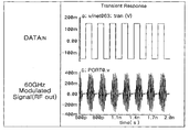
- FIG. 5 illustrates waveforms of 10 Gbps OOK input data and OOK modulated signal of the OOK modulator shown in FIG. 3.
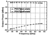
- FIG. 6A is a frequency-specific simulation result of output power characteristics in an on / off state of the OOK modulator shown in FIG. 3.
- FIG. 6B is a frequency-specific simulation result of on-off isolation (ratio of output power in on state and output power in off state) of the OOK modulator shown in FIG. 3.
- An OOK modulation device comprising: an oscillator for outputting a first frequency signal whose frequency varies according to an input voltage; A frequency multiple switching unit configured to drive on / off a second frequency signal obtained by multiplying the first frequency signal by driving according to on-off keying (OOK) input data; And a switching amplifier for amplifying and switching the second frequency signal according to the OOK input data and outputting a OOK modulated signal.
- OOK on-off keying
- FIG. 2 is a block diagram of an OOK modulation apparatus according to the present invention, which includes an oscillator 210, a frequency multiple switching unit 220, a digital data conversion unit 230, and a switching amplifier 240.
- the present invention modulates and outputs OOK input data through a carrier wave in which the frequency multiple switching unit 220 operates in an ON state during OOK modulation to multiply the frequency of the output signal of the oscillator 210, and outputs the modulated OOK input data. Since the switching amplification unit 240 and the frequency multiple switching unit 220 are not driven and there is almost no output power, the switching amplification unit 240 and the frequency multiple switching unit 220 are identified as "0" signals on binary codes of 1 or 0. Therefore, the on / off isolation characteristic and output power, which are the difference between the output power in the on state and the off state, are greatly improved.
- the oscillator 210 changes its output frequency when the input voltage Vtune is adjusted.
- the oscillator is a voltage controlled oscillator, for example, outputs a 30 GHz signal when an input voltage (Vtune) of 1 V is applied and outputs a 29 GHz signal when an input voltage (Vtune) of 0.7 V is applied.
- Oscillators generating low frequency carriers have many advantages over oscillators generating high frequency carriers.
- the oscillator outputs a low frequency signal
- the transconductance, inductance and Q value increase, and the oscillator's core can swing to a large output voltage, and the oscillator can be directly connected without a buffer. It has an output power characteristic.
- the present invention generates a low frequency signal in the oscillator, and generates a high frequency signal in a circuit of a frequency multiplying function with a switching function added to the low frequency signal, and in addition to the advantages of a low frequency generating oscillator, This further secures low power and on / off isolation characteristics.
- the frequency multiple switching unit 220 integrally multiplies the frequency of the first frequency signal V1 and switches according to an on / off level of the OOK input data DATA IN to output a second frequency signal V2. Since the frequency multiple switching unit 220 outputs a signal of 0 in the off state, power consumption may be reduced.
- the frequency multiplier switching unit 220 connects the oscillator 210 and the switching amplifier 240 to a frequency multiplier, but performs a switching operation according to the OOK input data as well as the frequency multiplication function. Referring to FIG. 3, the frequency multiplier switching unit 220 is connected to the switching amplifier 240 and outputs a frequency multiplication signal when the signal is turned on according to the on / off level of the OOK input data, but is 0 when the off state. Since the signal is output, a modulated signal including the information of the OOK input data is output.
- the digital data converter 230 converts the amplitude of the OOK input data DATA IN and outputs the amplitude to the switching amplifier 240.
- the digital data converter 230 may be implemented as a CML-CMOS conversion circuit 230 that converts a current mode logic (CML) level signal to a CMOS level.
- CML current mode logic
- a signal swinging at the CML level is used as an input / output interface of a signal operating at a high speed such as a clock signal.
- the CML level is the average level determined by the predetermined direct current level and is a signal that toggles with a predetermined amplitude swing.
- the CML-CMOS conversion circuit used in the present invention is a converter for converting a differential signal into a single signal.
- the OOK input data DATA IN is digital data, for example, a 10 Gbps digital data signal.
- the OOK input data DATA IN is a signal including information to be transmitted by the OOK modulator.
- the switching amplifier 240 amplifies the second frequency signal V2 according to an on / off level of the level conversion data in which the amplitude of the OOK input data DATA IN is increased to generate a OOK modulated signal RF OUT .
- Outputs The switching amplifier 240 performs a switching operation according to the information of the OOK input data DATA IN as well as an amplification function.
- the switching amplifier 240 amplifies and outputs the second frequency signal in an on state, and outputs a signal of almost zero in an off state.
- the conventional patent has a large power consumption as a 60 GHz oscillator, and a separate buffer circuit must be provided to connect the oscillator, whereas the present invention operates only an oscillator of 30 GHz in an off state compared to the conventional patent, and operates with a frequency multiple switching unit 220. Since there is almost no power consumption in the switching amplifier 240, there is an effect that can greatly reduce the power consumption.
- FIG. 3 is a circuit diagram of an OOK modulation apparatus according to the present invention shown in FIG.
- the oscillator 210 includes a first transistor M1 and a second transistor M2, a ninth inductor Lp1, a tenth inductor Lp2, a first variable capacitor Cp1, and a second gate and a drain which are cross-connected. It consists of the variable capacitor Cp2.
- the first transistor M1 and the second transistor M2 have their respective sources connected to ground and their gates and drains cross-connected.
- the ninth inductor Lp1 the first supply voltage VDD1 is supplied to one end and the other end thereof is connected to the drain of the first transistor M1.
- the tenth inductor Lp2 the first supply voltage VDD1 is supplied to one end and the other end thereof is connected to the drain of the second transistor M2.
- the input voltage Vtune is supplied to one end and the other end of the first variable capacitor Cp1 is connected to the other end of the ninth inductor Lp1.
- the second variable capacitor Cp2 the input voltage Vtune is supplied to one end and the other end thereof is connected to the other end of the tenth inductor Lp2.
- the transistors M1 to M6 may be implemented as CMOS transistors, but may be implemented as CMOS transistors having a 90 nm gate length, but are not limited thereto.
- the frequency multiplier switching unit 220 includes a first coupling capacitor C C 1, a second coupling capacitor C C 2, a first resistor Rb1, a second resistor Rb2, and a third transistor M3. ), A fourth transistor M4, a first inductor L1, and a second inductor L2.
- the first coupling capacitor C C 1 receives the first frequency signal V1 at one end.
- the second coupling capacitor C C 2 receives the phase inversion signal V1B of the first frequency signal V1.
- the first resistor Rb1 receives the gate voltage Vg at one end and is connected to the other end and the other end of the first coupling capacitor CC1.
- the gate voltage Vg is a DC voltage of a constant magnitude, for example, 0.4V.
- the second resistor Rb2 receives the gate voltage Vg at one end thereof and is connected to the other end and the other end of the second coupling capacitor C C 2.
- the third transistor M3 has a gate connected to the other end of the first coupling capacitor C C 1 and a ground connected to a source thereof.
- the other end of the second coupling capacitor C C 2 is connected to a gate of the fourth transistor M4, and a ground is connected to a source thereof.
- the first inductor L1 is connected between the drain of the third transistor M3 and the output terminal of the second frequency signal V2.
- the second inductor L2 is connected between the drain of the fourth transistor M4 and the output terminal of the second frequency signal V2.
- the switching amplifier 240 includes a second capacitor Cb1, a fifth inductor L5, a fourth inductor L4, a third coupling capacitor C C 3, a third inductor L3, and an eighth inductor (L8), a sixth transistor M6, a fourth coupling capacitor C C4 , and a seventh inductor L7.
- the second capacitor Cb1 is connected between the input terminal of the level conversion data DATA IN ′ and the ground.
- One end of the fifth inductor L5 is connected to an input terminal of the level conversion data DATA IN ′.
- the fourth inductor L4 is connected to the other end of the fifth inductor L5.
- the third coupling capacitor C 3 is connected to the other end of the fifth inductor L 5.
- An eighth inductor L8 is connected between the other end of the third coupling capacitor C C 3 and the output end of the second frequency signal V2.
- One end of the third inductor L3 is connected to the other end of the third coupling capacitor C C 3.
- the other end of the fourth inductor L4 is connected to a gate of the sixth transistor M6, and the other end of the third inductor L3 is connected to a source thereof.
- the first capacitor C1 is connected between the source and the ground of the sixth transistor M6.
- One end of the sixth inductor L6 is connected to the drain of the sixth transistor M6.
- the seventh inductor L7 receives the second supply voltage VDD2 at one end and is connected to the other end of the sixth inductor L6.
- the fourth coupling capacitor C C 4 is connected between the other end of the sixth inductor L6 and the output end of the switching amplifier 240.
- the first frequency signal V1 of 30 GHz is output from the oscillator 210 by LC resonance.
- the third transistor M3 and the fourth transistor M4 have a nonlinear characteristic and are respectively input to the first frequency signal V1 (30 GHz). Accordingly, the frequency is doubled and output to the output terminal of the frequency multiple switching unit 220 through the first inductor L1 and the second inductor L2, respectively. That is, when the second harmonics of the third transistor M3 and the fourth transistor M4 are matched, only the second harmonic can be output.
- the signal in which the first frequency signal V1 is doubled through the first inductor L1 is doubled and the phase inversion signal V1B of the first frequency signal V1 is doubled through the second inductor L2.
- the signals are added in the same phase so that the frequency multiple switching unit 220 outputs the second frequency signal V2 (60 GHz).
- the swing width of the OOK input data DATA IN is about 0.3 V
- the swing width of the output terminal is about 0.7 V or more to output the OOK modulated signal.
- 6A and 6B are graphs showing simulation results of output power and on / off isolation characteristics for each frequency of the OOK modulator shown in FIG. 3.
- the output of the OOK modulated signal in the on state is more than -4dBm and the output of the OOK modulated signal in the off state is less than -35dBm.
- the on / off isolation characteristic ratio of output power in the on state and output power in the off state
- the OOK modulator according to the present invention can be applied to a transmitter including an antenna for transmitting a modulated signal to the outside, and in particular, can be applied to a wireless personal area network (PAN) communication system in a millimeter wave band.
- PAN personal area network
- the OOK modulator according to the present invention improves the function of the conventional OOK modulator to significantly reduce power consumption and reduces power loss by using an oscillator that outputs a low frequency signal as compared with a conventional high frequency oscillator. Since the drain switch is not driven in the off state, further reduction in power consumption and on / off isolation characteristics are greatly improved.
- the present invention power consumption is greatly reduced, on / off isolation characteristics are improved by 15 dB or more, and data transmission characteristics are greatly improved, and thus, the present invention can be applied to a high-efficiency wireless transmission apparatus.
Landscapes
- Engineering & Computer Science (AREA)
- Computer Networks & Wireless Communication (AREA)
- Signal Processing (AREA)
- Power Engineering (AREA)
- Physics & Mathematics (AREA)
- Nonlinear Science (AREA)
- Spectroscopy & Molecular Physics (AREA)
- Amplifiers (AREA)
- Transmitters (AREA)
- Inductance-Capacitance Distribution Constants And Capacitance-Resistance Oscillators (AREA)
Abstract
본 발명에 따른 OOK 변조 장치는 입력전압에 따라 주파수가 가변되는 제1 주파수 신호를 출력하는 오실레이터; OOK 입력 데이터에 따라 구동하여 상기 제1 주파수 신호를 정수배한 제2 주파수 신호를 온/오프 스위칭하는 주파수 배수 스위칭부; 및 상기 OOK 입력 데이터에 따라 상기 제2 주파수 신호를 증폭 및 스위칭하여 OOK 변조 신호를 출력하는 스위칭 증폭부를 포함하는 것을 특징으로 한다.
Description
본 발명은 저전력 및 높은 온/오프 아이솔레이션 특성의 OOK(on-off keying) 변조 장치에 관한 것으로서, 더욱 상세하게는 상대적으로 낮은 주파수 신호를 출력하는 오실레이터와 스위칭 기능과 주파수 체배 기능을 동시에 갖는 주파수 배수 스위칭부에 의해 동일 주파수 대역의 변조를 수행하면서도 OOK 변조 동작 중 오프 상태에서 전력 소모를 크게 감소시킬 수 있고, 높은 온/오프 아이솔레이션 특성 및 고출력 파워 특성을 갖는 OOK 변조 장치에 관한 것이다.
이동 단말기를 이용한 응용 기술은 이동 단말기 내의 제한적 전력으로 인한 시스템의 저전력화가 무엇보다도 중요하다.
통신 시스템의 저전력화를 위하여 여러 방법이 제시되고 있으며, 이중 OOK 변조 방식을 이용한 자기-헤테로다인(self heterodyne) 구조는 도 1에 도시된 바와 같이, 시스템 구조의 간략화와 함께 PLL(phase locked loop)과 같은 국부 발진기의 고정 회로와 같은 전력 소모가 큰 부품을 포함시킬 필요가 없기 때문에 시스템 전체의 전력 소모를 획기적으로 감소시킬 수 있어 저전력을 요하는 이동 단말기의 탑재에 적합하다.
도 1은 일반적인 이동 단말기에 탑재 가능한 밀리미터파 대역의 Gbps 고속 OOK 신호 변조 장치가 적용된 송신기를 도시한 도면으로서, 입력단을 통해 Gbps OOK 데이터 신호를 입력받아 이를 변조하여 출력하는 변조기(100) 및 안테나(ANT)를 통해 변조기(100)에서 출력되는 신호를 송신한다.
이러한 자기-히테로다인 구조의 OOK 변조 방법이 적용된 송신 장치는 수신 장치에서 OOK 신호를 복조하도록 OOK 데이터 신호와 함께 로컬 캐리어(local carrier) 신호를 동시에 송신하며, 송신 장치의 변조기(100)는 일반적인 전력 증폭기를 대신하여 OOK 데이터 신호가 "1"일 경우 전류가 흘러 출력 신호를 안테나를 통해 전송하고, OOK 데이터 신호가 "0"일 경우 전류가 흐르지 않게 되며 출력으로 아무런 신호가 발생하지 않게 된다.
OOK 변조 장치를 설계할 때 가장 중요한 항목은 OOK 입력 데이터의 온 상태(on state)와 오프 상태(off state)에 따라 변조 장치의 온/오프 아이솔레이션 특성, 온 상태에서 전달되는 신호의 이득, 전력소모 및 처리 가능한 데이터 속도이다.
종래의 OOK 변조 장치는 주파수 특성상 회로의 낮은 신호 이득과 신호 누출 현상 등의 단점을 가지고 있으며, 저가격과 저전력을 위해 사용되는 시모스(complementary metal oxide semiconductor: CMOS) 공정을 이용하여 변조 장치를 설계할 경우 단점은 더욱 더 커지게 된다.
이런 이유로, 신호 손실이 크고 신호 누출도 큰 밀리미터 대역에서 높은 온/오프 아이솔레이션 특성과 Gbps 이상의 고속 데이터 처리가 가능한 저전력 구조를 갖는 OOK 변조 장치의 개발이 절실히 요구되고 있다.
한국공개특허 제10-2012-0038275호(2012년 04월 23일 공개)에 기술된 OOK 변조 장치는 다수의 증폭기를 이용하여 하나의 증폭기의 증폭된 신호에 의해 다른 증폭기가 공통 소스 증폭기로 동작함에 따라 고파워 레벨의 OOK 변조 신호를 출력하는 기술이다. 상기 OOK 변조 장치는 반송파를 발생시키는 오실레이터를 추가로 구비하고 있다. OOK 변조 장치에서 요구되는 고속 데이터 처리를 위한 오실레이터에서 발생시키는 신호가 고주파 반송파이므로 오실레이터의 소모전력이 매우 크고, 변조 장치와 연결 구성하기 위한 버퍼 등의 추가 회로를 구비해야 하는 문제점이 있다.
상기의 해결하려는 과제를 위한 본 발명에 따른 OOK 변조 장치는 입력전압에 따라 주파수가 가변되는 제1 주파수 신호를 출력하는 오실레이터; OOK 입력 데이터에 따라 구동하여 상기 제1 주파수 신호를 정수배한 제2 주파수 신호를 온/오프 스위칭하는 주파수 배수 스위칭부; 및 상기 OOK 입력 데이터에 따라 상기 제2 주파수 신호를 증폭 및 스위칭하여 OOK 변조 신호를 출력하는 스위칭 증폭부를 포함하는 것을 특징으로 한다.
본 발명에 따른 다른 실시예로서, OOK 변조방법은 오실레이터는 데이터 변조시에 항상 동작하고, 주파수 배수 스위칭부와 상기 스위칭 증폭부는 입력 데이터의 온(on) 상태와 오프(off) 상태에 따라서 동시에 동작하는 것을 특징으로 한다.
본 발명의 바람직한 실시예로서, 상기 입력 데이터가 온 상태일 경우, 상기 주파수 배수 스위칭부의 트랜지터와 상기 스위칭 증폭부의 트랜지스터가 동시에 온 상태로 동작하고, 상기 입력 데이터가 오프 상태일 경우, 상기 주파수 배수 스위칭부의 트랜지터와 상기 스위칭 증폭부의 트랜지스터가 동시에 오프 상태로 동작하여 전력소모를 줄이는 것을 특징으로 한다.
상기의 해결하려는 과제를 위한 본 발명에 따른 OOK 변조 장치는 입력전압에 따라 주파수가 가변되는 제1 주파수 신호를 출력하는 오실레이터; OOK 입력 데이터에 따라 구동하여 상기 제1 주파수 신호를 정수배한 제2 주파수 신호를 온/오프 스위칭하는 주파수 배수 스위칭부; 및 상기 OOK 입력 데이터에 따라 상기 제2 주파수 신호를 증폭 및 스위칭하여 OOK 변조 신호를 출력하는 스위칭 증폭부를 포함하는 것을 특징으로 한다.
본 발명에 따른 다른 실시예로서, OOK 변조방법은 오실레이터는 데이터 변조시에 항상 동작하고, 주파수 배수 스위칭부와 상기 스위칭 증폭부는 입력 데이터의 온(on) 상태와 오프(off) 상태에 따라서 동시에 동작하는 것을 특징으로 한다.
본 발명의 바람직한 실시예로서, 상기 입력 데이터가 온 상태일 경우, 상기 주파수 배수 스위칭부의 트랜지터와 상기 스위칭 증폭부의 트랜지스터가 동시에 온 상태로 동작하고, 상기 입력 데이터가 오프 상태일 경우, 상기 주파수 배수 스위칭부의 트랜지터와 상기 스위칭 증폭부의 트랜지스터가 동시에 오프 상태로 동작하여 전력소모를 줄이는 것을 특징으로 한다.
본 발명은 소모전력이 크게 감소되고, 온/오프 아이솔레이션(isolation) 특성이 15dB 이상 개선되고, 데이터 전송 특성이 크게 개선된다.
본 발명은 별도의 앰프 및 업 컨버터 믹서(up converter mixer)를 사용하지 않고도 고출력 신호를 생성하므로, 별도의 회로를 구비하지 않아도 동등한 출력 특성을 확보할 수 있으므로 소형화, 저전력 및 저단가 효과가 있다.
도 1은 종래 기술에 따른 이동 단말기에 탑재 가능한 밀리미터파 대역의 Gbps 고속 OOK 신호 변조 장치가 적용된 송신기다.
도 2는 본 발명에 따른 OOK 변조 장치의 블록도이다.
도 3은 도 2에 도시된 OOK 변조 장치의 상세 회로도이다.
도 4는 도 3에 도시된 OOK 변조 장치의 오프 상태에서의 등가 회로 및 신호 파형을 도시한 것이다.
도 5는 도 3에 도시된 OOK 변조 장치의 10Gbps OOK 입력 데이터와 OOK 변조 신호의 파형을 도시한 것이다.
도 6a는 도 3에 도시된 OOK 변조 장치의 온/오프 상태에서의 출력 파워 특성의 주파수별 시뮬레이션 결과이다.
도 6b는 도 3에 도시된 OOK 변조 장치의 온-오프 아이솔레이션(온 상태의 출력 파워와 오프 상태의 출력 파워의 비) 특성의 주파수별 시뮬레이션 결과이다.
OOK 변조 장치에 있어서, 입력전압에 따라 주파수가 가변되는 제1 주파수 신호를 출력하는 오실레이터; OOK(on-off keying) 입력 데이터에 따라 구동하여 상기 제1 주파수 신호를 정수배한 제2 주파수 신호를 온/오프 스위칭하는 주파수 배수 스위칭부; 및 상기 OOK 입력 데이터에 따라 상기 제2 주파수 신호를 증폭 및 스위칭하여 OOK 변조 신호를 출력하는 스위칭 증폭부를 포함하는 것을 특징으로 한다.
이하 본 발명의 실시를 위한 구체적인 실시예를 도면을 참고하여 설명한다.
도 2는 본 발명에 따른 OOK 변조 장치의 블록도로서, 오실레이터(210), 주파수 배수 스위칭부(220), 디지털 데이터 변환부(230) 및 스위칭 증폭부(240)를 포함한다.
본 발명은 OOK 변조시 온 상태(ON state)에서 주파수 배수 스위칭부(220)가 동작하여 오실레이터(210)의 출력 신호의 주파수를 배수화한 반송파를 통해 OOK 입력 데이터를 변조하여 출력하며, 오프 상태에서 스위칭 증폭부(240)와 주파수 배수 스위칭부(220)가 구동되지 않아 출력 전력이 거의 없으므로 1 또는 0의 이진 코드상 "0" 신호로 식별된다. 따라서, 온 상태와 오프상태에서의 출력 파워 차이인 온/오프 아이솔레이션 특성 및 출력 파워를 크게 개선하였다.
상기 오실레이터(210)는 입력전압(Vtune)을 조절하면 출력 주파수가 변화된다. 상기 오실레이터는 전압제어 오실레이터로서, 예를 들면 1V의 입력전압(Vtune)이 인가되면 30GHz 신호를 출력하고, 0.7V의 입력전압(Vtune)이 인가되면 29GHz 신호를 출력한다.
고주파 반송파를 발생시키는 오실레이터보다 저주파 반송파를 발생시키는 오실레이터는 많은 장점을 갖는다. 오실레이터가 저주파 신호를 출력할수록 트랜스 컨덕턴스와 인덕턴스 및 Q값이 높아지고 오실레이터의 코어(core)에서 큰 출력 전압으로 스윙(swing)할 수 있으며, 오실레이터에 버퍼가 없이도 바로 연결 구성할 수 있으므로 적은 전력으로 큰 출력 파워 특성을 갖게 된다. 본 발명은 오실레이터에서 저주파 신호를 발생시키고, 저주파 신호를 스위칭 기능이 추가된 주파수 체배 기능의 회로로 고주파 신호를 발생시킴으로써, 저주파 발생 오실레이터의 장점과 아울러, 오프 상태에서 구동하지 않는 주파수 배수 스위칭부에 의해 저전력 및 온/오프 아이솔레이션 특성을 추가로 확보할 수 있다.
상기 주파수 배수 스위칭부(220)는 상기 제1 주파수 신호(V1)의 주파수를 정수배하고 상기 OOK 입력 데이터(DATAIN)의 온/오프 레벨에 따라 스위칭되어 제2 주파수 신호(V2)를 출력한다. 주파수 배수 스위칭부(220)는 오프 상태에서 0인 신호를 출력하므로 전력 소모를 감소시킬 수 있다. 상기 주파수 배수 스위칭부(220)는 주파수 체배기로 오실레이터(210)와 스위칭 증폭부(240)를 연결하지만 주파수 체배 기능뿐만 아니라 OOK 입력 데이터에 따른 스위칭 동작을 수행한다. 도 3을 참조하면, 상기 주파수 배수 스위칭부(220)는 상기 스위칭 증폭부(240)와의 연결되어 OOK 입력 데이터의 온/오프 레벨에 따라 온 상태이면 주파수 체배 신호를 출력하나, 오프 상태이면 0인 신호를 출력하므로 OOK 입력 데이터의 정보를 포함하는 변조 신호를 출력한다.
상기 디지털 데이터 변환부(230)는 OOK 입력 데이터(DATAIN)를 진폭을 변환하여 상기 스위칭 증폭부(240)로 출력한다. 상기 디지털 데이터 변환부(230)는 CML(current mode logic) 레벨의 신호를 CMOS 레벨로 변환하는 CML-CMOS 변환 회로(230)로 구현할 수 있다. 일반적으로 클록(clock) 신호 등과 같이 고속으로 동작하는 신호의 입출력 인터페이스는 CML 레벨에서 스윙하는 신호가 사용된다. CML 레벨은 예정된 직류 레벨에 의해 결정된 평균레벨로서 예정된 진폭 스윙을 갖고 토글링하는 신호이다. 이러한 신호는 상대적으로 작은 스윙폭으로 인하여 전압레벨에 따라 데이터의 논리를 판단해야 하는 장치에서는 사용할 수 없기 때문에 CMOS 레벨로 스윙하는 신호를 사용해야 한다. CMOS 레벨로 스윙하는 신호는 전원전압과 접지전압까지 풀스윙(full swing)하기 때문에 상대적으로 스윙폭이 크다. 본 발명에서 사용하는 CML-CMOS 변환회로는 차동신호를 단일신호로 변환하는 변환기이다.
상기 OOK 입력 데이터(DATAIN)는 디지털 데이터로서 예를 들면, 10Gbps 디지털 데이터 신호이다. 상기 OOK 입력 데이터(DATAIN)는 OOK 변조 장치에서 송신하려고 하는 정보를 포함하는 신호이다.
상기 스위칭 증폭부(240)는 상기 OOK 입력 데이터(DATAIN)의 진폭이 증가된 상기 레벨 변환 데이터의 온/오프 레벨에 따라 상기 제2 주파수 신호(V2)를 증폭하여 OOK 변조 신호(RFOUT)를 출력한다. 상기 스위칭 증폭부(240)는 단순히 증폭 기능뿐만 아니라 OOK 입력 데이터(DATAIN)의 정보에 따라 스위칭 동작을 한다. 상기 스위칭 증폭부(240)는 온 상태에서 상기 제2 주파수 신호를 증폭하여 출력하고, 오프 상태에서 거의 0인 신호를 출력한다.
종래 특허는 60GHz 오실레이터로서 전력 소모가 크며, 오실레이터를 연결하는데 별도의 버퍼 회로를 구비해야 하는 반면, 본 발명은 종래 특허에 비해 오프 상태에서는 30GHz의 오실레이터만 동작하고, 주파수 배수 스위칭부(220)와 상기 스위칭 증폭부(240)에서의 전력 소모가 거의 없게 되므로 소모 전력을 크게 감소시킬 수 있는 효과가 있다.
도 3은 도 2에 도시된 본 발명에 따른 OOK 변조 장치의 회로도이다.
상기 오실레이터(210)는 게이트와 드레인이 크로스 연결된 제1 트랜지스터(M1)와 제2 트랜지스터(M2), 제9 인덕터(Lp1), 제10 인덕터(Lp2), 제1 가변 캐패시터(Cp1), 제2 가변 캐패시터(Cp2)로 구성된다.
제1 트랜지스터(M1)와 제2 트랜지스터(M2)는 각각의 소스가 그라운드에 연결되고 게이트와 드레인이 크로스 연결된다. 제9 인덕터(Lp1)는 상기 제1 공급전압(VDD1)이 일단에 공급되고 상기 제1 트랜지스터(M1)의 드레인에 타단이 연결된다. 제10 인덕터(Lp2)는 상기 제1 공급전압(VDD1)이 일단에 공급되고 상기 제2 트랜지스터(M2)의 드레인에 타단이 연결된다. 제1 가변 캐패시터(Cp1)는 상기 입력전압(Vtune)이 일단에 공급되고 상기 제9 인덕터(Lp1)의 타단에 타단이 연결된다. 제2 가변 캐패시터(Cp2)는 상기 입력전압(Vtune)이 일단에 공급되고 상기 제10 인덕터(Lp2)의 타단에 타단이 연결된다. 상기 트랜지스터(M1~M6)는 시모스 트랜지스터로 구현할 수 있으며, 바람직하게는 90nm 게이트 길이를 갖는 시모스 트랜지스터로 구현할 수 있지만, 이에 제한되지 않는다.
상기 주파수 배수 스위칭부(220)는 제1 커플링 캐패시터(CC1), 제2 커플링 캐패시터(CC2), 제1 레지스터(Rb1), 제2 레지스터(Rb2), 제3 트랜지스터(M3), 제4 트랜지스터(M4), 제1 인덕터(L1) 및 제2 인덕터(L2)로 연결 구성한다.
제1 커플링 캐패시터(CC1)는 상기 제1 주파수 신호(V1)를 일단에 입력받는다.제2 커플링 캐패시터(CC2)는 상기 제1 주파수 신호(V1)의 위상 반전 신호(V1B)를 일단에 입력받는다. 제1 레지스터(Rb1)는 상기 게이트 전압(Vg)을 일단에 입력받고 상기 제1 커플링 캐패시터(CC1)의 타단과 타단이 연결된다. 게이트 전압(Vg)은 일정한 크기의 DC 전압이고, 예를 들면, 0.4V이다. 제2 레지스터(Rb2)는 상기 게이트 전압(Vg)을 일단에 입력받고 상기 제2 커플링 캐패시터(CC2)의 타단과 타단이 연결된다. 제3 트랜지스터(M3)는 게이트에 상기 제1 커플링 캐패시터(CC1)의 타단이 연결되고 소스에 그라운드가 연결된다. 제4 트랜지스터(M4)는 게이트에 상기 제2 커플링 캐패시터(CC2)의 타단이 연결되고 소스에 그라운드가 연결된다. 제1 인덕터(L1)는 상기 제3 트랜지스터(M3)의 드레인과 상기 제2 주파수 신호(V2)의 출력단 사이에 연결된다. 제2 인덕터(L2)는 상기 제4 트랜지스터(M4)의 드레인과 상기 제2 주파수 신호(V2)의 출력단 사이에 연결된다.
상기 스위칭 증폭부(240)는 제2 캐패시터(Cb1), 제5 인턱터(L5), 제4 인덕터(L4), 제3 커플링 캐패시터(CC3), 제3 인턱터(L3), 제8 인덕터(L8), 제6 트랜지스터(M6), 제4 커플링 캐패시터(CC4) 및 제7 인덕터(L7)로 구성된다.
제2 캐패시터(Cb1)는 상기 레벨 변환 데이터(DATAIN')의 입력단과 그라운드 사이에 연결된다. 제5 인덕터(L5)는 상기 레벨 변환 데이터(DATAIN')의 입력단에 일단이 연결된다. 제4 인덕터(L4)는 상기 제5 인덕터(L5)의 타단에 연결된다. 제3 커플링 캐패시터(CC3)는 상기 제5 인덕터(L5)의 타단에 연결된다. 제8 인덕터(L8)는 상기 제3 커플링 캐패시터(CC3)의 타단과 상기 제2 주파수 신호(V2)의 출력단 사이에 연결된다. 제3 인덕터(L3)은 상기 제3 커플링 캐패시터(CC3)의 타단에 일단이 연결된다. 제6 트랜지스터(M6)는 게이트에 상기 제4 인덕터(L4)의 타단이 연결되고, 소스에 상기 제3 인덕터(L3)의 타단이 연결된다. 제1 캐패시터(C1)는 상기 제6 트랜지스터(M6)의 소스와 그라운드 사이에 연결된다. 제6 인덕터(L6)는 상기 제6 트랜지스터(M6)의 드레인에 일단이 연결된다. 제7 인덕터(L7)는 상기 제2 공급 전압(VDD2)을 일단에 입력받고 상기 제6 인덕터(L6)의 타단에 타단이 연결된다. 제4 커플링 캐패시터(CC4)는 상기 제6 인덕터(L6)의 타단과 상기 스위칭 증폭부(240)의 출력단 사이에 연결된다.
본 발명에 따른 OOK 변조 장치의 동작을 도 3과 도 4를 참조하여 설명하면 다음과 같다.
입력전압(Vtune)에 1V를 인가하면, LC 공진에 의해 상기 오실레이터(210)에서 30GHz의 제1 주파수 신호(V1)가 출력된다.
OOK 입력 데이터(DATAIN)가 “1”일 경우, 즉 온(ON) 상태에서의 동작은 도 3을 참조하면 다음과 같다.
상기 OOK 입력 데이터(DATAIN)가 “1”일 때, 상기 제3 트랜지스터(M3)와 상기 제4 트랜지스터(M4)는 비선형 특성으로 각각의 게이트에 입력되는 제1 주파수 신호(V1)(30GHz)에 따라 각각 제1 인덕터(L1)와 제2 인덕터(L2)를 통해 상기 주파수 배수 스위칭부(220)의 출력단으로 주파수를 2배시켜 출력한다. 즉, 제3 트랜지스터(M3)와 제4 트랜지스터(M4)의 2차 고조파에 정합을 하면 2차 고조파만 출력시킬 수 있다. 상기 제1 인덕터(L1)를 통해서는 제1 주파수 신호(V1)를 2배한 신호가, 상기 제2 인덕터(L2)를 통해서는 제1 주파수 신호(V1)의 위상 반전 신호(V1B)를 2배한 신호가 같은 위상으로 더해져서 상기 주파수 배수 스위칭부(220)에서 제2 주파수 신호(V2)(60GHz)를 출력한다.
상기 OOK 입력 데이터(DATAIN)가 “1”인 경우, 제6 트랜지스터(M6)가 동작하여 상기 스위칭 증폭부(240)의 출력단에서 상기 레벨 변환 데이터(DATAIN')가 “1”인 경우 제2 주파수 신호(V2)를 증폭한 OOK 변조 신호(RFOUT)가 출력된다.
OOK 입력 데이터(DATAIN)가 “0”일 경우, 오프(OFF) 상태에서의 동작은 도 4를 참조하면 다음과 같다.
상기 OOK 입력 데이터(DATAIN)가 “0”일 때, 상기 스위칭 증폭부의 출력단에서 신호가 출력되지 않을 뿐만 아니라 상기 주파수 배수 스위칭부의 출력단과의 연결 노드에서도 신호가 출력되지 않아 오프상태가 된다. 따라서 상기 주파수 배수 스위칭부의 출력단의 전압이 0이므로 상기 제3 트랜지스터(M3)와 상기 제4 트랜지스터(M4)는 서브쓰레쉬홀드(subthreshold) 영역에서 동작하므로 오프상태의 캐패시터(Coff)와 같고, 드레인과 소스에는 오프 저항(Roff)과 같다. 상기 오프 저항(Roff)값은 매우 작으므로, 상기 제1 커플링 캐패시터(CC1)로부터 이동된 제1 주파수 신호(V1)(30GHz)는 거의 대부분이 오프 저항(Roff: 제3 트랜지스터(M3)의 오프 상태에서의 등가저항)과 제4 트랜지스터(M4)의 게이트-소스로 흘러들어가고, 제1 인덕터(L1)로 흘러가는 신호는 미약하여 상기 주파수 배수 스위칭부(220)는 0에 가까운 신호를 출력한다. 또한, 오프 상태에서 제6 트랜지스터(M6)도 오프 캐패시터(Coff)와 같으므로 상기 스위칭 증폭부(240)의 출력단에서는 0에 가까운 신호를 출력한다.
그 결과, 상기 OOK 입력 데이터(DATAIN)의 온/오프에 따라 온 상태에서 제1 주파수 신호의 주파수를 2배시키고 증폭시킨 신호가 출력되고, 오프 상태에서 0에 가까운 신호가 발생한다. 오프 상태에서 오실레이터(210)를 제외하고는 각각의 트랜지스터, 저항, 인덕터 및 캐패시터에서 전력 소모가 없으며, 온 상태에서 앰프없이도 저전력으로 큰 출력 파워의 OOK 변조 신호를 출력한다.
도 5를 참조하면, OOK 입력 데이터(DATAIN)의 스윙폭이 약 0.3 V일 때, 출력단의 스윙폭은 약 0.7 V이상으로 OOK 변조 신호를 출력함을 보여준다.
도 6a 및 도 6b는 도 3에 도시된 OOK 변조 장치의 주파수별 출력 파워와 온/오프 아이솔레이션 특성을 시뮬레이션한 결과 그래프이다. 57.5~64.5GHz 대역에서 온상태의 OOK 변조 신호의 출력은 -4dBm 이상이며, 오프 상태의 OOK 변조 신호의 출력은 -35dBm 이하이다. 또한, 온/오프 아이솔레이션 특성(온 상태의 출력 파워와 오프 상태의 출력파워의 비)은 주파수 증가시 아이솔레이션 특성이 저하됨에도 57.5~ 64.5GHz 대역에서 -46~-36dB로 온/오프 아이솔레이션 특성이 종래 특허에 비해 약 15dB 이상 개선되었음을 보여준다.
본 발명에 따른 OOK 변조 장치는 변조 신호를 외부로 송신하는 안테나를 포함하여 송신기에 응용할 수 있으며, 특히, 밀리미터파 대역의 무선 PAN(personal area network) 통신 시스템에도 응용할 수 있다.
본 발명에 따른 OOK 변조 장치는 종래 특허의 OOK 변조 장치의 기능을 개선하여 소모 전력을 크게 감소시킬 뿐 아니라 기존의 고주파 오실레이터에 비해 저주파 신호를 출력하는 오실레이터를 사용함에 따라 전력 손실을 감소시키고, 주파수 배수 스위칭부가 오프 상태에서는 구동하지 않기 때문에 추가의 전력 소모 감소 및 온/오프 아이솔레이션 특성이 크게 개선되는 효과가 나타난다.
이상에서는 실시예를 참조하여 설명하였지만, 해당 기술 분야의 숙련된 당업자는 하기의 특허 청구의 범위에 기재된 본 발명의 사상 및 영역으로부터 벗어나지 않는 범위 내에서 본 발명을 다양하게 수정 및 변경시킬 수 있음을 이해할 수 있을 것이다.
본 발명은 소모전력이 크게 감소되고, 온/오프 아이솔레이션(isolation) 특성이 15dB 이상 개선되고, 데이터 전송 특성이 크게 개선하여 고효율의 무선 전송장치에 적용할 수 있다.
또한 별도의 앰프 및 업 컨버터 믹서(up converter mixer)를 사용하지 않고도 고출력 신호를 생성하므로, 별도의 회로를 구비하지 않아도 동등한 출력 특성을 확보할 수 있으므로 소형화, 저전력 및 저단가로 구현하여 사용할 수 있으므로, 산업상 이용가능성이 있다.
Claims (12)
- 입력전압에 따라 주파수가 가변되어 제1 주파수 신호를 출력하는 오실레이터;OOK(on-off keying) 입력 데이터에 따라 구동하여 상기 제1 주파수 신호를 정수배한 제2 주파수 신호를 온/오프 스위칭하는 주파수 배수 스위칭부; 및상기 OOK 입력 데이터에 따라 상기 제2 주파수 신호를 증폭 및 스위칭하여 OOK 변조 신호를 출력하는 스위칭 증폭부를 포함하는 것을 특징으로 하는 OOK 변조 장치.
- 제1 항에 있어서,상기 OOK 입력 데이터의 진폭을 변환시켜 상기 스위칭 증폭부에 출력하는 디지털 데이터 변환부를 더 포함하는 것을 특징으로 하는 OOK 변조 장치.
- 제2 항에 있어서,상기 디지털 데이터 변환부는,CML(current mode logic) 레벨의 상기 OOK 입력 데이터를 CMOS 레벨로 변환하는 CML-CMOS 변환기인 것을 특징으로 하는 OOK 변조 장치.
- 제1 항에 있어서,상기 오실레이터는 전압제어 오실레이터인 것을 특징으로 하는 OOK 변조 장치.
- 제1 항에 있어서,상기 주파수 배수 스위칭부는,상기 제1 주파수 신호를 일단에 입력받는 제1 커플링 캐패시터;상기 제1 주파수 신호의 위상 반전 신호를 일단에 입력받는 제2 커플링 캐패시터;게이트에 상기 제1 커플링 캐패시터의 타단이 연결되고 소스에 그라운드가 연결된 제3 트랜지스터; 및게이트에 상기 제2 커플링 캐패시터의 타단이 연결되고 소스에 그라운드가 연결된 제4 트랜지스터를 포함하는 것을 특징으로 하는 OOK 변조 장치.
- 제5 항에 있어서,상기 주파수 배수 스위칭부는,상기 게이트 전압을 일단에 입력받고 상기 제1 커플링 캐패시터의 타단과 타단이 연결된 제1 레지스터; 및상기 게이트 전압을 일단에 입력받고 상기 제2 커플링 캐패시터의 타단과 타단이 연결된 제2 레지스터를 더 포함하는 것을 특징으로 하는 OOK 변조 장치.
- 제6 항에 있어서,상기 주파수 배수 스위칭부는,상기 제3 트랜지스터의 드레인과 상기 제2 주파수 신호의 출력단 사이에 연결된 제1 인덕터; 및상기 제4 트랜지스터의 드레인과 상기 제2 주파수 신호의 출력단 사이에 연결된 제2 인덕터를 더 포함하는 것을 특징으로 하는 OOK 변조 장치.
- 제1 항에 있어서,상기 스위칭 증폭부는,레벨 변환 데이터의 입력단과 그라운드 사이에 연결된 제2 캐패시터;상기 레벨 변환 데이터의 입력단에 일단이 연결된 제5 인덕터;상기 제5 인덕터의 타단에 연결된 제4 인덕터;상기 제5 인덕터의 타단에 연결된 제3 커플링 캐패시터;상기 제3 커플링 캐패시터의 타단과 상기 제2 주파수 신호의 출력단 사이에 연결된 제8 인덕터;상기 제3 커플링 캐패시터의 타단에 일단이 연결된 제3 인덕터;게이트에 상기 제4 인덕터의 타단이 연결되고, 소스에 상기 제3 인덕터의 타단이 연결된 제6 트랜지스터;상기 제6 트랜지스터의 소스와 그라운드 사이에 연결된 제1 캐패시터;상기 제6 트랜지스터의 드레인에 일단이 연결된 제6 인덕터;제2 공급 전압을 일단에 입력받고 상기 제6 인덕터의 타단에 타단이 연결된 제7 인덕터; 및상기 제6 인덕터의 타단과 상기 스위칭 증폭부의 출력 단 사이에 연결된 제4 커플링 캐패시터를 포함하는 것을 특징으로 하는 OOK 변조 장치.
- 제1 항에 있어서,상기 오실레이터는,각각의 소스가 그라운드에 연결되고 상호 게이트와 드레인이 크로스 연결된 제1 트랜지스터와 제2 트랜지스터;제1 공급전압이 일단에 공급되고 상기 제1 트랜지스터의 드레인에 타단이 연결된 제9 인덕터;상기 제1 공급전압이 일단에 공급되고 상기 제2 트랜지스터의 드레인에 타단이 연결된 제10 인덕터;상기 입력전압이 일단에 공급되고 상기 제9 인덕터의 타단에 타단이 연결된 제1 가변 캐패시터; 및상기 입력전압이 일단에 공급되고 상기 제10 인덕터의 타단에 타단이 연결된 제2 가변 캐패시터를 포함하는 것을 특징으로 하는 OOK 변조 장치.
- 입력전압에 따라 주파수가 가변되는 제1 주파수 신호를 출력하는 오실레이터, OOK(on-off keying) 입력 데이터에 따라 구동하여 상기 제1 주파수 신호를 정수배한 제2 주파수 신호를 온/오프 스위칭하는 주파수 배수 스위칭부 및 상기 OOK 입력 데이터에 따라 상기 제2 주파수 신호를 증폭 및 스위칭하여 OOK 변조 신호를 출력하는 스위칭 증폭부를 포함하는 OOK 변조 장치를 사용하여 변조하는 방법에 있어서,상기 오실레이터는 데이터 변조시에 항상 동작하고,상기 주파수 배수 스위칭부와 상기 스위칭 증폭부는 상기 입력 데이터의 온(on) 상태와 오프(off) 상태에 따라서 동시에 동작하는 것을 특징으로 하는 OOK 변조방법.
- 제11항에 있어서,상기 입력 데이터가 온 상태일 경우, 상기 주파수 배수 스위칭부의 트랜지터와 상기 스위칭 증폭부의 트랜지스터가 동시에 온 상태로 동작하는 것을 특징으로 하는 OOK 변조방법.
- 제11항에 있어서,상기 입력 데이터가 오프 상태일 경우, 상기 주파수 배수 스위칭부의 트랜지터와 상기 스위칭 증폭부의 트랜지스터가 동시에 오프 상태로 동작하는 것을 특징으로 하는 OOK 변조방법.
Priority Applications (1)
| Application Number | Priority Date | Filing Date | Title |
|---|---|---|---|
| US14/438,174 US9319256B2 (en) | 2012-11-01 | 2013-09-06 | OOK modulation device and wireless transmitting device including the same |
Applications Claiming Priority (2)
| Application Number | Priority Date | Filing Date | Title |
|---|---|---|---|
| KR10-2012-0123008 | 2012-11-01 | ||
| KR1020120123008A KR101392323B1 (ko) | 2012-11-01 | 2012-11-01 | Ook 변조 장치 및 이를 포함하는 무선 통신 송신 장치 |
Publications (1)
| Publication Number | Publication Date |
|---|---|
| WO2014069782A1 true WO2014069782A1 (ko) | 2014-05-08 |
Family
ID=50627639
Family Applications (1)
| Application Number | Title | Priority Date | Filing Date |
|---|---|---|---|
| PCT/KR2013/008065 Ceased WO2014069782A1 (ko) | 2012-11-01 | 2013-09-06 | Ook 변조 장치 및 이를 포함하는 무선 통신 송신 장치 |
Country Status (3)
| Country | Link |
|---|---|
| US (1) | US9319256B2 (ko) |
| KR (1) | KR101392323B1 (ko) |
| WO (1) | WO2014069782A1 (ko) |
Cited By (1)
| Publication number | Priority date | Publication date | Assignee | Title |
|---|---|---|---|---|
| WO2015191612A1 (en) * | 2014-06-09 | 2015-12-17 | The Regents Of The University Of California | Wireless data and power transfer over an inductive telemetry link |
Families Citing this family (11)
| Publication number | Priority date | Publication date | Assignee | Title |
|---|---|---|---|---|
| KR20150044538A (ko) * | 2013-10-17 | 2015-04-27 | 한국전자통신연구원 | Ook 변조를 위한 인터페이스 장치 및 이를 이용한 송신기 |
| US10270630B2 (en) * | 2014-09-15 | 2019-04-23 | Analog Devices, Inc. | Demodulation of on-off-key modulated signals in signal isolator systems |
| US10536309B2 (en) | 2014-09-15 | 2020-01-14 | Analog Devices, Inc. | Demodulation of on-off-key modulated signals in signal isolator systems |
| EP3203579B1 (en) | 2014-10-01 | 2019-11-20 | KMW Inc. | Portable antenna control device and antenna control system |
| US9998301B2 (en) | 2014-11-03 | 2018-06-12 | Analog Devices, Inc. | Signal isolator system with protection for common mode transients |
| US10193718B2 (en) | 2017-01-16 | 2019-01-29 | Electronics And Telecommunications Research Institute | Method for data modulation in wireless communication system and apparatus for the same |
| KR102387572B1 (ko) | 2017-04-20 | 2022-04-18 | 삼성전자주식회사 | 무선 통신 장치 및 방법 |
| KR102112855B1 (ko) * | 2018-01-08 | 2020-05-19 | 성균관대학교산학협력단 | 무선 통신 시스템에서 온-오프 키잉 방식을 이용하여 신호를 전송하기 위한 방법 및 장치 |
| US10848100B2 (en) * | 2018-09-17 | 2020-11-24 | Qualcomm Incorporated | System and method for reducing current noise in a VCO and buffer |
| US11863360B2 (en) * | 2022-01-25 | 2024-01-02 | Texas Instruments Incorporated | Methods and apparatus to reduce variations for on-off keying transmissions |
| EP4508810A4 (en) * | 2022-04-13 | 2026-05-20 | Nia Therapeutics Inc | TWO-WAY WIRELESS DATA AND POWER TRANSFER OVER INDUCTIVE LINK |
Citations (2)
| Publication number | Priority date | Publication date | Assignee | Title |
|---|---|---|---|---|
| WO2001028121A2 (en) * | 1999-10-15 | 2001-04-19 | Rf Waves Ltd. | Spread-spectrum modem with saw resonator and pulse shaping |
| KR20120092634A (ko) * | 2009-11-20 | 2012-08-21 | 주식회사 케이엠더블유 | 온오프 변조 방식을 이용한 신호 송수신 장치 |
Family Cites Families (2)
| Publication number | Priority date | Publication date | Assignee | Title |
|---|---|---|---|---|
| US7436263B2 (en) * | 2004-12-15 | 2008-10-14 | Texas Instruments Incorporated | Apparatus and method for presenting a modulated output signal at an output locus |
| JP5500679B2 (ja) * | 2010-03-19 | 2014-05-21 | シリコンライブラリ株式会社 | 無線伝送システム並びにそれに用いられる無線送信機、無線受信機、無線送信方法、無線受信方法、及び無線通信方法 |
-
2012
- 2012-11-01 KR KR1020120123008A patent/KR101392323B1/ko active Active
-
2013
- 2013-09-06 US US14/438,174 patent/US9319256B2/en active Active
- 2013-09-06 WO PCT/KR2013/008065 patent/WO2014069782A1/ko not_active Ceased
Patent Citations (2)
| Publication number | Priority date | Publication date | Assignee | Title |
|---|---|---|---|---|
| WO2001028121A2 (en) * | 1999-10-15 | 2001-04-19 | Rf Waves Ltd. | Spread-spectrum modem with saw resonator and pulse shaping |
| KR20120092634A (ko) * | 2009-11-20 | 2012-08-21 | 주식회사 케이엠더블유 | 온오프 변조 방식을 이용한 신호 송수신 장치 |
Non-Patent Citations (1)
| Title |
|---|
| JEONG, MOO-IL ET AL.: "Design of a Transceiver RFIC for UWB Chaotic OOK System in 0.18um CMOS Technology", PROCEEDINGS OF THE 10TH EUROPEAN CONFERENCE ON WIRELESS TECHNOLOGY, October 2007 (2007-10-01), pages 355 - 356 * |
Cited By (2)
| Publication number | Priority date | Publication date | Assignee | Title |
|---|---|---|---|---|
| WO2015191612A1 (en) * | 2014-06-09 | 2015-12-17 | The Regents Of The University Of California | Wireless data and power transfer over an inductive telemetry link |
| US9872089B2 (en) | 2014-06-09 | 2018-01-16 | The Regents Of The University Of California | Wireless data and power transfer over an inductive telemetry link |
Also Published As
| Publication number | Publication date |
|---|---|
| KR101392323B1 (ko) | 2014-05-07 |
| US9319256B2 (en) | 2016-04-19 |
| US20150256369A1 (en) | 2015-09-10 |
Similar Documents
| Publication | Publication Date | Title |
|---|---|---|
| KR101392323B1 (ko) | Ook 변조 장치 및 이를 포함하는 무선 통신 송신 장치 | |
| Takano et al. | 17.9 A 105Gb/s 300GHz CMOS transmitter | |
| US6850749B2 (en) | Local oscillator architecture to reduce transmitter pulling effect and minimize unwanted sideband | |
| US9838068B2 (en) | Transmitter/receiver apparatus, transmitter apparatus and transmitting/receiving method | |
| US9362872B2 (en) | Self-biasing radio frequency circuitry | |
| US10498298B1 (en) | Time-division duplexing using dynamic transceiver isolation | |
| KR20040104177A (ko) | 시분할방식 전력증폭모듈 | |
| JPH09200021A (ja) | 集積回路 | |
| ATE285636T1 (de) | Paralleloperation von geräten mit mehreren kommunikationsstandarden | |
| US20150110224A1 (en) | Interface device for performing on-off keying modulation and transmitter using same | |
| US20060019622A1 (en) | System and apparatus for a direct conversion receiver and transmitter | |
| KR100974574B1 (ko) | 저항성 주파수 혼합 장치 및 이를 이용한 신호 처리 방법 | |
| US9614575B2 (en) | Direct coupled radio frequency (RF) transceiver front end | |
| US9853686B2 (en) | Vector modulator and transceiver including the same | |
| US8180313B2 (en) | Mixer and transceiver having the mixer | |
| US9647721B2 (en) | Variable impedance scheme for providing a wired communication | |
| US8195109B2 (en) | Single ended switched power amplifier with tuned load coupling block | |
| US11750230B1 (en) | Differential millimeter wave communication architecture and electronic device | |
| JP2012175172A (ja) | 信号処理装置、及び、信号処理方法 | |
| CN201957014U (zh) | 用于下一代无线通信网络的宽带mimo射频收发系统 | |
| KR102566968B1 (ko) | 단일 믹서를 구비한 무선 송수신기 | |
| KR100934220B1 (ko) | 광대역 전기 신호 혼합기 및 이를 이용한 광 송신 장치 | |
| US9853606B2 (en) | Semiconductor integrated circuit and wireless transmitter | |
| CN118740055A (zh) | 倍频器与无线通信设备 | |
| US10917127B2 (en) | Radio frequency transmitter |
Legal Events
| Date | Code | Title | Description |
|---|---|---|---|
| 121 | Ep: the epo has been informed by wipo that ep was designated in this application |
Ref document number: 13850525 Country of ref document: EP Kind code of ref document: A1 |
|
| WWE | Wipo information: entry into national phase |
Ref document number: 14438174 Country of ref document: US |
|
| NENP | Non-entry into the national phase |
Ref country code: DE |
|
| 122 | Ep: pct application non-entry in european phase |
Ref document number: 13850525 Country of ref document: EP Kind code of ref document: A1 |