WO2014069211A1 - 半導体膜および半導体膜の製造方法 - Google Patents
半導体膜および半導体膜の製造方法 Download PDFInfo
- Publication number
- WO2014069211A1 WO2014069211A1 PCT/JP2013/077668 JP2013077668W WO2014069211A1 WO 2014069211 A1 WO2014069211 A1 WO 2014069211A1 JP 2013077668 W JP2013077668 W JP 2013077668W WO 2014069211 A1 WO2014069211 A1 WO 2014069211A1
- Authority
- WO
- WIPO (PCT)
- Prior art keywords
- ligand
- semiconductor
- semiconductor film
- semiconductor quantum
- quantum dot
- Prior art date
- Legal status (The legal status is an assumption and is not a legal conclusion. Google has not performed a legal analysis and makes no representation as to the accuracy of the status listed.)
- Ceased
Links
Images




Classifications
-
- H—ELECTRICITY
- H10—SEMICONDUCTOR DEVICES; ELECTRIC SOLID-STATE DEVICES NOT OTHERWISE PROVIDED FOR
- H10F—INORGANIC SEMICONDUCTOR DEVICES SENSITIVE TO INFRARED RADIATION, LIGHT, ELECTROMAGNETIC RADIATION OF SHORTER WAVELENGTH OR CORPUSCULAR RADIATION
- H10F77/00—Constructional details of devices covered by this subclass
- H10F77/10—Semiconductor bodies
- H10F77/14—Shape of semiconductor bodies; Shapes, relative sizes or dispositions of semiconductor regions within semiconductor bodies
- H10F77/143—Shape of semiconductor bodies; Shapes, relative sizes or dispositions of semiconductor regions within semiconductor bodies comprising quantum structures
- H10F77/1433—Quantum dots
-
- B—PERFORMING OPERATIONS; TRANSPORTING
- B82—NANOTECHNOLOGY
- B82Y—SPECIFIC USES OR APPLICATIONS OF NANOSTRUCTURES; MEASUREMENT OR ANALYSIS OF NANOSTRUCTURES; MANUFACTURE OR TREATMENT OF NANOSTRUCTURES
- B82Y10/00—Nanotechnology for information processing, storage or transmission, e.g. quantum computing or single electron logic
-
- B—PERFORMING OPERATIONS; TRANSPORTING
- B82—NANOTECHNOLOGY
- B82Y—SPECIFIC USES OR APPLICATIONS OF NANOSTRUCTURES; MEASUREMENT OR ANALYSIS OF NANOSTRUCTURES; MANUFACTURE OR TREATMENT OF NANOSTRUCTURES
- B82Y30/00—Nanotechnology for materials or surface science, e.g. nanocomposites
-
- B—PERFORMING OPERATIONS; TRANSPORTING
- B82—NANOTECHNOLOGY
- B82Y—SPECIFIC USES OR APPLICATIONS OF NANOSTRUCTURES; MEASUREMENT OR ANALYSIS OF NANOSTRUCTURES; MANUFACTURE OR TREATMENT OF NANOSTRUCTURES
- B82Y40/00—Manufacture or treatment of nanostructures
-
- C—CHEMISTRY; METALLURGY
- C07—ORGANIC CHEMISTRY
- C07F—ACYCLIC, CARBOCYCLIC OR HETEROCYCLIC COMPOUNDS CONTAINING ELEMENTS OTHER THAN CARBON, HYDROGEN, HALOGEN, OXYGEN, NITROGEN, SULFUR, SELENIUM OR TELLURIUM
- C07F7/00—Compounds containing elements of Groups 4 or 14 of the Periodic Table
- C07F7/24—Lead compounds
-
- C—CHEMISTRY; METALLURGY
- C07—ORGANIC CHEMISTRY
- C07F—ACYCLIC, CARBOCYCLIC OR HETEROCYCLIC COMPOUNDS CONTAINING ELEMENTS OTHER THAN CARBON, HYDROGEN, HALOGEN, OXYGEN, NITROGEN, SULFUR, SELENIUM OR TELLURIUM
- C07F9/00—Compounds containing elements of Groups 5 or 15 of the Periodic Table
- C07F9/02—Phosphorus compounds
- C07F9/06—Phosphorus compounds without P—C bonds
-
- H—ELECTRICITY
- H10—SEMICONDUCTOR DEVICES; ELECTRIC SOLID-STATE DEVICES NOT OTHERWISE PROVIDED FOR
- H10D—INORGANIC ELECTRIC SEMICONDUCTOR DEVICES
- H10D30/00—Field-effect transistors [FET]
- H10D30/01—Manufacture or treatment
- H10D30/021—Manufacture or treatment of FETs having insulated gates [IGFET]
- H10D30/031—Manufacture or treatment of FETs having insulated gates [IGFET] of thin-film transistors [TFT]
-
- H—ELECTRICITY
- H10—SEMICONDUCTOR DEVICES; ELECTRIC SOLID-STATE DEVICES NOT OTHERWISE PROVIDED FOR
- H10D—INORGANIC ELECTRIC SEMICONDUCTOR DEVICES
- H10D30/00—Field-effect transistors [FET]
- H10D30/60—Insulated-gate field-effect transistors [IGFET]
- H10D30/67—Thin-film transistors [TFT]
- H10D30/674—Thin-film transistors [TFT] characterised by the active materials
- H10D30/675—Group III-V materials, Group II-VI materials, Group IV-VI materials, selenium or tellurium
-
- H—ELECTRICITY
- H10—SEMICONDUCTOR DEVICES; ELECTRIC SOLID-STATE DEVICES NOT OTHERWISE PROVIDED FOR
- H10D—INORGANIC ELECTRIC SEMICONDUCTOR DEVICES
- H10D30/00—Field-effect transistors [FET]
- H10D30/60—Insulated-gate field-effect transistors [IGFET]
- H10D30/67—Thin-film transistors [TFT]
- H10D30/6757—Thin-film transistors [TFT] characterised by the structure of the channel, e.g. transverse or longitudinal shape or doping profile
-
- H—ELECTRICITY
- H10—SEMICONDUCTOR DEVICES; ELECTRIC SOLID-STATE DEVICES NOT OTHERWISE PROVIDED FOR
- H10D—INORGANIC ELECTRIC SEMICONDUCTOR DEVICES
- H10D62/00—Semiconductor bodies, or regions thereof, of devices having potential barriers
- H10D62/10—Shapes, relative sizes or dispositions of the regions of the semiconductor bodies; Shapes of the semiconductor bodies
- H10D62/117—Shapes of semiconductor bodies
- H10D62/118—Nanostructure semiconductor bodies
-
- H—ELECTRICITY
- H10—SEMICONDUCTOR DEVICES; ELECTRIC SOLID-STATE DEVICES NOT OTHERWISE PROVIDED FOR
- H10D—INORGANIC ELECTRIC SEMICONDUCTOR DEVICES
- H10D62/00—Semiconductor bodies, or regions thereof, of devices having potential barriers
- H10D62/80—Semiconductor bodies, or regions thereof, of devices having potential barriers characterised by the materials
- H10D62/81—Semiconductor bodies, or regions thereof, of devices having potential barriers characterised by the materials of structures exhibiting quantum-confinement effects, e.g. single quantum wells; of structures having periodic or quasi-periodic potential variation
- H10D62/812—Single quantum well structures
-
- H—ELECTRICITY
- H10—SEMICONDUCTOR DEVICES; ELECTRIC SOLID-STATE DEVICES NOT OTHERWISE PROVIDED FOR
- H10D—INORGANIC ELECTRIC SEMICONDUCTOR DEVICES
- H10D62/00—Semiconductor bodies, or regions thereof, of devices having potential barriers
- H10D62/80—Semiconductor bodies, or regions thereof, of devices having potential barriers characterised by the materials
- H10D62/81—Semiconductor bodies, or regions thereof, of devices having potential barriers characterised by the materials of structures exhibiting quantum-confinement effects, e.g. single quantum wells; of structures having periodic or quasi-periodic potential variation
- H10D62/812—Single quantum well structures
- H10D62/814—Quantum box structures
-
- H—ELECTRICITY
- H10—SEMICONDUCTOR DEVICES; ELECTRIC SOLID-STATE DEVICES NOT OTHERWISE PROVIDED FOR
- H10D—INORGANIC ELECTRIC SEMICONDUCTOR DEVICES
- H10D99/00—Subject matter not provided for in other groups of this subclass
-
- H—ELECTRICITY
- H10—SEMICONDUCTOR DEVICES; ELECTRIC SOLID-STATE DEVICES NOT OTHERWISE PROVIDED FOR
- H10F—INORGANIC SEMICONDUCTOR DEVICES SENSITIVE TO INFRARED RADIATION, LIGHT, ELECTROMAGNETIC RADIATION OF SHORTER WAVELENGTH OR CORPUSCULAR RADIATION
- H10F10/00—Individual photovoltaic cells, e.g. solar cells
- H10F10/10—Individual photovoltaic cells, e.g. solar cells having potential barriers
- H10F10/16—Photovoltaic cells having only PN heterojunction potential barriers
-
- H—ELECTRICITY
- H10—SEMICONDUCTOR DEVICES; ELECTRIC SOLID-STATE DEVICES NOT OTHERWISE PROVIDED FOR
- H10F—INORGANIC SEMICONDUCTOR DEVICES SENSITIVE TO INFRARED RADIATION, LIGHT, ELECTROMAGNETIC RADIATION OF SHORTER WAVELENGTH OR CORPUSCULAR RADIATION
- H10F71/00—Manufacture or treatment of devices covered by this subclass
-
- H—ELECTRICITY
- H10—SEMICONDUCTOR DEVICES; ELECTRIC SOLID-STATE DEVICES NOT OTHERWISE PROVIDED FOR
- H10F—INORGANIC SEMICONDUCTOR DEVICES SENSITIVE TO INFRARED RADIATION, LIGHT, ELECTROMAGNETIC RADIATION OF SHORTER WAVELENGTH OR CORPUSCULAR RADIATION
- H10F71/00—Manufacture or treatment of devices covered by this subclass
- H10F71/127—The active layers comprising only Group III-V materials, e.g. GaAs or InP
-
- H—ELECTRICITY
- H10—SEMICONDUCTOR DEVICES; ELECTRIC SOLID-STATE DEVICES NOT OTHERWISE PROVIDED FOR
- H10F—INORGANIC SEMICONDUCTOR DEVICES SENSITIVE TO INFRARED RADIATION, LIGHT, ELECTROMAGNETIC RADIATION OF SHORTER WAVELENGTH OR CORPUSCULAR RADIATION
- H10F71/00—Manufacture or treatment of devices covered by this subclass
- H10F71/127—The active layers comprising only Group III-V materials, e.g. GaAs or InP
- H10F71/1278—The active layers comprising only Group III-V materials, e.g. GaAs or InP comprising nitrides, e.g. GaN
-
- H—ELECTRICITY
- H10—SEMICONDUCTOR DEVICES; ELECTRIC SOLID-STATE DEVICES NOT OTHERWISE PROVIDED FOR
- H10F—INORGANIC SEMICONDUCTOR DEVICES SENSITIVE TO INFRARED RADIATION, LIGHT, ELECTROMAGNETIC RADIATION OF SHORTER WAVELENGTH OR CORPUSCULAR RADIATION
- H10F77/00—Constructional details of devices covered by this subclass
- H10F77/10—Semiconductor bodies
- H10F77/12—Active materials
- H10F77/124—Active materials comprising only Group III-V materials, e.g. GaAs
-
- H—ELECTRICITY
- H10—SEMICONDUCTOR DEVICES; ELECTRIC SOLID-STATE DEVICES NOT OTHERWISE PROVIDED FOR
- H10F—INORGANIC SEMICONDUCTOR DEVICES SENSITIVE TO INFRARED RADIATION, LIGHT, ELECTROMAGNETIC RADIATION OF SHORTER WAVELENGTH OR CORPUSCULAR RADIATION
- H10F77/00—Constructional details of devices covered by this subclass
- H10F77/10—Semiconductor bodies
- H10F77/12—Active materials
- H10F77/124—Active materials comprising only Group III-V materials, e.g. GaAs
- H10F77/1246—III-V nitrides, e.g. GaN
-
- H—ELECTRICITY
- H10—SEMICONDUCTOR DEVICES; ELECTRIC SOLID-STATE DEVICES NOT OTHERWISE PROVIDED FOR
- H10F—INORGANIC SEMICONDUCTOR DEVICES SENSITIVE TO INFRARED RADIATION, LIGHT, ELECTROMAGNETIC RADIATION OF SHORTER WAVELENGTH OR CORPUSCULAR RADIATION
- H10F77/00—Constructional details of devices covered by this subclass
- H10F77/10—Semiconductor bodies
- H10F77/12—Active materials
- H10F77/127—Active materials comprising only Group IV-VI or only Group II-IV-VI chalcogenide materials, e.g. PbSnTe
-
- H—ELECTRICITY
- H10—SEMICONDUCTOR DEVICES; ELECTRIC SOLID-STATE DEVICES NOT OTHERWISE PROVIDED FOR
- H10H—INORGANIC LIGHT-EMITTING SEMICONDUCTOR DEVICES HAVING POTENTIAL BARRIERS
- H10H20/00—Individual inorganic light-emitting semiconductor devices having potential barriers, e.g. light-emitting diodes [LED]
- H10H20/01—Manufacture or treatment
- H10H20/011—Manufacture or treatment of bodies, e.g. forming semiconductor layers
-
- H—ELECTRICITY
- H10—SEMICONDUCTOR DEVICES; ELECTRIC SOLID-STATE DEVICES NOT OTHERWISE PROVIDED FOR
- H10H—INORGANIC LIGHT-EMITTING SEMICONDUCTOR DEVICES HAVING POTENTIAL BARRIERS
- H10H20/00—Individual inorganic light-emitting semiconductor devices having potential barriers, e.g. light-emitting diodes [LED]
- H10H20/01—Manufacture or treatment
- H10H20/011—Manufacture or treatment of bodies, e.g. forming semiconductor layers
- H10H20/013—Manufacture or treatment of bodies, e.g. forming semiconductor layers having light-emitting regions comprising only Group III-V materials
-
- H—ELECTRICITY
- H10—SEMICONDUCTOR DEVICES; ELECTRIC SOLID-STATE DEVICES NOT OTHERWISE PROVIDED FOR
- H10H—INORGANIC LIGHT-EMITTING SEMICONDUCTOR DEVICES HAVING POTENTIAL BARRIERS
- H10H20/00—Individual inorganic light-emitting semiconductor devices having potential barriers, e.g. light-emitting diodes [LED]
- H10H20/01—Manufacture or treatment
- H10H20/011—Manufacture or treatment of bodies, e.g. forming semiconductor layers
- H10H20/013—Manufacture or treatment of bodies, e.g. forming semiconductor layers having light-emitting regions comprising only Group III-V materials
- H10H20/0137—Manufacture or treatment of bodies, e.g. forming semiconductor layers having light-emitting regions comprising only Group III-V materials the light-emitting regions comprising nitride materials
-
- H—ELECTRICITY
- H10—SEMICONDUCTOR DEVICES; ELECTRIC SOLID-STATE DEVICES NOT OTHERWISE PROVIDED FOR
- H10H—INORGANIC LIGHT-EMITTING SEMICONDUCTOR DEVICES HAVING POTENTIAL BARRIERS
- H10H20/00—Individual inorganic light-emitting semiconductor devices having potential barriers, e.g. light-emitting diodes [LED]
- H10H20/80—Constructional details
- H10H20/81—Bodies
- H10H20/811—Bodies having quantum effect structures or superlattices, e.g. tunnel junctions
- H10H20/812—Bodies having quantum effect structures or superlattices, e.g. tunnel junctions within the light-emitting regions, e.g. having quantum confinement structures
-
- H—ELECTRICITY
- H10—SEMICONDUCTOR DEVICES; ELECTRIC SOLID-STATE DEVICES NOT OTHERWISE PROVIDED FOR
- H10H—INORGANIC LIGHT-EMITTING SEMICONDUCTOR DEVICES HAVING POTENTIAL BARRIERS
- H10H20/00—Individual inorganic light-emitting semiconductor devices having potential barriers, e.g. light-emitting diodes [LED]
- H10H20/80—Constructional details
- H10H20/81—Bodies
- H10H20/822—Materials of the light-emitting regions
-
- H—ELECTRICITY
- H10—SEMICONDUCTOR DEVICES; ELECTRIC SOLID-STATE DEVICES NOT OTHERWISE PROVIDED FOR
- H10H—INORGANIC LIGHT-EMITTING SEMICONDUCTOR DEVICES HAVING POTENTIAL BARRIERS
- H10H20/00—Individual inorganic light-emitting semiconductor devices having potential barriers, e.g. light-emitting diodes [LED]
- H10H20/80—Constructional details
- H10H20/81—Bodies
- H10H20/822—Materials of the light-emitting regions
- H10H20/824—Materials of the light-emitting regions comprising only Group III-V materials, e.g. GaP
-
- H—ELECTRICITY
- H10—SEMICONDUCTOR DEVICES; ELECTRIC SOLID-STATE DEVICES NOT OTHERWISE PROVIDED FOR
- H10H—INORGANIC LIGHT-EMITTING SEMICONDUCTOR DEVICES HAVING POTENTIAL BARRIERS
- H10H20/00—Individual inorganic light-emitting semiconductor devices having potential barriers, e.g. light-emitting diodes [LED]
- H10H20/80—Constructional details
- H10H20/81—Bodies
- H10H20/822—Materials of the light-emitting regions
- H10H20/824—Materials of the light-emitting regions comprising only Group III-V materials, e.g. GaP
- H10H20/825—Materials of the light-emitting regions comprising only Group III-V materials, e.g. GaP containing nitrogen, e.g. GaN
-
- H—ELECTRICITY
- H10—SEMICONDUCTOR DEVICES; ELECTRIC SOLID-STATE DEVICES NOT OTHERWISE PROVIDED FOR
- H10P—GENERIC PROCESSES OR APPARATUS FOR THE MANUFACTURE OR TREATMENT OF DEVICES COVERED BY CLASS H10
- H10P14/00—Formation of materials, e.g. in the shape of layers or pillars
- H10P14/20—Formation of materials, e.g. in the shape of layers or pillars of semiconductor materials
- H10P14/26—Formation of materials, e.g. in the shape of layers or pillars of semiconductor materials using liquid deposition
- H10P14/265—Formation of materials, e.g. in the shape of layers or pillars of semiconductor materials using liquid deposition using solutions
-
- H—ELECTRICITY
- H10—SEMICONDUCTOR DEVICES; ELECTRIC SOLID-STATE DEVICES NOT OTHERWISE PROVIDED FOR
- H10P—GENERIC PROCESSES OR APPARATUS FOR THE MANUFACTURE OR TREATMENT OF DEVICES COVERED BY CLASS H10
- H10P14/00—Formation of materials, e.g. in the shape of layers or pillars
- H10P14/20—Formation of materials, e.g. in the shape of layers or pillars of semiconductor materials
- H10P14/29—Formation of materials, e.g. in the shape of layers or pillars of semiconductor materials characterised by the substrates
- H10P14/2901—Materials
- H10P14/2922—Materials being non-crystalline insulating materials, e.g. glass or polymers
-
- H—ELECTRICITY
- H10—SEMICONDUCTOR DEVICES; ELECTRIC SOLID-STATE DEVICES NOT OTHERWISE PROVIDED FOR
- H10P—GENERIC PROCESSES OR APPARATUS FOR THE MANUFACTURE OR TREATMENT OF DEVICES COVERED BY CLASS H10
- H10P14/00—Formation of materials, e.g. in the shape of layers or pillars
- H10P14/20—Formation of materials, e.g. in the shape of layers or pillars of semiconductor materials
- H10P14/34—Deposited materials, e.g. layers
- H10P14/3402—Deposited materials, e.g. layers characterised by the chemical composition
- H10P14/3414—Deposited materials, e.g. layers characterised by the chemical composition being group IIIA-VIA materials
-
- H—ELECTRICITY
- H10—SEMICONDUCTOR DEVICES; ELECTRIC SOLID-STATE DEVICES NOT OTHERWISE PROVIDED FOR
- H10P—GENERIC PROCESSES OR APPARATUS FOR THE MANUFACTURE OR TREATMENT OF DEVICES COVERED BY CLASS H10
- H10P14/00—Formation of materials, e.g. in the shape of layers or pillars
- H10P14/20—Formation of materials, e.g. in the shape of layers or pillars of semiconductor materials
- H10P14/34—Deposited materials, e.g. layers
- H10P14/3402—Deposited materials, e.g. layers characterised by the chemical composition
- H10P14/3414—Deposited materials, e.g. layers characterised by the chemical composition being group IIIA-VIA materials
- H10P14/3416—Nitrides
-
- H—ELECTRICITY
- H10—SEMICONDUCTOR DEVICES; ELECTRIC SOLID-STATE DEVICES NOT OTHERWISE PROVIDED FOR
- H10P—GENERIC PROCESSES OR APPARATUS FOR THE MANUFACTURE OR TREATMENT OF DEVICES COVERED BY CLASS H10
- H10P14/00—Formation of materials, e.g. in the shape of layers or pillars
- H10P14/20—Formation of materials, e.g. in the shape of layers or pillars of semiconductor materials
- H10P14/34—Deposited materials, e.g. layers
- H10P14/3402—Deposited materials, e.g. layers characterised by the chemical composition
- H10P14/3414—Deposited materials, e.g. layers characterised by the chemical composition being group IIIA-VIA materials
- H10P14/3421—Arsenides
-
- H—ELECTRICITY
- H10—SEMICONDUCTOR DEVICES; ELECTRIC SOLID-STATE DEVICES NOT OTHERWISE PROVIDED FOR
- H10P—GENERIC PROCESSES OR APPARATUS FOR THE MANUFACTURE OR TREATMENT OF DEVICES COVERED BY CLASS H10
- H10P14/00—Formation of materials, e.g. in the shape of layers or pillars
- H10P14/20—Formation of materials, e.g. in the shape of layers or pillars of semiconductor materials
- H10P14/34—Deposited materials, e.g. layers
- H10P14/3402—Deposited materials, e.g. layers characterised by the chemical composition
- H10P14/3414—Deposited materials, e.g. layers characterised by the chemical composition being group IIIA-VIA materials
- H10P14/3422—Antimonides
-
- H—ELECTRICITY
- H10—SEMICONDUCTOR DEVICES; ELECTRIC SOLID-STATE DEVICES NOT OTHERWISE PROVIDED FOR
- H10P—GENERIC PROCESSES OR APPARATUS FOR THE MANUFACTURE OR TREATMENT OF DEVICES COVERED BY CLASS H10
- H10P14/00—Formation of materials, e.g. in the shape of layers or pillars
- H10P14/20—Formation of materials, e.g. in the shape of layers or pillars of semiconductor materials
- H10P14/34—Deposited materials, e.g. layers
- H10P14/3402—Deposited materials, e.g. layers characterised by the chemical composition
- H10P14/3436—Deposited materials, e.g. layers characterised by the chemical composition being chalcogenide semiconductor materials not being oxides, e.g. ternary compounds
-
- H—ELECTRICITY
- H10—SEMICONDUCTOR DEVICES; ELECTRIC SOLID-STATE DEVICES NOT OTHERWISE PROVIDED FOR
- H10P—GENERIC PROCESSES OR APPARATUS FOR THE MANUFACTURE OR TREATMENT OF DEVICES COVERED BY CLASS H10
- H10P14/00—Formation of materials, e.g. in the shape of layers or pillars
- H10P14/20—Formation of materials, e.g. in the shape of layers or pillars of semiconductor materials
- H10P14/34—Deposited materials, e.g. layers
- H10P14/3451—Structure
- H10P14/3452—Microstructure
- H10P14/3461—Nanoparticles
-
- B—PERFORMING OPERATIONS; TRANSPORTING
- B82—NANOTECHNOLOGY
- B82Y—SPECIFIC USES OR APPLICATIONS OF NANOSTRUCTURES; MEASUREMENT OR ANALYSIS OF NANOSTRUCTURES; MANUFACTURE OR TREATMENT OF NANOSTRUCTURES
- B82Y20/00—Nanooptics, e.g. quantum optics or photonic crystals
-
- Y—GENERAL TAGGING OF NEW TECHNOLOGICAL DEVELOPMENTS; GENERAL TAGGING OF CROSS-SECTIONAL TECHNOLOGIES SPANNING OVER SEVERAL SECTIONS OF THE IPC; TECHNICAL SUBJECTS COVERED BY FORMER USPC CROSS-REFERENCE ART COLLECTIONS [XRACs] AND DIGESTS
- Y02—TECHNOLOGIES OR APPLICATIONS FOR MITIGATION OR ADAPTATION AGAINST CLIMATE CHANGE
- Y02E—REDUCTION OF GREENHOUSE GAS [GHG] EMISSIONS, RELATED TO ENERGY GENERATION, TRANSMISSION OR DISTRIBUTION
- Y02E10/00—Energy generation through renewable energy sources
- Y02E10/50—Photovoltaic [PV] energy
- Y02E10/544—Solar cells from Group III-V materials
-
- Y—GENERAL TAGGING OF NEW TECHNOLOGICAL DEVELOPMENTS; GENERAL TAGGING OF CROSS-SECTIONAL TECHNOLOGIES SPANNING OVER SEVERAL SECTIONS OF THE IPC; TECHNICAL SUBJECTS COVERED BY FORMER USPC CROSS-REFERENCE ART COLLECTIONS [XRACs] AND DIGESTS
- Y02—TECHNOLOGIES OR APPLICATIONS FOR MITIGATION OR ADAPTATION AGAINST CLIMATE CHANGE
- Y02E—REDUCTION OF GREENHOUSE GAS [GHG] EMISSIONS, RELATED TO ENERGY GENERATION, TRANSMISSION OR DISTRIBUTION
- Y02E10/00—Energy generation through renewable energy sources
- Y02E10/50—Photovoltaic [PV] energy
- Y02E10/549—Organic PV cells
-
- Y—GENERAL TAGGING OF NEW TECHNOLOGICAL DEVELOPMENTS; GENERAL TAGGING OF CROSS-SECTIONAL TECHNOLOGIES SPANNING OVER SEVERAL SECTIONS OF THE IPC; TECHNICAL SUBJECTS COVERED BY FORMER USPC CROSS-REFERENCE ART COLLECTIONS [XRACs] AND DIGESTS
- Y02—TECHNOLOGIES OR APPLICATIONS FOR MITIGATION OR ADAPTATION AGAINST CLIMATE CHANGE
- Y02P—CLIMATE CHANGE MITIGATION TECHNOLOGIES IN THE PRODUCTION OR PROCESSING OF GOODS
- Y02P70/00—Climate change mitigation technologies in the production process for final industrial or consumer products
- Y02P70/50—Manufacturing or production processes characterised by the final manufactured product
-
- Y—GENERAL TAGGING OF NEW TECHNOLOGICAL DEVELOPMENTS; GENERAL TAGGING OF CROSS-SECTIONAL TECHNOLOGIES SPANNING OVER SEVERAL SECTIONS OF THE IPC; TECHNICAL SUBJECTS COVERED BY FORMER USPC CROSS-REFERENCE ART COLLECTIONS [XRACs] AND DIGESTS
- Y10—TECHNICAL SUBJECTS COVERED BY FORMER USPC
- Y10S—TECHNICAL SUBJECTS COVERED BY FORMER USPC CROSS-REFERENCE ART COLLECTIONS [XRACs] AND DIGESTS
- Y10S977/00—Nanotechnology
- Y10S977/70—Nanostructure
- Y10S977/773—Nanoparticle, i.e. structure having three dimensions of 100 nm or less
- Y10S977/774—Exhibiting three-dimensional carrier confinement, e.g. quantum dots
-
- Y—GENERAL TAGGING OF NEW TECHNOLOGICAL DEVELOPMENTS; GENERAL TAGGING OF CROSS-SECTIONAL TECHNOLOGIES SPANNING OVER SEVERAL SECTIONS OF THE IPC; TECHNICAL SUBJECTS COVERED BY FORMER USPC CROSS-REFERENCE ART COLLECTIONS [XRACs] AND DIGESTS
- Y10—TECHNICAL SUBJECTS COVERED BY FORMER USPC
- Y10T—TECHNICAL SUBJECTS COVERED BY FORMER US CLASSIFICATION
- Y10T428/00—Stock material or miscellaneous articles
- Y10T428/249921—Web or sheet containing structurally defined element or component
-
- Y—GENERAL TAGGING OF NEW TECHNOLOGICAL DEVELOPMENTS; GENERAL TAGGING OF CROSS-SECTIONAL TECHNOLOGIES SPANNING OVER SEVERAL SECTIONS OF THE IPC; TECHNICAL SUBJECTS COVERED BY FORMER USPC CROSS-REFERENCE ART COLLECTIONS [XRACs] AND DIGESTS
- Y10—TECHNICAL SUBJECTS COVERED BY FORMER USPC
- Y10T—TECHNICAL SUBJECTS COVERED BY FORMER US CLASSIFICATION
- Y10T428/00—Stock material or miscellaneous articles
- Y10T428/26—Web or sheet containing structurally defined element or component, the element or component having a specified physical dimension
- Y10T428/268—Monolayer with structurally defined element
Definitions
- the present invention relates to a semiconductor film, a semiconductor film manufacturing method, a solar cell, a light emitting diode, a thin film transistor, and an electronic device.
- third-generation solar cells In recent years, research on high-efficiency solar cells called third-generation solar cells has been actively conducted. Among them, solar cells using colloidal quantum dots have been attracting attention because, for example, it has been reported that quantum efficiency can be increased by the effect of multi-exciton generation. However, in a solar cell using colloidal quantum dots (also referred to as a quantum dot solar cell), the conversion efficiency is about 7% at the maximum, and further improvement in conversion efficiency is required.
- Patent Document 1 Patent No. 4425470
- Non-Patent Document 1 S. Geyer et al., “Charge transport in mixed CdSe and CdTe colloidal nanofilms”, Physical Review B and Non-Patent Documents 2010. 2 (written by JM Luther et al., “Structural, Optical, and Electrical Properties of Self-Assembled Films of PbSe Nanocrystal.
- Non-Patent Document 2 by replacing oleic acid (molecular chain length of about 2 nm to 3 nm) around the PbSe quantum dots with ethanedithiol (molecular chain length of 1 nm or less), the quantum dots are brought close to each other, and the electrical conductivity is improved. It has been reported to improve.
- the semiconductor film described in Patent Document 1 has a large ligand and insufficient proximity of the semiconductor quantum dots, so that the photoelectric conversion characteristics are not excellent.
- the semiconductor film described in Patent Document 1 has a large ligand and insufficient proximity of the semiconductor quantum dots, so that the photoelectric conversion characteristics are not excellent.
- butylamine used in Non-Patent Document 1 or ethanedithiol used in Non-Patent Document 2 is used as a ligand, for example, according to Non-Patent Document 1, several hundreds at the maximum. Only a photocurrent value of about nA can be obtained. Further, when ethanedithiol was used as a ligand, the semiconductor film was easily peeled off.
- An object of the present invention is to provide a semiconductor film in which a high photocurrent value is obtained and film peeling is suppressed, and a method for manufacturing the semiconductor film, and an object thereof is to solve the problem. It is another object of the present invention to provide a solar cell, a light emitting diode, a thin film transistor, and an electronic device in which a high photocurrent value is obtained and film peeling is suppressed, and to solve the problem.
- X 1 represents —SH, —NH 2 , or —OH
- a 1 and B 1 each independently represent a hydrogen atom or a substituent having 1 to 10 atoms.
- X 1 represents —SH or —OH
- X 2 represents —SH, —NH 2 , or —OH
- a 2 and B 2 each independently represent a hydrogen atom or a substituent having 1 to 10 atoms.
- a 3 represents a hydrogen atom or atoms of 1 to 10 substituents.
- a 1 , B 1 , A 2 , B 2 , and A 3 are each independently a hydrogen atom or a substituent having 7 or less atoms.
- the at least one ligand is 2-aminoethanethiol, 2-aminoethanol, 3-amino-1-propanol, 2-aminoethanethiol derivative, 2-aminoethanol derivative, and 3-amino-1 -
- the at least one ligand is represented by the general formula (A), and forms a 5-membered ring chelate together with the metal atom in the semiconductor quantum dot, in any one of ⁇ 1> to ⁇ 4> It is a semiconductor film of description.
- the semiconductor quantum dot is the semiconductor film according to any one of ⁇ 1> to ⁇ 6>, in which an average shortest distance between dots is less than 0.45 nm.
- the semiconductor quantum dot is the semiconductor film according to ⁇ 7>, wherein an average shortest distance between dots is less than 0.30 nm.
- the semiconductor quantum dot is the semiconductor film according to ⁇ 7> or ⁇ 8>, in which an average shortest distance between dots is less than 0.20 nm.
- the semiconductor quantum dot is the semiconductor film according to any one of ⁇ 1> to ⁇ 9>, including at least one selected from the group consisting of PbS, PbSe, InN, InAs, InSb, and InP. is there.
- the semiconductor quantum dot is the semiconductor film according to any one of ⁇ 1> to ⁇ 10>, which has an average particle diameter of 2 nm to 15 nm.
- the semiconductor quantum dot is the semiconductor film according to ⁇ 10> or ⁇ 11> containing PbS.
- Semiconductor quantum dots including a semiconductor quantum dot containing a metal atom, a first ligand coordinated to the semiconductor quantum dot, and a semiconductor quantum dot dispersion liquid containing a first solvent are provided on the substrate, and the semiconductor quantum dots are assembled.
- a ligand exchange step of exchanging the first ligand coordinated to the semiconductor quantum dots with the second ligand by applying a solution containing the solvent of is there.
- X 1 represents —SH, —NH 2 , or —OH
- a 1 and B 1 each independently represent a hydrogen atom or a substituent having 1 to 10 atoms.
- X 1 represents —SH or —OH
- X 2 represents —SH, —NH 2 , or —OH
- a 2 and B 2 each independently represent a hydrogen atom or a substituent having 1 to 10 atoms.
- a 3 represents a hydrogen atom or atoms of 1 to 10 substituents.
- ⁇ 14> The method for producing a semiconductor film according to ⁇ 13>, wherein the first ligand is a ligand having 6 or more carbon atoms in the main chain.
- a 1, B 1 , A 2, B 2, and A 3 are each independently a hydrogen atom or atoms 7 following substituents ⁇ 13> ⁇ according to any one of ⁇ 15> This is a method for manufacturing the semiconductor film.
- ⁇ 17> The method for producing a semiconductor film according to any one of ⁇ 13> to ⁇ 16>, wherein A 1 , B 1 , A 2 , B 2 , and A 3 are hydrogen atoms.
- the second ligand is 2-aminoethanethiol, 2-aminoethanol, 3-amino-1-propanol, 2-aminoethanethiol derivative, 2-aminoethanol derivative, and 3-amino-1-
- the second ligand is represented by the general formula (A) and forms a 5-membered ring chelate together with the metal atom in the semiconductor quantum dot ⁇ 13> to ⁇ 18>
- ⁇ 21> The semiconductor quantum dot manufacturing method according to any one of ⁇ 13> to ⁇ 20>, wherein the average particle diameter is 2 nm to 15 nm.
- the semiconductor quantum dot is the method for producing a semiconductor film according to ⁇ 20> or ⁇ 21>, which includes PbS.
- a solar cell comprising the semiconductor film according to any one of ⁇ 1> to ⁇ 12>.
- a light emitting diode comprising the semiconductor film according to any one of ⁇ 1> to ⁇ 12>.
- ⁇ 26> An electronic device comprising the semiconductor film according to any one of ⁇ 1> to ⁇ 12>.
- the semiconductor film which can obtain a high photocurrent value and suppresses film peeling and its manufacturing method are provided.
- a solar cell a light emitting diode, a thin film transistor, and an electronic device in which a high photocurrent value is obtained and film peeling is suppressed.
- the semiconductor film of the present invention includes an assembly of semiconductor quantum dots having metal atoms, a ligand coordinated to the semiconductor quantum dots, and a ligand represented by the general formula (A) and a coordination represented by the general formula (B).
- “at least one selected from the ligand represented by the general formula (A), the ligand represented by the general formula (B), and the ligand represented by the general formula (C)” “Ligand” is also referred to as “specific ligand”.
- X 1 represents —SH, —NH 2 , or —OH
- a 1 and B 1 each independently represent a hydrogen atom or a substituent having 1 to 10 atoms.
- X 1 represents —SH or —OH
- X 2 represents —SH, —NH 2 , or —OH
- a 2 and B 2 each independently represent a hydrogen atom or a substituent having 1 to 10 atoms.
- a 3 represents a hydrogen atom or atoms of 1 to 10 substituents.
- the ligand represented by the general formula (A), the ligand represented by the general formula (B), and the ligand represented by the general formula (C) are different from each other. .
- a semiconductor quantum dot is a semiconductor particle including a metal atom, and is a nano-sized particle having a particle size of several nanometers to several tens of nanometers.
- the semiconductor quantum dots are connected by a coordinate bond with a specific ligand having a small number of atoms represented by the general formula (A), (B), or (C). It is considered that the interval between dots is shortened. Therefore, it is considered that the semiconductor quantum dots are densely arranged and the wave function overlap between the semiconductor quantum dots can be strengthened. As a result, it is considered that the electrical conductivity is increased and the photocurrent value can be increased.
- the specific ligand includes at least one amino group (NH 2 ) in the molecule and —SH, —NH 2 or —OH represented by X 1 (or X 2 ), or OH of a carboxy group.
- An amino group has a high complex stability constant, and forms a complex between a metal atom of a semiconductor quantum dot and —SH, —NH 2 or —OH represented by X 1 (or X 2 ), or OH of a carboxy group. It is thought to promote.
- the semiconductor film of the present invention can obtain a high photocurrent value and suppress film peeling.
- the semiconductor film of the present invention is preferably a complex stability constant Logbeta 1 between a particular ligand and the semiconductor quantum dots of the metal atoms is 8 or more.
- the complex stability constant is a constant determined by the relationship between the ligand and the metal atom to be coordinated, and is represented by the following formula (b).
- [ML] represents the molar concentration of the complex in which the metal atom and the ligand are bonded
- [M] represents the molar concentration of the metal atom that can contribute to the coordination bond
- [L ] Represents the molar concentration of the ligand.
- a plurality of ligands may coordinate to one metal atom.
- the ligand is represented by the formula (b) in the case where one ligand molecule coordinates to one metal atom.
- the complex stability constant log ⁇ defined as an index of the strength of the coordination bond.
- a complex stability constant log ⁇ 1 between the specific ligand and the metal atom of the semiconductor quantum dot is 8 or more, whereby a complex is easily formed.
- Complex stability constant Logbeta 1 in combination with the semiconductor quantum dot and the ligand, the higher is desirable. If the ligand is multidentate like a chelate, the bond strength can be further increased.
- Logbeta 1 specific ligand will vary by semiconductor quantum dot material constituting the semiconductor quantum dot is changed, the specific ligand, the molecular chain length is short and coordinated Since it is easy, it is applicable to various semiconductor quantum dot materials.
- log ⁇ 1 is more preferably 8 or more, and further preferably 10 or more.
- the semiconductor film of the present invention contains at least one specific ligand.
- the semiconductor film of the present invention may contain two or more kinds of specific ligands. That is, all of the coordination bonds in the assembly of semiconductor quantum dots included in the semiconductor film of the present invention may be bonds by one specific ligand, and some of the coordination bonds may be represented by the general formula (A ), And the other coordination bond may be a bond by the specific ligand represented by the general formula (B).
- X 1 represents —SH, —NH 2 , or —OH
- a 1 and B 1 each independently represent a hydrogen atom or a substituent having 1 to 10 atoms.
- X 1 represents —SH or —OH
- X 2 represents —SH, —NH 2 , or —OH
- a 2 and B 2 each independently represent a hydrogen atom or a substituent having 1 to 10 atoms.
- a 3 represents a hydrogen atom or atoms of 1 to 10 substituents.
- the ligand represented by the general formula (A), the ligand represented by the general formula (B), and the ligand represented by the general formula (C) are different from each other. .
- a 1 and B 1 in the general formula (A), A 2 and B 2 in the general formula (B), and A 3 in the general formula (C) represent a substituent having 1 to 10 atoms
- the number of atoms examples include an alkyl group having 1 to 3 carbon atoms [methyl group, ethyl group, propyl group, and isopropyl group], an alkenyl group having 2 to 3 carbon atoms [ethenyl group and propenyl group], carbon Alkynyl group having 2 to 4 carbon atoms [ethynyl group, propynyl group, etc.], cyclopropyl group, alkoxy group having 1 to 2 carbon atoms [methoxy group and ethoxy group], acyl group having 2 to 3 carbon atoms [acetyl group, and propionyl] Group], an alkoxycarbonyl group having 2 to 3 carbon atoms [methoxycarbonyl group and ethoxy
- the substituent may further have a substituent. Since the number of atoms of the substituent is 10 or less, steric hindrance due to the ligand can be suppressed and the semiconductor quantum dots can be brought close to each other, so that the electrical conductivity of the semiconductor film can be increased. From the viewpoint of shortening the distance between the semiconductor quantum dots, the substituent preferably has 7 or less atoms. Furthermore, A 1 , B 1 , A 2 , B 2 , and A 3 are more preferably hydrogen atoms.
- X 1 in the general formula (A) and X 2 in the general formula (B) are preferably —OH (hydroxy group) from the viewpoint of solubility when the specific ligand is an alcohol solution.
- Specific examples of the compound represented by the general formula (A) include 2-aminoethanol, 2-aminoethane-1-thiol, 1-amino-2-butanol, 1-amino-2-pentanol, L- Examples of the compound represented by the general formula (B) include 3-amino-1-propanol, L-homoserine, D-homoserine and the like. Specific examples of the compound represented by the general formula (C) include aminohydroxyacetic acid.
- the specific ligand is a derivative of a compound represented by the general formula (A), such as a 2-aminoethanethiol derivative, a 2-aminoethanol derivative, or a 3-amino-1-propanol derivative, or a general formula (B) Or a derivative of the compound represented by the general formula (C).
- A a compound represented by the general formula (A)
- B a compound represented by the general formula (B)
- C a derivative of the compound represented by the general formula (C).
- a dangling bond (dangling bond in an atom) of a metal atom in a semiconductor quantum dot —NH 2 represented by the general formula (A), and SH (or OH) represented by X 1
- a high complex stability constant (log ⁇ ) can be easily obtained.
- the specific ligand is chelate-coordinated to the metal atom in the semiconductor quantum dot, so that steric hindrance between the semiconductor quantum dots is suppressed, and as a result, high electrical conductivity is easily obtained.
- Such a coordination mechanism is the same even if it is a derivative of 2-aminoethanol or 2-aminoethanethiol. Therefore, even when a 2-aminoethanol or 2-aminoethanethiol derivative is used, a high photocurrent value can be obtained and high electrical conductivity can be obtained.
- the semiconductor film of the present invention has an aggregate of semiconductor quantum dots. Moreover, the semiconductor quantum dot has at least one kind of metal atom.
- the aggregate of semiconductor quantum dots refers to a form in which a large number (for example, 100 or more per 1 ⁇ m 2 square) of semiconductor quantum dots are arranged close to each other.
- the “semiconductor” in the present invention means a substance having a specific resistance value of 10 ⁇ 2 ⁇ cm or more and 10 8 ⁇ cm or less.
- the semiconductor quantum dot is a semiconductor particle having a metal atom.
- the metal atom includes a semimetal atom represented by Si atom.
- the semiconductor quantum dot material constituting the semiconductor quantum dot include a general semiconductor crystal [a) a group IV semiconductor, b) a compound semiconductor of group IV-IV, group III-V, or group II-VI, c) II Compound semiconductor composed of a combination of three or more of group III, group IV, group IV, group V, and group VI elements (particles having a size of 0.5 nm to less than 100 nm).
- semiconductor materials having a relatively narrow band gap such as PbS, PbSe, InN, InAs, Ge, InAs, InGaAs, CuInS, CuInSe, CuInGaSe, InSb, Si, and InP.
- the semiconductor quantum dot should just contain at least 1 type of semiconductor quantum dot material.
- the semiconductor quantum dot material has a bulk band gap of 1.5 eV or less.
- the semiconductor film of the present invention is used, for example, in a photoelectric conversion layer of a solar cell.
- the semiconductor quantum dot may have a core-shell structure in which the semiconductor quantum dot material is a core and the semiconductor quantum dot material is covered with a coating compound.
- the coating compound include ZnS, ZnSe, ZnTe, ZnCdS, and the like.
- the semiconductor quantum dot material is preferably PbS or PbSe because of the ease of synthesis of the semiconductor quantum dots. It is also desirable to use InN from the viewpoint that the environmental load is small.
- the semiconductor quantum dot may have a narrower band gap in view of enhancement of photoelectric conversion efficiency due to a multi-exciton generation effect called a multi-exciton generation effect.
- a multi-exciton generation effect preferable.
- the semiconductor quantum dot material is preferably PbS, PbSe, or InSb.
- the average particle diameter of the semiconductor quantum dots is desirably 2 nm to 15 nm.
- the average particle diameter of a semiconductor quantum dot means the average particle diameter of ten semiconductor quantum dots.
- a transmission electron microscope may be used to measure the particle size of the semiconductor quantum dots.
- semiconductor quantum dots include particles of various sizes from several nm to several tens of nm. In the semiconductor quantum dot, when the average particle diameter of the quantum dot is reduced to a size equal to or less than the Bohr radius of the underlying electron, a phenomenon occurs in which the band gap of the semiconductor quantum dot changes due to the quantum size effect.
- II-VI semiconductors have a relatively large Bohr radius, and PbS is said to have a Bohr radius of about 18 nm.
- InP which is a group III-V semiconductor, is said to have a Bohr radius of about 10 nm to 14 nm. Therefore, for example, if the average particle size of the semiconductor quantum dots is 15 nm or less, the band gap can be controlled by the quantum size effect.
- the semiconductor film of the present invention when the semiconductor film of the present invention is applied to a solar cell, it is important to adjust the band gap to an optimum value by the quantum size effect regardless of the semiconductor quantum dot material.
- the band gap increases as the average particle size of the semiconductor quantum dots decreases, a larger change in the band gap can be expected if the average particle size of the semiconductor quantum dots is 10 nm or less.
- the size of the quantum dot is more preferably 10 nm or less.
- the average particle diameter of the semiconductor quantum dots is preferably 2 nm or more.
- the average particle diameter of the semiconductor quantum dots is preferably 2 nm or more.
- the average shortest distance between dots of the semiconductor quantum dots is preferably less than 0.45 nm.
- the electrical conductivity is lowered and becomes an insulator.
- a semiconductor film is an assembly of semiconductor quantum dots having metal atoms, a ligand coordinated to the semiconductor quantum dots and represented by the general formula (A), a ligand represented by the general formula (B), And at least one ligand selected from the ligands represented by formula (C), the average shortest distance between dots can be made less than 0.45 nm.
- the average shortest distance between dots of the semiconductor quantum dots is the shortest distance (shortest distance between dots) between the surface of a certain semiconductor quantum dot A and the surface of another semiconductor quantum dot B adjacent to the semiconductor quantum dot A.
- Mean value Specifically, it is calculated as follows.
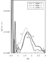
- the shortest inter-dot distance of semiconductor quantum dots can be obtained by structural evaluation of a quantum dot film having semiconductor quantum dots by a grazing incidence small angle X-ray scattering (GISAXS). . By such measurement, the center-to-center distance d between adjacent semiconductor quantum dots is obtained, and the shortest distance between dots is calculated by subtracting the particle diameter of the semiconductor quantum dots from the obtained center-to-center distance d.
- the average of the scattered X-rays for the semiconductor quantum dots existing in all the regions irradiated with the X-rays is detected as the measurement target scattered X-rays.
- the shortest dot-to-dot distance calculated based on the detected scattered X-rays is an “average shortest dot-to-dot distance” that is an average value of the shortest distances between dots.
- the photocurrent value of the semiconductor film can be improved as the average shortest distance between dots of the semiconductor quantum dots is smaller.
- the average shortest distance between dots is 0 nm, that is, the semiconductor quantum dots are in contact with each other, and the aggregated form is not different from the bulk semiconductor, and the characteristics of the semiconductor quantum dots that are nano-sized cannot be obtained.
- the average shortest distance between dots is preferably larger than 0 nm.
- the average shortest distance between dots of the semiconductor quantum dots is more preferably less than 0.30 nm, and further preferably less than 0.20 nm.
- the thickness of the semiconductor film is not particularly limited, but is preferably 10 nm or more and more preferably 50 nm or more from the viewpoint of obtaining high electrical conductivity. In addition, the thickness of the semiconductor film is preferably 300 nm or less from the viewpoint of excessive carrier concentration and ease of manufacture.
- the manufacturing method of the semiconductor film of the present invention is not particularly limited, it is manufactured by the semiconductor film manufacturing method of the present invention from the viewpoint of shortening the interval between the semiconductor quantum dots and arranging the semiconductor quantum dots densely. It is preferable to do.
- a semiconductor quantum dot dispersion liquid containing a semiconductor quantum dot, a first ligand coordinated to the semiconductor quantum dot, and a first solvent is applied onto the substrate.
- the molecular chain length is shorter than that of the first ligand and the arrangement represented by the general formula (A)
- a second ligand and a second solvent which are at least one selected from a ligand, a ligand represented by formula (B), and a ligand represented by formula (C)
- X 1 represents —SH, —NH 2 , or —OH
- a 1 and B 1 each independently represent a hydrogen atom or a substituent having 1 to 10 atoms.
- X 1 represents —SH or —OH
- X 2 represents —SH, —NH 2 , or —OH
- a 2 and B 2 each independently represent a hydrogen atom or a substituent having 1 to 10 atoms.
- a 3 represents a hydrogen atom or atoms of 1 to 10 substituents.
- the semiconductor quantum dot assembly forming step and the ligand exchange step may be repeated, and further, a dispersion drying step for drying the semiconductor quantum dot dispersion, a ligand solution A solution drying step for drying the substrate, a washing step for washing the semiconductor quantum dot aggregate on the substrate, and the like.
- a semiconductor quantum dot dispersion is applied to the substrate to form an assembly of semiconductor quantum dots on the substrate.
- the semiconductor quantum dots are dispersed in the first solvent by the first ligand having a molecular chain length longer than that of the second ligand, the semiconductor quantum dots are less likely to be in an aggregated bulk shape. . Therefore, by applying the semiconductor quantum dot dispersion liquid onto the substrate, the semiconductor quantum dot aggregate can be configured so that the semiconductor quantum dots are arranged one by one.
- the first ligand coordinated to the semiconductor quantum dot and the first coordination by applying a solution of the specific ligand to the aggregate of semiconductor quantum dots by the ligand exchange step Ligand exchange is performed with a second ligand (specific ligand) having a molecular chain length shorter than that of the child.
- the specific ligand has an amino group in the molecule as shown in the general formulas (A) to (C). As described above, the amino group has a high complex stability constant.
- the metal atom of the semiconductor quantum dot and —SH represented by X 1 (or X 2 ) are used. , -NH 2 or -OH.
- the amino group is considered to promote the complex formation between the metal atom of the semiconductor quantum dot and the OH of the carboxy group. Therefore, the second ligand (specific ligand) is coordinated by replacing the first ligand having a molecular chain length longer than that of the second ligand, and the coordination bond with the semiconductor quantum dot. Therefore, it is considered that the semiconductor quantum dots are easily brought close to each other. When the semiconductor quantum dots are brought close to each other, it is considered that the electrical conductivity of the aggregate of semiconductor quantum dots is increased and a semiconductor film having a high photocurrent value can be obtained. Furthermore, it is considered that the semiconductor quantum dots are connected to each other by a coordinate bond through a specific ligand, whereby the aggregate of semiconductor quantum dots becomes a strong semiconductor film and hardly peels off from the substrate.
- a semiconductor quantum dot dispersion liquid containing a semiconductor quantum dot, a first ligand coordinated to the semiconductor quantum dot, and a first solvent is applied on the substrate to form the semiconductor quantum dot To form an aggregate.
- the semiconductor quantum dot dispersion liquid may be applied to the substrate surface, or may be applied to another layer provided on the substrate. Examples of other layers provided on the substrate include an adhesive layer and a transparent conductive layer for improving the adhesion between the substrate and the assembly of semiconductor quantum dots.
- the semiconductor quantum dot dispersion liquid contains a semiconductor quantum dot having a metal atom, a first ligand, and a first solvent.
- the semiconductor quantum dot dispersion liquid may further contain other components as long as the effects of the present invention are not impaired.
- the details of the semiconductor quantum dots containing metal atoms contained in the semiconductor quantum dot dispersion liquid are as described above, and the preferred embodiments are also the same.
- the content of the semiconductor quantum dots in the semiconductor quantum dot dispersion liquid is preferably 1 mg / ml to 100 mg / ml, and more preferably 5 mg / ml to 40 mg / ml. When the content of the semiconductor quantum dots in the semiconductor quantum dot dispersion liquid is 1 mg / ml or more, the semiconductor quantum dot density on the substrate is increased, and a good film is easily obtained.
- the content of the semiconductor quantum dots is 100 mg / ml or less
- the film thickness of the film obtained when the semiconductor quantum dot dispersion liquid is applied once is hardly increased. Therefore, the ligand exchange of the 1st ligand coordinated to the semiconductor quantum dot in a film
- membrane can fully be performed.
- the first ligand contained in the semiconductor quantum dot dispersion liquid functions as a ligand coordinated to the semiconductor quantum dot and has a molecular structure that is likely to cause steric hindrance, and the semiconductor quantum in the first solvent. It also serves as a dispersant for dispersing dots.
- the first ligand has a longer molecular chain length than the second ligand described later. The length of the molecular chain is determined by the length of the main chain when there is a branched structure in the molecule.
- “dispersion” refers to a state where there is no sedimentation or turbidity of particles.
- the first ligand is preferably a ligand having at least 6 carbon atoms in the main chain, and a ligand having 10 or more carbon atoms in the main chain. Is more desirable.
- the first ligand may be either a saturated compound or an unsaturated compound. Decanoic acid, lauric acid, myristic acid, palmitic acid, stearic acid, behenic acid, oleic acid, erucic acid, oleylamine , Dodecylamine, dodecanethiol, 1,2-hexadecanethiol, trioctylphosphine oxide, cetrimonium bromide and the like.
- the first ligand is preferably one that hardly remains in the film when the semiconductor film is formed.
- the first ligand is preferably at least one of oleic acid and oleylamine, from the viewpoint of making the semiconductor quantum dots have dispersion stability and hardly remaining in the semiconductor film.
- the content of the first ligand in the semiconductor quantum dot dispersion is preferably 10 mmol / l to 200 mmol / l with respect to the total volume of the semiconductor quantum dot dispersion.
- the first solvent contained in the semiconductor quantum dot dispersion liquid is not particularly limited, but is preferably a solvent that hardly dissolves the semiconductor quantum dots and easily dissolves the first ligand.
- the first solvent is preferably an organic solvent, and specific examples include alkanes [n-hexane, n-octane, etc.], benzene, toluene and the like. Only 1 type may be sufficient as a 1st solvent and the mixed solvent which mixed 2 or more types may be sufficient as it.
- the first solvent is preferably a solvent that hardly remains in the formed semiconductor film. If the solvent has a relatively low boiling point, the content of residual organic substances can be suppressed when the semiconductor film is finally obtained. Furthermore, those with good wettability to the substrate are naturally preferable. For example, when coating on a glass substrate, alkanes such as hexane and octane are more preferable.
- the content of the first solvent in the semiconductor quantum dot dispersion is preferably 90% by mass to 98% by mass with respect to the total mass of the semiconductor quantum dot dispersion.
- the semiconductor quantum dot dispersion is applied on the substrate.
- the structure of the substrate may be a single layer structure or a laminated structure.
- a substrate made of glass, an inorganic material such as YSZ (Yttria-Stabilized Zirconia), a resin, a resin composite material, or the like can be used as the substrate.
- a substrate made of a resin or a resin composite material is preferable from the viewpoint of light weight and flexibility.
- Resins include polybutylene terephthalate, polyethylene terephthalate, polyethylene naphthalate, polybutylene naphthalate, polystyrene, polycarbonate, polysulfone, polyethersulfone, polyarylate, allyl diglycol carbonate, polyamide, polyimide, polyamideimide, polyetherimide, poly Fluorine resins such as benzazole, polyphenylene sulfide, polycycloolefin, norbornene resin, polychlorotrifluoroethylene, liquid crystal polymer, acrylic resin, epoxy resin, silicone resin, ionomer resin, cyanate resin, crosslinked fumaric acid diester, cyclic polyolefin, aromatic Synthetic resins such as aromatic ethers, maleimide-olefins, cellulose, episulfide compounds, etc. .
- a composite plastic material of a resin and the following inorganic material can be given. That is, composite plastic material of resin and silicon oxide particles, composite plastic material of resin and metal nanoparticles, composite plastic material of resin and inorganic oxide nanoparticles, composite plastic material of resin and inorganic nitride nanoparticles, Composite plastic material of resin and carbon fiber, composite plastic material of resin and carbon nanotube, composite plastic material of resin and glass flake, composite plastic material of resin and glass fiber, composite plastic material of resin and glass beads, Composite plastic material of resin and clay mineral, Composite plastic material of resin and particles having mica derivative crystal structure, Laminated plastic material having at least one bonding interface between resin and thin glass, Inorganic layer and organic layer By laminating alternately, at least one or more Composite material or the like having a barrier property with the bonding interface.
- an aluminum substrate or an aluminum substrate with an oxide film whose surface insulation is improved by subjecting the surface to oxidation treatment (for example, anodization treatment). Also good.
- a substrate made of resin or resin composite material is excellent in heat resistance, dimensional stability, solvent resistance, electrical insulation, workability, low air permeability, low moisture absorption, etc. It is preferable.
- the resin substrate and the resin composite material substrate may include a gas barrier layer for preventing permeation of moisture, oxygen, etc., an undercoat layer for improving the flatness of the resin substrate and the adhesion to the lower electrode, and the like. Good.
- a lower electrode, an insulating film, or the like may be provided on the substrate. In that case, a semiconductor quantum dot dispersion liquid is applied to the lower electrode or the insulating film on the substrate.
- the thickness of the substrate is not particularly limited, but is preferably 50 ⁇ m to 1000 ⁇ m, and more preferably 50 ⁇ m to 500 ⁇ m.
- the thickness of the substrate is 50 ⁇ m or more, the flatness of the substrate itself is improved, and when the thickness of the substrate is 1000 ⁇ m or less, the flexibility of the substrate itself is improved and the semiconductor film can be used as a flexible semiconductor device. It becomes easier.
- the method for applying the semiconductor quantum dot dispersion on the substrate is not particularly limited, and examples thereof include a method of applying the semiconductor quantum dot dispersion on the substrate, a method of immersing the substrate in the semiconductor quantum dot dispersion, and the like. More specifically, as a method of applying the semiconductor quantum dot dispersion liquid on the substrate, spin coating method, dipping method, ink jet method, dispenser method, screen printing method, letterpress printing method, intaglio printing method, spray coating method, etc. The liquid phase method can be used.
- the inkjet method, the dispenser method, the screen printing method, the relief printing method, and the intaglio printing method can form a coating film at an arbitrary position on the substrate and do not require a patterning step after the film formation. Therefore, the process cost can be reduced.
- the semiconductor quantum dot aggregate formed on the substrate by the semiconductor quantum dot aggregate formation step has a molecular chain length shorter than that of the first ligand, and a general formula (A ), A ligand represented by the general formula (B), and a second ligand that is at least one selected from a ligand represented by the general formula (C) And a solution containing the second solvent, the first ligand coordinated to the semiconductor quantum dots as the second ligand (specific ligand) contained in the ligand solution Exchange.
- the ligand solution contains at least a second ligand (specific ligand) and a second solvent.
- the ligand solution may further contain other components as long as the effects of the present invention are not impaired.
- the second ligand is the specific ligand described above, and the molecular chain length is shorter than that of the first ligand.
- the method for determining the length of the molecular chain length of the ligand is as described in the description of the first ligand.
- the details of the specific ligand are also as described above.
- a specific ligand has a hydroxyl group (OH) in a molecule
- OH hydroxyl group
- numerator When the specific ligand has a hydroxy group in the molecular structure, miscibility with alcohol can be increased.
- when performing ligand exchange of a semiconductor quantum dot by the ligand solution containing the specific ligand which has a hydroxyl group when alcohol is used as a 2nd solvent, ligand exchange is efficiently performed. It can be carried out.
- the content of the specific ligand in the ligand solution is preferably 5 mmol / l to 200 mmol / l, more preferably 10 mmol / l to 100 mmol / l with respect to the total volume of the ligand solution. .
- the second solvent contained in the ligand solution is not particularly limited, but is preferably a solvent that easily dissolves the specific ligand.
- a solvent is preferably an organic solvent having a high dielectric constant, and examples thereof include ethanol, acetone, methanol, acetonitrile, dimethylformamide, dimethyl sulfoxide, butanol, and propanol. Only 1 type may be sufficient as a 2nd solvent, and the mixed solvent which mixed 2 or more types may be sufficient as it.
- the second solvent is preferably a solvent that hardly remains in the formed semiconductor film. From the viewpoint of easy drying and easy removal by washing, an alcohol or alkane having a low boiling point is preferable, and methanol, ethanol, n-hexane, or n-octane is more preferable.
- the second solvent is preferably not mixed with the first solvent.
- the second solvent is methanol or acetone. It is preferable to use a polar solvent such as
- content of the 2nd solvent in a ligand solution is the remainder which deducted content of the specific ligand from the ligand solution total mass.
- the method of applying the ligand solution to the aggregate of semiconductor quantum dots is the same as the method of applying the semiconductor quantum dot dispersion on the substrate, and the preferred embodiment is also the same.
- the semiconductor quantum dot assembly forming step and the ligand exchange step may be repeated.
- the electrical conductivity of the semiconductor film having an assembly of semiconductor quantum dots coordinated with a specific ligand is increased, and the thickness of the semiconductor film is increased. Can be thickened.
- the semiconductor quantum dot assembly formation step and the ligand exchange step may be repeated separately, but the ligand exchange step is performed after the semiconductor quantum dot assembly formation step is performed. It is preferable to repeat the cycle.
- By repeating the set of the semiconductor quantum dot assembly forming step and the ligand exchange step unevenness of ligand exchange can be easily suppressed.
- the photocurrent value of the semiconductor film increases as the exchange rate of the semiconductor quantum dot aggregate to the specific ligand in the ligand exchange increases.
- the ligand exchange between the first ligand and the second ligand (specific ligand) of the semiconductor quantum dot is performed in at least a part of the semiconductor quantum dot assembly. , 100% (number) may not replace the specific ligand.
- the manufacturing method of the semiconductor film of this invention may have the washing
- the washing step excess ligands and ligands desorbed from the semiconductor quantum dots can be removed. Further, the remaining solvent and other impurities can be removed.
- the cleaning of the semiconductor quantum dot aggregate is performed by pouring at least one of the first solvent and the second solvent on the semiconductor quantum dot aggregate, or by removing the substrate on which the semiconductor quantum dot aggregate or the semiconductor film is formed. What is necessary is just to immerse in at least one of 1 solvent and 2nd solvent.
- the cleaning by the cleaning process may be performed after the semiconductor quantum dot assembly forming process or may be performed after the ligand exchange process. Moreover, you may carry out after the repetition of the set of a semiconductor quantum dot aggregate formation process and a ligand exchange process.
- the manufacturing method of the semiconductor film of this invention may have a drying process.
- the drying step may be a dispersion drying step for drying the solvent remaining in the semiconductor quantum dot assembly after the semiconductor quantum dot assembly forming step, or the ligand solution may be replaced with a ligand solution after the ligand exchange step. It may be a solution drying step for drying.
- the comprehensive process performed after the repetition of the set of a semiconductor quantum dot aggregate formation process and a ligand exchange process may be sufficient.
- a semiconductor film is manufactured on the substrate through the steps described above. Since the obtained semiconductor film is formed by connecting semiconductor quantum dots with a specific ligand shorter than the conventional one, the electrical conductivity is high and a high photocurrent value is obtained. In addition, since the specific ligand has a high complex stability constant, the semiconductor film of the present invention composed of the semiconductor quantum dots and the specific ligand has stable coordination bonds, excellent film strength, Peeling is also suppressed.
- the semiconductor film of the present invention has photoelectric conversion characteristics and hardly peels off, and thus can be suitably applied to various electronic devices having a semiconductor film or a photoelectric conversion film.
- the semiconductor film of the present invention includes a photoelectric conversion film of a solar cell, a light emitting diode (LED), a semiconductor layer (active layer) of a thin film transistor, a photoelectric conversion film of an indirect radiation imaging apparatus, and a visible to infrared region. It can be suitably applied to a photodetector or the like.
- a solar cell will be described as an example of an electronic device including the semiconductor film of the present invention or the semiconductor film manufactured by the method of manufacturing a semiconductor film of the present invention.
- a pn junction solar cell can be obtained by using a semiconductor film device having a pn junction including a p-type semiconductor layer including the semiconductor film of the present invention and an n-type semiconductor layer.
- a pn junction solar cell for example, a p-type semiconductor layer and an n-type semiconductor layer are provided adjacent to each other on a transparent conductive film formed on a transparent substrate.
- a form in which a metal electrode is formed on the n-type semiconductor layer is exemplified.
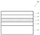
- FIG. 1 shows a schematic cross-sectional view of a pn junction solar cell 100 according to an embodiment of the present invention.
- a pn junction solar cell 100 includes a transparent substrate 10, a transparent conductive film 12 provided on the transparent substrate 10, a p-type semiconductor layer 14 formed of the semiconductor film of the present invention on the transparent conductive film 12, and p An n-type semiconductor layer 16 and a metal electrode 18 provided on the n-type semiconductor layer 16 are stacked on the type semiconductor layer 14.
- the p-type semiconductor layer 14 and the n-type semiconductor layer 16 are laminated adjacent to each other, a pn junction solar cell can be obtained.
- the transparent substrate 10 the same material as the substrate used in the method for producing a semiconductor film of the present invention can be used as long as it is transparent. Specifically, a glass substrate, a resin substrate, etc. are mentioned.
- the transparent conductive film 12 includes a film composed of In 2 O 3 : Sn (ITO), SnO 2 : Sb, SnO 2 : F, ZnO: Al, ZnO: F, CdSnO 4 and the like. .
- the n-type semiconductor layer 16 is preferably a metal oxide. Specific examples include metal oxides containing at least one of Ti, Zn, Sn, and In, and more specific examples include TiO 2 , ZnO, SnO 2 , and IGZO.
- the n-type semiconductor layer is preferably formed by a wet method (also referred to as a liquid phase method) in the same manner as the p-type semiconductor layer from the viewpoint of manufacturing cost.
- a wet method also referred to as a liquid phase method
- the metal electrode 18 Pt, Al, Cu, Ti, Ni, or the like can be used.
- PbS particle dispersion 1 a PbS particle dispersion in which PbS particles were dispersed in toluene was prepared.
- PbS core Evidot nominal particle size 3.3 nm, 20 mg / ml, solvent toluene
- 2 ml of the PbS particle dispersion was taken into the centrifuge tube, 38 ⁇ l of oleic acid was added, and then 20 ml of toluene was added to dilute the concentration of the dispersion.
- the obtained dispersion was concentrated using a rotary evaporator (35 hpa, 40 ° C.), and as a result, about 4 ml of semiconductor quantum dot dispersion 1 (octane solvent) having a concentration of about 10 mg / ml was obtained.
- the average particle diameter of the PbS particles contained in the semiconductor quantum dot dispersion liquid 1 was 3 nm.
- the average particle diameter of the semiconductor quantum dots was calculated as an average of 10 semiconductor quantum dots by photographic observation in TEM (Transmission Electron Microscope) measurement. A TEI 80-300 manufactured by FEI Co. was used as a measuring device.
- the product was taken out from the three-necked round bottom flask, and unreacted products and by-products were removed by centrifugation using a centrifuge.
- the product (InP particles) was purified using ultra-dehydrated toluene as a good solvent and dehydrated ethanol as a poor solvent. Specifically, the process of dissolving the product in a good solvent, redispersing the dissolved InP particles in a poor solvent, and centrifuging the resulting InP particle dispersion was repeated. An ultrasonic cleaner was used for redispersion. After repeated centrifugation of the InP particle dispersion, dehydrated ethanol remaining in the InP particle dispersion was removed by distillation under reduced pressure using a rotary evaporator.
- the extracted InP particles were dispersed in octane to obtain an octane dispersion having an oleylamine-modified InP particle concentration of 1 mg / ml. This was designated as semiconductor quantum dot dispersion 2.
- the three-necked flask is cooled to room temperature and aerated with nitrogen gas, and then a solution containing 2.57 mmol of hexamethyldisilazian and 5 ml of 1-octadecene is injected into the three-necked flask with a syringe.
- the septum cap was stabbed with a syringe needle and injected).
- the three-necked flask was heated to 120 ° C. over 40 minutes and held for 1 minute, and then the three-necked flask was cooled to room temperature with a cooling fan.
- a substrate having 65 pairs of comb-shaped platinum electrodes shown in FIG. 2 on a quartz glass was prepared.
- a comb-type platinum electrode (model number 012126, electrode interval 5 ⁇ m) manufactured by BAS was used.
- Table 1 shows the combinations of the semiconductor quantum dot dispersion liquid and the ligand solution in Examples and Comparative Examples.
- PbS in the “seed” column of the “semiconductor quantum dot” column means that the semiconductor quantum dot dispersion liquid 1 was used
- InP means that the semiconductor quantum dot dispersion liquid 2 was used.
- the types of ligands contained in the ligand solution are the ligands shown in the “Compound Name” column of the “Ligand” column of Table 1.
- A in the “ligand”, “general formula”, and “seed” columns means that the ligand is represented by the general formula (A), and “B” means that the ligand is represented by the general formula. It means that it is represented by (B), and “C” means that the ligand is represented by the general formula (C).
- Ligands that cannot be represented by the general formulas (A), (B), and (C) are represented by “ ⁇ ”. “Number of A” represents the number of atoms of A 1 , A 2 or A 3 , and “Number of B” represents the number of atoms of B 1 or B 2 .
- the ligand used in Comparative Example 4 is potassium bromide (KBr), and the ligand used in Comparative Example 5 is cetyltrimethylammonium bromide [(CH 3 (CH 2 ) 15 N ( CH 3 ) 3 ) + , Br ⁇ ].
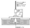
- the electrical conductivity of the semiconductor film was evaluated by using a semiconductor parameter analyzer for the produced semiconductor film device. First, the voltage applied to the electrodes was swept between ⁇ 5 to 5 V without irradiating the semiconductor film device with light, and the IV characteristics in the dark state were obtained. The current value with a +5 V bias applied was adopted as the dark current value Id. Next, to evaluate the photocurrent values while irradiating monochromatic light (irradiation intensity 10 13 photons) to the semiconductor film device. The semiconductor film device was irradiated with monochrome light using the apparatus shown in FIG. The wavelength of the monochromatic light was systematically changed between 280 nm and 700 nm. The increase in current from the dark current when irradiating light with a wavelength of 280 nm was taken as the photocurrent value Ip. The evaluation results are shown in Table 1.
- the electrical conductivity of the semiconductor film is improved by bringing the semiconductor quantum dots close to each other using a specific ligand. can do.
- the semiconductor quantum dots are too close to each other, the semiconductor quantum dots are likely to be aggregated.
- Semiconductor quantum dots are expected to become bulky when aggregated.
- the semiconductor film desirably retains physical properties as a semiconductor quantum dot while exhibiting good electrical characteristics. In particular, when considering application of a semiconductor film to an LED or a solar cell, it is difficult to obtain absorption and emission of a target wavelength unless the semiconductor film has physical properties as a semiconductor quantum dot.
- the film of Comparative Example 11 was obtained in the same manner as in Example 1 except that the ligand solution obtained in the same manner as in Example 1 except that the ligand was changed to glycolic acid. It is.
- the film of Comparative Example 12 is a film obtained in Example 1 without performing the steps (2) and (3) among the steps (1) to (4) in “Manufacturing the semiconductor film”. .
- the film of Comparative Example 12 was an insulating film that did not exhibit electrical conductivity because the semiconductor quantum dots were not close to each other.
- the PbS bulk is a general II-VI group semiconductor, which is a single crystal of PbS, has a size larger than 100 nm, and has no quantum size effect.
- FIG. 6 An experimental setup used for photoluminescence measurement is schematically shown in FIG.
- This experimental apparatus mainly includes a laser irradiator 20, a total reflection mirror 22, a dichroic mirror 24, lenses 26 and 28, and a spectroscope 32.
- the laser light emitted from the laser irradiator 20 is converted into a total reflection mirror 22,
- the structure reaches the measurement sample (semiconductor film of the evaluation device) 30 and the spectroscope 32 through the dichroic mirror 24 and the lenses 26 and 28, respectively.
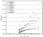
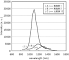
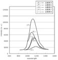
- 6 to 8 show PL spectra.
- FIG. 6 shows PL spectra of Example 1 (curve A), Example 2 (curve B), and Comparative Example 12 (curve C).
- FIG. 6 shows PL spectra of Example 1 (curve A), Example 2 (curve B), and Comparative Example 12 (curve C).
- FIG. 7 shows the PL spectra of Comparative Example 1 (curve D) and Comparative Example 12 (curve C), and FIG. 8 shows the PL spectra of Comparative Examples 4 to 8 (curve E to curve I).
- the peak wavelengths in each ligand are summarized in Table 2.
- the peak wavelength of the PbS semiconductor quantum dots (Comparative Example 12) in which oleic acid was coordinated without ligand exchange was about 1100 nm.
- the semiconductor film excluding the semiconductor film coordinated with 2-aminoethane-1-thiol (Example 1), it can be seen that the peak wavelength is shifted to the long wave side by about 60 nm to 120 nm.
- the shift of the peak wavelength to the long wavelength side is because the confinement potential of the semiconductor quantum dots is reduced due to the proximity of the semiconductor quantum dots by ligand exchange, and the band gap is effectively reduced. is there.
- the decrease in the band gap is the largest and is about 100 meV.
- Example 1 and Example 2 the semiconductor film of semiconductor quantum dots coordinated with a specific ligand has a short semiconductor quantum dot interval and high electrical conduction through the semiconductor quantum dots. While exhibiting the characteristics, it was confirmed that the physical properties (band gap, etc.) of the semiconductor quantum dots were retained.
- the peak wavelength appears in the vicinity of 1290 nm for the semiconductor film of the semiconductor quantum dots coordinated with 2-aminoethanethiol (Example 1).
- the emission peak of the semiconductor film of Example 1 is different from the emission peak of the bulk and the emission peak of the normal semiconductor quantum dot, and the energy level of the semiconductor quantum dot is modulated when the semiconductor quantum dots are very close to each other. This result suggests the formation of a new energy level.
- Average particle diameter of semiconductor quantum dots The average particle diameter of the semiconductor quantum dots was measured with a TEM apparatus. As a measuring apparatus, TITAN 80-300 manufactured by FEI was used. Two types of samples were prepared. One is a sample obtained by drop-casting the semiconductor quantum dot dispersion 1 on a Si substrate, collected by a sampling knife, and placed on a measurement stage. The other is that a spin coat film having undergone ligand exchange with ethanedithiol is formed on a quartz glass substrate, and is similarly collected with a sampling knife. In other words, the latter sample is a semiconductor film obtained in the same manner except that a quartz glass substrate was used as the substrate in the production of the semiconductor film of Comparative Example 1.
- FIG. 9 shows a TEM image when the semiconductor quantum dot dispersion liquid 1 is drop-cast. From FIG. 9, it was confirmed that the average particle diameter (average of 10 dots) of the quantum dots was 3 nm. In addition, since the oleic acid, which is a long chain fatty acid, remains coordinated without ligand exchange, it can be seen that the interval between the semiconductor quantum dots is very wide (2 nm to 4 nm).
- FIG. 1 a TEM image of the spin coat film after ligand exchange is shown in FIG.
- the semiconductor film of the present invention in which the specific ligand is coordinated to the semiconductor quantum dots is the proximity of the semiconductor quantum dots.
- Example 12 The structure of the obtained quantum dot films (samples) of Example 12, Example 13, Comparative Example 14, and Comparative Example 15 was evaluated by a small angle incident X-ray small angle scattering method (GISAXS).
- the incident light is Cu K ⁇ rays
- the quantum dot film is irradiated with X-rays at an incident angle (about 0.4 °) slightly larger than the total reflection angle, and the detector is scanned in the in-plane direction. Scattered light was detected.
- FIG. 11 shows the in-plane angle dependence of the scattered light obtained by subtracting the background structure of the scattered light with respect to each ligand type for the semiconductor films of Example 12, Example 13, and Comparative Example 14.
- ⁇ is the wavelength of incident light.
- Table 3 shows the shortest distance between adjacent quantum dots calculated from the scattering peak (the measured distance between centers of quantum dots d minus the particle diameter of the quantum dots).
- the detected scattered light is an average of scattered X-rays for samples present in all regions irradiated with X-rays in the measurement apparatus.
- the average shortest distance between dots is smaller than the conventional semiconductor film coordinated with ethanedithiol (less than 0.45 nm) It was found that a high photocurrent value and a high dark current value can be obtained.
- the semiconductor film coordinated with ethanedithiol remarkable film peeling occurred with the naked eye, whereas for the semiconductor film coordinated with the specific ligand of the example, no film peeling was observed and good Roughness was realized.
- the average shortest distance between dots is preferably less than 0.3 nm, more preferably 2-aminoethane. As in the case of -1-thiol coordination, it has been found that the average shortest distance between dots is preferably less than 0.2 nm.
Landscapes
- Chemical & Material Sciences (AREA)
- Engineering & Computer Science (AREA)
- Nanotechnology (AREA)
- Crystallography & Structural Chemistry (AREA)
- Physics & Mathematics (AREA)
- Organic Chemistry (AREA)
- Condensed Matter Physics & Semiconductors (AREA)
- General Physics & Mathematics (AREA)
- Manufacturing & Machinery (AREA)
- Materials Engineering (AREA)
- Theoretical Computer Science (AREA)
- Composite Materials (AREA)
- Mathematical Physics (AREA)
- General Health & Medical Sciences (AREA)
- Molecular Biology (AREA)
- Biochemistry (AREA)
- Life Sciences & Earth Sciences (AREA)
- Health & Medical Sciences (AREA)
- Photovoltaic Devices (AREA)
- Electroluminescent Light Sources (AREA)
- Thin Film Transistor (AREA)
Abstract
金属原子を有する半導体量子ドットの集合体と、半導体量子ドットに配位し、一般式(A)で表される配位子、一般式(B)で表される配位子、および一般式(C)で表される配位子から選択される少なくとも1種の配位子と、を有する半導体膜。〔一般式(A)中、X1は、-SH、-NH2、または、-OHを表し、A1及びB1は、各々独立に、水素原子または原子数1以上10以下の置換基を表す。但し、A1及びB1が共に水素原子のときは、X1は-SH、または、-OHを表す。 一般式(B)中、X2は、-SH、-NH2、または、-OHを表し、A2及びB2は、各々独立に、水素原子または原子数1以上10以下の置換基を表す。 一般式(C)中、A3は、水素原子または原子数1以上10以下の置換基を表す。〕
Description
本発明は、半導体膜、半導体膜の製造方法、太陽電池、発光ダイオード、薄膜トランジスタ、および、電子デバイスに関する。
近年、第三世代太陽電池と呼ばれる高効率太陽電池の研究が盛んである。その中でもコロイド量子ドットを用いた太陽電池は、例えば、マルチエキシトン生成効果により量子効率を高められる事が報告されており、注目を集めている。しかし、コロイド量子ドットを用いた太陽電池(量子ドット太陽電池とも称される)では、変換効率が最大でも7%程度であり、更なる変換効率の向上が求められている。
このような量子ドット太陽電池では、量子ドットの集合体からなる半導体膜が光電変換層を担っていることから、量子ドットの集合体からなる半導体膜自体の研究も盛んに行われている。
例えば、炭化水素基の炭素数が6以上の比較的長い配位子を用いた半導体ナノ粒子が開示されている(例えば、特許文献1(特許第4425470号)参照)。
量子ドットの集合体からなる半導体膜の特性を改善する手法としては、量子ドット(例えば2nm~10nm程度)に結合している配位子分子をより短い配位子分子に置換する事で、電気伝導性が向上することが報告されている(例えば、非特許文献1(S.Geyerら著、「Charge transport in mixed CdSe and CdTe colloidal nanocrystal films」、Physical Review B(2010))、及び非特許文献2(J. M. Lutherら著。「Structural, Optical, and Electrical Properties of Self-Assembled Films of PbSe Nanocrystals Treated with 1,2-Ethanedithiol」、ACS Nano (2008))参照)。非特許文献2では、PbSeの量子ドットの周囲のオレイン酸(分子鎖長2nm~3nm程度)をエタンジチオール(分子鎖長1nm以下)に置換する事によって量子ドット同士が近接化し、電気伝導性が向上することが報告されている。
しかし、特許文献1に記載される半導体膜は、配位子が大きく、半導体量子ドット同士の近接化が不十分であるため、光電変換特性に優れなかった。また、非特許文献1で用いられているブチルアミン、または、非特許文献2で用いられているエタンジチオールを配位子として用いた場合でも、例えば、非特許文献1によれば、最大でも数百nA程度の光電流値しか得ることができていない。また、配位子としてエタンジチオールを用いると、半導体膜の膜剥がれが生じ易かった。
本発明は、高い光電流値が得られ、かつ、膜剥がれが抑制される半導体膜およびその製造方法を提供することを課題とし、かかる課題を解決することを目的とする。
また、高い光電流値が得られ、かつ膜剥がれが抑制される太陽電池、発光ダイオード、薄膜トランジスタ、および、電子デバイスを提供することを課題とし、かかる課題を解決することを目的とする。
また、高い光電流値が得られ、かつ膜剥がれが抑制される太陽電池、発光ダイオード、薄膜トランジスタ、および、電子デバイスを提供することを課題とし、かかる課題を解決することを目的とする。
上記目的を達成するため、以下の発明が提供される。
<1> 金属原子を有する半導体量子ドットの集合体と、半導体量子ドットに配位し、一般式(A)で表される配位子、一般式(B)で表される配位子、および一般式(C)で表される配位子からなる群から選択される少なくとも1種の配位子と、を有する半導体膜である。
<1> 金属原子を有する半導体量子ドットの集合体と、半導体量子ドットに配位し、一般式(A)で表される配位子、一般式(B)で表される配位子、および一般式(C)で表される配位子からなる群から選択される少なくとも1種の配位子と、を有する半導体膜である。

一般式(A)中、X1は、-SH、-NH2、または、-OHを表し、A1及びB1は、各々独立に、水素原子または原子数1以上10以下の置換基を表す。但し、A1及びB1が共に水素原子のときは、X1は-SH、または、-OHを表す。
一般式(B)中、X2は、-SH、-NH2、または、-OHを表し、A2及びB2は、各々独立に、水素原子または原子数1以上10以下の置換基を表す。
一般式(C)中、A3は、水素原子または原子数1以上10以下の置換基を表す。
一般式(B)中、X2は、-SH、-NH2、または、-OHを表し、A2及びB2は、各々独立に、水素原子または原子数1以上10以下の置換基を表す。
一般式(C)中、A3は、水素原子または原子数1以上10以下の置換基を表す。
<2> A1、B1、A2、B2、及びA3が、各々独立に、水素原子または原子数7以下の置換基である<1>に記載の半導体膜である。
<3> A1、B1、A2、B2、及びA3が、水素原子である<1>または<2>に記載の半導体膜である。
<4> 少なくとも1種の配位子が、2-アミノエタンチオール、2-アミノエタノール、3-アミノ-1-プロパノール、2-アミノエタンチオール誘導体、2-アミノエタノール誘導体、及び3-アミノ-1-プロパノール誘導体からなる群から選択される少なくとも1種である<1>~<3>のいずれか1つに記載の半導体膜である。
<5> 少なくとも1種の配位子は、一般式(A)で表され、半導体量子ドット中の金属原子と共に、5員環キレートを形成する<1>~<4>のいずれか1つに記載の半導体膜である。
<6> 少なくとも1種の配位子と半導体量子ドットの金属原子との間の錯安定度定数logβ1が8以上である<1>~<5>のいずれか1つに記載の半導体膜である。
<7> 半導体量子ドットは、ドット間平均最短距離が0.45nm未満である<1>~<6>のいずれか1つに記載の半導体膜である。
<8> 半導体量子ドットは、ドット間平均最短距離が0.30nm未満である<7>に記載の半導体膜である。
<9> 半導体量子ドットは、ドット間平均最短距離が0.20nm未満である<7>または<8>に記載の半導体膜である。
<10> 半導体量子ドットは、PbS、PbSe、InN、InAs、InSb、及びInPからなる群から選択される少なくとも1つを含む<1>~<9>のいずれか1つに記載の半導体膜である。
<11> 半導体量子ドットは、平均粒径が2nm~15nmである<1>~<10>のいずれか1つに記載の半導体膜である。
<12> 半導体量子ドットは、PbSを含む<10>または<11>に記載の半導体膜である。
<13> 金属原子を含む半導体量子ドット、半導体量子ドットに配位した第1の配位子、及び第1の溶媒を含有する半導体量子ドット分散液を基板上に付与して半導体量子ドットの集合体を形成する半導体量子ドット集合体形成工程と、半導体量子ドットの集合体に、第1の配位子よりも分子鎖長が短く、かつ、下記一般式(A)で表される配位子、下記一般式(B)で表される配位子、および下記一般式(C)で表される配位子からなる群から選択される少なくとも1種である第2の配位子及び第2の溶媒を含有する溶液を付与して半導体量子ドットに配位している第1の配位子を第2の配位子に交換する配位子交換工程と、を有する半導体膜の製造方法である。

一般式(A)中、X1は、-SH、-NH2、または、-OHを表し、A1及びB1は、各々独立に、水素原子または原子数1以上10以下の置換基を表す。但し、A1及びB1が共に水素原子のときは、X1は-SH、または、-OHを表す。
一般式(B)中、X2は、-SH、-NH2、または、-OHを表し、A2及びB2は、各々独立に、水素原子または原子数1以上10以下の置換基を表す。
一般式(C)中、A3は、水素原子または原子数1以上10以下の置換基を表す。
一般式(B)中、X2は、-SH、-NH2、または、-OHを表し、A2及びB2は、各々独立に、水素原子または原子数1以上10以下の置換基を表す。
一般式(C)中、A3は、水素原子または原子数1以上10以下の置換基を表す。
<14> 第1の配位子は、主鎖の炭素数が6以上の配位子である<13>に記載の半導体膜の製造方法である。
<15> 半導体量子ドット集合体形成工程と、配位子交換工程と、をそれぞれ2回以上行う<13>または<14>に記載の半導体膜の製造方法である。
<16> A1、B1、A2、B2、及びA3が、各々独立に、水素原子または原子数7以下の置換基である<13>~<15>のいずれか1つに記載の半導体膜の製造方法である。
<17> A1、B1、A2、B2、及びA3が、水素原子である<13>~<16>のいずれか1つに記載の半導体膜の製造方法である。
<18> 第2の配位子が、2-アミノエタンチオール、2-アミノエタノール、3-アミノ-1-プロパノール、2-アミノエタンチオール誘導体、2-アミノエタノール誘導体、及び3-アミノ-1-プロパノール誘導体からなる群から選択される少なくとも1種である<13>~<17>のいずれか1つに記載の半導体膜の製造方法である。
<19> 配位子交換工程では、第2の配位子が、一般式(A)で表され、半導体量子ドット中の金属原子と共に、5員環キレートを形成する<13>~<18>のいずれか1つに記載の半導体膜の製造方法である。
<20> 半導体量子ドットは、PbS、PbSe、InN、InAs、InSb、及びInPからなる群から選択される少なくとも1つを含む<13>~<19>のいずれか1つに記載の半導体膜の製造方法である。
<21> 半導体量子ドットは、平均粒径が2nm~15nmである<13>~<20>のいずれか1つに記載の半導体膜の製造方法である。
<22> 半導体量子ドットは、PbSを含む<20>または<21>に記載の半導体膜の製造方法である。
<23> <1>~<12>のいずれか1つに記載の半導体膜を備える太陽電池である。
<24> <1>~<12>のいずれか1つに記載の半導体膜を備える発光ダイオードである。
<25> <1>~<12>のいずれか1つに記載の半導体膜を備える薄膜トランジスタである。
<26> <1>~<12>のいずれか1つに記載の半導体膜を備える電子デバイスである。
本発明によれば、高い光電流値が得られ、かつ膜剥がれが抑制される半導体膜およびその製造方法が提供される。
また、本発明によれば、高い光電流値が得られ、かつ膜剥がれが抑制される太陽電池、発光ダイオード、薄膜トランジスタ、および、電子デバイスが提供される。
また、本発明によれば、高い光電流値が得られ、かつ膜剥がれが抑制される太陽電池、発光ダイオード、薄膜トランジスタ、および、電子デバイスが提供される。
以下、本発明の半導体膜及びその製造方法について、詳細に説明する。
<半導体膜>
本発明の半導体膜は、金属原子を有する半導体量子ドットの集合体と、半導体量子ドットに配位し、一般式(A)で表される配位子、一般式(B)で表される配位子、および一般式(C)で表される配位子から選択される少なくとも1種の配位子と、を有する。
以下、「一般式(A)で表される配位子、一般式(B)で表される配位子、および一般式(C)で表される配位子から選択される少なくとも1種の配位子」を「特定配位子」とも称する。
本発明の半導体膜は、金属原子を有する半導体量子ドットの集合体と、半導体量子ドットに配位し、一般式(A)で表される配位子、一般式(B)で表される配位子、および一般式(C)で表される配位子から選択される少なくとも1種の配位子と、を有する。
以下、「一般式(A)で表される配位子、一般式(B)で表される配位子、および一般式(C)で表される配位子から選択される少なくとも1種の配位子」を「特定配位子」とも称する。
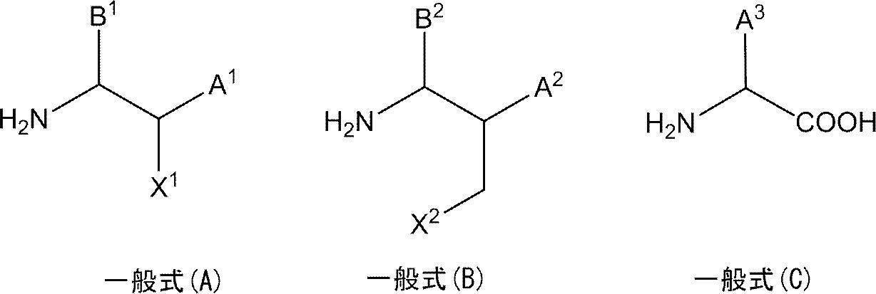
一般式(A)中、X1は、-SH、-NH2、または、-OHを表し、A1及びB1は、各々独立に、水素原子または原子数1以上10以下の置換基を表す。但し、A1及びB1が共に水素原子のときは、X1は-SH、または、-OHを表す。
一般式(B)中、X2は、-SH、-NH2、または、-OHを表し、A2及びB2は、各々独立に、水素原子または原子数1以上10以下の置換基を表す。
一般式(C)中、A3は、水素原子または原子数1以上10以下の置換基を表す。
また、一般式(A)で表される配位子、一般式(B)で表される配位子、および一般式(C)で表される配位子は、互いに異なる配位子である。
一般式(B)中、X2は、-SH、-NH2、または、-OHを表し、A2及びB2は、各々独立に、水素原子または原子数1以上10以下の置換基を表す。
一般式(C)中、A3は、水素原子または原子数1以上10以下の置換基を表す。
また、一般式(A)で表される配位子、一般式(B)で表される配位子、および一般式(C)で表される配位子は、互いに異なる配位子である。
半導体量子ドットは、金属原子を含んで構成される半導体粒子であり、粒径が数nm~数十nmとなるナノサイズの粒子である。
本発明の半導体膜は、半導体量子ドットが、一般式(A)、(B)または(C)で表される原子数の少ない特定配位子によって配位結合で結ばれているため、半導体量子ドット間の間隔が短くなっていると考えられる。そのため、半導体量子ドットが緻密に並び、半導体量子ドット間の波動関数の重なりを強めることができると考えられる。その結果、電気伝導性が高まり、光電流値を高めることができると考えられる。
また、特定配位子は、分子内に少なくとも1つのアミノ基(NH2)と、X1(またはX2)で表される-SH、-NH2もしくは-OH、またはカルボキシ基のOHとを有している。アミノ基は、錯安定度定数が高く、半導体量子ドットの金属原子と、X1(またはX2)で表される-SH、-NH2もしくは-OH、またはカルボキシ基のOHとの錯体形成を促進するものと考えられる。その結果、半導体量子ドットと特定配位子との結びつきを強固なものとするため、半導体量子ドットと特定配位子とを含んで構成される半導体膜の剥がれを抑制するものと考えられる。
従って、本発明の半導体膜は、高い光電流値が得られ、かつ膜剥がれを抑制することができると考えられる。
本発明の半導体膜は、半導体量子ドットが、一般式(A)、(B)または(C)で表される原子数の少ない特定配位子によって配位結合で結ばれているため、半導体量子ドット間の間隔が短くなっていると考えられる。そのため、半導体量子ドットが緻密に並び、半導体量子ドット間の波動関数の重なりを強めることができると考えられる。その結果、電気伝導性が高まり、光電流値を高めることができると考えられる。
また、特定配位子は、分子内に少なくとも1つのアミノ基(NH2)と、X1(またはX2)で表される-SH、-NH2もしくは-OH、またはカルボキシ基のOHとを有している。アミノ基は、錯安定度定数が高く、半導体量子ドットの金属原子と、X1(またはX2)で表される-SH、-NH2もしくは-OH、またはカルボキシ基のOHとの錯体形成を促進するものと考えられる。その結果、半導体量子ドットと特定配位子との結びつきを強固なものとするため、半導体量子ドットと特定配位子とを含んで構成される半導体膜の剥がれを抑制するものと考えられる。
従って、本発明の半導体膜は、高い光電流値が得られ、かつ膜剥がれを抑制することができると考えられる。
本発明の半導体膜は、特定配位子と半導体量子ドットの金属原子との間の錯安定度定数logβ1が8以上であることが好ましい。
ここで、錯安定度定数は、配位子と配位結合の対象となる金属原子との関係で定まる定数であり、下記式(b)により表される。
ここで、錯安定度定数は、配位子と配位結合の対象となる金属原子との関係で定まる定数であり、下記式(b)により表される。

式(b)において、[ML]は、金属原子と配位子が結合した錯体のモル濃度を表し、[M]は配位結合に寄与することができる金属原子のモル濃度を表し、[L]は配位子のモル濃度を表す。
実際には一つの金属原子に複数の配位子が配位する場合もあるが、本発明では、一つの金属原子に一つの配位子分子が配位する場合の式(b)で表される錯安定度定数logβ1を、配位結合の強さの指標として規定する。
特定配位子と半導体量子ドットの金属原子との間の錯安定度定数logβ1は、8以上であることで錯体が形成され易くなる。
錯安定度定数logβ1は、半導体量子ドットと配位子との組み合わせにおいて、より高い方が望ましい。また、配位子がキレートのように多座配位するものであればより結合の強さを高めることが出来る。一般的に、配位結合の強さが高いほうが、従来の長分子鎖配位子が効率的に置換され、より高い電気伝導性を得易くなる。また、特定配位子の錯安定度定数logβ1の値は、半導体量子ドットを構成する半導体量子ドット材料が変わることで変動するが、特定配位子は、分子鎖長が短く且つ配位し易いため、種々の半導体量子ドット材料に適用可能である。
logβ1は、8以上であることがより好ましく、10以上であることがさらに好ましい。
特定配位子と半導体量子ドットの金属原子との間の錯安定度定数logβ1は、8以上であることで錯体が形成され易くなる。
錯安定度定数logβ1は、半導体量子ドットと配位子との組み合わせにおいて、より高い方が望ましい。また、配位子がキレートのように多座配位するものであればより結合の強さを高めることが出来る。一般的に、配位結合の強さが高いほうが、従来の長分子鎖配位子が効率的に置換され、より高い電気伝導性を得易くなる。また、特定配位子の錯安定度定数logβ1の値は、半導体量子ドットを構成する半導体量子ドット材料が変わることで変動するが、特定配位子は、分子鎖長が短く且つ配位し易いため、種々の半導体量子ドット材料に適用可能である。
logβ1は、8以上であることがより好ましく、10以上であることがさらに好ましい。
本発明の半導体膜における特定配位子と半導体量子ドットの金属原子との間の錯安定度定数logβ1の求め方としては、分光法、磁気共鳴分光法、ポテンショメトリー、溶解度測定、クロマトグラフィー、カロリメトリー、凝固点測定、蒸気圧測定、緩和測定、粘度測定、表面張力測定等がある。
本発明では様々な手法や研究機関からの結果がまとめられた、Sc-Database ver.5.85(Academic Software)(2010)を使用することで、錯安定度定数を定めた。logβ1がSc-Database ver.5.85に無い場合には、A.E.MartellとR.M.Smith著、Critical Stability Constantsに記載の値を用いる。Critical Stability Constantsにも、logβ1が記載されていない場合は、既述の測定方法を用いるか、錯安定度定数を計算するプログラムPKAS法(A.E.Martellら著、The Determination and Use of Stability Constants,VCH(1988))を用いて、logβ1を算出する。
以下、本発明の半導体膜を構成する特定配位子および半導体量子ドットの詳細を説明する。
まず、特定配位子の詳細から説明する。
本発明では様々な手法や研究機関からの結果がまとめられた、Sc-Database ver.5.85(Academic Software)(2010)を使用することで、錯安定度定数を定めた。logβ1がSc-Database ver.5.85に無い場合には、A.E.MartellとR.M.Smith著、Critical Stability Constantsに記載の値を用いる。Critical Stability Constantsにも、logβ1が記載されていない場合は、既述の測定方法を用いるか、錯安定度定数を計算するプログラムPKAS法(A.E.Martellら著、The Determination and Use of Stability Constants,VCH(1988))を用いて、logβ1を算出する。
以下、本発明の半導体膜を構成する特定配位子および半導体量子ドットの詳細を説明する。
まず、特定配位子の詳細から説明する。
〔一般式(A)で表される配位子、一般式(B)で表される配位子、および一般式(C)で表される配位子から選択される少なくとも1種の配位子(特定配位子)〕
本発明の半導体膜は、少なくとも1種の特定配位子を含む。
本発明の半導体膜は、2種以上の特定配位子を含んでいてもよい。すなわち、本発明の半導体膜が含む半導体量子ドットの集合体中の配位結合の全てが1種の特定配位子による結合であってもよいし、一部の配位結合は一般式(A)で表される特定配位子による結合であり、他の配位結合が一般式(B)で表される特定配位子による結合であってもよい。
本発明の半導体膜は、少なくとも1種の特定配位子を含む。
本発明の半導体膜は、2種以上の特定配位子を含んでいてもよい。すなわち、本発明の半導体膜が含む半導体量子ドットの集合体中の配位結合の全てが1種の特定配位子による結合であってもよいし、一部の配位結合は一般式(A)で表される特定配位子による結合であり、他の配位結合が一般式(B)で表される特定配位子による結合であってもよい。

一般式(A)中、X1は、-SH、-NH2、または、-OHを表し、A1及びB1は、各々独立に、水素原子または原子数1以上10以下の置換基を表す。但し、A1及びB1が共に水素原子のときは、X1は-SH、または、-OHを表す。
一般式(B)中、X2は、-SH、-NH2、または、-OHを表し、A2及びB2は、各々独立に、水素原子または原子数1以上10以下の置換基を表す。
一般式(C)中、A3は、水素原子または原子数1以上10以下の置換基を表す。
また、一般式(A)で表される配位子、一般式(B)で表される配位子、および一般式(C)で表される配位子は、互いに異なる配位子である。
一般式(B)中、X2は、-SH、-NH2、または、-OHを表し、A2及びB2は、各々独立に、水素原子または原子数1以上10以下の置換基を表す。
一般式(C)中、A3は、水素原子または原子数1以上10以下の置換基を表す。
また、一般式(A)で表される配位子、一般式(B)で表される配位子、および一般式(C)で表される配位子は、互いに異なる配位子である。
一般式(A)におけるA1及びB1、一般式(B)におけるA2及びB2、ならびに、一般式(C)におけるA3が原子数1以上10以下の置換基を表すとき、原子数1以上10以下の置換基としては、炭素数1~3のアルキル基〔メチル基、エチル基、プロピル基、及びイソプロピル基〕、炭素数2~3のアルケニル基〔エテニル基およびプロペニル基〕、炭素数2~4のアルキニル基〔エチニル基、プロピニル基等〕、シクロプロピル基、炭素数1~2のアルコキシ基〔メトキシ基およびエトキシ基〕、炭素数2~3のアシル基〔アセチル基、及びプロピオニル基〕、炭素数2~3のアルコキシカルボニル基〔メトキシカルボニル基およびエトキシカルボニル基〕、炭素数2のアシルオキシ基〔アセチルオキシ基〕、炭素数2のアシルアミノ基〔アセチルアミノ基〕、炭素数1~3のヒドロキシアルキル基〔ヒドロキシメチル基、ヒドロキシエチル基、ヒドロキシプロピル基〕、アルデヒド基〔-COH〕、ヒドロキシ基〔-OH〕、カルボキシ基〔-COOH〕、スルホ基〔-SO3H〕、ホスホ基〔-OPO(OH)2〕、アミノ基〔-NH2〕、カルバモイル基〔-CONH2〕、シアノ基〔-CN〕、イソシアネート基〔-N=C=O〕、チオール基〔-SH〕、ニトロ基〔-NO2〕、ニトロキシ基〔-ONO2〕、イソチオシアネート基〔-NCS〕、シアネート基〔-OCN〕、チオシアネート基〔-SCN〕、アセトキシ基〔OCOCH3〕、アセトアミド基〔NHCOCH3〕、ホルミル基〔-CHO〕、ホルミルオキシ基〔-OCHO〕、ホルムアミド基〔-NHCHO〕、スルファミノ基〔-NHSO3H〕、スルフィノ基〔-SO2H〕、スルファモイル基〔-SO2NH2〕、ホスホノ基〔-PO3H2〕、アセチル基〔-COCH3〕、ハロゲン原子〔フッ素原子、塩素原子、臭素原子等〕、アルカリ金属原子〔リチウム原子、ナトリウム原子、カリウム原子等〕等が挙げられる。
置換基は、総原子数が10以下であれば、さらに置換基を有していてもよい。
置換基の原子数が10以下であることで、配位子による立体障害を抑制し、半導体量子ドットを近接化することができるため、半導体膜の電気伝導性を高くすることができる。
置換基は、半導体量子ドット間をより短くする観点から、原子数7以下であることが好ましい。さらに、A1、B1、A2、B2、及びA3は、水素原子であることがより好ましい。
置換基の原子数が10以下であることで、配位子による立体障害を抑制し、半導体量子ドットを近接化することができるため、半導体膜の電気伝導性を高くすることができる。
置換基は、半導体量子ドット間をより短くする観点から、原子数7以下であることが好ましい。さらに、A1、B1、A2、B2、及びA3は、水素原子であることがより好ましい。
一般式(A)におけるX1、及び、一般式(B)におけるX2は、特定配位子をアルコール溶液とする際の溶解性の観点から、-OH(ヒドロキシ基)であることが好ましい。
一般式(A)で表される化合物としては、具体的には、2-アミノエタノール、2-アミノエタン-1-チオール、1-アミノ-2-ブタノール、1-アミノ-2-ペンタノール、L-システイン、D-システイン等が挙げられ、一般式(B)で表される化合物としては、具体的には、3-アミノ-1-プロパノール、L-ホモセリン、D-ホモセリン等が挙げられる。一般式(C)で表される化合物としては、具体的には、アミノヒドロキシ酢酸等が挙げられる。
また、特定配位子は、2-アミノエタンチオール誘導体、2-アミノエタノール誘導体、3-アミノ-1-プロパノール誘導体等の、一般式(A)で表される化合物の誘導体、一般式(B)で表される化合物の誘導体、または、一般式(C)で表される化合物の誘導体であってもよい。
特定配位子として、以上の化合物を用いることで、エタンジチオールを配位子とした場合と比較して、高い光電流値が得られる。中でも、特に、一般式(A)で表される2-アミノエタノールまたは2-アミノエタン-1-チオールを配位子とした場合には、光電流値の増大の効果が大きい。
これは、次の2つの理由によるものと思われる。すなわち、半導体量子ドット中の金属原子のダングリングボンド(dangling bond;原子における未結合手)と、一般式(A)に示される-NH2と、X1として示されるSH(またはOH)とが5員環キレートを形成する事で、高い錯安定度定数(logβ)を得易くなる。それと共に、半導体量子ドット中の金属原子に特定配位子がキレート配位することで、半導体量子ドット同士の立体障害を抑制し、結果的に高い電気伝導性を得易くなる。このような配位のメカニズムは、仮に2-アミノエタノールまたは2-アミノエタンチオールの誘導体であっても同様である。そのため、2-アミノエタノールまたは2-アミノエタンチオールの誘導体を用いても、高い光電流値が得られ、高い電気伝導性が得られる。
これは、次の2つの理由によるものと思われる。すなわち、半導体量子ドット中の金属原子のダングリングボンド(dangling bond;原子における未結合手)と、一般式(A)に示される-NH2と、X1として示されるSH(またはOH)とが5員環キレートを形成する事で、高い錯安定度定数(logβ)を得易くなる。それと共に、半導体量子ドット中の金属原子に特定配位子がキレート配位することで、半導体量子ドット同士の立体障害を抑制し、結果的に高い電気伝導性を得易くなる。このような配位のメカニズムは、仮に2-アミノエタノールまたは2-アミノエタンチオールの誘導体であっても同様である。そのため、2-アミノエタノールまたは2-アミノエタンチオールの誘導体を用いても、高い光電流値が得られ、高い電気伝導性が得られる。
〔金属原子を含む半導体量子ドットの集合体〕
本発明の半導体膜は、半導体量子ドットの集合体を有する。また、半導体量子ドットは、少なくとも1種の金属原子を有する。
半導体量子ドットの集合体とは、多数(例えば、1μm2四方当たり100個以上)の半導体量子ドットが互いに近接して配置された形態をいう。
なお、本発明における「半導体」とは、比抵抗値が10-2Ωcm以上108Ωcm以下である物質を意味する。
本発明の半導体膜は、半導体量子ドットの集合体を有する。また、半導体量子ドットは、少なくとも1種の金属原子を有する。
半導体量子ドットの集合体とは、多数(例えば、1μm2四方当たり100個以上)の半導体量子ドットが互いに近接して配置された形態をいう。
なお、本発明における「半導体」とは、比抵抗値が10-2Ωcm以上108Ωcm以下である物質を意味する。
半導体量子ドットは、金属原子を有する半導体粒子である。なお、本発明において、金属原子には、Si原子に代表される半金属原子も含まれる。
半導体量子ドットを構成する半導体量子ドット材料としては、例えば一般的な半導体結晶〔a)IV族半導体、b)IV-IV族、III-V族、またはII-VI族の化合物半導体、c)II族、III族、IV族、V族、および、VI族元素の内3つ以上の組み合わせからなる化合物半導体〕のナノ粒子(0.5nm以上100nm未満のサイズの粒子)が挙げられる。具体的には、PbS、PbSe、InN、InAs、Ge、InAs、InGaAs、CuInS、CuInSe、CuInGaSe、InSb、Si、InP等の比較的バンドギャップの狭い半導体材料が挙げられる。
半導体量子ドットは、半導体量子ドット材料を少なくとも1種類含んでいればよい。
半導体量子ドットを構成する半導体量子ドット材料としては、例えば一般的な半導体結晶〔a)IV族半導体、b)IV-IV族、III-V族、またはII-VI族の化合物半導体、c)II族、III族、IV族、V族、および、VI族元素の内3つ以上の組み合わせからなる化合物半導体〕のナノ粒子(0.5nm以上100nm未満のサイズの粒子)が挙げられる。具体的には、PbS、PbSe、InN、InAs、Ge、InAs、InGaAs、CuInS、CuInSe、CuInGaSe、InSb、Si、InP等の比較的バンドギャップの狭い半導体材料が挙げられる。
半導体量子ドットは、半導体量子ドット材料を少なくとも1種類含んでいればよい。
また、半導体量子ドット材料は、バルクとしてのバンドギャップが1.5eV以下であることが望ましい。このような比較的バンドギャップの狭い半導体材料を用いることによって、本発明の半導体膜を、例えば、太陽電池の光電変換層に用いた場合には、高い変換効率を実現することが可能である。
半導体量子ドットは、半導体量子ドット材料を核(コア)とし、半導体量子ドット材料を被覆化合物で覆ったコアシェル構造であってもよい。被覆化合物としては、ZnS,ZnSe、ZnTe、ZnCdS等が挙げられる。
半導体量子ドット材料は、以上の中でも、半導体量子ドットの合成のし易さから、PbS、またはPbSeであることが望ましい。環境負荷が小さいという観点からは、InNを用いることも望ましい。
さらに、本発明の半導体膜を太陽電池用途に適用する場合は、半導体量子ドットは、マルチエキシトン生成効果と呼ばれる多励起子生成効果による光電変換効率の増強を見据えて、更にバンドギャップが狭いことが好ましい。具体的には、1.0eV以下であることが望ましい。
バンドギャップをより狭くし、マルチエキシトン生成効果を増強する観点から、半導体量子ドット材料は、PbS、PbSe、またはInSbであることが好ましい。
バンドギャップをより狭くし、マルチエキシトン生成効果を増強する観点から、半導体量子ドット材料は、PbS、PbSe、またはInSbであることが好ましい。
半導体量子ドットの平均粒径は、2nm~15nmであることが望ましい。なお、半導体量子ドットの平均粒径は、半導体量子ドット10個の平均粒径をいう。半導体量子ドットの粒径の測定には、透過型電子顕微鏡を用いればよい。
一般的に半導体量子ドットは、数nm~数十nmまでの様々な大きさの粒子を含む。半導体量子ドットでは内在する電子のボーア半径以下の大きさまで量子ドットの平均粒径を小さくすると、量子サイズ効果により半導体量子ドットのバンドギャップが変化する現象が生じる。例えばII-VI族半導体では、比較的ボーア半径が大きく、PbSではボーア半径は18nm程度であると言われている。またIII-V族半導体であるInPでは、ボーア半径は10nm~14nm程度であると言われている。
従って、例えば半導体量子ドットの平均粒径が、15nm以下であれば、量子サイズ効果によるバンドギャップの制御が可能となる。
一般的に半導体量子ドットは、数nm~数十nmまでの様々な大きさの粒子を含む。半導体量子ドットでは内在する電子のボーア半径以下の大きさまで量子ドットの平均粒径を小さくすると、量子サイズ効果により半導体量子ドットのバンドギャップが変化する現象が生じる。例えばII-VI族半導体では、比較的ボーア半径が大きく、PbSではボーア半径は18nm程度であると言われている。またIII-V族半導体であるInPでは、ボーア半径は10nm~14nm程度であると言われている。
従って、例えば半導体量子ドットの平均粒径が、15nm以下であれば、量子サイズ効果によるバンドギャップの制御が可能となる。
特に、本発明の半導体膜を、太陽電池に応用する場合は、半導体量子ドット材料にかかわらず、量子サイズ効果によって、バンドギャップを最適な値へ調整することが重要となる。しかし、半導体量子ドットの平均粒径が小さくなればなるほどバンドギャップが増大するため、半導体量子ドットの平均粒径は10nm以下であれば、より大きなバンドギャップの変化が期待できる。半導体量子ドットが結果としてナローギャップ半導体であっても、太陽光のスペクトルに最適なバンドギャップに調整することが容易となる事から、量子ドットのサイズは10nm以下であることがより望ましい。また、半導体量子ドットの平均粒径が小さく、量子閉じ込めが顕著な場合は、マルチエキシトン生成効果の増強が期待できるというメリットもある。
一方、半導体量子ドットの平均粒径は、2nm以上であることが好ましい。半導体量子ドットの平均粒径を2nm以上とすることで、量子閉じ込めの効果が強くなりすぎず、バンドギャップを最適値とし易い。また、半導体量子ドットの平均粒径を2nm以上とすることで、半導体量子ドットの合成において、半導体量子ドットの結晶成長を制御し易くすることができる。
一方、半導体量子ドットの平均粒径は、2nm以上であることが好ましい。半導体量子ドットの平均粒径を2nm以上とすることで、量子閉じ込めの効果が強くなりすぎず、バンドギャップを最適値とし易い。また、半導体量子ドットの平均粒径を2nm以上とすることで、半導体量子ドットの合成において、半導体量子ドットの結晶成長を制御し易くすることができる。
本発明の半導体膜は、半導体量子ドットのドット間平均最短距離が0.45nm未満であることが好ましい。
半導体量子ドットを有して構成される膜は、半導体量子ドットのドット間平均最短距離が大きいと、電気伝導性が低下し、絶縁体となる。半導体量子ドットのドット間平均最短距離をより短くすることで、電気伝導性を向上し、光電流値の高い半導体膜が得られる。
半導体膜が、金属原子を有する半導体量子ドットの集合体と、半導体量子ドットに配位し、一般式(A)で表される配位子、一般式(B)で表される配位子、および一般式(C)で表される配位子から選択される少なくとも1種の配位子と、を有する構成であることで、ドット間平均最短距離を0.45nm未満とすることができる。
半導体量子ドットを有して構成される膜は、半導体量子ドットのドット間平均最短距離が大きいと、電気伝導性が低下し、絶縁体となる。半導体量子ドットのドット間平均最短距離をより短くすることで、電気伝導性を向上し、光電流値の高い半導体膜が得られる。
半導体膜が、金属原子を有する半導体量子ドットの集合体と、半導体量子ドットに配位し、一般式(A)で表される配位子、一般式(B)で表される配位子、および一般式(C)で表される配位子から選択される少なくとも1種の配位子と、を有する構成であることで、ドット間平均最短距離を0.45nm未満とすることができる。
ここで、半導体量子ドットのドット間平均最短距離とは、ある半導体量子ドットAの表面と、半導体量子ドットAに隣接する他の半導体量子ドットBの表面との最短距離(ドット間最短距離)の平均値をいう。詳細には、次のようにして算出される。
半導体量子ドットのドット間最短距離は、半導体量子ドットを有する量子ドット膜を、微小角入射X線小角散乱法(GISAXS;grazing incidence small angle X-ray scattering)によって構造評価することにより得ることができる。かかる測定により、隣接する半導体量子ドット同士の中心間距離dが得られ、得られた中心間距離dから、半導体量子ドットの粒子径を差し引くことで、ドット間最短距離が算出される。
GISAXSの測定装置において、半導体膜の構造評価を行うと、X線が照射された全ての領域に存在する半導体量子ドットについての散乱X線の平均が、測定対象の散乱X線として検出される。検出された散乱X線に基づき、算出されるドット間最短距離が、各ドット間最短距離の平均値である「ドット間平均最短距離」である。
半導体量子ドットのドット間最短距離は、半導体量子ドットを有する量子ドット膜を、微小角入射X線小角散乱法(GISAXS;grazing incidence small angle X-ray scattering)によって構造評価することにより得ることができる。かかる測定により、隣接する半導体量子ドット同士の中心間距離dが得られ、得られた中心間距離dから、半導体量子ドットの粒子径を差し引くことで、ドット間最短距離が算出される。
GISAXSの測定装置において、半導体膜の構造評価を行うと、X線が照射された全ての領域に存在する半導体量子ドットについての散乱X線の平均が、測定対象の散乱X線として検出される。検出された散乱X線に基づき、算出されるドット間最短距離が、各ドット間最短距離の平均値である「ドット間平均最短距離」である。
半導体量子ドットのドット間平均最短距離は、小さいほど半導体膜の光電流値を向上し得ると考えられる。ただし、ドット間平均最短距離が0nm、すなわち、半導体量子ドット同士が接し合い、凝集した形態は、バルクの半導体と変わらず、ナノサイズである半導体量子ドットの特質が得られないため、半導体量子ドットのドット間平均最短距離は、0nmを超える大きさであることが好ましい。
半導体量子ドットのドット間平均最短距離は、0.30nm未満であることがより好ましく、0.20nm未満であることがさらに好ましい。
半導体量子ドットのドット間平均最短距離は、0.30nm未満であることがより好ましく、0.20nm未満であることがさらに好ましい。
半導体膜の厚みは、特に制限されないが、高い電気伝導性を得る観点から、10nm以上であることが好ましく、50nm以上であることがより好ましい。また、キャリア濃度が過剰になる恐れがある事、製造し易さの観点からは、半導体膜の厚みは、300nm以下であることが好ましい。
本発明の半導体膜の製造方法は特に制限されるものではないが、半導体量子ドット同士の間隔をより短くし、半導体量子ドットを緻密に配置する観点から、本発明の半導体膜の製造方法により製造することが好ましい。
<半導体膜の製造方法>
本発明の半導体膜の製造方法は、半導体量子ドット、半導体量子ドットに配位した第1の配位子、及び第1の溶媒を含有する半導体量子ドット分散液を基板上に付与して半導体量子ドットの集合体を形成する半導体量子ドット集合体形成工程と、半導体量子ドットの集合体に、第1の配位子よりも分子鎖長が短く、かつ、一般式(A)で表される配位子、一般式(B)で表される配位子、および一般式(C)で表される配位子から選択される少なくとも1種である第2の配位子及び第2の溶媒を含有する溶液を付与して半導体量子ドットに配位している第1の配位子を第2の配位子に交換する配位子交換工程と、を有する。
本発明の半導体膜の製造方法は、半導体量子ドット、半導体量子ドットに配位した第1の配位子、及び第1の溶媒を含有する半導体量子ドット分散液を基板上に付与して半導体量子ドットの集合体を形成する半導体量子ドット集合体形成工程と、半導体量子ドットの集合体に、第1の配位子よりも分子鎖長が短く、かつ、一般式(A)で表される配位子、一般式(B)で表される配位子、および一般式(C)で表される配位子から選択される少なくとも1種である第2の配位子及び第2の溶媒を含有する溶液を付与して半導体量子ドットに配位している第1の配位子を第2の配位子に交換する配位子交換工程と、を有する。
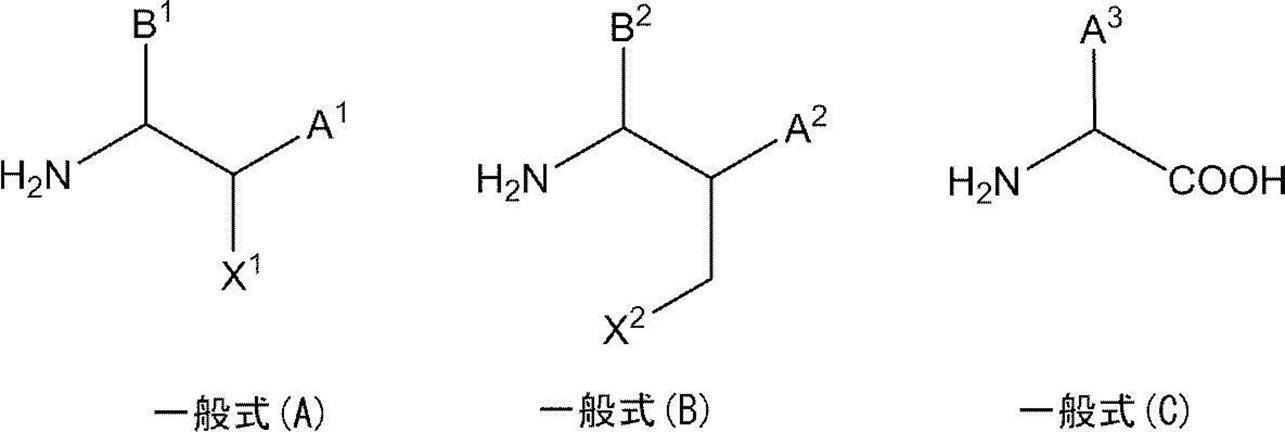
一般式(A)中、X1は、-SH、-NH2、または、-OHを表し、A1及びB1は、各々独立に、水素原子または原子数1以上10以下の置換基を表す。但し、A1及びB1が共に水素原子のときは、X1は-SH、または、-OHを表す。
一般式(B)中、X2は、-SH、-NH2、または、-OHを表し、A2及びB2は、各々独立に、水素原子または原子数1以上10以下の置換基を表す。
一般式(C)中、A3は、水素原子または原子数1以上10以下の置換基を表す。
一般式(B)中、X2は、-SH、-NH2、または、-OHを表し、A2及びB2は、各々独立に、水素原子または原子数1以上10以下の置換基を表す。
一般式(C)中、A3は、水素原子または原子数1以上10以下の置換基を表す。
本発明の半導体膜の製造方法では、半導体量子ドット集合体形成工程および配位子交換工程を繰り返し行ってもよいし、さらに、半導体量子ドット分散液を乾燥する分散液乾燥工程、配位子溶液を乾燥する溶液乾燥工程、基板上の半導体量子ドット集合体を洗浄する洗浄工程等を有していてもよい。
本発明の半導体膜の製造方法では、半導体量子ドット集合体形成工程において、半導体量子ドット分散液を基板上に付与することにより、基板上に半導体量子ドットの集合体を形成する。このとき、半導体量子ドットは、第2の配位子よりも分子鎖長が長い第1の配位子により第1の溶媒に分散されているため、半導体量子ドットは、凝集したバルク状となりにくい。従って、半導体量子ドット分散液が基板上に付与されることで、半導体量子ドットの集合体は、半導体量子ドット1つ1つが配列した構成とすることができる。
次いで、配位子交換工程により、半導体量子ドットの集合体に特定配位子の溶液を付与することで、半導体量子ドットに配位している第1の配位子と、第1の配位子よりも分子鎖長が短い第2の配位子(特定配位子)との配位子交換がなされる。特定配位子は、一般式(A)~(C)に示されるように分子内にアミノ基を有している。既述のように、アミノ基は、錯安定度定数が高く、一般式(A)および(B)においては、半導体量子ドットの金属原子と、X1(またはX2)で表される-SH、-NH2または-OHとの錯体形成を促進すると考えられる。また、一般式(C)においては、アミノ基は、半導体量子ドットの金属原子と、カルボキシ基のOHとの錯体形成を促進すると考えられる。従って、第2の配位子(特定配位子)は、第2の配位子よりも分子鎖長が長い第1の配位子に置き換わって配位し、半導体量子ドットと配位結合を結ぶため、半導体量子ドット同士を近接化し易いと考えられる。半導体量子ドットが近接化することにより、半導体量子ドットの集合体の電気伝導性が高まり、高光電流値を有する半導体膜とすることができると考えられる。
さらに、半導体量子ドット同士が、特定配位子を介して配位結合により結ばれることで、半導体量子ドットの集合体が強固な半導体膜となり、基板上から剥がれ難くなると考えられる。
さらに、半導体量子ドット同士が、特定配位子を介して配位結合により結ばれることで、半導体量子ドットの集合体が強固な半導体膜となり、基板上から剥がれ難くなると考えられる。
〔半導体量子ドット集合体形成工程〕
半導体量子ドット集合体形成工程では、半導体量子ドット、半導体量子ドットに配位した第1の配位子、及び第1の溶媒を含有する半導体量子ドット分散液を基板上に付与して半導体量子ドットの集合体を形成する。
半導体量子ドット分散液は、基板表面に塗布してもよいし、基板上に設けられた他の層に塗布してもよい。
基板上に設けられた他の層としては、基板と半導体量子ドットの集合体との密着を向上させるための接着層、透明導電層等が挙げられる。
半導体量子ドット集合体形成工程では、半導体量子ドット、半導体量子ドットに配位した第1の配位子、及び第1の溶媒を含有する半導体量子ドット分散液を基板上に付与して半導体量子ドットの集合体を形成する。
半導体量子ドット分散液は、基板表面に塗布してもよいし、基板上に設けられた他の層に塗布してもよい。
基板上に設けられた他の層としては、基板と半導体量子ドットの集合体との密着を向上させるための接着層、透明導電層等が挙げられる。
-半導体量子ドット分散液-
半導体量子ドット分散液は、金属原子を有する半導体量子ドット、第1の配位子、および第1の溶媒を含有する。
半導体量子ドット分散液は、本発明の効果を損なわない限度において、更に他の成分を含有していてもよい。
半導体量子ドット分散液は、金属原子を有する半導体量子ドット、第1の配位子、および第1の溶媒を含有する。
半導体量子ドット分散液は、本発明の効果を損なわない限度において、更に他の成分を含有していてもよい。
(半導体量子ドット)
半導体量子ドット分散液が含有する金属原子を含む半導体量子ドットの詳細は既述のとおりであり、好ましい態様も同様である。
なお、半導体量子ドット分散液中の半導体量子ドットの含有量は、1mg/ml~100mg/mlであることが好ましく、5mg/ml~40mg/mlであることがより好ましい。
半導体量子ドット分散液中の半導体量子ドットの含有量が、1mg/ml以上であることで、基板上の半導体量子ドット密度が高くなり、良好な膜が得られ易い。一方、半導体量子ドットの含有量が、100mg/ml以下であることで、半導体量子ドット分散液を一回付与したときに得られる膜の膜厚が大きくなりにくくなる。そのため、膜中の半導体量子ドットに配位する第1の配位子の配位子交換を十分に行うことができる。
半導体量子ドット分散液が含有する金属原子を含む半導体量子ドットの詳細は既述のとおりであり、好ましい態様も同様である。
なお、半導体量子ドット分散液中の半導体量子ドットの含有量は、1mg/ml~100mg/mlであることが好ましく、5mg/ml~40mg/mlであることがより好ましい。
半導体量子ドット分散液中の半導体量子ドットの含有量が、1mg/ml以上であることで、基板上の半導体量子ドット密度が高くなり、良好な膜が得られ易い。一方、半導体量子ドットの含有量が、100mg/ml以下であることで、半導体量子ドット分散液を一回付与したときに得られる膜の膜厚が大きくなりにくくなる。そのため、膜中の半導体量子ドットに配位する第1の配位子の配位子交換を十分に行うことができる。
(第1の配位子)
半導体量子ドット分散液が含有する第1の配位子は、半導体量子ドットに配位する配位子として働くと共に、立体障害となり易い分子構造を有しており、第1の溶媒中に半導体量子ドットを分散させる分散剤としての役割も果たす。
第1の配位子は、後述する第2の配位子よりも分子鎖長が長い。分子鎖長の長短は、分子中に枝分かれ構造がある場合は、主鎖の長さで判断する。第2の配位子である一般式(A)で表される配位子、一般式(B)で表される配位子、および一般式(C)で表される配位子は、そもそも有機溶媒系への分散が困難であり、第1の配位子には該当しない。ここで分散とは、粒子の沈降や濁りがない状態であることを言う。
半導体量子ドット分散液が含有する第1の配位子は、半導体量子ドットに配位する配位子として働くと共に、立体障害となり易い分子構造を有しており、第1の溶媒中に半導体量子ドットを分散させる分散剤としての役割も果たす。
第1の配位子は、後述する第2の配位子よりも分子鎖長が長い。分子鎖長の長短は、分子中に枝分かれ構造がある場合は、主鎖の長さで判断する。第2の配位子である一般式(A)で表される配位子、一般式(B)で表される配位子、および一般式(C)で表される配位子は、そもそも有機溶媒系への分散が困難であり、第1の配位子には該当しない。ここで分散とは、粒子の沈降や濁りがない状態であることを言う。
第1の配位子は、半導体量子ドットの分散を向上する観点から、主鎖の炭素数が少なくとも6以上の配位子であることが望ましく、主鎖の炭素数が10以上の配位子であることがより望ましい。
第1の配位子は、具体的には、飽和化合物でも、不飽和化合物のいずれでもよく、デカン酸、ラウリン酸、ミリスチン酸、パルミチン酸、ステアリン酸、ベヘン酸、オレイン酸、エルカ酸、オレイルアミン、ドデシルアミン、ドデカンチオール、1,2-ヘキサデカンチオール、トリオクチルホスフィンオキシド、臭化セトリモニウム等が挙げられる。
第1の配位子は、半導体膜形成時に、膜中に残存し難いものが好ましい。
第1の配位子は、半導体量子ドットに分散安定性を持たせつつ、半導体膜に残存し難い観点から、以上の中でも、オレイン酸およびオレイルアミンの少なくとも一方が好ましい。
第1の配位子は、具体的には、飽和化合物でも、不飽和化合物のいずれでもよく、デカン酸、ラウリン酸、ミリスチン酸、パルミチン酸、ステアリン酸、ベヘン酸、オレイン酸、エルカ酸、オレイルアミン、ドデシルアミン、ドデカンチオール、1,2-ヘキサデカンチオール、トリオクチルホスフィンオキシド、臭化セトリモニウム等が挙げられる。
第1の配位子は、半導体膜形成時に、膜中に残存し難いものが好ましい。
第1の配位子は、半導体量子ドットに分散安定性を持たせつつ、半導体膜に残存し難い観点から、以上の中でも、オレイン酸およびオレイルアミンの少なくとも一方が好ましい。
半導体量子ドット分散液中の第1の配位子の含有量は、半導体量子ドット分散液の全体積に対し、10mmol/l~200mmol/lであることが望ましい。
(第1の溶媒)
半導体量子ドット分散液が含有する第1の溶媒は、特に制限されないが、半導体量子ドットを溶解し難く、第1の配位子を溶解し易い溶媒であることが好ましい。第1の溶媒は、有機溶剤が好ましく、具体的には、アルカン〔n-ヘキサン、n-オクタン等〕、ベンゼン、トルエン等が挙げられる。
第1の溶媒は、1種のみであってもよいし、2種以上を混合した混合溶媒であってもよい。
半導体量子ドット分散液が含有する第1の溶媒は、特に制限されないが、半導体量子ドットを溶解し難く、第1の配位子を溶解し易い溶媒であることが好ましい。第1の溶媒は、有機溶剤が好ましく、具体的には、アルカン〔n-ヘキサン、n-オクタン等〕、ベンゼン、トルエン等が挙げられる。
第1の溶媒は、1種のみであってもよいし、2種以上を混合した混合溶媒であってもよい。
第1の溶媒は、以上の中でも、形成される半導体膜中に残存し難い溶媒が好ましい。比較的沸点が低い溶媒であれば、最終的に半導体膜を得たときに、残留有機物の含有量を抑えることができる。
さらに、基板への濡れ性が良いものが当然好ましい。たとえば、ガラス基板上へ塗布する場合には、ヘキサン、オクタン等のアルカンがより好ましい。
さらに、基板への濡れ性が良いものが当然好ましい。たとえば、ガラス基板上へ塗布する場合には、ヘキサン、オクタン等のアルカンがより好ましい。
半導体量子ドット分散液中の第1の溶媒の含有量は、半導体量子ドット分散液全質量に対し、90質量%~98質量%であることが好ましい。
-基板-
半導体量子ドット分散液は、基板上に付与される。
基板の形状、構造、大きさ等については特に制限はなく、目的に応じて適宜選択することができる。基板の構造は単層構造であってもよいし、積層構造であってもよい。基板としては、例えば、ガラス、YSZ(Yttria-Stabilized Zirconia;イットリウム安定化ジルコニウム)等の無機材料、樹脂、樹脂複合材料等からなる基板を用いることができる。中でも軽量である点、可撓性を有する点から、樹脂または樹脂複合材料からなる基板が好ましい。
半導体量子ドット分散液は、基板上に付与される。
基板の形状、構造、大きさ等については特に制限はなく、目的に応じて適宜選択することができる。基板の構造は単層構造であってもよいし、積層構造であってもよい。基板としては、例えば、ガラス、YSZ(Yttria-Stabilized Zirconia;イットリウム安定化ジルコニウム)等の無機材料、樹脂、樹脂複合材料等からなる基板を用いることができる。中でも軽量である点、可撓性を有する点から、樹脂または樹脂複合材料からなる基板が好ましい。
樹脂としては、ポリブチレンテレフタレート、ポリエチレンテレフタレート、ポリエチレンナフタレート、ポリブチレンナフタレート、ポリスチレン、ポリカーボネート、ポリスルホン、ポリエーテルスルホン、ポリアリレート、アリルジグリコールカーボネート、ポリアミド、ポリイミド、ポリアミドイミド、ポリエーテルイミド、ポリベンズアゾール、ポリフェニレンサルファイド、ポリシクロオレフィン、ノルボルネン樹脂、ポリクロロトリフルオロエチレン等のフッ素樹脂、液晶ポリマー、アクリル樹脂、エポキシ樹脂、シリコーン樹脂、アイオノマー樹脂、シアネート樹脂、架橋フマル酸ジエステル、環状ポリオレフィン、芳香族エーテル、マレイミドーオレフィン、セルロース、エピスルフィド化合物等の合成樹脂が挙げられる。
無機材料および樹脂の複合材料としては、樹脂と、次の無機材料との複合プラスチック材料が挙げられる。すなわち、樹脂と酸化珪素粒子との複合プラスチック材料、樹脂と金属ナノ粒子との複合プラスチック材料、樹脂と無機酸化物ナノ粒子との複合プラスチック材料、樹脂と無機窒化物ナノ粒子との複合プラスチック材料、樹脂とカーボン繊維との複合プラスチック材料、樹脂とカーボンナノチューブとの複合プラスチック材料、樹脂とガラスフレークとの複合プラスチック材料、樹脂とガラスファイバーとの複合プラスチック材料、樹脂とガラスビーズとの複合プラスチック材料、樹脂と粘土鉱物との複合プラスチック材料、樹脂と雲母派生結晶構造を有する粒子との複合プラスチック材料、樹脂と薄いガラスとの間に少なくとも1つの接合界面を有する積層プラスチック材料、無機層と有機層を交互に積層することで、少なくとも1つ以上の接合界面を有するバリア性能を有する複合材料等が挙げられる。
ステンレス基板またはステンレスと異種金属とを積層した金属多層基板、アルミニウム基板または表面に酸化処理(例えば陽極酸化処理)を施すことで表面の絶縁性を向上させた酸化皮膜付きのアルミニウム基板等を用いてもよい。
なお、樹脂または樹脂複合材料からなる基板(樹脂基板または樹脂複合材料基板)は、耐熱性、寸法安定性、耐溶剤性、電気絶縁性、加工性、低通気性、および低吸湿性等に優れていることが好ましい。樹脂基板および樹脂複合材料基板は、水分、酸素等の透過を防止するためのガスバリア層や、樹脂基板の平坦性や下部電極との密着性を向上するためのアンダーコート層等を備えていてもよい。
また基板上に、下部電極、絶縁膜等を備えていてもよく、その場合には基板上の下部電極や絶縁膜上に半導体量子ドット分散液が付与される。
また基板上に、下部電極、絶縁膜等を備えていてもよく、その場合には基板上の下部電極や絶縁膜上に半導体量子ドット分散液が付与される。
基板の厚みに特に制限はないが、50μm~1000μmが好ましく、50μm~500μmであることがより好ましい。基板の厚みが50μm以上であると、基板自体の平坦性が向上し、基板の厚みが1000μm以下であると、基板自体の可撓性が向上し、半導体膜をフレキシブル半導体デバイスとして使用することがより容易となる。
半導体量子ドット分散液を基板上に付与する手法は、特に限定はなく、半導体量子ドット分散液を基板上に塗布する方法、基板を半導体量子ドット分散液に浸漬する方法等が挙げられる。
半導体量子ドット分散液を基板上に塗布する方法としては、より具体的には、スピンコート法、ディップ法、インクジェット法、ディスペンサー法、スクリーン印刷法、凸版印刷法、凹版印刷法、スプレーコート法等の液相法を用いることができる。
特に、インクジェット法、ディスペンサー法、スクリーン印刷法、凸版印刷法、及び、凹版印刷法は、基板上の任意の位置に塗布膜を形成することができ、且つ、成膜後のパターンニング工程が不要なことから、プロセスコストを低減することができる。
半導体量子ドット分散液を基板上に塗布する方法としては、より具体的には、スピンコート法、ディップ法、インクジェット法、ディスペンサー法、スクリーン印刷法、凸版印刷法、凹版印刷法、スプレーコート法等の液相法を用いることができる。
特に、インクジェット法、ディスペンサー法、スクリーン印刷法、凸版印刷法、及び、凹版印刷法は、基板上の任意の位置に塗布膜を形成することができ、且つ、成膜後のパターンニング工程が不要なことから、プロセスコストを低減することができる。
〔配位子交換工程〕
配位子交換工程では、半導体量子ドット集合体形成工程によって、基板上に形成された半導体量子ドットの集合体に、第1の配位子よりも分子鎖長が短く、かつ、一般式(A)で表される配位子、一般式(B)で表される配位子、および一般式(C)で表される配位子から選択される少なくとも1種である第2の配位子及び第2の溶媒を含有する溶液を付与して、半導体量子ドットに配位する第1の配位子を、配位子溶液に含有される第2の配位子(特定配位子)に交換する。
配位子交換工程では、半導体量子ドット集合体形成工程によって、基板上に形成された半導体量子ドットの集合体に、第1の配位子よりも分子鎖長が短く、かつ、一般式(A)で表される配位子、一般式(B)で表される配位子、および一般式(C)で表される配位子から選択される少なくとも1種である第2の配位子及び第2の溶媒を含有する溶液を付与して、半導体量子ドットに配位する第1の配位子を、配位子溶液に含有される第2の配位子(特定配位子)に交換する。
-配位子溶液-
配位子溶液は、第2の配位子(特定配位子)と、第2の溶媒とを、少なくとも含有する。
配位子溶液は、本発明の効果を損なわない限度において、更に他の成分を含有していてもよい。
配位子溶液は、第2の配位子(特定配位子)と、第2の溶媒とを、少なくとも含有する。
配位子溶液は、本発明の効果を損なわない限度において、更に他の成分を含有していてもよい。
(第2の配位子)
第2の配位子は、既述の特定配位子であり、第1の配位子よりも分子鎖長が短かい。配位子の分子鎖長の長短の判断手法は、第1の配位子の説明において記載したとおりである。
また、特定配位子の詳細も、既述のとおりである。
なお、配位子溶液が含有する第2の溶媒として、アルコールを用いる場合は、特定配位子は分子中にヒドロキシ基(OH)を有することが好ましい。特定配位子が分子構造内にヒドロキシ基を有することで、アルコールとの混和性を高めることができる。また、ヒドロキシ基を有する特定配位子を含有する配位子溶液によって、半導体量子ドットの配位子交換を行う場合は、第2の溶媒としてアルコールを用いると、配位子交換を効率的に行うことができる。
第2の配位子は、既述の特定配位子であり、第1の配位子よりも分子鎖長が短かい。配位子の分子鎖長の長短の判断手法は、第1の配位子の説明において記載したとおりである。
また、特定配位子の詳細も、既述のとおりである。
なお、配位子溶液が含有する第2の溶媒として、アルコールを用いる場合は、特定配位子は分子中にヒドロキシ基(OH)を有することが好ましい。特定配位子が分子構造内にヒドロキシ基を有することで、アルコールとの混和性を高めることができる。また、ヒドロキシ基を有する特定配位子を含有する配位子溶液によって、半導体量子ドットの配位子交換を行う場合は、第2の溶媒としてアルコールを用いると、配位子交換を効率的に行うことができる。
配位子溶液中の特定配位子の含有量は、配位子溶液全体積に対し、5mmol/l~200mmol/lであることが好ましく、10mmol/l~100mmol/lであることがより好ましい。
(第2の溶媒)
配位子溶液が含有する第2の溶媒は、特に制限されないが、特定配位子を溶解し易い溶媒であることが好ましい。
このような溶媒としては、誘電率が高い有機溶媒が好ましく、エタノール、アセトン、メタノール、アセトニトリル、ジメチルホルムアミド、ジメチルスルホキシド、ブタノール、プロパノール等が挙げられる。
第2の溶媒は、1種のみであってもよいし、2種以上を混合した混合溶媒であってもよい。
配位子溶液が含有する第2の溶媒は、特に制限されないが、特定配位子を溶解し易い溶媒であることが好ましい。
このような溶媒としては、誘電率が高い有機溶媒が好ましく、エタノール、アセトン、メタノール、アセトニトリル、ジメチルホルムアミド、ジメチルスルホキシド、ブタノール、プロパノール等が挙げられる。
第2の溶媒は、1種のみであってもよいし、2種以上を混合した混合溶媒であってもよい。
第2の溶媒は、以上の中でも、形成される半導体膜中に残存し難い溶媒が好ましい。乾燥し易く、洗浄により除去し易いとの観点から、低沸点のアルコール、または、アルカンが好ましく、メタノール、エタノール、n-ヘキサン、またはn-オクタンがより好ましい。
また、第2の溶媒は、第1の溶媒とは交じり合わないことが好ましく、例えば、第1の溶媒として、ヘキサン、オクタン等のアルカンを用いた場合は、第2の溶媒は、メタノール、アセトン等の極性溶媒を用いることが好ましい。
なお、配位子溶液中の第2の溶媒の含有量は、配位子溶液全質量から特定配位子の含有量を差し引いた残部である。
また、第2の溶媒は、第1の溶媒とは交じり合わないことが好ましく、例えば、第1の溶媒として、ヘキサン、オクタン等のアルカンを用いた場合は、第2の溶媒は、メタノール、アセトン等の極性溶媒を用いることが好ましい。
なお、配位子溶液中の第2の溶媒の含有量は、配位子溶液全質量から特定配位子の含有量を差し引いた残部である。
配位子溶液を、半導体量子ドットの集合体に付与する方法は、半導体量子ドット分散液を基板上に付与する手法と同様であり、好ましい態様も同様である。
半導体量子ドット集合体形成工程と、配位子交換工程とは、繰り返し行ってもよい。半導体量子ドット集合体形成工程と、配位子交換工程とを繰り返し行うことで、特定配位子が配位した半導体量子ドットの集合体を有する半導体膜の電気伝導度を高め、半導体膜の厚みを厚くすることができる。
半導体量子ドット集合体形成工程、および、配位子交換工程の繰り返しは、それぞれの工程を別途独立に繰り返してもよいが、半導体量子ドット集合体形成工程を行ってから配位子交換工程を行うサイクルを繰り返すことが好ましい。半導体量子ドット集合体形成工程と配位子交換工程とのセットで繰り返すことで、配位子交換のムラを抑制し易くなる。
なお、半導体量子ドット集合体形成工程および配位子交換工程を繰り返して行う場合は、1サイクルごとに十分に膜乾燥を行うことが好ましい。
半導体量子ドット集合体形成工程、および、配位子交換工程の繰り返しは、それぞれの工程を別途独立に繰り返してもよいが、半導体量子ドット集合体形成工程を行ってから配位子交換工程を行うサイクルを繰り返すことが好ましい。半導体量子ドット集合体形成工程と配位子交換工程とのセットで繰り返すことで、配位子交換のムラを抑制し易くなる。
なお、半導体量子ドット集合体形成工程および配位子交換工程を繰り返して行う場合は、1サイクルごとに十分に膜乾燥を行うことが好ましい。
半導体量子ドット集合体の配位子交換における特定配位子への交換率が高いほど、半導体膜の光電流値が大きくなることが期待される。
なお、半導体量子ドットの、第1の配位子と第2の配位子(特定配位子)との配位子交換は、半導体量子ドット集合体の少なくとも一部において行われていれば足り、100%(個数)が特定配位子に取って代わっていなくてもよい。
なお、半導体量子ドットの、第1の配位子と第2の配位子(特定配位子)との配位子交換は、半導体量子ドット集合体の少なくとも一部において行われていれば足り、100%(個数)が特定配位子に取って代わっていなくてもよい。
(洗浄工程)
さらに、本発明の半導体膜の製造方法は、基板上の半導体量子ドット集合体を洗浄する洗浄工程を有していてもよい。
洗浄工程を有することで、過剰な配位子および半導体量子ドットから脱離した配位子を除去することができる。また、残存した溶媒、その他不純物を除去することができる。半導体量子ドット集合体の洗浄は、半導体量子ドットの集合体上に、第1の溶媒および第2の溶媒の少なくとも一方を注いだり、半導体量子ドット集合体または半導体膜が形成された基板を、第1の溶媒および第2の溶媒の少なくとも一方に浸漬すればよい。
洗浄工程による洗浄は、半導体量子ドット集合体形成工程の後に行ってもよいし、配位子交換工程の後に行ってもよい。また、半導体量子ドット集合体形成工程と配位子交換工程とのセットの繰り返しの後に行ってもよい。
さらに、本発明の半導体膜の製造方法は、基板上の半導体量子ドット集合体を洗浄する洗浄工程を有していてもよい。
洗浄工程を有することで、過剰な配位子および半導体量子ドットから脱離した配位子を除去することができる。また、残存した溶媒、その他不純物を除去することができる。半導体量子ドット集合体の洗浄は、半導体量子ドットの集合体上に、第1の溶媒および第2の溶媒の少なくとも一方を注いだり、半導体量子ドット集合体または半導体膜が形成された基板を、第1の溶媒および第2の溶媒の少なくとも一方に浸漬すればよい。
洗浄工程による洗浄は、半導体量子ドット集合体形成工程の後に行ってもよいし、配位子交換工程の後に行ってもよい。また、半導体量子ドット集合体形成工程と配位子交換工程とのセットの繰り返しの後に行ってもよい。
(乾燥工程)
本発明の半導体膜の製造方法は、乾燥工程を有していてもよい。
乾燥工程は、半導体量子ドット集合体形成工程の後に、半導体量子ドット集合体に残存する溶媒を乾燥する分散液乾燥工程であってもよいし、配位子交換工程の後に、配位子溶液を乾燥する溶液乾燥工程であってもよい。また、半導体量子ドット集合体形成工程と配位子交換工程とのセットの繰り返しの後に行う総合的な工程であってもよい。
本発明の半導体膜の製造方法は、乾燥工程を有していてもよい。
乾燥工程は、半導体量子ドット集合体形成工程の後に、半導体量子ドット集合体に残存する溶媒を乾燥する分散液乾燥工程であってもよいし、配位子交換工程の後に、配位子溶液を乾燥する溶液乾燥工程であってもよい。また、半導体量子ドット集合体形成工程と配位子交換工程とのセットの繰り返しの後に行う総合的な工程であってもよい。
以上説明した各工程を経ることによって、基板上に半導体膜が製造される。
得られた半導体膜は、半導体量子ドット同士が従来よりも短い特定配位子で結ばれているため、電気伝導性が高く、高い光電流値が得られる。また、特定配位子は、錯安定度定数が高いため半導体量子ドットと特定配位子とによって構成される本発明の半導体膜は配位結合が安定しており、膜強度にも優れ、膜剥がれも抑制される。
得られた半導体膜は、半導体量子ドット同士が従来よりも短い特定配位子で結ばれているため、電気伝導性が高く、高い光電流値が得られる。また、特定配位子は、錯安定度定数が高いため半導体量子ドットと特定配位子とによって構成される本発明の半導体膜は配位結合が安定しており、膜強度にも優れ、膜剥がれも抑制される。
<電子デバイス>
本発明の半導体膜の用途は限定されないが、本発明の半導体膜は光電変換特性を有し、剥離が生じ難いため、半導体膜又は光電変換膜を有する各種電子デバイスに好適に適用することができる。
具体的には、本発明の半導体膜は、太陽電池の光電変換膜、発光ダイオード(LED)、薄膜トランジスタの半導体層(活性層)、間接型放射線撮像装置の光電変換膜、可視~赤外領域の光検出器等に好適に適用することができる。
本発明の半導体膜の用途は限定されないが、本発明の半導体膜は光電変換特性を有し、剥離が生じ難いため、半導体膜又は光電変換膜を有する各種電子デバイスに好適に適用することができる。
具体的には、本発明の半導体膜は、太陽電池の光電変換膜、発光ダイオード(LED)、薄膜トランジスタの半導体層(活性層)、間接型放射線撮像装置の光電変換膜、可視~赤外領域の光検出器等に好適に適用することができる。
<太陽電池>
本発明の半導体膜、または、本発明の半導体膜の製造方法により製造された半導体膜を備えた電子デバイスの一例として、太陽電池について説明する。
例えば、本発明の半導体膜を含むp型半導体層と、n型半導体層とを備えるpn接合を有する半導体膜デバイスを用いて、pn接合型太陽電池とすることができる。
pn接合型太陽電池のより具体的な実施形態としては、例えば、透明基板上に形成された透明導電膜上にp型半導体層およびn型半導体層が隣接して設けられ、p型半導体層およびn型半導体層の上に金属電極を形成する形態が挙げられる。
本発明の半導体膜、または、本発明の半導体膜の製造方法により製造された半導体膜を備えた電子デバイスの一例として、太陽電池について説明する。
例えば、本発明の半導体膜を含むp型半導体層と、n型半導体層とを備えるpn接合を有する半導体膜デバイスを用いて、pn接合型太陽電池とすることができる。
pn接合型太陽電池のより具体的な実施形態としては、例えば、透明基板上に形成された透明導電膜上にp型半導体層およびn型半導体層が隣接して設けられ、p型半導体層およびn型半導体層の上に金属電極を形成する形態が挙げられる。
pn接合型太陽電池の一例を、図1を用いて説明する。
図1に、本発明の実施形態に係るpn接合型太陽電池100の模式断面図を示す。pn接合型太陽電池100は、透明基板10と、透明基板10上に設けられた透明導電膜12と、透明導電膜12上に本発明の半導体膜で構成されたp型半導体層14と、p型半導体層14上に、n型半導体層16と、n型半導体層16上に設けられた金属電極18とが積層されて構成される。
p型半導体層14とn型半導体層16とが隣接して積層されることで、pn接合型の太陽電池とすることができる。
図1に、本発明の実施形態に係るpn接合型太陽電池100の模式断面図を示す。pn接合型太陽電池100は、透明基板10と、透明基板10上に設けられた透明導電膜12と、透明導電膜12上に本発明の半導体膜で構成されたp型半導体層14と、p型半導体層14上に、n型半導体層16と、n型半導体層16上に設けられた金属電極18とが積層されて構成される。
p型半導体層14とn型半導体層16とが隣接して積層されることで、pn接合型の太陽電池とすることができる。
透明基板10としては、透明であれば、本発明の半導体膜の製造方法で用いる基板と同じ材料を用いることができる。具体的には、ガラス基板、樹脂基板等が挙げられる。本発明では、透明導電膜12としては、In2O3:Sn(ITO)、SnO2:Sb、SnO2:F、ZnO:Al、ZnO:F、CdSnO4等により構成される膜が挙げられる。
p型半導体層14は、既述のように、本発明の半導体膜を用いる。
n型半導体層16としては金属酸化物が好ましい。具体的には、Ti、Zn、Sn、Inの少なくとも一つを含む金属の酸化物が挙げられ、より具体的には、TiO2、ZnO、SnO2、IGZO等が挙げられる。n型半導体層は、製造コストの観点から、p型半導体層と同様に、湿式法(液相法ともいう)で形成されることが好ましい。
金属電極18としては、Pt、Al、Cu、Ti、Ni等を使用することができる。
n型半導体層16としては金属酸化物が好ましい。具体的には、Ti、Zn、Sn、Inの少なくとも一つを含む金属の酸化物が挙げられ、より具体的には、TiO2、ZnO、SnO2、IGZO等が挙げられる。n型半導体層は、製造コストの観点から、p型半導体層と同様に、湿式法(液相法ともいう)で形成されることが好ましい。
金属電極18としては、Pt、Al、Cu、Ti、Ni等を使用することができる。
以下に実施例を説明するが、本発明はこれら実施例により何ら限定されるものではない。
<半導体膜デバイスの作製>
〔半導体量子ドット分散液1の調製〕
まず、PbS粒子をトルエンに分散したPbS粒子分散液を用意した。PbS粒子分散液は、Evident technology社製のPbSコアエヴィドット(公称粒径3.3nm、20mg/ml、溶媒トルエン)を用いた。
次いで、遠沈管に、PbS粒子分散液2mlを取り、38μlのオレイン酸を添加した後、さらに20mlのトルエンを加えて分散液の濃度を薄めた。その後、PbS粒子分散液について超音波分散を行い、PbS粒子分散液をよく攪拌させた。次に、PbS粒子分散液にエタノール40mlを加えて、更に超音波分散を行い、10000rpm、10分、3℃の条件で遠心分離を行った。遠沈管中の上澄みを廃棄した後、遠沈管にオクタンを20ml加えて超音波分散を行い、沈殿した量子ドットをオクタン溶媒によく分散させた。得られた分散物について、ロータリーエバポレーター(35hpa、40℃)を用いて、溶液の濃縮を行い、結果としておよそ10mg/ml濃度の半導体量子ドット分散液1(オクタン溶媒)を4ml程度得た。
半導体量子ドット分散液1に含まれるPbS粒子の平均粒径は3nmであった。
なお、半導体量子ドットの平均粒径は、TEM(Transmission Electron Microscope;透過型電子顕微鏡)測定における写真観察により、半導体量子ドット10個の平均として算出した。測定装置にはFEI社製 TITAN80-300を用いた。
〔半導体量子ドット分散液1の調製〕
まず、PbS粒子をトルエンに分散したPbS粒子分散液を用意した。PbS粒子分散液は、Evident technology社製のPbSコアエヴィドット(公称粒径3.3nm、20mg/ml、溶媒トルエン)を用いた。
次いで、遠沈管に、PbS粒子分散液2mlを取り、38μlのオレイン酸を添加した後、さらに20mlのトルエンを加えて分散液の濃度を薄めた。その後、PbS粒子分散液について超音波分散を行い、PbS粒子分散液をよく攪拌させた。次に、PbS粒子分散液にエタノール40mlを加えて、更に超音波分散を行い、10000rpm、10分、3℃の条件で遠心分離を行った。遠沈管中の上澄みを廃棄した後、遠沈管にオクタンを20ml加えて超音波分散を行い、沈殿した量子ドットをオクタン溶媒によく分散させた。得られた分散物について、ロータリーエバポレーター(35hpa、40℃)を用いて、溶液の濃縮を行い、結果としておよそ10mg/ml濃度の半導体量子ドット分散液1(オクタン溶媒)を4ml程度得た。
半導体量子ドット分散液1に含まれるPbS粒子の平均粒径は3nmであった。
なお、半導体量子ドットの平均粒径は、TEM(Transmission Electron Microscope;透過型電子顕微鏡)測定における写真観察により、半導体量子ドット10個の平均として算出した。測定装置にはFEI社製 TITAN80-300を用いた。
〔半導体量子ドット分散液2の調製〕
まず、InP粒子を合成し、オレイルアミンが配位したInP粒子のオクタン分散液を調製した。
まず、InP粒子を合成し、オレイルアミンが配位したInP粒子のオクタン分散液を調製した。
-オレイルアミン修飾InP粒子のオクタン分散液の調製-
グローブボックス中、N2ガス雰囲気下で、三つ口丸底フラスコに、1-オクタデセン30ml、オレイルアミン1.81ml、無水塩化インジウム0.60g、トリスジメチルアミノホスフィン0.49ml、およびマグネット撹拌子を入れた。次いで、三つ口丸底フラスコを三方弁付きの栓で密閉した状態でグローブボックスから取り出し、マグネットスターラー付きアルミブロック恒温槽にセットした。その後、三方弁を操作してフラスコ内にN2ガスを通気し、マグネット撹拌子で混合物を激しく撹拌しながら、アルミブロック恒温槽の加熱を開始した。アルミブロック恒温槽の温度は、約30分で150℃まで昇温し、そのまま5時間保持した。その後、加熱を停止して、三つ口丸底フラスコを、送風ファンを用いて室温まで冷却した。
グローブボックス中、N2ガス雰囲気下で、三つ口丸底フラスコに、1-オクタデセン30ml、オレイルアミン1.81ml、無水塩化インジウム0.60g、トリスジメチルアミノホスフィン0.49ml、およびマグネット撹拌子を入れた。次いで、三つ口丸底フラスコを三方弁付きの栓で密閉した状態でグローブボックスから取り出し、マグネットスターラー付きアルミブロック恒温槽にセットした。その後、三方弁を操作してフラスコ内にN2ガスを通気し、マグネット撹拌子で混合物を激しく撹拌しながら、アルミブロック恒温槽の加熱を開始した。アルミブロック恒温槽の温度は、約30分で150℃まで昇温し、そのまま5時間保持した。その後、加熱を停止して、三つ口丸底フラスコを、送風ファンを用いて室温まで冷却した。
三つ口丸底フラスコ内から生成物を取り出し、遠心分離機を用いた遠心分離により未反応物と副生成物を除去した。良溶媒として超脱水トルエンを用い、貧溶媒として脱水エタノールを用いて、生成物(InP粒子)を精製した。具体的には、生成物を良溶媒に溶解し、InP粒子溶解物を貧溶媒に再分散し、得られたInP粒子分散液を遠心分離する処理を繰り返した。なお、再分散には超音波洗浄機を用いた。InP粒子分散液の遠心分離を繰り返した後、InP粒子分散液中に残った脱水エタノールは、ロータリーエバポレーターを用いて減圧蒸留して取り除いた。最後にオクタンに、抽出したInP粒子を分散させて、オレイルアミン修飾InP粒子濃度が1mg/mlのオクタン分散液を得た。これを半導体量子ドット分散液2とした。
得られたInP粒子をTEM観察したところ、平均粒径が約4nmの粒子であった。
得られたInP粒子をTEM観察したところ、平均粒径が約4nmの粒子であった。
〔半導体量子ドット分散液3の調製〕
三口フラスコ中に、1-オクタデセン30ml、酸化鉛(II)6.32mmol、および、オレイン酸21.2mmolを、それぞれ計量して混合した。混合物は、アルミブロックホットプレートスターラーを用いて、300rpmにてマグネット攪拌子で攪拌した。混合物の撹拌中、120℃で1時間、真空引きしながら脱気と脱水を行った。次に、冷却ファンを用いて、三口フラスコを室温まで冷却し、窒素ガスによる通気を行ってから、ヘキサメチルジシラチアン2.57mmolと1-オクタデセン5mlを含む溶液をシリンジで三口フラスコ内に注入した(セプタムキャップをシリンジ針で刺して注入)。その後、40分間かけて120℃まで三口フラスコを加熱し、1分間保持した後に、三口フラスコを冷却ファンで室温まで冷却した。遠心分離機を用いて、得られた生成物から不要物を除去し、PbS粒子のみを抽出し、オクタンに分散した。なお、生成物から不要物を除去する際には、良溶媒にトルエンを用い、貧溶媒に脱水エタノールを用いた。
STEM(Scanning Transmission Electron Microscope;走査透過型電子顕微鏡)による観察の結果、得られたPbSの平均粒径は5nmであることがわかった。
更にこのPbS量子ドットのオクタン分散液をヘキサン溶媒で希釈することで、およそ10mg/ml濃度の半導体量子ドット分散液3〔オクタン:ヘキサン=1:9(体積比)の混合溶媒〕を得た。
三口フラスコ中に、1-オクタデセン30ml、酸化鉛(II)6.32mmol、および、オレイン酸21.2mmolを、それぞれ計量して混合した。混合物は、アルミブロックホットプレートスターラーを用いて、300rpmにてマグネット攪拌子で攪拌した。混合物の撹拌中、120℃で1時間、真空引きしながら脱気と脱水を行った。次に、冷却ファンを用いて、三口フラスコを室温まで冷却し、窒素ガスによる通気を行ってから、ヘキサメチルジシラチアン2.57mmolと1-オクタデセン5mlを含む溶液をシリンジで三口フラスコ内に注入した(セプタムキャップをシリンジ針で刺して注入)。その後、40分間かけて120℃まで三口フラスコを加熱し、1分間保持した後に、三口フラスコを冷却ファンで室温まで冷却した。遠心分離機を用いて、得られた生成物から不要物を除去し、PbS粒子のみを抽出し、オクタンに分散した。なお、生成物から不要物を除去する際には、良溶媒にトルエンを用い、貧溶媒に脱水エタノールを用いた。
STEM(Scanning Transmission Electron Microscope;走査透過型電子顕微鏡)による観察の結果、得られたPbSの平均粒径は5nmであることがわかった。
更にこのPbS量子ドットのオクタン分散液をヘキサン溶媒で希釈することで、およそ10mg/ml濃度の半導体量子ドット分散液3〔オクタン:ヘキサン=1:9(体積比)の混合溶媒〕を得た。
〔配位子溶液の調製〕
表1の「配位子」欄の「化合物名」欄に示す配位子を1mmol取り分け、10mlのメタノールに溶かし、0.1mol/l濃度の配位子溶液を調製した。配位子溶液中の配位子の溶解を促進するため、超音波照射し、可能な限り配位子の溶け残りがないようにした。
表1の「配位子」欄の「化合物名」欄に示す配位子を1mmol取り分け、10mlのメタノールに溶かし、0.1mol/l濃度の配位子溶液を調製した。配位子溶液中の配位子の溶解を促進するため、超音波照射し、可能な限り配位子の溶け残りがないようにした。
〔基板〕
基板は、石英ガラス上に、図2に示す65対のくし型白金電極を有する基板を準備した。くし型白金電極は、BAS社製のくし型電極(型番012126、電極間隔5μm)を用いた。
基板は、石英ガラス上に、図2に示す65対のくし型白金電極を有する基板を準備した。くし型白金電極は、BAS社製のくし型電極(型番012126、電極間隔5μm)を用いた。
〔半導体膜の製造〕
(1)半導体量子ドット集合体形成工程
調製した半導体量子ドット分散液1または半導体量子ドット分散液2を基板に滴下後、2500rpmでスピンコートし、半導体量子ドット集合体膜を得た。
(1)半導体量子ドット集合体形成工程
調製した半導体量子ドット分散液1または半導体量子ドット分散液2を基板に滴下後、2500rpmでスピンコートし、半導体量子ドット集合体膜を得た。
(2)配位子交換工程
さらに、半導体量子ドット集合体膜の上に、表1に示す配位子のメタノール溶液(配位子溶液)を滴下した後、2500rpmでスピンコートし、半導体膜を得た。
さらに、半導体量子ドット集合体膜の上に、表1に示す配位子のメタノール溶液(配位子溶液)を滴下した後、2500rpmでスピンコートし、半導体膜を得た。
(3)洗浄工程1
次いで、配位子溶液の溶媒であるメタノールだけを半導体膜上に滴下し、スピンコートした。
次いで、配位子溶液の溶媒であるメタノールだけを半導体膜上に滴下し、スピンコートした。
(4)洗浄工程2
さらに、洗浄工程1による洗浄後の半導体膜に、オクタン溶媒だけを滴下し、スピンコートした。
さらに、洗浄工程1による洗浄後の半導体膜に、オクタン溶媒だけを滴下し、スピンコートした。
(1)~(4)の一連の工程を15サイクル繰り返すことで、PbS量子ドットの集合体からなり、配位子交換が施された厚み100nmの半導体膜を得た。
以上のようにして、基板上に半導体膜を有する半導体膜デバイスを作製した。
以上のようにして、基板上に半導体膜を有する半導体膜デバイスを作製した。
実施例および比較例における、半導体量子ドット分散液と、配位子溶液との組み合わせは、表1に示すとおりである。表1において、「半導体量子ドット」欄の「種」欄の「PbS」は、半導体量子ドット分散液1を用いたことを意味し、「InP」は、半導体量子ドット分散液2を用いたことを意味する。
また、配位子溶液に含まれる配位子の種類は、表1の「配位子」欄の「化合物名」欄に示す配位子である。
また、配位子溶液に含まれる配位子の種類は、表1の「配位子」欄の「化合物名」欄に示す配位子である。
なお、「配位子」「一般式」「種」欄の「A」は、配位子が一般式(A)で表されることを意味し、「B」は、配位子が一般式(B)で表されることを意味し、「C」は、配位子が一般式(C)で表されることを意味する。一般式(A)、(B)および(C)で表せない配位子は「-」とした。また、「A数」は、A1、A2またはA3の原子数を表し、「B数」は、B1またはB2の原子数を表す。
また、比較例4で用いている配位子は、臭化カリウム(KBr)であり、比較例5で用いている配位子は、セチルトリメチルアンモニウムブロマイド〔(CH3(CH2)15N(CH3)3)+、Br-〕である。
また、比較例4で用いている配位子は、臭化カリウム(KBr)であり、比較例5で用いている配位子は、セチルトリメチルアンモニウムブロマイド〔(CH3(CH2)15N(CH3)3)+、Br-〕である。
<半導体膜の評価>
得られた半導体膜デバイスの半導体膜について、種々の評価を行った。
得られた半導体膜デバイスの半導体膜について、種々の評価を行った。
1.電気伝導性
作製した半導体膜デバイスについて半導体パラメータアナライザーを用いることで、半導体膜の電気伝導性の評価を行った。
まず、半導体膜デバイスに光を照射しない状態で電極への印加電圧を-5~5Vの間で掃引し、暗状態でのI-V特性を取得した。+5Vのバイアスを印加した状態での電流値を暗電流の値Idとして採用した。
次に、半導体膜デバイスにモノクロ光(照射強度1013フォトン)を照射した状態での光電流値を評価した。なお、半導体膜デバイスへのモノクロ光の照射は、図3に示す装置を用いて行った。モノクロ光の波長は280nm~700nmの間で系統的に変化させた。280nmの波長の光を照射した場合の暗電流からの電流の増加分を光電流値Ipとした。
評価結果を、表1に示す。
作製した半導体膜デバイスについて半導体パラメータアナライザーを用いることで、半導体膜の電気伝導性の評価を行った。
まず、半導体膜デバイスに光を照射しない状態で電極への印加電圧を-5~5Vの間で掃引し、暗状態でのI-V特性を取得した。+5Vのバイアスを印加した状態での電流値を暗電流の値Idとして採用した。
次に、半導体膜デバイスにモノクロ光(照射強度1013フォトン)を照射した状態での光電流値を評価した。なお、半導体膜デバイスへのモノクロ光の照射は、図3に示す装置を用いて行った。モノクロ光の波長は280nm~700nmの間で系統的に変化させた。280nmの波長の光を照射した場合の暗電流からの電流の増加分を光電流値Ipとした。
評価結果を、表1に示す。
2.基板からの膜剥がれ
実施例および比較例の半導体膜デバイスについて、目視により、半導体膜の膜剥がれを評価した。膜剥がれの有無を表1に示す。
実施例および比較例の半導体膜デバイスについて、目視により、半導体膜の膜剥がれを評価した。膜剥がれの有無を表1に示す。
3.錯安定度(logβ1)
実施例および比較例の半導体膜が有する配位子の錯安定度定数(logβ1)は、Sc-Database ver.5.85 (Academic Software)(2010)を検索して得た。
また、Sc-Databaseに挙げられていない配位子の錯安定度定数(logβ1)は、半導体量子ドット分散液中の半導体量子ドット(PbS粒子またはInP粒子)の濃度と、配位子溶液中の配位子の濃度とから、既述の式(b)を用い、算出した。
結果を、表1に示す。
なお、Sc-Database ver.5.85に記載されておらず、算出することが困難であったものは、「-」と示した。
実施例および比較例の半導体膜が有する配位子の錯安定度定数(logβ1)は、Sc-Database ver.5.85 (Academic Software)(2010)を検索して得た。
また、Sc-Databaseに挙げられていない配位子の錯安定度定数(logβ1)は、半導体量子ドット分散液中の半導体量子ドット(PbS粒子またはInP粒子)の濃度と、配位子溶液中の配位子の濃度とから、既述の式(b)を用い、算出した。
結果を、表1に示す。
なお、Sc-Database ver.5.85に記載されておらず、算出することが困難であったものは、「-」と示した。

表1に示されるように、半導体量子ドットに配位するオレイン酸配位子を配位子交換して、一般式(A)、一般式(B)または一般式(C)で表される配位子で半導体量子ドットを結ぶことで、従来のエタンジチオールが配位した半導体膜(比較例1)に対して、高い光電流値および暗電流値が得られることが分かった。
また、エタンジチオールが配位した半導体膜については、肉眼で顕著な膜剥がれが生じているのに対し、実施例の半導体膜デバイスは膜剥がれが認められず、良好なラフネスが実現された。
さらに、配位子としてエチレンジアミンを用いた半導体膜(比較例2)では、光電流値、暗電流値、ともに著しく低くなることが分かった。
また、エタンジチオールが配位した半導体膜については、肉眼で顕著な膜剥がれが生じているのに対し、実施例の半導体膜デバイスは膜剥がれが認められず、良好なラフネスが実現された。
さらに、配位子としてエチレンジアミンを用いた半導体膜(比較例2)では、光電流値、暗電流値、ともに著しく低くなることが分かった。
以上より、表1に示される結果は、配位子として、単純な1級アミンまたはジアミンを用いた場合には、良好な電気伝導特性が得られないことを示唆している。これは、単純な1級アミンまたはジアミンは、logβ1があまり高くなく、配位子の配位があまり進行していないことが可能性として考えられる。そのため、オレイン酸が配位子として残り、半導体量子ドット間のキャリアの輸送を阻害していると思われる。
また、特にキャリア輸送特性が高い、実施例1~実施例3の結果から、一般式(A)におけるX1、および、一般式(B)におけるX2が、OHまたはSHであると、高い光電流値が得られ、電気伝導特性に優れることが分かる。
また、特にキャリア輸送特性が高い、実施例1~実施例3の結果から、一般式(A)におけるX1、および、一般式(B)におけるX2が、OHまたはSHであると、高い光電流値が得られ、電気伝導特性に優れることが分かる。
このように半導体量子ドットに、特定配位子を配位させた半導体膜を作製することによって、高い光電流と高い電気伝導性が実現できると共に膜剥がれが抑制されることが示された。
4.光電流値の照射エネルギー依存性
「1.電気伝導性]評価で行った光電流値評価において、照射フォトン数を一定にし、照射エネルギーを変化させたときの、光電流値の照射エネルギー依存性について評価した。評価結果を、図4に示す。
「1.電気伝導性]評価で行った光電流値評価において、照射フォトン数を一定にし、照射エネルギーを変化させたときの、光電流値の照射エネルギー依存性について評価した。評価結果を、図4に示す。
5.半導体量子ドットにおける発光スペクトル
表1に示される実施例および比較例の評価結果からわかるように、特定配位子を用いて半導体量子ドット同士を近接化することで、半導体膜の電気伝導性を向上することができる。しかし、その一方で、半導体量子ドット同士が近接化し過ぎると、半導体量子ドットの凝集化を生じ易い。半導体量子ドットは、凝集することでバルクのような性質になってしまうことが予想される。
半導体膜は、良好な電気特性を示しながらも、半導体量子ドットとしての物性を保持していることが望ましい。特に、半導体膜をLEDまたは太陽電池に応用することを考えた場合には、半導体膜が、半導体量子ドットとしての物性を有していなければ、目的とする波長の吸収や発光を得にくくなる。
表1に示される実施例および比較例の評価結果からわかるように、特定配位子を用いて半導体量子ドット同士を近接化することで、半導体膜の電気伝導性を向上することができる。しかし、その一方で、半導体量子ドット同士が近接化し過ぎると、半導体量子ドットの凝集化を生じ易い。半導体量子ドットは、凝集することでバルクのような性質になってしまうことが予想される。
半導体膜は、良好な電気特性を示しながらも、半導体量子ドットとしての物性を保持していることが望ましい。特に、半導体膜をLEDまたは太陽電池に応用することを考えた場合には、半導体膜が、半導体量子ドットとしての物性を有していなければ、目的とする波長の吸収や発光を得にくくなる。
このことは、配位子を有する半導体量子ドットにおけるPL(Photo Luminescence)スペクトルのピーク波長から判断することができる。
そこで、実施例のうち実施例1および2、比較例のうち、比較例1、比較例4~8における半導体膜のPLスペクトル測定を行った。また、参考のため、配位子としてグリコール酸を用いたPbS半導体量子ドットの膜(比較例11)、配位子交換をせずにオレイン酸が配位したままのPbS半導体量子ドットの膜(比較例12)、およびPbSバルク(比較例13)のPLスペクトルも測定した。
そこで、実施例のうち実施例1および2、比較例のうち、比較例1、比較例4~8における半導体膜のPLスペクトル測定を行った。また、参考のため、配位子としてグリコール酸を用いたPbS半導体量子ドットの膜(比較例11)、配位子交換をせずにオレイン酸が配位したままのPbS半導体量子ドットの膜(比較例12)、およびPbSバルク(比較例13)のPLスペクトルも測定した。
ここで、比較例11の膜は、実施例1において、配位子をグリコール酸に変更したほかは同様にして得た配位子溶液を用いて、実施例1と同様にして得た半導体膜である。比較例12の膜は、実施例1において、「半導体膜の製造」における(1)~(4)の工程のうち、(2)および(3)の工程を行わずにして得た膜である。なお、比較例12の膜は、半導体量子ドット同士が近接化していないため、電気伝導性を示さない絶縁膜であった。
また、PbSバルクは、一般的なII-VI族半導体でありPbSの単結晶であり、サイズが100nmよりも大きく、量子サイズ効果が生じていない半導体である。
また、PbSバルクは、一般的なII-VI族半導体でありPbSの単結晶であり、サイズが100nmよりも大きく、量子サイズ効果が生じていない半導体である。
フォトルミネッセンス測定に用いた実験系のセットアップの構成を図5に概略的に示す。この実験装置は、主に、レーザ照射器20、全反射ミラー22、ダイクロイックミラー24、レンズ26,28、分光器32を備え、レーザ照射器20から発せられたレーザ光が、全反射ミラー22、ダイクロイックミラー24、レンズ26および28を経て、それぞれ測定サンプル(評価用デバイスの半導体膜)30と分光器32に到達する構成を有している。
図6~図8にPLスペクトルを示す。なお、図6には、実施例1(曲線A)、実施例2(曲線B)、および比較例12(曲線C)のPLスペクトルを示した。図7には、比較例1(曲線D)、および比較例12(曲線C)のPLスペクトルを示し、図8には、比較例4~8のPLスペクトル(曲線E~曲線I)を示す。
また、各配位子におけるピーク波長を表2にまとめた。
図6~図8にPLスペクトルを示す。なお、図6には、実施例1(曲線A)、実施例2(曲線B)、および比較例12(曲線C)のPLスペクトルを示した。図7には、比較例1(曲線D)、および比較例12(曲線C)のPLスペクトルを示し、図8には、比較例4~8のPLスペクトル(曲線E~曲線I)を示す。
また、各配位子におけるピーク波長を表2にまとめた。

図6~図8、及び表2からわかるように、配位子交換をせずにオレイン酸が配位したままのPbS半導体量子ドット(比較例12)については、ピーク波長が1100nm程度であった。それに対し、2-アミノエタン-1-チオールが配位した半導体膜(実施例1)を除く半導体膜では、60nm~120nm程度、ピーク波長が長波側にシフトしていることが分かる。
ピーク波長の長波長側へのシフトは、配位子交換により、半導体量子ドット同士が近接化したことによって、半導体量子ドットの閉じ込めポテンシャルが減少し、実効的にバンドギャップが低下しているためである。バンドギャップの低下分は、最も大きいもので、およそ100meV程度である。
ピーク波長の長波長側へのシフトは、配位子交換により、半導体量子ドット同士が近接化したことによって、半導体量子ドットの閉じ込めポテンシャルが減少し、実効的にバンドギャップが低下しているためである。バンドギャップの低下分は、最も大きいもので、およそ100meV程度である。
一方、PbSバルク(比較例13)の場合、バンドギャップがおよそ0.37eV程度であることから、発光ピークは3350nm程度に存在する。従って、仮に、半導体膜の半導体量子ドットが凝集体となっていれば、半導体量子ドットの凝集体で構成された半導体膜の発光ピークは、3350nm近辺に現れると考えられる。
これに対し、実施例1および実施例2に示すように、特定配位子で配位された半導体量子ドットの半導体膜は、半導体量子ドット間隔が短くなり、半導体量子ドットを介した高い電気伝導特性を示す一方で、半導体量子ドットとしての物性(バンドギャップ等)を保持していることが確認された。
また、2-アミノエタンチオールで配位された半導体量子ドットの半導体膜(実施例1)に関しては、ピーク波長が1290nm近辺に現れることが分かった。
実施例1の半導体膜の発光ピークは、バルクの発光ピークとも通常の半導体量子ドットの発光ピークとも異なっており、半導体量子ドット同士が極めて近接化することで、半導体量子ドットのエネルギー準位が変調された新たなエネルギー準位の形成を示唆する結果である。
実施例1の半導体膜の発光ピークは、バルクの発光ピークとも通常の半導体量子ドットの発光ピークとも異なっており、半導体量子ドット同士が極めて近接化することで、半導体量子ドットのエネルギー準位が変調された新たなエネルギー準位の形成を示唆する結果である。
6.半導体量子ドットの平均粒径
半導体量子ドットの平均粒径を、TEM装置により測定した。測定装置には、FEI社製のTITAN80-300を用いた。試料は2種用意した。1つは、半導体量子ドット分散液1を、Si基板上にドロップキャストしたものを、サンプリングナイフで採取して、測定ステージに乗せたものである。もう1つは、エタンジチオールで配位子交換を行ったスピンコート膜を石英ガラス基板上に形成し、同様にサンプリングナイフで採取したものである。後者の試料は、つまり、比較例1の半導体膜の作製において、基板として石英ガラス基板を用いたほかは同様にして得た半導体膜である。
半導体量子ドットの平均粒径を、TEM装置により測定した。測定装置には、FEI社製のTITAN80-300を用いた。試料は2種用意した。1つは、半導体量子ドット分散液1を、Si基板上にドロップキャストしたものを、サンプリングナイフで採取して、測定ステージに乗せたものである。もう1つは、エタンジチオールで配位子交換を行ったスピンコート膜を石英ガラス基板上に形成し、同様にサンプリングナイフで採取したものである。後者の試料は、つまり、比較例1の半導体膜の作製において、基板として石英ガラス基板を用いたほかは同様にして得た半導体膜である。
図9に、半導体量子ドット分散液1をドロップキャストした場合のTEM画像を示す。図9から量子ドットの平均粒径(10個平均)が3nmであることが確認された。また、配位子交換をせずに、長鎖脂肪酸であるオレイン酸が配位したままとなっているために、半導体量子ドットの間隔が非常に広い(2nm~4nm)ことが分かる。
一方、配位子交換を行ったスピンコート膜のTEM画像を図10に示す。Ip/Idがあまり高くないエタンジチオールが配位している半導体膜ではあるものの、半導体量子ドット間の間隔が狭まり、半導体量子ドット同士が密集するような構造を示していることが分かる。従って、半導体量子ドットに特定配位子が配位した本発明の半導体膜における電気伝導性向上の主要因は、半導体量子ドット同士の近接化であることが確認された。
7.半導体膜中の半導体量子ドットのドット間平均最短距離
まず、次のようにして、実施例12、実施例13、比較例14、および比較例15の各量子ドット膜(試料)を作製した。
まず、次のようにして、実施例12、実施例13、比較例14、および比較例15の各量子ドット膜(試料)を作製した。
〔半導体膜の製造〕
まず、石英ガラス上にヘキサメチルジシラザン溶液をスピンコートし、表面の疎水化を行った。その上で以下の様な手順で半導体量子ドットの集合体を有する半導体膜を用意した。
(I)半導体量子ドット集合体形成工程
調製した半導体量子ドット分散液3をドロップキャストし、半導体量子ドット集合体膜を得た。
まず、石英ガラス上にヘキサメチルジシラザン溶液をスピンコートし、表面の疎水化を行った。その上で以下の様な手順で半導体量子ドットの集合体を有する半導体膜を用意した。
(I)半導体量子ドット集合体形成工程
調製した半導体量子ドット分散液3をドロップキャストし、半導体量子ドット集合体膜を得た。
(II)配位子交換工程
さらに、半導体量子ドット集合体膜を、表3に示す配位子のメタノール溶液中に3分間浸漬し、第1の配位子であるオレイン酸から、表3に示す配位子への交換処理を実行した。このようにして、実施例および比較例の量子ドット膜を得た。
さらに、半導体量子ドット集合体膜を、表3に示す配位子のメタノール溶液中に3分間浸漬し、第1の配位子であるオレイン酸から、表3に示す配位子への交換処理を実行した。このようにして、実施例および比較例の量子ドット膜を得た。
(III)洗浄工程i
次いで、各量子ドット膜を、メタノール溶媒中に浸漬した。
次いで、各量子ドット膜を、メタノール溶媒中に浸漬した。
(IV)洗浄工程ii
さらに、洗浄工程iによる洗浄後の量子ドット膜を、オクタン溶媒中に浸漬した。
さらに、洗浄工程iによる洗浄後の量子ドット膜を、オクタン溶媒中に浸漬した。
(I)~(IV)の一連の工程を2サイクル繰り返すことで、PbS量子ドットの集合体からなり、配位子交換が施された厚み20nmの半導体膜を得た。
なお、比較例15については、(I)半導体量子ドット集合体形成工程が完了した時点での半導体量子ドット集合体膜を用いた。
なお、比較例15については、(I)半導体量子ドット集合体形成工程が完了した時点での半導体量子ドット集合体膜を用いた。
得られた実施例12、実施例13、比較例14、および比較例15の量子ドット膜(試料)について、微小角入射X線小角散乱法(GISAXS)によって構造評価を行った。入射光はCuのKα線とし、全反射角よりもわずかに大きい入射角(およそ0.4°程度)で、量子ドット膜にX線を照射し、検出器を面内方向にスキャンすることで散乱光の検出を行った。
実施例12、実施例13、及び比較例14の半導体膜について、それぞれの配位子種に対する散乱光のバックグラウンド構造を差し引いた散乱光の面内角度依存性を図11に示す。
実施例12、実施例13、及び比較例14の半導体膜について、それぞれの配位子種に対する散乱光のバックグラウンド構造を差し引いた散乱光の面内角度依存性を図11に示す。
実施例12、実施例13、及び比較例14の試料については図11に示すように、また、比較例15については図示しないが、いずれの試料においても面内の周期構造を反映した散乱ピークが得られた。ここで得られた散乱ピーク位置をθMAXとすると、試料における半導体量子ドット間の中心間距離dは以下の式(D)で算出される。
d=λ/2sinθMAX・・・(D)
d=λ/2sinθMAX・・・(D)
式(D)中、λは入射光の波長である。
上記散乱ピークから算出した隣接する量子ドット間の距離(測定された量子ドット間の中心間距離dから、量子ドットの粒子径を差し引いたもの)のうち、最短のものを表3に示した。なお、検出された散乱光は、測定装置においてX線が照射された全ての領域に存在する試料についての散乱X線の平均である。
上記散乱ピークから算出した隣接する量子ドット間の距離(測定された量子ドット間の中心間距離dから、量子ドットの粒子径を差し引いたもの)のうち、最短のものを表3に示した。なお、検出された散乱光は、測定装置においてX線が照射された全ての領域に存在する試料についての散乱X線の平均である。
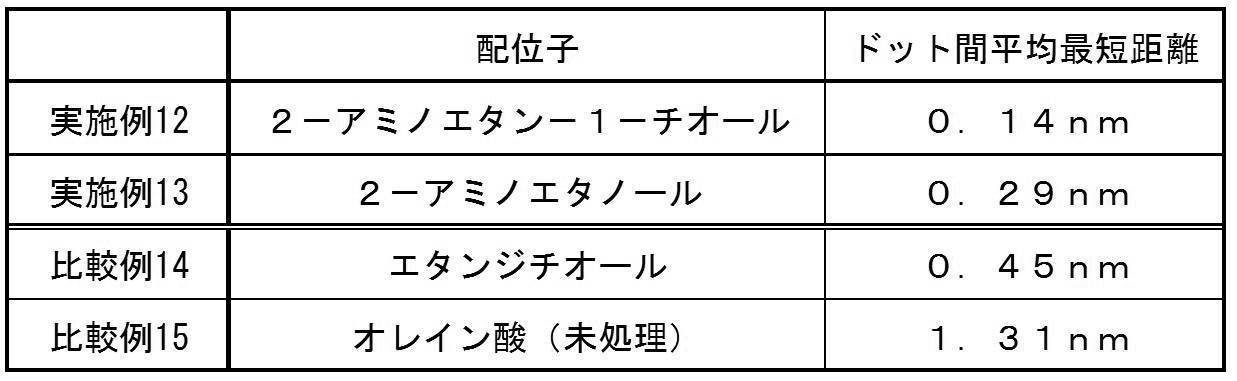
表3より、初期配位子(第1の配位子)であるオレイン酸に対して、配位子交換処理を行った膜(実施例12、実施例13、及び比較例14)では、いずれも量子ドット間隔(量子ドット間距離)が減少していることが分かる。特に、一般式(A)で表される特定配位子の2-アミノエタン-1-チオールや2-アミノエタノールでは、半導体量子ドット間の近接度が、従来のエタンジチオール配位膜と比較して、さらに高いことが確認された。
この半導体量子ドット間の近接化の結果と、表1に示される電気伝導測定の結果より、従来のエタンジチオールが配位した半導体膜よりもドット間平均最短距離が小さいもの(0.45nm未満)に関しては、高い光電流値および高い暗電流値が得られることが分かった。また、エタンジチオールが配位した半導体膜については、肉眼で顕著な膜剥がれが生じているのに対し、実施例の特定配位子が配位した半導体膜については、膜剥がれが認められず良好なラフネスが実現された。
上記に示す結果から、基本的にはドット間平均最短距離が小さい量子ドット半導体膜の方が、高い電気伝導性を実現可能であることがわかった。半導体量子ドットへの配位子の配位形態に依らず、確実に高い電気伝導性を得るためには、ドット間平均最短距離は0.3nm未満であることが望ましく、更に望ましくは2-アミノエタン-1-チオール配位の場合のように、ドット間平均最短距離が0.2nm未満であることが望ましいことが分かった。
日本国特許出願2012-241230号および2012-282431号の開示はその全体が参照により本明細書に取り込まれる。
本明細書に記載された全ての文献、特許出願、および技術規格は、個々の文献、特許出願、および技術規格が参照により取り込まれることが具体的かつ個々に記された場合と同程度に、本明細書中に参照により取り込まれる。
本明細書に記載された全ての文献、特許出願、および技術規格は、個々の文献、特許出願、および技術規格が参照により取り込まれることが具体的かつ個々に記された場合と同程度に、本明細書中に参照により取り込まれる。
Claims (26)
- 金属原子を含む半導体量子ドットの集合体と、
前記半導体量子ドットに配位し、下記一般式(A)で表される配位子、下記一般式(B)で表される配位子、および下記一般式(C)で表される配位子からなる群から選択される少なくとも1種の配位子と、
を有する半導体膜。
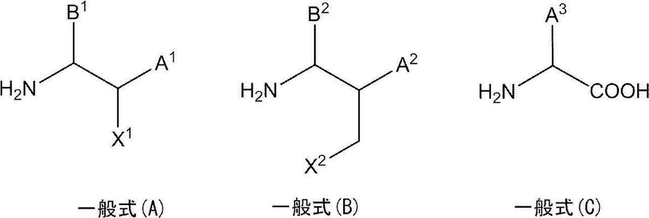
〔一般式(A)中、X1は、-SH、-NH2、または、-OHを表し、A1及びB1は、各々独立に、水素原子または原子数1以上10以下の置換基を表す。但し、A1及びB1が共に水素原子のときは、X1は-SH、または、-OHを表す。
一般式(B)中、X2は、-SH、-NH2、または、-OHを表し、A2及びB2は、各々独立に、水素原子または原子数1以上10以下の置換基を表す。
一般式(C)中、A3は、水素原子または原子数1以上10以下の置換基を表す。〕 - 前記A1、前記B1、前記A2、前記B2、及び前記A3が、各々独立に、水素原子または原子数7以下の置換基である請求項1に記載の半導体膜。
- 前記A1、前記B1、前記A2、前記B2、及び前記A3が、水素原子である請求項1または請求項2に記載の半導体膜。
- 前記少なくとも1種の配位子が、2-アミノエタンチオール、2-アミノエタノール、3-アミノ-1-プロパノール、2-アミノエタンチオール誘導体、2-アミノエタノール誘導体、及び3-アミノ-1-プロパノール誘導体からなる群から選択される少なくとも1種である請求項1~請求項3のいずれか1項に記載の半導体膜。
- 前記少なくとも1種の配位子は、前記一般式(A)で表され、前記半導体量子ドット中の金属原子と共に、5員環キレートを形成する請求項1~請求項4のいずれか1項に記載の半導体膜。
- 前記少なくとも1種の配位子と前記半導体量子ドットの金属原子との間の錯安定度定数logβ1が8以上である請求項1~請求項5のいずれか1項に記載の半導体膜。
- 前記半導体量子ドットは、ドット間平均最短距離が0.45nm未満である請求項1~請求項6のいずれか1項に記載の半導体膜。
- 前記半導体量子ドットは、ドット間平均最短距離が0.30nm未満である請求項7に記載の半導体膜。
- 前記半導体量子ドットは、ドット間平均最短距離が0.20nm未満である請求項7または請求項8に記載の半導体膜。
- 前記半導体量子ドットは、PbS、PbSe、InN、InAs、InSb、及びInPからなる群から選択される少なくとも1つを含む請求項1~請求項9のいずれか1項に記載の半導体膜。
- 前記半導体量子ドットは、平均粒径が2nm~15nmである請求項1~請求項10のいずれか1項に記載の半導体膜。
- 前記半導体量子ドットは、PbSを含む請求項10または請求項11に記載の半導体膜。
- 金属原子を含む半導体量子ドット、前記半導体量子ドットに配位した第1の配位子、及び第1の溶媒を含有する半導体量子ドット分散液を基板上に付与して半導体量子ドットの集合体を形成する半導体量子ドット集合体形成工程と、
前記半導体量子ドットの集合体に、前記第1の配位子よりも分子鎖長が短く、かつ、下記一般式(A)で表される配位子、下記一般式(B)で表される配位子、および下記一般式(C)で表される配位子からなる群から選択される少なくとも1種である第2の配位子及び第2の溶媒を含有する溶液を付与して前記半導体量子ドットに配位している前記第1の配位子を前記第2の配位子に交換する配位子交換工程と、
を有する半導体膜の製造方法。
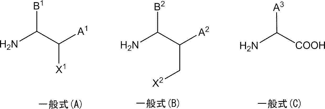
〔一般式(A)中、X1は、-SH、-NH2、または、-OHを表し、A1及びB1は、各々独立に、水素原子または原子数1以上10以下の置換基を表す。但し、A1及びB1が共に水素原子のときは、X1は-SH、または、-OHを表す。
一般式(B)中、X2は、-SH、-NH2、または、-OHを表し、A2及びB2は、各々独立に、水素原子または原子数1以上10以下の置換基を表す。
一般式(C)中、A3は、水素原子または原子数1以上10以下の置換基を表す。〕 - 前記第1の配位子は、主鎖の炭素数が6以上の配位子である請求項13に記載の半導体膜の製造方法。
- 前記半導体量子ドット集合体形成工程と、前記配位子交換工程と、をそれぞれ2回以上行う請求項13または請求項14に記載の半導体膜の製造方法。
- 前記A1、前記B1、前記A2、前記B2、及び前記A3が、各々独立に、水素原子または原子数7以下の置換基である請求項13~請求項15のいずれか1項に記載の半導体膜の製造方法。
- 前記A1、前記B1、前記A2、前記B2、及び前記A3が、水素原子である請求項13~請求項16のいずれか1項に記載の半導体膜の製造方法。
- 前記第2の配位子が、2-アミノエタンチオール、2-アミノエタノール、3-アミノ-1-プロパノール、2-アミノエタンチオール誘導体、2-アミノエタノール誘導体、及び3-アミノ-1-プロパノール誘導体からなる群から選択される少なくとも1種である請求項13~請求項17のいずれか1項に記載の半導体膜の製造方法。
- 前記配位子交換工程では、前記第2の配位子が、前記一般式(A)で表され、前記半導体量子ドット中の金属原子と共に、5員環キレートを形成する請求項13~請求項18のいずれか1項に記載の半導体膜の製造方法。
- 前記半導体量子ドットは、PbS、PbSe、InN、InAs、InSb、及びInPからなる群から選択される少なくとも1つを含む請求項13~請求項19のいずれか1項に記載の半導体膜の製造方法。
- 前記半導体量子ドットは、平均粒径が2nm~15nmである請求項13~請求項20のいずれか1項に記載の半導体膜の製造方法。
- 前記半導体量子ドットは、PbSを含む請求項20または請求項21に記載の半導体膜の製造方法。
- 請求項1~請求項12のいずれか1項に記載の半導体膜を備える太陽電池。
- 請求項1~請求項12のいずれか1項に記載の半導体膜を備える発光ダイオード。
- 請求項1~請求項12のいずれか1項に記載の半導体膜を備える薄膜トランジスタ。
- 請求項1~請求項12のいずれか1項に記載の半導体膜を備える電子デバイス。
Priority Applications (1)
| Application Number | Priority Date | Filing Date | Title |
|---|---|---|---|
| US14/699,817 US10050161B2 (en) | 2012-10-31 | 2015-04-29 | Semiconductor film, method of producing semiconductor film, solar cell, light-emitting diode, thin film transistor, and electronic device |
Applications Claiming Priority (4)
| Application Number | Priority Date | Filing Date | Title |
|---|---|---|---|
| JP2012241230 | 2012-10-31 | ||
| JP2012-241230 | 2012-10-31 | ||
| JP2012-282431 | 2012-12-26 | ||
| JP2012282431A JP6086721B2 (ja) | 2012-10-31 | 2012-12-26 | 半導体膜、半導体膜の製造方法、太陽電池、発光ダイオード、薄膜トランジスタ、および、電子デバイス |
Related Child Applications (1)
| Application Number | Title | Priority Date | Filing Date |
|---|---|---|---|
| US14/699,817 Continuation US10050161B2 (en) | 2012-10-31 | 2015-04-29 | Semiconductor film, method of producing semiconductor film, solar cell, light-emitting diode, thin film transistor, and electronic device |
Publications (1)
| Publication Number | Publication Date |
|---|---|
| WO2014069211A1 true WO2014069211A1 (ja) | 2014-05-08 |
Family
ID=50627125
Family Applications (1)
| Application Number | Title | Priority Date | Filing Date |
|---|---|---|---|
| PCT/JP2013/077668 Ceased WO2014069211A1 (ja) | 2012-10-31 | 2013-10-10 | 半導体膜および半導体膜の製造方法 |
Country Status (3)
| Country | Link |
|---|---|
| US (1) | US10050161B2 (ja) |
| JP (1) | JP6086721B2 (ja) |
| WO (1) | WO2014069211A1 (ja) |
Families Citing this family (5)
| Publication number | Priority date | Publication date | Assignee | Title |
|---|---|---|---|---|
| JP5964744B2 (ja) * | 2012-12-26 | 2016-08-03 | 富士フイルム株式会社 | 半導体膜の製造方法 |
| JP7040445B2 (ja) | 2016-07-20 | 2022-03-23 | ソニーグループ株式会社 | 半導体膜及びその製造方法、並びに、光電変換素子、固体撮像素子及び電子装置 |
| EP3399344B1 (en) * | 2017-05-03 | 2021-06-30 | ams International AG | Semiconductor device for indirect detection of electromagnetic radiation and method of production |
| US11242483B2 (en) * | 2018-09-30 | 2022-02-08 | Tcl Technology Group Corporation | Quantum dot |
| JP7589454B2 (ja) * | 2020-06-17 | 2024-11-26 | artience株式会社 | 光電変換素子及び光電変換層形成用組成物 |
Citations (5)
| Publication number | Priority date | Publication date | Assignee | Title |
|---|---|---|---|---|
| JP2002048795A (ja) * | 2000-07-31 | 2002-02-15 | Mitsubishi Chemicals Corp | オリゴペプチド残基を結合してなる半導体超微粒子 |
| JP2003286292A (ja) * | 2002-01-28 | 2003-10-10 | Mitsubishi Chemicals Corp | 半導体超微粒子及びそれを含有してなる薄膜状成形体 |
| JP2004315661A (ja) * | 2003-04-16 | 2004-11-11 | Mitsubishi Chemicals Corp | 半導体超微粒子及び電界発光素子 |
| JP2009224714A (ja) * | 2008-03-18 | 2009-10-01 | Univ Of Tokyo | 有機薄膜トランジスタの製造方法 |
| WO2011005023A2 (en) * | 2009-07-08 | 2011-01-13 | Samsung Electronics Co., Ltd. | Semiconductor nanocrystal and preparation method thereof |
Family Cites Families (3)
| Publication number | Priority date | Publication date | Assignee | Title |
|---|---|---|---|---|
| EP1116036B1 (en) | 1998-09-18 | 2004-08-11 | Massachusetts Institute Of Technology | Water-soluble fluorescent semiconductor nanocrystals |
| US20040007169A1 (en) | 2002-01-28 | 2004-01-15 | Mitsubishi Chemical Corporation | Semiconductor nanoparticles and thin film containing the same |
| KR20130067137A (ko) * | 2011-12-13 | 2013-06-21 | 삼성전자주식회사 | 양자점-매트릭스 박막 및 그의 제조방법 |
-
2012
- 2012-12-26 JP JP2012282431A patent/JP6086721B2/ja active Active
-
2013
- 2013-10-10 WO PCT/JP2013/077668 patent/WO2014069211A1/ja not_active Ceased
-
2015
- 2015-04-29 US US14/699,817 patent/US10050161B2/en active Active
Patent Citations (5)
| Publication number | Priority date | Publication date | Assignee | Title |
|---|---|---|---|---|
| JP2002048795A (ja) * | 2000-07-31 | 2002-02-15 | Mitsubishi Chemicals Corp | オリゴペプチド残基を結合してなる半導体超微粒子 |
| JP2003286292A (ja) * | 2002-01-28 | 2003-10-10 | Mitsubishi Chemicals Corp | 半導体超微粒子及びそれを含有してなる薄膜状成形体 |
| JP2004315661A (ja) * | 2003-04-16 | 2004-11-11 | Mitsubishi Chemicals Corp | 半導体超微粒子及び電界発光素子 |
| JP2009224714A (ja) * | 2008-03-18 | 2009-10-01 | Univ Of Tokyo | 有機薄膜トランジスタの製造方法 |
| WO2011005023A2 (en) * | 2009-07-08 | 2011-01-13 | Samsung Electronics Co., Ltd. | Semiconductor nanocrystal and preparation method thereof |
Also Published As
| Publication number | Publication date |
|---|---|
| JP6086721B2 (ja) | 2017-03-01 |
| US20150236178A1 (en) | 2015-08-20 |
| US10050161B2 (en) | 2018-08-14 |
| JP2014112623A (ja) | 2014-06-19 |
Similar Documents
| Publication | Publication Date | Title |
|---|---|---|
| JP6177515B2 (ja) | 半導体膜、半導体膜の製造方法、太陽電池、発光ダイオード、薄膜トランジスタ、および、電子デバイス | |
| JP5964744B2 (ja) | 半導体膜の製造方法 | |
| JP5955305B2 (ja) | 半導体膜、半導体膜の製造方法、太陽電池、発光ダイオード、薄膜トランジスタ、および、電子デバイス | |
| JP5964742B2 (ja) | 半導体膜、半導体膜の製造方法、太陽電池、発光ダイオード、薄膜トランジスタ、および、電子デバイス | |
| JP5995661B2 (ja) | 半導体膜、半導体膜の製造方法、太陽電池、発光ダイオード、薄膜トランジスタおよび電子デバイス | |
| Sliz et al. | Stable colloidal quantum dot inks enable inkjet-printed high-sensitivity infrared photodetectors | |
| Zheng et al. | Ultrafast charge transfer from CdSe quantum dots to p-type NiO: hole injection vs hole trapping | |
| Xu et al. | Saturated vapor-assisted growth of single-crystalline organic–inorganic hybrid perovskite nanowires for high-performance photodetectors with robust stability | |
| Zhang et al. | Antimonene quantum dot-based solid-state solar cells with enhanced performance and high stability | |
| JP6086721B2 (ja) | 半導体膜、半導体膜の製造方法、太陽電池、発光ダイオード、薄膜トランジスタ、および、電子デバイス | |
| Geng et al. | Carbon quantum dots interfacial modified graphene/silicon Schottky barrier solar cell | |
| Atiq et al. | Interlayer effect on photoluminescence enhancement and band gap modulation in Ga-doped ZnO thin films | |
| Mishra et al. | Structural, photoconductivity and photoluminescence characterization of cadmium sulfide quantum dots prepared by a co-precipitation method | |
| Tarasenka et al. | Laser-assisted fabrication and modification of copper and zinc oxide nanostructures in liquids for photovoltaic applications | |
| JP6008736B2 (ja) | 半導体膜、半導体膜の製造方法、太陽電池、発光ダイオード、薄膜トランジスタおよび電子デバイス | |
| Thomas et al. | An inverted ZnO/P3HT: PbS bulk-heterojunction hybrid solar cell with a CdSe quantum dot interface buffer layer | |
| Tuc Altaf et al. | Self-Powered Photoelectrochemical Photodetectors Based on a CsPbBr3/S-g-C3N4 Heterojunction-Sensitized 3D ZnO Nanostructured Thin Film | |
| Saleh et al. | Preparation and characterization of CuI/PVA–PEDOT: PSS core–shell for photovoltaic application | |
| JP6275441B2 (ja) | 半導体膜、酸化物微粒子分散液、半導体膜の製造方法、及び、薄膜トランジスタ | |
| Liu et al. | Construction of α-Ga2O3/Nb2CTx heterojunction for self-powered photoelectrochemical solar-blind ultraviolet photodetectors | |
| Wang et al. | Large Orthorhombic Polyhedral CsPbBr3 Nanocrystals for Ultrasensitive Photodetectors with Type‐I Structures | |
| Chen et al. | Dilute manganese-doped ZnO nanowires for high photoelectrical performance | |
| Arul et al. | Titanium oxide decorated zinc oxide nanoparticles for dye-sensitized solar cell and heterojunction diode applications | |
| Shirbeeny et al. | Improved photon trapping by combined use of dye-synthesized and one-dimensional fiber-like nanostructured CuO thin film | |
| García-Carvajal et al. | Synthesis and application of tungsten trioxide nanostructures by doping the active layer of PM6: Y7-based solar cells |
Legal Events
| Date | Code | Title | Description |
|---|---|---|---|
| 121 | Ep: the epo has been informed by wipo that ep was designated in this application |
Ref document number: 13850547 Country of ref document: EP Kind code of ref document: A1 |
|
| NENP | Non-entry into the national phase |
Ref country code: DE |
|
| 122 | Ep: pct application non-entry in european phase |
Ref document number: 13850547 Country of ref document: EP Kind code of ref document: A1 |