WO2014031733A1 - Diketopyrrolopyrrole polymers for electronics and optoelectronics - Google Patents
Diketopyrrolopyrrole polymers for electronics and optoelectronics Download PDFInfo
- Publication number
- WO2014031733A1 WO2014031733A1 PCT/US2013/055967 US2013055967W WO2014031733A1 WO 2014031733 A1 WO2014031733 A1 WO 2014031733A1 US 2013055967 W US2013055967 W US 2013055967W WO 2014031733 A1 WO2014031733 A1 WO 2014031733A1
- Authority
- WO
- WIPO (PCT)
- Prior art keywords
- polymer
- occurrence
- independently selected
- optionally substituted
- hydrogen
- Prior art date
- Legal status (The legal status is an assumption and is not a legal conclusion. Google has not performed a legal analysis and makes no representation as to the accuracy of the status listed.)
- Ceased
Links
Classifications
-
- B—PERFORMING OPERATIONS; TRANSPORTING
- B82—NANOTECHNOLOGY
- B82Y—SPECIFIC USES OR APPLICATIONS OF NANOSTRUCTURES; MEASUREMENT OR ANALYSIS OF NANOSTRUCTURES; MANUFACTURE OR TREATMENT OF NANOSTRUCTURES
- B82Y10/00—Nanotechnology for information processing, storage or transmission, e.g. quantum computing or single electron logic
-
- H—ELECTRICITY
- H10—SEMICONDUCTOR DEVICES; ELECTRIC SOLID-STATE DEVICES NOT OTHERWISE PROVIDED FOR
- H10K—ORGANIC ELECTRIC SOLID-STATE DEVICES
- H10K85/00—Organic materials used in the body or electrodes of devices covered by this subclass
- H10K85/10—Organic polymers or oligomers
- H10K85/111—Organic polymers or oligomers comprising aromatic, heteroaromatic, or aryl chains, e.g. polyaniline, polyphenylene or polyphenylene vinylene
- H10K85/113—Heteroaromatic compounds comprising sulfur or selene, e.g. polythiophene
-
- H—ELECTRICITY
- H10—SEMICONDUCTOR DEVICES; ELECTRIC SOLID-STATE DEVICES NOT OTHERWISE PROVIDED FOR
- H10K—ORGANIC ELECTRIC SOLID-STATE DEVICES
- H10K85/00—Organic materials used in the body or electrodes of devices covered by this subclass
- H10K85/10—Organic polymers or oligomers
- H10K85/151—Copolymers
-
- H—ELECTRICITY
- H10—SEMICONDUCTOR DEVICES; ELECTRIC SOLID-STATE DEVICES NOT OTHERWISE PROVIDED FOR
- H10K—ORGANIC ELECTRIC SOLID-STATE DEVICES
- H10K10/00—Organic devices specially adapted for rectifying, amplifying, oscillating or switching; Organic capacitors or resistors having potential barriers
- H10K10/40—Organic transistors
- H10K10/46—Field-effect transistors, e.g. organic thin-film transistors [OTFT]
- H10K10/462—Insulated gate field-effect transistors [IGFETs]
- H10K10/466—Lateral bottom-gate IGFETs comprising only a single gate
-
- H—ELECTRICITY
- H10—SEMICONDUCTOR DEVICES; ELECTRIC SOLID-STATE DEVICES NOT OTHERWISE PROVIDED FOR
- H10K—ORGANIC ELECTRIC SOLID-STATE DEVICES
- H10K30/00—Organic devices sensitive to infrared radiation, light, electromagnetic radiation of shorter wavelength or corpuscular radiation
- H10K30/30—Organic devices sensitive to infrared radiation, light, electromagnetic radiation of shorter wavelength or corpuscular radiation comprising bulk heterojunctions, e.g. interpenetrating networks of donor and acceptor material domains
-
- H—ELECTRICITY
- H10—SEMICONDUCTOR DEVICES; ELECTRIC SOLID-STATE DEVICES NOT OTHERWISE PROVIDED FOR
- H10K—ORGANIC ELECTRIC SOLID-STATE DEVICES
- H10K30/00—Organic devices sensitive to infrared radiation, light, electromagnetic radiation of shorter wavelength or corpuscular radiation
- H10K30/50—Photovoltaic [PV] devices
-
- H—ELECTRICITY
- H10—SEMICONDUCTOR DEVICES; ELECTRIC SOLID-STATE DEVICES NOT OTHERWISE PROVIDED FOR
- H10K—ORGANIC ELECTRIC SOLID-STATE DEVICES
- H10K85/00—Organic materials used in the body or electrodes of devices covered by this subclass
- H10K85/20—Carbon compounds, e.g. carbon nanotubes or fullerenes
- H10K85/211—Fullerenes, e.g. C60
- H10K85/215—Fullerenes, e.g. C60 comprising substituents, e.g. PCBM
-
- Y—GENERAL TAGGING OF NEW TECHNOLOGICAL DEVELOPMENTS; GENERAL TAGGING OF CROSS-SECTIONAL TECHNOLOGIES SPANNING OVER SEVERAL SECTIONS OF THE IPC; TECHNICAL SUBJECTS COVERED BY FORMER USPC CROSS-REFERENCE ART COLLECTIONS [XRACs] AND DIGESTS
- Y02—TECHNOLOGIES OR APPLICATIONS FOR MITIGATION OR ADAPTATION AGAINST CLIMATE CHANGE
- Y02E—REDUCTION OF GREENHOUSE GAS [GHG] EMISSIONS, RELATED TO ENERGY GENERATION, TRANSMISSION OR DISTRIBUTION
- Y02E10/00—Energy generation through renewable energy sources
- Y02E10/50—Photovoltaic [PV] energy
- Y02E10/549—Organic PV cells
Definitions
- Solution-processable conjugated polymers are of growing interest for low-cost organic electronic devices including field-effect transistors and solar cells. Although progress has been made in developing high mobility p-type polymer semiconductors, device performance including carrier mobility, on/off current ratio and oxidative stability have not been satisfactory.
- Embodiments described herein include compounds, compositions, devices, methods of making, and methods of using.
- a polymer comprising a first repeating unit of formula (I)
- Y at each occurrence is independently selected from O, S, Se and N(R 6 ); and (b) R 6 is independently selected from hydrogen and optionally substituted C1-C30 linear, branched or cyclic organic group.
- the polymer can comprise other monomer units besides that shown in (I).
- A is represented by
- X is S. In one embodiment, m is 1.
- R 1 at each occurrence is independently selected from hydrogen, optionally substituted alkyl, optionally substituted heteroalkyl, fluoroalkyl, and
- R 2 , R 3 , R 4 and R 5 at each occurrence is independently selected from hydrogen, halogen, cyano, optionally substituted alkyl, fluoroalkyl, optionally substituted alkoxy, fluoroalkoxy, optionally substituted thioalkyl, fluorothioalkyl, optionally substituted alkyl sulfoxide, fluoroalkyl sulfoxide, optionally substituted alkyl sulfone, and fluoroalkyl sulfone.
- R 1 at each occurrence is independently selected from C4-C30 linear, branched or cyclic alkyl, and wherein R at each occurrence is independently C4-C30 linear or branched alkoxy.
- R 1 at each occurrence is independently selected from hydrogen and optionally substituted C1-C30 organic group
- R , R 3 , R 4 and R 5 at each occurrence is independently selected from hydrogen, halogen, cyano, and optionally substituted C1-C30 organic group
- the polymer has a Mw of 40,000 Da or more
- A is an electron withdrawing group comprising two or more rings fused together, with two of said rings each comprising at least one imine group.
- A comprises at least two thiazole rings. In one embodiment, A comprises three or more rings fused together. In one embodiment, A is selected from
- W at each occurrence is independently selected from N and C(R 6 );
- Y and Z at each occurrence is independently selected from O, S, Se, P(R 6 ), P(0)R 6 , Si(R 6 ) 2 , C(R 6 ) 2 and N(R 6 );
- R 6 at each occurrence is independently selected from hydrogen, halogen, hydroxyl, cyano, nitro, silyl, siloxanyl, and optionally substituted C 1 -C30 linear, branched or cyclic organic group.
- R 7 and R 8 at each occurrence is independently selected from hydrogen, halogen, cyano, and optionally substituted C4-C30 organic group.
- the first repeating unit is selected from
- the polymer consists essentially of the first repeating unit.
- X at each occurrence is independently selected from O, S and Se;
- m is 0, 1, 2 or 3;
- R 1 at each occurrence is independently selected from hydrogen and optionally substituted C1-C30 organic group;
- R 2 , R 3 , R 4 and R 5 at each occurrence is independently selected from hydrogen, halogen, cyano, and optionally substituted C1-C30 organic group;
- A is an electron withdrawing group comprising two or more rings fused together, with two of said rings each comprising at least one imine group.
- compositions and electronic devices comprising the polymers described herein or made by the method described herein.
- the electronic device is a field effect transistor having a charge carrier mobility of 0.3 cm /Vs or more.
- At least one advantage for some embodiments of the donor-acceptor polymers described herein includes high carrier mobility.
- At least another advantage for some embodiments of the donor-acceptor polymers described herein includes optimal HOMO/LUMO energy levels and more efficient hole injection.
- At least another advantage for some embodiments of the donor-acceptor polymers described herein includes tunable band-gaps which can be optimized for particular applications.
- At least a further advantage for some embodiments of the donor-acceptor polymers described herein includes high melting temperature, if a melting temperature is present.
- At least a further advantage for some embodiments of the donor-acceptor polymers described herein includes high thermal, oxidative and mechanical stabilities.
- At least an additional advantage for some embodiments of the donor-acceptor polymers described herein includes crystallinity and/or ⁇ - ⁇ stacking.
- At least an additional advantage for some embodiments of the donor-acceptor polymers described herein includes good solubility in common organic solvents and good solution processability.
- At least an additional advantage for some embodiments of the donor-acceptor polymer described herein includes that the polymer chains are self-assembled into nanowires having width of several nanometers and length of several nanometers to micrometers.
- Figure 1 shows absorption spectra of PDPTT in CHCI 3 and as a thin film.
- Figure 2 shows cyclic voltammogram of PDPTT film on a platinum electrode in 0.1 mole/L Bu 4 NPF 6 , CH 3 CN solution, (a) Oxidation scans and (b) reduction scans.
- Figure 3a and 3b show the electrical characteristics of PDPTT thin film transistors.
- Figure 4 shows (a) The optical absorption spectrum of PDPTT:PC 7 iBM blend films with the composition of 1 :2, measured from solar cell devices, using ITO/PEDOT substrate as reference, (b) The current density— voltage characteristics of PDPTT:PC7iBM solar cells with a structure of ITO/PEDOT/ PDPTT:PC 7 iBM/LiF/Al under dark and 100 mW/cm2 1.5 AM sun illumination.
- Figure 5 shows EQE spectra of PDPTT :PC7 IBM (1 :2) solar cells.
- Figure 6 shows TEM image of PDPTT :PC7 IBM thin film peeled from solar cells and their SAED patterns (1 :2) are shown as inset.
- Figure 7a and 7b show the electrical characteristics of PDPTTOx thin film transistors.
- Figure 8 show TEM image of PDPTTOx :PC7 IBM thin film peeled from solar cells and their SAED patterns (1 :2) are shown as inset.
- Optionally substituted groups can refer to, for example, functional groups that may be substituted or unsubstituted by additional functional groups.
- groups when a group is unsubstituted, it can be referred to as the group name such as, for example, alkyl or aryl.
- groups when a group is substituted with additional functional groups, it may more generically be referred to as substituted alkyl or substituted aryl (e.g., aralkyl).
- Alkyl can refer to, for example, linear, branched, or cyclic alkyl groups. This term is exemplified by groups such as methyl, ethyl, n-propyl, isopropyl, n-butyl, t-butyl, n-pentyl, ethylhexyl, dodecyl, isopentyl, cyclohexyl, and the like.
- Aryl can refer to, for example, aromatic carbocyclic groups having one or more single rings (e.g., phenyl or biphenyl) or multiple condensed rings (e.g., naphthyl or anthryl).
- Heteroalkyl can refer to, for example, an alkyl group wherein one or more carbon atoms are substituted with heteroatoms.
- Heteroaryl can refer to, for example, an aryl group wherein one or more carbon atoms are substituted with heteroatoms.
- Fluoroalkyl can refer to, for example, an alkyl group wherein one or more hydrogen atoms are substituted with fluoro. Fluoroalkyl described herein include perfluoroalkyl as well as partially fluorinated alkyl.
- Fluoroalkoxide can refer to, for example, an alkoxide group wherein one or more hydrogen atoms are substituted with fluoro. Fluoroalkoxide described herein include perfluoroalkoxide group as well as partially fluorinated alkoxide.
- Haloalkyl can refer to, for example, an alkyl, alkenyl group or alkynyl group wherein one or more hydrogen atoms are substituted with halogen.
- silica can refer to, for example, a group of formula -SiR R R , wherein R , R and R are each independently a Ci-C 8 alkyl group.
- Siloxanyl can refer to, for example, a group of formula -O-SiR R R , wherein R , R and R are each independently a Ci-C 8 alkyl group.
- the first repeating unit comprises a strong electron accepting diketopyrrolopyrrole group, a weak electron accepting group comprising at least two imine moieties, and at least two electron donating thiophene/furan/selenophene groups.
- the first repeating unit is represented by formula (I):
- each X is independently selected from O, S and Se;
- m is 0, 1, 2 or 3;
- R 1 at each occurrence is independently selected from hydrogen and optionally substituted C 1 -C30 organic group;
- R 2 , R 3 , R 4 and R 5 at each occurrence is independently selected from hydrogen, halogen, cyano, and optionally substituted C 1 -C30 organic group;
- A is an electron withdrawing group comprising two or more imine moieties.
- the first repeating unit can be represented by
- the first repeating unit can be represented by
- the first repeating unit can be represented by
- A is a heteroaryl group comprising two or more rings fused together, with two of said rings each comprising at least one imine group. In some embodiments, A comprises three or more rings fused together. In some embodiments, A comprises at least two thiazole or oxazole rings fused together. In some embodiments, A comprises at least two thiazole or oxazole rings and a third ring fused together.
- A can be selected from, for exam le, the following:
- each W is independently selected from N and C(R 6 );
- each Y and Z is independently selected from O, S, Se, P(R 6 ), P(0)R 6 , Si(R 6 ) 2 , C(R 6 ) 2 and N(R 6 ); and
- each R 6 is independently selected from hydrogen, halogen, hydroxyl, cyano, nitro, silyl, siloxanyl, and an optionally substituted C1-C30 linear, branched or cyclic organic group.
- R 6 can be, for example, hydrogen, halogen, hydroxyl, cyano, nitro, silyl, siloxanyl, or an optionally substituted C1-C30 organic group selected from alkyl, cycloalkyl, aralkyl, alkenyl, cycloalkenyl, alkynyl, mercapto, alkoxy, alkylthio, aryl, aryl ether, aryl thioether, heterocyclic, haloalkyl, haloalkenyl, haloalkynyl, aldehyde, carboxyl, ester, carbomyl or vinyl group.
- R 6 can be, for example, hydrogen, a linear or branched C1-C24, C1-C18 or C1-C12 alkyl group, or a linear or branched C1-C24, C1-C18 or C1-C12 heteroalkyl group.
- R 6 can be, for example, hydrogen, a C1-C24, Ci-Cig or C ⁇ -Cn linear or branched fluoroalkyl group, or a Cj- C 2 4, Ci-Cig or C1-C12 linear or branched fluoroalkoxide group.
- A is a thiazolothiazole represented by -i N.X Sr-
- A is an optionally substituted benzobisthiazole represented
- each R 7 is independently selected from hydrogen, halogen, cyano, and optionally substituted C4-C30 organic group.
- each R 7 is a C4-C30 linear or branched alkyl, alkoxide, fluoroalkyl or fluoroalkoxide.
- A does not include the structure XXX.
- A is an optionally substituted benzobisoxazole represented by
- each R is independently selected from hydrogen, halogen, cyano, and optionally substituted C4-C30 organic group.
- each R is independently selected from hydrogen, halogen, cyano, and optionally substituted C4-C30 organic group.
- R is a C4-C30 linear or branched alkyl, alkoxide, fluoroalkyl or fluoroalkoxide. In one embodiment, A does not include the structure XXXX.
- X is S and the polymer comprises at least two, at least four, or at least six thiophene groups. In some embodiments, X is Se and the polymer comprises at least two, at least four or at least six selenophene groups. In some embodiments, X is O and the polymer comprises at least two, at least four or at least six furan groups.
- R 1 can be independently selected from hydrogen, optionally substituted alkyl, optionally substituted heteroalkyl, fluoroalkyl, and fluoroheteroalkyl
- R 2 , R 3 , R 4 and R 5 can be independently selected from, for example hydrogen, halogen, cyano, optionally substituted alkyl, fluoroalkyl, optionally substituted alkoxy, fluoroalkoxy, optionally substituted thioalkyl, fluorothioalkyl, optionally substituted alkyl sulfoxide, fluoroalkyl sulfoxide, optionally substituted alkyl sulfone, and fluoroalkyl sulfone,.
- R 3 and R 5 are hydrogen. In some embodiments, R 3 , R 4 and R 5 are hydrogen, and the first repeating unit can be represented by formula (V): (V). Further, wherein X is S and m is 1, the first repeating unit can be represented by formula (VI):
- R and R are independently selected from a linear or branched C4-C24, C4-C18 or C4-C12 alkyl group and a linear or branched C4-C24, C4-C18 or C4-C12
- R and R are independently selected from a C 4 - C24, C4-C18 or C4-C12 linear or branched fluoroalkyl group and a C4-C24, C4-C18 or C4-C12 linear or branched fluoroalkoxide group.
- each R 1 is a C4- alkyl
- each R 2 is a C4- alkyl
- C30 linear or branched is a C4-C30 linear or branched heteroalkyl such as alkoxy, and each R 3 , R 4 and R 5 is hydrogen.
- the donor-acceptor polymer comprises a first repeating
- W is N and Y is selected from O, S, Se and N(R 6 ).
- A is thiazolothiazole.
- X is S and m is 1
- the first repeating unit can be represented by formula (VII): (VII).
- each R 1 and R 2 is a C4-C30 linear or branched alkyl group or a C4-C30 linear or branched heteroalkyl group such as alkoxy.
- the donor-acceptor polymer consists essentially of the first repeating unit. In other embodiments, the donor-acceptor polymer further comprises a second repeating unit and/or a third repeating unit different from the first repeating unit described herein.
- the second and third repeating units can be, for example, independently selected from electron-donating groups and electron- withdrawing groups known in the art.
- the donor-acceptor polymer can be, for example, a homopolymer of the first repeating unit.
- the donor-acceptor polymer can also be, for example, a copolymer such as a block copolymer or an alternating copolymer.
- the molar percentage of the first repeating unit in the polymer can be, for example, at least 50%, or at least 70%, or at least 90%, or at least 95%, or at least 98%.
- the donor-acceptor polymer described herein can have a weight-average molecule weight (M w ) of, for example, at least 30,000 Da, at least 40,000 Da, at least 50,000 Da, at least 60,000 Da, at least 80,000 Da, or at least 100,000 Da.
- M w weight-average molecule weight
- the upper limit for M w can be, for example, 250,000 Da or 1,000,000 Da.
- the donor-acceptor polymer described herein can have a number-average molecule weight (M n ) of, for example, at least 10,000 Da, at least 15,000 Da, at least 18,000 Da, at least 20,000 Da, or at least 30,000 Da.
- the upper limit for M n can be, for example, 100,000 Da or 300,000 Da.
- the donor-acceptor polymer described herein can have good solubility in common organic solvents such as chloroform, chlorobenzene, dichlorobenzene, etc.
- the donor-acceptor polymer is soluble in chloroform, chlorobenzene and dichlorobenzene at room temperature.
- the solubility of the donor-acceptor polymer in CHCI 3 at room temperature can be, for example, at least 10 mg/mL or at least 15 mg/mL, or at least 1 wt.% or at least 1.5 wt.%.
- the upper limit for said solubility in CHCI 3 at room temperature can be, for example, 100 mg/mL or 10 wt.%.
- the conjugated copolymers can have tunable "charge transfer", absorption bands in the UV or UV-visible or infra red region, HOMO/LUMO energy levels and charge carrier mobilities.
- the electron deficient "A" group which comprises two or more imine moieties in a fused polycyclic ring, can be conjugated with the
- the donor-acceptor polymer described herein can be made by, for example, Stille coupling using di-tin monomers or Suzuki coupling using borate ester groups.
- Known catalysts including palladium complexes can be used.
- the polymer described herein can be made by reacting a first
- R" is alkyl
- X is S
- m is 1
- A is thiazolothiazole
- the first compound can be synthesized according to the followin scheme.
- the first compound can be s nthesized according to the following scheme.
- Br— ⁇ ⁇ Br made by reacting a first compound re resented by Br- A- Br such as S N with
- the polymers described herein can be used to fabricate novel organic electronic devices, including organic light emitting diodes (OLEDs), transistors, and solar cells.
- the fabrication process often includes the formation of a film of the polymers described herein on a substrate, and one embodiment is a coated substrate.
- Organic films of the polymer described herein can be prepared by known methods such as spin coating, casting, dip coating, inkjet, doctor blade coating, screen printing, and spray coating. Using these methods, one can prepare organic films having good properties such as mechanical strength, toughness, and durability without forming cracks in the films.
- the organic films can be suitable for use in organic electronic devices such as FET elements, photovoltaic cells, and light emitting elements.
- Films of the copolymer described herein are typically prepared by coating a coating liquid, which is prepared by dissolving the copolymer in a solvent such as dichloromethane, tetrahydrofuran, chloroform, toluene, chlorobenzene, dichlorobenzene, or xylene, on a substrate.
- a coating liquid which is prepared by dissolving the copolymer in a solvent such as dichloromethane, tetrahydrofuran, chloroform, toluene, chlorobenzene, dichlorobenzene, or xylene
- Specific examples of the coating methods include spray coating, spin coating, blade coating, dip coating, cast coating, roll coating, bar coating, die coating, ink jet, dispense methods, etc.
- a proper method and a proper solvent can be selected taking into consideration of the properties of the polymer used.
- Suitable materials for use as the substrate on which a film of the polymer of the present invention is formed include inorganic substrates such as glass plates, silicon plates, ITO plates, and FTO plates, and organic substrates such as plastic plates (e.g., PET films, polyimide films, and polystyrene films) , which can be optionally subjected to a surface treatment.
- inorganic substrates such as glass plates, silicon plates, ITO plates, and FTO plates
- organic substrates such as plastic plates (e.g., PET films, polyimide films, and polystyrene films) , which can be optionally subjected to a surface treatment.
- plastic plates e.g., PET films, polyimide films, and polystyrene films
- a substrate with a smooth surface is used.
- the thickness of the organic film and the organic semiconductor layer of the organic thin film transistor of the present invention are not particularly limited. However, the thickness can be determined such that the resultant film or layer is a uniform thin layer (i.e., the film or layer can be substantially free of gaps or holes which can adversely affect the carrier transport property thereof).
- the thickness of the organic semiconductor layer can be, for example, not greater than 1 micron, and preferably about 5-200 nm.
- the field-effect transistor comprises a thin- film of the copolymer.
- the thin film can be deposited from a solution of the copolymer.
- the thin-film can be fabricated by spin coating.
- the thin-film can be fabricated by vacuum vapor deposition.
- the field-effect transistor can be a p-channel transistor.
- the electron mobility of the field-effect transistor can be, for example, -3 2 -2 2
- the on/off current ratio of the field-effect transistor can be, for example, at least 10 4 , or at least 10 5 , or at least 10 6 , or about 10 4 -10 7 , or about 10 5 -10 6 .
- the organic thin film transistors of described herein can have a configuration such that an organic semiconductor layer including the copolymer described herein is formed therein while also contacting the source electrode, drain electrode and insulating layer of the transistor.
- the organic thin film transistor prepared above can be thermally annealed. Annealing can be performed while the film is set on a substrate, and is believed (without wishing to be bound by theory) to allow for at least partial self-ordering and/or ⁇ -stacking of the copolymers to occur in the solid state.
- the annealing temperature is determined depending on the property of the polymer, but is preferably from room temperature to 300 °C, and more preferably from 50 to 300 °C. In some embodiments, thermal annealing is carried out at least 150 °C, or preferably above 170 °C, or above 200 °C. When the annealing temperature is too low, the organic solvent remaining in the organic film cannot be well removed therefrom.
- the organic film can be thermally decomposed.
- Annealing is preferably performed in a vacuum, or under nitrogen, argon or air atmosphere.
- annealing is performed in an atmosphere including a vapor of an organic solvent capable of dissolving the polymer so that the molecular motion of the polymer is accelerated, and thereby a good organic thin film can be prepared.
- the annealing time can be properly determined depending on the aggregation speed of the polymer.
- An insulating (dielectric) layer can be used in the organic thin film transistors comprising the copolymers described herein, situated between the gate electrode and the organic thin film comprising the polymers.
- Various insulating materials can be used for the insulating layer.
- Specific examples of the insulating materials include inorganic insulating materials such as silicon oxide, silicon nitride, aluminum oxide, aluminum nitride, titanium oxide, tantalum oxide, tin oxide, vanadium oxide, barium strontium titanate, barium zirconate titanate, lead zirconium titanate, lead lanthanum titanate, strontium titanate, barium titanate, barium magnesium fluoride, bismuth tantalate niobate, hafnium oxide, and trioxide yttrium; organic insulating materials such as polymer materials, e.g., polyimide, polyvinyl alcohol, polyvinyl phenol, polystyrene, polyester, polyethylene, polyphenylene
- Suitable methods for forming such an insulating layer include dry processes such as CVD methods, plasma CVD methods, plasma polymerization methods, and vapor deposition methods; wet processes such as spray coating methods, spin coating methods, dip coating methods, inkjet coating methods, cast coating methods, blade coating methods, and bar coating methods; etc.
- an organic thin film (intermediate layer) can be employed between the insulating layer and organic semiconductor layer.
- the materials for use in the intermediate layer are not particularly limited as long as the materials do not chemically affect the properties of the organic semiconductor layer, and for example, molecular films of organic materials, and thin films of polymers can be used therefor.
- Specific examples of the materials for use in preparing the molecular films include coupling agents such as octadecyltrichlorosilane, octyltrichlorosilane, octyltrimethoxysilane, hexamethyldisilazane (HMDS), and
- polymers for use in preparing the polymer films include the polymers mentioned above for use in the insulating layer. Such polymer films can serve as the insulating layer as well as the intermediate layer.
- the materials of the electrodes (such as gate electrodes, source electrodes and drain electrodes) of the organic thin film transistor described herein are not particularly limited as long as the materials are electrically conductive.
- Specific examples of the materials include metals such as platinum, gold, silver, nickel, chromium, copper, iron, tin, antimony, lead, tantalum, indium, aluminum, zinc, tungsten, titanium, calcium, and magnesium; alloys of these metals; electrically conductive metal oxides such as indium tin oxide (ITO); inorganic or organic semiconductors, whose electroconductivity is improved by doping or the like, such as silicon single crystal, polysilicon, amorphous silicon, germanium, graphite, carbon nanotube, polyacetylene, polyparaphenylene, polythiophene, polypyrrole, polyaniline, polythienylenevinylene, polyparaphenylenevinylene, and complexes of
- PEDOT polyethylenedioxythiophene
- polystyrene sulfonic acid polystyrene sulfonic acid
- Solar cells and photovoltaic cells described herein can be fabricated by first spin- coating a PEDOT buffer layer on top of ITO-coated glass substrates (10 ⁇ /sq, Shanghai B. Tree Tech. Consult Co. Ltd., Shanghai, China) at 3000 rpm for 40 s and drying at 150°C for 10 min under vacuum.
- the thickness of PEDOT can be, for example, around 40 nm.
- the active layer of the solar cells comprising the polymers described herein can comprise a mixed "heterojunction" active layer that is a phase separated blend of the polymers or copolymers described herein and an electron acceptor material.
- the electron acceptor material can comprise a variety of organic materials (small molecules, oligomers, polymers, or copolymers) that have a LUMO energy level that is at least about 0.2 to 0.6 eV more negative than the LUMO energy level of the copolymers described herein, and a HOMO energy level that is more negative than the HOMO energy level of the copolymers described herein.
- the electron acceptor material can be a fullerene or a modified fullerene (e.g., C6i-phenyl-butyric acid methyl ester, PC 6 iBM, or C 7 i-phenyl- butyric acid methyl ester, PC 7 iBM).
- the electron acceptor material can be an electron accepting semiconducting organic small molecule, oligomer, or polymer having appropriate LUMO and HOMO energies (at least about 0.2-0.6 eV more negative than the LUMO energy level and a more negative HOMO energy level than the HOMO energy level of the copolymers described herein).
- electron acceptor materials include small molecules, oligomers, polymers, or copolymers having highly electron deficient functional groups, such as naphthalene diimide, perylene diimide, rylene, phthalimide, and related derivatives comprising electron accepting groups.
- a composition comprising a solution or dispersion of one or more of the polymers or copolymers described herein and one or more acceptor materials (for example fullerene derivatives) is spin-coated on top of the PEDOT layer, for example at a speed of 1000 rpm for 30 seconds, to form a layer comprising the one or more copolymers and one or more electron accepting materials.
- the solution or dispersion is applied using a hot solvent, and dried under vacuum immediately after the deposition the copolymers.
- the coated device precursor can then be annealed, for example on a hot plate at 150 ⁇ 10 °C for 10 min in a glove box, to form the active layer.
- the active layer can also be spin-coated in air and dried in a vacuum oven without thermal annealing.
- the solvents used for dissolving the mixture of copolymers described herein and the electron acceptors can be chloroform, chlorobenzene, 1 ,2-dichlorbenzene, etc.
- the solvents for copolymer/fullerene blend can be a single solvent such as chloroform, chlorobenzene, 1 ,2-dichlorbenzene or a mixture of two or three different solvents
- the second (third) solvent can be 1,8-diiodooctane, 1,8-dibromoctane, 1,8-octanedithiol, etc.
- the solvents can be heated so as to increase the solubility of the polymer and/or electron acceptor, as an aid to film formation.
- Thermal annealing is believed to induce at least partial phase separation between the polymers described herein and the electron acceptors, forming the "heterojunctions" on the nanometer scale that are believed to be the site of light-induced charge separation.
- the solar cell precursors comprising the polymer-coated substrates can be taken out of the glove box and loaded in a thermal evaporator (BOC Edwards, 306) for the deposition of the cathode.
- the cathode consisting of 1.0 nm LiF and 80 nm aluminum layers can be sequentially deposited through a shadow mask on top of the active layers in a vacuum of 8xl0 "7 torr.
- each substrate contains 4 solar cells with an active area of 9 mm .
- the starting materials 1 (398 mg, 0.4 mmol) and 2 (376 mg, 0.4 mmol), and catalyst tris(dibenzylideneacetone)dipalladium (0) (8 mg, 0.009 mmol) and tri-o-tolylphosphine (11 mg, 0.04 mmol) in anhydrous chlorobenzene (38 mL) were heated at reflux for 3 days. Then the heating was reduced to 50 °C; the reaction mixture was poured into 200 mL of methanol containing 5 mL of hydrochloric acid and stirred for 5 hours. The black precipitate was collected via filtration, and was further purified by Soxhlet extraction with methanol and hexane.
- the thermal behavior of PDPTT copolymer was investigated by differential scanning calorimetry (DSC) and thermogravimetric analysis (TGA).
- DSC differential scanning calorimetry
- TGA thermogravimetric analysis
- PDPTT was highly soluble in almost all organic solvents such as chloroform, chlorobenzene and dichlorobenzene at room temperature.
- the absorption maximum in dilute solution of CHC1 3 ( ⁇ 10 ⁇ 6 M) was found to be 686 and 736 nm ( Figure 1).
- the absorption spectrum of the thin films was slightly red shifted and showed a peak maximum at 749 and a vibronic shoulder at 688 nm.
- the optical band gap measured at the absorption edge of the film was calculated to be 1.38 eV.
- the HOMO and LUMO energy level of PDPTT was estimated from cyclic voltammetry (CV) results ( Figure 2).
- the electrochemical band gap of the polymer PDPTT was 1.61 eV
- Example 2 Transistors and Solar Cells Comprising PDPTT
- Thin film OFETs utilizing PDPTT as an organic semiconductor were fabricated in conventional top-contact, bottom-gate geometry.
- the channel widths and lengths of the devices were 400 or 1000 ⁇ and 20-100 ⁇ , respectively.
- the surface of the silicon dioxide was cleaned and treated with octyltrichlorosilane (OTS8).
- OTS8 octyltrichlorosilane
- PDPTT copolymer was spun onto hydrophobically modified oxide from a solution in 1,2,-dichlorobenzene and the resulting thin film OFETs were then annealed at 200 °C for 10 min under inert atmosphere.
- I ds ⁇ C 0 W/2L)(V g -V t ) .
- the output and transfer characteristics of the OFETs are shown in Figures 3 a and 3b.
- the PDPTT OFETs showed p-channel characteristics with a large current modulation (I on /Ioff
- PDPTT had an average hole mobility of 0.45 cm /Vs .
- the average threshold voltage (V t ) of PDPTT was -29.3 V.
- Photovoltaic cells comprising a 1 :2 blend of PDPTT and PC 71 BM were fabricated.
- the films were spin-coated from a solution of PDPTT:PC 7 iBM blend and the solvent was a mixture of o-dichlorobenzene (ODCB) and 1,8-diiodooctane (DIO).
- ODCB o-dichlorobenzene
- DIO 1,8-diiodooctane
- the blend films were dried under vacuum at room temperature for a certain period of time.
- UV-Vis absorption spectra PDPTT: PC 71 BM (1 :2) blend films on glass/ITO/PEDOT substrates are shown in Figure 4a.
- the EQE spectra of the devices are shown in Figure 5.
- the PDPTT:PC 71 BM device showed photoconversion efficiency with a monochromatic EQE around 30% over the 350- 580 wavelength range.
- the calculated J sc by integrating the EQE curve of PDPTT:PC 7 iBM solar cell with an AMI .5G reference spectrum is 7.62 mA/cm (in the wavelength range of 350-580 nm) compared with 8.0 mA/cm measured on same size device; thus, the spectral mismatch factor was ⁇ 5%.
- the dibromo compound 1 (337 mg, 0.37 mmol) and distannyl compound 3 (330 mg, 0.37 mmol, prepared according to Subramaniyan et al, Adv. Ener. Mater. 2011, 1, 854-860) and catalyst tris(dibenzylideneacetone)dipalladium (0) (7 mg, 0.007 mmol) and tri-o- tolylphosphine (9 mg, 0.03 mmol) in anhydrous chlorobenzene (10 mL) were heated at 120 °C for 72 hours. The temperature was then reduced to 55°C. The reaction mixture was poured into 200 mL of methanol containing 5 mL of hydrochloric acid and stirred for 5 hours.
- PDPTTOx was highly soluble in chloroform, chlorobenzene, and dichlorobenzene at room temperature.
- the absorption maximum in dilute solution of CHC1 3 ( ⁇ 10 ⁇ 6 M) was found to be 799 nm.
- the absorption spectrum of the thin films was red shifted and showed a broad absorption maximum at 769 and 818 nm.
- the optical band gap measured at the absorption edge of the film was calculated to be 1.22 eV.
- the HOMO level of PDPTTOx was estimated from cyclic voltammetry (CV) results .
- the onset oxidation and reduction potential was 0.74 V and -0.90 V (versus SCE), from which the HOMO and LUMO level of the polymer were calculated to be 5.14 eV and 3.50 eV, respectively.
- the electrochemical band gap of the polymer PDPTTOx was 1.64 eV.
- Example 4 Transistors and Solar Cells Comprising PDPTTOx
- PDPTTOx charge transport properties of PDPTTOx were investigated by fabricating OFETs with conventional top-contact and bottom-gate geometry on top of silicon (gate) and silicon dioxide (dielectric) substrates and patterned gold source/drain electrodes.
- the typical output and transfer characteristics of PDPTTOx OFETs are shown in Figure 7a and 7b.
- Photovoltaic cells comprising a 1 :2 blend of PDPTTOx and PC 71 BM were fabricated.
- UV-Vis absorption spectra PDPTTOx: PC 71 BM (1 :2) blend films were measured on glass/ITO/PEDOT substrates.
- the current density (J sc ), open circuit voltage (V), and fill factor (FF) achieved in the PDPTTOx:PC 7 iBM (1 :2) solar cell were 8.31 mA/cm 2 , 0.52 V, and 0.51, respectively, with a power conversion efficiency of 2.16%.
- the PDPTTOx:PC 7 iBM device showed photoconversion efficiency with a monochromatic EQE around 30% over the 350-580 wavelength range.
- the calculated J sc by integrating the EQE curve of PDPTTOx:PC 7 iBM solar cell with an AM1.5G reference 2
- PDPBT The dibromo compound 1 (380 mg, 0.42 mmol), and di-tin compound 4 (428 mg, 0.42 mmol) and catalyst tris(dibenzylideneacetone)dipalladium (0) (8 mg, 0.008 mmol) and tri-o-tolylphosphine (10 mg, 0.017 mmol) in anhydrous chlorobenzene (20 mL) were heated at reflux for 30 hours. Then the heating was reduced to 50° C; the reaction mixture was poured into 200 mL of methanol containing 5 mL of hydrochloric acid and stirred for 5 hours. The black precipitate was collected via filtration, and was further purified by Soxhlet extraction with methanol and hexane.
- PDPBT was soluble in chloroform solution at room temperature and soluble in chlorobenzene and dichlorobenzene at 100 C.
- the absorption maximum in solution in dilute CHCI 3 ( ⁇ 10 ⁇ 6 M) was found to be 668 and 723 nm.
- the absorption spectrum of the thin films was red shifted and showed a broad absorption maximum at 673 and 743 nm.
- the optical band gap measured at the absorption edge of the film was calculated to be 1.33 eV.
- the HOMO level of PDPBT was estimated from cyclic voltammetry (CV) results.
- the onset oxidation and reduction potential was 0.91 V and -0.92 V (versus SCE), from which the HOMO and LUMO level of the polymer were calculated to be 5.31 eV and 3.48 eV, respectively.
- the electrochemical band gap of the polymer PDPBT was 1.83 eV.
- the channel widths of the devices were 400-1000 ⁇ and lengths were 20-100 ⁇ .
- the surface of the silicon dioxide was cleaned and treated with octyltrichlorosilane (OTS8). Polymer solutions were spun onto a substrate. Thin films were then annealed at 200 °C for 10 min under inert atmosphere.
- Solar cells using PDPBT as donor and PC 71 BM as acceptor components were fabricated.
- the active layer of the solar cells were spin-coated from PDPBT:PC 7 iBM (1 :2 w wt) blend solution in chloroform on top of PEDOT:PSS coated ITO substrates.
- the solar cell devices were finished by deposition of the cathodes, consisting of 1 nm LiF and 80 nm Al, in a thermal evaporator.
- the spin-coating of the active layer was performed in a glove box and the films were annealed at 150°C for 10 min.
- the solar cells had an active area of 9 mm 2 .
- the PDPBT:PC 7 iBM device showed photoconversion efficiency with a
- FT-IR spectra were obtained from Perkin Elmer 1720 FT-IR spectrophotometer with KBr pellets. Mass spectra were recorded on a Bruker Esquire LC/ Ion Trap Mass spectrometer. 1 H-NMR spectra were recorded on a Bruker AV300/AV500 at 300 MHz/500 MHz respectively using CDC1 3 or C 6 D 4 C1 2 or CF 3 COOD as the solvents.
- GPC Gel Permeation Chromatography
- Silver/silver ion (Ag in 0.1 M AgN0 3 solution, Bioanalytical System, Inc.) was used as a reference electrode. Ferrocene/ferrocenium (Fc/Fc + ) was used as an internal standard. The potential values obtained in reference to Ag/Ag + were converted to the saturated calomel electrode (SCE) scale. Thin film cyclic voltammetry was performed in acetonitrile containing 0.1M TBAPF 6 . UV-vis absorption spectra were recorded on a Perkin- Elmer model Lambda 900 UV/vis/near-IR spectrophotometer. The photoluminescence (PL) emission spectra were obtained with a Photon Technology International (PTI) Inc.
- PL photoluminescence
Landscapes
- Engineering & Computer Science (AREA)
- Chemical & Material Sciences (AREA)
- Nanotechnology (AREA)
- Materials Engineering (AREA)
- Physics & Mathematics (AREA)
- Mathematical Physics (AREA)
- Theoretical Computer Science (AREA)
- Crystallography & Structural Chemistry (AREA)
- Thin Film Transistor (AREA)
- Polyoxymethylene Polymers And Polymers With Carbon-To-Carbon Bonds (AREA)
Abstract
Provided here are diketopyrrolopyrrole-based polymers comprising electron accepting subunits such as thiazolothiazole, benzobisthiazole or benzobisoxazole rings, and electron donating subunits such as certain heterocyclic groups. The polymers are useful for manufacturing organic electronic devices, including transistors and solar cells. Methods for making the polymers and the electronic devices comprising the polymers are also described.
Description
DIKETOPYRROLOPYRROLE POLYMERS FOR ELECTRONICS AND
OPTOELECTRONICS
This invention was made with government support under DMR-0805259 awarded by the National Science Foundation. The government has certain rights in the invention.
BACKGROUND
Solution-processable conjugated polymers are of growing interest for low-cost organic electronic devices including field-effect transistors and solar cells. Although progress has been made in developing high mobility p-type polymer semiconductors, device performance including carrier mobility, on/off current ratio and oxidative stability have not been satisfactory.
Thus, a need exists for developing new p-type polymer semiconductors that are suitable for use in high performance organic electronic devices including field-effect transistors and solar cells.
SUMMARY
Embodiments described herein include compounds, compositions, devices, methods of making, and methods of using.
For example, provided is a polymer comprising a first repeating unit of formula (I)

N wherein (a) Y at each occurrence is independently selected from O, S, Se and N(R6); and (b) R6 is independently selected from hydrogen and optionally substituted C1-C30
linear, branched or cyclic organic group. The polymer can comprise other monomer units besides that shown in (I).
In one embodiment, A is represented by

In one embodiment, X is S. In one embodiment, m is 1.
In one embodiment, R1 at each occurrence is independently selected from hydrogen, optionally substituted alkyl, optionally substituted heteroalkyl, fluoroalkyl, and
fluoroheteroalkyl; and R2, R3, R4 and R5 at each occurrence is independently selected from hydrogen, halogen, cyano, optionally substituted alkyl, fluoroalkyl, optionally substituted alkoxy, fluoroalkoxy, optionally substituted thioalkyl, fluorothioalkyl, optionally substituted alkyl sulfoxide, fluoroalkyl sulfoxide, optionally substituted alkyl sulfone, and fluoroalkyl sulfone.
In another embodiment, R1 at each occurrence is independently selected from C4-C30 linear, branched or cyclic alkyl, and wherein R at each occurrence is independently C4-C30 linear or branched alkoxy.
Also provided is a polymer comprising a first repeating unit of formula (I)

independently selected from O, S and Se; (ii) m is 0, 1, 2 or 3; (iii) R1 at each occurrence is independently selected from hydrogen and optionally substituted C1-C30 organic group; R , R3, R4 and R5 at each occurrence is independently selected from hydrogen, halogen, cyano, and optionally substituted C1-C30 organic group; (iv) the polymer has a Mw of 40,000 Da or more; and (v) A is an electron withdrawing group comprising two or more rings fused together, with two of said rings each comprising at least one imine group.
In one embodiment, A comprises at least two thiazole rings. In one embodiment, A comprises three or more rings fused together.
In one embodiment, A is selected from
wherein: (i) W at each occurrence is independently selected from N and C(R6); (ii) Y and Z at each occurrence is independently selected from O, S, Se, P(R6), P(0)R6, Si(R6)2, C(R6)2 and N(R6); and (iii) R6 at each occurrence is independently selected from hydrogen, halogen, hydroxyl, cyano, nitro, silyl, siloxanyl, and optionally substituted C1-C30 linear, branched or cyclic organic group.
In one embodiment, wherein A is selected from

In one embodiment, the first repeating unit is selected from


In one embodiment, the polymer consists essentially of the first repeating unit.
Further provided is a method for making the polymers described herein, comprising

reacting a first compound represented b R2 R3 or R2 R3 with
a second compound represented by

wherein: (i) X at each occurrence is independently selected from O, S and Se; (ii) m is 0, 1, 2 or 3; (iii) R1 at each occurrence is independently selected from hydrogen and optionally substituted C1-C30 organic group; R2, R3, R4 and R5 at each occurrence is independently selected from hydrogen, halogen, cyano, and optionally substituted C1-C30 organic group; and
(iv) A is an electron withdrawing group comprising two or more rings fused together, with two of said rings each comprising at least one imine group.
Additionally provided are compositions and electronic devices comprising the polymers described herein or made by the method described herein. In a particular embodiment, the electronic device is a field effect transistor having a charge carrier mobility of 0.3 cm /Vs or more.
At least one advantage for some embodiments of the donor-acceptor polymers described herein includes high carrier mobility.
At least another advantage for some embodiments of the donor-acceptor polymers described herein includes optimal HOMO/LUMO energy levels and more efficient hole injection.
At least another advantage for some embodiments of the donor-acceptor polymers described herein includes tunable band-gaps which can be optimized for particular applications.
At least a further advantage for some embodiments of the donor-acceptor polymers described herein includes high melting temperature, if a melting temperature is present.
At least a further advantage for some embodiments of the donor-acceptor polymers described herein includes high thermal, oxidative and mechanical stabilities.
At least an additional advantage for some embodiments of the donor-acceptor polymers described herein includes crystallinity and/or π-π stacking.
At least an additional advantage for some embodiments of the donor-acceptor polymers described herein includes good solubility in common organic solvents and good solution processability.
At least an additional advantage for some embodiments of the donor-acceptor polymer described herein includes that the polymer chains are self-assembled into nanowires having width of several nanometers and length of several nanometers to micrometers.
Other advantages for at least some embodiments include broad absorption bands (-500 nm to 900-1000 nm) and low optical band gaps (1.2-1.4 eV) for maximum light harvesting in solar cells.
BRIEF DESCRIPTION OF THE DRAWINGS
Figure 1 shows absorption spectra of PDPTT in CHCI3 and as a thin film.
Figure 2 shows cyclic voltammogram of PDPTT film on a platinum electrode in 0.1 mole/L Bu4NPF6, CH3CN solution, (a) Oxidation scans and (b) reduction scans.
Figure 3a and 3b show the electrical characteristics of PDPTT thin film transistors.
Figure 4 shows (a) The optical absorption spectrum of PDPTT:PC7iBM blend films with the composition of 1 :2, measured from solar cell devices, using ITO/PEDOT substrate as reference, (b) The current density— voltage characteristics of PDPTT:PC7iBM solar cells with a structure of ITO/PEDOT/ PDPTT:PC7iBM/LiF/Al under dark and 100 mW/cm2 1.5 AM sun illumination.
Figure 5 shows EQE spectra of PDPTT :PC7 IBM (1 :2) solar cells.
Figure 6 shows TEM image of PDPTT :PC7 IBM thin film peeled from solar cells and their SAED patterns (1 :2) are shown as inset.
Figure 7a and 7b show the electrical characteristics of PDPTTOx thin film transistors.
Figure 8 show TEM image of PDPTTOx :PC7 IBM thin film peeled from solar cells and their SAED patterns (1 :2) are shown as inset.
DETAILED DESCRIPTION
INTRODUCTION
All references described herein are hereby incorporated by reference in their entireties. Various terms are further described herein below:
"A", "an", and "the" can refer to "at least one" or "one or more" unless specified otherwise.
"Optionally substituted" groups can refer to, for example, functional groups that may be substituted or unsubstituted by additional functional groups. For example, when a group is unsubstituted, it can be referred to as the group name such as, for example, alkyl or aryl. When a group is substituted with additional functional groups, it may more generically be referred to as substituted alkyl or substituted aryl (e.g., aralkyl).
"Alkyl" can refer to, for example, linear, branched, or cyclic alkyl groups. This term is exemplified by groups such as methyl, ethyl, n-propyl, isopropyl, n-butyl, t-butyl, n-pentyl, ethylhexyl, dodecyl, isopentyl, cyclohexyl, and the like.
"Aryl" can refer to, for example, aromatic carbocyclic groups having one or more single rings (e.g., phenyl or biphenyl) or multiple condensed rings (e.g., naphthyl or anthryl).
"Heteroalkyl" can refer to, for example, an alkyl group wherein one or more carbon atoms are substituted with heteroatoms.
"Heteroaryl" can refer to, for example, an aryl group wherein one or more carbon atoms are substituted with heteroatoms.
"Fluoroalkyl" can refer to, for example, an alkyl group wherein one or more hydrogen atoms are substituted with fluoro. Fluoroalkyl described herein include perfluoroalkyl as well as partially fluorinated alkyl.
"Fluoroalkoxide" can refer to, for example, an alkoxide group wherein one or more hydrogen atoms are substituted with fluoro. Fluoroalkoxide described herein include perfluoroalkoxide group as well as partially fluorinated alkoxide.
"Haloalkyl", "Haloalkenyl" and "Haloalkynyl" can refer to, for example, an alkyl, alkenyl group or alkynyl group wherein one or more hydrogen atoms are substituted with halogen.
"Silyl" can refer to, for example, a group of formula -SiR R R , wherein R , R and R are each independently a Ci-C8 alkyl group.
"Siloxanyl" can refer to, for example, a group of formula -O-SiR R R , wherein R , R and R are each independently a Ci-C8 alkyl group.
STRUCTURE OF THE DONOR- ACCEPTOR POLYMER
Many polymer semiconductors are known in the art and described in, for example, (i) Ha et al. , J. Am. Chem. Soc. 2011, 133, 10364-10367; (ii) Li et al., J. Mater. Chem. 2011, 21, 10829-10835; (iii) Bronstein et al., J. Am. Chem. Soc. 2011, 133, 3272-3275; (iv) Sonar et al., A. Energy Environ. Sci. 2011, 4, 2288-2296; (v) Nelson et al, Adv. Mater. 2010, 22, 4617-4621; (vi) Li et al., Adv. Mater. 2010, 22, 4862-4866; (vii) Ha et αΙ., Αρρί Phys. Lett. 2011, 98, 253305-3; (viii) Osaka et al, J. Am. Chem. Soc. 2009, 131,2521-2529; (ix) Osaka et al, Adv. Mater. 2007, 19, 4160-4165; (x) Ahmed et al, Macromolecules 2010, 42, 8615- 8618; (xi) Osaka et al., Adv. Mater. 2010, 22, 4993-4997; (xii) Subramaniyan et al, Adv. Energy Mater. 2011, 1, 854-860; (xiii) Subramaniyan et al, Macromolecules 2011, 44, 6245- 6248; and (xiv) Ahmed et al, Macromolecules 2011, 44, 7207-7219; all of which are hereby incorporated by reference by their entireties.
Many embodiments described herein relate to a donor-acceptor polymer with a conjugated polymer backbone comprising at least one first repeating unit, said first repeating unit comprises at least one diketopyrrolopyrrole group, at least one electron accepting heteroaryl group comprising two or more imine (-C=N-) moieties, and at least two electron donating heteroaryl groups each comprising a five-membered hetero aromatic ring.
In some embodiments, the first repeating unit comprises a strong electron accepting diketopyrrolopyrrole group, a weak electron accepting group comprising at least two imine moieties, and at least two electron donating thiophene/furan/selenophene groups.
In some embodiments, the first repeating unit is represented by formula (I):

In some embodiments wherein m is 1 , the first repeating unit can be represented by
formula (II):
 (II).
(II).
In some embodiments wherein m is 2, the first repeating unit can be represented by
formula (III):
 (III).
In some embodiments wherein m is 0, the first repeating unit can be represented by
formula (IV):
 (IV).
(IV).
In some embodiments, A is a heteroaryl group comprising two or more rings fused together, with two of said rings each comprising at least one imine group. In some embodiments, A comprises three or more rings fused together. In some embodiments, A
comprises at least two thiazole or oxazole rings fused together. In some embodiments, A comprises at least two thiazole or oxazole rings and a third ring fused together.
A can be selected from, for exam le, the following:

wherein: (i) each W is independently selected from N and C(R6); (ii) each Y and Z is independently selected from O, S, Se, P(R6), P(0)R6, Si(R6)2, C(R6)2 and N(R6); and (iii) each R6 is independently selected from hydrogen, halogen, hydroxyl, cyano, nitro, silyl, siloxanyl, and an optionally substituted C1-C30 linear, branched or cyclic organic group.
R6 can be, for example, hydrogen, halogen, hydroxyl, cyano, nitro, silyl, siloxanyl, or an optionally substituted C1-C30 organic group selected from alkyl, cycloalkyl, aralkyl, alkenyl, cycloalkenyl, alkynyl, mercapto, alkoxy, alkylthio, aryl, aryl ether, aryl thioether, heterocyclic, haloalkyl, haloalkenyl, haloalkynyl, aldehyde, carboxyl, ester, carbomyl or vinyl group.
R6 can be, for example, hydrogen, a linear or branched C1-C24, C1-C18 or C1-C12 alkyl group, or a linear or branched C1-C24, C1-C18 or C1-C12 heteroalkyl group. R6 can be, for example, hydrogen, a C1-C24, Ci-Cig or C\-Cn linear or branched fluoroalkyl group, or a Cj- C24, Ci-Cig or C1-C12 linear or branched fluoroalkoxide group.
In some embodiment, A is a thiazolothiazole represented by -i N.X Sr-
In another embodiment, A is an optionally substituted benzobisthiazole represented
by (XXX)
 , wherein each R7 is independently selected from hydrogen, halogen, cyano, and optionally substituted C4-C30 organic group. In one embodiment, each R7 is a C4-C30 linear or branched alkyl, alkoxide, fluoroalkyl or fluoroalkoxide. In one embodiment, A does not include the structure XXX.
In another embodiment, A is an optionally substituted benzobisoxazole represented by

(XXXX) R° , wherein each R is independently selected from hydrogen, halogen, cyano, and optionally substituted C4-C30 organic group. In one embodiment, each
Q
R is a C4-C30 linear or branched alkyl, alkoxide, fluoroalkyl or fluoroalkoxide. In one embodiment, A does not include the structure XXXX.
In some embodiments, X is S and the polymer comprises at least two, at least four, or at least six thiophene groups. In some embodiments, X is Se and the polymer comprises at least two, at least four or at least six selenophene groups. In some embodiments, X is O and the polymer comprises at least two, at least four or at least six furan groups.
R1 can be independently selected from hydrogen, optionally substituted alkyl, optionally substituted heteroalkyl, fluoroalkyl, and fluoroheteroalkyl , R2, R3, R4 and R5 can be independently selected from, for example hydrogen, halogen, cyano, optionally substituted alkyl, fluoroalkyl, optionally substituted alkoxy, fluoroalkoxy, optionally substituted thioalkyl, fluorothioalkyl, optionally substituted alkyl sulfoxide, fluoroalkyl sulfoxide, optionally substituted alkyl sulfone, and fluoroalkyl sulfone,.
In some embodiments, R3 and R5 are hydrogen. In some embodiments, R3, R4 and R5 are hydrogen, and the first repeating unit can be represented by formula (V):
 (V). Further, wherein X is S and m is 1, the first repeating unit can be represented by formula (VI):

1 2
In some embodiments, R and R are independently selected from a linear or branched C4-C24, C4-C18 or C4-C12 alkyl group and a linear or branched C4-C24, C4-C18 or C4-C12
1 2
heteroalkyl group. In some embodiments, R and R are independently selected from a C4- C24, C4-C18 or C4-C12 linear or branched fluoroalkyl group and a C4-C24, C4-C18 or C4-C12 linear or branched fluoroalkoxide group.
In a particular embodiment, each R 1 is a C4- alkyl, each R 2
C30 linear or branched is a C4-C30 linear or branched heteroalkyl such as alkoxy, and each R3, R4 and R5 is hydrogen.
In a preferred embodiment, the donor-acceptor polymer comprises a first repeating

same definitions as previously described. In a more preferred embodiment, W is N and Y is selected from O, S, Se and N(R6).
In a even more preferred embodiment, A is thiazolothiazole. Further, wherein X is S and m is 1, the first repeating unit can be represented by formula (VII):
 (VII). In an still more preferred embodiment, each R1 and R2 is a C4-C30 linear or branched alkyl group or a C4-C30 linear or branched heteroalkyl group such as alkoxy.
Particular embodiments of the first repeating units include the following:


In some embodiments, the donor-acceptor polymer consists essentially of the first repeating unit. In other embodiments, the donor-acceptor polymer further comprises a second repeating unit and/or a third repeating unit different from the first repeating unit described herein. The second and third repeating units can be, for example, independently selected from electron-donating groups and electron- withdrawing groups known in the art.
The donor-acceptor polymer can be, for example, a homopolymer of the first repeating unit. The donor-acceptor polymer can also be, for example, a copolymer such as a block copolymer or an alternating copolymer. The molar percentage of the first repeating unit in the polymer can be, for example, at least 50%, or at least 70%, or at least 90%, or at least 95%, or at least 98%.
The donor-acceptor polymer described herein can have a weight-average molecule weight (Mw) of, for example, at least 30,000 Da, at least 40,000 Da, at least 50,000 Da, at least 60,000 Da, at least 80,000 Da, or at least 100,000 Da. The upper limit for Mw can be, for example, 250,000 Da or 1,000,000 Da. The donor-acceptor polymer described herein can have a number-average molecule weight (Mn) of, for example, at least 10,000 Da, at least 15,000 Da, at least 18,000 Da, at least 20,000 Da, or at least 30,000 Da. The upper limit for Mn can be, for example, 100,000 Da or 300,000 Da.
The donor-acceptor polymer described herein can have good solubility in common organic solvents such as chloroform, chlorobenzene, dichlorobenzene, etc. In some embodiments, the donor-acceptor polymer is soluble in chloroform, chlorobenzene and
dichlorobenzene at room temperature. The solubility of the donor-acceptor polymer in CHCI3 at room temperature can be, for example, at least 10 mg/mL or at least 15 mg/mL, or at least 1 wt.% or at least 1.5 wt.%. The upper limit for said solubility in CHCI3 at room temperature can be, for example, 100 mg/mL or 10 wt.%.
In many embodiments, as a result of the combinations of the diketopyrrolopyrrole group and "X" which is selected from S, or O and Se, the conjugated copolymers can have tunable "charge transfer", absorption bands in the UV or UV-visible or infra red region, HOMO/LUMO energy levels and charge carrier mobilities.
Further, in many embodiments, the electron deficient "A" group, which comprises two or more imine moieties in a fused polycyclic ring, can be conjugated with the
neighboring heteroaromatic rings to impart electron donor characteristics such as low ionization potential or a low electrochemical oxidation potential on the conjugated polymer. See, e.g., Shirota and Kageyama, Chem. Rev. 2007, 107, 953-1010; Parker, J. Am. Chem. Soc. 1976, 98, 98-103. Inclusion of the electron deficient "A" group in the diketopyrrolopyrrole- based donor-acceptor polymer permits fine tuning of the absorption bands, optical band-gaps, charge carrier mobilities, and oxidative and thermal stability of the copolymers.
It is also possible to "tune" the polymer by varying "X", "A", and any optional substituent to modulate the electronic and physical properties of the polymer in the solid state to encourage intermolecular π-stacking that promotes long range two or three dimensional order in the solid state, which promotes a high mobility of current carriers such as holes.
METHODS FOR MAKING THE DONOR- ACCEPTOR POLYMER
The donor-acceptor polymer described herein can be made by, for example, Stille coupling using di-tin monomers or Suzuki coupling using borate ester groups. Known catalysts including palladium complexes can be used.
In many embodiments, the polymer described herein can be made by reacting a first
compound repre
 R2 r3 with a
second compound represented by
R2 r3 with a
second compound represented by

wherein A, X, R1, R2, R3, R4, R5 and m have the same definitions as previously described.
3 5
Wherein X is S, and R and R are H, m is 1 the polymerization is illustrated in the scheme below.

2
Wherein R" is alkyl, X is S, m is 1 and A is thiazolothiazole, the first compound can nthesized according to the following scheme.

See Osaka, ef al J. Am. Chem. Soc. 2009,737, 2521-2529.
Wherein R2 is alkoxy, X is S, m is 1 and A is thiazolothiazole, the first compound can be s nthesized accordin to the followin scheme.

See Subramaniyan ef al Adv. Ener. Mater. 2011 , 1, 854-860.
Wherein X is S, m is 1 and A is benzobisthiazole, the first compound can be synthesized according to the followin scheme.

4,8-disubstitued-2,6-bis(3-substitutedl- 4,8-disubstitued-2,6-bis(3-substitutedl- 5-(tribromo)thiophen-2-yl) 5-(trimethylstannyl)thiophen-2-yl) benzo[1 ,2-d:4,5-d']bis(thiazole) benzo[1 ,2-d:4,5-d']bis(thiazole)
Ahmed et al Macromolecules 2011 , 44, 7207-7219
Wherein X is S, m is 1 and A is benzobisoxazole, the first compound can be s nthesized according to the following scheme.

4,8-disubstitued-2,6-bis(3-substituted- 4,8-disubstitued-2,6-bis(3-substituted- 5-(tribromo)thiophen-2-yl) 5-(trimethylstannyl)th iophen-2-yl) benzo[1 ,2-d:4,5-d']bis(oxazole) benzo[1 ,2-d:4,5-d']bis(oxazole)
The second com ound can be s nthesized according to the following scheme.

R2-X, Cs2C03, DMF 2,5-bis-(alkyl)-3,6-dihydro 3,6-bis-(5-bromo-thiophen-2yl)-3,6- pyrrolo[3,4-c]pyrrole-1 ,4-dione] dihydro-pyrrolo[3,4-c]pyrrole-1 ,4-dione]
-5363

N-alkyl-3,6-bis-(5-bromo-thiophen-2yl)- N-alkyl-3,6-bis[5-(4,4,5,5-tetramethyl-1 ,3,2- 3, 6-d i hy d ro- py rrol o [3 ,4 -c] py rrol e -1 ,4- dioxoborolan-2-yl)thiophene-2-yl]-2,5-dihydro
dione] pyrrolo[3,4-c]pyrrole-1 ,4-dione
Burckstummer ef al. J. Org. Chem. 201 1 , 76, 2426-2432.
Further, in some embodiments wherein m=0, the polymer described herein can be
Br— < ~Br made by reacting a first compound re resented by Br- A- Br such as S N with
a second compound represented by
 wherein A, X, R1, R4 have the same definitions as previously described.
ORGANIC ELECTRONIC DEVICES
The polymers described herein can be used to fabricate novel organic electronic devices, including organic light emitting diodes (OLEDs), transistors, and solar cells. The fabrication process often includes the formation of a film of the polymers described herein on a substrate, and one embodiment is a coated substrate. Organic films of the polymer described herein can be prepared by known methods such as spin coating, casting, dip coating, inkjet, doctor blade coating, screen printing, and spray coating. Using these methods, one can prepare organic films having good properties such as mechanical strength, toughness, and durability without forming cracks in the films. The organic films can be suitable for use
in organic electronic devices such as FET elements, photovoltaic cells, and light emitting elements.
Films of the copolymer described herein are typically prepared by coating a coating liquid, which is prepared by dissolving the copolymer in a solvent such as dichloromethane, tetrahydrofuran, chloroform, toluene, chlorobenzene, dichlorobenzene, or xylene, on a substrate. Specific examples of the coating methods include spray coating, spin coating, blade coating, dip coating, cast coating, roll coating, bar coating, die coating, ink jet, dispense methods, etc. In this regard, a proper method and a proper solvent can be selected taking into consideration of the properties of the polymer used. Suitable materials for use as the substrate on which a film of the polymer of the present invention is formed include inorganic substrates such as glass plates, silicon plates, ITO plates, and FTO plates, and organic substrates such as plastic plates (e.g., PET films, polyimide films, and polystyrene films) , which can be optionally subjected to a surface treatment. In many embodiments, a substrate with a smooth surface is used.
The thickness of the organic film and the organic semiconductor layer of the organic thin film transistor of the present invention are not particularly limited. However, the thickness can be determined such that the resultant film or layer is a uniform thin layer (i.e., the film or layer can be substantially free of gaps or holes which can adversely affect the carrier transport property thereof). The thickness of the organic semiconductor layer can be, for example, not greater than 1 micron, and preferably about 5-200 nm.
TRANSISTORS
Many embodiments of the devices described herein relate to a field-effect transistor comprising the copolymer described herein. In some embodiments, the field-effect transistor comprises a thin- film of the copolymer. The thin film can be deposited from a solution of the copolymer. The thin-film can be fabricated by spin coating. The thin-film can be fabricated by vacuum vapor deposition.
The field-effect transistor can be a p-channel transistor. The electron mobility of the field-effect transistor can be, for example, -3 2 -2 2
1 x 10" cm /Vs or higher, or 1 x 10" cm /Vs or higher, or 2 r, or 2 2 gher, or 2
0.1 cm /Vs or highe 0.3 cm /Vs or higher, or 0.5 cm /Vs or hi 1 cm /Vs or higher. The on/off current ratio of the field-effect transistor can be, for example, at least 104, or at least 105, or at least 106, or about 104-107, or about 105-106.
The organic thin film transistors of described herein can have a configuration such that an organic semiconductor layer including the copolymer described herein is formed
therein while also contacting the source electrode, drain electrode and insulating layer of the transistor.
The organic thin film transistor prepared above can be thermally annealed. Annealing can be performed while the film is set on a substrate, and is believed (without wishing to be bound by theory) to allow for at least partial self-ordering and/or π-stacking of the copolymers to occur in the solid state. The annealing temperature is determined depending on the property of the polymer, but is preferably from room temperature to 300 °C, and more preferably from 50 to 300 °C. In some embodiments, thermal annealing is carried out at least 150 °C, or preferably above 170 °C, or above 200 °C. When the annealing temperature is too low, the organic solvent remaining in the organic film cannot be well removed therefrom. In contrast, when the annealing temperature is too high, the organic film can be thermally decomposed. Annealing is preferably performed in a vacuum, or under nitrogen, argon or air atmosphere. In some embodiments, annealing is performed in an atmosphere including a vapor of an organic solvent capable of dissolving the polymer so that the molecular motion of the polymer is accelerated, and thereby a good organic thin film can be prepared. The annealing time can be properly determined depending on the aggregation speed of the polymer.
An insulating (dielectric) layer can be used in the organic thin film transistors comprising the copolymers described herein, situated between the gate electrode and the organic thin film comprising the polymers. Various insulating materials can be used for the insulating layer. Specific examples of the insulating materials include inorganic insulating materials such as silicon oxide, silicon nitride, aluminum oxide, aluminum nitride, titanium oxide, tantalum oxide, tin oxide, vanadium oxide, barium strontium titanate, barium zirconate titanate, lead zirconium titanate, lead lanthanum titanate, strontium titanate, barium titanate, barium magnesium fluoride, bismuth tantalate niobate, hafnium oxide, and trioxide yttrium; organic insulating materials such as polymer materials, e.g., polyimide, polyvinyl alcohol, polyvinyl phenol, polystyrene, polyester, polyethylene, polyphenylene sulfide, unsubstituted or halogen-atom substituted polyparaxylylene, polyacrylonitrile, and cyanoethylpullulan; etc. These materials can be used alone or in combination. Among these materials, materials having a high dielectric constant and a low conductivity are preferably used.
Suitable methods for forming such an insulating layer include dry processes such as CVD methods, plasma CVD methods, plasma polymerization methods, and vapor deposition methods; wet processes such as spray coating methods, spin coating methods, dip coating
methods, inkjet coating methods, cast coating methods, blade coating methods, and bar coating methods; etc.
In order to improve the adhesion between the insulating layer and organic
semiconductor layer, to promote charge transport, and to reduce the gate voltage and leak current, an organic thin film (intermediate layer) can be employed between the insulating layer and organic semiconductor layer. The materials for use in the intermediate layer are not particularly limited as long as the materials do not chemically affect the properties of the organic semiconductor layer, and for example, molecular films of organic materials, and thin films of polymers can be used therefor. Specific examples of the materials for use in preparing the molecular films include coupling agents such as octadecyltrichlorosilane, octyltrichlorosilane, octyltrimethoxysilane, hexamethyldisilazane (HMDS), and
octadecylphosphonic acid. Specific examples of the polymers for use in preparing the polymer films include the polymers mentioned above for use in the insulating layer. Such polymer films can serve as the insulating layer as well as the intermediate layer.
The materials of the electrodes (such as gate electrodes, source electrodes and drain electrodes) of the organic thin film transistor described herein are not particularly limited as long as the materials are electrically conductive. Specific examples of the materials include metals such as platinum, gold, silver, nickel, chromium, copper, iron, tin, antimony, lead, tantalum, indium, aluminum, zinc, tungsten, titanium, calcium, and magnesium; alloys of these metals; electrically conductive metal oxides such as indium tin oxide (ITO); inorganic or organic semiconductors, whose electroconductivity is improved by doping or the like, such as silicon single crystal, polysilicon, amorphous silicon, germanium, graphite, carbon nanotube, polyacetylene, polyparaphenylene, polythiophene, polypyrrole, polyaniline, polythienylenevinylene, polyparaphenylenevinylene, and complexes of
polyethylenedioxythiophene (PEDOT) and polystyrene sulfonic acid.
SOLAR AND PHOTOVOLTAIC CELLS
Solar cells and photovoltaic cells described herein can be fabricated by first spin- coating a PEDOT buffer layer on top of ITO-coated glass substrates (10 Ω/sq, Shanghai B. Tree Tech. Consult Co. Ltd., Shanghai, China) at 3000 rpm for 40 s and drying at 150°C for 10 min under vacuum. The thickness of PEDOT can be, for example, around 40 nm.
The active layer of the solar cells comprising the polymers described herein can comprise a mixed "heterojunction" active layer that is a phase separated blend of the polymers or copolymers described herein and an electron acceptor material. The electron
acceptor material can comprise a variety of organic materials (small molecules, oligomers, polymers, or copolymers) that have a LUMO energy level that is at least about 0.2 to 0.6 eV more negative than the LUMO energy level of the copolymers described herein, and a HOMO energy level that is more negative than the HOMO energy level of the copolymers described herein. In some embodiments, the electron acceptor material can be a fullerene or a modified fullerene (e.g., C6i-phenyl-butyric acid methyl ester, PC6iBM, or C7i-phenyl- butyric acid methyl ester, PC7iBM). In some embodiments, the electron acceptor material can be an electron accepting semiconducting organic small molecule, oligomer, or polymer having appropriate LUMO and HOMO energies (at least about 0.2-0.6 eV more negative than the LUMO energy level and a more negative HOMO energy level than the HOMO energy level of the copolymers described herein). Examples of such electron acceptor materials include small molecules, oligomers, polymers, or copolymers having highly electron deficient functional groups, such as naphthalene diimide, perylene diimide, rylene, phthalimide, and related derivatives comprising electron accepting groups.
In some embodiments of the solar cells described herein, a composition comprising a solution or dispersion of one or more of the polymers or copolymers described herein and one or more acceptor materials (for example fullerene derivatives) is spin-coated on top of the PEDOT layer, for example at a speed of 1000 rpm for 30 seconds, to form a layer comprising the one or more copolymers and one or more electron accepting materials. In some embodiments, the solution or dispersion is applied using a hot solvent, and dried under vacuum immediately after the deposition the copolymers.
The coated device precursor can then be annealed, for example on a hot plate at 150±10 °C for 10 min in a glove box, to form the active layer. The active layer can also be spin-coated in air and dried in a vacuum oven without thermal annealing. The solvents used for dissolving the mixture of copolymers described herein and the electron acceptors can be chloroform, chlorobenzene, 1 ,2-dichlorbenzene, etc. The solvents for copolymer/fullerene blend can be a single solvent such as chloroform, chlorobenzene, 1 ,2-dichlorbenzene or a mixture of two or three different solvents, the second (third) solvent can be 1,8-diiodooctane, 1,8-dibromoctane, 1,8-octanedithiol, etc. Optionally, the solvents can be heated so as to increase the solubility of the polymer and/or electron acceptor, as an aid to film formation.
Thermal annealing is believed to induce at least partial phase separation between the polymers described herein and the electron acceptors, forming the "heterojunctions" on the nanometer scale that are believed to be the site of light-induced charge separation.
After cooling down, the solar cell precursors comprising the polymer-coated substrates can be taken out of the glove box and loaded in a thermal evaporator (BOC Edwards, 306) for the deposition of the cathode. The cathode consisting of 1.0 nm LiF and 80 nm aluminum layers can be sequentially deposited through a shadow mask on top of the active layers in a vacuum of 8xl0"7 torr. In one embodiment, each substrate contains 4 solar cells with an active area of 9 mm .
Additional embodiments are provided in the following non-limiting working examples.
WORKING EXAMPLES
- Svntheisis of PDPTT

2,5-bis(2-hexyldecyl)-3,6-bis-(5-bromo-thiophen-2-yl)--dihydropyrrolo[3,4- c]pyrrole-l,4-dione The dibromide 1 was prepared as reported in the literature (Lee et ah, Adv. Mater. 2011, 23, 5359-5363).
Synthesis of2,5-Bis-[3-(2-ethyl-hexyl)-5-trimethylstannanyl-thiophen-2yl]- thiazolo[5,4-d]thiazole The distannyl compound 2 were prepared as reported in the literature (Subramaniyan et al., Adv. Ener. Mater. 2011, 1, 854-860).
Syntheisis ofPoly[3,6-dithiene-2-yl-2,5-di(2-hexyldecyl)-pyrrolo[3,4-c]pyrrole-l,4- dione-5 5''-diyl-alt-(2,5-bis(3-ethylhexylthiophen-2yl)thiazolo[5,4-d] (PDPTT). The starting materials 1 (398 mg, 0.4 mmol) and 2 (376 mg, 0.4 mmol), and catalyst tris(dibenzylideneacetone)dipalladium (0) (8 mg, 0.009 mmol) and tri-o-tolylphosphine (11 mg, 0.04 mmol) in anhydrous chlorobenzene (38 mL) were heated at reflux for 3 days. Then the heating was reduced to 50 °C; the reaction mixture was poured into 200 mL of methanol containing 5 mL of hydrochloric acid and stirred for 5 hours. The black precipitate
was collected via filtration, and was further purified by Soxhlet extraction with methanol and hexane. Then the residue was extracted with chloroform, evaporated and dried to yield a dark brown solid with a metallic appearance (400 mg, 71%). 1H NMR (CDC13): 8.71-8.91 (m, 4H), 6.85-7.20 (m, 2H), 3.82-4.30 (m, 4H), 2.71-3.02 (m, 4H), 0.87-2.10 (m, 92H).
Gel permeation chromatography (GPC) studies of polymer PDPTT showed a number- average molecular weight of 18.0 kg/mol with a polydispersity of 3.3.
The thermal behavior of PDPTT copolymer was investigated by differential scanning calorimetry (DSC) and thermogravimetric analysis (TGA). The copolymer PDPTT showed onset thermal decomposition temperature above 396 C and no melting transition in DSC up to 300 °C , suggesting that there is no substantial effect in morphology and structural order in the solid state.
PDPTT was highly soluble in almost all organic solvents such as chloroform, chlorobenzene and dichlorobenzene at room temperature. The absorption maximum in dilute solution of CHC13 (~10~6M) was found to be 686 and 736 nm (Figure 1). The absorption spectrum of the thin films was slightly red shifted and showed a peak maximum at 749 and a vibronic shoulder at 688 nm. The optical band gap measured at the absorption edge of the film was calculated to be 1.38 eV. The HOMO and LUMO energy level of PDPTT was estimated from cyclic voltammetry (CV) results (Figure 2). The onset oxidation (Eox onset) and reduction (Ered°nset) potential was 0.81 V and -0.80 V (versus SCE), from which the HOMO and LUMO level of the polymer were calculated to be 5.21 eV (EHOMO = eEox onset + 4.4) and 3.60 eV (ELUMO = eEred onset + 4.4), respectively. The electrochemical band gap of the polymer PDPTT was 1.61 eV
To provide further insight into the morphology of the copolymer, X-ray diffraction measurement was performed on drop-cast film (from 10 mg/mL solutions in 1,2- dichlorobenzene) deposited onto a glass substrate, annealed at 180 °C for 10 minutes. A weak lamellar reflection (2Θ = 4.21°) with d-spacing of 21.02 A0 was found which
corresponds to hexyldecyl side chains of copolymer PDPTT indicating less crystallinity in polymer films.
Example 2 - Transistors and Solar Cells Comprising PDPTT
Thin film OFETs utilizing PDPTT as an organic semiconductor were fabricated in conventional top-contact, bottom-gate geometry. Gold electrodes with a thin chromium adhesive layer were patterned on top of heavily-doped silicon with silicon dioxide (tox=200 or 300 nm) substrates. The channel widths and lengths of the devices were 400 or 1000 μιη and
20-100 μηι, respectively. The surface of the silicon dioxide was cleaned and treated with octyltrichlorosilane (OTS8). PDPTT copolymer was spun onto hydrophobically modified oxide from a solution in 1,2,-dichlorobenzene and the resulting thin film OFETs were then annealed at 200 °C for 10 min under inert atmosphere. Devices were tested in nitrogen- filled dry box. Electrical parameters were calculated by using the standard equation for metal- oxide-semiconductor field-effect transistors in saturation region: Ids=^C0W/2L)(Vg-Vt) .
The output and transfer characteristics of the OFETs are shown in Figures 3 a and 3b. The PDPTT OFETs showed p-channel characteristics with a large current modulation (Ion/Ioff
5 2
>10 ). PDPTT had an average hole mobility of 0.45 cm /Vs . The average threshold voltage (Vt) of PDPTT was -29.3 V.
Photovoltaic cells comprising a 1 :2 blend of PDPTT and PC71BM were fabricated. The films were spin-coated from a solution of PDPTT:PC7iBM blend and the solvent was a mixture of o-dichlorobenzene (ODCB) and 1,8-diiodooctane (DIO). The blend films were dried under vacuum at room temperature for a certain period of time. UV-Vis absorption spectra PDPTT: PC71BM (1 :2) blend films on glass/ITO/PEDOT substrates are shown in Figure 4a. Current density-voltage curves of a PDPTT:PC7iBM (1 :2) solar cell device under 100 mW/cm AMI .5 solar irradiation and in the dark are shown in Figure 4b. A maximum power conversion efficiency of 3.38%, with a current density of 8.03 mA/cm , an open circuit voltage of 0.70 V and a fill factor of 0.60, were achieved in PDPTT:PC7iBM solar cells.
The EQE spectra of the devices are shown in Figure 5. The PDPTT:PC 71BM device showed photoconversion efficiency with a monochromatic EQE around 30% over the 350- 580 wavelength range. The calculated Jsc by integrating the EQE curve of PDPTT:PC7iBM solar cell with an AMI .5G reference spectrum is 7.62 mA/cm (in the wavelength range of 350-580 nm) compared with 8.0 mA/cm measured on same size device; thus, the spectral mismatch factor was ~5%.
TEM image of PDPTT:PC7iBM thin film peeled from solar cell and their SAED patterns (1 :2) are shown as inset. (Figure 6). We used bright-field transmission electron microscope (BF-TEM) imaging to investigate the nanomorphology of the PDPTT :PC7iBM blend thin films peeled off directly from the solar cells whose photovoltaic properties are discussed above. The images shown in Figure 6 were acquired at a slightly defocused condition to enhance the phase contrast between the polymer and fuUerene, and under this focusing condition, fuUerene domains appear darker than polymer domains due to the higher density of the fuUerene. The PDPTT:PC7iBM blend films showed a bicontinuous
nanomorphology, with well-woven copolymer nanowire networks embedded in the fuUerene
matrix. For example, TEM image of PDPTT:PC7iBM blend film showed copolymer nanowires with width of 16-18 nm and length of several hundred nm, and interconnected fullerene domains with size of about 100 - 200 nm. Selected area electron diffraction (SAED) patterns shown as inset of Figure 6 indicated that the copolymer and PC71BM formed semi-crystalline domains, as shown by the Debye-Scherrer diffraction rings.
Example 3 - Syntheisis of PDPTTOx

Synthesis ofPoly[3,6-dithiene-2-yl-2,5-di(2-hexyldecyl)-pyrrolo[3,4-c]pyrrole-l,4- dione-5 5''-diyl-alt-2,5-bis(3-octyloxythiophen-2yl)-thiazolo[5,4-d]tM (PDPTTOx):
The dibromo compound 1 (337 mg, 0.37 mmol) and distannyl compound 3 (330 mg, 0.37 mmol, prepared according to Subramaniyan et al, Adv. Ener. Mater. 2011, 1, 854-860) and catalyst tris(dibenzylideneacetone)dipalladium (0) (7 mg, 0.007 mmol) and tri-o- tolylphosphine (9 mg, 0.03 mmol) in anhydrous chlorobenzene (10 mL) were heated at 120 °C for 72 hours. The temperature was then reduced to 55°C. The reaction mixture was poured into 200 mL of methanol containing 5 mL of hydrochloric acid and stirred for 5 hours. The brown precipitate was collected via filtration and was further purified by Soxhlet extraction with methanol, hexane and dichloromethane. The remaining solid obtained was dried under vacuum to afford PDPTTOx in 65 % yield. 1H NMR (CDCI3, 300 MHz, ppm): δ 8.30-9.11 (m, 4H), 6.04-6.93 (m, 2H), 3.50-4.50 (m, 8H), 0.81-2.10 (m, 92H).
Gel permeation chromatography (GPC) studies of polymer PDPTTOx showed a number- averaged molecular weight of 17.0 kg/mol with a polydispersity of 4.0.
The thermal behavior of PDPTTOx copolymer was investigated by differential scanning calorimetry (DSC) and thermogravimetric analysis (TGA). Copolymer PDPTTOx o
showed onset thermal decomposition temperature above 378 C and no melting transition in
DSC up to 300 °C , suggesting that there is no substantial effect in morphology and structural order in the solid state.
PDPTTOx was highly soluble in chloroform, chlorobenzene, and dichlorobenzene at room temperature. The absorption maximum in dilute solution of CHC13 (~10~6M) was found to be 799 nm. The absorption spectrum of the thin films was red shifted and showed a broad absorption maximum at 769 and 818 nm. The optical band gap measured at the absorption edge of the film was calculated to be 1.22 eV. The HOMO level of PDPTTOx was estimated from cyclic voltammetry (CV) results . The onset oxidation and reduction potential was 0.74 V and -0.90 V (versus SCE), from which the HOMO and LUMO level of the polymer were calculated to be 5.14 eV and 3.50 eV, respectively. The electrochemical band gap of the polymer PDPTTOx was 1.64 eV.
To investigate the solid-state morphology and molecular organization of PDPTTOx, we performed X-ray diffraction (XRD) analysis on thin films drop-casted from a 1 ,2- dichlorobenzene solution onto glass substrates and annealed at 180 °C for 10 minutes. A weak lamellar reflections (2Θ = 3.57°) with d-spacing of 24.73 A0 which corresponds to hexyldecyl side chains of copolymer PDPTTOx indicating less crystallinity in thin films
Example 4 - Transistors and Solar Cells Comprising PDPTTOx
The charge transport properties of PDPTTOx were investigated by fabricating OFETs with conventional top-contact and bottom-gate geometry on top of silicon (gate) and silicon dioxide (dielectric) substrates and patterned gold source/drain electrodes. The typical output and transfer characteristics of PDPTTOx OFETs are shown in Figure 7a and 7b.
An average hole mobility (μ^ of 1.23 cm /V.s was observed for transistors comprising PDPTTOx. The Wloff ratios were higher than 105. The average threshold voltage (Vt) of PDPTTOx was -23.8 V.
Photovoltaic cells comprising a 1 :2 blend of PDPTTOx and PC71BM were fabricated. UV-Vis absorption spectra PDPTTOx: PC71BM (1 :2) blend films were measured on glass/ITO/PEDOT substrates. The current density (Jsc), open circuit voltage (V), and fill factor (FF) achieved in the PDPTTOx:PC7iBM (1 :2) solar cell were 8.31 mA/cm2, 0.52 V, and 0.51, respectively, with a power conversion efficiency of 2.16%.
The PDPTTOx:PC7iBM device showed photoconversion efficiency with a monochromatic EQE around 30% over the 350-580 wavelength range. The calculated Jsc by integrating the EQE curve of PDPTTOx:PC7iBM solar cell with an AM1.5G reference
2
spectrum is 7.68 mA/cm (in the wavelength range of 350-580 nm) compared with 8.31 mA/cm measured on same size device; thus, the spectral mismatch factor was ~8%.
The morphology of PDPTTOx:PC7iBM solar cells was studied by TEM analysis (Figure 8).
Example 5 - Synthesis of PDPBT
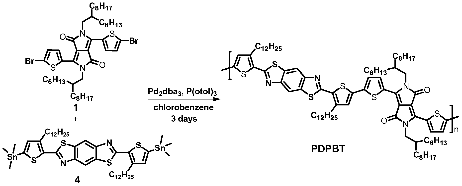
Synthesis of 2, 6-Bis( 5-trimethyltin-3-dodecylthiophen-2-yl)benzo[l,2-d;4, 5-dJ- Bisthiazole (4): The distannyl compound 4 was prepared as reported in the literature (Ahmed et al, Macromolecules 2011, 44, 7207-7219).
Synthesis ofPoly[3,6-dithiene-2-yl-2,5-di(2-hexyldecyl)-pyrrolof3,4-cJpyrrole-l,4- dione-5 5''-diyl- -2,5-bis(3-dodecy hiophen-2yl)-benzofl,2-d;4,5-d'Jbisthi zole
(PDPBT): The dibromo compound 1 (380 mg, 0.42 mmol), and di-tin compound 4 (428 mg, 0.42 mmol) and catalyst tris(dibenzylideneacetone)dipalladium (0) (8 mg, 0.008 mmol) and tri-o-tolylphosphine (10 mg, 0.017 mmol) in anhydrous chlorobenzene (20 mL) were heated at reflux for 30 hours. Then the heating was reduced to 50° C; the reaction mixture was poured into 200 mL of methanol containing 5 mL of hydrochloric acid and stirred for 5 hours. The black precipitate was collected via filtration, and was further purified by Soxhlet extraction with methanol and hexane. Then the residue was extracted with chloroform, evaporated and dried to yield a dark brown solid (520 mg, 86%). GPC: Mn = 18.5 Kg/mol, PDI = 3.6; 1H NMR (CDC13, δ ppm): 9.11- 8.72 (m, 2H), 7.61-8.51 (m, 2H), 6.90-7.50 (m, 4H), 3.90-4.10 (m, 4H), 2.60-3.10 (m, 4H), 0.82-1.91 (m, 108H).
The thermal behavior of PDPBT copolymer was investigated by differential scanning calorimetry (DSC) and thermogravimetric analysis (TGA). This copolymer showed onset thermal decomposition temperature above 383 C and no melting transition in DSC up to 300
°C, suggesting that there was no substantial effect in morphology and structural order in the solid state.
PDPBT was soluble in chloroform solution at room temperature and soluble in chlorobenzene and dichlorobenzene at 100 C. The absorption maximum in solution in dilute CHCI3 (~10~6M) was found to be 668 and 723 nm. The absorption spectrum of the thin films was red shifted and showed a broad absorption maximum at 673 and 743 nm. The optical band gap measured at the absorption edge of the film was calculated to be 1.33 eV. The HOMO level of PDPBT was estimated from cyclic voltammetry (CV) results. The onset oxidation and reduction potential was 0.91 V and -0.92 V (versus SCE), from which the HOMO and LUMO level of the polymer were calculated to be 5.31 eV and 3.48 eV, respectively. The electrochemical band gap of the polymer PDPBT was 1.83 eV.
To investigate the morphology of the copolymer PDPBT, X-ray diffractions (XRD) were performed on polymer thin films. No lamellar reflections or peak was observed indicating the amorphous nature of PDPBT thin films.
Example 6 - Transistors and Solar Cells Comprising PDPBT
Transistors based on PDPBT were fabricated and tested with conventional top-contact and bottom-gate geometry on top of silicon (gate) and silicon dioxide (dielectric, tox=200-300 nm) substrates and patterned gold source/drain electrodes. The channel widths of the devices were 400-1000 μιη and lengths were 20-100 μιη. The surface of the silicon dioxide was cleaned and treated with octyltrichlorosilane (OTS8). Polymer solutions were spun onto a substrate. Thin films were then annealed at 200 °C for 10 min under inert atmosphere.
Devices were tested in nitrogen-filled dry box. Electrical parameters were calculated by using the standard equation for metal-oxide-semiconductor field-effect transistors in saturation region: Ids=^C0W/2L)(Vg-Vt) . The typical output and transfer characteristics of PDPBT OFETs are shown in Figure 24a and 24b. PDPBT showed p-channel characteristics with a large current modulation (Wloff >105). The average threshold voltage (Vt) of PDPBT was - 14.0 V. PDPBT had an average hole mobility of 0.0052 cm /Vs. Compared to the transistor comprising PDPBT, which in some embodiments serves as a comparable example, the hole mobility of transistors comprising PDPTT or PDPTTOx is substantially higher.
Solar cells using PDPBT as donor and PC71BM as acceptor components were fabricated. The active layer of the solar cells were spin-coated from PDPBT:PC7iBM (1 :2 w wt) blend solution in chloroform on top of PEDOT:PSS coated ITO substrates. The solar cell devices were finished by deposition of the cathodes, consisting of 1 nm LiF and 80 nm
Al, in a thermal evaporator. The spin-coating of the active layer was performed in a glove box and the films were annealed at 150°C for 10 min. The solar cells had an active area of 9 mm2.
A power conversion efficiency of 2.72%, with Jsc of 6.79 mA/cm , Voc of 0.79 V, and FF of 0.56, were observed in PDPBT:PC7iBM (1 :2) bulk heterojunction solar cells.
The PDPBT:PC7iBM device showed photoconversion efficiency with a
monochromatic EQE around 30% over the 350-600 wavelength range. The calculated Jsc by integrating the EQE curve of PDPBT:PC7iBM solar cell with an AM1.5G reference spectrum
2 2 was 6.43 mA/cm (in the wavelength range of 350-580 nm) compared with 6.79 mA/cm measured on same size device; thus, the spectral mismatch factor was ~6%>.
MATERIALS AND METHODS
All commercially available reagents were purchased from Sigma-Aldrich, Across , Alfa-Aesar and TCI America Laboratory of chemicals. FT-IR spectra were obtained from Perkin Elmer 1720 FT-IR spectrophotometer with KBr pellets. Mass spectra were recorded on a Bruker Esquire LC/ Ion Trap Mass spectrometer. 1H-NMR spectra were recorded on a Bruker AV300/AV500 at 300 MHz/500 MHz respectively using CDC13 or C6D4C12 or CF3COOD as the solvents. Gel Permeation Chromatography (GPC) analysis was performed using Polymer Lab Model 120 Gel Permeation Chromatograph (DRI / High Sensitivity Refractive Index Detector and PL-BV400HT Viscometer) against polystyrene standards in chlorobenzene at 60 °C. Thermogravimetric analysis (TGA) analysis was conducted with a TA Instruments Q50 TGA at a heating rate of 10 °C/min under a nitrogen gas flow. Cyclic voltammetry was done on an EG&G Princeton Applied Research Potentiostat/Galvanostat 273 A. A three-electrode cell was used, using platinum wire electrodes as both counter and working electrode. Silver/silver ion (Ag in 0.1 M AgN03 solution, Bioanalytical System, Inc.) was used as a reference electrode. Ferrocene/ferrocenium (Fc/Fc+) was used as an internal standard. The potential values obtained in reference to Ag/Ag+ were converted to the saturated calomel electrode (SCE) scale. Thin film cyclic voltammetry was performed in acetonitrile containing 0.1M TBAPF6. UV-vis absorption spectra were recorded on a Perkin- Elmer model Lambda 900 UV/vis/near-IR spectrophotometer. The photoluminescence (PL) emission spectra were obtained with a Photon Technology International (PTI) Inc. model QM2001-4 spectra fluorimeter. Thin film of polymer was drop-cast on a freshly cleaned glass substrate for X-ray diffraction (XRD). XRD patterns were obtained on a Bruker AXS D8 Focus diffractometer with Cu Ka beam (40 kV, 40 mA; λ = 0.15418 nm).
Claims
1. A polymer comprising a first repeating unit of formula (I)

wherein:
(i) X at each occurrence is independently selected from O, S and Se;
(ii) m is 0, 1 , 2 or 3;
(iii) R1 at each occurrence is independently selected from hydrogen and optionally substituted C1-C30 organic group; R2, R3, R4 and R5 at each occurrence is independently selected from hydrogen, halogen, cyano, and optionally substituted C1-C30 organic group;
(iv) the polymer has a Mw of 40,000 Da or more; and
(v) A is an electron withdrawing group represented by
-* NxY*- or -* Nx N - ? wherein (a) Y at each occurrence is independently selected from O, S, Se and N(R6); and (b) R6 at each occurrence is independently selected from hydrogen and optionally substituted C1-C30 linear, branched or cyclic organic group.
2. The polymer of claim 1 , wherein A is represented

3. The polymer of claim 1 or 2, wherein X is S.
4. The polymer of any of claims 1-3, wherein m is 1.
5. The polymer of any of claims 1-4, wherein R1 at each occurrence is independently selected from hydrogen, optionally substituted alkyl, optionally substituted heteroalkyl, fluoroalkyl, fluoroheteroalkyl; and wherein R2, R3, R4 and R5 at each occurrence is independently selected from hydrogen, halogen, cyano, optionally substituted alkyl, fluoroalkyl, optionally substituted alkoxy, fluoroalkoxy, optionally substituted thioalkyl, fluorothioalkyl, optionally substituted alkyl sulfoxide, fluoroalkyl sulfoxide, optionally substituted alkyl sulfone, and fluoroalkyl sulfone.
6. The polymer of any of claims 1-5, wherein R at each occurrence is independently selected from C4-C30 linear, branched or cyclic alkyl, wherein R at each occurrence is independently C4-C30 linear or branched alkoxy, and wherein R3, R4 and R5 at each occurrence is H.
7. A polymer comprising a first repeating unit of formula (I)

wherein:
(i) X at each occurrence is independently selected from O, S and Se;
(ii) m is 0, 1, 2 or 3;
(iii) R1 at each occurrence is independently selected from hydrogen and optionally substituted C1-C30 organic group; R2, R3, R4 and R5 at each occurrence are independently selected from hydrogen, halogen, cyano, and optionally substituted C1-C30 organic group;
(iv) the polymer has a Mw of 40,000 Da or more; and
(v) A is an electron withdrawing group comprising two or more rings fused together, with two of said rings each comprising at least one imine group.
8. The polymer of claim 7, wherein A comprises at least two thiazole rings.
9. The polymer of claim 7 or 8, wherein A comprises three or more rings fused together.
The olymer of any of claims 7-9, wherein A is selected from

(i) W at each occurrence is independently selected from N and C(R6);
(ii) Y and Z at each occurrence is independently selected from O, S, Se, P(R6), P(0)R6, Si(R6)2, C(R6)2 and N(R6); and
(iii) R6 at each occurrence is independently selected from hydrogen, halogen, hydroxyl, cyano, nitro, silyl, siloxanyl, and optionally substituted C1-C30 linear, branched or cyclic organic group.
11. The olymer of any of claims 7-10, wherein A is selected from

The polymer of any of claims 1-11, wherein the first repeating unit is selected from

13. The polymer of any of claims 1-12, wherein the polymer consists essentially of the first repeating unit.
14. A method for making the polymer of any of claims 1-13, comprising copolymerizing a first compound represented by

wherein:
(i) X at each occurrence is independently selected from O, S and Se;
(ii) m is 0, 1, 2 or 3;
(iii) R1 at each occurrence is independently selected from hydrogen and optionally substituted C1-C30 organic group; R2, R3, R4 and R5 at each occurrence are independently selected from hydrogen, halogen, cyano, and optionally substituted C1-C30 organic group; and
(iv) A is an electron withdrawing group comprising two or more rings fused together, with two of said rings each comprising at least one imine group.
15. A composition comprising the polymer of any of claims 1-13 or made by the method of claim 14.
16. An electronic device comprising the polymer of any of claims 1-13 or made by the method of claim 14, or the composition of claim 15.
17. A p-channel transistor comprising a semiconducting layer, wherein said layer is obtained by solution processing and annealing a composition, and wherein said composition comprises at least one solvent and the polymer of any of claims 1-13 or made by the method of claim 14, and wherein the transistor has a field effect carrier mobility of 0.3 cm /Vs or more.
Applications Claiming Priority (2)
| Application Number | Priority Date | Filing Date | Title |
|---|---|---|---|
| US201261692180P | 2012-08-22 | 2012-08-22 | |
| US61/692,180 | 2012-08-22 |
Publications (1)
| Publication Number | Publication Date |
|---|---|
| WO2014031733A1 true WO2014031733A1 (en) | 2014-02-27 |
Family
ID=49162213
Family Applications (1)
| Application Number | Title | Priority Date | Filing Date |
|---|---|---|---|
| PCT/US2013/055967 Ceased WO2014031733A1 (en) | 2012-08-22 | 2013-08-21 | Diketopyrrolopyrrole polymers for electronics and optoelectronics |
Country Status (1)
| Country | Link |
|---|---|
| WO (1) | WO2014031733A1 (en) |
Cited By (1)
| Publication number | Priority date | Publication date | Assignee | Title |
|---|---|---|---|---|
| WO2017150119A1 (en) * | 2016-02-29 | 2017-09-08 | 富士フイルム株式会社 | Organic semiconductor film, organic semiconductor element, polymer, and organic semiconductor composition |
Citations (3)
| Publication number | Priority date | Publication date | Assignee | Title |
|---|---|---|---|---|
| US20090302311A1 (en) * | 2006-06-30 | 2009-12-10 | Turbiez Mathieu G R | Diketopyrrolopyrrole polymers as organic semiconductors |
| US20110215313A1 (en) * | 2008-10-31 | 2011-09-08 | Basf Se | Diketopyrrolopyrrole polymers for use in organic semiconductor devices |
| US20120186652A1 (en) * | 2010-11-24 | 2012-07-26 | Hualong Pan | Conjugated Polymers and Their Use in Optoelectronic Devices |
-
2013
- 2013-08-21 WO PCT/US2013/055967 patent/WO2014031733A1/en not_active Ceased
Patent Citations (3)
| Publication number | Priority date | Publication date | Assignee | Title |
|---|---|---|---|---|
| US20090302311A1 (en) * | 2006-06-30 | 2009-12-10 | Turbiez Mathieu G R | Diketopyrrolopyrrole polymers as organic semiconductors |
| US20110215313A1 (en) * | 2008-10-31 | 2011-09-08 | Basf Se | Diketopyrrolopyrrole polymers for use in organic semiconductor devices |
| US20120186652A1 (en) * | 2010-11-24 | 2012-07-26 | Hualong Pan | Conjugated Polymers and Their Use in Optoelectronic Devices |
Non-Patent Citations (2)
| Title |
|---|
| JAE WOONG JUNG ET AL: "A high mobility conjugated polymer based on dithienothiophene and diketopyrrolopyrrole for organic photovoltaics", ENERGY & ENVIRONMENTAL SCIENCE, vol. 5, no. 5, 1 January 2012 (2012-01-01), pages 6857, XP055082921, ISSN: 1754-5692, DOI: 10.1039/c2ee21149a * |
| SELVAM SUBRAMANIYAN ET AL: "High Mobility Thiazole-Diketopyrrolopyrrole Copolymer Semiconductors for High Performance Field-Effect Transistors and Photovoltaic Devices", MACROMOLECULES, vol. 45, no. 22, 5 November 2012 (2012-11-05), pages 9029 - 9037, XP055082910, ISSN: 0024-9297, DOI: 10.1021/ma301660j * |
Cited By (2)
| Publication number | Priority date | Publication date | Assignee | Title |
|---|---|---|---|---|
| WO2017150119A1 (en) * | 2016-02-29 | 2017-09-08 | 富士フイルム株式会社 | Organic semiconductor film, organic semiconductor element, polymer, and organic semiconductor composition |
| JPWO2017150119A1 (en) * | 2016-02-29 | 2018-11-29 | 富士フイルム株式会社 | Organic semiconductor film, organic semiconductor element, polymer, and organic semiconductor composition |
Similar Documents
| Publication | Publication Date | Title |
|---|---|---|
| Shi et al. | Imide-functionalized thiazole-based polymer semiconductors: Synthesis, structure–property correlations, charge carrier polarity, and thin-film transistor performance | |
| US8871884B2 (en) | Copolymer semiconductors comprising thiazolothiazole or benzobisthiazole, or benzobisoxazole electron acceptor subunits, and electron donor subunits, and their uses in transistors and solar cells | |
| Guo et al. | Naphthalene diimide-based polymer semiconductors: synthesis, structure–property correlations, and n-channel and ambipolar field-effect transistors | |
| Yuen et al. | Strong acceptors in donor–acceptor polymers for high performance thin film transistors | |
| Sonar et al. | High mobility organic thin film transistor and efficient photovoltaic devices using versatile donor–acceptor polymer semiconductor by molecular design | |
| Hwang et al. | n-type naphthalene diimide–biselenophene copolymer for all-polymer bulk heterojunction solar cells | |
| CN102640316B (en) | P-type materials and organic electronic devices | |
| Zhan et al. | Copolymers of perylene diimide with dithienothiophene and dithienopyrrole as electron-transport materials for all-polymer solar cells and field-effect transistors | |
| Shao et al. | A water-soluble polythiophene for organic field-effect transistors | |
| Fei et al. | Conjugated copolymers of vinylene flanked naphthalene diimide | |
| US9809594B2 (en) | Non-fullerene electron acceptors for organic photovoltaic devices | |
| Shi et al. | Naphtho [1, 2-b: 5, 6-b′] dithiophene-based donor–acceptor copolymer semiconductors for high-mobility field-effect transistors and efficient polymer solar cells | |
| Hwang et al. | New thienothiadiazole-based conjugated copolymers for electronics and optoelectronics | |
| Tsai et al. | New two-dimensional thiophene− acceptor conjugated copolymers for field effect transistor and photovoltaic cell applications | |
| US7495251B2 (en) | Electronic devices containing acene-thiophene copolymers with silylethynyl groups | |
| Cheng et al. | A diketopyrrolopyrrole–thiazolothiazole copolymer for high performance organic field-effect transistors | |
| He et al. | Poly (3, 6-dihexyl-thieno [3, 2-b] thiophene vinylene): Synthesis, field-effect transistors, and photovoltaic properties | |
| US9296864B2 (en) | Polymer material for highly efficient organic thin-film solar cell, and organic thin-film solar cell using same | |
| TWI534173B (en) | Fused random bithiophene-ethylene copolymer | |
| Wang et al. | Dual Imide-Functionalized Unit-Based Regioregular D–A1–D–A2 Polymers for Efficient Unipolar n-Channel Organic Transistors and All-Polymer Solar Cells | |
| Shi et al. | Bichalcogenophene imide-based homopolymers: chalcogen-atom effects on the optoelectronic property and device performance in organic thin-film transistors | |
| Shi et al. | Synthesis of copolymers based on thiazolothiazole and their applications in polymer solar cells | |
| Murali et al. | Narrow band gap conjugated polymer for improving the photovoltaic performance of P3HT: PCBM ternary blend bulk heterojunction solar cells | |
| Subramaniyan et al. | Thiazolothiazole donor–acceptor conjugated polymer semiconductors for photovoltaic applications | |
| Li et al. | Poly (2, 5-bis (2-octyldodecyl)-3, 6-di (furan-2-yl)-2, 5-dihydro-pyrrolo [3, 4-c] pyrrole-1, 4-dione-co-thieno [3, 2-b] thiophene): a high performance polymer semiconductor for both organic thin film transistors and organic photovoltaics |
Legal Events
| Date | Code | Title | Description |
|---|---|---|---|
| 121 | Ep: the epo has been informed by wipo that ep was designated in this application |
Ref document number: 13760152 Country of ref document: EP Kind code of ref document: A1 |
|
| NENP | Non-entry into the national phase |
Ref country code: DE |
|
| 122 | Ep: pct application non-entry in european phase |
Ref document number: 13760152 Country of ref document: EP Kind code of ref document: A1 |