WO2014018372A1 - Method for producing nickel-containing films - Google Patents
Method for producing nickel-containing films Download PDFInfo
- Publication number
- WO2014018372A1 WO2014018372A1 PCT/US2013/051094 US2013051094W WO2014018372A1 WO 2014018372 A1 WO2014018372 A1 WO 2014018372A1 US 2013051094 W US2013051094 W US 2013051094W WO 2014018372 A1 WO2014018372 A1 WO 2014018372A1
- Authority
- WO
- WIPO (PCT)
- Prior art keywords
- substrate
- nickel
- substrate surface
- consisting essentially
- precursor
- Prior art date
- Legal status (The legal status is an assumption and is not a legal conclusion. Google has not performed a legal analysis and makes no representation as to the accuracy of the status listed.)
- Ceased
Links
Classifications
-
- C—CHEMISTRY; METALLURGY
- C23—COATING METALLIC MATERIAL; COATING MATERIAL WITH METALLIC MATERIAL; CHEMICAL SURFACE TREATMENT; DIFFUSION TREATMENT OF METALLIC MATERIAL; COATING BY VACUUM EVAPORATION, BY SPUTTERING, BY ION IMPLANTATION OR BY CHEMICAL VAPOUR DEPOSITION, IN GENERAL; INHIBITING CORROSION OF METALLIC MATERIAL OR INCRUSTATION IN GENERAL
- C23C—COATING METALLIC MATERIAL; COATING MATERIAL WITH METALLIC MATERIAL; SURFACE TREATMENT OF METALLIC MATERIAL BY DIFFUSION INTO THE SURFACE, BY CHEMICAL CONVERSION OR SUBSTITUTION; COATING BY VACUUM EVAPORATION, BY SPUTTERING, BY ION IMPLANTATION OR BY CHEMICAL VAPOUR DEPOSITION, IN GENERAL
- C23C16/00—Chemical coating by decomposition of gaseous compounds, without leaving reaction products of surface material in the coating, i.e. chemical vapour deposition [CVD] processes
- C23C16/06—Chemical coating by decomposition of gaseous compounds, without leaving reaction products of surface material in the coating, i.e. chemical vapour deposition [CVD] processes characterised by the deposition of metallic material
- C23C16/18—Chemical coating by decomposition of gaseous compounds, without leaving reaction products of surface material in the coating, i.e. chemical vapour deposition [CVD] processes characterised by the deposition of metallic material from metallo-organic compounds
-
- C—CHEMISTRY; METALLURGY
- C07—ORGANIC CHEMISTRY
- C07F—ACYCLIC, CARBOCYCLIC OR HETEROCYCLIC COMPOUNDS CONTAINING ELEMENTS OTHER THAN CARBON, HYDROGEN, HALOGEN, OXYGEN, NITROGEN, SULFUR, SELENIUM OR TELLURIUM
- C07F17/00—Metallocenes
Definitions
- the present invention relates generally to methods of depositing thin films of metal.
- the invention relates to the use of coordination complexes containing nickel to deposit films consisting essentially of nickel.
- ALD atomic layer deposition
- Ni(PF 3 ) 4 is toxic and bis(cyclopentadienyl)Ni can lead to carbon contamination in the film.
- the present invention addresses these problems by providing novel chemistries.
- the method comprises: providing a substrate surface; exposing the substrate surface to a vapor comprising a precursor having a structure represented by:
- R 1 is t-butyl and each R 2 is each independently any C1-C3 alkyl group; exposing the substrate to a reducing gas to provide a film consisting essentially of nickel on the substrate surface.
- Embodiment two includes a modification to the method of embodiment one, wherein R 2 is methyl.
- Embodiment three includes a modification to the method of embodiment one, wherein R 2 is C2 or C3 alkyl.
- Embodiment four includes a modification to the method of any of embodiments one through three, wherein the precursor is homoleptic.
- Embodiment five includes a modification to the method of any of embodiments one through four, wherein the substrate comprises silicon.
- Embodiment six includes a modification to the method of any of embodiments one through five, wherein the substrate surface is exposed to the precursor and reductant gas substantially simultaneously or sequentially.
- Embodiment seven includes a modification to the method of any of embodiments one through six, wherein the reducing gas comprises ammonia gas or hydrogen gas.
- Embodiment eight includes a modification to the method of any of embodiments one through seven, wherein the film consisting essentially of nickel contains no oxygen.
- Embodiment nine is directed to a method of depositing a film consisting essentially of nickel via atomic layer deposition, the method comprising: providing a substrate surface comprising silicon, wherein the substrate surface has a temperature ranging from between about 120 and about 250 °C; sequentially exposing the substrate surface to vapor comprising a precursor having a structure represented by:
- R 1 is t-butyl and each R 2 is each independently any C1-C3 alkyl group; exposing the substrate to a reducing gas to provide a film consisting essentially of nickel on the substrate surface.
- Embodiment ten includes a modification to the method of embodiment nine, wherein R 2 is methyl.
- Embodiment 11 includes a modification to the method of embodiment nine or 10, wherein exposure of the substrate surface to the vapor comprising the precursor and the reducing gas occurs under an oxide-free environment.
- Embodiment 12 includes a modification to the method of any of embodiments nine through 11, wherein the precursor is homoleptic.
- Embodiment 13 includes a modification to the method of any of embodiments nine through 12, wherein the reducing gas comprises ammonia gas or hydrogen gas.
- Embodiment 14 includes a modification to the method of any of embodiments nine through 13, wherein the film consisting essentially of nickel is oxide-free and contains less than about 5% carbon.
- Embodiment 15 is directed to a method of depositing a film consisting essentially of nickel via chemical vapor deposition, the method comprising: providing a substrate surface comprising silicon; simultaneously exposing the substrate surface to a vapor comprising a precursor having a structure represented by:
- R 1 is t-butyl and each R 2 is each independently any C1-C3 alkyl group while exposing the substrate to a reducing gas to provide a film consisting essentially of nickel on the substrate surface.
- Embodiment 16 includes a modification to the method of embodiment
- Embodiment 15 includes a modification to the method of embodiment 15 or 16, wherein exposure of the substrate surface to the vapor comprising the precursor and the reducing gas occurs under an oxide-free environment.
- Embodiment 18 includes a modification to the method of any of embodiments 15 through 17, wherein the precursor is homoleptic.
- Embodiment 19 includes a modification to the method of any of embodiments 15 through 18, wherein the reducing gas comprises ammonia gas or hydrogen gas.
- Embodiment 20 includes a modification to the method of any of embodiments 15 through 19, wherein the film consisting essentially of nickel is oxide free and contains less than about 5% carbon.
- FIG. 1 shows a thermogravimetric analysis of two metal coordination complexes.
- the term "consisting essentially of nickel” means that deposited layer contains mostly elemental nickel. In one or more embodiments, small amounts of impurities are within the meaning of the term. In one or more embodiments, the film contains no oxygen, and/or contains less than 5% carbon.
- metal coordination complex as used herein is used interchangeably with “metal complex” and “coordination complex,” and includes structures that consist of a central metal atom bonded to one or more ligands.
- metal complexes of the invention comprise of pyrrolyl-based ligands coordinated to nickel atoms.
- the metal coordination complex has a structure represented by formula (I):
- R 1 is t-butyl and each R 2 is each independently any C1-C3 alkyl group.
- R 2 is methyl.
- R 2 is C2 or C3 alkyl.
- the precursor is homoleptic.
- the precursors described herein are alternatives to previously used precursors like Ni(PF 3 ) 4 and bis(cyclopentadienyl)nickel.
- the precursors according to formula (I) above are lower toxicity, but cost competitive as compared to Ni(PF 3 ) 4 .
- the precursors are also likely to results in less carbon contamination than previously used bis(cyclopentadienyl)nickel complexes.
- ALD deposition methods of the invention can be evaluated using methods known in the art, allowing selection of appropriate temperature and pressure for the reaction. In general, lower molecular weight and the presence of functional groups result in a melting point that yields liquids at typical delivery temperatures and increased vapor pressure.
- these metal coordination complexes are useful to deposit thin films consisting essentially of nickel.
- another aspect of the invention relates to a method of depositing a film consisting essentially of nickel. The method comprises providing a substrate surface; exposing the substrate surface to a vapor comprising a precursor having a structure represented by formula (I):
- R 1 is t-butyl and each R 2 is each independently any C1-C3 alkyl group; and exposing the substrate to a reducing gas to provide a film consisting essentially of nickel on the substrate surface.
- the precursor may be selected according to any of the embodiments listed above.
- the substrate comprises silicon.
- the substrate surface is exposed to the precursor and reductant gas substantially simultaneously or sequentially. As used herein, "substantially simultaneously" refers to either co-flow or where there is merely overlap between exposures of the precursor and reductant.
- the reducing gas may comprise ammonia or hydrogen gas.
- the reducing gas may comprise ammonia or hydrogen gas.
- the film consisting essentially of nickel contains no nitrogen.
- the films deposited via the methods described herein are suitable for use in the production of low-resistance, nickel silicide contacts because of reduced levels of carbon and/or oxygen contaminants.
- the nickel film Once the nickel film is deposited over a silicon substrate, it can be converted to the silicide form by reaction with a silicon substrate. In one or more embodiments, this may be achieved through annealing at slightly elevated temperatures, if necessary. However, in one or more embodiments, the temperature does not exceed about 250 to about 275 °C, because of the possibility of the formation of the disilicide (NiSi 2 ), which is too electrically resistive. In other embodiments, such as those relating to anti-corrosion coatings, there would not necessarily be this temperature limit.
- the complex chemically decomposes the nickel into the film and produce vapor-phase ligands (or vapor-phase ligand decomposition products).
- Decomposition is achieved both by thermal cleavage of the metal-ligand bond and by contacting the metal complex, or surface -bound ligands, with a reducing gas results in an exchange reaction between the metal coordination complex and the reducing gas, thereby dissociating the bound organic ligand and producing a first layer consisting essentially of nickel on the surface of the substrate.
- the ligands can then be removed, and not incorporated into the film.
- the substrate for deposition of the elemental thin layer films may be any substrate suitable for conformal film coating in an ALD or CVD process.
- substrates include silicon, silica or coated silicon, metal, metal oxide and metal nitride.
- the substrate is a semiconductor substrate.
- exposure of the substrate surface to the vapor comprising the precursor and the reducing gas occurs under an oxide-free environment.
- the deposited film contains no oxygen incorporation (i.e., is oxide-free). Oxide-free films are achievable using the precursors and methods described herein because the ligands do not contain oxygen atoms.
- the above metal coordination complexes can be used in ALD or CVD processes to deposit the films described herein.
- the phrase “atomic layer deposition” is used interchangeably with “ALD,” and refers to a process which involves sequential exposures of chemical reactants, and each reactant is deposited from the other separated in time and space.
- the phrase “atomic layer deposition” is not necessarily limited to reactions in which each reactant layer deposited is limited to a monolayer (i.e., a layer that is one reactant molecule thick).
- Atomic layer deposition is distinguished from “chemical vapor deposition” or “CVD,” in that CVD refers to a process in which one or more reactants continuously form a film on a substrate by reaction in a process chamber containing the substrate or on the surface of the substrate.
- CVD refers to a process in which one or more reactants continuously form a film on a substrate by reaction in a process chamber containing the substrate or on the surface of the substrate.
- Another aspect of the invention relates to a method of depositing a film consisting essentially of nickel via atomic layer deposition.
- the method comprises providing a substrate surface comprising silicon, wherein the substrate surface has a temperature ranging from between about 120 and about 250 °C; sequentially exposing the substrate surface to vapor comprising a precursor having a structure represented by formula (I):
- R 1 is t-butyl and each R 2 is each independently any C1-C3 alkyl group; and exposing the substrate to a reducing gas to provide a film consisting essentially of nickel on the substrate surface.
- a reducing gas to provide a film consisting essentially of nickel on the substrate surface.
- R 2 is methyl.
- the precursor is homoleptic.
- Another aspect of the invention relates to a method of depositing a film consisting essentially of nickel via chemical vapor deposition.
- the method comprises providing a substrate surface comprising silicon; simultaneously exposing the substrate surface to a vapor comprising a precursor having a structure represented by formula (I):
- R 1 is t-butyl and each R 2 is each independently any C1-C3 alkyl group while exposing the substrate to a reducing gas to provide a film consisting essentially of nickel on the substrate surface.
- a reducing gas to provide a film consisting essentially of nickel on the substrate surface.
- any of the above variants in the metal coordination complex may be used.
- R 2 is methyl.
- the precursor is homoleptic.
- a second layer may be formed on the first layer by repeating any of the process reaction cycles described above. Any hydrocarbon remaining from the preceding reduction reaction or decomposition may be purged from the deposition chamber using an inert gas. A metal coordination complex in vapor phase is again flowed into the chamber/exposed to metal film on the substrate surface. An exchange reaction occurs between the metal coordination complex and hydrogen at the metal surface of the first atomic layer. This displaces one of the ligands from the vapor phase metal coordination complex and leaves the metal atom of the metal coordination complex bound to the metal atom of the first atomic layer. The reaction time, temperature and pressure are selected to create a metal-surface interaction and form a layer on the surface of the substrate.
- Unreacted vapor phase metal coordination complex and released ligand can then be purged from the deposition chamber using an insert gas.
- a reducing gas may again be flowed into the deposition chamber to reduce the bond(s) between the metal and any remaining ligand(s), releasing the remaining ligand(s) from the metal center and producing a second atomic layer of elemental metal on the first atomic layer of elemental metal. Additional repetitions of the deposition cycle may be used to build a layer of elemental metal of the desired thickness.
- the substrate surface has a temperature of greater than about 70, 80, 90 or 100 °C and less than about 250, 225, 200 or 175 °C. While not wishing to be bound to any particular theory, it is thought that low temperatures at which the process is able to be carried out prevents carbon incorporation.
- the deposition can be carried out at atmospheric pressure but is more commonly carried out at a reduced pressure.
- the vapor pressure of the metal coordination complex should be high enough to be practical in such applications.
- one or more layers may be formed during a plasma enhanced atomic layer deposition (PEALD) process.
- PEALD plasma enhanced atomic layer deposition
- the use of plasma provides sufficient energy to promote a species into the excited state where surface reactions become favorable and likely.
- Introducing the plasma into the process can be continuous or pulsed.
- sequential pulses of precursors (or reactive gases) and plasma are used to process a layer.
- the reagents may be ionized either locally (i.e., within the processing area) or remotely (i.e., outside the processing area). In some embodiments, remote ionization can occur upstream of the deposition chamber such that ions or other energetic or light emitting species are not in direct contact with the depositing film.
- the plasma is generated external from the processing chamber, such as by a remote plasma generator system.
- the plasma may be generated via any suitable plasma generation process or technique known to those skilled in the art.
- plasma may be generated by one or more of a microwave (MW) frequency generator or a radio frequency (RF) generator.
- MW microwave
- RF radio frequency
- the frequency of the plasma may be tuned depending on the specific reactive species being used. Suitable frequencies include, but are not limited to, 2 MHz, 13.56 MHz, 40 MHz, 60 MHz and 100 MHz.
- plasmas may be used during the deposition processes disclosed herein, it should be noted that plasmas may not required. Indeed, other embodiments relate to deposition processes under very mild conditions without a plasma.
- the substrate is subjected to processing prior to and/or after forming the layer.
- This processing can be performed in the same chamber or in one or more separate processing chambers.
- the substrate is moved from the first chamber to a separate, second chamber for further processing.
- the substrate can be moved directly from the first chamber to the separate processing chamber, or it can be moved from the first chamber to one or more transfer chambers, and then moved to the desired separate processing chamber.
- the processing apparatus may comprise multiple chambers in communication with a transfer station. An apparatus of this sort may be referred to as a "cluster tool" or "clustered system", and the like.
- a cluster tool is a modular system comprising multiple chambers which perform various functions including substrate center-finding and orientation, degassing, annealing, deposition and/or etching.
- a cluster tool includes at least a first chamber and a central transfer chamber.
- the central transfer chamber may house a robot that can shuttle substrates between and among processing chambers and load lock chambers.
- the transfer chamber is typically maintained at a vacuum condition and provides an intermediate stage for shuttling substrates from one chamber to another and/or to a load lock chamber positioned at a front end of the cluster tool.
- processing chambers which may be used include, but are not limited to, cyclical layer deposition (CLD), atomic layer deposition (ALD), chemical vapor deposition (CVD), physical vapor deposition (PVD), etch, pre-clean, chemical clean, thermal treatment such as RTP, plasma nitridation, degas, orientation, hydroxylation and other substrate processes.
- CLD cyclical layer deposition
- ALD atomic layer deposition
- CVD chemical vapor deposition
- PVD physical vapor deposition
- etch pre-clean
- thermal treatment such as RTP, plasma nitridation, degas, orientation, hydroxylation and other substrate processes.
- the substrate is continuously under vacuum or "load lock” conditions, and is not exposed to ambient air when being moved from one chamber to the next.
- the transfer chambers are thus under vacuum and are “pumped down” under vacuum pressure.
- Inert gases may be present in the processing chambers or the transfer chambers.
- an inert gas is used as a purge gas to remove some or all of the reactants after forming the silicon layer on the surface of the substrate.
- the deposited films are oxide-free.
- deposition occurs without a break in vacuum and/or without exposure to ambient conditions, thereby preventing exposure (and thus incorporation) of oxygen.
- a purge gas is injected at the exit of the deposition chamber to prevent reactants from moving from the deposition chamber to the transfer chamber and/or additional processing chamber.
- the flow of inert gas forms a curtain at the exit of the chamber.
- the substrate can be processed in single substrate deposition chambers, where a single substrate is loaded, processed and unloaded before another substrate is processed.
- the substrate can also be processed in a continuous manner, like a conveyer system, in which multiple substrate are individually loaded into a first part of the chamber, move through the chamber and are unloaded from a second part of the chamber.
- the shape of the chamber and associated conveyer system can form a straight path or curved path.
- the processing chamber may be a carousel in which multiple substrates are moved about a central axis and are exposed to deposition, etch, annealing, cleaning, etc. processes throughout the carousel path.
- the substrate can be heated or cooled. Such heating or cooling can be accomplished by any suitable means including, but not limited to, changing the temperature of the substrate support and flowing heated or cooled gases to the substrate surface.
- the substrate support includes a heater/cooler which can be controlled to change the substrate temperature conductively.
- the gases (either reactive gases or inert gases) being employed are heated or cooled to locally change the substrate temperature.
- a heater/cooler is positioned within the chamber adjacent the substrate surface to convectively change the substrate temperature.
- the substrate can also be stationary or rotated during processing. A rotating substrate can be rotated continuously or in discreet steps.
- a substrate may be rotated throughout the entire process, or the substrate can be rotated by a small amount between exposure to different reactive or purge gases. Rotating the substrate during processing (either continuously or in steps) may help produce a more uniform deposition or etch by minimizing the effect of, for example, local variability in gas flow geometries.
- Figure 1 shows the thermogravimetric analysis of two metal coordination complexes.
- One coordination complex contains a nickel atom with two cyclopentadienyl ligands that contain four methyl groups each ((Me 8 Cp) 2 Ni).
- the other complex contains a nickel atom with two Cp* ligands ((Me 10 Cp) 2 Ni).
- the weight of the sample material for each complex was measured as the material was exposed to increasing temperature. As the temperature is increased, the complexes evaporate, which decreases the measured weight.
- Figure 1 shows both the weight of the material as a function of time as well as the first derivative of the weight.
Landscapes
- Chemical & Material Sciences (AREA)
- Organic Chemistry (AREA)
- General Chemical & Material Sciences (AREA)
- Chemical Kinetics & Catalysis (AREA)
- Engineering & Computer Science (AREA)
- Materials Engineering (AREA)
- Mechanical Engineering (AREA)
- Metallurgy (AREA)
- Chemical Vapour Deposition (AREA)
Description
METHODS FOR PRODUCING NICKEL-CONTAINING FILMS
TECHNICAL FIELD
[0001] The present invention relates generally to methods of depositing thin films of metal. In particular, the invention relates to the use of coordination complexes containing nickel to deposit films consisting essentially of nickel.
BACKGROUND
[0002] Deposition of thin films on a substrate surface is an important process in a variety of industries including semiconductor processing, diffusion barrier coatings and dielectrics for magnetic read/write heads. In the semiconductor industry, in particular, miniaturization requires atomic level control of thin film deposition to produce conformal coatings on high aspect structures. One method for deposition of thin films chemical vapor deposition (CVD). In this process, a wafer is typically exposed to one or more volatile precursors, which react to deposit a films. A related process is atomic layer deposition (ALD), which employs sequential surface reactions to form layers of precise thickness controlled at the Angstrom or monolayer level. Most ALD processes are based on binary reaction sequences which deposit a binary compound film. Because the surface reactions are sequential, the two gas phase reactants are not in contact, and possible gas phase reactions that may form and deposit particles are limited. [0003] There is a need for new deposition chemistries that are commercially viable, particularly in the area of elemental metal films, including nickel films for nickel silicide contacts. For example, nickel films have been deposited using Ni(PF3)4 and bis(cyclopentadienyl)Ni coordination complexes. However, each of these complexes has presented problems. Ni(PF3)4 is toxic and bis(cyclopentadienyl)Ni can lead to carbon contamination in the film. The present invention addresses these problems by providing novel chemistries.
SUMMARY
[0004] Aspects of the invention are directed to methods of depositing a film consisting essentially of nickel. Various embodiments are listed below. It will be understood that the embodiments listed below may be combined not only as listed
below, but in other suitable combinations in accordance with the scope of the invention.
[0005] In embodiment one, the method comprises: providing a substrate surface; exposing the substrate surface to a vapor comprising a precursor having a structure represented by:

[0006] Embodiment two includes a modification to the method of embodiment one, wherein R2 is methyl. Embodiment three includes a modification to the method of embodiment one, wherein R2 is C2 or C3 alkyl. Embodiment four includes a modification to the method of any of embodiments one through three, wherein the precursor is homoleptic. Embodiment five includes a modification to the method of any of embodiments one through four, wherein the substrate comprises silicon. Embodiment six includes a modification to the method of any of embodiments one through five, wherein the substrate surface is exposed to the precursor and reductant gas substantially simultaneously or sequentially. Embodiment seven includes a modification to the method of any of embodiments one through six, wherein the reducing gas comprises ammonia gas or hydrogen gas. Embodiment eight includes a modification to the method of any of embodiments one through seven, wherein the film consisting essentially of nickel contains no oxygen.
[0007] Embodiment nine is directed to a method of depositing a film consisting essentially of nickel via atomic layer deposition, the method comprising: providing a substrate surface comprising silicon, wherein the substrate surface has a temperature ranging from between about 120 and about 250 °C; sequentially exposing the substrate surface to vapor comprising a precursor having a structure represented by:

[0008] Embodiment ten includes a modification to the method of embodiment nine, wherein R2 is methyl. Embodiment 11 includes a modification to the method of embodiment nine or 10, wherein exposure of the substrate surface to the vapor comprising the precursor and the reducing gas occurs under an oxide-free environment. Embodiment 12 includes a modification to the method of any of embodiments nine through 11, wherein the precursor is homoleptic. Embodiment 13 includes a modification to the method of any of embodiments nine through 12, wherein the reducing gas comprises ammonia gas or hydrogen gas. Embodiment 14 includes a modification to the method of any of embodiments nine through 13, wherein the film consisting essentially of nickel is oxide-free and contains less than about 5% carbon.
[0009] Embodiment 15 is directed to a method of depositing a film consisting essentially of nickel via chemical vapor deposition, the method comprising: providing
a substrate surface comprising silicon; simultaneously exposing the substrate surface to a vapor comprising a precursor having a structure represented by:

[0010] Embodiment 16 includes a modification to the method of embodiment
15, wherein R2 is methyl. Embodiment 17 includes a modification to the method of embodiment 15 or 16, wherein exposure of the substrate surface to the vapor comprising the precursor and the reducing gas occurs under an oxide-free environment. Embodiment 18 includes a modification to the method of any of embodiments 15 through 17, wherein the precursor is homoleptic. Embodiment 19 includes a modification to the method of any of embodiments 15 through 18, wherein the reducing gas comprises ammonia gas or hydrogen gas. Embodiment 20 includes a modification to the method of any of embodiments 15 through 19, wherein the film consisting essentially of nickel is oxide free and contains less than about 5% carbon.
BRIEF DESCRIPTION OF THE DRAWINGS
[0011] FIG. 1 shows a thermogravimetric analysis of two metal coordination complexes.
DETAILED DESCRIPTION
[0012] Before describing several exemplary embodiments of the invention, it is to be understood that the invention is not limited to the details of construction or process steps set forth in the following description. The invention is capable of other embodiments and of being practiced or being carried out in various ways. It is also to be understood that the complexes and ligands of the present invention may be illustrated herein using structural formulas which have a particular stereochemistry. These illustrations are intended as examples only and are not to be construed as limiting the disclosed structure to any particular stereochemistry. Rather, the illustrated structures are intended to encompass all such complexes and ligands having the indicated chemical formula.
[0013] As used herein, the term "consisting essentially of nickel" means that deposited layer contains mostly elemental nickel. In one or more embodiments, small amounts of impurities are within the meaning of the term. In one or more embodiments, the film contains no oxygen, and/or contains less than 5% carbon.
[0014] The term "metal coordination complex" as used herein is used interchangeably with "metal complex" and "coordination complex," and includes structures that consist of a central metal atom bonded to one or more ligands. As will be discussed in more detail below, the metal complexes of the invention comprise of pyrrolyl-based ligands coordinated to nickel atoms.
[0015] One aspect of the invention relates to such a metal coordination complex. The metal coordination complex has a structure represented by formula (I):
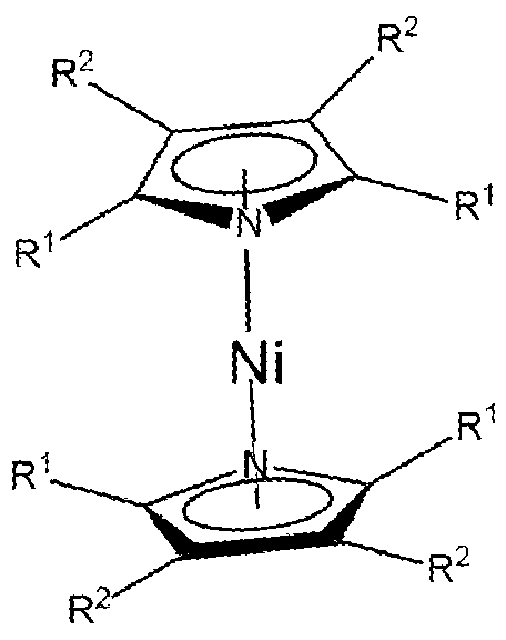
[0016] The precursors described herein are alternatives to previously used precursors like Ni(PF3)4 and bis(cyclopentadienyl)nickel. The precursors according to formula (I) above are lower toxicity, but cost competitive as compared to Ni(PF3)4. The precursors are also likely to results in less carbon contamination than previously used bis(cyclopentadienyl)nickel complexes.
[0017] The synthesis of this metal coordination complex begins with the production of the pyrrole-based ligand according to known methods in the art. The pyrrole-based ligand is then treated with butyllithium to form the pyrrolide, which is then reacted with a nickel halide to form the bis(pyrrolyl)nickel precursor. An exemplary synthesis scheme is shown below as Schematic 1 :
Schematic 1:

[0018] The properties of a specific metal coordination complex for use in the
ALD deposition methods of the invention can be evaluated using methods known in
the art, allowing selection of appropriate temperature and pressure for the reaction. In general, lower molecular weight and the presence of functional groups result in a melting point that yields liquids at typical delivery temperatures and increased vapor pressure.
[0019] In one or more embodiments, these metal coordination complexes are useful to deposit thin films consisting essentially of nickel. Thus, another aspect of the invention relates to a method of depositing a film consisting essentially of nickel. The method comprises providing a substrate surface; exposing the substrate surface to a vapor comprising a precursor having a structure represented by formula (I):

wherein R1 is t-butyl and each R2 is each independently any C1-C3 alkyl group; and exposing the substrate to a reducing gas to provide a film consisting essentially of nickel on the substrate surface. The precursor may be selected according to any of the embodiments listed above. In one or more embodiments, the substrate comprises silicon. In one or more embodiments, the substrate surface is exposed to the precursor and reductant gas substantially simultaneously or sequentially. As used herein, "substantially simultaneously" refers to either co-flow or where there is merely overlap between exposures of the precursor and reductant. The reducing gas may comprise ammonia or hydrogen gas. The reducing gas may comprise ammonia or hydrogen gas. In a particular embodiment, the film consisting essentially of nickel contains no nitrogen.
[0020] In one or more embodiments, the films deposited via the methods described herein are suitable for use in the production of low-resistance, nickel silicide contacts because of reduced levels of carbon and/or oxygen contaminants. Once the nickel film is deposited over a silicon substrate, it can be converted to the
silicide form by reaction with a silicon substrate. In one or more embodiments, this may be achieved through annealing at slightly elevated temperatures, if necessary. However, in one or more embodiments, the temperature does not exceed about 250 to about 275 °C, because of the possibility of the formation of the disilicide (NiSi2), which is too electrically resistive. In other embodiments, such as those relating to anti-corrosion coatings, there would not necessarily be this temperature limit.
[0021] While not wishing to be bound to any particular theory, it is thought that when the substrate is exposed to the complex, the complex chemically decomposes the nickel into the film and produce vapor-phase ligands (or vapor-phase ligand decomposition products). Decomposition is achieved both by thermal cleavage of the metal-ligand bond and by contacting the metal complex, or surface -bound ligands, with a reducing gas results in an exchange reaction between the metal coordination complex and the reducing gas, thereby dissociating the bound organic ligand and producing a first layer consisting essentially of nickel on the surface of the substrate. The ligands can then be removed, and not incorporated into the film.
[0022] The substrate for deposition of the elemental thin layer films may be any substrate suitable for conformal film coating in an ALD or CVD process. Such substrates include silicon, silica or coated silicon, metal, metal oxide and metal nitride. In one aspect of the invention, the substrate is a semiconductor substrate.
[0023] In one or more embodiments, exposure of the substrate surface to the vapor comprising the precursor and the reducing gas occurs under an oxide-free environment. In further embodiments, the deposited film contains no oxygen incorporation (i.e., is oxide-free). Oxide-free films are achievable using the precursors and methods described herein because the ligands do not contain oxygen atoms.
[0024] The above metal coordination complexes can be used in ALD or CVD processes to deposit the films described herein. As used herein, the phrase "atomic layer deposition" is used interchangeably with "ALD," and refers to a process which involves sequential exposures of chemical reactants, and each reactant is deposited from the other separated in time and space. However, according to one or more embodiments, the phrase "atomic layer deposition" is not necessarily limited to
reactions in which each reactant layer deposited is limited to a monolayer (i.e., a layer that is one reactant molecule thick). Atomic layer deposition is distinguished from "chemical vapor deposition" or "CVD," in that CVD refers to a process in which one or more reactants continuously form a film on a substrate by reaction in a process chamber containing the substrate or on the surface of the substrate.
[0025] Accordingly, another aspect of the invention relates to a method of depositing a film consisting essentially of nickel via atomic layer deposition. The method comprises providing a substrate surface comprising silicon, wherein the substrate surface has a temperature ranging from between about 120 and about 250 °C; sequentially exposing the substrate surface to vapor comprising a precursor having a structure represented by formula (I):

wherein R1 is t-butyl and each R2 is each independently any C1-C3 alkyl group; and exposing the substrate to a reducing gas to provide a film consisting essentially of nickel on the substrate surface. Any of the above variants in the metal coordination complex may be used. For example, in one embodiment, R2 is methyl. In another embodiment, the precursor is homoleptic.
[0026] Another aspect of the invention relates to a method of depositing a film consisting essentially of nickel via chemical vapor deposition. The method comprises providing a substrate surface comprising silicon; simultaneously exposing the substrate surface to a vapor comprising a precursor having a structure represented by formula (I):

[0027] Optionally, a second layer may be formed on the first layer by repeating any of the process reaction cycles described above. Any hydrocarbon remaining from the preceding reduction reaction or decomposition may be purged from the deposition chamber using an inert gas. A metal coordination complex in vapor phase is again flowed into the chamber/exposed to metal film on the substrate surface. An exchange reaction occurs between the metal coordination complex and hydrogen at the metal surface of the first atomic layer. This displaces one of the ligands from the vapor phase metal coordination complex and leaves the metal atom of the metal coordination complex bound to the metal atom of the first atomic layer. The reaction time, temperature and pressure are selected to create a metal-surface interaction and form a layer on the surface of the substrate. Unreacted vapor phase metal coordination complex and released ligand can then be purged from the deposition chamber using an insert gas. A reducing gas may again be flowed into the deposition chamber to reduce the bond(s) between the metal and any remaining ligand(s), releasing the remaining ligand(s) from the metal center and producing a second atomic layer of elemental metal on the first atomic layer of elemental metal. Additional repetitions of the deposition cycle may be used to build a layer of elemental metal of the desired thickness.
[0028] In one or more embodiments, the substrate surface has a temperature of greater than about 70, 80, 90 or 100 °C and less than about 250, 225, 200 or 175 °C. While not wishing to be bound to any particular theory, it is thought that low temperatures at which the process is able to be carried out prevents carbon incorporation.
[0029] The deposition can be carried out at atmospheric pressure but is more commonly carried out at a reduced pressure. The vapor pressure of the metal coordination complex should be high enough to be practical in such applications.
[0030] In some embodiments, one or more layers may be formed during a plasma enhanced atomic layer deposition (PEALD) process. In some processes, the use of plasma provides sufficient energy to promote a species into the excited state where surface reactions become favorable and likely. Introducing the plasma into the process can be continuous or pulsed. In some embodiments, sequential pulses of precursors (or reactive gases) and plasma are used to process a layer. In some embodiments, the reagents may be ionized either locally (i.e., within the processing area) or remotely (i.e., outside the processing area). In some embodiments, remote ionization can occur upstream of the deposition chamber such that ions or other energetic or light emitting species are not in direct contact with the depositing film. In some PEALD processes, the plasma is generated external from the processing chamber, such as by a remote plasma generator system. The plasma may be generated via any suitable plasma generation process or technique known to those skilled in the art. For example, plasma may be generated by one or more of a microwave (MW) frequency generator or a radio frequency (RF) generator. The frequency of the plasma may be tuned depending on the specific reactive species being used. Suitable frequencies include, but are not limited to, 2 MHz, 13.56 MHz, 40 MHz, 60 MHz and 100 MHz. Although plasmas may be used during the deposition processes disclosed herein, it should be noted that plasmas may not required. Indeed, other embodiments relate to deposition processes under very mild conditions without a plasma.
[0031] According to one or more embodiments, the substrate is subjected to processing prior to and/or after forming the layer. This processing can be performed in the same chamber or in one or more separate processing chambers. In some
embodiments, the substrate is moved from the first chamber to a separate, second chamber for further processing. The substrate can be moved directly from the first chamber to the separate processing chamber, or it can be moved from the first chamber to one or more transfer chambers, and then moved to the desired separate processing chamber. Accordingly, the processing apparatus may comprise multiple chambers in communication with a transfer station. An apparatus of this sort may be referred to as a "cluster tool" or "clustered system", and the like.
[0032] Generally, a cluster tool is a modular system comprising multiple chambers which perform various functions including substrate center-finding and orientation, degassing, annealing, deposition and/or etching. According to one or more embodiments, a cluster tool includes at least a first chamber and a central transfer chamber. The central transfer chamber may house a robot that can shuttle substrates between and among processing chambers and load lock chambers. The transfer chamber is typically maintained at a vacuum condition and provides an intermediate stage for shuttling substrates from one chamber to another and/or to a load lock chamber positioned at a front end of the cluster tool. Two well-known cluster tools which may be adapted for the present invention are the Centura® and the Endura®, both available from Applied Materials, Inc., of Santa Clara, Calif. The details of one such staged-vacuum substrate processing apparatus is disclosed in U.S. Pat. No. 5,186,718, entitled "Staged- Vacuum Wafer Processing Apparatus and Method," Tepman et al., issued on Feb. 16, 1993. However, the exact arrangement and combination of chambers may be altered for purposes of performing specific steps of a process as described herein. Other processing chambers which may be used include, but are not limited to, cyclical layer deposition (CLD), atomic layer deposition (ALD), chemical vapor deposition (CVD), physical vapor deposition (PVD), etch, pre-clean, chemical clean, thermal treatment such as RTP, plasma nitridation, degas, orientation, hydroxylation and other substrate processes. By carrying out processes in a chamber on a cluster tool, surface contamination of the substrate with atmospheric impurities can be avoided without oxidation prior to depositing a subsequent film.
[0033] According to one or more embodiments, the substrate is continuously under vacuum or "load lock" conditions, and is not exposed to ambient air when
being moved from one chamber to the next. The transfer chambers are thus under vacuum and are "pumped down" under vacuum pressure. Inert gases may be present in the processing chambers or the transfer chambers. In some embodiments, an inert gas is used as a purge gas to remove some or all of the reactants after forming the silicon layer on the surface of the substrate.
[0034] As discussed above, in some embodiments, the deposited films are oxide-free. In further embodiments, deposition occurs without a break in vacuum and/or without exposure to ambient conditions, thereby preventing exposure (and thus incorporation) of oxygen.
[0035] According to one or more embodiments, a purge gas is injected at the exit of the deposition chamber to prevent reactants from moving from the deposition chamber to the transfer chamber and/or additional processing chamber. Thus, the flow of inert gas forms a curtain at the exit of the chamber.
[0036] The substrate can be processed in single substrate deposition chambers, where a single substrate is loaded, processed and unloaded before another substrate is processed. The substrate can also be processed in a continuous manner, like a conveyer system, in which multiple substrate are individually loaded into a first part of the chamber, move through the chamber and are unloaded from a second part of the chamber. The shape of the chamber and associated conveyer system can form a straight path or curved path. Additionally, the processing chamber may be a carousel in which multiple substrates are moved about a central axis and are exposed to deposition, etch, annealing, cleaning, etc. processes throughout the carousel path.
[0037] During processing, the substrate can be heated or cooled. Such heating or cooling can be accomplished by any suitable means including, but not limited to, changing the temperature of the substrate support and flowing heated or cooled gases to the substrate surface. In some embodiments, the substrate support includes a heater/cooler which can be controlled to change the substrate temperature conductively. In one or more embodiments, the gases (either reactive gases or inert gases) being employed are heated or cooled to locally change the substrate temperature. In some embodiments, a heater/cooler is positioned within the chamber adjacent the substrate surface to convectively change the substrate temperature.
[0038] The substrate can also be stationary or rotated during processing. A rotating substrate can be rotated continuously or in discreet steps. For example, a substrate may be rotated throughout the entire process, or the substrate can be rotated by a small amount between exposure to different reactive or purge gases. Rotating the substrate during processing (either continuously or in steps) may help produce a more uniform deposition or etch by minimizing the effect of, for example, local variability in gas flow geometries.
EXAMPLE
[0039] Figure 1 shows the thermogravimetric analysis of two metal coordination complexes. One coordination complex contains a nickel atom with two cyclopentadienyl ligands that contain four methyl groups each ((Me8Cp)2Ni). The other complex contains a nickel atom with two Cp* ligands ((Me10Cp)2Ni). The weight of the sample material for each complex was measured as the material was exposed to increasing temperature. As the temperature is increased, the complexes evaporate, which decreases the measured weight. Figure 1 shows both the weight of the material as a function of time as well as the first derivative of the weight.
[0040] As can be seen from the data, the (MeioCp^Ni material decreased simply with increasing temperature, indicating that with increasing temperature, the complex evaporated. On the other hand, the ((MesCp^Ni complex shows a more complex pathway, indicating that the complex decomposes to a certain extent. Indeed, the weight of the sample never reaches zero, showing that decomposed material remains.
[0041] This relatively clean vaporization of (MeloCp)2Ni compared to (MesCp^Ni demonstrates that a lack of symmetry in the ligand introduces instability. It is thought that this type of instability contributes to contamination, particularly that of carbon, into the film. For example, with the ligand in (MesCp^Ni, it is thought that the hydrogen on the unsubstituted carbon in the Cp ring is removed, such that the ligand decomposes to non-volatile species and carbon is available to be incorporated in to the film.
[0042] This concept can be extended to the coordination complexes of formula (I). Instead of the unsubstituted carbon in (MesCp^Ni, there is a nitrogen, thereby removing the pathway for decomposition. This therefore allows in asymmetry in the ligand without substantial carbon contamination.
[0043] Reference throughout this specification to "one embodiment," "certain embodiments," "one or more embodiments" or "an embodiment" means that a particular feature, structure, material, or characteristic described in connection with the embodiment is included in at least one embodiment of the invention. Thus, the appearances of the phrases such as "in one or more embodiments," "in certain embodiments," "in one embodiment" or "in an embodiment" in various places throughout this specification are not necessarily referring to the same embodiment of the invention. Furthermore, the particular features, structures, materials, or characteristics may be combined in any suitable manner in one or more embodiments.
[0044] Although the invention herein has been described with reference to particular embodiments, it is to be understood that these embodiments are merely illustrative of the principles and applications of the present invention. It will be apparent to those skilled in the art that various modifications and variations can be made to the method and apparatus of the present invention without departing from the spirit and scope of the invention. Thus, it is intended that the present invention include modifications and variations that are within the scope of the appended claims and their equivalents.
Claims
> claimed is:
A method of depositing a film consisting essentially of nickel, the method comprising:
providing a substrate surface;
exposing the substrate surface to a vapor comprising a precursor having a structure represented by:

exposing the substrate to a reducing gas to provide a film consisting essentially of nickel on the substrate surface.
The method of claim 1, wherein R2 is methyl.
The method of claim 1 , wherein R2 is C2 or C3 alkyl.
The method of any of claims 1-3, wherein the precursor is homoleptic.
The method of any of claims 1-4, wherein the substrate comprises silicon. The method of any of claims 1-5, further comprising reacting the film consisting essentially of nickel with the substrate comprising silicon to form nickel silicide.
The method of any of claims 1-6, wherein the substrate surface is exposed to the precursor and reductant gas substantially simultaneously or sequentially.
 The method of any of claims 1-7, wherein the reducing gas comprises
ammonia gas or hydrogen gas.
9. The method of any of claims 1-8, wherein the film consisting essentially of nickel contains no oxygen.
10. A method of depositing a film consisting essentially of nickel via atomic layer deposition, the method comprising:
providing a substrate surface comprising silicon, wherein the substrate surface has a temperature ranging from between about 120 and about 250 °C;
sequentially exposing the substrate surface to vapor comprising a precursor having a structure represented by:

exposing the substrate to a reducing gas to provide a film consisting essentially of nickel on the substrate surface.
11. The method of claim 10, wherein R2 is methyl.
12. The method of claim 10 or 11, wherein exposure of the substrate surface to the vapor comprising the precursor and the reducing gas occurs under an oxide- free environment.
13. The method of any of claims 1-12, wherein the precursor is homoleptic.
14. The method of any of claims 1-13, wherein the reducing gas comprises
ammonia gas or hydrogen gas.
15. The method of any of claims 1-14, wherein the film consisting essentially of nickel is oxide-free and contains less than about 5% carbon.
Applications Claiming Priority (2)
| Application Number | Priority Date | Filing Date | Title |
|---|---|---|---|
| US13/555,832 US8859045B2 (en) | 2012-07-23 | 2012-07-23 | Method for producing nickel-containing films |
| US13/555,832 | 2012-07-23 |
Publications (1)
| Publication Number | Publication Date |
|---|---|
| WO2014018372A1 true WO2014018372A1 (en) | 2014-01-30 |
Family
ID=49946753
Family Applications (1)
| Application Number | Title | Priority Date | Filing Date |
|---|---|---|---|
| PCT/US2013/051094 Ceased WO2014018372A1 (en) | 2012-07-23 | 2013-07-18 | Method for producing nickel-containing films |
Country Status (3)
| Country | Link |
|---|---|
| US (1) | US8859045B2 (en) |
| TW (1) | TWI527823B (en) |
| WO (1) | WO2014018372A1 (en) |
Cited By (2)
| Publication number | Priority date | Publication date | Assignee | Title |
|---|---|---|---|---|
| WO2019078195A1 (en) * | 2017-10-19 | 2019-04-25 | 株式会社村田製作所 | Cyclopentadienyl nickel complex compound |
| WO2024195914A1 (en) * | 2023-03-17 | 2024-09-26 | (주)후성 | Method for preparing bis(methylcyclopentadienyl)nickel, and nickel oxide thin film using same |
Families Citing this family (1)
| Publication number | Priority date | Publication date | Assignee | Title |
|---|---|---|---|---|
| CN116497231B (en) * | 2023-06-21 | 2024-01-05 | 核工业理化工程研究院 | Method for preparing nickel from tetra (trifluorophosphine) nickel |
Citations (5)
| Publication number | Priority date | Publication date | Assignee | Title |
|---|---|---|---|---|
| US20030129308A1 (en) * | 2001-11-16 | 2003-07-10 | Applied Materials, Inc. | Atomic layer deposition of copper using a reducing gas and non-fluorinated copper precursors |
| US20100092667A1 (en) * | 2002-11-15 | 2010-04-15 | President And Fellows Of Harvard College | Atomic layer deposition using metal amidinates |
| US20110048954A1 (en) * | 2009-09-03 | 2011-03-03 | U.S. Government As Represented By The Secretary Of The Army | Enhanced solderability using a substantially pure nickel layer deposited by physical vapor deposition |
| US8017184B2 (en) * | 2005-06-28 | 2011-09-13 | Micron Technology, Inc. | β-diketiminate ligand sources and metal-containing compounds thereof, and systems and methods including same |
| US20110263100A1 (en) * | 2006-11-02 | 2011-10-27 | Advanced Technology Materials, Inc. | Antimony and germanium complexes useful for cvd/ald of metal thin films |
Family Cites Families (10)
| Publication number | Priority date | Publication date | Assignee | Title |
|---|---|---|---|---|
| US5387315A (en) | 1992-10-27 | 1995-02-07 | Micron Technology, Inc. | Process for deposition and etching of copper in multi-layer structures |
| US6184403B1 (en) | 1999-05-19 | 2001-02-06 | Research Foundation Of State University Of New York | MOCVD precursors based on organometalloid ligands |
| US6998153B2 (en) | 2003-01-27 | 2006-02-14 | Applied Materials, Inc. | Suppression of NiSi2 formation in a nickel salicide process using a pre-silicide nitrogen plasma |
| US7619093B2 (en) * | 2004-10-15 | 2009-11-17 | Praxair Technology, Inc. | Organometallic compounds and mixtures thereof |
| US20070054487A1 (en) | 2005-09-06 | 2007-03-08 | Applied Materials, Inc. | Atomic layer deposition processes for ruthenium materials |
| US20080248648A1 (en) * | 2007-04-06 | 2008-10-09 | Thompson David M | Deposition precursors for semiconductor applications |
| JP5461390B2 (en) | 2007-05-21 | 2014-04-02 | レール・リキード−ソシエテ・アノニム・プール・レテュード・エ・レクスプロワタシオン・デ・プロセデ・ジョルジュ・クロード | New metal precursors for semiconductor applications |
| WO2009086263A1 (en) | 2007-12-28 | 2009-07-09 | Sigma-Aldrich Co. | Methods for preparing thin films using substituted pyrrolyl-metal precursors |
| US7964490B2 (en) | 2008-12-31 | 2011-06-21 | Intel Corporation | Methods of forming nickel sulfide film on a semiconductor device |
| US8592606B2 (en) | 2009-12-07 | 2013-11-26 | Air Products And Chemicals, Inc. | Liquid precursor for depositing group 4 metal containing films |
-
2012
- 2012-07-23 US US13/555,832 patent/US8859045B2/en active Active
-
2013
- 2013-07-17 TW TW102125601A patent/TWI527823B/en active
- 2013-07-18 WO PCT/US2013/051094 patent/WO2014018372A1/en not_active Ceased
Patent Citations (5)
| Publication number | Priority date | Publication date | Assignee | Title |
|---|---|---|---|---|
| US20030129308A1 (en) * | 2001-11-16 | 2003-07-10 | Applied Materials, Inc. | Atomic layer deposition of copper using a reducing gas and non-fluorinated copper precursors |
| US20100092667A1 (en) * | 2002-11-15 | 2010-04-15 | President And Fellows Of Harvard College | Atomic layer deposition using metal amidinates |
| US8017184B2 (en) * | 2005-06-28 | 2011-09-13 | Micron Technology, Inc. | β-diketiminate ligand sources and metal-containing compounds thereof, and systems and methods including same |
| US20110263100A1 (en) * | 2006-11-02 | 2011-10-27 | Advanced Technology Materials, Inc. | Antimony and germanium complexes useful for cvd/ald of metal thin films |
| US20110048954A1 (en) * | 2009-09-03 | 2011-03-03 | U.S. Government As Represented By The Secretary Of The Army | Enhanced solderability using a substantially pure nickel layer deposited by physical vapor deposition |
Cited By (3)
| Publication number | Priority date | Publication date | Assignee | Title |
|---|---|---|---|---|
| WO2019078195A1 (en) * | 2017-10-19 | 2019-04-25 | 株式会社村田製作所 | Cyclopentadienyl nickel complex compound |
| US11332487B2 (en) | 2017-10-19 | 2022-05-17 | Murata Manufacturing Co., Ltd. | Cyclopentadienyl nickel complex compound |
| WO2024195914A1 (en) * | 2023-03-17 | 2024-09-26 | (주)후성 | Method for preparing bis(methylcyclopentadienyl)nickel, and nickel oxide thin film using same |
Also Published As
| Publication number | Publication date |
|---|---|
| US20140023785A1 (en) | 2014-01-23 |
| TWI527823B (en) | 2016-04-01 |
| US8859045B2 (en) | 2014-10-14 |
| TW201412757A (en) | 2014-04-01 |
Similar Documents
| Publication | Publication Date | Title |
|---|---|---|
| US10297462B2 (en) | Methods of etching films comprising transition metals | |
| US9194040B2 (en) | Methods for producing nickel-containing films | |
| US20150162214A1 (en) | Methods Of Selective Layer Deposition | |
| US10233547B2 (en) | Methods of etching films with reduced surface roughness | |
| TW201504468A (en) | Methods of depositing a metal alloy film | |
| US9382270B2 (en) | Substituted silacyclopropane precursors and their use for the deposition of silicon-containing films | |
| US9328415B2 (en) | Methods for the deposition of manganese-containing films using diazabutadiene-based precursors | |
| US9683287B2 (en) | Deposition of films comprising aluminum alloys with high aluminum content | |
| US8859045B2 (en) | Method for producing nickel-containing films | |
| US9236467B2 (en) | Atomic layer deposition of hafnium or zirconium alloy films | |
| US10364492B2 (en) | Film deposition using precursors containing amidoimine ligands |
Legal Events
| Date | Code | Title | Description |
|---|---|---|---|
| 121 | Ep: the epo has been informed by wipo that ep was designated in this application |
Ref document number: 13822698 Country of ref document: EP Kind code of ref document: A1 |
|
| NENP | Non-entry into the national phase |
Ref country code: DE |
|
| 122 | Ep: pct application non-entry in european phase |
Ref document number: 13822698 Country of ref document: EP Kind code of ref document: A1 |