WO2014018303A1 - Multi-tap iq imbalance estimation and correction circuit and method - Google Patents
Multi-tap iq imbalance estimation and correction circuit and method Download PDFInfo
- Publication number
- WO2014018303A1 WO2014018303A1 PCT/US2013/050603 US2013050603W WO2014018303A1 WO 2014018303 A1 WO2014018303 A1 WO 2014018303A1 US 2013050603 W US2013050603 W US 2013050603W WO 2014018303 A1 WO2014018303 A1 WO 2014018303A1
- Authority
- WO
- WIPO (PCT)
- Prior art keywords
- phase
- signal
- mismatch
- signals
- gain
- Prior art date
- Legal status (The legal status is an assumption and is not a legal conclusion. Google has not performed a legal analysis and makes no representation as to the accuracy of the status listed.)
- Ceased
Links
Classifications
-
- H—ELECTRICITY
- H03—ELECTRONIC CIRCUITRY
- H03D—DEMODULATION OR TRANSFERENCE OF MODULATION FROM ONE CARRIER TO ANOTHER
- H03D3/00—Demodulation of angle-, frequency- or phase- modulated oscillations
- H03D3/007—Demodulation of angle-, frequency- or phase- modulated oscillations by converting the oscillations into two quadrature related signals
- H03D3/009—Compensating quadrature phase or amplitude imbalances
-
- H—ELECTRICITY
- H04—ELECTRIC COMMUNICATION TECHNIQUE
- H04L—TRANSMISSION OF DIGITAL INFORMATION, e.g. TELEGRAPHIC COMMUNICATION
- H04L27/00—Modulated-carrier systems
- H04L27/0014—Carrier regulation
- H04L2027/0016—Stabilisation of local oscillators
Definitions
- This relates generally to correction, over a range of signal frequencies, of mismatch between in-phase "I” signals and quadrature-phase “Q” signals of an "IQ signal pair". More particularly, the invention relates to circuitry and a method for correcting arbitrary mismatches, i.e., "IQ mismatches", between an in-phase signal path or "I path” and a quadrature-phase signal path or "Q path” through which the IQ signal pair propagates.
- IQ mismatch is a primary reason for the well-known infeasibility of building multicarrier radio receivers with zero IF (intermediate frequency). Zero IF receivers also are known as "direct conversion receivers".
- the known IQ mismatch correction algorithms do not function properly for frequency-dependent IQ mismatches.
- IQ mismatch also is a concern in other systems that employ quadrature mixing such as superheterdyne receivers employing IQ techniques for image rejection.
- IQ systems are used in digital pre-distortion systems for improving PA (power amplifier) linearity.
- a conventional zero IF receiver 1 includes a low noise amplifier (LNA) 2 which amplifies an RF input signal RF IN and applies the amplified result to the input of a saw filter 3.
- the output of saw filter 3 is applied to both one input of a mixer 5 A and one input of a mixer 5B.
- the other input of mixer 5 A is coupled to receive an in-phase signal generated on conductor 9 A by a phase shifting circuit 9.
- the other input of mixer 5B is coupled to receive a quadrature-phase signal generated on conductor 9B by phase shifting circuit 9.
- a local oscillator 7 generates a signal that is applied to the input of a buffer 8, the output of which is applied to the input of phase shifter 9.
- the quadrature-phase signal generated on conductor 9B is shifted in phase by 90° with respect to the in-phase signal on conductor 9 A.
- LPF low pass filter
- the output of LPF 1 1 A is applied to the input of a buffer 12 A, the output of which is applied by means of a conductor 13A to the input of an ADC 14 A.
- the digital output ⁇ of ADC 14A is generated on a bus 15 A.
- the output of mixer 5B is applied to the input of an amplifier 10B, the output of which is applied to the input of a LPF 1 IB.
- the output of LPF 1 IB is applied to the input of a buffer 12B, the output of which is applied by means of a conductor 13B to the input of an ADC 14B.
- the digital output QOUT of ADC 14B is generated on a bus 15B.
- the signals ⁇ and QOUT constitute an IQ signal pair.
- the signal path including mixer 5 A, amplifier 10A, LPF 1 1A, buffer 12 A, and
- ADC 14A is referred to as an "in-phase path” or “I path” because mixer 5 A receives the in-phase signal 9A generated by phase shifter 9.
- the signal path including mixer 5B, amplifier 10B, LPF 1 IB, buffer 12B, and ADC 14B is referred to as a "quadrature-phase path” or “Q path” because mixer 5B receives a quadrature -phase signal (shifted by 90°) generated on conductor 9B by phase shifter 9.
- I om LPF (cos( co c t)( A cos ⁇ ( co c + co m ) ⁇ + B cos[( co c - co m )t] ;
- I ADC _ OUT y cos ( ⁇ m nTs ) +— cos( co m nTs ) ;
- Q OUT LPF (s ( (o c t)( A cos ⁇ ( a> c + ⁇ ⁇ ) ⁇ + £ cos[( « c - co m )t] ;
- Message signals A and B can be separated as indicated in Equations 6 and 7, wherein the j operator imparts a phase shift of 90°.
- IADC_OUT + A cos ( ⁇ m nTs ;
- FIG. 2 shows the spectrum of the RF input signal RFi N , the demodulated in-phase signal ⁇ , and the demodulated quadrature-phase signal QOUT shown in FIG. 1.
- co c +co m and co c -co m there are two signals, co c +co m and co c -co m .
- co c is the frequency of the carrier signal of the input signal RFI .
- co m is the frequency of the modulation signal, which is the signal of interest.
- the message signal or amplitude signal A corresponds to positive frequencies in the frequency domain spectrum of FIG. 2 and the signal B represents the negative frequencies therein.
- the mixing or demodulation of a positive frequency signal of magnitude A and a negative frequency signal of magnitude B appears in the frequency spectrum of the two signals on the horizontal axes in FIG. 2.
- the in-phase component of the positive frequency may be represented by the vector 27 in FIG. 3.
- the in-phase component ⁇ appears along the x axis and the quadrature-phase component QOUT appears along the y axis in the vector diagrams.
- the signal Iresultant has a positive frequency and that the quadrature component 26,27 is rotated 90° in the clockwise direction, and for a negative frequency signal the quadrature component 26,27 rotates 90° in the counterclockwise direction.
- the positive frequency signal A is of interest, and the negative frequency signal B is to be completely canceled.
- the main components of IQ mismatch include gain error mismatches between the ADCs, mixers, and amplifiers, phase deviation from 90° for the mixer in the Q path, mismatches in the pole frequencies of the LPFs (low pass filters), mismatches at the instants of time at which sampling occurs, and mismatches in the bandwidths of the ADCs.
- Such mismatches may cause generation of image tones.
- Mismatches in the instants of sampling and in the bandwidths of the two ADCs cause phase shift errors. For example, if the instant of sampling in the Q path is not exactly the same as the instant of the corresponding sampling in the I path, this causes a phase shift mismatch which may be problematic.
- Equation 12 the gain mismatch estimate ⁇ corrects for gain mismatch, and the phase mismatch estimate ⁇ corrects for the phase mismatch.
- Equation 12 indicates a conventional way for single-tap imbalance estimation and correction algorithm circuit 32 to achieve single tap estimation and correction of the gain term of the IQ mismatch if ⁇ and ⁇ are constant over the frequency band of interest.
- the signal QOUT is multiplied by a fraction (1+ ⁇ ), and the term ⁇ of the term ⁇ is adjusted so as to make ⁇ equal to zero. That is, the gain ⁇ of the Q path is increased or decreased slightly so as to correct a mismatch in the Q path.
- the vector or phasor analysis previously indicated in FIG. 3 indicates the conventional way for single-tap imbalance estimation and correction algorithm circuit 32 to correct for the phase mismatch ⁇ .
- the I path and the Q path signals should be exactly 90° out of phase, and in effect, the vectors indicated are rotated so as to bring the I path signal and the Q path signal back to being exactly 90° out of phase.
- FIG. 4A illustrates an implementation of a conventional single-tap IQ imbalance estimation and correction system which is a common single-tap prior art system that does not included any frequency dependent estimation/correction, pictorially illustrates a basic way of implementing Equation 12.
- ⁇ is an estimate of the phase mismatch
- ⁇ is an estimate of the gain mismatch.
- Blocks 21-1 and 21-6 represent the sources of the in-phase signal I and the quadrature-phase signal I, respectively.
- a summation ⁇ IQ is performed in block 21-2, using Equation 11.
- ⁇ is multiplied by I in block 21-4 and then is added in block 21-7 to Q.
- ⁇ The value of ⁇ is obtained from Equation 10, using blocks 21-11 and 21-10 to obtain A 2 .
- Blocks 21-3, 21-9, and 21-11 generate ⁇ I 2 - ⁇ Q 2 of equation 10, and that quantity needs to be divided by A 2 to obtain ⁇ .
- Block 21-10 performs that division to generate ⁇ , which then is multiplied by Q, aunt block 21-8 generates the corrected quadrature -phase signal on conductor 15B.
- the main drawback of a single tap correction is the inability to estimate and correct frequency dependent mismatches. Mismatches in the low pass filters in the in-phase path and the quadrature-phase path result in frequency dependent gain and delay mismatches. A single tap correction will fail to correct such mismatches.
- the present invention provides a system (55-1) for correcting gain imbalance and phase imbalance between first ( ⁇ ) and second (QOU T ) signals which are 90° out of phase, including circuitry (32) for estimating the phase mismatch ( ⁇ ) and gain mismatch ( ⁇ ) between the first signal and the second signal signals in a plurality of frequency bands.
- An inverse fast Fourier transform is performed on each of a number of arrays of the phase mismatch estimates and the gain mismatch estimates to generate correction filter coefficients (h[N]) for a N tap correction filter (61).
- the N tap correction filter filters an uncorrected value of the second signal to generate a corrected value of the second signal.
- the invention provides a system (55-1 ) for correcting gain imbalance and phase imbalance between first ( ⁇ ) and second (QOU T ) signals which are 90° out of phase, including circuitry (32) for estimating the phase mismatch ( ⁇ ) and gain mismatch ( ⁇ ) between the first signal ( ⁇ ) and the second signal (QOU T ) signals in a plurality of frequency bands.
- Circuitry (60) performs an inverse fast Fourier transform (IFFT) on each of a number of arrays of the phase mismatch estimates ( ⁇ ) and the gain mismatch estimates ( ⁇ ) to generate correction filter coefficients (h[N]) for a N tap correction filter (61).
- the N tap correction filter (61) filters an uncorrected value of the second signal (QOU T ) to generate a corrected value of the second signal (QOU T ).
- the estimating circuitry (32) performs a function of distinguishing filter delay mismatches and mixer phase mismatches of the first signal ( ⁇ ) and the second signal (QOU T ) signals at the plurality of frequency bands.
- circuitry (40) splits each of the first ( ⁇ ) and (QOU T ) signals into a predetermined number (N) of frequency bands to provide a plurality of in-phase and quadrature-phase signals in the frequency bands, respectively.
- the splitting circuitry (40) includes a bank (40) of filters for splitting each of the first ( ⁇ ) and (QOUT) signals into the predetermined number (N) of frequency bands.
- the inverse fast Fourier transform performing circuitry performs an inverse fast Fourier transform (IFFT) on each of a number of arrays (Hr[k],Hi[k]) of the phase mismatch estimates ( ⁇ ) and gain mismatch estimates ( ⁇ ) to generate filter coefficients (h[N]) for an N tap filter (61) for filtering an uncorrected value of the second signal (QOUT) to generate a corrected value of the second signal (QOUT).
- IFFT inverse fast Fourier transform
- a DC phase correction circuit (59-1 ,65,68) includes a mixer (65) for mixing the first signal ( ⁇ ) with a DC mismatch adjustment value (Pc[0]) and an adder (68) for adding an output of the mixer (65) to the second signal (QOUT) to generate the uncorrected value of the second signal (QOUT) such that the N tap filter (61) essentially eliminates the gain imbalance and the phase imbalance between the first ( ⁇ ) and second (QOUT) signals across all of the (N) frequency bands.
- phase mismatch estimates ( ⁇ ) are determined in accordance with the e uation
- Ike is a cosine-related in-phase signal in a
- Qk c is a cosine-related quadrature signal in the predetermined frequency band produced by the bank (40) of filters
- Iks is a sine-related in-phase signal in a predetermined frequency band produced by the bank (40) of filters
- Qks is a sine-related quadrature signal in the predetermined frequency band produced by the bank (40) of filters.
- the gain mismatch estimates ( ⁇ ) are determined in accordance with equation
- Ike is a cosine -related in-phase signal in a
- Qk c is a cosine-related quadrature signal in the predetermined frequency band produced by the bank (40) of filters
- Iks is a sine-related in-phase signal in the predetermined frequency band produced by the bank (40) of filters
- Qks is a sine-related quadrature signal in the predetermined frequency band produced by the bank (40) of filters.
- the N tap filter (61) includes a finite impulse response filter (FIR).
- FIR finite impulse response filter
- the bank (40) of filters includes a plurality of mixing and filtering circuits (35,36,37) for mixing the first signal ( ⁇ ) with a plurality of first reference signals (DC,Fc,KFc) and for mixing the second signal (QOUT) with a plurality of second reference signals which are shifted 90° relative to a corresponding first reference signal, respectively, and also includes low pass filtering outputs of the various mixed signals to provide the samples of the in-phase and quadrature-phase signal values (Ikc,Qkc,Iks,Qks) generated by the bank (40) of filters.
- the arrays (H r [k], 3 ⁇ 4[k]) are included in a primary feedback loop also including the bank of filters (40), the estimating circuitry (58), and the fast Fourier transform performing circuitry (60), and the DC mismatch adjustment value (Hi[0],Pc[0]) is provided as an input to a secondary feedback loop including the mixer (65) for mixing the first signal ( ⁇ ) with the DC mismatch adjustment value (Pc[0]) and the adder (68) to generate the uncorrected value of the second signal (QOUT).
- the primary and secondary loops are independent.
- the first signal ( ⁇ ) is an in-phase signal and the second signal (QOUT) is a quadrature-phase signal.
- the invention provides a method for correcting gain imbalance and phase imbalance between first ( ⁇ ) and second (QOUT) signals which are 90° out of phase, the method including estimating the phase mismatch ( ⁇ ) and gain mismatch ( ⁇ ) between the first signal ( ⁇ ) and the second signal (QOUT) signals in a plurality of frequency bands; performing an inverse fast Fourier transform (IFFT) on each of a number of arrays of the phase mismatch estimates ( ⁇ ) and a gain mismatch estimates ( ⁇ ) to generate filter coefficients (h[N]) for an N tap correction filter (61); and filtering an uncorrected value of the second signal (QOUT) by means of the an N tap correction filter (61) to generate a corrected value of the second signal (QOUT).
- IFFT inverse fast Fourier transform
- the method includes distinguishing filter delay mismatch components and mixer phase input mismatch components of the first signal (3 ⁇ 4 ⁇ ) and the second signal (QOUT) signals in the multiple bands of frequencies and using the filter delay mismatch components and mixer phase input mismatch components separately to determine the phase mismatch estimates ( ⁇ ) and the gain mismatch estimates ( ⁇ ).
- the method includes providing each of the first ( ⁇ ) and
- the method includes generating a DC mismatch adjustment value (Pc[0]) on the basis of a phase mismatch estimate ( ⁇ ) at zero frequency, mixing the first signal ( ⁇ ) with the DC mismatch adjustment value (Pc[0]) and an adder (68), and adding an output of a mixer (65) to the second signal (QOUT) to generate a value of the second signal (QOUT) such that the N tap filter (61) essentially eliminates the gain imbalance and the phase imbalance between the first ( ⁇ ) and (QOUT) signals at DC and across all of the (N) frequency bands.
- the method includes determining the phase mismatch estimates ( ⁇ ) in accordance with the e uation
- ⁇ is a phase mismatch estimate
- ⁇ is a gain mismatch estimate
- Ike is a cosine-related in-phase signal in a predetermined frequency band
- (3 ⁇ 4 c is a cosine -related quadrature signal in the predetermined frequency band
- Iks is a sine-related in-phase signal in the
- Qks is a sine -related quadrature signal in the
- the estimating includes computing the gain mismatch and the phase mismatch using discrete Fourier transforms in accordance with the equations
- PhaseMismatch E (Jp ase - Qphase - 90 deg)
- E represents an averaging operation
- k varies from 0 to N
- N represents the number of points in an IFFT
- n represents the sample number
- the invention provides a system for correcting gain imbalance and phase imbalance between first ( ⁇ ) and second (QOU T ) signals which are 90° out of phase, including means (32) for estimating the phase mismatch ( ⁇ ) and gain mismatch ( ⁇ ) between the first signal (IQU T ) and the second signal (QOU T ) signals in a plurality of frequency bands; means (60) for performing an inverse fast Fourier transform (IFFT) on each of a number of arrays of the phase mismatch estimates ( ⁇ ) and a gain mismatch estimates ( ⁇ ) to generate filter coefficients (h[N]) for an N tap correction filter (61); and wherein the N tap correction filter (61) filters an uncorrected value of the second signal (QOU T ) to generate a corrected value of the second signal (QOU T ).
- IFFT inverse fast Fourier transform
- the system includes means (58) for distinguishing filter delay mismatch components and mixer phase mismatch components of the first signal (IOU T ) and the second signal (QOU T ) signals in the multiple bands of frequencies.
- FIG. 1 is a block diagram of conventional zero IF receiver.
- FIG. 2 is a frequency spectrum diagram of the RF input, I path, and Q path signals of the zero if receiver in FIG. 1.
- FIG. 3 is a diagram that shows vectors which are useful in explaining operation of the prior art and the present invention.
- FIG. 4A is a block diagram of a conventional IQ imbalance estimation and correction system.
- FIG. 4B is a block diagram of a multi-tap IQ imbalance estimation and correction system of the present invention.
- FIG. 5A is a block diagram of a filter bank used in accordance with the present invention.
- FIG. 5B is a block diagram which more completely represents each of the various sections 35, 36, and 37 of FIG. 5 A.
- FIG. 6A is a diagram useful in understanding Equations 15-17.
- FIG. 6B is a diagram useful in understanding equations 15-21.
- FIG. 7 is a diagram which is helpful in understanding the derivation of
- FIG. 8 is a block diagram of a partial implementation of the IQ imbalance estimation and correction algorithm in block 32 of FIG. 4B, excluding a DC phase correction.
- FIG. 9 is a block diagram of a complete implementation of the IQ imbalance estimation and correction algorithm in block 32 of FIG. 4B, including a DC phase correction.
- FIGS. 10A and 10B are phasor diagrams are useful in explaining the need for distinguishing mismatches of the mixer signal phases and the filter delay mismatches in an IQ system.
- FIGS. 11 A and 1 IB are phasor diagrams which are useful in explaining filter delay mismatch in an IQ system.
- Multi-tap IQ imbalance estimation and correction systems are described which estimate and corrects for arbitrary phase and gain mismatches between an in-phase signal and a quadrature-phase signal of an IQ signal pair across a frequency range of interest.
- the estimation and correction of IQ mismatch/imbalance is accomplished using a single filter bank and without use of a calibration signal.
- the estimation and correction of IQ mismatch/imbalance is accomplished by using DFT (discrete Fourier transform)/FFT (fast Fourier transform) techniques.
- delay mismatches in the LPF's of a receiver are distinguished from phase mismatches in the mixer inputs to develop estimates of phase mismatch and gain mismatch.
- correction filter coefficients are obtained from mismatch values using inverse FFT techniques.
- I-path filter in-phase path filter
- Q-path filter quadrature-phase path filter
- the multi-tap IQ mismatch estimation and correction algorithm performed in circuit 32 estimates and corrects arbitrary mismatches between the in-phase I-path and the quadrature-phase Q-path without use of a calibration signal or tone, by processing the IQ signal pair passed through a filter bank shown in subsequently described FIG. 5A.
- the multi-tap mismatch estimation and correction algorithm performed by circuit 32 then independently estimates the phase mismatch ⁇ ⁇ and the gain mismatch Af for the I-path and Q-path, at a frequency "f" within each band of interest.
- the estimation and correction algorithm estimates each of the filter coefficients h[N] to be used for a single FIR (finite impulse response) filter that corrects for the IQ imbalances or mismatches for each frequency band of interest.
- filter bank 40 includes a number of mixing and filtering circuits, such as circuits 36, 37, and 38, for splitting the digital in-phase signal 1 ⁇ 2 into separate frequency bands of interest.
- the first mixing and filtering circuit includes a digital mixer that has one input coupled to IIN, and another input generated by a NCO (numerically controlled oscillator).
- NCO 42 is operated to provide a DC output to mixer 41.
- the output of mixer 41 is provided as an input to a 1 MHZ low pass filter and decimation circuit 43 which produces a digital output signal I 0c having a frequency in the range from 0-1 MHZ.
- 5A includes a digital mixer 44 having one input that receives II and another input that receives the output of a NCO 45 having a frequency Fc MHZ.
- the output of mixer 44 is provided as an input to a 1 MHZ low pass filter and decimation circuit 46, which produces a digital output signal Ii c having a frequency in the range from 1-3 MHZ.
- the K filtering circuit 37 of filter bank 40 includes a digital mixer 47 that has one input coupled to I IN and another input that receives the output of a NCO 48 having a frequency KxFc MHZ.
- There are N such filtering circuits having spectrums centered at frequencies of 0, Fc, 2Fc,..,NFc, respectively, where K is any number between 0 and N.
- the K ow pass filter and decimation circuit would produce signals having a spectrum centered at KxFc ⁇ 1MHz.
- the foregoing low pass and decimation circuits 43, 46, and 49 may be substantially identical except that they pass different frequency ranges.
- each of sections 35, 36, 37, etc. in FIG. 5A actually includes a second mixer which receives a second local oscillator signal that is 90° out-of-phase with the first local oscillator signal and also includes a second LPF and decimate circuit which filters the output of the second mixer, as shown in FIG. 5B.
- mixing and filtering circuit 36A in FIG. 5B indicates how each of mixing and filtering circuits 35, 36, and 37 of FIG. 5A may be implemented.
- Mixing and filtering circuit 36A includes mixer 44 and LPF and decimate circuit 46 as in FIG. 5A to generate a digital output signal I kc for the k* band.
- Mixing and filtering circuit 36A also includes a second mixer 44A which receives I IN and a second signal produced by NCO 45 which is exactly 90° out of phase with the signal provided to mixer 44.
- Mixer 44 A generates a digital input to a second LPF and decimate circuit 46A, which generates a second digital output signal I ks for the k th band.
- NCO 45 includes a first section 45A which generates the "cosine" local oscillator output signal to mixer 44, and also includes a 90° phase shifting circuit 45B which generates the "sine" local oscillator output signal to mixer 44A.
- Equations 15 and 18 show the outputs I kc and I ks , wherein the term "LPF" in Equations 15 and 18 means that whatever is inside the brackets/parentheses is part of the low pass filter.
- Equations 16 and 19 show the outputs Qk c and Qk s .
- Each of the filters in bank 40 is used to obtain a separate gain mismatch value A f , a separate phase mismatch term sin((
- N represents the number of frequency bands of interest generated by filter bank 40 in FIG. 5 A. Equations 13 and 14 below are used to derive the expressions used in the estimation portion of the estimation and correction algorithm executed in block 32 of FIG. 4B.
- Equation 13 provides the estimated gain mismatch or imbalance Af between the I path and the Q path, at the frequency "f".
- Equation 14 provides the estimated phase mismatch ⁇ at the particular frequency f.
- Use of the multiple filters in filter bank 40 therefore provides estimates of the gain mismatch A f and phase mismatch ⁇ ⁇ across a desired range of individual frequencies in multiple frequency bands or ranges of interest.
- Each If and Q f represents a corresponding frequency range/band within which a particular representative frequency "f" lies, where f is equal to kFc, and If and Qf are the outputs of K th filter bank and each has bandwidth of KFc ⁇ 1 MHZ.
- the number N of frequency bands required depends on the amount of IQ mismatch between the I signal and the Q signal of the IQ signal pair. For example, an amount of IQ mismatch which causes a larger number of cross frequencies to be generated requires a larger number of frequency bands to be generated by filter bank 40 of FIG. 5 A. However, if the amount of IQ mismatch across the range of frequencies of interest is fairly constant, filter bank 40 may require a relatively low number (for example, only 4 or 8) of mixing and filtering circuits.
- Filter bank 40 of FIG. 5 A may be optimized to reduce the amount of integrated circuit area consistent with the required operating speed of the system in which the IQ signal pair is utilized.
- the input signal 1 ⁇ 2 is mixed with the outputs of the various mixers 41, 45, etc. I IN is unchanged by the first mixer 41, and the output I 0c of the filter and decimate circuit 43 contains signal frequencies from 0 to 1 MHZ.
- the second band generated by mixing and filtering circuit 36 contains signal components of frequencies from 1 to 3 MHZ which are centered at a center frequency f c , and the other signal frequencies of the output of mixer 44 are filtered out by filter and decimate circuit 43.
- the remaining mixing and filtering circuits generate separate similar output signals in separate bands of the input spectrum in generally the same way.
- Equations 15-26 below show the derivation of the IQ phase mismatch estimate ⁇ over a predetermined range of N frequency bands into which I I has been split by filter bank 40 of FIG. 5 A.
- I kc LPF ' (A cos( kco c + ⁇ m )nTs . cos( £i» c nTs + ⁇ ))
- I kc and Q kc are signals generated by filter bank 40
- Ts is the sampling period
- n is the number of samples
- ⁇ is the phase mismatch
- ⁇ may be any arbitrary phase. Note that the number n of samples is different than and unrelated to the number N of filters in filter bank 40. Also note that conventional analog signal sampling is performed at the ADC inputs.
- the outputs of the corresponding LPFs are used. There two LPF output signals for each band, one in response to L N and the other in response to Q IN . There are both an in-phase mixer and a quadrature-phase mixer, an in-phase NCO and a quadrature-phase NCO, and an in-phase LPF and a quadrature-phase LPF in each of mixer/filter circuits 35, 36, and 37.
- )) in Equation 17 is the component of interest because the term sin ( ⁇ ) therein represents the IQ signal pair phase mismatch.
- Equation 17 The first term of Equation 17 should converge to zero, but this will occur only if the modulation frequency co m of L N is zero or close to zero.
- the term (A 2 /8) ⁇ sin ( ⁇ ) of Equation 17 can be used to conveniently determine the estimated phase mismatch ⁇ only if the first term in Equation 17 does converge to zero.
- Equation 17 When co m is zero, the first term in Equation 17 does not converge to zero.
- Equations 18-20 below are similar to Equations 15-17 and show further steps in the derivation of phase mismatch estimate equation 26, which holds even when co m is equal to zero.
- I ks LPF (A cos( ka> c + ⁇ m )nTs . sin( ⁇ nTs + &))
- I kc Q kc + I b Q b sin( ⁇ ) ; where and are signals generated by filter bank 40, Ts is the sampling period, n is the number of samples, ⁇ is the phase mismatch, and ⁇ may be any arbitrary phase.
- Equations 15-21 the subscript “c” in the terms Ike and Qkc indicates “cosine” terms in some of the equations, and the subscript “s” in Ik s and Qks indicates “sine” terms in some of the equations, as illustrated in FIGS. 5 A and 5B.
- FIG. 6A indicates the signal flow digital mixer 50 receiving the in-phase signal I kc of Equation 15 and the quadrature -phase signal Q kc of Equation 16, and also shows the flow of the resulting mixed signal being applied to the input of a digital summer 51.
- the output of digital summer 51 is used in generating the desired phase mismatch estimate ⁇ .
- FIG. 6B shows the signal flow of the output of digital mixer 50 shown in FIG. 6A being applied to one input of a digital adder 52.
- Digital mixer 50A receives the in-phase signal of Equation 18 and the quadrature -phase signal Qk s of Equation 18.
- FIG. 6B also shows the flow of the resulting mixer output signal being applied to the input of a digital summer 51 , the output of which is subsequently used for deriving Equation 26 for the phase mismatch estimate ⁇ .
- Equations 18-21 indicate how to eliminate the first term on the right side of
- Equation 17 which fails to converge to zero under DC conditions, and therefore causes problems in obtaining the phase mismatch estimate ⁇ using the 8 ⁇ ( ⁇ ) term on the right side of Equation 17.
- a second mixer (not shown) receives an input based on the same NCO but with its phase shifted 90°, and provides an output to a second LPF.
- the output of the first LPF is designated I 0c , I lc , or I kc , etc.
- the output of the first LPF is designated I 0s , lis, or I ks , etc.
- the signal generated by the first LPF has a "c" subscript because it is linked to a cosine term in the various equations
- the signal generated by the second LPF has a "s" subscript because it is linked to a sign term in the various equations.
- the foregoing description of the in-phase path is equally applicable to the quadrature-phase path, in which the output of the first LPF is designated Qo c , Qic, or Qk c , etc., and the output of the first LPF is designated Q 0s , Qi s , or Q ks , etc.
- Equation 21 follows from Equations 18 and 19, does not include any terms that fail to converge to zero during the various summations, and is subsequently used to derive Equations 22-25 in order to obtain the phase mismatch estimate Equation 26 shown below.
- Equation 27 is a conventional equation for estimation of the gain mismatch ⁇ between the in-phase and quadrature-phase signals of an IQ signal pair.
- ⁇ I -Q ⁇ — [! + cos ( 2a > m nTs - 2 ⁇ )] - ⁇ [1 - cos( 2co m nTs + 2 ⁇ - 29)]
- Equation 27 The first term on the right side of Equation 27 can be used to determine the gain mismatch ⁇ for a particular band if the second and third terms converge to zero over the summations except for the case when co m is zero or close to zero. If the second and third terms on the right side of Equation 27 do converge to zero over the summations, then the first term allows convenient determination of the gain mismatch estimate ⁇ except at frequencies close to DC. Equations 28-34 below indicate how to achieve cancellation of the second and third terms of Equation 27 except under DC conditions. Equation 28 is employed to cause the second and third terms of Equation 27 to converge to zero, to in effect cancel these terms. Eq. (28):
- ⁇ h e - Q kc ⁇ —[1 - cos( 2w m nTs - 29)] - ⁇ [1 - cos( 2w m nTs +2 ⁇ - 29)]
- N is the number of samples added in the summation.
- FIG. 7 pictorially indicates how the computation of Equation 34 may be implemented in order to obtain the gain mismatch estimate ⁇ .
- the numerator of Equation 34 is the sum of the summation of Ik s 2 and the summation of Ik c 2 minus the summation of Qk s 2 and the summation of (3 ⁇ 4
- the in-phase component I kc indicated in block 51-1 is squared, as indicated in block 51-5, and I ks in block 51-2 is squared as indicated in block 51-6.
- the squared terms in blocks 51-5 and 51-6 are summed as indicated in block 51-9.
- Block 51-11 subtracts the sum of Q ks 2 and Q kc 2 from the sum of I ks 2 and I kc 2 .
- Block 51-12 divides the numerator by the output of adder 51-10, to provide the denominator of Equation 34.
- Divider 51-12 divides the numerator of Equation 34 by its denominator to provide the gain mismatch estimate ⁇ .
- each filter coefficient array h[N] may be obtained by performing an inverse fast Fourier transform (IFFT) of the mismatch function frequency response
- the IFFT of the mismatch function frequency response H[k] provides the filter coefficient array h[N], which may be the same as the filter coefficient array of a FIR filter (finite impulse response filter).
- the filter coefficients of h[N] are obtained by performing an IFFT of the gain term, i.e., the real portion H r [k], of the mismatch function frequency response and the phase term, i.e., the imaginary portion Hi[k] of the mismatch function frequency response.
- the IFFT is performed together on both the gain term and the phase term.
- the real portion H r [k] comes directly from the gain mismatch estimates and is equal to 1+ ⁇ , at a particular frequency.
- the k elements correspond to an array.
- the values of k will be 0,1...7.
- the first element is equal to ⁇ gain mismatch estimate at DC ⁇ + j ⁇ phase mismatch estimate at 0 frequency ⁇ .
- the remaining elements of the filter coefficient array H[0-7] are provided in the same manner, to thereby provide the mismatch function frequency response of the filter.
- the filter coefficient array h[N] may be "windowed” using a conventional windowing function and then used for correcting the gain and phase mismatches between the in-phase and quadrature-phase portions of the IQ signal pair.
- the windowing results in the desired array h[N] of filter coefficients for each of filters 31 and 33 in FIG. 4B.
- the filters h[N] may be infinite impulse response (IIR) filters, depending on the particular implementation, in which cases the IFFT coefficients may be used to provide a IIR filter.
- IQ imbalance estimation and correction system 55 includes ADC 14A which digitizes incoming in-phase analog signal Ii n and also includes ADC 14B which digitizes incoming quadrature -phase analog signal Qi n .
- IQ imbalance estimation and correction system 55 also includes a multi-tap IQ imbalance estimation and correction algorithm system 32A (which corresponds generally to block 32 in FIG. 4B).
- Multi-tap estimation and correction system 32A includes a section 57 which may be utilized to split the digital in-phase and/or quadrature -phase signals into a number N of frequency bands, using filter bank 40 of FIG. 5 A.
- Multi-tap estimation and correction system 32A in FIG. 8 also includes a section 58 which then uses Equation 34 to estimate the gain mismatches ⁇ across the previously mentioned frequency range of interest (i.e., for each band k generated in section 57), in order to generate a "gain mismatch array" G[k].
- Equation 26 is used in section 58 to estimate the phase mismatches across the same frequency range of interest in order to generate a "phase mismatch array" P[k], for each band k.
- Multi-tap estimation and correction system 32A also includes a section 59 which then calculates the above-mentioned real and imaginary coefficient arrays H r [k] and Hi[k] using the gain mismatch arrays G[k] and the phase mismatch arrays P[k], respectively, that are generated in section 58.
- Multi-tap estimation and correction system 32A further includes a section 60 that performs conventional scaling operations on H r [k] and Hi[k] to appropriately scale them, compute the IFFTs, perform a windowing operation, and then compute the IFFTs of the resulting scaled H r [k] and Hi[k] arrays.
- the IFFT output is windowed to obtain the filter coefficient arrays h[N] of the in-phase path filter and the quadrature-phase path filter (e.g., filters 31 and 33 in FIG. 4B, which may be considered to be included in section 58 of FIG. 8).
- the IFFTs provide an N tap FIR filter 61 using the two filter coefficient arrays h[N], where N is the number of mixing and filtering circuits 35, 36, and 37 in filter bank 40 of FIG. 5A.
- the digital in-phase signal ⁇ 0 ⁇ generated on bus 15A by ADC 14A is applied to section 57 of multi-tap estimation and correction system 32A.
- the uncorrected digital quadrature-phase signal Q 0 ui ⁇ UNCORRECTED) generated on bus 15B by ADC 14B is applied to an input of N tap filter 61, which effectively eliminates any phase and/or gain mismatch between the digitized representations 3 ⁇ 4 ⁇ an d Qo (CORRECTED) .
- phase mismatch may be present due to various mismatches between the un-shifted mixer input signals and the 90°-shifted mixer input signals generated by the various LOs (local oscillators) in FIG. 5A.
- This is problematic because IQ phase mismatch can be present at DC from the 90° phase shifter in the LO path in Prior Art FIG. 1. If this is not taken care of, the first band around DC (0-1 MHz in the case shown here) may become unusable.
- Equation 12 To correct for such phase mismatch at DC, the conventional phase mismatch correction previously set forth in Equation 12 may be utilized:
- a value of ⁇ is chosen so that the phase mismatch estimate ⁇ at DC goes to zero in order to correct the phase mismatch at DC.
- ⁇ is generated by ADC 14A, and the signal Qout(DC adjusted) is phase corrected at DC. Note that this phase correction/adjustment is independent of frequency.
- the conventional phase mismatch correction technique based on Equation 12 may be used along with the IQ mismatch corrections at all frequencies, other than DC, which are obtained using the filter coefficient arrays h[N] as previously explained with reference to FIG. 8.
- multi-tap IQ imbalance estimation and correction system 55-1 includes ADC 14A which digitizes incoming in-phase analog signal I; n and also includes ADC 14B which digitizes incoming quadrature-phase analog signal Qi n .
- IQ imbalance estimation and correction system 55-1 also includes a multi-tap IQ imbalance estimation and correction algorithm system 32B.
- Multi-tap estimation and correction system 32B includes section 57 for splitting the digital in-phase and/or quadrature-phase signals into a number N of frequency bands, using filter bank 40 of FIG. 5 A, k being equal to 0,1... N.
- multi-tap estimation and correction system 32B in FIG. 9 also includes section 58, which uses Equation 34 to estimate the gain mismatches ⁇ across the frequency range of interest, except at DC, in order to generate the gain mismatch array G[k].
- Equation 26 is used to estimate the phase mismatches across the same frequency range of interest, including DC, in order to generate a phase mismatch array P[k] for each band k.
- Multi-tap estimation and correction system 32B also includes a section 59-1 which then calculates the above-mentioned real and imaginary coefficient arrays H r [k] and H;[k] using the gain mismatch array G[k] and the phase mismatch array P[k], respectively.
- Section 59-1 also sets a phase correction array Pc[0] equal to the array P[0] at DC frequency, and provides the single DC value Pc[0] on bus 66 to a subsequently described mixer 65, and thereby establishes a "secondary" feedback loop.
- multi-tap estimation and correction system 32B in FIG. 9 also includes section 60 that performs conventional scaling and computing the IFFT of the H r [k] and H;[k] arrays and then performs the conventional windowing operation, in order to obtain the needed filter coefficient arrays h[N].
- the digital in-phase signal ⁇ 0 ⁇ generated on bus 15A by ADC 14A in FIG. 9 is applied to section 57 of multi-tap estimation and correction system 32B.
- the uncorrected digital quadrature-phase signal Qo (UNCORRECTED) generated on bus 15B by ADC 14B is applied to N tap filter 61 , which then effectively eliminates any phase and/or gain mismatch between the digitized representations ⁇ and Qom(CORRECTED) across all frequencies, including DC, of the frequency bands of interest.
- QOU T (CORRECTED) then is fed back as an input to estimation and correction system 32B, which then estimates the gain mismatch ⁇ and phase mismatch ⁇ of the I path in each of the bands, and computes the filter coefficients h[N].
- the path including Qoui(CORRECTED) and multi-tap IQ imbalance estimation and correction system 32 form a "primary" feedback loop. This primary feedback loop continues operating until it determines that the Q path and the I path are precisely matched, at which point the final value of QOU T has been determined. (Alternatively, the roles of IOU T and QOU T in FIG. 8 could be reversed to generate a corrected version of QOU T instead of a corrected version of ⁇ )
- the digital in-phase signal IOU T on bus 15A is applied to section 57 of multi-tap IQ imbalance estimation and correction system 55-1 and also to one input of a digital mixer 65.
- Section 59-1 in FIG. 9 applies a DC correction array component Pc[0], which is set equal to P[0], to another input of mixer 65 via digital bus 66.
- the output of mixer 65 is applied via a digital bus 67 to one input of a digital adder 68, the other input of which receives the uncorrected digital quadrature-phase signal Q 0T J T (UNCORRECTED) generated on bus 15B by ADC 14B.
- the output of adder 68 is applied via digital bus 69 to N tap FIR filter 61, which generates Qo (CORRECTED) on bus 63 and feeds it back as an input to section 57.
- the path including section 59-1, bus 66, digital mixer 65, digital adder 68, N tap filter 61, and section 60 of multi-tap IQ imbalance estimation and correction system 32B form the "secondary" feedback loop, the path including N Filter 61, digital bus 63, and section 57 forming a "primary" feedback loop.
- the correction array element Pc[0] compensates for the phase mismatch under
- the system 55-1 shown in FIG. 9 provides matched in-phase and quadrature -phase signals of an IQ signal pair over any desired frequency range, without requiring a calibration tone.
- the system may be implemented using a single filter bank and a single N tap filter using h[N] as filter coefficients for frequencies other than zero and a separate technique for correcting mismatches at DC to achieve elimination of mismatches over any entire frequency band of interest.
- the correction is entirely digital so there is no need to interface with any RF device or ADC to achieve correction of the IQ imbalance.
- the system and associated algorithm are independent of established radio standards, and allow for integration of the algorithm hardware with the ADCs. Estimates and correction of particular frequency bands can be ignored on the basis of the amount of power in each band. Furthermore, the corrections will hold and not diverge if the power in any band is removed and reapplied.
- phase mismatches of LO local oscillator
- filter delay mismatches both result in significant phase mismatch between the in-phase and quadrature quadrature-phase outputs in an IQ system.
- the phase mismatch can be corrected by imparting a relative phase correction between the in-phase and quadrature-phase outputs.
- the errors resulting from the mismatches of the LO signal phase and the mismatches in filter delay may be analyzed separately.
- the RF input cosine signal is of frequency co c +co m and is down-converted by the local oscillator of frequency co c .
- the local oscillator signal in the quadrature-phase path is the local oscillator signal in the quadrature-phase path.
- FIG. 10A shows the in-phase and quadrature-phase components using a phasor diagram.
- the phasor 73A along the X-axis is the in-phase component I, and also is the reference.
- the ideal quadrature-phase component Q for positive frequency is indicated by phasor 70A, and is oriented 90° counterclockwise relative to the in-phase component 73 A.
- the ideal quadrature-phase component Q for a negative frequency is indicated by phasor 71 A, and is 90° clockwise relative to the in-phase component 73A.
- FIG. 10B illustrates the in-phase and quadrature-phase components for a phase mismatch ⁇ in the LO/mixer signals.
- the phasor 7 IB shows the phasor of the quadrature-phase component Q for negative frequency and phasor 70B shows the phasor for positive frequency.
- the term - ⁇ IQ represents the projection of the quadrature -phase components 70B and 7 IB onto the in-phase component 73B and is equal to sin(O), and is independent of the sign of the frequency.
- FIGS. 10A and 10B therefore indicate estimation of phase mismatches due to filter delay and LO phase mismatch, respectively.
- FIGS. HA and 1 IB indicate a way of estimating the delay mismatches in the filters using Q 2 .
- FIG. 11 A shows a phasor diagram for a delay mismatch in the filters. It can be seen that the projection - ⁇ IQ onto phasor 73 A in FIG. 10A depends on the sign of co in this case. The sign of co is of particular concern as the sign of the correction needs to change depending on the sign of co m .
- Equations 42 and 43 below are based on the IQ signals obtained in Equations 39 and 40, with the amplitude mismatches already corrected by the gain loop, where the gain loop is the real portion of the loop involving the DC component Pc[0] as described with reference to FIG. 9.
- the power output of I + Q for high pass filtering can serve as the cost function for the filter mismatch loop.
- the sign of the phase estimate of the original loop is a function of the sign of the frequency co in presence of filter delay mismatch, and as filtering progresses, a new loop evolves that estimates the filter delay mismatch independently of the sign of the input frequency.
- Estimation of the amplitude and phase mismatches between the in-phase and quadrature-phase paths can be estimated using DFTs (discrete Fourier transforms) and/or FFTs.
- DFTs discrete Fourier transforms
- FFTs discrete Fourier transforms
- a DFT operating on N points sampled uniformly at clock frequency Fs has a "bin resolution" of Fs/2N Hz.
- the need for the previously described filter bank 40 can be avoided, because a FFT computes the amplitude (which may represent the gain) and phase of the in-phase and quadrature-phase signals in each band of bandwidth Fs/2N.
- a large value of N reduces the noise in the estimates of the mismatches but increases the hardware complexity.
- N is chosen such that in a bandwidth of Fs/2N, the amplitude mismatches (and hence the gain mismatches) of the in-phase and quadrature-phase signals are sufficiently constant that the residual mismatch error after correction remains within an acceptable limit in the bandwidth. Equations 45-50 show the computation of the gain mismatches and phase mismatches using DFTs. (Note that DFTs and FFTs provide the same results, although they are implemented differently.)
- PhaseMismatch E ( J P hase ⁇ QP hase ⁇ 90 de ⁇ ) Xi _ imag Xq _ imag
- phase mismatch in Equation 49 corresponds to ⁇ and the term “PhaseMismatch” in Equation 50 corresponds to ⁇ as in earlier equations.
- phase mismatch as used herein may also be used to refer to filter delay mismatches as well as to mismatches in corresponding absolute phase values.
- E in equations 45-50 refers to an "expectation function", which is a mathematical way of referring to average or mean value.
- X represents a frequency domain
- Xi real corresponds to the results of performing a FFT to convert time domain data to frequency domain data.
- IFFT inverse FFT
- phase mismatch ⁇ has to be computed as the average of multiple FFT outputs, ie., as E(Iphase-Qphase-90deg) and not as
- E(Iphase)-E(Qphase)-90deg because E(Iphase) and E(Qphase) tend to zero.
- the same necessity for separating the mismatch components into the LO and filter delay components also applies to the FFT -based approach as well to the DFT -based approach.
- a FFT operating on I 2 and Q 2 can be used to obtain the filter mismatch component of the error.
- an inverse FFT can convert the frequency domain phase and gain mismatch information to an array h[N] of filter coefficients that result in a time domain impulse response of the correction filter, for example as in filter 61 in FIG. 9.
- a rectangular window has a sync response in the frequency domain, resulting in a null at the edge of the filter pass-band, which is undesirable.
- a suitable window such as a Hanning window, is applied to the array h(n) obtained by performing the IFFT.
- the IFFT used is of the standard form
- I out (t) LPF ⁇ RF [N cos( ⁇ c )t ⁇
- a B Q ADC _ OUT (n) — sin(fi ) ml ir - ⁇ + ⁇ ⁇ ⁇ ) -— ⁇ ⁇ ( ⁇ ⁇ 2 ⁇ ⁇ + ⁇ + ⁇ ⁇ 2 ⁇ );
- ⁇ ⁇ ⁇ 2 - ⁇ - ⁇ + ⁇ - AT ⁇ - m2 L ml j
- equations 63 and 64 can be solved for ⁇ and ⁇ .
- An additional advantage in this scheme of correcting the mismatch is that the correction at a frequency can be gated by the power spectrum at the frequency. If the power at a frequency band is observed to be less than a predetermined threshold, we can choose not to adapt the filter coefficients for that band.
- This scheme need not be limited to background estimation and correction, but can be used as one time calibration where the mismatches of a device are determined once and the coefficients are trimmed to remove the mismatch.
- the algorithm can be adapted as a partial background and partial one-time trim.
- the group delay mismatch can be made a one-time calibration and the phase mismatch can be used repeatedly in a background correction algorithm.
Landscapes
- Engineering & Computer Science (AREA)
- Power Engineering (AREA)
- Digital Transmission Methods That Use Modulated Carrier Waves (AREA)
Abstract
A system (55-1) for correcting gain imbalance and phase imbalance between first (Iουτ) and second (QOUT) signals which are 90° out of phase, including circuitry (32) for estimating the phase mismatch (ϕ) and gain mismatch (Δ) between the first signal and the second signal signals in a plurality of frequency bands. An inverse fast Fourier transform is performed on each of a number of arrays of the phase mismatch estimates and the gain mismatch estimates to generate correction filter coefficients (h[N]) for a N tap correction filter (61). The N tap correction filter filters an uncorrected value of the second signal to generate a corrected value of the second signal.
Description
MULTI-TAP IQ IMBALANCE ESTIMATION AND
CORRECTION CIRCUIT AND METHOD
[0001] This relates generally to correction, over a range of signal frequencies, of mismatch between in-phase "I" signals and quadrature-phase "Q" signals of an "IQ signal pair". More particularly, the invention relates to circuitry and a method for correcting arbitrary mismatches, i.e., "IQ mismatches", between an in-phase signal path or "I path" and a quadrature-phase signal path or "Q path" through which the IQ signal pair propagates. BACKGROUND
[0002] IQ mismatch is a primary reason for the well-known infeasibility of building multicarrier radio receivers with zero IF (intermediate frequency). Zero IF receivers also are known as "direct conversion receivers". The known IQ mismatch correction algorithms do not function properly for frequency-dependent IQ mismatches. However, it would be very desirable to have a practical system capable of estimating and correcting for arbitrary mismatches between an I path and a Q path of an IQ signal pair, especially without use of a calibration signal as is required by some existing IQ mismatch correction algorithms, because it is infeasible to add calibration tones at multiple frequencies to determine the mismatch across the multiple frequencies.
[0003] IQ mismatch also is a concern in other systems that employ quadrature mixing such as superheterdyne receivers employing IQ techniques for image rejection. For example, IQ systems are used in digital pre-distortion systems for improving PA (power amplifier) linearity.
[0004] Referring to FIG. 1, a conventional zero IF receiver 1 includes a low noise amplifier (LNA) 2 which amplifies an RF input signal RFIN and applies the amplified result to the input of a saw filter 3. The output of saw filter 3 is applied to both one input of a mixer 5 A and one input of a mixer 5B. The other input of mixer 5 A is coupled to receive an in-phase signal generated on conductor 9 A by a phase shifting circuit 9. The other input of mixer 5B is coupled to receive a quadrature-phase signal generated on conductor 9B by
phase shifting circuit 9. A local oscillator 7 generates a signal that is applied to the input of a buffer 8, the output of which is applied to the input of phase shifter 9. The quadrature-phase signal generated on conductor 9B is shifted in phase by 90° with respect to the in-phase signal on conductor 9 A.
[0005] The output of mixer 5 A is applied to the input of an adjustable gain amplifier
10A, the output of which is applied to the input of a LPF (low pass filter) 1 1A. The output of LPF 1 1 A is applied to the input of a buffer 12 A, the output of which is applied by means of a conductor 13A to the input of an ADC 14 A. The digital output Ιουτ of ADC 14A is generated on a bus 15 A. Similarly, the output of mixer 5B is applied to the input of an amplifier 10B, the output of which is applied to the input of a LPF 1 IB. The output of LPF 1 IB is applied to the input of a buffer 12B, the output of which is applied by means of a conductor 13B to the input of an ADC 14B. The digital output QOUT of ADC 14B is generated on a bus 15B. The signals Ιουτ and QOUT constitute an IQ signal pair.
[0006] The signal path including mixer 5 A, amplifier 10A, LPF 1 1A, buffer 12 A, and
ADC 14A is referred to as an "in-phase path" or "I path" because mixer 5 A receives the in-phase signal 9A generated by phase shifter 9. The signal path including mixer 5B, amplifier 10B, LPF 1 IB, buffer 12B, and ADC 14B is referred to as a "quadrature-phase path" or "Q path" because mixer 5B receives a quadrature -phase signal (shifted by 90°) generated on conductor 9B by phase shifter 9.
[0007] The correction equations for an IQ signal pair are as follows:
Eq.(l): m = A cos[( ων + com )t] + B cos[( (oc - com )t] ;
Eq. (2): Iom = LPF (cos( coct)( A cos {( coc + com )} + B cos[( coc - com )t] ;
A B
Eq. (3) : IADC_OUT = y cos(∞mnTs ) +— cos( comnTs ) ;
Eq. (4) : QOUT = LPF (s ( (oct)( A cos {( a>c + ωη )} + £ cos[( «c - com )t] ; and
Eq. (5): QADC_OUT = ^( (omnTs ) + ^- sin( comnTs ) ; where A is the message signal located at coc+com and B is the message signal located at coc-com, as shown in the upper spectrum plot in FIG. 2 . After being mixed with a local oscillator output signal centered at coc, both of message signals A and B would be located at
com , as shown in the spectrum plots of the in-phase signal Ιουτ and the quadrature-phase signal QOUT in FIG. 2.
[0008] Message signals A and B can be separated as indicated in Equations 6 and 7, wherein the j operator imparts a phase shift of 90°.
Eq. (6): IADC_OUT +
 = A cos(∞mnTs ;
Eq. (7): IADCJOUT ~ JQADC^ = B cos( comnTs ) .
[0009] FIG. 2 shows the spectrum of the RF input signal RFiN, the demodulated in-phase signal Ιουτ, and the demodulated quadrature-phase signal QOUT shown in FIG. 1. In the input spectrum shown in FIG. 2, there are two signals, coc+com and coc-com. coc is the frequency of the carrier signal of the input signal RFI . com is the frequency of the modulation signal, which is the signal of interest. When two RF signals having a carrier frequency coc and a modulation frequency or signal frequency com, respectively, are multiplied or mixed, two signal components are generated, one of which has a frequency coc+com , as shown in FIG. 2. The other signal component has a frequency coc-com.
[0010] In the foregoing equations, the message signal or amplitude signal A corresponds to positive frequencies in the frequency domain spectrum of FIG. 2 and the signal B represents the negative frequencies therein. The mixing or demodulation of a positive frequency signal of magnitude A and a negative frequency signal of magnitude B appears in the frequency spectrum of the two signals on the horizontal axes in FIG. 2. The in-phase component of the positive frequency may be represented by the vector 27 in FIG. 3. The in-phase component Ιουτ appears along the x axis and the quadrature-phase component QOUT appears along the y axis in the vector diagrams. It can be seen that the signal Iresultant has a positive frequency and that the quadrature component 26,27 is rotated 90° in the clockwise direction, and for a negative frequency signal the quadrature component 26,27 rotates 90° in the counterclockwise direction. In this case, only the positive frequencies are of interest. Therefore, the positive frequency signal A is of interest, and the negative frequency signal B is to be completely canceled. Rotating the Q vectors 26,27
counterclockwise by 90° is accomplished by performing a "jQ" operation, wherein the B portion 26 rotates counterclockwise to the left as a result of the I+jQ rotation and completely cancels out the B/2 portion of vector 25. At the same time, vector 27 also rotates
counterclockwise and adds its value A/2 to 2 the A/2 portion of vector 25 to form the resultant vector A = A/2 + A/2.
[0011] The main components of IQ mismatch (i.e., mismatch between the in-phase and quadrature-phase paths of the IQ signal pair) include gain error mismatches between the ADCs, mixers, and amplifiers, phase deviation from 90° for the mixer in the Q path, mismatches in the pole frequencies of the LPFs (low pass filters), mismatches at the instants of time at which sampling occurs, and mismatches in the bandwidths of the ADCs. Such mismatches may cause generation of image tones. Mismatches in the instants of sampling and in the bandwidths of the two ADCs cause phase shift errors. For example, if the instant of sampling in the Q path is not exactly the same as the instant of the corresponding sampling in the I path, this causes a phase shift mismatch which may be problematic.
[0012] Prior approaches directed to correcting IQ mismatch are described in the following U.S. patents: US 6,330,290 "Digital I/Q Imbalance Compensation" (Dec. 1 1 , 2001) discloses single tap estimation and correction of IQ mismatch using test tone generation; US 6,785,529 "System and Method for I-Q Mismatch Compensation in a Low IF or Zero IF Receiver" (Aug. 31 , 2004) discloses a correction scheme that applies a correction factor to at least one of the I and Q signals to correct for gain and/or phase errors; US 5,872,538 "Frequency Domain Correction of I/Q Imbalance" (Feb. 16, 1999) discloses a technique based on use of a fast Fourier transform (FFT); US 6,340,883 "Wide Band IQ Splitting Apparatus and Calibration Method Therefor with Balanced Amplitude and Phase between I and Q" (Jan. 22, 2002) discloses a general technique for providing a calibration tone at multiple frequencies; and US 7,177,372 "Method and Apparatus to Remove Effects of I-Q Imbalances of Quadrature Modulators and the Modulators in a Multi-Carrier System" (Feb. 13, 2007) discloses splitting the input signal into individual signals and correction of IQ mismatch by adding portion of the image band into the band of interest.
[0013] A known technique for single tap IQ mismatch estimation and correction is represented by the following equations:
Eq. (8): I = A cos( a>mnTs ) ; and
Eq. (9): Q = A{\ - A) sin( mnTs + φ) ;
where Δ represents gain mismatch between the I and Q paths and φ represents phase
mismatch between the I and Q paths. Δ and φ may be estimated using Equations 10 and 11 : Eq. (10): ∑ I2 -∑ Q2 = A2A ; md
Eq. (l l): ∑ IQ = A2 sin (» .
[0014] Based on Equations 8- 11 , it can be shown that
Eq. (12): Qout{DCcorrected) = (1 + A)Q + βΐ■
where Δ and φ are assumed to be constant over the entire band of interest. Correction of the IQ mismatch using Equation 12 at a single frequency is referred to as "single tap correction". In Equation 12 the gain mismatch estimate Δ corrects for gain mismatch, and the phase mismatch estimate φ corrects for the phase mismatch.
[0015] Equation 12 indicates a conventional way for single-tap imbalance estimation and correction algorithm circuit 32 to achieve single tap estimation and correction of the gain term of the IQ mismatch if Δ and φ are constant over the frequency band of interest. To correct for the gain mismatch in Equation 12, the signal QOUT is multiplied by a fraction (1+Δ), and the term β of the term βΐ is adjusted so as to make Δ equal to zero. That is, the gain Δ of the Q path is increased or decreased slightly so as to correct a mismatch in the Q path.
[0016] The vector or phasor analysis previously indicated in FIG. 3 indicates the conventional way for single-tap imbalance estimation and correction algorithm circuit 32 to correct for the phase mismatch φ. For the circuit condition represented by the vectors in FIG. 3, the I path and the Q path signals should be exactly 90° out of phase, and in effect, the vectors indicated are rotated so as to bring the I path signal and the Q path signal back to being exactly 90° out of phase.
[0017] FIG. 4A illustrates an implementation of a conventional single-tap IQ imbalance estimation and correction system which is a common single-tap prior art system that does not included any frequency dependent estimation/correction, pictorially illustrates a basic way of implementing Equation 12. β is an estimate of the phase mismatch, and Δ is an estimate of the gain mismatch. Blocks 21-1 and 21-6 represent the sources of the in-phase signal I and the quadrature-phase signal I, respectively. To obtain a value of the phase mismatch estimate φ, a summation∑IQ is performed in block 21-2, using Equation 11. β is
multiplied by I in block 21-4 and then is added in block 21-7 to Q. The value of Δ is obtained from Equation 10, using blocks 21-11 and 21-10 to obtain A2. Blocks 21-3, 21-9, and 21-11 generate∑I2 -∑Q2 of equation 10, and that quantity needs to be divided by A2 to obtain Δ. Block 21-10 performs that division to generate Δ, which then is multiplied by Q, aunt block 21-8 generates the corrected quadrature -phase signal on conductor 15B.
[0018] The main drawback of a single tap correction is the inability to estimate and correct frequency dependent mismatches. Mismatches in the low pass filters in the in-phase path and the quadrature-phase path result in frequency dependent gain and delay mismatches. A single tap correction will fail to correct such mismatches.
[0019] Well known multi-tap correction techniques have been utilized for correcting mismatches of phase and amplitude that are variable across a frequency range of interest. The prior multi-tap correction technique splits the input spectrum into multiple channels and corrects each channel (but does not combine the split and corrected spectrum to provide the original full spectrum as described herein later). The known multi-tap correction techniques are not feasible when the channel count in a spectrum is large.
[0020] Difficulties associated with IQ mismatch are a primary reason for the infeasibility of building multicarrier radio receivers with zero IF (i.e., zero intermediate frequency). The existing mismatch correction algorithms do not work with
frequency-dependent IQ mismatch.
[0021] Thus, there is a need for a practical system and technique for determining the
IQ gain mismatch and phase mismatch that vary significantly across a frequency range of interest.
[0022] There also is a need for a practical way of determining the relation between the IQ gain and phase mismatches and filter coefficients h[N] at each frequency.
SUMMARY
[0023] It is an object of the invention to provide a practical system and technique for determining the IQ gain mismatch and phase mismatch that vary significantly across a frequency range of interest.
[0024] It is another object of the invention to provide a practical way of determining the relation between the IQ gain and phase mismatches and filter coefficients h[N] at each frequency.
[0025] It is another object of the invention to provide a practical system and technique for distinguishing between phase mismatch and group delay mismatch between the I and Q paths of an IQ system.
[0026] It is another object of the invention to provide a practical system and technique for correcting phase mismatch and group delay mismatch independently.
[0027] Briefly described, and in accordance with one embodiment, the present invention provides a system (55-1) for correcting gain imbalance and phase imbalance between first (Ιουτ) and second (QOUT) signals which are 90° out of phase, including circuitry (32) for estimating the phase mismatch (φ) and gain mismatch (Δ) between the first signal and the second signal signals in a plurality of frequency bands. An inverse fast Fourier transform is performed on each of a number of arrays of the phase mismatch estimates and the gain mismatch estimates to generate correction filter coefficients (h[N]) for a N tap correction filter (61). The N tap correction filter filters an uncorrected value of the second signal to generate a corrected value of the second signal.
[0028] In one embodiment, the invention provides a system (55-1 ) for correcting gain imbalance and phase imbalance between first (Ιουτ) and second (QOUT) signals which are 90° out of phase, including circuitry (32) for estimating the phase mismatch (φ) and gain mismatch (Δ) between the first signal (Ιουτ) and the second signal (QOUT) signals in a plurality of frequency bands. Circuitry (60) performs an inverse fast Fourier transform (IFFT) on each of a number of arrays of the phase mismatch estimates (φ) and the gain mismatch estimates (Δ) to generate correction filter coefficients (h[N]) for a N tap correction filter (61). The N tap correction filter (61) filters an uncorrected value of the second signal (QOUT) to generate a corrected value of the second signal (QOUT).
[0029] In one embodiment, the estimating circuitry (32) performs a function of distinguishing filter delay mismatches and mixer phase mismatches of the first signal (Ιουτ) and the second signal (QOUT) signals at the plurality of frequency bands.
[0030] In one embodiment, circuitry (40) splits each of the first (Ιουτ) and (QOUT) signals into a predetermined number (N) of frequency bands to provide a plurality of in-phase and quadrature-phase signals in the frequency bands, respectively. Circuitry (58) successively produces a phase mismatch estimate (φ) and a gain mismatch estimate (Δ) corresponding to the successive frequency bands (k=0,l ...N), respectively, on the basis of
samples (Ikc,Qkc,Iks,Qks) of the in-phase and quadrature-phase signals in the frequency bands. In a described embodiment, the splitting circuitry (40) includes a bank (40) of filters for splitting each of the first (Ιουτ) and (QOUT) signals into the predetermined number (N) of frequency bands. The estimating circuitry (58) operates to successively produce a plurality of pairs of mismatch estimates corresponding to the plurality of successive frequency bands (k=0,l ...N), respectively, on the basis of samples of in-phase and quadrature -phase signal values (Ikc,Qkc,Iks,Qks) generated by the bank (40) of filters, each pair including a phase mismatch estimate (φ) and a gain mismatch estimate (Δ). The inverse fast Fourier transform performing circuitry (60) performs an inverse fast Fourier transform (IFFT) on each of a number of arrays (Hr[k],Hi[k]) of the phase mismatch estimates (φ) and gain mismatch estimates (Δ) to generate filter coefficients (h[N]) for an N tap filter (61) for filtering an uncorrected value of the second signal (QOUT) to generate a corrected value of the second signal (QOUT).
[0031] In one embodiment, a DC phase correction circuit (59-1 ,65,68) includes a mixer (65) for mixing the first signal (Ιουτ) with a DC mismatch adjustment value (Pc[0]) and an adder (68) for adding an output of the mixer (65) to the second signal (QOUT) to generate the uncorrected value of the second signal (QOUT) such that the N tap filter (61) essentially eliminates the gain imbalance and the phase imbalance between the first (Ιουτ) and second (QOUT) signals across all of the (N) frequency bands.
[0032] In one embodiment, the phase mismatch estimates (φ) are determined in accordance with the e uation

where φ is a phase mismatch estimate, Ike is a cosine-related in-phase signal in a
predetermined frequency band produced by the bank (40) of filters, Qkc is a cosine-related quadrature signal in the predetermined frequency band produced by the bank (40) of filters, Iks is a sine-related in-phase signal in a predetermined frequency band produced by the bank (40) of filters, and Qks is a sine-related quadrature signal in the predetermined frequency band produced by the bank (40) of filters.
[0033] In one embodiment, the gain mismatch estimates (Δ) are determined in accordance with equation

where Δ is a gain mismatch estimate, Ike is a cosine -related in-phase signal in a
predetermined frequency band produced by the bank (40) of filters, Qkc is a cosine-related quadrature signal in the predetermined frequency band produced by the bank (40) of filters, Iks is a sine-related in-phase signal in the predetermined frequency band produced by the bank (40) of filters, and Qks is a sine-related quadrature signal in the predetermined frequency band produced by the bank (40) of filters.
[0034] In one embodiment, the N tap filter (61) includes a finite impulse response filter (FIR).
[0035] In one embodiment, the arrays (Hr[k],Hi[k]) of the phase mismatch estimates
(φ) and gain mismatch estimates (Δ) represent a mismatch estimate frequency response of an IQ system through which the first (Ιουτ) and second (QOUT) signals pass.
[0036] In one embodiment, the bank (40) of filters includes a plurality of mixing and filtering circuits (35,36,37) for mixing the first signal (Ιουτ) with a plurality of first reference signals (DC,Fc,KFc) and for mixing the second signal (QOUT) with a plurality of second reference signals which are shifted 90° relative to a corresponding first reference signal, respectively, and also includes low pass filtering outputs of the various mixed signals to provide the samples of the in-phase and quadrature-phase signal values (Ikc,Qkc,Iks,Qks) generated by the bank (40) of filters.
[0037] In one embodiment, the arrays (Hr[k], ¾[k]) are included in a primary feedback loop also including the bank of filters (40), the estimating circuitry (58), and the fast Fourier transform performing circuitry (60), and the DC mismatch adjustment value (Hi[0],Pc[0]) is provided as an input to a secondary feedback loop including the mixer (65) for mixing the first signal (Ιουτ) with the DC mismatch adjustment value (Pc[0]) and the adder (68) to generate the uncorrected value of the second signal (QOUT).
[0038] In one embodiment, the primary and secondary loops are independent.
[0039] In one embodiment, the first signal (Ιουτ) is an in-phase signal and the second signal (QOUT) is a quadrature-phase signal.
[0040] In one embodiment, the invention provides a method for correcting gain
imbalance and phase imbalance between first (Ιουτ) and second (QOUT) signals which are 90° out of phase, the method including estimating the phase mismatch (φ) and gain mismatch (Δ) between the first signal (Ιουτ) and the second signal (QOUT) signals in a plurality of frequency bands; performing an inverse fast Fourier transform (IFFT) on each of a number of arrays of the phase mismatch estimates (φ) and a gain mismatch estimates (Δ) to generate filter coefficients (h[N]) for an N tap correction filter (61); and filtering an uncorrected value of the second signal (QOUT) by means of the an N tap correction filter (61) to generate a corrected value of the second signal (QOUT).
[0041] In one embodiment, the method includes distinguishing filter delay mismatch components and mixer phase input mismatch components of the first signal (¾υτ) and the second signal (QOUT) signals in the multiple bands of frequencies and using the filter delay mismatch components and mixer phase input mismatch components separately to determine the phase mismatch estimates (φ) and the gain mismatch estimates (Δ).
[0042] In one embodiment, the method includes providing each of the first (Ιουτ) and
(QOUT) signals in a predetermined number (N) of frequency bands to provide a plurality of in-phase and quadrature-phase signals in the frequency bands, respectively, and successively producing a phase mismatch estimate (φ) and a gain mismatch estimate (Δ) corresponding to the successive frequency bands (k=0,l ...N), respectively, on the basis of samples
(Ikc,Qkc,Iks,Qks) of the in-phase and quadrature -phase signals in the frequency bands.
[0043] In one embodiment, the method includes generating a DC mismatch adjustment value (Pc[0]) on the basis of a phase mismatch estimate (φ) at zero frequency, mixing the first signal (Ιουτ) with the DC mismatch adjustment value (Pc[0]) and an adder (68), and adding an output of a mixer (65) to the second signal (QOUT) to generate a value of the second signal (QOUT) such that the N tap filter (61) essentially eliminates the gain imbalance and the phase imbalance between the first (Ιουτ) and (QOUT) signals at DC and across all of the (N) frequency bands.
[0044] In one embodiment, the method includes determining the phase mismatch estimates (φ) in accordance with the e uation

and determining the gain mismatch estimates (Δ) in accordance with equation
∑ 2 -∑efa 2+∑ -∑Q ho
∑(<2fa 2 + &c 2)
where φ is a phase mismatch estimate, Δ is a gain mismatch estimate, Ike is a cosine-related in-phase signal in a predetermined frequency band, (¾c is a cosine -related quadrature signal in the predetermined frequency band, Iks is a sine-related in-phase signal in the
predetermined frequency band, and Qks is a sine -related quadrature signal in the
predetermined frequency band.
[0045] In one embodiment, the estimating includes computing the gain mismatch and the phase mismatch using discrete Fourier transforms in accordance with the equations
Xi _ real(k) =∑ I(n) cos( );
«=0 N
imag(k) =∑/(rc)sin(^¾
«=0 N
Xq _ real(k) =∑Q(n) cos(—— );
«=0 N
Xq _ imag(k) =∑ Q(n) sin(^¾;
=0 N
GainMismath

E(Xi _ real2 + Xi _ imag2 )
PhaseMismatch = E (Jp ase - Qphase - 90 deg)
= E^n ^^) -E^n Xq mag)
Xi _ real Xq _ real .
where E represents an averaging operation, k varies from 0 to N, N represents the number of points in an IFFT, and n represents the sample number.
[0046] In one embodiment, the invention provides a system for correcting gain imbalance and phase imbalance between first (Ιουτ) and second (QOUT) signals which are 90° out of phase, including means (32) for estimating the phase mismatch (φ) and gain mismatch (Δ) between the first signal (IQUT) and the second signal (QOUT) signals in a
plurality of frequency bands; means (60) for performing an inverse fast Fourier transform (IFFT) on each of a number of arrays of the phase mismatch estimates (φ) and a gain mismatch estimates (Δ) to generate filter coefficients (h[N]) for an N tap correction filter (61); and wherein the N tap correction filter (61) filters an uncorrected value of the second signal (QOUT) to generate a corrected value of the second signal (QOUT).
[0047] In one embodiment, the system includes means (40) for providing each of the first (IOUT) and (QOUT) signals in a predetermined number (N) frequency bands to provide a plurality of in-phase and quadrature-phase signals in the frequency bands, respectively, and means (58) for successively producing a phase mismatch estimate (φ) and a gain mismatch estimate (Δ) corresponding to the successive frequency bands (k=0,l ...N), respectively, on the basis of samples (Ikc,Qkc,Iks,Qks) of the in-phase and quadrature -phase signals in the frequency bands.
[0048] In one embodiment, the system includes means (58) for distinguishing filter delay mismatch components and mixer phase mismatch components of the first signal (IOUT) and the second signal (QOUT) signals in the multiple bands of frequencies.
BRIEF DESCRIPTION OF THE DRAWINGS
[0049] FIG. 1 is a block diagram of conventional zero IF receiver.
[0050] FIG. 2 is a frequency spectrum diagram of the RF input, I path, and Q path signals of the zero if receiver in FIG. 1.
[0051] FIG. 3 is a diagram that shows vectors which are useful in explaining operation of the prior art and the present invention.
[0052] FIG. 4A is a block diagram of a conventional IQ imbalance estimation and correction system.
[0053] FIG. 4B is a block diagram of a multi-tap IQ imbalance estimation and correction system of the present invention.
[0054] FIG. 5A is a block diagram of a filter bank used in accordance with the present invention.
[0055] FIG. 5B is a block diagram which more completely represents each of the various sections 35, 36, and 37 of FIG. 5 A.
[0056] FIG. 6A is a diagram useful in understanding Equations 15-17.
a. FIG. 6B is a diagram useful in understanding equations 15-21.
[0057] FIG. 7 is a diagram which is helpful in understanding the derivation of
Equation 34.
[0058] FIG. 8 is a block diagram of a partial implementation of the IQ imbalance estimation and correction algorithm in block 32 of FIG. 4B, excluding a DC phase correction.
[0059] FIG. 9 is a block diagram of a complete implementation of the IQ imbalance estimation and correction algorithm in block 32 of FIG. 4B, including a DC phase correction.
[0060] FIGS. 10A and 10B are phasor diagrams are useful in explaining the need for distinguishing mismatches of the mixer signal phases and the filter delay mismatches in an IQ system.
[0061] FIGS. 11 A and 1 IB are phasor diagrams which are useful in explaining filter delay mismatch in an IQ system.
DETAILED DESCRIPTION OF EXAMPLE EMBODIMENTS
[0062] Multi-tap IQ imbalance estimation and correction systems are described which estimate and corrects for arbitrary phase and gain mismatches between an in-phase signal and a quadrature-phase signal of an IQ signal pair across a frequency range of interest. In one embodiment, the estimation and correction of IQ mismatch/imbalance is accomplished using a single filter bank and without use of a calibration signal. In another embodiment, the estimation and correction of IQ mismatch/imbalance is accomplished by using DFT (discrete Fourier transform)/FFT (fast Fourier transform) techniques. (Note that for the described embodiments of the invention, DFT and FFT techniques can be considered to be equivalent.) In another embodiment, delay mismatches in the LPF's of a receiver are distinguished from phase mismatches in the mixer inputs to develop estimates of phase mismatch and gain mismatch. In both embodiments, correction filter coefficients are obtained from mismatch values using inverse FFT techniques.
[0063] Referring to FIG. 4B, multi-tap IQ imbalance estimation and correction system 30 includes an in-phase path filter ("I-path filter") 31 which receives and filters the digital in-phase signal ½ and produces the in-phase output signal Ιουτ· I-path filter 31 operates in accordance with an array of filter coefficients represented by h=h;[N] and in accordance with feedback on bus 34 from multi-tap IQ imbalance estimation and correction algorithm circuit 32. Similarly, multi-tap IQ imbalance estimation and correction system 30
includes a quadrature-phase path filter ("Q-path filter") 33 which receives and filters digital in-phase signal QiN and produces in-phase output signal QOUT- Q-path filter 33 operates in accordance with an array of filter coefficients represented by h=hq[N] and in accordance with feedback on bus 34 from a multi-tap IQ imbalance estimation and correction algorithm processor circuit 32, which may be a DSP (digital signal processor) or the like.
[0064] The multi-tap IQ estimation and correction algorithm executed by algorithm processing circuit 32 is utilized to provide correction of the coefficients h=hi[N] and h=hq[N] of I-path filter 31 and Q-path filter 33, respectively. The digital filter coefficients h=h;[N] and h=hq[N] are obtained by performing an IFFT (inverse FFT), wherein n represents the number of samples in the IFFT.
[0065] The multi-tap IQ mismatch estimation and correction algorithm performed in circuit 32 estimates and corrects arbitrary mismatches between the in-phase I-path and the quadrature-phase Q-path without use of a calibration signal or tone, by processing the IQ signal pair passed through a filter bank shown in subsequently described FIG. 5A. The multi-tap mismatch estimation and correction algorithm performed by circuit 32 then independently estimates the phase mismatch φί and the gain mismatch Af for the I-path and Q-path, at a frequency "f" within each band of interest. The estimation and correction algorithm then estimates each of the filter coefficients h[N] to be used for a single FIR (finite impulse response) filter that corrects for the IQ imbalances or mismatches for each frequency band of interest.
[0066] Referring to FIG. 5A, filter bank 40 includes a number of mixing and filtering circuits, such as circuits 36, 37, and 38, for splitting the digital in-phase signal ½ into separate frequency bands of interest. The first mixing and filtering circuit includes a digital mixer that has one input coupled to IIN, and another input generated by a NCO (numerically controlled oscillator). In block 35, NCO 42 is operated to provide a DC output to mixer 41. The output of mixer 41 is provided as an input to a 1 MHZ low pass filter and decimation circuit 43 which produces a digital output signal I0c having a frequency in the range from 0-1 MHZ. The second mixing and filtering circuit 36 shown in FIG. 5A includes a digital mixer 44 having one input that receives II and another input that receives the output of a NCO 45 having a frequency Fc MHZ. The output of mixer 44 is provided as an input to a 1 MHZ low pass filter and decimation circuit 46, which produces a digital output signal Iic having a
frequency in the range from 1-3 MHZ. Similarly, the K filtering circuit 37 of filter bank 40 includes a digital mixer 47 that has one input coupled to IIN and another input that receives the output of a NCO 48 having a frequency KxFc MHZ. There are N such filtering circuits having spectrums centered at frequencies of 0, Fc, 2Fc,..,NFc, respectively, where K is any number between 0 and N. The output of mixer 47 is provided as an input to a 1 MHZ low pass filter and decimation circuit 49, which produces a digital output signal Ikc having a frequency in the range from (F-l) MHZ to (F+l) MHZ, where F= (ADC frequency )/N. The K ow pass filter and decimation circuit would produce signals having a spectrum centered at KxFc ± 1MHz. The foregoing low pass and decimation circuits 43, 46, and 49 may be substantially identical except that they pass different frequency ranges.
[0067] The I and Q signals of the input spectrum are separately passed through the bank 40 of filters in FIG. 5A. Note that a second filter bank (not shown) identical to filter bank 40 in FIG. 5A is used to similarly split QI into separate frequency bands of interest and generate the signal values Q0m, Qim, and Qkm, etc. Also note that each of sections 35, 36, 37, etc. in FIG. 5A actually includes a second mixer which receives a second local oscillator signal that is 90° out-of-phase with the first local oscillator signal and also includes a second LPF and decimate circuit which filters the output of the second mixer, as shown in FIG. 5B.
[0068] Specifically, mixing and filtering circuit 36A in FIG. 5B indicates how each of mixing and filtering circuits 35, 36, and 37 of FIG. 5A may be implemented. Mixing and filtering circuit 36A includes mixer 44 and LPF and decimate circuit 46 as in FIG. 5A to generate a digital output signal Ikc for the k* band. Mixing and filtering circuit 36A also includes a second mixer 44A which receives IIN and a second signal produced by NCO 45 which is exactly 90° out of phase with the signal provided to mixer 44. Mixer 44 A generates a digital input to a second LPF and decimate circuit 46A, which generates a second digital output signal Iks for the kth band. NCO 45 includes a first section 45A which generates the "cosine" local oscillator output signal to mixer 44, and also includes a 90° phase shifting circuit 45B which generates the "sine" local oscillator output signal to mixer 44A. Equations 15 and 18 show the outputs Ikc and Iks, wherein the term "LPF" in Equations 15 and 18 means that whatever is inside the brackets/parentheses is part of the low pass filter. Similarly, Equations 16 and 19 show the outputs Qkc and Qks.
[0069] Each of the filters in bank 40 is used to obtain a separate gain mismatch value
Af, a separate phase mismatch term sin((|)f), an in-phase signal If, and a separate quadrature-phase signal Qf, each at a particular frequency "f" that lies in a corresponding frequency range or band of interest. N represents the number of frequency bands of interest generated by filter bank 40 in FIG. 5 A. Equations 13 and 14 below are used to derive the expressions used in the estimation portion of the estimation and correction algorithm executed in block 32 of FIG. 4B.
EQ. (13): ^ A ' 2 N = A , ; y i f Q f
Eq. (14): = sin^ ) -
A N
[0070] Equation 13 provides the estimated gain mismatch or imbalance Af between the I path and the Q path, at the frequency "f". Similarly, Equation 14 provides the estimated phase mismatch φί at the particular frequency f. Use of the multiple filters in filter bank 40 therefore provides estimates of the gain mismatch Af and phase mismatch φί across a desired range of individual frequencies in multiple frequency bands or ranges of interest. Each If and Qf represents a corresponding frequency range/band within which a particular representative frequency "f" lies, where f is equal to kFc, and If and Qf are the outputs of Kth filter bank and each has bandwidth of KFc ± 1 MHZ.
[0071] The number N of frequency bands required depends on the amount of IQ mismatch between the I signal and the Q signal of the IQ signal pair. For example, an amount of IQ mismatch which causes a larger number of cross frequencies to be generated requires a larger number of frequency bands to be generated by filter bank 40 of FIG. 5 A. However, if the amount of IQ mismatch across the range of frequencies of interest is fairly constant, filter bank 40 may require a relatively low number (for example, only 4 or 8) of mixing and filtering circuits.
[0072] Filter bank 40 of FIG. 5 A may be optimized to reduce the amount of integrated circuit area consistent with the required operating speed of the system in which the IQ signal pair is utilized. The input signal ½ is mixed with the outputs of the various mixers 41, 45, etc. IIN is unchanged by the first mixer 41, and the output I0cof the filter and decimate circuit 43 contains signal frequencies from 0 to 1 MHZ. Similarly, the second band generated
by mixing and filtering circuit 36 contains signal components of frequencies from 1 to 3 MHZ which are centered at a center frequency fc, and the other signal frequencies of the output of mixer 44 are filtered out by filter and decimate circuit 43. The remaining mixing and filtering circuits generate separate similar output signals in separate bands of the input spectrum in generally the same way.
[0073] Equations 15-26 below show the derivation of the IQ phase mismatch estimate φ over a predetermined range of N frequency bands into which II has been split by filter bank 40 of FIG. 5 A.
Eq. (15): Ikc = LPF ' (A cos( kco c + ω m )nTs . cos( £i» cnTs + Θ))
=— cos((onnTs - e);
Eq. (16): Qk = LPF (A sin( k >c + >m + <p)nTs . cos( k >cnTs + Θ))
=— s (<x>mnTs + φ - θ); and
A 1
Eq. (17): IkcQkc =∑ — cos{ a>mnTs - 0). sm( a>mnTs + φ - Θ)
=—∑ sin(2¾rc7¾ - 2# + ^) +—∑ sin(^); where Ikc and Qkc are signals generated by filter bank 40, Ts is the sampling period, n is the number of samples, φ is the phase mismatch, and Θ may be any arbitrary phase. Note that the number n of samples is different than and unrelated to the number N of filters in filter bank 40. Also note that conventional analog signal sampling is performed at the ADC inputs.
[0074] In order to estimate the phase mismatch φ for a particular frequency band, the outputs of the corresponding LPFs are used. There two LPF output signals for each band, one in response to LN and the other in response to QIN. There are both an in-phase mixer and a quadrature-phase mixer, an in-phase NCO and a quadrature-phase NCO, and an in-phase LPF and a quadrature-phase LPF in each of mixer/filter circuits 35, 36, and 37. The second term (A2/8)xsin((|)) in Equation 17 is the component of interest because the term sin (φ) therein represents the IQ signal pair phase mismatch. The first term of Equation 17 should converge to zero, but this will occur only if the modulation frequency com of LN is zero or
close to zero. The term (A2 /8)∑ sin (φ) of Equation 17 can be used to conveniently determine the estimated phase mismatch φ only if the first term in Equation 17 does converge to zero.
[0075] When com is zero, the first term in Equation 17 does not converge to zero.
Equations 18-20 below are similar to Equations 15-17 and show further steps in the derivation of phase mismatch estimate equation 26, which holds even when com is equal to zero.
Eq. (18): Iks = LPF (A cos( ka>c + ω m )nTs . sin( ^ nTs + &))
=→ ((onnTs -e); Eq. (19): gfc = LPF ( Α η( kcoc + m + (p)nTs . s ( k cnTs + Θ))
=— cos(<¾rc7¾ + φ - θ);
A1
Eq. (20): IksQks = -∑ — sin( a>mnTs - Θ). mnTs + φ - Θ) =— sin(2iymft7¾ - 26* + ?) +— 2_] η(φ),· αηά
Eq. (21): IkcQkc + Ib Qb = sin( ^) ; where and are signals generated by filter bank 40, Ts is the sampling period, n is the number of samples, φ is the phase mismatch, and Θ may be any arbitrary phase.
[0076] It should be noted that in Equations 15-21 , the subscript "c" in the terms Ike and Qkc indicates "cosine" terms in some of the equations, and the subscript "s" in Iks and Qks indicates "sine" terms in some of the equations, as illustrated in FIGS. 5 A and 5B.
[0077] FIG. 6A indicates the signal flow digital mixer 50 receiving the in-phase signal Ikc of Equation 15 and the quadrature -phase signal Qkc of Equation 16, and also shows the flow of the resulting mixed signal being applied to the input of a digital summer 51. The output of digital summer 51 is used in generating the desired phase mismatch estimate φ. FIG. 6B shows the signal flow of the output of digital mixer 50 shown in FIG. 6A being applied to one input of a digital adder 52. Digital mixer 50A receives the in-phase signal of Equation 18 and the quadrature -phase signal Qks of Equation 18. FIG. 6B also shows the flow of the resulting mixer output signal being applied to the input of a digital summer 51 ,
the output of which is subsequently used for deriving Equation 26 for the phase mismatch estimate φ.
[0078] Equations 18-21 indicate how to eliminate the first term on the right side of
Equation 17, which fails to converge to zero under DC conditions, and therefore causes problems in obtaining the phase mismatch estimate φ using the 8Ϊη(φ) term on the right side of Equation 17. In each mixing and filtering circuit 35, 36, and 37 in filter bank 40 FIG. 5A, the input of a first LPF comes from a corresponding first mixer. A second mixer (not shown) receives an input based on the same NCO but with its phase shifted 90°, and provides an output to a second LPF. The output of the first LPF is designated I0c, Ilc, or Ikc, etc., and the output of the first LPF is designated I0s, lis, or Iks, etc.
[0079] Thus, there are two signals, generated by the first and second LPFs, respectively, in the in-phase path. The signal generated by the first LPF has a "c" subscript because it is linked to a cosine term in the various equations, and the signal generated by the second LPF has a "s" subscript because it is linked to a sign term in the various equations.
[0080] The foregoing description of the in-phase path is equally applicable to the quadrature-phase path, in which the output of the first LPF is designated Qoc, Qic, or Qkc, etc., and the output of the first LPF is designated Q0s, Qis, or Qks, etc.
[0081] Equation 21 follows from Equations 18 and 19, does not include any terms that fail to converge to zero during the various summations, and is subsequently used to derive Equations 22-25 in order to obtain the phase mismatch estimate Equation 26 shown below.
Eq. (22): Q LPF ( A sin( km + mm + <p)nTs . s ( ka>c nTs + Θ))

Eq. (23): Q. kc LPF ( A sin( km c + mm + <p)nTs . cos( kmc nTs + Θ))
— s ((omnTs + (p - e);
 A> . _ A2
Eq. (25): IkcQkc + IksQks =—∑ sin(p) =— N sin(p) The desired IQ phase mismatch estimate equation for a particular band therefore is given by
^ kc Q kc ^ ks Q ks
Eq. (26): sin( )
Q ks Q kc
[0082] Equation 27 below is a conventional equation for estimation of the gain mismatch Δ between the in-phase and quadrature-phase signals of an IQ signal pair.
Eq. (27):
2 2 ^ A2 Α 1 - AY
∑I -Q =∑— [! + cos( 2a>m nTs - 2Θ)] -∑ [1 - cos( 2comnTs + 2φ- 29)]
8 8
A2 A2 A2 (\— ΔΫ
= ∑2A + ∑ cos( 2<wm«¾ - 26») +∑ - —co&(2et)mnTs +2<p-20)]
8 8 8
[0083] The first term on the right side of Equation 27 can be used to determine the gain mismatch Δ for a particular band if the second and third terms converge to zero over the summations except for the case when com is zero or close to zero. If the second and third terms on the right side of Equation 27 do converge to zero over the summations, then the first term allows convenient determination of the gain mismatch estimate Δ except at frequencies close to DC. Equations 28-34 below indicate how to achieve cancellation of the second and third terms of Equation 27 except under DC conditions. Equation 28 is employed to cause the second and third terms of Equation 27 to converge to zero, to in effect cancel these terms. Eq. (28):
A2(l
∑ he - Qkc =∑—[1 - cos( 2wmnTs - 29)] -∑ [1 - cos( 2wmnTs +2φ- 29)]
: COS(2¾K7¾ + 2

2 ^ 2
Eq (29)- ∑ ^kc ^kc ~*~∑
_ A2 A2
2Δ + cos( 2 >mnTs - 2Θ) + ^ — cos( 2 >mnTs + 2φ - 2Θ)]
8 ∑ 8 8
A2 A2 A2 (l - Δ)2
Δ - ^ cos( 2 >mnTs - 2Θ) - ^ cos( 2comnTs + 2ςε> - 20)] 8 ∑ 2
8 8
=— NA;
2
where N is the number of samples added in the summation.
Eq (30)· = LPF (^ sin( <y c + <p)nTs . s ( ko) cnTs + Θ))
=— cos(<¾rc7¾ + φ - θ);
Eq (31)· ^fc = LPF (A sin( coc + com + <p)nTs. cos( kcocnTs + 0))
= y sin(<¾rc7¾ + φ - θ);

Eq. (33): ∑Ι^ -∑ Qb 2 +∑ I -∑ = NA . [0084] The desired gain mismatch estimate equation therefore is given by
2
Eq. (34) 2Δ
∑(Qks 2 + Q )
[0085] FIG. 7 pictorially indicates how the computation of Equation 34 may be implemented in order to obtain the gain mismatch estimate Δ. The numerator of Equation 34 is the sum of the summation of Iks 2 and the summation of Ikc 2 minus the summation of Qks 2 and the summation of (¾ The in-phase component Ikc indicated in block 51-1 is squared, as indicated in block 51-5, and Iks in block 51-2 is squared as indicated in block 51-6. The squared terms in blocks 51-5 and 51-6 are summed as indicated in block 51-9. Similarly, the in-phase component (¾c indicated in block 51- 3 is squared, as indicated in block 51-7, and Qks in block 51-4 is squared as indicated in block 51-8. The squared terms in blocks 51-7 and 51-8 are summed as indicated in block 51-10. Block 51-11 then subtracts the sum of Qks 2 and
Qkc 2 from the sum of Iks 2 and Ikc 2. The result provides the numerator of Equation 34. Block 51-12 divides the numerator by the output of adder 51-10, to provide the denominator of Equation 34. Divider 51-12 divides the numerator of Equation 34 by its denominator to provide the gain mismatch estimate Δ.
[0086] It is necessary to determine the filter coefficients hi[N] and hq[N] in FIG.
4BAs a function of the phase mismatch estimates and the gain mismatch estimates over the frequency range of interest. After the gain mismatch estimate Δ and the phase mismatch estimate have been determined across the frequency ranges of interest using Equations 26 and 34, the next step is to use them to perform the corresponding corrections needed to eliminate the mismatch/imbalance between the in-phase and quadrature -phase signals of the IQ signal pair over that frequency range. This requires the filter coefficients of the filter coefficient arrays h[N], i.e., hi[N] and hq[N], for each of the digital filters 31 and 33 indicated in FIG. 4B to be derived as a function of the foregoing phase mismatch estimates φ and gain mismatch estimates Δ across the frequency range of interest. Each filter coefficient array h[N] may be obtained by performing an inverse fast Fourier transform (IFFT) of the mismatch function frequency response

where the real portion is given by
Hr[k]=l+cos(4>)=l+A;
and the imaginary portion is given by

[0087] The IFFT of the mismatch function frequency response H[k] provides the filter coefficient array h[N], which may be the same as the filter coefficient array of a FIR filter (finite impulse response filter). The filter coefficients of h[N] are obtained by performing an IFFT of the gain term, i.e., the real portion Hr[k], of the mismatch function frequency response and the phase term, i.e., the imaginary portion Hi[k] of the mismatch function frequency response. The IFFT is performed together on both the gain term and the phase term. The real portion Hr[k] comes directly from the gain mismatch estimates and is equal to 1+Δ, at a particular frequency. The k elements correspond to an array. For example, if 8 frequency bands are to be used, then the values of k will be 0,1...7. For k=0, there is one phase mismatch estimate and one gain mismatch estimate, and similarly for each of the other
values of k. For H[0], the first element is equal to {gain mismatch estimate at DC}+ j {phase mismatch estimate at 0 frequency} . The remaining elements of the filter coefficient array H[0-7] are provided in the same manner, to thereby provide the mismatch function frequency response of the filter.
[0088] Then, performing the IFFT of the foregoing array H[k] results in an array h[N], where k=0,1...7 represents the 8 frequency bands, and where n is the sample number, k is the variable representing the band of interest, and N is the number of samples for the IFFT. The filter coefficient array h[N] may be "windowed" using a conventional windowing function and then used for correcting the gain and phase mismatches between the in-phase and quadrature-phase portions of the IQ signal pair. The windowing results in the desired array h[N] of filter coefficients for each of filters 31 and 33 in FIG. 4B. (Alternatively, in some cases the filters h[N] may be infinite impulse response (IIR) filters, depending on the particular implementation, in which cases the IFFT coefficients may be used to provide a IIR filter.)
[0089] Referring to FIG. 8, multi-tap IQ imbalance estimation and correction system
55 includes ADC 14A which digitizes incoming in-phase analog signal Iin and also includes ADC 14B which digitizes incoming quadrature -phase analog signal Qin. IQ imbalance estimation and correction system 55 also includes a multi-tap IQ imbalance estimation and correction algorithm system 32A (which corresponds generally to block 32 in FIG. 4B). Multi-tap estimation and correction system 32A includes a section 57 which may be utilized to split the digital in-phase and/or quadrature -phase signals into a number N of frequency bands, using filter bank 40 of FIG. 5 A.
[0090] Multi-tap estimation and correction system 32A in FIG. 8 also includes a section 58 which then uses Equation 34 to estimate the gain mismatches Δ across the previously mentioned frequency range of interest (i.e., for each band k generated in section 57), in order to generate a "gain mismatch array" G[k]. Equation 26 is used in section 58 to estimate the phase mismatches across the same frequency range of interest in order to generate a "phase mismatch array" P[k], for each band k.
[0091] Multi-tap estimation and correction system 32A also includes a section 59 which then calculates the above-mentioned real and imaginary coefficient arrays Hr[k] and Hi[k] using the gain mismatch arrays G[k] and the phase mismatch arrays P[k], respectively,
that are generated in section 58. Multi-tap estimation and correction system 32A further includes a section 60 that performs conventional scaling operations on Hr[k] and Hi[k] to appropriately scale them, compute the IFFTs, perform a windowing operation, and then compute the IFFTs of the resulting scaled Hr[k] and Hi[k] arrays. The IFFT output is windowed to obtain the filter coefficient arrays h[N] of the in-phase path filter and the quadrature-phase path filter (e.g., filters 31 and 33 in FIG. 4B, which may be considered to be included in section 58 of FIG. 8). The IFFTs provide an N tap FIR filter 61 using the two filter coefficient arrays h[N], where N is the number of mixing and filtering circuits 35, 36, and 37 in filter bank 40 of FIG. 5A.
[0092] The digital in-phase signal Ι0υτ generated on bus 15A by ADC 14A is applied to section 57 of multi-tap estimation and correction system 32A. The uncorrected digital quadrature-phase signal Q0ui{UNCORRECTED) generated on bus 15B by ADC 14B is applied to an input of N tap filter 61, which effectively eliminates any phase and/or gain mismatch between the digitized representations ¾υτ and Qo (CORRECTED) .
QOUT(CORRECTED) then is fed back as another input to section 57 of IQ mismatch estimation and correction system 32A, which then computes the gain mismatch estimate Δ and phase mismatch estimate φ of the I path for each of the bands and accordingly determines the filter coefficient arrays h[N]. This "primary" feedback loop from
QOVT(CORRECTED) continues operating to ensure that the Q path and the I path are precisely matched. At that point the final value of Qo (CORRECTED) has been obtained. (Alternatively, the roles of Ιουτ and QOUT in FIG. 8 could be reversed to generate a corrected version of Ιουτ instead of a corrected version of QOUT-)
[0093] However, the mismatch correction achieved by system 55 shown in FIG. 8 is not possible at DC. Unfortunately, to obtain values of a real filter coefficient array h[N], the imaginary component Hi[0] of H[0] at DC must be zero. That is, the coefficients of the filter h[N] cannot be imaginary. If the phase mismatch estimate φ is non-zero at DC (i.e., k=0), there will be imaginary components Hi[k] which are not equal to zero, and the filter becomes un-realizable. This constraint prevents N tap IQ imbalance estimation and correction system 32A of FIG. 8 from being able to achieve phase mismatch correction at DC. Consequently, phase mismatch may be present due to various mismatches between the un-shifted mixer input signals and the 90°-shifted mixer input signals generated by the various LOs (local
oscillators) in FIG. 5A. This is problematic because IQ phase mismatch can be present at DC from the 90° phase shifter in the LO path in Prior Art FIG. 1. If this is not taken care of, the first band around DC (0-1 MHz in the case shown here) may become unusable.
[0094] To correct for such phase mismatch at DC, the conventional phase mismatch correction previously set forth in Equation 12 may be utilized:
Eq. (12): Qout (DCcorrecte d ) = (\ + A)Q + βΐ .
[0095] A value of β is chosen so that the phase mismatch estimate φ at DC goes to zero in order to correct the phase mismatch at DC. In this case, Ιουτ is generated by ADC 14A, and the signal Qout(DC adjusted) is phase corrected at DC. Note that this phase correction/adjustment is independent of frequency. As explained next (with respect to FIG. 9), the conventional phase mismatch correction technique based on Equation 12 may be used along with the IQ mismatch corrections at all frequencies, other than DC, which are obtained using the filter coefficient arrays h[N] as previously explained with reference to FIG. 8.
[0096] Referring now to FIG. 9, multi-tap IQ imbalance estimation and correction system 55-1 includes ADC 14A which digitizes incoming in-phase analog signal I;n and also includes ADC 14B which digitizes incoming quadrature-phase analog signal Qin. IQ imbalance estimation and correction system 55-1 also includes a multi-tap IQ imbalance estimation and correction algorithm system 32B. Multi-tap estimation and correction system 32B includes section 57 for splitting the digital in-phase and/or quadrature-phase signals into a number N of frequency bands, using filter bank 40 of FIG. 5 A, k being equal to 0,1... N.
[0097] As in FIG. 8, multi-tap estimation and correction system 32B in FIG. 9 also includes section 58, which uses Equation 34 to estimate the gain mismatches Δ across the frequency range of interest, except at DC, in order to generate the gain mismatch array G[k]. Equation 26 is used to estimate the phase mismatches across the same frequency range of interest, including DC, in order to generate a phase mismatch array P[k] for each band k.
[0098] Multi-tap estimation and correction system 32B also includes a section 59-1 which then calculates the above-mentioned real and imaginary coefficient arrays Hr[k] and H;[k] using the gain mismatch array G[k] and the phase mismatch array P[k], respectively. Section 59-1 also sets a phase correction array Pc[0] equal to the array P[0] at DC frequency, and provides the single DC value Pc[0] on bus 66 to a subsequently described mixer 65, and
thereby establishes a "secondary" feedback loop.
[0099] As in FIG. 8, multi-tap estimation and correction system 32B in FIG. 9 also includes section 60 that performs conventional scaling and computing the IFFT of the Hr[k] and H;[k] arrays and then performs the conventional windowing operation, in order to obtain the needed filter coefficient arrays h[N].
[00100] The digital in-phase signal Ι0υτ generated on bus 15A by ADC 14A in FIG. 9 is applied to section 57 of multi-tap estimation and correction system 32B. The uncorrected digital quadrature-phase signal Qo (UNCORRECTED) generated on bus 15B by ADC 14B is applied to N tap filter 61 , which then effectively eliminates any phase and/or gain mismatch between the digitized representations Ιουτ and Qom(CORRECTED) across all frequencies, including DC, of the frequency bands of interest. QOUT(CORRECTED) then is fed back as an input to estimation and correction system 32B, which then estimates the gain mismatch Δ and phase mismatch φ of the I path in each of the bands, and computes the filter coefficients h[N]. The path including Qoui(CORRECTED) and multi-tap IQ imbalance estimation and correction system 32 form a "primary" feedback loop. This primary feedback loop continues operating until it determines that the Q path and the I path are precisely matched, at which point the final value of QOUT has been determined. (Alternatively, the roles of IOUT and QOUT in FIG. 8 could be reversed to generate a corrected version of QOUT instead of a corrected version of Ιουτ·)
[00101] For a DC condition, the digital in-phase signal IOUT on bus 15A is applied to section 57 of multi-tap IQ imbalance estimation and correction system 55-1 and also to one input of a digital mixer 65. Section 59-1 in FIG. 9 applies a DC correction array component Pc[0], which is set equal to P[0], to another input of mixer 65 via digital bus 66. The output of mixer 65 is applied via a digital bus 67 to one input of a digital adder 68, the other input of which receives the uncorrected digital quadrature-phase signal Q0TJT(UNCORRECTED) generated on bus 15B by ADC 14B. The output of adder 68 is applied via digital bus 69 to N tap FIR filter 61, which generates Qo (CORRECTED) on bus 63 and feeds it back as an input to section 57. The path including section 59-1, bus 66, digital mixer 65, digital adder 68, N tap filter 61, and section 60 of multi-tap IQ imbalance estimation and correction system 32B form the "secondary" feedback loop, the path including N Filter 61, digital bus 63, and section 57 forming a "primary" feedback loop.
[00102] The correction array element Pc[0] compensates for the phase mismatch under
DC conditions by introducing mismatch at all frequencies through the above-mentioned secondary feedback loop, and compensates for the error introduced into all of the non-zero frequency ranges of interest by the amount of the introduced DC phase mismatch Pc[0]. Since this secondary feedback loop is a nested loop, the time constant of the primary feedback loop must be much slower than the other to ensure system stability.
[00103] However, an alternative is to make the primary and secondary feedback loops independent, in which case the error introduced by Pc[0] into the non-zero frequency ranges is a known quantity, and therefore may be subtracted from the mismatch function frequency response H[k], and hence from the estimating equations. This makes the two feedback loops independent so both can run at high speed.
[00104] To summarize, the multi-tap IQ mismatch estimation and correction system
55-1 shown in FIG. 9 provides matched in-phase and quadrature -phase signals of an IQ signal pair over any desired frequency range, without requiring a calibration tone. The system may be implemented using a single filter bank and a single N tap filter using h[N] as filter coefficients for frequencies other than zero and a separate technique for correcting mismatches at DC to achieve elimination of mismatches over any entire frequency band of interest. The correction is entirely digital so there is no need to interface with any RF device or ADC to achieve correction of the IQ imbalance. The system and associated algorithm are independent of established radio standards, and allow for integration of the algorithm hardware with the ADCs. Estimates and correction of particular frequency bands can be ignored on the basis of the amount of power in each band. Furthermore, the corrections will hold and not diverge if the power in any band is removed and reapplied.
[00105] Although use in conjunction with a zero IF receiver is one of the important applications of the present invention, it should be appreciated that there also are a number of other important applications of the invention, since it can be used for any system that includes I and Q modulation and I and Q demodulation.
[00106] It has been recognized that phase mismatches of LO (local oscillator) inputs to mixers and filter delay mismatches both result in significant phase mismatch between the in-phase and quadrature quadrature-phase outputs in an IQ system. The phase mismatch can be corrected by imparting a relative phase correction between the in-phase and
quadrature-phase outputs. The errors resulting from the mismatches of the LO signal phase and the mismatches in filter delay may be analyzed separately. Consider that the RF input cosine signal is of frequency coc +com and is down-converted by the local oscillator of frequency coc. The in-phase and quadrature-phase outputs after low pass filtering are given by Eqn. (35): / = cos( omnTs ) ; and
Eqn. (36): Q = - sin( (omnTs + φ) .
The local oscillator signal in the quadrature-phase path is
Eqn. (37): LOQ = sin( i«ci - φ) ; where φ is the phase error in the quadrature component of mixing. The estimate of phase error from Equation 37 is
Eqn. (38): ∑/g = - sin( ) ;
N
as N tends to∞. This estimate of φ is independent of the sign and magnitude of frequency com. Therefore ^ IQ gives an estimate of the phase imbalance of the LO signals which is independent of the frequency com.
[00107] The mismatches in the filter transfer function of filters 1 1 A and 1 IB in Prior
Art FIG. 1 will be considered next. Ignoring the gain mismatch component, the mismatch in the filter transfer functions can be analyzed as a delay mismatch between the in-phase and quadrature-phase components in a narrow band. In this case (wherein the RF input is a cosine signal of frequency coc +com and is down-converted by local oscillator with frequency coc), Eqn. (39): / = cos( fl?m nrj ;
Eqn. (40): Q = - s ( comtiTs + ωιηΑΤ) ; where ΔΤ is the additional delay in the quadrature path. Applying the estimation equation results in
Eqn. (41): ∑ IQ = sm((omAT) ;
N
where N goes to∞.
[00108] It should be understood that there is a delay mismatch between the two LPF filters 11 A and 1 IB in Prior Art FIG. 1 , and such filter delay mismatch of course ultimately
becomes a phase mismatch between the two outputs of the ADCs. There are two components of the phase mismatch. One component is filter delay mismatch due to the difference in the characteristics of LPFs 11A and 1 IB, and the other component is phase mismatch between the two outputs 9 A and 9B of the local oscillator 9. Outputs 9 A and 9B of local oscillator 9 are supposed to be exactly 90° out of phase, but mismatch in a phase shifter included in local oscillator 9 may cause output 9A to be slightly more or less than exactly 90° out of phase with respect to output 9B.
[00109] Thus, there are two components that cause a net phase mismatch at the outputs of ADCs 14A and 14B and this makes it necessary to distinguish between the two components because the way of correcting the phase mismatch from the local oscillator 9 is quite different from the method of correcting the delay mismatch between LPFs 11 A and 11B.
[00110] It is evident that the estimate of the transfer function mismatch of the filters, using ^ IQ , is a function of input frequency com. FIG. 10A shows the in-phase and quadrature-phase components using a phasor diagram. The phasor 73A along the X-axis is the in-phase component I, and also is the reference. The ideal quadrature-phase component Q for positive frequency is indicated by phasor 70A, and is oriented 90° counterclockwise relative to the in-phase component 73 A. The ideal quadrature-phase component Q for a negative frequency is indicated by phasor 71 A, and is 90° clockwise relative to the in-phase component 73A.
[00111] FIG. 10B illustrates the in-phase and quadrature-phase components for a phase mismatch Φ in the LO/mixer signals. The phasor 7 IB shows the phasor of the quadrature-phase component Q for negative frequency and phasor 70B shows the phasor for positive frequency. The term - ^ IQ represents the projection of the quadrature -phase components 70B and 7 IB onto the in-phase component 73B and is equal to sin(O), and is independent of the sign of the frequency. FIGS. 10A and 10B therefore indicate estimation of phase mismatches due to filter delay and LO phase mismatch, respectively.
[00112] FIGS. HA and 1 IB indicate a way of estimating the delay mismatches in the filters using Q2. FIG. 11 A shows a phasor diagram for a delay mismatch in the filters. It
can be seen that the projection - ^ IQ onto phasor 73 A in FIG. 10A depends on the sign of co in this case. The sign of co is of particular concern as the sign of the correction needs to change depending on the sign of com. A loop with feedback similar to the cost function
 IIQQ wwoouulldd ccoonnvveerrggee.. TThhee ccoosstt ffuunnccttiioonn iiss aann eessttiimmaattee ooff tthhee eerrrroorr ccaauusseedd bbyy tthhee IIQQ mmiissmmaattcchh.. AAnn eessttiimmaatteedd ccoorrrreeccttiioonn iiss ppeerrffoorrmmeedd aanndd tthhee ccoosstt ffuunnccttiioonn iiss eevvaalluuaatteedd,, aanndd tthheenn tthhee nneexxtt ccoorrrreeccttiioonn iiss cchhoosseenn bbaasseedd oonn wwhheetthheerr tthhee ccoosstt ffuunnccttiioonn iinnccrreeaasseedd oorr ddeeccrreeaasseedd.. TThhee lloooopp eemmppllooyyiinngg tthhee ccoosstt ffuunnccttiioonn ooppeerraatteess ssoo aass ttoo mmiinniimmiizzee tthhee ccoosstt ffuunnccttiioonn..
[[0000111133]] OOnnee ppaarrttiiccuullaarr ccaassee ooff iinntteerreesstt iiss iiff tthhee ccoosstt ffuunnccttiioonn ggooeess ttoo zzeerroo
iinnddeeppeennddeennttllyy ooff tthhee aapppplliieedd ccoorrrreeccttiioonn.. WWhheenn tthhee RRFF iinnppuutt hhaass c coocc++ccoommll aanndd c coocc--ccoomm22 ssiiggnnaall ccoommppoonneennttss wwhheerree c coommll aanndd c coocc++ccoomm22 ffaallll iinn tthhee ssaammee ffrreeqquueennccyy bbaanndd aanndd bbootthh tthheessee ssiiggnnaallss aarree ooff ssiimmiillaarr mmaaggnniittuuddee,, tthhee eessttiimmaattiioonn wwoouulldd bbee vveerryy cclloossee ttoo zzeerroo,, aanndd tthhiiss wwoouulldd bbee iinnccoorrrreecctt.. AA mmeetthhoodd ffoorr eessttiimmaattiinngg tthhee ttiimmiinngg mmiissmmaattcchh eerrrroorr ffoorr tthhiiss ccaassee iiss ddeessccrriibbeedd below.
Equations 42 and 43 below are based on the IQ signals obtained in Equations 39 and 40, with the amplitude mismatches already corrected by the gain loop, where the gain loop is the real portion of the loop involving the DC component Pc[0] as described with reference to FIG. 9.

2 \ - cos( 2comnTs + omAT)
Eqn. (43): I
2 2
[00114] The power output of I + Q for high pass filtering can serve as the cost function for the filter mismatch loop. The sign of the phase estimate of the original loop is a function of the sign of the frequency co in presence of filter delay mismatch, and as filtering progresses, a new loop evolves that estimates the filter delay mismatch independently of the sign of the input frequency. The high pass filtering is required to remove the DC component in the above equations. It can be shown that the high pass filtering can be avoided by employing the cost function indicated by Equation 44.
Eqn. (44): CostFunction = (Ic 2-Is 2)-(Qc2-Qs2 ).
[00115] Estimation of the amplitude and phase mismatches between the in-phase and quadrature-phase paths can be estimated using DFTs (discrete Fourier transforms) and/or FFTs. A DFT operating on N points sampled uniformly at clock frequency Fs has a "bin resolution" of Fs/2N Hz. The need for the previously described filter bank 40 can be avoided, because a FFT computes the amplitude (which may represent the gain) and phase of the in-phase and quadrature-phase signals in each band of bandwidth Fs/2N. A large value of N reduces the noise in the estimates of the mismatches but increases the hardware complexity. N is chosen such that in a bandwidth of Fs/2N, the amplitude mismatches (and hence the gain mismatches) of the in-phase and quadrature-phase signals are sufficiently constant that the residual mismatch error after correction remains within an acceptable limit in the bandwidth. Equations 45-50 show the computation of the gain mismatches and phase mismatches using DFTs. (Note that DFTs and FFTs provide the same results, although they are implemented differently.)
Eqn. (45): Xi_ real (k) =∑ /(«) cos( ) ;
0 N
Eqn. (46): Xi_ imag (k) = 2_, I{n) sin( ) ;
O N
litnk
Eqn. (47): Xq_ real (k) =∑ g(«) cos( ) ;
0 N Eqn. (48): Xq _ imag {k) ) ;

Eqn. (49): GainMismatch =
Xi_ real + Xi_ imag - Xq _ real + Xq_ imag )
Xi_ real 2 + Xi_ imag 2 )
and
Eqn. (50): PhaseMismatch = E(JPhase ~ QPhase ~ 90 de§)
Xi _ imag Xq _ imag
E(tan_1(- ■) -E(tan_1(- )
Xi real Xq _ real
[00116] Note that the term "GainMismatch" in Equation 49 corresponds to Δ and the term "PhaseMismatch" in Equation 50 corresponds to φ as in earlier equations. By way of definition, the term "phase mismatch" as used herein may also be used to refer to filter delay mismatches as well as to mismatches in corresponding absolute phase values. The term "E" in equations 45-50 refers to an "expectation function", which is a mathematical way of referring to average or mean value. The term "X" represents a frequency domain
representation. Xi real corresponds to the results of performing a FFT to convert time domain data to frequency domain data. (Performing an inverse FFT (IFFT) is performed on frequency domain data and to convert it to time domain data.)
[00117] It is important to note that the phase mismatch φ has to be computed as the average of multiple FFT outputs, ie., as E(Iphase-Qphase-90deg) and not as
E(Iphase)-E(Qphase)-90deg, because E(Iphase) and E(Qphase) tend to zero. The same necessity for separating the mismatch components into the LO and filter delay components also applies to the FFT -based approach as well to the DFT -based approach. Similarly, it can be shown that a FFT operating on I2 and Q2 can be used to obtain the filter mismatch component of the error.
Use of an inverse FFT can convert the frequency domain phase and gain mismatch information to an array h[N] of filter coefficients that result in a time domain impulse response of the correction filter, for example as in filter 61 in FIG. 9. A rectangular window has a sync response in the frequency domain, resulting in a null at the edge of the filter pass-band, which is undesirable. A suitable window, such as a Hanning window, is applied to the array h(n) obtained by performing the IFFT. The IFFT used is of the standard form
jkn
N
Eqn. (51):
h(n )
N
where h(n) represents the array h[N] previously described.
[00118] The foregoing filter also may be a standard FIR filter of the form
Eqn. (52): y(n ) =∑ x(n - k)h(k) .
[00119] The process of distinguishing between phase mismatch at the outputs of local oscillator 9 and filter delay mismatch in filters 11A and 1 IB of FIG. 1 actually is somewhat masked by the development of equations 35-50, because of the cost function that is used to minimize the error. The cost function simultaneously takes into account both the delay mismatch in LPF's 11A and 1 IB and the phase mismatch in local oscillator 9 of FIG. 1.
Eqn. (53): RF[N = A cos[( coc + coml )t] + A cos[( coc - com2 )t] ;
Eqn. (54): Iout (t) = LPF {RF[N cos( < c )t}
= - cos(iymlt) + y COs(¾2 ;
A B
Eqn. (55): ^c^ur i") =—∞ ωΜηΤ) +— cos(¾2nr);
Eqn. (56): Qout (t) = -LPF {RFIN sin( coct + φ) η(ωη1ί - φ + ωΜΑΤ) -— sin(¾2t + φ + com2AT);
Eqn. (57):
A B QADC_OUT (n) =— sin(fi) ml ir - φ + ωΜΑΤ) -—ύη(ωη2 ηΤ + φ + ωη2ΑΤ);
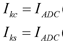
Eqns. (58): QKC = QADC (n)∞ ωηΙί ηΤ), and

Eqn. (59): PI = BPF {I kc + Q
BPF {[—cos( a>mlnT ) +—cos( a>m2nT )] cos( a>knT ) +
[■^■sm( a>mlnT - φ + comlAT) - -j sm( a>m2nT + φ + m2AT)]s {a>knT)
A A
= BPF {— cos( comlnT) cos( coknT) + ~SU1( ω min^ ) s^ ( 0} k n^) ~
A B
— sin(^ - >mlAT) cos( comlnT) sin( coknT) +— cos( cos( knT) -

[00120] Filtering with a bandpass filter centered at cok and ignoring the mismatch component of A results in
A B
Eqn. (60): P\ =—cos[( ml - k)nTs} +—^(φ + m2AT)sm[( m2 - k)nTs]
Similarly,
Eqn. (61): P2 = BPF {IB + Q , similarly leading to
A B
P2 = -— sin(<z> - comlAT)cos[(coml -<¾)«¾]- ycos[(<»ra2
V 1* 2 A2 B2
Eqn. (62): = -— η(φ - comlAT) -—ύη(φ + com2AT .
TV 16 16
[00121] Approximating sin(x) = x for small values of x results in P\*P2 ∑A2 +∑B7
Eqn. (63): -<p\r ■} + ΔΓ){- ■};
N 16 16
5
Eqn. (64): 3 = [yCOs{(«ml - ο^ηΓί} +—sin(p + <B1Il2A7,)sin{( - a>knTs}]
A
— cos3{(«ml +
-sin(^ + iyra2Ar)cos2{(iyral - k )tiTs) sin{( <yra2 - 6^ )«¾}
16
3AB2 2 2
■sin (^ε + a>m2 T) cos{( e>ml - a>k )nTs} sin {(itf„2 - cok )nTs}
32
53 .
sin3(^ + iym2Ar)sin3{(¾2 -<¾)/i7¾};
64
3Y A3 3Y A2B Eqn. (65): ∑Pl3P2 = -ήη{φ -ωη1Μ)^— - η{φ + ωη2Μ) ^
Eqn. (66):
_ , 3V / 3T A2B2 3ω 2 Τ Α2Β2 3ω . Y A4
α Ρ Ρ2 = -φ{-^ + } - AT{- m2 L ml j
256 64 64 256
[00122] Squaring and accumulating terms in Equations 58 and 59 results


128
Using equations 67, 68 and 69, equations 63 and 64 can be solved for φ and ΔΤ.
[00123] An additional advantage in this scheme of correcting the mismatch is that the correction at a frequency can be gated by the power spectrum at the frequency. If the power at a frequency band is observed to be less than a predetermined threshold, we can choose not to adapt the filter coefficients for that band.
[00124] This scheme need not be limited to background estimation and correction, but can be used as one time calibration where the mismatches of a device are determined once and the coefficients are trimmed to remove the mismatch. The algorithm can be adapted as a partial background and partial one-time trim. For example, the group delay mismatch can be made a one-time calibration and the phase mismatch can be used repeatedly in a background correction algorithm.
[00125] In some cases it may be most beneficial to split the I and Q signals into multiple bands using a phase splitter, and then, separate out the phase mismatch and the filter delay mismatch in each band. In other cases it may not be necessary to perform the distinguishing of filter delay mismatch and mixer input signal phase mismatch.
[00126] Those skilled in the art will appreciate that modifications may be made to the described embodiments, and also that many other embodiments are possible, within the scope of the claimed invention.
Claims
1. A system for correcting gain imbalance and phase imbalance between first and second signals which are 90° out of phase, the system comprising:
circuitry for estimating the phase mismatch and gain mismatch between the first signal and the second signal signals at a plurality of frequency bands; and
circuitry for performing an inverse fast Fourier transform (IFFT) on each of a number of arrays of the phase mismatch estimates and the gain mismatch estimates to generate correction filter coefficients for a N tap correction filter;
wherein the N tap correction filter filters an uncorrected value of the second signal to generate a corrected value of the second signal.
2. The system of claim 1, wherein the estimating circuitry performs a function of distinguishing filter delay mismatches and mixer phase mismatches of the first signal and the second signal signals at the plurality of frequency bands.
3. The system of claim 1, including circuitry for splitting each of the first and second signals into a predetermined number of frequency bands to provide a plurality of in-phase and quadrature-phase signals in the frequency bands, respectively, and circuitry for successively producing a phase mismatch estimate and a gain mismatch estimate
corresponding to the successive frequency bands, respectively, on the basis of samples of the in-phase and quadrature-phase signals in the frequency bands.
4. The system of claim 3, wherein the splitting circuitry includes a bank of filters for splitting each of the first and second signals into the predetermined number of frequency bands, and wherein the estimating circuitry operates to successively produce a plurality of pairs of mismatch estimates corresponding to the plurality of successive frequency bands, respectively, on the basis of samples of in-phase and quadrature-phase signal values generated by the bank of filters, each pair including a phase mismatch estimate and a gain mismatch estimate, and wherein the inverse fast Fourier transform performing circuitry
performs an inverse fast Fourier transform (IFFT) on each of a number of arrays of the phase mismatch estimates and gain mismatch estimates to generate filter coefficients for an N tap filter for filtering an uncorrected value of the second signal to generate a corrected value of the second signal.
5. The system of claim 4, including a DC phase correction circuit including a mixer for mixing the first signal with a DC mismatch adjustment value and an adder for adding an output of the mixer to the second signal to generate the uncorrected value of the second signal such that the N tap filter essentially eliminates the gain imbalance and the phase imbalance between the first and second signals across all of the frequency bands.
6. The system of claim 4, wherein the phase mismatch estimates are determined in accordance with the equation
I, Q, + I. Q.
sin( φ) =
Q ts Q kc
where φ is a phase mismatch estimate, Ike is a cosine-related in-phase signal in a
predetermined frequency band produced by the bank of filters, Qkc is a cosine-related quadrature signal in the predetermined frequency band produced by the bank of filters, Iks is a sine-related in-phase signal in a predetermined frequency band produced by the bank of filters, and Qks is a sine-related quadrature signal in the predetermined frequency band produced by the bank of filters.
7. The system of claim 4, wherein the gain mismatch estimates are determined in accordance with equation

where Δ is a gain mismatch estimate, Ike is a cosine -related in-phase signal in a
predetermined frequency band produced by the bank of filters, Qkc is a cosine-related quadrature signal in the predetermined frequency band produced by the bank of filters, Iks is a sine-related in-phase signal in the predetermined frequency band produced by the bank of
filters, and Qks is a sine-related quadrature signal in the predetermined frequency band produced by the bank of filters.
8. The system of claim 4, wherein the N tap filter includes a finite impulse response filter (FIR).
9. The system of claim 4, wherein the number of arrays of the phase mismatch estimates and gain mismatch estimates represent a mismatch estimate frequency response of an IQ system through which the first and second signals pass.
10. The system of claim 4, wherein the bank of filters includes a plurality of mixing and filtering circuits for mixing the first signal with a plurality of first reference signals and for mixing the second signal with a plurality of second reference signals which are shifted 90° relative to a corresponding first reference signal, respectively, and also includes low pass filtering outputs of the various mixed signals to provide the samples of the in-phase and quadrature-phase signal values generated by the bank of filters.
11. The system of claim 5, wherein the number of arrays are included in a primary feedback loop also including the bank of filters, the estimating circuitry, and the fast Fourier transform performing circuitry, and wherein the DC mismatch adjustment value is provided as an input to a secondary feedback loop including the mixer for mixing the first signal with the DC mismatch adjustment value and the adder to generate the uncorrected value of the second signal.
12. The system of claim 11, wherein the primary and secondary loops are independent.
13. The system of claim 1, wherein the first signal is produced by a first analog to digital converter in response to an in-phase analog signal, and the second signal is produced by a second analog to digital converter in response to quadrature-phase analog signal.
14. The system of claim 1, wherein the first signal is an in-phase signal and the second signal is a quadrature -phase signal.
15. A method for correcting gain imbalance and phase imbalance between first and second signals which are 90° out of phase, the method comprising:
estimating the phase mismatch and gain mismatch between the first signal and the second signal signals in a plurality of frequency bands;
performing an inverse fast Fourier transform (IFFT) on each of a number of arrays of the phase mismatch estimates and a gain mismatch estimates to generate filter coefficients for an N tap correction filter; and
filtering an uncorrected value of the second signal by means of the an N tap correction filter to generate a corrected value of the second signal.
16. The method of claim 15, including distinguishing filter delay mismatch components and mixer phase input mismatch components of the first signal and the second signal signals in the multiple bands of frequencies and using the filter delay mismatch components and mixer phase input mismatch components separately to correct them, respectively.
17. The method of claim 15, including providing each of the first and signals in a predetermined number of frequency bands to provide a plurality of in-phase and
quadrature-phase signals in the frequency bands, respectively, and successively producing a phase mismatch estimate and a gain mismatch estimate corresponding to the successive frequency bands, respectively, on the basis of samples of the in-phase and quadrature-phase signals in the frequency bands.
18. The method of claim 17, including generating a DC mismatch adjustment value on the basis of a phase mismatch estimate at zero frequency, mixing the first signal with the DC mismatch adjustment value and an adder, and adding an output of a mixer to the second signal to generate a value of the second signal such that the N tap filter essentially eliminates the gain imbalance and the phase imbalance between the first and signals at DC
and across all of the frequency bands.
19. The method of claim 17, including determining the phase mismatch estimates in accordance with the e uation

and determining the gain mismatch estimates in accordance with equation
 where φ is a phase mismatch estimate, Δ is a gain mismatch estimate, Ike is a cosine-related in-phase signal in a predetermined frequency band, Qkc is a cosine-related quadrature signal in the predetermined frequency band, Iks is a sine-related in-phase signal in the
predetermined frequency band, and Qks is a sine -related quadrature signal in the
predetermined frequency band.
20. The method of claim 17, wherein the estimating includes computing the gain mismatch and the phase mismatch using discrete Fourier transforms in accordance with the equations
N-l 2mk
Xi_ real {k) =∑ 7(«) cos( 0
N
Xi_ imag (k) =∑ 7(n) sin( _________.)
Xq _ real (k) = )

∑N I ink
Q(n) sm( )
GainMismatch =
Xi_ real + Xi_ imag - Xq _ real + Xq_ imag )
E(Xi_ real 2 + Xi_ imag 2 ) and PhaseMismatch = E phase - Qphase - 90 deg)
_! Xi imag _x Xq imag
= E(tan (— = — ) - E(tan (—— — )
Xi _ real Xq _ real
where E represents an averaging operation, k varies from 0 to N, N represents the number of points in an IFFT, and n represents the sample number.
21. A system for correcting gain imbalance and phase imbalance between first and second signals which are 90° out of phase, comprising:
means for estimating the phase mismatch and gain mismatch between the first signal and the second signal signals in a plurality of frequency bands; and
means for performing an inverse fast Fourier transform (IFFT) on each of a number of arrays of the phase mismatch estimates and a gain mismatch estimates to generate filter coefficients for an N tap correction filter;
wherein the N tap correction filter filters an uncorrected value of the second signal to generate a corrected value of the second signal.
22. The system of claim 21, including means for providing each of the first and signals in a predetermined number frequency bands to provide a plurality of in-phase and quadrature-phase signals in the frequency bands, respectively, and means for successively producing a phase mismatch estimate and a gain mismatch estimate corresponding to the successive frequency bands, respectively, on the basis of samples of the in-phase and quadrature-phase signals in the frequency bands.
23. The system of claim 21, including means for distinguishing filter delay mismatch components and mixer phase mismatch components of the first signal and the second signal signals in the multiple bands of frequencies.
Priority Applications (1)
| Application Number | Priority Date | Filing Date | Title |
|---|---|---|---|
| CN201380035183.4A CN104412553B (en) | 2012-07-27 | 2013-07-16 | Multi-tap IQ imbalance estimation and correction circuit and method |
Applications Claiming Priority (2)
| Application Number | Priority Date | Filing Date | Title |
|---|---|---|---|
| US13/560,020 | 2012-07-27 | ||
| US13/560,020 US8976914B2 (en) | 2012-07-27 | 2012-07-27 | Multi-tap IQ imbalance estimation and correction circuit and method |
Publications (1)
| Publication Number | Publication Date |
|---|---|
| WO2014018303A1 true WO2014018303A1 (en) | 2014-01-30 |
Family
ID=49994898
Family Applications (1)
| Application Number | Title | Priority Date | Filing Date |
|---|---|---|---|
| PCT/US2013/050603 Ceased WO2014018303A1 (en) | 2012-07-27 | 2013-07-16 | Multi-tap iq imbalance estimation and correction circuit and method |
Country Status (3)
| Country | Link |
|---|---|
| US (1) | US8976914B2 (en) |
| CN (1) | CN104412553B (en) |
| WO (1) | WO2014018303A1 (en) |
Cited By (2)
| Publication number | Priority date | Publication date | Assignee | Title |
|---|---|---|---|---|
| US20170019240A1 (en) * | 2015-07-16 | 2017-01-19 | LGS Innovations LLC | Tone based in-phase and quadrature-phase (iq) compensation |
| US9906384B1 (en) | 2016-09-26 | 2018-02-27 | Nxp B.V. | Multiple-tap compensation and calibration |
Families Citing this family (11)
| Publication number | Priority date | Publication date | Assignee | Title |
|---|---|---|---|---|
| US9088471B1 (en) * | 2014-02-19 | 2015-07-21 | Qualcomm Incorporated | Quadrature combining and adjusting |
| KR101674747B1 (en) * | 2014-11-18 | 2016-11-09 | 재단법인대구경북과학기술원 | Apparatus and method for processing radar signal with in-phase/quadrature-phase imbalance |
| EP3068044A1 (en) * | 2015-03-11 | 2016-09-14 | Nxp B.V. | Module for a radio receiver |
| CN105471779B (en) | 2015-12-08 | 2018-08-31 | 扬智科技股份有限公司 | correction method and correction circuit |
| EP3267646B1 (en) | 2016-07-06 | 2021-06-02 | Nxp B.V. | Iq mismatch correction module |
| CN107819720B (en) * | 2016-09-12 | 2020-04-10 | 深圳市中兴微电子技术有限公司 | IQ imbalance compensation method and device, time domain compensator and communication equipment |
| US10816655B2 (en) * | 2016-12-07 | 2020-10-27 | Texas Instruments Incorporated | In-phase (I) and quadrature (Q) imbalance estimation in a radar system |
| GB201801412D0 (en) * | 2018-01-29 | 2018-03-14 | National Univ Of Ireland | Characterising radio frequency signal processing paths |
| US10715376B2 (en) * | 2018-11-02 | 2020-07-14 | Texas Instruments Incorporated | Enhanced IQ mismatch correction function generator |
| EP4020002A1 (en) * | 2020-12-22 | 2022-06-29 | NXP USA, Inc. | Method and device for determining the phase error of a phase rotator |
| CN118041464B (en) * | 2022-11-11 | 2025-12-19 | 中兴通讯股份有限公司 | Radio frequency signal correction device, method and radio frequency transmitting device |
Citations (5)
| Publication number | Priority date | Publication date | Assignee | Title |
|---|---|---|---|---|
| US20040203472A1 (en) * | 2002-09-05 | 2004-10-14 | G-Plus, Inc. | Compensation of I-Q imbalance in digital transceivers |
| US20050069050A1 (en) * | 2003-09-30 | 2005-03-31 | Lei Ding | Frequency based modulator compensation |
| US20080063113A1 (en) * | 2006-09-07 | 2008-03-13 | Via Technologies, Inc. | Compensation for gain imbalance, phase imbalance and DC offsets in a transmitter |
| US20100215125A1 (en) * | 2009-02-25 | 2010-08-26 | Harris Corporation | Communications device with in-phase/quadrature (i/q) dc offset, gain and phase imbalance compensation and related method |
| US20110260898A1 (en) * | 2007-04-30 | 2011-10-27 | Velazquez Scott R | Mismatch compensators and methods for mismatch compensation |
Family Cites Families (11)
| Publication number | Priority date | Publication date | Assignee | Title |
|---|---|---|---|---|
| US5872538A (en) | 1998-02-26 | 1999-02-16 | Lockheed Martin Corporation | Frequency domain correction of I/Q imbalance |
| US6340883B1 (en) | 1998-09-03 | 2002-01-22 | Sony/Tektronik Corporation | Wide band IQ splitting apparatus and calibration method therefor with balanced amplitude and phase between I and Q |
| US6330290B1 (en) | 1998-09-25 | 2001-12-11 | Lucent Technologies, Inc. | Digital I/Q imbalance compensation |
| US7088765B1 (en) * | 2000-03-15 | 2006-08-08 | Ndsu Research Foundation | Vector calibration system |
| US7177372B2 (en) | 2000-12-21 | 2007-02-13 | Jian Gu | Method and apparatus to remove effects of I-Q imbalances of quadrature modulators and demodulators in a multi-carrier system |
| US6785529B2 (en) | 2002-01-24 | 2004-08-31 | Qualcomm Incorporated | System and method for I-Q mismatch compensation in a low IF or zero IF receiver |
| WO2005029798A1 (en) * | 2003-09-15 | 2005-03-31 | Intel Corporation | Adaptive iq imbalance correction for multicarrier wireless communication systems |
| US8208530B2 (en) * | 2005-03-14 | 2012-06-26 | Broadcom Corporation | Apparatus and method for correcting IQ imbalance |
| WO2008026178A2 (en) * | 2006-08-31 | 2008-03-06 | Nxp B.V. | Frequency dependent i/q imbalance estimation |
| CN101815056B (en) * | 2010-03-05 | 2012-09-05 | 华为技术有限公司 | IQ unbalanced calibration method and equipment of baseband signals in wireless communication receiving machine |
| US8331506B2 (en) * | 2010-03-12 | 2012-12-11 | Telefonaktiebolaget L M Ericsson (Publ) | Frequency-dependent IQ imbalance estimation |
-
2012
- 2012-07-27 US US13/560,020 patent/US8976914B2/en active Active
-
2013
- 2013-07-16 WO PCT/US2013/050603 patent/WO2014018303A1/en not_active Ceased
- 2013-07-16 CN CN201380035183.4A patent/CN104412553B/en active Active
Patent Citations (5)
| Publication number | Priority date | Publication date | Assignee | Title |
|---|---|---|---|---|
| US20040203472A1 (en) * | 2002-09-05 | 2004-10-14 | G-Plus, Inc. | Compensation of I-Q imbalance in digital transceivers |
| US20050069050A1 (en) * | 2003-09-30 | 2005-03-31 | Lei Ding | Frequency based modulator compensation |
| US20080063113A1 (en) * | 2006-09-07 | 2008-03-13 | Via Technologies, Inc. | Compensation for gain imbalance, phase imbalance and DC offsets in a transmitter |
| US20110260898A1 (en) * | 2007-04-30 | 2011-10-27 | Velazquez Scott R | Mismatch compensators and methods for mismatch compensation |
| US20100215125A1 (en) * | 2009-02-25 | 2010-08-26 | Harris Corporation | Communications device with in-phase/quadrature (i/q) dc offset, gain and phase imbalance compensation and related method |
Cited By (2)
| Publication number | Priority date | Publication date | Assignee | Title |
|---|---|---|---|---|
| US20170019240A1 (en) * | 2015-07-16 | 2017-01-19 | LGS Innovations LLC | Tone based in-phase and quadrature-phase (iq) compensation |
| US9906384B1 (en) | 2016-09-26 | 2018-02-27 | Nxp B.V. | Multiple-tap compensation and calibration |
Also Published As
| Publication number | Publication date |
|---|---|
| CN104412553B (en) | 2018-10-16 |
| US20140029700A1 (en) | 2014-01-30 |
| US8976914B2 (en) | 2015-03-10 |
| CN104412553A (en) | 2015-03-11 |
Similar Documents
| Publication | Publication Date | Title |
|---|---|---|
| WO2014018303A1 (en) | Multi-tap iq imbalance estimation and correction circuit and method | |
| CN100477489C (en) | Quadrature demodulator using FFT processor | |
| US9780891B2 (en) | Method and device for calibrating IQ imbalance and DC offset of RF tranceiver | |
| EP2313980B1 (en) | Methods and apparatus for suppressing strong-signal interference in low-if receivers | |
| EP1339197A1 (en) | I/Q Mismatch compensation in an OFDM receiver in presence of frequency offset | |
| KR101884492B1 (en) | Controllable frequency offset for inphase and quadrature (iq) imbalance estimation | |
| US20050107059A1 (en) | Compensation of mismatch between quadrature paths | |
| CN102257734A (en) | Interference cancellation in an OFDM receiver | |
| KR100845416B1 (en) | Frequency correction by symmetrical phase adjustment in each ODF symbol | |
| US9106326B2 (en) | Method for determining the imperfections of a transmit pathway and of a receive pathway of an apparatus, and associated radio apparatus | |
| WO2018009827A1 (en) | Digital compensation of iq coupling in communication receivers | |
| US7310388B2 (en) | Direct conversion receiver and receiving method | |
| KR100809206B1 (en) | Time Domain IV Mismatch Detection of Orthogonal Frequency Division Multiple Receivers | |
| JP4925462B2 (en) | Receiving machine | |
| De Witt | Modelling, estimation and compensation of imbalances in quadrature transceivers | |
| US7778359B2 (en) | Method and device for clock synchronisation with a vestigial-sideband-modulated transmitted signal | |
| US20020009162A1 (en) | Method and apparatus for correcting a signal | |
| CN106330796A (en) | Mismatch compensation device and method and mismatch detection device | |
| EP1515429B1 (en) | Direct conversion receiver and receiving method | |
| KR20170103600A (en) | Method and device for calibrating iq imbalance and dc offset of rf tranceiver | |
| EP2797225B1 (en) | Method of and apparatus for demodulating an amplitude modulated signal | |
| JP2943803B1 (en) | Receiver | |
| Thesling | Digital Cross-Polar Interference Canceller |
Legal Events
| Date | Code | Title | Description |
|---|---|---|---|
| 121 | Ep: the epo has been informed by wipo that ep was designated in this application |
Ref document number: 13822641 Country of ref document: EP Kind code of ref document: A1 |
|
| NENP | Non-entry into the national phase |
Ref country code: DE |
|
| 122 | Ep: pct application non-entry in european phase |
Ref document number: 13822641 Country of ref document: EP Kind code of ref document: A1 |