WO2013161645A1 - Matériau de conversion thermoélectrique et son procédé de fabrication - Google Patents
Matériau de conversion thermoélectrique et son procédé de fabrication Download PDFInfo
- Publication number
- WO2013161645A1 WO2013161645A1 PCT/JP2013/061416 JP2013061416W WO2013161645A1 WO 2013161645 A1 WO2013161645 A1 WO 2013161645A1 JP 2013061416 W JP2013061416 W JP 2013061416W WO 2013161645 A1 WO2013161645 A1 WO 2013161645A1
- Authority
- WO
- WIPO (PCT)
- Prior art keywords
- conversion material
- thermoelectric
- thermoelectric conversion
- resin substrate
- resin
- Prior art date
Links
Images


Classifications
-
- H—ELECTRICITY
- H10—SEMICONDUCTOR DEVICES; ELECTRIC SOLID-STATE DEVICES NOT OTHERWISE PROVIDED FOR
- H10N—ELECTRIC SOLID-STATE DEVICES NOT OTHERWISE PROVIDED FOR
- H10N10/00—Thermoelectric devices comprising a junction of dissimilar materials, i.e. devices exhibiting Seebeck or Peltier effects
- H10N10/80—Constructional details
- H10N10/85—Thermoelectric active materials
- H10N10/851—Thermoelectric active materials comprising inorganic compositions
- H10N10/852—Thermoelectric active materials comprising inorganic compositions comprising tellurium, selenium or sulfur
-
- H—ELECTRICITY
- H10—SEMICONDUCTOR DEVICES; ELECTRIC SOLID-STATE DEVICES NOT OTHERWISE PROVIDED FOR
- H10N—ELECTRIC SOLID-STATE DEVICES NOT OTHERWISE PROVIDED FOR
- H10N10/00—Thermoelectric devices comprising a junction of dissimilar materials, i.e. devices exhibiting Seebeck or Peltier effects
- H10N10/80—Constructional details
- H10N10/81—Structural details of the junction
- H10N10/817—Structural details of the junction the junction being non-separable, e.g. being cemented, sintered or soldered
-
- H—ELECTRICITY
- H10—SEMICONDUCTOR DEVICES; ELECTRIC SOLID-STATE DEVICES NOT OTHERWISE PROVIDED FOR
- H10N—ELECTRIC SOLID-STATE DEVICES NOT OTHERWISE PROVIDED FOR
- H10N10/00—Thermoelectric devices comprising a junction of dissimilar materials, i.e. devices exhibiting Seebeck or Peltier effects
- H10N10/80—Constructional details
- H10N10/85—Thermoelectric active materials
-
- B—PERFORMING OPERATIONS; TRANSPORTING
- B29—WORKING OF PLASTICS; WORKING OF SUBSTANCES IN A PLASTIC STATE IN GENERAL
- B29C—SHAPING OR JOINING OF PLASTICS; SHAPING OF MATERIAL IN A PLASTIC STATE, NOT OTHERWISE PROVIDED FOR; AFTER-TREATMENT OF THE SHAPED PRODUCTS, e.g. REPAIRING
- B29C39/00—Shaping by casting, i.e. introducing the moulding material into a mould or between confining surfaces without significant moulding pressure; Apparatus therefor
- B29C39/02—Shaping by casting, i.e. introducing the moulding material into a mould or between confining surfaces without significant moulding pressure; Apparatus therefor for making articles of definite length, i.e. discrete articles
-
- H—ELECTRICITY
- H10—SEMICONDUCTOR DEVICES; ELECTRIC SOLID-STATE DEVICES NOT OTHERWISE PROVIDED FOR
- H10N—ELECTRIC SOLID-STATE DEVICES NOT OTHERWISE PROVIDED FOR
- H10N10/00—Thermoelectric devices comprising a junction of dissimilar materials, i.e. devices exhibiting Seebeck or Peltier effects
- H10N10/01—Manufacture or treatment
-
- H—ELECTRICITY
- H10—SEMICONDUCTOR DEVICES; ELECTRIC SOLID-STATE DEVICES NOT OTHERWISE PROVIDED FOR
- H10N—ELECTRIC SOLID-STATE DEVICES NOT OTHERWISE PROVIDED FOR
- H10N10/00—Thermoelectric devices comprising a junction of dissimilar materials, i.e. devices exhibiting Seebeck or Peltier effects
- H10N10/10—Thermoelectric devices comprising a junction of dissimilar materials, i.e. devices exhibiting Seebeck or Peltier effects operating with only the Peltier or Seebeck effects
- H10N10/17—Thermoelectric devices comprising a junction of dissimilar materials, i.e. devices exhibiting Seebeck or Peltier effects operating with only the Peltier or Seebeck effects characterised by the structure or configuration of the cell or thermocouple forming the device
-
- Y—GENERAL TAGGING OF NEW TECHNOLOGICAL DEVELOPMENTS; GENERAL TAGGING OF CROSS-SECTIONAL TECHNOLOGIES SPANNING OVER SEVERAL SECTIONS OF THE IPC; TECHNICAL SUBJECTS COVERED BY FORMER USPC CROSS-REFERENCE ART COLLECTIONS [XRACs] AND DIGESTS
- Y02—TECHNOLOGIES OR APPLICATIONS FOR MITIGATION OR ADAPTATION AGAINST CLIMATE CHANGE
- Y02E—REDUCTION OF GREENHOUSE GAS [GHG] EMISSIONS, RELATED TO ENERGY GENERATION, TRANSMISSION OR DISTRIBUTION
- Y02E10/00—Energy generation through renewable energy sources
- Y02E10/50—Photovoltaic [PV] energy
Definitions
- the present invention relates to a thermoelectric conversion material that performs mutual energy conversion between heat and electricity, and more particularly, to a thermoelectric conversion material having a high thermoelectric performance index using a resin substrate and a method for manufacturing the same.
- thermoelectric power generation technology that has a simple system and can be reduced in size has attracted attention as a recovery power generation technology for unused waste heat energy generated from fossil fuel resources used in buildings, factories, and the like.
- thermoelectric power generation generally has poor power generation efficiency, and various companies and research institutions are actively researching and developing power generation efficiency.
- it is essential to improve the efficiency of thermoelectric conversion materials. To achieve these, development of materials with high electrical conductivity similar to metal and low thermal conductivity comparable to glass is desired. It is rare.
- S is a Seebeck coefficient
- ⁇ electrical conductivity (reciprocal of resistivity)
- ⁇ thermal conductivity.
- thermoelectric figure of merit has not been improved significantly.
- Patent Document 1 introduces a number of very fine vacancies dispersed in the semiconductor material at intervals equal to or less than the mean free path of electrons and phonons to make it porous. Thermoelectric conversion materials with reduced thermal conductivity and increased Seebeck coefficient have been proposed.
- Patent Document 1 although the thermal conductivity is reduced, the electrical conductivity is also reduced (the resistivity is greatly increased), and the dimensionless thermoelectric figure of merit ZT (T: calculated as an absolute temperature of 300K) is obtained. Increased from 0.017 to 0.156 due to porosity, but the absolute value was far from ZT ⁇ 1, which is an index value for practical use.
- Patent Document 2 discloses that the thermoelectric conversion material is improved by nanoimprinting to produce a thin thermoelectric conversion material. However, the decrease in thermal conductivity is small and sufficient performance is achieved. Was not obtained.
- an object of the present invention is to provide a thermoelectric conversion material having a reduced thermal conductivity and an improved thermoelectric performance index, and a method for producing the same.
- the present inventors have made a curable resin as the resin substrate in a thermoelectric conversion material in which a thermoelectric semiconductor layer made of a thermoelectric semiconductor material is formed on a resin substrate having a recess.
- the inventors have found that the thermoelectric figure of merit is improved by using a composition, for example, a cured resin layer made of an energy beam curable resin composition, and completed the present invention. That is, the present invention provides the following (1) to (15).
- the resin substrate is formed by curing a resin layer made of a curable resin composition.
- Thermoelectric conversion material (2) The thermoelectric conversion material according to (1), wherein the curable resin composition is an energy ray curable resin composition. (3) The said resin substrate is obtained by making it harden
- thermoelectric conversion material The thermoelectric conversion material according to any one of (1) to (5), wherein the resin substrate has a thickness of 1 to 100 ⁇ m. (7) The thermoelectric conversion material according to any one of (1) to (6), wherein the resin substrate has a large number of independent recesses. (8) The thermoelectric conversion material according to any one of (1) to (7), wherein the shape of the recess is a columnar shape or a groove shape.
- thermoelectric conversion material according to (8), wherein the depth of the recess is 5 to 10,000 nm, the diameter or groove width of the recess is 10 to 5000 nm, and the distance between the centers of adjacent recesses is 15 to 5500 nm.
- the thermoelectric semiconductor layer is present on the upper surface of the resin substrate, and the inner bottom portion of the recess and the upper surface maintain insulation.
- the thermoelectric conversion material in any one.
- (11) The thermoelectric conversion material according to any one of (1) to (10) above, wherein the thermoelectric semiconductor layer has a thickness of 10 to 5000 nm.
- thermoelectric conversion material according to any one of (1) to (11), wherein the thermoelectric semiconductor material is a bismuth-tellurium-based thermoelectric semiconductor material or a bismuth selenide-based thermoelectric semiconductor material.
- thermoelectric conversion material is a bismuth-tellurium-based thermoelectric semiconductor material or a bismuth selenide-based thermoelectric semiconductor material.
- thermoelectric conversion material in which a thermoelectric semiconductor layer is formed on a resin substrate having recesses, wherein the protrusions are transferred from an original plate having a protrusion structure to a resin layer made of a curable resin composition. Production of a thermoelectric conversion material comprising: a resin substrate manufacturing step formed by transferring and curing a partial structure; and a film forming step of forming a thermoelectric semiconductor layer by forming a thermoelectric semiconductor material on the resin substrate Method.
- the resin substrate manufacturing step includes a resin layer forming step of forming a resin layer with the curable resin composition, the resin layer and the original plate are pressed against each other, and the convex portion of the original plate is applied to the resin layer.
- the method for producing a thermoelectric conversion material according to the above (13), comprising a transfer step of transferring the structure and a step of forming a recess by curing the resin layer and then releasing from the original plate to form a recess.
- thermoelectric conversion material having a low thermal conductivity and an improved thermoelectric figure of merit can be obtained, and high conversion efficiency can be realized.
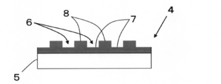
- thermoelectric-semiconductor layer which consists of thermoelectric-semiconductor materials in the resin substrate used for this invention is shown, (a) has the thermoelectric-semiconductor layer in the upper surface of a resin substrate, and the inner bottom part of a recessed part. In this case, (b) is a cross-sectional view when the thermoelectric semiconductor layer exists only on the upper surface of the resin substrate.
- thermoelectric conversion material obtained in Example 1 and Example 2 of this invention is shown, (a) is a SEM photograph (measurement magnification 10,000 times) of the thermoelectric conversion material of Example 1, (b) is implementation.
- thermoelectric conversion material of Example 4 is a SEM photograph (measurement magnification of 10,000 times) of the thermoelectric conversion material of Example 2.
- the plane of the thermoelectric conversion material obtained in Example 3 of this invention is shown, (a) is the SEM photograph (measurement magnification of 10000 times) of the thermoelectric conversion material of the part which consists of a cylindrical pattern which is one of pattern mixes.
- (B) is the SEM photograph (measurement magnification of 10000 times) of the thermoelectric conversion material of the part which consists of a groove-like pattern of a pattern mix.
- thermoelectric conversion material of the present invention is a thermoelectric conversion material in which a thermoelectric semiconductor layer made of a thermoelectric semiconductor material is formed on a resin substrate having a recess, and the resin substrate hardens a resin layer made of a curable resin composition. It is characterized by.
- FIG. 1 is a cross-sectional view showing an example of an original plate (nanoimprint mold) used in the production method of the present invention described later.
- a predetermined convex structure 3 is formed on a substrate 2.
- the convex structure 3 is usually formed in a shape that takes into account the nanostructure obtained after transfer, although it depends on the application.
- quartz transparent on the long wavelength side from 193 nm
- the nanoimprint mold used as the original plate 1 can be produced by lithography or the like, but the production method is not particularly limited, and a known method can be used.
- a positive resist is applied to the entire surface of the base material 2 as a molding material, electron beam drawing or ultraviolet exposure is performed on the positive resist to form a predetermined resist pattern, and the obtained resist pattern is etched into an etching mask.
- the substrate 2 is wet or dry etched, finally the resist residue is removed, and the convex structure 3 is formed to manufacture the nanoimprint mold.
- a commercial item can also be used for the nanoimprint mold. Commercial products are commercially available from, for example, NTT-AT.
- the convex structure 3 of the original 1 there are various shapes of the convex structure 3 of the original 1 and it is not particularly limited. For example, the following shapes are mentioned, which are used as appropriate according to the application.
- A) Dot shape the shape of the convex portion is a dot shape such as a circle, an ellipse, or a polygon.
- B) Line shape the shape of the convex portion is a line shape such as a straight line or a curved line).
- C Pattern mix shape (mixed dot shape and line shape).
- the pattern of the original 1 used by this invention should just be independent in convex parts, and may be bent not only a straight line. In addition, the arrangement may or may not be continuous or regular.
- FIG. 2 is a cross-sectional view showing an example of a resin substrate used in the present invention.
- the resin substrate 4 having the recess 6 is formed on the support 5.
- the resin substrate 4 is obtained by, for example, transferring the original plate 1 having the convex structure 3 to a resin layer made of a curable resin composition, curing, and releasing the mold. It can be obtained by being transferred as an inverted pattern of the convex structure 3 of the original 1.
- the curable resin composition only needs to have insulating properties and be curable, and examples thereof include an energy ray curable resin and a thermosetting resin as a main component. Among them, from the point that heat resistance is high, deformation is not caused by heat, and low thermal conductivity can be maintained, the curable resin composition is an energy ray curable resin composition mainly composed of an energy ray curable resin. Preferably there is.
- the thermal conductivity of the resin substrate 4 can be reduced, and the thermoelectric performance index of the thermoelectric conversion material can be improved.
- the energy beam curable resin composition is not particularly limited.
- a resin containing a (meth) acrylic acid ester copolymer having an energy beam curable group in the side chain or 2) an energy beam.
- examples include those containing a polymer having no curability and energy ray curable monomers and / or oligomers, and 3) those containing energy ray curable monomers and / or oligomers as main components.
- thermoelectric conversion material By using a resin composition containing such a copolymer, a relatively thick resin layer can be formed, so that a resin substrate having excellent heat resistance can be obtained.
- the obtained resin substrate is used. Even when the thermoelectric conversion material is driven at a high temperature for a long time, it is difficult for the resin substrate to be thermally deformed, and it is possible to suppress a decrease in thermoelectric performance.
- the energy ray curable resin composition may be referred to as 1) a (meth) acrylic acid ester copolymer having an energy ray curable group in the side chain (hereinafter referred to as “energy ray curable copolymer”). ) Will be described.
- (meth) acrylic acid in the present specification means both acrylic acid and methacrylic acid.
- the (meth) acrylic acid ester copolymer having an energy ray-curable group in the side chain As the (meth) acrylic acid ester copolymer having an energy ray-curable group in the side chain, the (meth) acrylic copolymer (m1) having a functional group-containing monomer unit and the functional group are reacted. It is obtained by reacting with an unsaturated group-containing compound (m2) having a substituent capable of forming a covalent bond.
- a resin composition containing such a copolymer a resin substrate having adhesiveness can be formed.For example, without using an adhesive layer, the resin substrate is directly connected to various devices such as a photoelectric conversion device, Can be attached to walls or buildings.
- the (meth) acrylic copolymer (m1) is composed of a structural unit derived from a functional group-containing monomer and a structural unit derived from a (meth) acrylic acid ester monomer or a derivative thereof.
- the functional group-containing monomer of the (meth) acrylic copolymer (m1) includes, for example, a polymerizable double bond and a functional group such as a hydroxyl group, a carboxyl group, an amino group, a substituted amino group, and an epoxy group.
- a monomer having in the molecule, a hydroxyl group-containing unsaturated compound and a carboxyl group-containing unsaturated compound are preferably used.
- the hydroxyl group-containing unsaturated compound includes hydroxyl group-containing (meth) acrylates such as 2-hydroxyethyl acrylate, 2-hydroxyethyl methacrylate, 2-hydroxypropyl acrylate, 2-hydroxybutyl acrylate, 2-hydroxybutyl methacrylate and the like.
- hydroxyl group-containing (meth) acrylates such as 2-hydroxyethyl acrylate, 2-hydroxyethyl methacrylate, 2-hydroxypropyl acrylate, 2-hydroxybutyl acrylate, 2-hydroxybutyl methacrylate and the like.
- carboxyl group-containing unsaturated compound include ethylenically unsaturated carboxylic acids such as acrylic acid, methacrylic acid, and itaconic acid. These may be used alone or in combination of two or more.
- the (meth) acrylic acid ester monomer constituting the (meth) acrylic copolymer (m1) includes benzylalkyl (meth) acrylate, cycloalkyl (meth) acrylate, and an alkyl group having 1 to 18 carbon atoms.
- Alkyl (meth) acrylates, etc. are used, and among these, alkyl (meth) acrylates having an alkyl group with 1 to 18 carbon atoms are preferably used.
- alkyl (meth) acrylate having an alkyl group having 1 to 18 carbon atoms include methyl (meth) acrylate, ethyl (meth) acrylate, propyl (meth) acrylate, n-butyl (meth) acrylate, Isobutyl (meth) acrylate, t-butyl (meth) acrylate, pentyl (meth) acrylate, hexyl (meth) acrylate, cyclohexyl (meth) acrylate, 2-ethylhexyl (meth) acrylate, isooctyl (meth) acrylate, decyl (meth) Examples include acrylate, dodecyl (meth) acrylate, myristyl (meth) acrylate, palmityl (meth) acrylate, stearyl (meth) acrylate, and among these, methyl (meth) acrylate and
- the (meth) acrylic copolymer (m1) can be obtained by copolymerizing a functional group-containing monomer as described above with a (meth) acrylic acid ester monomer or a derivative thereof by a known method. In addition to these monomers, other monomers may be copolymerized in a small amount (for example, 10% by mass or less, preferably 5% by mass or less).
- Other monomers include vinyl esters such as vinyl acetate and vinyl propionate; olefins such as ethylene, propylene and isobutylene; halogenated olefins such as vinyl chloride and vinylidene chloride; styrenes such as styrene and ⁇ -methylstyrene Monomers; Diene monomers such as butadiene, isoprene and chloroprene; Nitrile monomers such as acrylonitrile and methacrylonitrile; and acrylamides such as acrylamide, N-methylacrylamide and N, N-dimethylacrylamide. These can be used alone or in combination of two or more.
- the structural unit derived from the functional group-containing monomer is usually 3 to 100% by mass, preferably 5 to 40% by mass, particularly preferably 10 to 30% by mass.
- the structural unit derived from a (meth) acrylic acid ester monomer or derivative thereof is usually contained in a proportion of 0 to 97% by mass, preferably 60 to 95% by mass, particularly preferably 70 to 90% by mass. It becomes.
- the unsaturated group-containing compound (m2) needs to be appropriately selected according to the type of functional group of the functional group-containing monomer that the (meth) acrylic copolymer (m1) has. Therefore, for example, when the functional group of the functional group-containing monomer of the (meth) acrylic copolymer (m1) is a hydroxy group, an amino group, or a substituted amino group, the unsaturated group-containing compound (m2) has As the substituent, an isocyanate group or an epoxy group is preferable. When the functional group is a carboxyl group, the substituent is preferably an isocyanate group, an aziridinyl group, an epoxy group or an oxazoline group, and further has a functional group.
- the substituent is preferably an amino group, a carboxyl group or an aziridinyl group.
- One such substituent is included for each molecule of the unsaturated group-containing compound (m2).
- the unsaturated group-containing compound (m2) for example, methacryloyloxyethyl isocyanate, methacryloyl isocyanate, meta-isopropenyl- ⁇ , ⁇ -dimethylbenzyl isocyanate, allyl isocyanate; diisocyanate compound or poly Acrylyl monoisocyanate compound obtained by reaction of isocyanate compound with hydroxyethyl (meth) acrylate; obtained by reaction of diisocyanate compound or polyisocyanate compound, polyol compound and hydroxyethyl (meth) acrylate Acryloyl monoisocyanate compound; glycidyl (meth) acrylate; (meth) acrylic acid, 2- (1-aziridinyl
- the unsaturated group-containing compound (m2) is usually 20 to 100 equivalents, preferably 40 to 95 equivalents, particularly preferably 60 to 90 equivalents per 100 equivalents of the functional group-containing monomer of the (meth) acrylic copolymer (m1). Used in equivalent proportions.
- the reaction temperature, time, solvent, catalyst, etc. are appropriately selected according to the combination of the functional group and the substituent. Do it. From the above, the functional group present in the side chain in the (meth) acrylic copolymer (m1) reacts with the substituent in the unsaturated group-containing compound (m2), and the unsaturated group becomes (meth) acrylic.
- a (meth) acrylic acid ester copolymer introduced into the side chain in the system copolymer (m1) and having an energy ray-curable group in the side chain can be obtained.
- the weight average molecular weight (Mw) of the (meth) acrylic acid ester copolymer having an energy ray-curable group in the side chain is preferably 100,000 or more, more preferably 200,000 to 2,500,000. In view of heat resistance, it is particularly preferably 500,000 to 1,500,000.
- the weight average molecular weight in this specification was measured by gel permeation chromatography (GPC method) using the molecular weight of standard polystyrene.
- the curable resin composition preferably further contains a photopolymerization initiator in addition to the energy beam curable copolymer.
- a photopolymerization initiator By containing a photopolymerization initiator, the polymerization curing time and the amount of light irradiation can be reduced when photocuring after forming a resin layer made of an energy ray curable resin composition.
- the photopolymerization initiator is not particularly limited.
- 1-hydroxy-cyclohexyl-phenyl ketone 2-hydroxy-2-methyl-1-phenyl-propan-1-one, 2-methyl-1- (4 -Methylthiophenyl) -2-morpholinopropan-1-one, 2-benzyl-2-dimethylamino-1- (4-morpholinophenyl) -1-butanone, bis (2,4,6-trimethylbenzoyl)- Phenylphosphine oxide, 4-phenylbenzophenone, 4-phenoxybenzophenone, 4,4′-diphenylbenzophenone, 4,4′-diphenoxybenzophenone, benzophenone, acetophenone, benzoin, benzoin methyl ether, benzoin ethyl ether, benzoin isopropyl ether, Benzoin Sobutyl ether, benzoin benzoic acid, methyl benzoin benzoate, benzoin dimethyl ketal, 2,4-diethylthioxan
- 1-hydroxy-cyclohexyl-phenyl ketone is preferably used from the viewpoints of good reactivity with the energy rays to be used, optimum reaction rate, and progress of the reaction to the deep part of the resin layer. These may be used alone or in combination of two or more.
- the photopolymerization initiator is preferably used in an amount in the range of 0.1 to 10 parts by mass, particularly 0.5 to 5 parts by mass with respect to 100 parts by mass of the energy beam curable copolymer.
- the curable resin composition may appropriately contain other components in addition to the energy beam curable copolymer and the photopolymerization initiator.
- other components include a thermoplastic resin component, an energy ray-curable monomer and / or oligomer component described later, a crosslinking agent, and other additives.
- thermoplastic resin component examples include polyacrylic acid ester, polyester, polyurethane, polycarbonate, and polyolefin.
- a polyfunctional compound having reactivity with the functional group of the energy ray curable copolymer or the like can be used.
- examples of such polyfunctional compounds include isocyanate compounds, epoxy compounds, amine compounds, melamine compounds, aziridine compounds, hydrazine compounds, aldehyde compounds, oxazoline compounds, metal alkoxide compounds, metal chelate compounds, metal salts, ammonium salts. And reactive phenol resins.
- additives examples include ultraviolet absorbers, plasticizers, fillers, antioxidants, tackifiers, pigments, dyes, coupling agents, and organic fine particles.
- the blending amount of the other components mentioned above is preferably 0 to 50 parts by weight, particularly 1 to 20 parts by weight, based on 100 parts by weight of the energy ray curable copolymer. It is preferable that
- the energy beam curable resin composition contains 2) a polymer having no energy beam curability and an energy beam curable monomer and / or oligomer
- polymer in the present specification means both a homopolymer and a copolymer.
- Examples of the polymer having no energy ray curability include acrylic resins, polysulfone resins, polyarylate resins, polycarbonate resins, polyester resins, polyurethane resins, polyolefin resins, polyimide resins, and the like.
- acrylic resins polysulfone resins, polyarylate resins, polycarbonate resins, polyester resins, polyurethane resins, polyolefin resins, polyimide resins, and the like.
- an acrylic resin, a polysulfone resin, a polyarylate resin, a polycarbonate resin, or a polyimide resin is preferable.
- the polymer which does not have energy beam curability may be used individually by 1 type, and may use 2 or more types together.
- the acrylic resin is preferably a (meth) acrylic acid ester copolymer.
- the (meth) acrylic acid ester copolymer is composed of a structural unit derived from a functional group-containing monomer and a structural unit derived from a (meth) acrylic acid ester monomer or a derivative thereof.
- Examples of the structural unit derived from the functional group-containing monomer and the structural unit derived from the (meth) acrylic acid ester monomer or derivative thereof include those exemplified for the above-mentioned acrylic copolymer (m1).
- Examples of the energy ray curable monomer and / or oligomer include pentaerythritol tri (meth) acrylate, pentaerythritol tetra (meth) acrylate, trimethylolpropane tri (meth) acrylate, 1,4-butanediol di ( Examples include meth) acrylate, 1,6-hexanediol di (meth) acrylate, polyethylene glycol di (meth) acrylate, polyurethane oligo (meth) acrylate, polyester oligo (meth) acrylate, and tricyclodecane dimethanol diacrylate. These energy ray curable monomers and / or oligomers may be used alone or in combination of two or more.
- the blending ratio of the polymer having no energy beam curable property and the energy beam curable monomer and / or oligomer is such that the energy beam curable monomer and / or the amount of the polymer not having energy beam curable property is 100 parts by mass.
- the amount is preferably 5 to 200 parts by mass of the oligomer, more preferably 10 to 150 parts by mass, and particularly preferably 25 to 100 parts by mass.
- the above-mentioned photopolymerization initiator, crosslinking agent and other additives can be blended.
- the energy beam curable resin composition contains 3) an energy beam curable monomer and / or oligomer as a main component will be described.
- Examples of the energy ray curable monomer and / or oligomer include those exemplified as the energy ray curable monomer and / or oligomer described above. Such energy ray curable monomers and / or oligomers may be used alone or in combination of two or more. In this case, the above-described photopolymerization initiator and other additives can be blended.
- the film thickness of the resin substrate 4 is determined in consideration of the depth of the concave pattern to be formed, etc., and is preferably 1 to 100 ⁇ m, more preferably 5 to 50 ⁇ m. If the film thickness is within this range, the mechanical strength can be ensured and the thermal conductivity is sufficiently lowered, which is preferable.
- the resin substrate 4 preferably has a large number of independent recesses 6. Since it consists of many independent recessed parts 6, since heat conductivity fully falls, it is preferable.
- the shape of the recess 6 is not particularly limited, and is, for example, a columnar shape such as a cylindrical shape or a prismatic shape; an inverted conical shape such as an inverted cone or an inverted pyramid; an inverted frustum shape such as an inverted pyramid or an inverted truncated cone; a groove shape or the like And a combination of these may be used.
- a columnar shape such as a cylindrical shape or a prismatic shape
- an inverted conical shape such as an inverted cone or an inverted pyramid
- an inverted frustum shape such as an inverted pyramid or an inverted truncated cone
- a groove shape or the like a combination of these may be used.
- the shape of the concave 6 of the resin substrate 4 is obtained as the above-described reversal pattern corresponding to the original 1.
- the shape of the recess 6 is cylindrical, the opening of the recess 6 is circular, and when the shape of the recess 6 is a groove, the opening
- the depth of the recess 6 is preferably 5 to 10000 nm, more preferably 10 to 10000 nm, and still more preferably 50 to 300 nm. It is preferable from a viewpoint that the independent recessed part is maintained as the depth is 5 nm or more. It is preferable that the thickness be 10,000 nm or less because the Seebeck coefficient is sufficiently expressed from the viewpoint of thickness dependence of the Seebeck coefficient of the thermoelectric conversion material to be deposited. In the present invention, the depth of the recess 6 is the depth between the upper surface of the resin substrate and the inner bottom of the recess.
- the diameter or the groove width of the recess 6 is preferably 10 to 5000 nm, more preferably 10 to 300 nm.
- the diameter or the groove width of the recess 6 is 10 nm or more, for example, after the thermoelectric semiconductor material is deposited by vapor deposition or the like, the recess is not blocked by the thermoelectric semiconductor layer, and the independent recess is maintained. Therefore, it is preferable that the thickness is 5000 nm or less because the mechanical strength of the thermoelectric conversion material can be secured and further a sufficient reduction in thermal conductivity is expected.
- the interval at which the recesses 6 are arranged is preferably 15 to 5500 nm, more preferably 100 to 3000 nm, and further preferably 200 to 1500 nm. .
- the distance is 15 nm or more, it becomes longer than the mean free path of electrons, and it becomes difficult to become an electron scattering factor. If it is 5500 nm or less, it becomes shorter than the mean free path of phonons and tends to be a phonon scattering factor, so that the thermal conductivity can be reduced, which is preferable.
- the angle between a line substantially parallel to the wall surface in the recess 6 and a normal line standing on the resin substrate is preferably within ⁇ 15 °, more preferably within ⁇ 10 °.
- the angle formed with the normal line is within ⁇ 15 °, for example, when a thermoelectric semiconductor material such as p-type bismuth telluride is formed, it is difficult for p-type bismuth telluride to adhere to the wall surface inside the recess 6. It is preferable at the point which can maintain property.
- the angle formed by the center line penetrating the concave portion 6 in the thickness direction of the resin substrate 4 and the normal line standing on the resin substrate can be measured by a SEM cross-sectional photograph or the like.
- FIG. 3 shows an example of a cross section after a thermoelectric semiconductor layer made of a thermoelectric semiconductor material is formed on the resin substrate used in the present invention.
- FIG. 3A shows a thermoelectric semiconductor layer on the upper surface of the resin substrate and the inner bottom of the recess.
- (B) is a cross-sectional view when the thermoelectric semiconductor layer exists only on the upper surface of the resin substrate.
- the thermoelectric semiconductor layers 9 and 10 used in the thermoelectric conversion material of the present invention are layers made of a thermoelectric semiconductor material and are formed on the resin substrate 4.
- the method for forming the thermoelectric semiconductor material is not particularly limited.
- thermoelectric semiconductor layer By forming a thermoelectric semiconductor material on the resin substrate 4 by flash vapor deposition, vacuum arc vapor deposition, screen printing, coating, or the like, a thermoelectric semiconductor layer can be formed, and the thermoelectric conversion material of the present invention can be obtained. .
- the thermoelectric semiconductor layer is provided that the insulation between the thermoelectric semiconductor layer 9 on the inner bottom portion 7 of the recess 6 and the thermoelectric semiconductor layer 10 on the upper surface 8 of the resin substrate 4 is maintained. As shown in FIG. 3 (a), it may be present on the upper surface 8 of the resin substrate 4 and the inner bottom portion 7 of the concave portion 6, and it may be present on the inner bottom portion 7 of the concave portion 6 as shown in FIG.
- thermoelectric semiconductor layer is present on the upper surface 8 of the resin substrate 4 and the inner bottom portion 7 of the recess 6 because it is easy to form a thermoelectric semiconductor layer while maintaining insulation between the inner bottom portion 7 and the upper surface 8. It is preferable.
- the film thickness of the thermoelectric semiconductor layer 10 is preferably 5 to 5000 nm, more preferably 10 to 1000 nm, and still more preferably 50 to 250 nm. When the film thickness of the thermoelectric semiconductor layer 10 is within the above range, the inner bottom portion 7 and the upper surface 8 are not continuous layers, the insulation can be maintained, the thermoelectric semiconductor layer can be formed, the material cost can be reduced, and the productivity can be reduced.
- the film thickness of the thermoelectric semiconductor layer 9 at the inner bottom 7 of the recess 6 is preferably 5 to 200 nm, more preferably 5 to 100 nm. If the film thickness in the inner bottom portion 7 is within the above range, the recess 6 is not filled with the thermoelectric semiconductor layer, and the recess 6 is maintained, which is preferable.
- thermoelectric semiconductor materials include p-type bismuth telluride, n-type bismuth telluride, bismuth-tellurium-based thermoelectric semiconductor materials such as Bi 2 Te 3, telluride-based thermoelectric semiconductor materials such as GeTe and PbTe, and antimony-tellurium-based thermoelectric semiconductor materials.
- thermoelectric semiconductor materials SiGe and other silicon-germanium thermoelectric semiconductor materials, Bi 2 Se 3 and other bismuth selenide thermoelectric semiconductor materials, ⁇ -FeSi 2 , silicide-based thermoelectric semiconductor materials such as CrSi 2 , MnSi 1.73 and Mg 2 Si, oxide-based thermoelectric semiconductor materials, and Heusler materials such as FeVA1, FeVA1Si and FeVTiAl.
- thermoelectric performance p-type bismuth telluride, n-type bismuth telluride, bismuth-tellurium-based thermoelectric semiconductor materials such as Bi 2 Te 3 , and bismuth selenide-based thermoelectric semiconductor materials such as Bi 2 Se 3 are preferable.
- the carrier is a hole and the Seebeck coefficient is a positive value
- Bi X Te 3 Sb 2-X is preferable.
- X is preferably 0 ⁇ X ⁇ 0. .6, and more preferably 0.4 ⁇ X ⁇ 0.6. It is preferable that X is greater than 0 and less than or equal to 0.6 because the Seebeck coefficient and electrical conductivity are increased, and the characteristics as a p-type thermoelectric conversion material are maintained.
- the carrier is an electron and the Seebeck coefficient is a negative value, and Bi 2 Te 3-y Se y is preferable.
- Y is preferably 0 ⁇ Y ⁇ 3. Yes, more preferably 0.1 ⁇ Y ⁇ 2.7. It is preferable that Y is greater than 0 and less than or equal to 3 because the Seebeck coefficient and electrical conductivity are increased, and the characteristics as an n-type thermoelectric conversion material are maintained.
- thermoelectric semiconductor material can be used alone, but is preferably used in pairs.
- a plurality of pairs may be electrically connected in series via electrodes, and thermally connected in parallel via an insulator such as ceramics, and used as thermoelectric conversion elements for power generation and cooling. it can.
- the method for producing a thermoelectric conversion material of the present invention is a method for producing a thermoelectric conversion material obtained by forming a thermoelectric semiconductor material on a resin substrate having a concave portion, from a master having a convex portion structure, to a curable resin composition.
- a resin layer forming step of forming a resin layer with a curable resin composition the resin layer and the original plate having the convex structure are pressed against each other, and the resin layer is subjected to pressurization. It is preferable to include a transfer step of transferring the convex structure of the original plate to form a concave portion, and a concave portion forming step of curing the resin layer and then releasing from the original plate to form a concave portion.
- FIG. 4 is an explanatory view showing an example of the resin substrate manufacturing process according to the manufacturing method of the present invention in the order of processes.
- the upper diagram is a cross-sectional view of the original, and the lower diagram is a support. It is sectional drawing after forming a resin layer with a curable resin composition on a body
- (b) is a sectional view showing a hardening process after pressurization and transfer
- (c) after hardening a resin layer
- the resin layer forming step is performed by, for example, applying a coating material made of a curable resin composition on the support 12 to form a resin.
- This is a step of forming the layer 13.
- the support 12 is not particularly limited as long as the resin layer 13 is uniformly formed and does not affect the decrease in the electrical conductivity and the increase in the thermal conductivity of the thermoelectric conversion material.
- Examples of the support 12 include a film, glass, a silicon substrate, and the like.
- a support body may peel finally.
- the support is preferably a release sheet obtained by subjecting a film surface such as PET (polyethylene terephthalate) to a release treatment with a known release agent (for example, silicone resin).
- a film surface such as PET (polyethylene terephthalate)
- a known release agent for example, silicone resin
- the resin layer 13 is formed on the release treatment surface side of the release sheet that is the support 12.
- the method for forming the resin layer include knife coating, bar coating, lip coating, spin coating, roll coating, dip coating, die coating, and gravure coating, and are not particularly limited.
- (1) -2 Transfer Process As shown in FIG. 4A, the transfer process is performed by pressing the resin layer 13 obtained in (1) -1 and the original plate 11 having a convex structure so as to face each other. As shown in b), the structure of the original 11 is transferred to the resin layer 13 to obtain a resin layer 15 having a recess.
- the transfer method a known method can be used. For example, it is preferable that the resin layer 13 and the nanoimprint mold that is the original plate 11 are made to face each other and close to each other, and then the pressure is appropriately adjusted to perform the pressurization to sufficiently transfer the convex structure of the original plate to the resin layer 13. .
- (1) -3 Recessed part forming step In the recessed part forming step, as shown in FIG. 4B, the resin layer 15 having the recessed parts transferred by (1) -2 is cured, and as shown in FIG. In this step, the resin substrate 16 having a recess is formed by releasing from the original plate 11.
- an original beam 11 is used by using an energy beam irradiation device. A method of irradiating the resin layer 15 with the energy rays 14 from the side or the support 12 side to cure the resin layer 15 can be mentioned.
- the energy beam is not particularly limited, and examples thereof include an electron beam, a ⁇ ray, and an ultraviolet ray.
- the resin layer 15 is cured by irradiating with ultraviolet light emitted from a high-pressure mercury lamp or the like to cure the resin layer 15. 16 is preferably formed.
- the energy ray source is not particularly limited, and examples thereof include a high pressure mercury lamp, a metal halide lamp, a carbon arc lamp, and a xenon lamp.
- the resin substrate 16 having a recess whose depth, diameter, width, and other predetermined shapes are accurately controlled can be manufactured.
- the film forming process is a process for forming a thermoelectric semiconductor layer by forming a thermoelectric semiconductor material on the resin substrate 16 obtained in the resin substrate manufacturing process.
- the film forming method is not particularly limited, but a flash vapor deposition method or a vacuum arc vapor deposition method is preferably used.
- the flash vapor deposition method is a method in which the film-formation material in the form of particles is continuously supplied to a crucible or a boat-type heater that is preheated to the boiling point of the material or the like, and the material is instantaneously evaporated. This is a method of forming a film.
- the material evaporates instantaneously. Therefore, when depositing an alloy composed of two or more elements having different vapor pressures, a vapor deposition source as a vapor deposition material is fixed on the heater and vapor deposition is performed. Compared to the vapor deposition method, the composition ratio can be kept more constant.
- the flash vapor deposition method is more preferable because the straightness of the material at the time of vapor deposition is high and the material is difficult to be vapor deposited on the wall surface in the recess.
- thermoelectric performance evaluation of the thermoelectric conversion material produced by the Example and the comparative example was performed by calculating a thermal conductivity, a Seebeck coefficient, and an electrical conductivity with the following method.
- A Thermal conductivity The 3 ⁇ method was used to measure the thermal conductivity.
- B Seebeck coefficient One end of the prepared sample was heated, a temperature difference generated between both ends of the sample was measured using a chromel-alumel thermocouple, and a thermoelectromotive force was measured from an electrode adjacent to the thermocouple installation position. Specifically, the distance between both ends of the sample for measuring the temperature difference and the electromotive force is 25 mm, one end is kept at 20 ° C., and the other end is heated from 25 ° C. to 50 ° C.
- thermoelectric conversion materials produced in the examples and comparative examples were measured for the surface resistance value of the sample by a four-terminal method using a surface resistance measuring device (manufactured by Mitsubishi Chemical Corporation, trade name: Loresta GP MCP-T600). Measurements were made and the electrical conductivity was calculated.
- Example 1 Preparation of energy ray-curable resin composition 62 parts by mass of butyl acrylate, 10 parts by mass of methyl methacrylate and 28 parts by mass of 2-hydroxyethyl acrylate are polymerized in ethyl acetate to obtain an acrylic having a hydroxyl group as a functional group. An ethyl acetate solution of the copolymer (solid content concentration 40% by mass) was obtained.
- the coating agent was applied onto the release treatment surface of the release sheet with a knife coater and dried at 90 ° C. for 1 minute to form a 10 ⁇ m thick resin layer.
- Nanoimprint mold (semi-custom mold “NIM-100UD” manufactured by NTT-AT Co., Ltd., original plate having resin layer and convex portions, dot shape, convex shape: cylindrical, diameter: 100 nm, adjacent The distance between the centers of the convex parts to be opposed: 1000 nm) is opposed to each other and brought into close contact with each other, and then closely contacted so that bubbles do not enter between the mold and the resin.
- the mask aligner (Mikasa Co., Ltd., Model No .: MA-10) was used and irradiated with ultraviolet light at 3.6 J. After irradiation, the resin layer was peeled off from the nanoimprint mold to produce a resin substrate on which a desired recess formed on the support was formed. The thickness of the resin substrate was 10 ⁇ m.
- thermoelectric semiconductor layer A p-type bismuth telluride (Bi 0.4 Te 3 Sb 1.6 ) film is formed as a thermoelectric conversion material on the resin substrate obtained as described above by flash vapor deposition.
- the thermoelectric conversion material of Example 1 was produced.
- Fig.5 (a) is a SEM photograph which shows the plane of the thermoelectric conversion material obtained in Example 1 of this invention. As shown to Fig.5 (a), it turns out that the resin substrate has many independent cylindrical recessed parts.
- the film thickness of the formed thermoelectric semiconductor layer (Bi 0.4 Te 3 Sb 1.6 ) on the surface of the resin substrate was 100 nm. Table 1 shows the results of thermoelectric performance evaluation.
- thermoelectric conversion material was produced in the same manner as in Example 1.
- FIG.5 (b) is a SEM photograph which shows the plane of the thermoelectric conversion material obtained in Example 2 of this invention. As shown in FIG.5 (b), it turns out that the resin substrate has many independent groove-shaped recessed parts. The thickness of the resin substrate was 10 ⁇ m, and the film thickness of the formed thermoelectric semiconductor layer (Bi 0.4 Te 3 Sb 1.6 ) on the resin substrate surface was 200 nm.
- thermoelectric conversion material was prepared in the same manner as in Example 1 except that the interval: 1000 nm) was used.
- 6 (a) and 6 (b) are SEM photographs showing the plane of the thermoelectric conversion material obtained in Example 3 of the present invention.
- the resin substrate has a large number of independent cylindrical recesses (FIG. 6A) and groove-like recesses (FIG. 6B). I understand that.
- the thickness of the resin substrate was 10 ⁇ m, and the film thickness of the thermoelectric semiconductor layer (Bi 0.4 Te 3 Sb 1.6 ) on the surface of the resin substrate was 100 nm.
- thermoelectric conversion material was produced in the same manner as in Example 1 except that the following energy beam curable resin composition was used as the energy beam curable resin composition.
- the thickness of the resin substrate was 10 ⁇ m
- the film thickness of the thermoelectric semiconductor layer (Bi 0.4 Te 3 Sb 1.6 ) on the surface of the resin substrate was 100 nm.
- (Preparation of energy ray curable resin composition) 95 parts by mass of butyl acrylate, 5 parts by mass of 2-hydroxyethyl acrylate, and 0.1 part by mass of azobisisobutyronitrile as an initiator were added to a mixed solvent of 175 parts by mass of ethyl acetate and 25 parts by mass of toluene.
- thermoelectric conversion material was produced in the same manner as in Example 1 except that the following energy beam curable resin composition was used as the energy beam curable resin composition.
- the thickness of the resin substrate was 10 ⁇ m
- the film thickness of the thermoelectric semiconductor layer (Bi 0.4 Te 3 Sb 1.6 ) on the surface of the resin substrate was 100 nm.
- thermoelectric conversion material was produced in the same manner as in Example 1 except that the following energy beam curable resin composition was used as the energy beam curable resin composition.
- the thickness of the resin substrate was 10 ⁇ m, and the thickness of Bi 0.4 Te 3 Sb 1.6 on the surface of the resin substrate was 100 nm.
- a solution containing polyimide which is a polymer having no energy ray curability (Nissan Chemical Co., Ltd., Sunever 150) is diluted with butyl cellosolve to prepare a 15% by mass solution.
- Example 1 In Example 1, without using the nanoimprint mold, the resin layer was cured to produce a resin substrate having no recess, and this resin substrate was used, except that this resin substrate was used. A Bi 0.4 Te 3 Sb 1.6 alloy was flash-deposited to form a thermoelectric semiconductor layer, thereby producing a thermoelectric conversion material. The thickness of the resin substrate was 10 ⁇ m, and the thickness of the thermoelectric semiconductor layer (Bi 0.4 Te 3 Sb 1.6 ) on the resin substrate surface was 100 nm. Table 1 shows the results of thermoelectric performance evaluation.
- thermoelectric conversion materials of Examples 1 to 6 have a significantly lower thermal conductivity and a higher dimensionless thermoelectric figure of merit ZT compared to the thermoelectric conversion material of Comparative Example 1 using a resin substrate in which no recess is formed. A value was obtained.
- thermoelectric conversion material of the present invention is used as a thermoelectric conversion element that performs mutual energy conversion between heat and electricity and is incorporated into a module. Specifically, because it is a highly efficient thermoelectric conversion material, the heat from various combustion furnaces such as factories, waste combustion furnaces, cement combustion furnaces, automobile combustion gas exhaust heat, and electronic equipment exhaust heat are converted into electricity. Application to the purpose of conversion is conceivable.
Abstract
Priority Applications (5)
| Application Number | Priority Date | Filing Date | Title |
|---|---|---|---|
| KR1020147029622A KR102065324B1 (ko) | 2012-04-27 | 2013-04-17 | 열전 변환 재료 및 그 제조 방법 |
| JP2014512491A JP6181640B2 (ja) | 2012-04-27 | 2013-04-17 | 熱電変換材料及びその製造方法 |
| CN201380022128.1A CN104247063B (zh) | 2012-04-27 | 2013-04-17 | 热电转换材料及其制造方法 |
| US14/396,527 US10403807B2 (en) | 2012-04-27 | 2013-04-17 | Thermoelectric conversion material and method for manufacturing same |
| EP13782240.9A EP2843720B1 (fr) | 2012-04-27 | 2013-04-17 | Matériau de conversion thermoélectrique et son procédé de fabrication |
Applications Claiming Priority (2)
| Application Number | Priority Date | Filing Date | Title |
|---|---|---|---|
| JP2012103751 | 2012-04-27 | ||
| JP2012-103751 | 2012-04-27 |
Publications (1)
| Publication Number | Publication Date |
|---|---|
| WO2013161645A1 true WO2013161645A1 (fr) | 2013-10-31 |
Family
ID=49482968
Family Applications (1)
| Application Number | Title | Priority Date | Filing Date |
|---|---|---|---|
| PCT/JP2013/061416 WO2013161645A1 (fr) | 2012-04-27 | 2013-04-17 | Matériau de conversion thermoélectrique et son procédé de fabrication |
Country Status (7)
| Country | Link |
|---|---|
| US (1) | US10403807B2 (fr) |
| EP (1) | EP2843720B1 (fr) |
| JP (1) | JP6181640B2 (fr) |
| KR (1) | KR102065324B1 (fr) |
| CN (1) | CN104247063B (fr) |
| TW (1) | TWI581962B (fr) |
| WO (1) | WO2013161645A1 (fr) |
Cited By (4)
| Publication number | Priority date | Publication date | Assignee | Title |
|---|---|---|---|---|
| CN104037318A (zh) * | 2014-05-23 | 2014-09-10 | 浙江大学 | 柔性温差发电微单元结构 |
| JP2018516457A (ja) * | 2015-04-14 | 2018-06-21 | エルジー エレクトロニクス インコーポレイティド | 熱電素材及びこれを含む熱電素子と熱電モジュール |
| KR20190113120A (ko) * | 2018-03-27 | 2019-10-08 | 국민대학교산학협력단 | 자가발전형 유연 열전모듈, 이를 이용하는 물품, 및 상기 자가발전형 유연 열전모듈의 제작방법 |
| WO2022203086A1 (fr) * | 2021-03-26 | 2022-09-29 | リンテック株式会社 | Corps multicouche |
Families Citing this family (7)
| Publication number | Priority date | Publication date | Assignee | Title |
|---|---|---|---|---|
| US9431593B2 (en) | 2013-08-09 | 2016-08-30 | Lintec Corporation | Thermoelectric conversion material and production method therefor |
| CA3034219C (fr) | 2016-08-18 | 2023-03-21 | Seismos, Inc. | Procede d'evaluation et de surveillance du traitement d'une fracture de formation a l'aide d'ondes de pression de fluide |
| TWI608639B (zh) | 2016-12-06 | 2017-12-11 | 財團法人工業技術研究院 | 可撓熱電結構與其形成方法 |
| KR102608780B1 (ko) * | 2018-09-11 | 2023-12-04 | 엘지이노텍 주식회사 | 열전소자 |
| CN111234688B (zh) * | 2020-03-26 | 2021-04-13 | 清华大学 | 热电材料浆料及制备方法 |
| CN112008936A (zh) * | 2020-08-21 | 2020-12-01 | 广州特种承压设备检测研究院 | 用于热压成型机的散热装置、热压成型机及散热方法 |
| ES2931217B2 (es) * | 2021-06-18 | 2024-01-03 | Univ Madrid Autonoma | Dispositivo y generador termoelectrico |
Citations (3)
| Publication number | Priority date | Publication date | Assignee | Title |
|---|---|---|---|---|
| JP2958451B1 (ja) | 1998-03-05 | 1999-10-06 | 工業技術院長 | 熱電変換材料及びその製造方法 |
| JP2004241397A (ja) * | 2003-01-23 | 2004-08-26 | Dainippon Printing Co Ltd | 薄膜トランジスタおよびその製造方法 |
| JP2007059773A (ja) | 2005-08-26 | 2007-03-08 | Matsushita Electric Ind Co Ltd | 熱電変換素子およびその製造方法 |
Family Cites Families (18)
| Publication number | Priority date | Publication date | Assignee | Title |
|---|---|---|---|---|
| AU4551399A (en) | 1998-06-08 | 1999-12-30 | Ormet Corporation | Process for production of high performance thermoelectric modules and low temperature sinterable thermoelectric compositions therefor |
| US6207887B1 (en) * | 1999-07-07 | 2001-03-27 | Hi-2 Technology, Inc. | Miniature milliwatt electric power generator |
| JP4434575B2 (ja) * | 2002-12-13 | 2010-03-17 | キヤノン株式会社 | 熱電変換素子及びその製造方法 |
| WO2005109535A2 (fr) * | 2004-05-06 | 2005-11-17 | Koninklijke Philips Electronics N.V. | Procede de fabrication d'un dispositif thermoelectrique |
| FR2878077B1 (fr) * | 2004-11-18 | 2007-05-11 | St Microelectronics Sa | Composant electronique vertical autorefroidi |
| US20080000373A1 (en) * | 2006-06-30 | 2008-01-03 | Maria Petrucci-Samija | Printing form precursor and process for preparing a stamp from the precursor |
| US7705280B2 (en) * | 2006-07-25 | 2010-04-27 | The Board Of Trustees Of The University Of Illinois | Multispectral plasmonic crystal sensors |
| US7888583B2 (en) * | 2007-05-07 | 2011-02-15 | Wisconsin Alumni Research Foundation | Semiconductor nanowire thermoelectric materials and devices, and processes for producing same |
| US9209375B2 (en) * | 2007-07-20 | 2015-12-08 | California Institute Of Technology | Methods and devices for controlling thermal conductivity and thermoelectric power of semiconductor nanowires |
| WO2009125806A1 (fr) | 2008-04-10 | 2009-10-15 | リンテック株式会社 | Composition de résine pour une couche durcissable par des rayons énergétiques, et feuille pour former un trou traversant |
| EP2131406A1 (fr) | 2008-06-02 | 2009-12-09 | Nederlandse Organisatie voor toegepast- natuurwetenschappelijk onderzoek TNO | Procédé de fabrication d'un générateur thermoélectrique, générateur thermoélectrique portable et vêtement le comportant |
| JP2010080680A (ja) * | 2008-09-26 | 2010-04-08 | Bridgestone Corp | 凹凸パターンの形成方法及び凹凸パターンの製造装置 |
| KR101063938B1 (ko) | 2008-11-13 | 2011-09-14 | 한국전기연구원 | 중저온용 열전재료 |
| CN101923282B (zh) * | 2009-06-09 | 2012-01-25 | 清华大学 | 纳米压印抗蚀剂及采用该纳米压印抗蚀剂的纳米压印方法 |
| EP2630669A4 (fr) * | 2010-10-22 | 2014-04-23 | California Inst Of Techn | Structures phononiques en nanomaille pour matériaux à faible conductivité thermique et conversion d'énergie thermoélectrique |
| US20120282435A1 (en) * | 2011-03-24 | 2012-11-08 | University Of Massachusetts | Nanostructured Silicon with Useful Thermoelectric Properties |
| US9595653B2 (en) * | 2011-10-20 | 2017-03-14 | California Institute Of Technology | Phononic structures and related devices and methods |
| US10205080B2 (en) * | 2012-01-17 | 2019-02-12 | Matrix Industries, Inc. | Systems and methods for forming thermoelectric devices |
-
2013
- 2013-04-17 EP EP13782240.9A patent/EP2843720B1/fr not_active Not-in-force
- 2013-04-17 CN CN201380022128.1A patent/CN104247063B/zh active Active
- 2013-04-17 US US14/396,527 patent/US10403807B2/en not_active Expired - Fee Related
- 2013-04-17 WO PCT/JP2013/061416 patent/WO2013161645A1/fr active Application Filing
- 2013-04-17 KR KR1020147029622A patent/KR102065324B1/ko active IP Right Grant
- 2013-04-17 JP JP2014512491A patent/JP6181640B2/ja active Active
- 2013-04-25 TW TW102114750A patent/TWI581962B/zh not_active IP Right Cessation
Patent Citations (3)
| Publication number | Priority date | Publication date | Assignee | Title |
|---|---|---|---|---|
| JP2958451B1 (ja) | 1998-03-05 | 1999-10-06 | 工業技術院長 | 熱電変換材料及びその製造方法 |
| JP2004241397A (ja) * | 2003-01-23 | 2004-08-26 | Dainippon Printing Co Ltd | 薄膜トランジスタおよびその製造方法 |
| JP2007059773A (ja) | 2005-08-26 | 2007-03-08 | Matsushita Electric Ind Co Ltd | 熱電変換素子およびその製造方法 |
Non-Patent Citations (1)
| Title |
|---|
| See also references of EP2843720A4 |
Cited By (6)
| Publication number | Priority date | Publication date | Assignee | Title |
|---|---|---|---|---|
| CN104037318A (zh) * | 2014-05-23 | 2014-09-10 | 浙江大学 | 柔性温差发电微单元结构 |
| JP2018516457A (ja) * | 2015-04-14 | 2018-06-21 | エルジー エレクトロニクス インコーポレイティド | 熱電素材及びこれを含む熱電素子と熱電モジュール |
| US10600947B2 (en) | 2015-04-14 | 2020-03-24 | Lg Electronics Inc. | Thermoelectric materials, and thermoelectric element and thermoelectric module comprising the same |
| KR20190113120A (ko) * | 2018-03-27 | 2019-10-08 | 국민대학교산학협력단 | 자가발전형 유연 열전모듈, 이를 이용하는 물품, 및 상기 자가발전형 유연 열전모듈의 제작방법 |
| KR102109844B1 (ko) * | 2018-03-27 | 2020-05-12 | 국민대학교산학협력단 | 자가발전형 유연 열전모듈, 이를 이용하는 물품, 및 상기 자가발전형 유연 열전모듈의 제작방법 |
| WO2022203086A1 (fr) * | 2021-03-26 | 2022-09-29 | リンテック株式会社 | Corps multicouche |
Also Published As
| Publication number | Publication date |
|---|---|
| EP2843720A4 (fr) | 2015-11-18 |
| US10403807B2 (en) | 2019-09-03 |
| JPWO2013161645A1 (ja) | 2015-12-24 |
| JP6181640B2 (ja) | 2017-08-16 |
| US20150075578A1 (en) | 2015-03-19 |
| TW201347982A (zh) | 2013-12-01 |
| TWI581962B (zh) | 2017-05-11 |
| CN104247063A (zh) | 2014-12-24 |
| CN104247063B (zh) | 2017-08-29 |
| KR102065324B1 (ko) | 2020-01-13 |
| KR20150004351A (ko) | 2015-01-12 |
| EP2843720A1 (fr) | 2015-03-04 |
| EP2843720B1 (fr) | 2017-10-18 |
Similar Documents
| Publication | Publication Date | Title |
|---|---|---|
| JP6181640B2 (ja) | 熱電変換材料及びその製造方法 | |
| TWI676304B (zh) | 熱傳導性接著片、其製造方法及使用此的電子裝置 | |
| Yu et al. | Hot-pressing induced alignment of boron nitride in polyurethane for composite films with thermal conductivity over 50 Wm− 1 K− 1 | |
| TWI686967B (zh) | 熱傳導性接著片、其製造方法及使用此的電子裝置 | |
| JP2010245299A (ja) | 複合材熱電材料及びその製造方法 | |
| TWI661026B (zh) | 熱傳導性接著薄片、其製造方法及使用其之電子裝置 | |
| CN1997510A (zh) | 柔性石墨材料的处理及其方法 | |
| KR20140138166A (ko) | 열전 변환 재료 및 그 제조 방법 | |
| Liu et al. | Flexible unipolar thermoelectric devices based on patterned poly [K x (Ni-ethylenetetrathiolate)] thin films | |
| CN105210174B (zh) | 压印材料 | |
| WO2016103783A1 (fr) | Feuille adhésive thermoconductrice, son procédé de fabrication et dispositif électronique l'utilisant | |
| TW201722254A (zh) | 放熱器、電子機器、照明機器及放熱器的製造方法 | |
| JP6167104B2 (ja) | 熱電変換材料の製造方法 | |
| KR101825591B1 (ko) | 임프린트 패턴 타입의 전자파 차폐 투명 열확산 필름 및 그 제조방법 | |
| EP3725824A1 (fr) | Feuille thermoconductrice | |
| KR102217314B1 (ko) | 이방성을 가지는 다결정성 열전물질의 제조방법, 열전물질 및 이를 포함하는 열전소자 | |
| JP2020181845A (ja) | 熱電変換部材、熱電変換素子および熱電変換デバイス | |
| KR101653369B1 (ko) | 열전도성 점착제 조성물 및 이로부터 제조된 열전도성 박막 점착시트 | |
| TW592968B (en) | Material and process useful for preparing embossed flexible graphite article | |
| KR20230121585A (ko) | 스트레처블 방열 필름 및 이의 제조 방법 |
Legal Events
| Date | Code | Title | Description |
|---|---|---|---|
| 121 | Ep: the epo has been informed by wipo that ep was designated in this application |
Ref document number: 13782240 Country of ref document: EP Kind code of ref document: A1 |
|
| ENP | Entry into the national phase |
Ref document number: 2014512491 Country of ref document: JP Kind code of ref document: A |
|
| REEP | Request for entry into the european phase |
Ref document number: 2013782240 Country of ref document: EP |
|
| WWE | Wipo information: entry into national phase |
Ref document number: 2013782240 Country of ref document: EP |
|
| ENP | Entry into the national phase |
Ref document number: 20147029622 Country of ref document: KR Kind code of ref document: A |
|
| WWE | Wipo information: entry into national phase |
Ref document number: 14396527 Country of ref document: US |
|
| NENP | Non-entry into the national phase |
Ref country code: DE |