WO2013146341A1 - Wireless communication apparatus - Google Patents
Wireless communication apparatus Download PDFInfo
- Publication number
- WO2013146341A1 WO2013146341A1 PCT/JP2013/057375 JP2013057375W WO2013146341A1 WO 2013146341 A1 WO2013146341 A1 WO 2013146341A1 JP 2013057375 W JP2013057375 W JP 2013057375W WO 2013146341 A1 WO2013146341 A1 WO 2013146341A1
- Authority
- WO
- WIPO (PCT)
- Prior art keywords
- antenna
- rfic
- terminal
- circuit
- coil
- Prior art date
Links
- 238000004891 communication Methods 0.000 title claims abstract description 76
- 238000010586 diagram Methods 0.000 description 24
- 239000004020 conductor Substances 0.000 description 16
- 230000005540 biological transmission Effects 0.000 description 10
- 239000000872 buffer Substances 0.000 description 7
- 238000000034 method Methods 0.000 description 6
- 239000003990 capacitor Substances 0.000 description 3
- 230000008878 coupling Effects 0.000 description 3
- 238000010168 coupling process Methods 0.000 description 3
- 238000005859 coupling reaction Methods 0.000 description 3
- 238000005516 engineering process Methods 0.000 description 3
- 229920000106 Liquid crystal polymer Polymers 0.000 description 2
- 239000004977 Liquid-crystal polymers (LCPs) Substances 0.000 description 2
- 238000006243 chemical reaction Methods 0.000 description 2
- 229920001707 polybutylene terephthalate Polymers 0.000 description 2
- 239000000853 adhesive Substances 0.000 description 1
- 230000001070 adhesive effect Effects 0.000 description 1
- 238000003491 array Methods 0.000 description 1
- 229920005601 base polymer Polymers 0.000 description 1
- 230000002457 bidirectional effect Effects 0.000 description 1
- 230000005672 electromagnetic field Effects 0.000 description 1
- 239000000945 filler Substances 0.000 description 1
- 230000004907 flux Effects 0.000 description 1
- 238000004519 manufacturing process Methods 0.000 description 1
- 239000000463 material Substances 0.000 description 1
- 239000002184 metal Substances 0.000 description 1
- 238000007747 plating Methods 0.000 description 1
- -1 polybutylene terephthalate Polymers 0.000 description 1
- 239000000758 substrate Substances 0.000 description 1
Images


Classifications
-
- H—ELECTRICITY
- H01—ELECTRIC ELEMENTS
- H01Q—ANTENNAS, i.e. RADIO AERIALS
- H01Q1/00—Details of, or arrangements associated with, antennas
- H01Q1/50—Structural association of antennas with earthing switches, lead-in devices or lightning protectors
-
- G—PHYSICS
- G06—COMPUTING; CALCULATING OR COUNTING
- G06K—GRAPHICAL DATA READING; PRESENTATION OF DATA; RECORD CARRIERS; HANDLING RECORD CARRIERS
- G06K19/00—Record carriers for use with machines and with at least a part designed to carry digital markings
- G06K19/06—Record carriers for use with machines and with at least a part designed to carry digital markings characterised by the kind of the digital marking, e.g. shape, nature, code
- G06K19/067—Record carriers with conductive marks, printed circuits or semiconductor circuit elements, e.g. credit or identity cards also with resonating or responding marks without active components
- G06K19/07—Record carriers with conductive marks, printed circuits or semiconductor circuit elements, e.g. credit or identity cards also with resonating or responding marks without active components with integrated circuit chips
- G06K19/0723—Record carriers with conductive marks, printed circuits or semiconductor circuit elements, e.g. credit or identity cards also with resonating or responding marks without active components with integrated circuit chips the record carrier comprising an arrangement for non-contact communication, e.g. wireless communication circuits on transponder cards, non-contact smart cards or RFIDs
-
- G—PHYSICS
- G06—COMPUTING; CALCULATING OR COUNTING
- G06K—GRAPHICAL DATA READING; PRESENTATION OF DATA; RECORD CARRIERS; HANDLING RECORD CARRIERS
- G06K19/00—Record carriers for use with machines and with at least a part designed to carry digital markings
- G06K19/06—Record carriers for use with machines and with at least a part designed to carry digital markings characterised by the kind of the digital marking, e.g. shape, nature, code
- G06K19/067—Record carriers with conductive marks, printed circuits or semiconductor circuit elements, e.g. credit or identity cards also with resonating or responding marks without active components
- G06K19/07—Record carriers with conductive marks, printed circuits or semiconductor circuit elements, e.g. credit or identity cards also with resonating or responding marks without active components with integrated circuit chips
- G06K19/077—Constructional details, e.g. mounting of circuits in the carrier
- G06K19/07749—Constructional details, e.g. mounting of circuits in the carrier the record carrier being capable of non-contact communication, e.g. constructional details of the antenna of a non-contact smart card
- G06K19/07773—Antenna details
- G06K19/07794—Antenna details the record carrier comprising a booster or auxiliary antenna in addition to the antenna connected directly to the integrated circuit
-
- G—PHYSICS
- G06—COMPUTING; CALCULATING OR COUNTING
- G06K—GRAPHICAL DATA READING; PRESENTATION OF DATA; RECORD CARRIERS; HANDLING RECORD CARRIERS
- G06K7/00—Methods or arrangements for sensing record carriers, e.g. for reading patterns
- G06K7/10—Methods or arrangements for sensing record carriers, e.g. for reading patterns by electromagnetic radiation, e.g. optical sensing; by corpuscular radiation
- G06K7/10009—Methods or arrangements for sensing record carriers, e.g. for reading patterns by electromagnetic radiation, e.g. optical sensing; by corpuscular radiation sensing by radiation using wavelengths larger than 0.1 mm, e.g. radio-waves or microwaves
-
- H—ELECTRICITY
- H01—ELECTRIC ELEMENTS
- H01Q—ANTENNAS, i.e. RADIO AERIALS
- H01Q1/00—Details of, or arrangements associated with, antennas
- H01Q1/12—Supports; Mounting means
- H01Q1/22—Supports; Mounting means by structural association with other equipment or articles
- H01Q1/2208—Supports; Mounting means by structural association with other equipment or articles associated with components used in interrogation type services, i.e. in systems for information exchange between an interrogator/reader and a tag/transponder, e.g. in Radio Frequency Identification [RFID] systems
- H01Q1/2216—Supports; Mounting means by structural association with other equipment or articles associated with components used in interrogation type services, i.e. in systems for information exchange between an interrogator/reader and a tag/transponder, e.g. in Radio Frequency Identification [RFID] systems used in interrogator/reader equipment
-
- H—ELECTRICITY
- H01—ELECTRIC ELEMENTS
- H01Q—ANTENNAS, i.e. RADIO AERIALS
- H01Q23/00—Antennas with active circuits or circuit elements integrated within them or attached to them
-
- H—ELECTRICITY
- H01—ELECTRIC ELEMENTS
- H01Q—ANTENNAS, i.e. RADIO AERIALS
- H01Q7/00—Loop antennas with a substantially uniform current distribution around the loop and having a directional radiation pattern in a plane perpendicular to the plane of the loop
-
- H—ELECTRICITY
- H04—ELECTRIC COMMUNICATION TECHNIQUE
- H04B—TRANSMISSION
- H04B1/00—Details of transmission systems, not covered by a single one of groups H04B3/00 - H04B13/00; Details of transmission systems not characterised by the medium used for transmission
- H04B1/02—Transmitters
- H04B1/04—Circuits
- H04B1/0458—Arrangements for matching and coupling between power amplifier and antenna or between amplifying stages
-
- H—ELECTRICITY
- H04—ELECTRIC COMMUNICATION TECHNIQUE
- H04B—TRANSMISSION
- H04B1/00—Details of transmission systems, not covered by a single one of groups H04B3/00 - H04B13/00; Details of transmission systems not characterised by the medium used for transmission
- H04B1/06—Receivers
- H04B1/16—Circuits
- H04B1/18—Input circuits, e.g. for coupling to an antenna or a transmission line
-
- H04B5/24—
-
- H04B5/26—
-
- H04B5/77—
-
- G—PHYSICS
- G06—COMPUTING; CALCULATING OR COUNTING
- G06K—GRAPHICAL DATA READING; PRESENTATION OF DATA; RECORD CARRIERS; HANDLING RECORD CARRIERS
- G06K7/00—Methods or arrangements for sensing record carriers, e.g. for reading patterns
- G06K7/10—Methods or arrangements for sensing record carriers, e.g. for reading patterns by electromagnetic radiation, e.g. optical sensing; by corpuscular radiation
- G06K7/10009—Methods or arrangements for sensing record carriers, e.g. for reading patterns by electromagnetic radiation, e.g. optical sensing; by corpuscular radiation sensing by radiation using wavelengths larger than 0.1 mm, e.g. radio-waves or microwaves
- G06K7/10237—Methods or arrangements for sensing record carriers, e.g. for reading patterns by electromagnetic radiation, e.g. optical sensing; by corpuscular radiation sensing by radiation using wavelengths larger than 0.1 mm, e.g. radio-waves or microwaves the reader and the record carrier being capable of selectively switching between reader and record carrier appearance, e.g. in near field communication [NFC] devices where the NFC device may function as an RFID reader or as an RFID tag
Definitions
- the present invention relates to a radio communication apparatus used in an RFID (Radio Frequency Identification) system or a near field communication (NFC) system that communicates with a counterpart device via an electromagnetic field signal.
- RFID Radio Frequency Identification
- NFC near field communication
- NFC is a wireless communication standard that combines contactless identification technology and interconnection technology, and devices that comply with this standard use a 13.56 MHz frequency band, and are bidirectional at short distances of several tens of centimeters. To communicate. NFC systems have multiple communication speeds (106kbps, 212kbps, 424kbps, 848kbps). For this reason, a broadband antenna is required to enable communication without waveform distortion even at the highest communication speed.
- JP 2010-109806 A Japanese Patent No. 4645762
- the antenna efficiency cannot be used effectively during low-speed communication, and the required communication distance cannot be secured with a small antenna.
- BW the bandwidth of the antenna
- fo the center frequency
- an object of the present invention is to provide a small wireless communication apparatus capable of ensuring a necessary bandwidth according to the communication speed.
- the wireless communication apparatus of the present invention is configured as follows.
- a wireless communication apparatus comprising: a non-contact communication IC having a communication terminal for transmitting and receiving a signal and a plurality of IO terminals; and an antenna connected to the communication terminal of the non-contact communication IC.
- a variable impedance circuit whose impedance changes depending on the state of the IO terminal is connected to the antenna.
- the impedance of the variable impedance circuit connected in parallel to the antenna is set according to the state of the IO terminal of the non-contact communication IC, the Q value of the antenna circuit is appropriately set, and the necessary bandwidth is determined. .
- variable impedance circuit is provided in the non-contact communication IC, and is connected between the IO terminal and the ground or between the IO terminal and the power supply line, the IO terminal and the antenna. And a resistive element connected between them.
- the variable impedance circuit is a circuit including a switch connected between the IO terminal and the antenna, the state of which is switched by the output voltage of the IO terminal, and a resistance element connected in series to the switch. It is preferable.
- the Q value of the antenna circuit can be switched to many stages with a small number of IO terminals.
- the impedance of the variable impedance circuit connected to the antenna is set according to the state of the IO terminal of the non-contact communication IC, the Q value of the antenna circuit is appropriately set, and is necessary according to the communication speed. Secure bandwidth. Therefore, it is not necessary to form a plurality of LC resonance circuits, and a small wireless communication device can be configured.
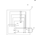
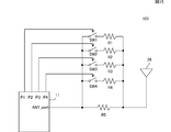
- FIG. 1 is a circuit diagram of a wireless communication apparatus 101 according to the first embodiment.
- FIG. 2 is an internal circuit diagram connected to the IO terminal 1a which is one of the IO terminals 11P of the RFIC 11.
- FIG. 3 is an equivalent circuit diagram of a variable impedance circuit connected to the antenna coil 13 and the capacitive element 14.
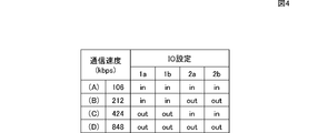
- FIG. 4 is a diagram showing the communication speed and the state of the IO terminal set correspondingly.
- 5A to 5D are equivalent circuit diagrams of the variable impedance circuit connected to the antenna coil 13 and the capacitive element 14 corresponding to the states (A) to (D) in FIG.
- FIG. 6 is a circuit diagram of the wireless communication apparatus 102 according to the second embodiment.
- FIG. 1 is a circuit diagram of a wireless communication apparatus 101 according to the first embodiment.
- FIG. 2 is an internal circuit diagram connected to the IO terminal 1a which is one of the IO terminals 11P of the RFIC 11.
- FIG. 3 is an equivalent circuit diagram of a
- FIG. 7 is a diagram illustrating the internal structure of the wireless communication device 103 according to the third embodiment, and is a plan view in a state where the lower housing 51 and the upper housing 52 are separated and the interior is exposed. It is.
- FIG. 8 is a diagram illustrating a structure inside the housing of the wireless communication device 104 according to the fourth embodiment, and is a plan view in a state where the lower housing 51 and the upper housing 52 are separated and the inside is exposed. It is.
- FIG. 9 is a circuit diagram of the main part of the wireless communication apparatus 104 according to the fourth embodiment.
- FIG. 10 is an exploded perspective view of the booster coil antenna 24 included in the wireless communication apparatus 104 according to the fourth embodiment.
- FIG. 11 is a cross-sectional view of a booster coil antenna portion formed integrally with the housing.
- FIG. 12 is an exploded perspective view of another booster coil antenna provided in the wireless communication apparatus 104 according to the fourth embodiment.
- FIG. 13 is an exploded perspective view of still another booster coil antenna included in the wireless communication apparatus 104 according to the fourth embodiment.
- FIG. 14 is a diagram illustrating a structure inside the housing of the wireless communication apparatus 105 according to the fifth embodiment, and is a plan view in a state where the lower housing 51 and the upper housing 52 are separated and the inside is exposed. It is.
- FIG. 15 is a circuit diagram of the main part of the wireless communication apparatus 105 according to the fifth embodiment.
- FIG. 1 is a circuit diagram of a main part of a wireless communication apparatus 101 according to the first embodiment.
- the wireless communication device 101 includes a resistance element built-in RFIC 110 and an antenna coil 13.
- the resistive element built-in RFIC 110 includes an RFIC (non-contact communication IC of the present invention) 11, a capacitive element 14, and resistive elements R1a, R1b, R2a, and R2b. Resistive elements R1a, R1b, R2a, R2b and a part of the circuit in RFIC 11 constitute a variable impedance circuit.
- the RFIC 11 includes GPIO (General Purpose Input / Output) IO terminals 11P (1a, 1b, 2a, 2b).
- GPIO General Purpose Input / Output
- RFIC 11 performs conversion between a baseband signal and a high-frequency signal.
- a control IC or the like is connected to the RFIC 11.
- the parallel circuit of the capacitive element 14 and the antenna coil 13 is connected to the two TX terminals (transmission signal terminals) Tx1 and Tx2 of the RFIC 11.
- the antenna coil 13 is connected to the terminals Tx1 and Tx2 of the RFIC 11, but the RFIC 11 performs not only transmission but also reception using the antenna coil 13 connected to the terminals Tx1 and Tx2.
- the IO terminal 11P (1a, 1b, 2a, 2b) of the RFIC 11 is connected to one end of the resistance elements R1a, R1b, R2a, R2b.
- the other ends of the resistance elements R1a, R1b, R2a, R2b are connected to either end of the antenna coil 13.
- resistance elements R1a, R1b, R2a, R2b may be chip resistors or resistance patterns formed on a circuit board.
- Capacitance element 14 constitutes an antenna circuit which is an LC parallel resonance circuit together with antenna coil 13, and sets the resonance frequency of the antenna circuit to a predetermined frequency.
- the antenna coil 13 performs electromagnetic wave coupling with an antenna of a communication partner to perform transmission / reception for near field communication.
- FIG. 2 is an internal circuit diagram connected to the IO terminal 1a which is one of the IO terminals 11P of the RFIC 11.
- the IO terminal of the RFIC 11 can be set to either input / output.
- the IO terminal 1a is set as an output port by the input / output control signal
- output data is output via the buffer BA1.
- the pull-up resistor PR enters the “50 ⁇ pull-up” state via the gate G1 by the resistance control signal.
- the input impedance of the buffer BA2 is very high, it is not affected by the connection of the buffer BA2.
- the pull-up resistor PR is brought into an “open” state via the gate G1 by the resistance control signal.
- the output of the buffer BA1 has a high impedance and is not affected by the connection of the buffer BA1.
- the pull-up resistor PR is set in the “50 ⁇ pull-up” state, so that the IO terminal 1a is grounded at 50 ⁇ in terms of high frequency.
- the IO terminal 1a becomes high impedance.
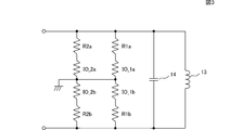
- FIG. 3 is an equivalent circuit diagram of a variable impedance circuit connected to the antenna coil 13 and the capacitive element 14.
- the resistor IO_1a represents a resistance value of a circuit portion connected to the IO terminal 1a formed in the RFIC 11 by a symbol of a resistance element.
- the resistor IO_1b represents a resistance value of a circuit portion connected to the IO terminal 1b, which is configured inside the RFIC 11, by a symbol of a resistance element.
- the resistor IO_2a is a circuit portion connected to the IO terminal 2a configured inside the RFIC 11
- the resistor IO_2b is a resistance value of the circuit portion connected to the IO terminal 2b configured inside the RFIC 11, respectively. It is a symbol.
- the resistor IO_1a becomes 50 ⁇ in terms of high frequency.
- the resistor IO_1a has a high impedance.
- FIG. 4 is a diagram showing the communication speed and the state of the IO terminal set correspondingly.
- “in” indicates a setting for an input port
- “out” indicates a setting for an output port.
- 5A to 5D are equivalent circuit diagrams of the variable impedance circuit connected to the antenna coil 13 and the capacitive element 14 corresponding to the states (A) to (D) in FIG.
- the resistance values of the resistance elements R1a, R1b, R2a, and R2b are set to values in the range of 1 k ⁇ to 10 k ⁇ , for example.
- the resistors IO_1a and IO_1b When communicating at a communication speed of 212 kbps, the resistors IO_1a and IO_1b have high impedance and the resistors IO_2a and IO_2b have 50 ⁇ as shown in the state (B). When communication is performed at a communication speed of 424 kbps, the resistors IO_1a and IO_1b are 50 ⁇ and the resistors IO_2a and IO_2b are high impedance as shown in the state (C).
- FIG. 4 is an example, and resistance values suitable for each of the four communication speeds (required bandwidth can be obtained) may be added (eight GPIO terminals are required).
- the relationship of R1a ⁇ R1b and R2a ⁇ R2b may be used.
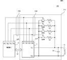
- FIG. 6 is a circuit diagram of the wireless communication apparatus 102 according to the second embodiment.
- the wireless communication device 102 is an example of an NFC module.
- the wireless communication device 102 includes a resistance element built-in RFIC 111, a control IC 12, and an antenna coil 13.
- the resistance element built-in RFIC 111 includes an RFIC (non-contact communication IC of the present invention) 11, a capacitor element 14, resistance elements R1, R2, R3, and R4 and switches SW1, SW2, SW3, and SW4. Resistive elements R1, R2, R3, R4 and switches SW1, SW2, SW3, SW4 constitute a variable impedance circuit.
- the RFIC 11 includes GPIO (General Purpose Input / Output) IO terminals 11P (P1, P2, P3, P4).
- the states of the switches SW1, SW2, SW3, SW4 are switched according to the output levels of these IO terminals.
- One ends of the resistance elements R1, R2, R3, and R4 are connected to one end of the antenna coil 13, and the other ends of the resistance elements R1, R2, R3, and R4 are connected to the switches SW1, SW2, SW3, and SW4. .
- the RFIC 11 performs conversion between a baseband signal and a high-frequency signal.
- the control IC 12 controls the RFIC 11 and inputs / outputs data including communication data.
- the parallel circuit of the capacitive element 14 and the antenna coil 13 is connected to the two TX terminals (transmission signal terminals) Tx1 and Tx2 of the RFIC 11.
- the IO terminal 11P of the RFIC 11 and the IO terminal 12P of the control IC 12 are connected by a signal line 15A.
- the RFIC 11 and the control IC 12 input and output communication signals via the data transmission line 16.
- the control IC 12 controls various settings of the RFIC 11 via the signal line 15A.
- the RFIC 11 and the control IC 12 are connected to the control terminals of the switches SW1, SW2, SW3, and SW4 via signal lines 15A and 15B.
- the state of the switches SW1, SW2, SW3, SW4 is switched by the output level of the IO terminals P1, P2, P3, P4 of the RFIC 11 by the circuit shown in FIG. Is switched. Similarly, the states of the switches SW1, SW2, SW3, and SW4 are switched depending on the output levels of the IO terminals P1, P2, P3, and P4 of the control IC 12, and the impedance of the additional circuit connected between both ends of the antenna coil 13 is switched. .
- resistance values of the resistance elements R1, R2, R3, and R4 are set to a power-of-two relationship, and binary code data is output from the IO terminals P1, P2, P3, and P4, they are added to the antenna circuit. Can be switched to a power of 2.
- FIG. 7 is a diagram illustrating the internal structure of the wireless communication device 103 according to the third embodiment, and is a plan view in a state where the lower housing 51 and the upper housing 52 are separated and the interior is exposed. It is.
- Printed wiring boards 21 and 31, a battery pack 33, and the like are housed inside the lower housing 51.
- An RFIC 11 and resistors R1a, R1b, R2a, and R2b are mounted on the printed wiring board 21.
- a UHF band antenna 22, a camera module 26, and the like are also mounted on the printed wiring board 21.
- the printed wiring board 31 is equipped with a UHF band antenna 32 and the like.
- the printed wiring board 21 and the printed wiring board 31 are connected via a coaxial cable 34.
- the antenna coil 13 is formed on the inner surface of the upper casing 52.
- the antenna coil 13 is a conductor patterned in a rectangular spiral shape. The end of the antenna coil 13 comes into contact with a pin terminal 25 provided on the printed wiring board 21 side and is electrically connected. That is, the antenna coil 13 is electrically connected to the RFIC 11 by covering the lower housing 51 with the upper housing 52.
- the antenna coil 13 is formed by MID (Molded Interconnect Device) technology using, for example, an LDS (Laser-Direct-Structuring) method. That is, a base polymer such as a liquid crystal polymer (LCP) or polybutylene terephthalate (PBT) is molded using a material in which a filler and an organic metal are mixed, and the molded product is irradiated with laser in the pattern of the antenna coil 13. The plating is deposited only on the laser irradiation part.
- LCP liquid crystal polymer
- PBT polybutylene terephthalate
- FIG. 8 is a diagram illustrating a structure inside the housing of the wireless communication device 104 according to the fourth embodiment, and is a plan view in a state where the lower housing 51 and the upper housing 52 are separated and the inside is exposed. It is.
- Printed wiring boards 21 and 31, a battery pack 33, and the like are housed inside the lower housing 51.
- An RFIC 11, resistors R1a, R1b, R2a, R2b, and a feeding coil 23 are mounted on the printed wiring board 21.
- a UHF band antenna 22, a camera module 26, and the like are also mounted on the printed wiring board 21.
- the printed wiring board 31 is equipped with a UHF band antenna 32 and the like.
- the printed wiring board 21 and the printed wiring board 31 are connected via a coaxial cable 34.
- a booster coil antenna 24 is formed on the inner surface of the upper casing 52. As will be described later, the booster coil antenna 24 is magnetically coupled to the feeding coil 23 and functions as a magnetic field antenna.
- FIG. 9 is a circuit diagram of the main part of the wireless communication apparatus 104 according to the fourth embodiment.
- the wireless communication device 104 includes an RFIC 11, a capacitive element 14, and resistive elements R1a, R1b, R2a, and R2b.
- a parallel circuit of the capacitive element 14 and the feeding coil 23 is connected between Tx1 and Tx2 of the RFIC 11.
- the booster coil antenna 24 is composed of a coil and a capacitive element, and the resonance frequency is determined by the inductance of the coil and the capacitance of the capacitive element.
- the coil of the booster coil antenna 24 is magnetically coupled to the feeding coil 23.
- FIG. 10 is an exploded perspective view of the booster coil antenna 24.
- the booster coil antenna 24 includes an insulating sheet 24S and coil conductors 24L1 and 24L2 formed on both sides thereof.
- the coil conductors 24L1 and 24L2 are conductors patterned in a rectangular spiral shape.
- the coil conductors 24L1, 24L2 are opposed to each other with the insulating sheet 24S interposed therebetween. And it is patterned so that capacitive coupling is performed in a state where current flows in the same direction in plan view.
- the coil conductors 24L1 and 24L2 are patterned so that when a clockwise current flows through the coil conductor 24L1 in a plan view from the same direction, a current also flows clockwise through the coil conductor 24L2.
- the capacitive coupling is represented by a capacitive element in the booster coil antenna 24 of FIG.
- the feeding coil 23 and the booster coil antenna 24 shown in FIG. 8 are arranged so that the magnetic flux is linked to both.
- FIG. 11 to FIG. 13 are diagrams relating to another configuration example of the booster coil antenna.
- FIG. 11 is a cross-sectional view of a booster coil antenna portion formed integrally with the housing.
- the coil conductors 24L1 and 24L2 are directly formed on both surfaces of the upper casing 52 by the LDS method or the like.
- FIG. 12 is an exploded perspective view of another booster coil antenna. In this example, it is composed of two insulating sheets 24S1, 24S2 and three coil conductors 24L1, 24L2, 24L3. These coil conductors 24L1, 24L2, and 24L3 are patterned so that a current in the same direction flows through each coil conductor in a plan view from the same direction.
- the coil conductor layer may be three or more layers.
- the booster coil antenna includes an insulating sheet 24S, a coil conductor 24L formed on one side, and a chip capacitor 24C.
- the LC resonance circuit may be configured using individual components to determine the resonance frequency.
- the RFIC 11, the resistance elements R1a, R1b, R2a, R2b and the feeding coil 23 are separately mounted on the printed wiring board.
- the resistance elements R1a, R1b, R2a, R2b may be mounted.
- the resistance elements R1a, R1b, R2a, and R2b are not limited to chip elements, and may be formed of a resistance pattern or a conductor pattern.
- FIG. 14 is a diagram illustrating a structure inside the housing of the wireless communication apparatus 105 according to the fifth embodiment, and is a plan view in a state where the lower housing 51 and the upper housing 52 are separated and the inside is exposed. It is.
- Printed wiring boards 21 and 31, a battery pack 33, and the like are housed inside the lower housing 51.
- An RFIC 11, a switch array ASW, and resistors R1a, R1b, R2a, and R2b are mounted on the printed wiring board 21.
- a conductor pattern of the antenna 26 is formed on the printed wiring board 21.
- the printed wiring board 21 is equipped with a UHF band antenna 22, a camera module 26, and the like.
- the printed wiring board 31 is equipped with a UHF band antenna 32 and the like.
- the printed wiring board 21 and the printed wiring board 31 are connected via a coaxial cable 34.
- FIG. 15 is a circuit diagram of the main part of the wireless communication apparatus 105 according to the fifth embodiment.
- the wireless communication device 105 includes an RFIC 11, switches SW1, SW2, SW3, and SW4 and resistance elements R1, R2, R3, R4, and R5.
- a field emission antenna 26 is connected to the antenna port ANT_port of the RFIC 11 via a resistor R5.
- the switches SW1, SW2, SW3, SW4 are provided in the switch array ASW shown in FIG.
- the resistance value between the antenna port ANT_port of the RFIC 11 and the antenna 26 is switched by the combination of the on / off states of the switches SW1 to SW4, and the Q value of the antenna is controlled. Thus, it can be applied to a field emission antenna.
- switches are used. However, the number of switches is not necessarily four. If fine adjustment is necessary, the number of switching may be increased, and if fine adjustment is unnecessary, three or less may be handled.
- the high-frequency device of the present invention is not limited to an RFID reader / writer, and may be configured as an RFID tag.
- the Q value of an antenna is controlled during transmission / reception has been described. Moreover, you may apply only to one at the time of transmission and reception. Furthermore, when the transmission and reception timings are separated, the Q value of the antenna may be different between transmission and reception.
- ASW Switch arrays BA1, BA2: Buffers G1, G2 ... Gates IO_1a, IO_1b, IO_2a, IO_2b ... Resistors P1, P2, P3, P4 ... IO terminals PR ... Pull-up resistors R1, R2, R3, R4 ... Resistive elements R1a, R1b, R2a, R2b ... Resistance elements SW1, SW2, SW3, SW4 ... Switches 1a, 1b, 2a, 2b ... IO terminals 11 ... RFIC 11P ... IO terminal 12 ... Control IC 12P ... IO terminal 13 ... antenna coil 14 ... capacitor elements 15A, 15B ... signal line 16 ... data transmission line 21, 31 ... printed wiring board 23 ... feed coil 24 ... booster coil antenna 26 ... antenna 33 ... battery pack 51 ... lower casing Body 52 ... Upper housing 101 to 105 ... Wireless communication device 110, 111 ... RFIC with built-in resistance element
Abstract
A wireless communication apparatus (101) is provided with an antenna coil (13), and an RFIC (110) having built-in resistive elements. The RFIC (110) is provided with an RFIC (11), a capacitive element (14), and resistive elements (R1a, R1b, R2a, R2b). A variable impedance circuit is configured of the resistive elements (R1a, R1b, R2a, R2b), and a part of a circuit in the RFIC (11). The RFIC (11) controls, depending on whether a predetermined IO terminal is set to an output port or to an input port, resistive circuit impedance to be added to an antenna circuit, and sets the Q value of the antenna circuit to a value that corresponds to a communication speed.
Description
本発明は、相手側機器と電磁界信号を介して通信するRFID(Radio Frequency Identification)システムや近距離無線通信(NFC:Near Field Communication)システムに用いられる無線通信装置に関するものである。
The present invention relates to a radio communication apparatus used in an RFID (Radio Frequency Identification) system or a near field communication (NFC) system that communicates with a counterpart device via an electromagnetic field signal.
NFCとは、非接触型識別技術と相互接続技術とを組み合わせた無線通信規格であり、この規格に準拠した装置同士は13.56MHz帯の周波数を使用し、数十cm程度の短い距離で双方向通信するというものである。NFCのシステムには複数の通信速度(106kbps,212kbps,424kbps,848kbps)が存在する。このため、最も高速の通信速度でも波形歪み無く通信できるようにするためには広帯域のアンテナが必要になる。
NFC is a wireless communication standard that combines contactless identification technology and interconnection technology, and devices that comply with this standard use a 13.56 MHz frequency band, and are bidirectional at short distances of several tens of centimeters. To communicate. NFC systems have multiple communication speeds (106kbps, 212kbps, 424kbps, 848kbps). For this reason, a broadband antenna is required to enable communication without waveform distortion even at the highest communication speed.
アンテナの広帯域化設計手法として、これまで特許文献1や特許文献2のように複数の共振回路を近接させ、複共振化させて広帯域化を図るという手法があった。
As a method for designing an antenna with a wider band, there has been a method of achieving a wider band by making a plurality of resonance circuits close to each other and making multiple resonances as in Patent Document 1 and Patent Document 2.
特許文献1や特許文献2のように、複数の共振回路を近接させて複共振化させる手法では、複数のLC共振回路を形成することが必須となるため、ある程度まとまったスペースを確保する必要があり、携帯端末などの小型の無線通信装置に組み込むことは困難であった。
In the method of making a plurality of resonance circuits close to each other as in Patent Document 1 and Patent Document 2, it is essential to form a plurality of LC resonance circuits, so it is necessary to secure a certain amount of space. Therefore, it has been difficult to incorporate it into a small wireless communication device such as a portable terminal.
また、単に広帯域特性のアンテナを用いるだけだと、低速通信時にはアンテナ効率を有効に利用できず、小型アンテナでは必要な通信距離が確保できない、ということにもなる。アンテナのQ値は、「Q = fo/B.W.」(但し、B.W.はアンテナの帯域幅、foは中心周波数である。)で表わされるので、一般的にはアンテナの帯域幅を広げるとQが劣化する。すなわち、広帯域特性を有するアンテナを用いる場合は、アンテナ自体が広帯域に設計されているため高速通信に適するが、帯域幅が狭くても問題のない低速通信時においては、Q値の悪い状態でアンテナを用いることになる。
Also, simply using a broadband antenna, the antenna efficiency cannot be used effectively during low-speed communication, and the required communication distance cannot be secured with a small antenna. Since the Q value of the antenna is expressed by “Q = fo / BW” (where BW is the bandwidth of the antenna and fo is the center frequency), in general, Q is degraded when the bandwidth of the antenna is widened. To do. That is, when an antenna having a wide band characteristic is used, it is suitable for high speed communication because the antenna itself is designed in a wide band. However, in low speed communication where there is no problem even if the bandwidth is narrow, the antenna has a poor Q value. Will be used.
そこで、本発明は、通信速度に応じて必要な帯域化を確保できる小型の無線通信装置を提供することを目的とするものである。
Therefore, an object of the present invention is to provide a small wireless communication apparatus capable of ensuring a necessary bandwidth according to the communication speed.
(1)本発明の無線通信装置は次のように構成される。
(1) The wireless communication apparatus of the present invention is configured as follows.
信号を送受信するための通信端子および複数のIO端子を備えた非接触通信用ICと、前記非接触通信用ICの前記通信端子に接続されたアンテナと、を備える無線通信装置において、
前記アンテナに、前記IO端子の状態に応じてインピーダンスが変わる可変インピーダンス回路が接続されたことを特徴とする。 In a wireless communication apparatus comprising: a non-contact communication IC having a communication terminal for transmitting and receiving a signal and a plurality of IO terminals; and an antenna connected to the communication terminal of the non-contact communication IC.
A variable impedance circuit whose impedance changes depending on the state of the IO terminal is connected to the antenna.
この構成により、非接触通信用ICのIO端子の状態に応じてアンテナに並列接続される可変インピーダンス回路のインピーダンスが設定され、アンテナ回路のQ値が適宜設定されて、必要な帯域幅が定められる。
With this configuration, the impedance of the variable impedance circuit connected in parallel to the antenna is set according to the state of the IO terminal of the non-contact communication IC, the Q value of the antenna circuit is appropriately set, and the necessary bandwidth is determined. .
(2)前記可変インピーダンス回路は、前記非接触通信用IC内に設けられ、前記IO端子とグランドとの間または前記IO端子と電源ラインとの間につながる回路と、前記IO端子と前記アンテナとの間に接続された抵抗素子とで構成されることが好ましい。
(2) The variable impedance circuit is provided in the non-contact communication IC, and is connected between the IO terminal and the ground or between the IO terminal and the power supply line, the IO terminal and the antenna. And a resistive element connected between them.
この構成により、非接触通信用ICの外部に接続する回路素子の数は少なくてすみ、簡素な回路で構成できる。
With this configuration, the number of circuit elements connected to the outside of the non-contact communication IC can be reduced, and a simple circuit can be configured.
(3)前記可変インピーダンス回路は、前記IO端子と前記アンテナとの間に接続され、前記IO端子の出力電圧で状態が切り替えられるスイッチと、このスイッチに直列接続された抵抗素子を含む回路であることが好ましい。
(3) The variable impedance circuit is a circuit including a switch connected between the IO terminal and the antenna, the state of which is switched by the output voltage of the IO terminal, and a resistance element connected in series to the switch. It is preferable.
この構成により、少ないIO端子数でアンテナ回路のQ値を多くの段階に切り替えることができる。
With this configuration, the Q value of the antenna circuit can be switched to many stages with a small number of IO terminals.
本発明によれば、非接触通信用ICのIO端子の状態に応じてアンテナに接続される可変インピーダンス回路のインピーダンスが設定されて、アンテナ回路のQ値が適宜設定され、通信速度に応じて必要な帯域が確保できる。そのため、複数のLC共振回路を形成する必要がなく、小型の無線通信装置が構成できる。
According to the present invention, the impedance of the variable impedance circuit connected to the antenna is set according to the state of the IO terminal of the non-contact communication IC, the Q value of the antenna circuit is appropriately set, and is necessary according to the communication speed. Secure bandwidth. Therefore, it is not necessary to form a plurality of LC resonance circuits, and a small wireless communication device can be configured.
《第1の実施形態》
図1は第1の実施形態に係る無線通信装置101の主要部の回路図である。この無線通信装置101は、抵抗素子内蔵RFIC110およびアンテナコイル13を備えている。抵抗素子内蔵RFIC110はRFIC(本発明の非接触通信用IC)11、容量素子14および抵抗素子R1a,R1b,R2a,R2bを備えている。抵抗素子R1a,R1b,R2a,R2bとRFIC11内の回路の一部とで可変インピーダンス回路が構成されている。 << First Embodiment >>
FIG. 1 is a circuit diagram of a main part of awireless communication apparatus 101 according to the first embodiment. The wireless communication device 101 includes a resistance element built-in RFIC 110 and an antenna coil 13. The resistive element built-in RFIC 110 includes an RFIC (non-contact communication IC of the present invention) 11, a capacitive element 14, and resistive elements R1a, R1b, R2a, and R2b. Resistive elements R1a, R1b, R2a, R2b and a part of the circuit in RFIC 11 constitute a variable impedance circuit.
図1は第1の実施形態に係る無線通信装置101の主要部の回路図である。この無線通信装置101は、抵抗素子内蔵RFIC110およびアンテナコイル13を備えている。抵抗素子内蔵RFIC110はRFIC(本発明の非接触通信用IC)11、容量素子14および抵抗素子R1a,R1b,R2a,R2bを備えている。抵抗素子R1a,R1b,R2a,R2bとRFIC11内の回路の一部とで可変インピーダンス回路が構成されている。 << First Embodiment >>
FIG. 1 is a circuit diagram of a main part of a
RFIC11はGPIO(General Purpose Input/Output)のIO端子11P(1a,1b,2a,2b)を備えている。
The RFIC 11 includes GPIO (General Purpose Input / Output) IO terminals 11P (1a, 1b, 2a, 2b).
RFIC11はベースバンド信号と高周波信号との間の変換を行う。このRFIC11には制御IC等が接続される。
RFIC 11 performs conversion between a baseband signal and a high-frequency signal. A control IC or the like is connected to the RFIC 11.
RFIC11の2つのTX端子(送信信号端子)Tx1,Tx2に容量素子14およびアンテナコイル13の並列回路が接続されている。なお、アンテナコイル13はRFIC11の端子Tx1,Tx2に接続されているが、RFIC11は端子Tx1,Tx2に接続されているアンテナコイル13を用いて送信だけでなく受信も行う。
The parallel circuit of the capacitive element 14 and the antenna coil 13 is connected to the two TX terminals (transmission signal terminals) Tx1 and Tx2 of the RFIC 11. The antenna coil 13 is connected to the terminals Tx1 and Tx2 of the RFIC 11, but the RFIC 11 performs not only transmission but also reception using the antenna coil 13 connected to the terminals Tx1 and Tx2.
RFIC11のIO端子11P(1a,1b,2a,2b)は抵抗素子R1a,R1b,R2a,R2bの一方端に接続されている。抵抗素子R1a,R1b,R2a,R2bの他方端はアンテナコイル13の両端のいずれかに接続されている。
The IO terminal 11P (1a, 1b, 2a, 2b) of the RFIC 11 is connected to one end of the resistance elements R1a, R1b, R2a, R2b. The other ends of the resistance elements R1a, R1b, R2a, R2b are connected to either end of the antenna coil 13.
これらの抵抗素子R1a,R1b,R2a,R2bは、チップ抵抗であってもよいし、回路基板上に形成された抵抗パターンであってもよい。
These resistance elements R1a, R1b, R2a, R2b may be chip resistors or resistance patterns formed on a circuit board.
容量素子14はアンテナコイル13とともにLC並列共振回路であるアンテナ回路を構成し、アンテナ回路の共振周波数を所定周波数に定める。アンテナコイル13は通信相手のアンテナと電磁界結合して近距離通信のための送受信を行う。
Capacitance element 14 constitutes an antenna circuit which is an LC parallel resonance circuit together with antenna coil 13, and sets the resonance frequency of the antenna circuit to a predetermined frequency. The antenna coil 13 performs electromagnetic wave coupling with an antenna of a communication partner to perform transmission / reception for near field communication.
図2は、前記RFIC11のIO端子11Pの1つであるIO端子1aにつながる内部の回路図である。この例では、RFIC11のIO端子は入力/出力のいずれにも設定できる。入出力制御信号によってIO端子1aが出力ポートとして設定されると、バッファBA1を介して出力データが出力される。このとき、抵抗制御信号によってゲートG1を介してプルアップ抵抗PRが「50Ωプルアップ」状態になる。また、バッファBA2の入力インピーダンスは非常に高いので、バッファBA2が接続されていることの影響は受けない。IO端子1aが入力ポートとして設定されると、バッファBA2、ゲートG2を介して入力データが取り込まれる。このとき、抵抗制御信号によってゲートG1を介してプルアップ抵抗PRが「オープン」状態になる。また、バッファBA1の出力は高インピーダンスとなり、バッファBA1が接続されていることの影響を受けない。
FIG. 2 is an internal circuit diagram connected to the IO terminal 1a which is one of the IO terminals 11P of the RFIC 11. In this example, the IO terminal of the RFIC 11 can be set to either input / output. When the IO terminal 1a is set as an output port by the input / output control signal, output data is output via the buffer BA1. At this time, the pull-up resistor PR enters the “50Ω pull-up” state via the gate G1 by the resistance control signal. Also, since the input impedance of the buffer BA2 is very high, it is not affected by the connection of the buffer BA2. When the IO terminal 1a is set as an input port, input data is taken in via the buffer BA2 and the gate G2. At this time, the pull-up resistor PR is brought into an “open” state via the gate G1 by the resistance control signal. Further, the output of the buffer BA1 has a high impedance and is not affected by the connection of the buffer BA1.
したがって、IOポート1aが出力ポートに設定されると、プルアップ抵抗PRが「50Ωプルアップ」状態に設定されるので、IO端子1aは高周波的には50Ωで接地される。IOポート1aが入力ポートに設定されると、IO端子1aは高インピーダンスとなる。
Therefore, when the IO port 1a is set as an output port, the pull-up resistor PR is set in the “50Ω pull-up” state, so that the IO terminal 1a is grounded at 50Ω in terms of high frequency. When the IO port 1a is set as an input port, the IO terminal 1a becomes high impedance.
図3は、アンテナコイル13および容量素子14に接続された可変インピーダンス回路の等価回路図である。ここで抵抗IO_1aは、RFIC11の内部に構成された、IO端子1aにつながる回路部分による抵抗値を抵抗素子の記号で表したものである。抵抗IO_1bは、RFIC11の内部に構成された、IO端子1bにつながる回路部分による抵抗値を抵抗素子の記号で表したものである。同様に、抵抗IO_2aは、RFIC11の内部に構成された、IO端子2aにつながる回路部分、抵抗IO_2bは、RFIC11の内部に構成された、IO端子2bにつながる回路部分による抵抗値をそれぞれ抵抗素子の記号で表したものである。
FIG. 3 is an equivalent circuit diagram of a variable impedance circuit connected to the antenna coil 13 and the capacitive element 14. Here, the resistor IO_1a represents a resistance value of a circuit portion connected to the IO terminal 1a formed in the RFIC 11 by a symbol of a resistance element. The resistor IO_1b represents a resistance value of a circuit portion connected to the IO terminal 1b, which is configured inside the RFIC 11, by a symbol of a resistance element. Similarly, the resistor IO_2a is a circuit portion connected to the IO terminal 2a configured inside the RFIC 11, and the resistor IO_2b is a resistance value of the circuit portion connected to the IO terminal 2b configured inside the RFIC 11, respectively. It is a symbol.
図2に示したように、例えばIO端子1aが出力ポートに設定されると、前記抵抗IO_1aは高周波的に50Ωとなる。IO端子1aが入力ポートとして設定されると、前記抵抗IO_1aは高インピーダンスとなる。
As shown in FIG. 2, for example, when the IO terminal 1a is set as an output port, the resistor IO_1a becomes 50Ω in terms of high frequency. When the IO terminal 1a is set as an input port, the resistor IO_1a has a high impedance.
図3に示したその他の抵抗IO_1b,IO_2a,IO_2bについても同様である。
The same applies to the other resistors IO_1b, IO_2a, and IO_2b shown in FIG.
図4は通信速度と、それに対応して設定するIO端子の状態を示す図である。図中“in”は入力ポートへの設定、“out”は出力ポートへの設定をそれぞれ表れている。また、図5(A)~(D)は図4中の状態(A)~(D)に対応する、アンテナコイル13および容量素子14に接続された可変インピーダンス回路の等価回路図である。
FIG. 4 is a diagram showing the communication speed and the state of the IO terminal set correspondingly. In the figure, “in” indicates a setting for an input port, and “out” indicates a setting for an output port. 5A to 5D are equivalent circuit diagrams of the variable impedance circuit connected to the antenna coil 13 and the capacitive element 14 corresponding to the states (A) to (D) in FIG.
抵抗素子R1a,R1b,R2a,R2bの各抵抗値を同じ記号で表すと、
R1a=R1b<R2a=R2bの関係にある。抵抗素子R1a,R1b,R2a,R2bの抵抗値は例えば1kΩ~10kΩの範囲内の値とする。 When the resistance values of the resistance elements R1a, R1b, R2a, R2b are represented by the same symbol,
R1a = R1b <R2a = R2b. The resistance values of the resistance elements R1a, R1b, R2a, and R2b are set to values in the range of 1 kΩ to 10 kΩ, for example.
通信速度106kbpsで通信される場合、図4の状態(A)で示すように、抵抗IO_1a,IO_1b,IO_2a,IO_2bのすべてが高インピーダンスになり、アンテナ回路のQ値は最も高く、帯域幅は最も狭くなる。通信速度848kbpsで通信される場合、状態(D)で示すように、抵抗IO_1a,IO_1b,IO_2a,IO_2bのすべてが50Ωになり、アンテナ回路のQ値は最も低く、帯域幅は最も広くなる。通信速度212kbpsで通信される場合、状態(B)で示すように、抵抗IO_1a,IO_1bが高インピーダンス、抵抗IO_2a,IO_2bが50Ωになる。通信速度424kbpsで通信される場合、状態(C)で示すように、抵抗IO_1a,IO_1bが50Ω、抵抗IO_2a,IO_2bが高インピーダンスになる。
When communicating at a communication speed of 106 kbps, as shown in the state (A) of FIG. 4, all of the resistors IO_1a, IO_1b, IO_2a, and IO_2b have high impedance, the Q value of the antenna circuit is the highest, and the bandwidth is the highest. Narrow. When communication is performed at a communication speed of 848 kbps, as shown in the state (D), all of the resistors IO_1a, IO_1b, IO_2a, and IO_2b are 50Ω, and the Q value of the antenna circuit is the lowest and the bandwidth is the widest. When communicating at a communication speed of 212 kbps, the resistors IO_1a and IO_1b have high impedance and the resistors IO_2a and IO_2b have 50Ω as shown in the state (B). When communication is performed at a communication speed of 424 kbps, the resistors IO_1a and IO_1b are 50Ω and the resistors IO_2a and IO_2b are high impedance as shown in the state (C).
なお、図4は一例であって、4つの通信速度それぞれに合う(必要帯域幅が得られる)抵抗値をそれぞれ付加してもよい(GPIO端子は8つ必要)。また、上図でR1a≠R1b,R2a≠R2bの関係であってもよい。
Note that FIG. 4 is an example, and resistance values suitable for each of the four communication speeds (required bandwidth can be obtained) may be added (eight GPIO terminals are required). In the upper diagram, the relationship of R1a ≠ R1b and R2a ≠ R2b may be used.
《第2の実施形態》
図6は第2の実施形態に係る無線通信装置102の回路図である。この無線通信装置102はNFCモジュールの一例である。無線通信装置102は、抵抗素子内蔵RFIC111、制御IC12およびアンテナコイル13を備えている。抵抗素子内蔵RFIC111は、RFIC(本発明の非接触通信用IC)11、容量素子14、抵抗素子R1,R2,R3,R4およびスイッチSW1,SW2,SW3,SW4を備えている。抵抗素子R1,R2,R3,R4とスイッチSW1,SW2,SW3,SW4とで可変インピーダンス回路が構成されている。 << Second Embodiment >>
FIG. 6 is a circuit diagram of thewireless communication apparatus 102 according to the second embodiment. The wireless communication device 102 is an example of an NFC module. The wireless communication device 102 includes a resistance element built-in RFIC 111, a control IC 12, and an antenna coil 13. The resistance element built-in RFIC 111 includes an RFIC (non-contact communication IC of the present invention) 11, a capacitor element 14, resistance elements R1, R2, R3, and R4 and switches SW1, SW2, SW3, and SW4. Resistive elements R1, R2, R3, R4 and switches SW1, SW2, SW3, SW4 constitute a variable impedance circuit.
図6は第2の実施形態に係る無線通信装置102の回路図である。この無線通信装置102はNFCモジュールの一例である。無線通信装置102は、抵抗素子内蔵RFIC111、制御IC12およびアンテナコイル13を備えている。抵抗素子内蔵RFIC111は、RFIC(本発明の非接触通信用IC)11、容量素子14、抵抗素子R1,R2,R3,R4およびスイッチSW1,SW2,SW3,SW4を備えている。抵抗素子R1,R2,R3,R4とスイッチSW1,SW2,SW3,SW4とで可変インピーダンス回路が構成されている。 << Second Embodiment >>
FIG. 6 is a circuit diagram of the
RFIC11はGPIO(General Purpose Input/Output)のIO端子11P(P1,P2,P3,P4)を備えている。これらのIO端子の出力レベルによってスイッチSW1,SW2,SW3,SW4の状態が切り替えられる。抵抗素子R1,R2,R3,R4の一方端はアンテナコイル13の一端に接続されていて、抵抗素子R1,R2,R3,R4の他端はスイッチSW1,SW2,SW3,SW4に接続されている。
The RFIC 11 includes GPIO (General Purpose Input / Output) IO terminals 11P (P1, P2, P3, P4). The states of the switches SW1, SW2, SW3, SW4 are switched according to the output levels of these IO terminals. One ends of the resistance elements R1, R2, R3, and R4 are connected to one end of the antenna coil 13, and the other ends of the resistance elements R1, R2, R3, and R4 are connected to the switches SW1, SW2, SW3, and SW4. .
RFIC11はベースバンド信号と高周波信号との間の変換を行う。制御IC12は、RFIC11を制御し、通信データを含むデータを入出力する。
RFIC 11 performs conversion between a baseband signal and a high-frequency signal. The control IC 12 controls the RFIC 11 and inputs / outputs data including communication data.
RFIC11の2つのTX端子(送信信号端子)Tx1,Tx2に容量素子14およびアンテナコイル13の並列回路が接続されている。
The parallel circuit of the capacitive element 14 and the antenna coil 13 is connected to the two TX terminals (transmission signal terminals) Tx1 and Tx2 of the RFIC 11.
RFIC11のIO端子11Pおよび制御IC12のIO端子12Pは信号ライン15Aで接続されている。
The IO terminal 11P of the RFIC 11 and the IO terminal 12P of the control IC 12 are connected by a signal line 15A.
RFIC11と制御IC12とはデータ伝送ライン16を介して通信信号の入出力を行い。制御IC12は信号ライン15Aを介してRFIC11の各種設定などの制御を行う。また、RFIC11および制御IC12は信号ライン15A,15Bを介してスイッチSW1,SW2,SW3,SW4の制御端子に接続されている。
The RFIC 11 and the control IC 12 input and output communication signals via the data transmission line 16. The control IC 12 controls various settings of the RFIC 11 via the signal line 15A. The RFIC 11 and the control IC 12 are connected to the control terminals of the switches SW1, SW2, SW3, and SW4 via signal lines 15A and 15B.
図6に示した回路によって、RFIC11のIO端子P1,P2,P3,P4の出力レベルによってスイッチSW1,SW2,SW3,SW4の状態が切り替えられ、アンテナコイル13両端間に接続される付加回路のインピーダンスが切り替えられる。同様に、制御IC12のIO端子P1,P2,P3,P4の出力レベルによってもスイッチSW1,SW2,SW3,SW4の状態が切り替えられ、アンテナコイル13両端間に接続される付加回路のインピーダンスが切り替えられる。
The state of the switches SW1, SW2, SW3, SW4 is switched by the output level of the IO terminals P1, P2, P3, P4 of the RFIC 11 by the circuit shown in FIG. Is switched. Similarly, the states of the switches SW1, SW2, SW3, and SW4 are switched depending on the output levels of the IO terminals P1, P2, P3, and P4 of the control IC 12, and the impedance of the additional circuit connected between both ends of the antenna coil 13 is switched. .
抵抗素子R1,R2,R3,R4の抵抗値を適宜定めておくことで、アンテナコイル13両端間に接続される付加回路のインピーダンスを設定でき、これによって、アンテナ回路のQ値を通信速度に適した値に設定できる。
By appropriately determining the resistance values of the resistance elements R1, R2, R3, and R4, it is possible to set the impedance of the additional circuit connected between both ends of the antenna coil 13, thereby making the Q value of the antenna circuit suitable for the communication speed. Value can be set.
なお、抵抗素子R1,R2,R3,R4の抵抗値を2のべき乗の関係としておき、IO端子P1,P2,P3,P4から二進符号のデータを出力するようにすれば、アンテナ回路に付加されるインピーダンスを2のべき乗通りに切り替えることができる。
If the resistance values of the resistance elements R1, R2, R3, and R4 are set to a power-of-two relationship, and binary code data is output from the IO terminals P1, P2, P3, and P4, they are added to the antenna circuit. Can be switched to a power of 2.
《第3の実施形態》
図7は第3の実施形態に係る無線通信装置103の筐体内部の構造を示す図であり、下部筐体51と上部筐体52とを分離して内部を露出させた状態での平面図である。下部筐体51の内部にはプリント配線板21,31、バッテリーパック33等が収められている。プリント配線板21にはRFIC11、抵抗R1a,R1b,R2a,R2bが実装されている。このプリント配線板21にはUHF帯アンテナ22、カメラモジュール26等も搭載されている。また、プリント配線板31にはUHF帯アンテナ32等が搭載されている。プリント配線板21とプリント配線板31とは同軸ケーブル34を介して接続されている。 << Third Embodiment >>
FIG. 7 is a diagram illustrating the internal structure of thewireless communication device 103 according to the third embodiment, and is a plan view in a state where the lower housing 51 and the upper housing 52 are separated and the interior is exposed. It is. Printed wiring boards 21 and 31, a battery pack 33, and the like are housed inside the lower housing 51. An RFIC 11 and resistors R1a, R1b, R2a, and R2b are mounted on the printed wiring board 21. A UHF band antenna 22, a camera module 26, and the like are also mounted on the printed wiring board 21. The printed wiring board 31 is equipped with a UHF band antenna 32 and the like. The printed wiring board 21 and the printed wiring board 31 are connected via a coaxial cable 34.
図7は第3の実施形態に係る無線通信装置103の筐体内部の構造を示す図であり、下部筐体51と上部筐体52とを分離して内部を露出させた状態での平面図である。下部筐体51の内部にはプリント配線板21,31、バッテリーパック33等が収められている。プリント配線板21にはRFIC11、抵抗R1a,R1b,R2a,R2bが実装されている。このプリント配線板21にはUHF帯アンテナ22、カメラモジュール26等も搭載されている。また、プリント配線板31にはUHF帯アンテナ32等が搭載されている。プリント配線板21とプリント配線板31とは同軸ケーブル34を介して接続されている。 << Third Embodiment >>
FIG. 7 is a diagram illustrating the internal structure of the
上部筐体52の内面にはアンテナコイル13が形成されている。このアンテナコイル13は矩形渦巻状にパターン化された導体である。このアンテナコイル13の端部はプリント配線板21側に設けられたピン端子25に当接して電気的に導通する。すなわち、下部筐体51に上部筐体52を被せることで、アンテナコイル13はRFIC11に電気的に接続される。
The antenna coil 13 is formed on the inner surface of the upper casing 52. The antenna coil 13 is a conductor patterned in a rectangular spiral shape. The end of the antenna coil 13 comes into contact with a pin terminal 25 provided on the printed wiring board 21 side and is electrically connected. That is, the antenna coil 13 is electrically connected to the RFIC 11 by covering the lower housing 51 with the upper housing 52.
前記アンテナコイル13は例えばLDS(Laser-Direct-Structuring)法を用いたMID(Molded Interconnect Device)技術で形成する。すなわち、液晶ポリマー(LCP)やポリブチレンテレフタレート(PBT)等のベースポリマーにフィラー、有機金属を混ぜ合わせた材料を使用して成型し、その成型品にアンテナコイル13のパターン状にレーザ照射を行い、レーザ照射部のみにメッキを析出させる。
The antenna coil 13 is formed by MID (Molded Interconnect Device) technology using, for example, an LDS (Laser-Direct-Structuring) method. That is, a base polymer such as a liquid crystal polymer (LCP) or polybutylene terephthalate (PBT) is molded using a material in which a filler and an organic metal are mixed, and the molded product is irradiated with laser in the pattern of the antenna coil 13. The plating is deposited only on the laser irradiation part.
なお、筺体にアンテナコイルを直接描画する工法以外に、アンテナコイルを形成したフレキシブル基板を筐体に両面粘着シートを介して貼付する工法であってもよい
《第4の実施形態》
図8は第4の実施形態に係る無線通信装置104の筐体内部の構造を示す図であり、下部筐体51と上部筐体52とを分離して内部を露出させた状態での平面図である。下部筐体51の内部にはプリント配線板21,31、バッテリーパック33等が収められている。プリント配線板21にはRFIC11、抵抗R1a,R1b,R2a,R2b、給電コイル23が実装されている。このプリント配線板21にはUHF帯アンテナ22、カメラモジュール26等も搭載されている。また、プリント配線板31にはUHF帯アンテナ32等が搭載されている。プリント配線板21とプリント配線板31とは同軸ケーブル34を介して接続されている。 In addition to the method of drawing the antenna coil directly on the housing, a method of attaching the flexible substrate on which the antenna coil is formed to the housing via a double-sided adhesive sheet may be used.
FIG. 8 is a diagram illustrating a structure inside the housing of thewireless communication device 104 according to the fourth embodiment, and is a plan view in a state where the lower housing 51 and the upper housing 52 are separated and the inside is exposed. It is. Printed wiring boards 21 and 31, a battery pack 33, and the like are housed inside the lower housing 51. An RFIC 11, resistors R1a, R1b, R2a, R2b, and a feeding coil 23 are mounted on the printed wiring board 21. A UHF band antenna 22, a camera module 26, and the like are also mounted on the printed wiring board 21. The printed wiring board 31 is equipped with a UHF band antenna 32 and the like. The printed wiring board 21 and the printed wiring board 31 are connected via a coaxial cable 34.
《第4の実施形態》
図8は第4の実施形態に係る無線通信装置104の筐体内部の構造を示す図であり、下部筐体51と上部筐体52とを分離して内部を露出させた状態での平面図である。下部筐体51の内部にはプリント配線板21,31、バッテリーパック33等が収められている。プリント配線板21にはRFIC11、抵抗R1a,R1b,R2a,R2b、給電コイル23が実装されている。このプリント配線板21にはUHF帯アンテナ22、カメラモジュール26等も搭載されている。また、プリント配線板31にはUHF帯アンテナ32等が搭載されている。プリント配線板21とプリント配線板31とは同軸ケーブル34を介して接続されている。 In addition to the method of drawing the antenna coil directly on the housing, a method of attaching the flexible substrate on which the antenna coil is formed to the housing via a double-sided adhesive sheet may be used.
FIG. 8 is a diagram illustrating a structure inside the housing of the
上部筐体52の内面にはブースターコイルアンテナ24が形成されている。このブースターコイルアンテナ24は後に示すように給電コイル23と磁気的に結合し、磁界アンテナとして作用する。
A booster coil antenna 24 is formed on the inner surface of the upper casing 52. As will be described later, the booster coil antenna 24 is magnetically coupled to the feeding coil 23 and functions as a magnetic field antenna.
図9は第4の実施形態に係る無線通信装置104の主要部の回路図である。この無線通信装置104は、RFIC11、容量素子14および抵抗素子R1a,R1b,R2a,R2bを備えている。RFIC11のTx1,Tx2間に容量素子14および給電コイル23の並列回路が接続されている。ブースターコイルアンテナ24はコイルと容量素子とで構成されていて、このコイルのインダクタンスと容量素子のキャパシタンスとで共振周波数が定められている。このブースターコイルアンテナ24のコイルは給電コイル23と磁気的に結合する。
FIG. 9 is a circuit diagram of the main part of the wireless communication apparatus 104 according to the fourth embodiment. The wireless communication device 104 includes an RFIC 11, a capacitive element 14, and resistive elements R1a, R1b, R2a, and R2b. A parallel circuit of the capacitive element 14 and the feeding coil 23 is connected between Tx1 and Tx2 of the RFIC 11. The booster coil antenna 24 is composed of a coil and a capacitive element, and the resonance frequency is determined by the inductance of the coil and the capacitance of the capacitive element. The coil of the booster coil antenna 24 is magnetically coupled to the feeding coil 23.
図10はブースターコイルアンテナ24の分解斜視図である。このブースターコイルアンテナ24は絶縁性シート24Sおよびこの両面に形成されたコイル導体24L1,24L2で構成されている。コイル導体24L1,24L2はそれぞれ矩形渦巻状にパターン化された導体である。コイル導体24L1,24L2は絶縁シート24Sを挟んで対向している。そして、平面視で同方向に電流が流れる状態で容量結合するようにパターン化されている。同一方向からの平面視で、コイル導体24L1に時計回りの電流が流れるとき、コイル導体24L2にも時計回りに電流が流れるように、コイル導体24L1,24L2はパターン化されている。前記容量結合を図9のブースターコイルアンテナ24内では容量素子で表している。
FIG. 10 is an exploded perspective view of the booster coil antenna 24. The booster coil antenna 24 includes an insulating sheet 24S and coil conductors 24L1 and 24L2 formed on both sides thereof. The coil conductors 24L1 and 24L2 are conductors patterned in a rectangular spiral shape. The coil conductors 24L1, 24L2 are opposed to each other with the insulating sheet 24S interposed therebetween. And it is patterned so that capacitive coupling is performed in a state where current flows in the same direction in plan view. The coil conductors 24L1 and 24L2 are patterned so that when a clockwise current flows through the coil conductor 24L1 in a plan view from the same direction, a current also flows clockwise through the coil conductor 24L2. The capacitive coupling is represented by a capacitive element in the booster coil antenna 24 of FIG.
図8に示した給電コイル23およびブースターコイルアンテナ24は両者に磁束が鎖交するように配置されている。
The feeding coil 23 and the booster coil antenna 24 shown in FIG. 8 are arranged so that the magnetic flux is linked to both.
図11~図13はそれぞれブースターコイルアンテナの別の構成例に関する図である。図11は筐体に一体的に形成したブースターコイルアンテナ部分の断面図である。これは、上部筐体52の両面にコイル導体24L1,24L2をLDS法などによって直接形成したものである。図12は別のブースターコイルアンテナの分解斜視図である。この例では、2つの絶縁性シート24S1,24S2および3つのコイル導体24L1,24L2,24L3で構成されている。これらのコイル導体24L1,24L2,24L3は、同一方向からの平面視で、各コイル導体に同方向の電流が流れるようにパターン化されている。このようにコイル導体層は3層以上であってもよい。図13はさらに別のブースターコイルアンテナの分解斜視図である。このブースターコイルアンテナは、絶縁性シート24S、この片面に形成されたコイル導体24Lおよびチップコンデンサ24Cで構成されている。このように個別部品を用いてLC共振回路を構成し、共振周波数を定めてもよい。
FIG. 11 to FIG. 13 are diagrams relating to another configuration example of the booster coil antenna. FIG. 11 is a cross-sectional view of a booster coil antenna portion formed integrally with the housing. In this case, the coil conductors 24L1 and 24L2 are directly formed on both surfaces of the upper casing 52 by the LDS method or the like. FIG. 12 is an exploded perspective view of another booster coil antenna. In this example, it is composed of two insulating sheets 24S1, 24S2 and three coil conductors 24L1, 24L2, 24L3. These coil conductors 24L1, 24L2, and 24L3 are patterned so that a current in the same direction flows through each coil conductor in a plan view from the same direction. Thus, the coil conductor layer may be three or more layers. FIG. 13 is an exploded perspective view of still another booster coil antenna. The booster coil antenna includes an insulating sheet 24S, a coil conductor 24L formed on one side, and a chip capacitor 24C. In this way, the LC resonance circuit may be configured using individual components to determine the resonance frequency.
なお、図8に示した例では、RFIC11、抵抗素子R1a,R1b,R2a,R2bおよび給電コイル23をプリント配線板上に別々に実装したが、給電コイル23上に抵抗素子R1a,R1b,R2a,R2bを実装してもよい。また、抵抗素子R1a,R1b,R2a,R2bはチップ素子に限らず、抵抗パターンや導体パターンで形成してもよい。
In the example shown in FIG. 8, the RFIC 11, the resistance elements R1a, R1b, R2a, R2b and the feeding coil 23 are separately mounted on the printed wiring board. However, the resistance elements R1a, R1b, R2a, R2b may be mounted. Further, the resistance elements R1a, R1b, R2a, and R2b are not limited to chip elements, and may be formed of a resistance pattern or a conductor pattern.
《第5の実施形態》
図14は第5の実施形態に係る無線通信装置105の筐体内部の構造を示す図であり、下部筐体51と上部筐体52とを分離して内部を露出させた状態での平面図である。下部筐体51の内部にはプリント配線板21,31、バッテリーパック33等が収められている。プリント配線板21にはRFIC11、スイッチアレイASW、および抵抗R1a,R1b,R2a,R2bが実装されている。プリント配線板21にはアンテナ26の導体パターンが形成されている。また、このプリント配線板21にはUHF帯アンテナ22、カメラモジュール26等が搭載されている。また、プリント配線板31にはUHF帯アンテナ32等が搭載されている。プリント配線板21とプリント配線板31とは同軸ケーブル34を介して接続されている。 << Fifth Embodiment >>
FIG. 14 is a diagram illustrating a structure inside the housing of thewireless communication apparatus 105 according to the fifth embodiment, and is a plan view in a state where the lower housing 51 and the upper housing 52 are separated and the inside is exposed. It is. Printed wiring boards 21 and 31, a battery pack 33, and the like are housed inside the lower housing 51. An RFIC 11, a switch array ASW, and resistors R1a, R1b, R2a, and R2b are mounted on the printed wiring board 21. A conductor pattern of the antenna 26 is formed on the printed wiring board 21. The printed wiring board 21 is equipped with a UHF band antenna 22, a camera module 26, and the like. The printed wiring board 31 is equipped with a UHF band antenna 32 and the like. The printed wiring board 21 and the printed wiring board 31 are connected via a coaxial cable 34.
図14は第5の実施形態に係る無線通信装置105の筐体内部の構造を示す図であり、下部筐体51と上部筐体52とを分離して内部を露出させた状態での平面図である。下部筐体51の内部にはプリント配線板21,31、バッテリーパック33等が収められている。プリント配線板21にはRFIC11、スイッチアレイASW、および抵抗R1a,R1b,R2a,R2bが実装されている。プリント配線板21にはアンテナ26の導体パターンが形成されている。また、このプリント配線板21にはUHF帯アンテナ22、カメラモジュール26等が搭載されている。また、プリント配線板31にはUHF帯アンテナ32等が搭載されている。プリント配線板21とプリント配線板31とは同軸ケーブル34を介して接続されている。 << Fifth Embodiment >>
FIG. 14 is a diagram illustrating a structure inside the housing of the
図15は第5の実施形態に係る無線通信装置105の主要部の回路図である。この無線通信装置105は、RFIC11、スイッチSW1,SW2,SW3,SW4および抵抗素子R1,R2,R3,R4,R5を備えている。RFIC11のアンテナポートANT_portに抵抗R5を介して電界放射型アンテナ26が接続されている。スイッチSW1,SW2,SW3,SW4は図14に示したスイッチアレイASWに設けられている。
FIG. 15 is a circuit diagram of the main part of the wireless communication apparatus 105 according to the fifth embodiment. The wireless communication device 105 includes an RFIC 11, switches SW1, SW2, SW3, and SW4 and resistance elements R1, R2, R3, R4, and R5. A field emission antenna 26 is connected to the antenna port ANT_port of the RFIC 11 via a resistor R5. The switches SW1, SW2, SW3, SW4 are provided in the switch array ASW shown in FIG.
スイッチSW1~SW4のオン/オフ状態の組み合わせによって、RFIC11のアンテナポートANT_portとアンテナ26との間の抵抗値が切り替えられ、アンテナのQ値が制御される。このように、電界放射型アンテナにも適用できる。
The resistance value between the antenna port ANT_port of the RFIC 11 and the antenna 26 is switched by the combination of the on / off states of the switches SW1 to SW4, and the Q value of the antenna is controlled. Thus, it can be applied to a field emission antenna.
なお、図15に示した例では4つのスイッチを用いたが、必ずしも4つである必要は無い。微調整が必要であれば切り替え数を増やすとよいし、微調整が不要であれば3つ以下で対応してもよい。
In the example shown in FIG. 15, four switches are used. However, the number of switches is not necessarily four. If fine adjustment is necessary, the number of switching may be increased, and if fine adjustment is unnecessary, three or less may be handled.
《他の実施形態》
以上、本発明を具体的な実施の形態について説明したが、本発明はこの例に限定されるものではない。 << Other embodiments >>
While the present invention has been described with respect to specific embodiments, the present invention is not limited to this example.
以上、本発明を具体的な実施の形態について説明したが、本発明はこの例に限定されるものではない。 << Other embodiments >>
While the present invention has been described with respect to specific embodiments, the present invention is not limited to this example.
例えば、本発明の高周波デバイスは、RFIDのリーダライタに限定されるものではなく、RFIDタグとして構成されていてもよい。また、各実施形態では、送受信時にアンテナのQ値を制御する例を示したが、目的に応じて、送信専用のアンテナや受信専用のアンテナに適用してもよい。また、送信時と受信時の一方にのみ適用してもよい。さらには送信と受信のタイミングが分離されている場合には、送信時と受信時とでアンテナのQ値を異ならせてもよい。
For example, the high-frequency device of the present invention is not limited to an RFID reader / writer, and may be configured as an RFID tag. In each embodiment, an example in which the Q value of an antenna is controlled during transmission / reception has been described. Moreover, you may apply only to one at the time of transmission and reception. Furthermore, when the transmission and reception timings are separated, the Q value of the antenna may be different between transmission and reception.
ASW…スイッチアレイ
BA1,BA2…バッファ
G1,G2…ゲート
IO_1a,IO_1b,IO_2a,IO_2b…抵抗
P1,P2,P3,P4…IO端子
PR…プルアップ抵抗
R1,R2,R3,R4…抵抗素子
R1a,R1b,R2a,R2b…抵抗素子
SW1,SW2,SW3,SW4…スイッチ
1a,1b,2a,2b…IO端子
11…RFIC
11P…IO端子
12…制御IC
12P…IO端子
13…アンテナコイル
14…容量素子
15A,15B…信号ライン
16…データ伝送ライン
21,31…プリント配線板
23…給電コイル
24…ブースターコイルアンテナ
26…アンテナ
33…バッテリーパック
51…下部筐体
52…上部筐体
101~105…無線通信装置
110,111…抵抗素子内蔵RFIC ASW: Switch arrays BA1, BA2: Buffers G1, G2 ... Gates IO_1a, IO_1b, IO_2a, IO_2b ... Resistors P1, P2, P3, P4 ... IO terminals PR ... Pull-up resistors R1, R2, R3, R4 ... Resistive elements R1a, R1b, R2a, R2b ... Resistance elements SW1, SW2, SW3, SW4 ... Switches 1a, 1b, 2a, 2b ... IO terminals 11 ... RFIC
11P ...IO terminal 12 ... Control IC
12P ...IO terminal 13 ... antenna coil 14 ... capacitor elements 15A, 15B ... signal line 16 ... data transmission line 21, 31 ... printed wiring board 23 ... feed coil 24 ... booster coil antenna 26 ... antenna 33 ... battery pack 51 ... lower casing Body 52 ... Upper housing 101 to 105 ... Wireless communication device 110, 111 ... RFIC with built-in resistance element
BA1,BA2…バッファ
G1,G2…ゲート
IO_1a,IO_1b,IO_2a,IO_2b…抵抗
P1,P2,P3,P4…IO端子
PR…プルアップ抵抗
R1,R2,R3,R4…抵抗素子
R1a,R1b,R2a,R2b…抵抗素子
SW1,SW2,SW3,SW4…スイッチ
1a,1b,2a,2b…IO端子
11…RFIC
11P…IO端子
12…制御IC
12P…IO端子
13…アンテナコイル
14…容量素子
15A,15B…信号ライン
16…データ伝送ライン
21,31…プリント配線板
23…給電コイル
24…ブースターコイルアンテナ
26…アンテナ
33…バッテリーパック
51…下部筐体
52…上部筐体
101~105…無線通信装置
110,111…抵抗素子内蔵RFIC ASW: Switch arrays BA1, BA2: Buffers G1, G2 ... Gates IO_1a, IO_1b, IO_2a, IO_2b ... Resistors P1, P2, P3, P4 ... IO terminals PR ... Pull-up resistors R1, R2, R3, R4 ... Resistive elements R1a, R1b, R2a, R2b ... Resistance elements SW1, SW2, SW3, SW4 ...
11P ...
12P ...
Claims (3)
- 信号を送受信するための通信端子および複数のIO端子を備えた非接触通信用ICと、前記非接触通信用ICの前記通信端子に接続されたアンテナと、を備える無線通信装置において、
前記アンテナに、前記IO端子の状態に応じてインピーダンスが変わる可変インピーダンス回路が接続されたことを特徴とする無線通信装置。 In a wireless communication apparatus comprising: a non-contact communication IC having a communication terminal for transmitting and receiving a signal and a plurality of IO terminals; and an antenna connected to the communication terminal of the non-contact communication IC.
A wireless communication apparatus, wherein a variable impedance circuit whose impedance changes according to the state of the IO terminal is connected to the antenna. - 前記可変インピーダンス回路は、前記非接触通信用IC内に設けられ、前記IO端子とグランドとの間または前記IO端子と電源ラインとの間につながる回路と、前記IO端子と前記アンテナとの間に接続された抵抗素子とで構成された、請求項1に記載の無線通信装置。 The variable impedance circuit is provided in the non-contact communication IC, and is connected between the IO terminal and the ground or between the IO terminal and the power supply line, and between the IO terminal and the antenna. The wireless communication apparatus according to claim 1, comprising a connected resistive element.
- 前記可変インピーダンス回路は、前記IO端子と前記アンテナとの間に接続され、前記IO端子の出力電圧で状態が切り替えられるスイッチと、このスイッチに直列接続された抵抗素子を含む回路である、請求項1に記載の無線通信装置。 The variable impedance circuit is a circuit including a switch connected between the IO terminal and the antenna, the state of which is switched by an output voltage of the IO terminal, and a resistance element connected in series to the switch. The wireless communication device according to 1.
Priority Applications (2)
| Application Number | Priority Date | Filing Date | Title |
|---|---|---|---|
| JP2014507689A JP5751384B2 (en) | 2012-03-26 | 2013-03-15 | Wireless communication device |
| US14/262,933 US9431698B2 (en) | 2012-03-26 | 2014-04-28 | Wireless communication device |
Applications Claiming Priority (2)
| Application Number | Priority Date | Filing Date | Title |
|---|---|---|---|
| JP2012-070204 | 2012-03-26 | ||
| JP2012070204 | 2012-03-26 |
Related Child Applications (1)
| Application Number | Title | Priority Date | Filing Date |
|---|---|---|---|
| US14/262,933 Continuation US9431698B2 (en) | 2012-03-26 | 2014-04-28 | Wireless communication device |
Publications (1)
| Publication Number | Publication Date |
|---|---|
| WO2013146341A1 true WO2013146341A1 (en) | 2013-10-03 |
Family
ID=49259602
Family Applications (1)
| Application Number | Title | Priority Date | Filing Date |
|---|---|---|---|
| PCT/JP2013/057375 WO2013146341A1 (en) | 2012-03-26 | 2013-03-15 | Wireless communication apparatus |
Country Status (3)
| Country | Link |
|---|---|
| US (1) | US9431698B2 (en) |
| JP (1) | JP5751384B2 (en) |
| WO (1) | WO2013146341A1 (en) |
Cited By (2)
| Publication number | Priority date | Publication date | Assignee | Title |
|---|---|---|---|---|
| JP2016129310A (en) * | 2015-01-09 | 2016-07-14 | シャープ株式会社 | Loop antenna and manufacturing method of the same |
| WO2017043019A1 (en) * | 2015-09-08 | 2017-03-16 | パナソニックIpマネジメント株式会社 | Non-contact communication system |
Families Citing this family (32)
| Publication number | Priority date | Publication date | Assignee | Title |
|---|---|---|---|---|
| US9387148B2 (en) * | 2008-10-14 | 2016-07-12 | Mts Medication Technologies, Inc. | Dosage form package and a frangible electrical circuit sheet therefor |
| US11476566B2 (en) | 2009-03-09 | 2022-10-18 | Nucurrent, Inc. | Multi-layer-multi-turn structure for high efficiency wireless communication |
| JP2014184568A (en) * | 2013-03-21 | 2014-10-02 | Sharp Corp | Structure and radio communication equipment |
| KR102189784B1 (en) * | 2013-08-30 | 2020-12-11 | 삼성전자주식회사 | Flexible electronic device |
| US11580344B2 (en) * | 2015-01-09 | 2023-02-14 | Sri International | Authentication apparatus, system and methods using unclonable identifiers |
| FR3033436B1 (en) * | 2015-03-04 | 2018-05-25 | Smart Packaging Solutions | MICROELECTRONIC COMPONENT FOR NON-CONTACT OPERATING CHIP CARD |
| US9941590B2 (en) | 2015-08-07 | 2018-04-10 | Nucurrent, Inc. | Single structure multi mode antenna for wireless power transmission using magnetic field coupling having magnetic shielding |
| US10658847B2 (en) | 2015-08-07 | 2020-05-19 | Nucurrent, Inc. | Method of providing a single structure multi mode antenna for wireless power transmission using magnetic field coupling |
| US11205848B2 (en) | 2015-08-07 | 2021-12-21 | Nucurrent, Inc. | Method of providing a single structure multi mode antenna having a unitary body construction for wireless power transmission using magnetic field coupling |
| US9941729B2 (en) | 2015-08-07 | 2018-04-10 | Nucurrent, Inc. | Single layer multi mode antenna for wireless power transmission using magnetic field coupling |
| US9960628B2 (en) | 2015-08-07 | 2018-05-01 | Nucurrent, Inc. | Single structure multi mode antenna having a single layer structure with coils on opposing sides for wireless power transmission using magnetic field coupling |
| US9960629B2 (en) | 2015-08-07 | 2018-05-01 | Nucurrent, Inc. | Method of operating a single structure multi mode antenna for wireless power transmission using magnetic field coupling |
| US10636563B2 (en) | 2015-08-07 | 2020-04-28 | Nucurrent, Inc. | Method of fabricating a single structure multi mode antenna for wireless power transmission using magnetic field coupling |
| US9948129B2 (en) | 2015-08-07 | 2018-04-17 | Nucurrent, Inc. | Single structure multi mode antenna for wireless power transmission using magnetic field coupling having an internal switch circuit |
| US10063100B2 (en) | 2015-08-07 | 2018-08-28 | Nucurrent, Inc. | Electrical system incorporating a single structure multimode antenna for wireless power transmission using magnetic field coupling |
| US9941743B2 (en) | 2015-08-07 | 2018-04-10 | Nucurrent, Inc. | Single structure multi mode antenna having a unitary body construction for wireless power transmission using magnetic field coupling |
| WO2017031348A1 (en) * | 2015-08-19 | 2017-02-23 | Nucurrent, Inc. | Multi-mode wireless antenna configurations |
| US9542640B1 (en) * | 2015-10-30 | 2017-01-10 | Jogtek Corp. | Radio frequency identification tag apparatus with laser direct structuring antenna |
| US10916950B2 (en) | 2016-08-26 | 2021-02-09 | Nucurrent, Inc. | Method of making a wireless connector receiver module |
| US10950941B2 (en) * | 2016-11-21 | 2021-03-16 | Microsoft Technology Licensing, Llc | Conductive structural member acting as single-ended NFC antenna |
| US10432032B2 (en) | 2016-12-09 | 2019-10-01 | Nucurrent, Inc. | Wireless system having a substrate configured to facilitate through-metal energy transfer via near field magnetic coupling |
| US11502547B2 (en) | 2017-02-13 | 2022-11-15 | Nucurrent, Inc. | Wireless electrical energy transmission system with transmitting antenna having magnetic field shielding panes |
| US11283296B2 (en) | 2017-05-26 | 2022-03-22 | Nucurrent, Inc. | Crossover inductor coil and assembly for wireless transmission |
| DE102017218623A1 (en) * | 2017-10-18 | 2019-04-18 | Elatec GmbH | Antenna module for an RFID reader |
| US11227712B2 (en) | 2019-07-19 | 2022-01-18 | Nucurrent, Inc. | Preemptive thermal mitigation for wireless power systems |
| US11271430B2 (en) | 2019-07-19 | 2022-03-08 | Nucurrent, Inc. | Wireless power transfer system with extended wireless charging range |
| US11056922B1 (en) | 2020-01-03 | 2021-07-06 | Nucurrent, Inc. | Wireless power transfer system for simultaneous transfer to multiple devices |
| US11283303B2 (en) | 2020-07-24 | 2022-03-22 | Nucurrent, Inc. | Area-apportioned wireless power antenna for maximized charging volume |
| US11881716B2 (en) | 2020-12-22 | 2024-01-23 | Nucurrent, Inc. | Ruggedized communication for wireless power systems in multi-device environments |
| US11876386B2 (en) | 2020-12-22 | 2024-01-16 | Nucurrent, Inc. | Detection of foreign objects in large charging volume applications |
| US11695302B2 (en) | 2021-02-01 | 2023-07-04 | Nucurrent, Inc. | Segmented shielding for wide area wireless power transmitter |
| US11831174B2 (en) | 2022-03-01 | 2023-11-28 | Nucurrent, Inc. | Cross talk and interference mitigation in dual wireless power transmitter |
Citations (5)
| Publication number | Priority date | Publication date | Assignee | Title |
|---|---|---|---|---|
| JP2002334310A (en) * | 2001-05-10 | 2002-11-22 | Hitachi Ltd | Non-contact ic card and adjusting method for its antenna resonance circuit |
| JP2005235810A (en) * | 2004-02-17 | 2005-09-02 | Casio Comput Co Ltd | Driver circuit and its manufacturing method |
| JP2008011341A (en) * | 2006-06-30 | 2008-01-17 | Matsushita Electric Ind Co Ltd | Mobile wireless terminal |
| JP2008085649A (en) * | 2006-09-27 | 2008-04-10 | Toshiba Corp | Rfid communication system and method |
| JP2011010159A (en) * | 2009-06-29 | 2011-01-13 | Sony Corp | Non-contact communication apparatus and method of non-contact communication |
Family Cites Families (9)
| Publication number | Priority date | Publication date | Assignee | Title |
|---|---|---|---|---|
| FR2711440B1 (en) * | 1993-10-18 | 1996-02-02 | France Telecom | Spectral purity device for the remote exchange of information between a portable object and a station. |
| JP3824000B2 (en) | 2004-01-20 | 2006-09-20 | オムロン株式会社 | Read / write processing device for RFID tag |
| ATE440344T1 (en) * | 2004-07-06 | 2009-09-15 | Nxp Bv | SIGNAL PROCESSING CIRCUIT FOR A CONTACTLESS COMMUNICATION PARTNER DEVICE |
| JP2007116263A (en) * | 2005-10-18 | 2007-05-10 | Orion Denki Kk | Electronic apparatus and data communication control method |
| US9022293B2 (en) * | 2006-08-31 | 2015-05-05 | Semiconductor Energy Laboratory Co., Ltd. | Semiconductor device and power receiving device |
| EP2126779A4 (en) * | 2006-12-15 | 2010-03-31 | Bluebird Soft Co Ltd | Rfid device and methods for controlling power supply according to connection with host and operation mode |
| TWI363511B (en) * | 2008-02-26 | 2012-05-01 | Mstar Semiconductor Inc | Wireless communication apparatus and method thereof |
| JP5024263B2 (en) | 2008-10-31 | 2012-09-12 | パナソニック株式会社 | Antenna device |
| JP4645762B1 (en) | 2009-11-19 | 2011-03-09 | パナソニック株式会社 | Transmission / reception antenna and transmission / reception apparatus using the same |
-
2013
- 2013-03-15 JP JP2014507689A patent/JP5751384B2/en not_active Expired - Fee Related
- 2013-03-15 WO PCT/JP2013/057375 patent/WO2013146341A1/en active Application Filing
-
2014
- 2014-04-28 US US14/262,933 patent/US9431698B2/en active Active
Patent Citations (5)
| Publication number | Priority date | Publication date | Assignee | Title |
|---|---|---|---|---|
| JP2002334310A (en) * | 2001-05-10 | 2002-11-22 | Hitachi Ltd | Non-contact ic card and adjusting method for its antenna resonance circuit |
| JP2005235810A (en) * | 2004-02-17 | 2005-09-02 | Casio Comput Co Ltd | Driver circuit and its manufacturing method |
| JP2008011341A (en) * | 2006-06-30 | 2008-01-17 | Matsushita Electric Ind Co Ltd | Mobile wireless terminal |
| JP2008085649A (en) * | 2006-09-27 | 2008-04-10 | Toshiba Corp | Rfid communication system and method |
| JP2011010159A (en) * | 2009-06-29 | 2011-01-13 | Sony Corp | Non-contact communication apparatus and method of non-contact communication |
Cited By (2)
| Publication number | Priority date | Publication date | Assignee | Title |
|---|---|---|---|---|
| JP2016129310A (en) * | 2015-01-09 | 2016-07-14 | シャープ株式会社 | Loop antenna and manufacturing method of the same |
| WO2017043019A1 (en) * | 2015-09-08 | 2017-03-16 | パナソニックIpマネジメント株式会社 | Non-contact communication system |
Also Published As
| Publication number | Publication date |
|---|---|
| US9431698B2 (en) | 2016-08-30 |
| JPWO2013146341A1 (en) | 2015-12-10 |
| US20140231518A1 (en) | 2014-08-21 |
| JP5751384B2 (en) | 2015-07-22 |
Similar Documents
| Publication | Publication Date | Title |
|---|---|---|
| JP5751384B2 (en) | Wireless communication device | |
| US9692128B2 (en) | Antenna device and wireless communication device | |
| EP3242355B1 (en) | Near-field electromagnetic induction (nfemi) antenna | |
| CN101542830B (en) | Wireless IC device and electronic equipment | |
| US9153865B2 (en) | Antenna device and communication terminal apparatus | |
| CN103620868B (en) | Antenna assembly and communication terminal | |
| JP6838631B2 (en) | Antenna device and communication terminal device | |
| JP2013242887A (en) | Antenna device | |
| JP5720807B2 (en) | Antenna device and communication terminal device | |
| JP2009025870A (en) | Radio ic device, inspection system thereof, and method for manufacturing radio ic device by using the inspection system | |
| US8494601B2 (en) | Communication device | |
| CN204316869U (en) | High-frequency model | |
| WO2011068060A1 (en) | Antenna matching device, antenna device, and mobile communication terminal | |
| US9136604B2 (en) | Antenna and wireless communication apparatus | |
| WO2011103327A1 (en) | Field-confined printed circuit board-printed antenna for radio frequency front end integrated circuits | |
| WO2021131128A1 (en) | Near-field wireless communication device | |
| US9634714B2 (en) | HF-band wireless communication device | |
| US10629988B2 (en) | Antenna device and electronic device | |
| US10700413B2 (en) | Antenna device and electronic apparatus | |
| US8720789B2 (en) | Wireless IC device | |
| JP5668894B2 (en) | Wireless IC device and wireless communication terminal | |
| JP2009027233A (en) | Wireless ic device, and electronic equipment | |
| CN102882540B (en) | Wireless communication system based on SOC (System on Chip) | |
| EP2629366A1 (en) | Antenna and wireless communication device | |
| CN102882563B (en) | Near field communicating system and communication method based on SOC |
Legal Events
| Date | Code | Title | Description |
|---|---|---|---|
| 121 | Ep: the epo has been informed by wipo that ep was designated in this application |
Ref document number: 13767500 Country of ref document: EP Kind code of ref document: A1 |
|
| ENP | Entry into the national phase |
Ref document number: 2014507689 Country of ref document: JP Kind code of ref document: A |
|
| NENP | Non-entry into the national phase |
Ref country code: DE |
|
| 122 | Ep: pct application non-entry in european phase |
Ref document number: 13767500 Country of ref document: EP Kind code of ref document: A1 |