WO2013138016A2 - Method of quantitatively characterizing adulterants of silanes and coated susceptor - Google Patents
Method of quantitatively characterizing adulterants of silanes and coated susceptor Download PDFInfo
- Publication number
- WO2013138016A2 WO2013138016A2 PCT/US2013/026336 US2013026336W WO2013138016A2 WO 2013138016 A2 WO2013138016 A2 WO 2013138016A2 US 2013026336 W US2013026336 W US 2013026336W WO 2013138016 A2 WO2013138016 A2 WO 2013138016A2
- Authority
- WO
- WIPO (PCT)
- Prior art keywords
- ppba
- etching
- alternatively
- silicon
- gas
- Prior art date
- Legal status (The legal status is an assumption and is not a legal conclusion. Google has not performed a legal analysis and makes no representation as to the accuracy of the status listed.)
- Ceased
Links
Classifications
-
- G—PHYSICS
- G01—MEASURING; TESTING
- G01N—INVESTIGATING OR ANALYSING MATERIALS BY DETERMINING THEIR CHEMICAL OR PHYSICAL PROPERTIES
- G01N1/00—Sampling; Preparing specimens for investigation
- G01N1/28—Preparing specimens for investigation including physical details of (bio-)chemical methods covered elsewhere, e.g. G01N33/50, C12Q
- G01N1/32—Polishing; Etching
-
- G—PHYSICS
- G01—MEASURING; TESTING
- G01N—INVESTIGATING OR ANALYSING MATERIALS BY DETERMINING THEIR CHEMICAL OR PHYSICAL PROPERTIES
- G01N33/00—Investigating or analysing materials by specific methods not covered by groups G01N1/00 - G01N31/00
- G01N33/0095—Semiconductive materials
-
- H—ELECTRICITY
- H10—SEMICONDUCTOR DEVICES; ELECTRIC SOLID-STATE DEVICES NOT OTHERWISE PROVIDED FOR
- H10P—GENERIC PROCESSES OR APPARATUS FOR THE MANUFACTURE OR TREATMENT OF DEVICES COVERED BY CLASS H10
- H10P14/00—Formation of materials, e.g. in the shape of layers or pillars
- H10P14/20—Formation of materials, e.g. in the shape of layers or pillars of semiconductor materials
- H10P14/24—Formation of materials, e.g. in the shape of layers or pillars of semiconductor materials using chemical vapour deposition [CVD]
-
- H—ELECTRICITY
- H10—SEMICONDUCTOR DEVICES; ELECTRIC SOLID-STATE DEVICES NOT OTHERWISE PROVIDED FOR
- H10P—GENERIC PROCESSES OR APPARATUS FOR THE MANUFACTURE OR TREATMENT OF DEVICES COVERED BY CLASS H10
- H10P14/00—Formation of materials, e.g. in the shape of layers or pillars
- H10P14/20—Formation of materials, e.g. in the shape of layers or pillars of semiconductor materials
- H10P14/34—Deposited materials, e.g. layers
- H10P14/3402—Deposited materials, e.g. layers characterised by the chemical composition
- H10P14/3404—Deposited materials, e.g. layers characterised by the chemical composition being Group IVA materials
- H10P14/3411—Silicon, silicon germanium or germanium
-
- H—ELECTRICITY
- H10—SEMICONDUCTOR DEVICES; ELECTRIC SOLID-STATE DEVICES NOT OTHERWISE PROVIDED FOR
- H10P—GENERIC PROCESSES OR APPARATUS FOR THE MANUFACTURE OR TREATMENT OF DEVICES COVERED BY CLASS H10
- H10P14/00—Formation of materials, e.g. in the shape of layers or pillars
- H10P14/20—Formation of materials, e.g. in the shape of layers or pillars of semiconductor materials
- H10P14/36—Formation of materials, e.g. in the shape of layers or pillars of semiconductor materials characterised by treatments done before the formation of the materials
- H10P14/3602—In-situ cleaning
Definitions
- Performance of silicon-based photovoltaic cells and semiconductors is quite sensitive to silicon purity and can be rendered unsuitable or unsatisfactory for its intended application if too much of an impurity is present or if a desired source of dopant is present at an inappropriate level.
- silanes are used to make the silicon, elements from any adulterants in the silanes may be incorporated as impurities in the silicon.
- Such electronics and solar applications need high purity silanes to make high purity silicon.
- High purity silicon may have on its surface unacceptable levels of contaminants such as native silicon dioxide and water molecules, and embedded non- silicon elements.
- etching includes dry chemical (e.g., gaseous), wet chemical (e.g., aqueous liquid), and mechanical (dry or wet grit blasting) etching.
- Etching methods may introduce new impurities to the surface of high purity silicon and/or increase levels of some pre-existing surface contaminants.
- the semiconductor industry may employ an increasingly stringent etching sequence to clean surfaces of otherwise high purity silicon.
- silicon wafers are wet pre-cleaned to remove organic and element residues, dried, baked in situ with hydrogen gas for a minute or two to remove from their surface water molecules and silicon dioxide. Then, the surface may be etched with HCI gas to give a pre-epi in situ cleaned surface.
- HCI gas HCI gas
- APIMS atmospheric pressure ionization mass spectroscopy
- An objective technical problem recognized by the present inventors and solved by this invention is providing a quantitative purity analysis of silanes.
- Another objective technical problem recognized by the present inventors and solved by this invention is providing a high purity silicon substrate having an ultraclean surface.
- Still another objective technical problem recognized by the present inventors and solved by this invention is providing an improved susceptor.
- This invention provides a method of preparing an ultraclean surface of silicon that is useful in contaminant-sensitive surface chemistry applications such as quantitative analytical characterizations of silanes, including high purity silanes.
- This invention also provides a method of indirectly quantitatively characterizing impurities in silanes, including high purity silanes, using the ultraclean silicon surfaces to support epitaxially deposited silicon layers made in situ from the silanes.
- This invention also provides an improved susceptor, which may be used if desired in the methods. Therefore, the invention solves the technical problems.
- Described herein is a method of indirectly quantitatively characterizing at least one adulterant of a silane, the method comprising etching a contaminated surface of an otherwise high purity silicon substrate with an etching atmosphere consisting essentially of an etching gas under conditions effective for removing contaminants from the surface, thereby producing an ultraclean surface of the substrate wherein the ultraclean surface is characterizable by a profile comprising: B ⁇ 0.030 parts per billion atomic (ppba); P ⁇ 0.030 ppba; Sb ⁇ 0.010 ppba; Ga ⁇ 0.010 ppba; In ⁇ 0.010 ppba; As ⁇ 0.010 ppba; Al ⁇ 0.033 ppba; and C ⁇ 200 ppba; epitaxially depositing silicon, made in situ from the silane, onto the ultraclean surface of the substrate to give an epitaxially deposited silicon layer thereon; and analyzing the epitaxially deposited silicon layer so as to quantitatively characterize
- This method may be integrated into production and quality assurance processes in laboratory and silanes and silicon manufacturing operations, including manufacture of electronic and solar grade silicon.
- the operations may use the method to identify impurities that may not meet their specifications, and then take appropriate ameliorating steps to control quality or purity of the silanes such as by purifying (e.g., distilling) the silanes or by performing root cause analysis on the operations to control and understand quality and sources of impurities.
- purifying e.g., distilling
- silane means any silicon-containing molecule, or collection of molecules, that can be converted, directly or indirectly via one or more in situ generated, intermediate silicon-containing species (e.g., SiH 2 ), to the epitaxially deposited silicon layer by the epitaxially depositing step.
- the silane may be in need of quantitative adulterant analysis by the method.
- the epitaxially deposited silicon layer is made in situ from the silane during the method.
- Constaminant means any chemical element that is undesirably present on the surface of the substrate or a reactor surface before etching. If not removed, the contaminant may migrate or diffuse into and pollute the epitaxially deposited silicon layer.
- Profile means a quantitative elemental analysis of at least one, alternatively > 2, alternatively > 4, alternatively > 6, alternatively > 8, alternatively > 10, alternatively > 12 non-silicon element(s) (contaminants), substantially as described herein (e.g., other than resistivity and other indirect measurement technologies). A practical upper limit is 20, alternatively 12 non-silicon element(s).
- Quantitative means capable of providing a numerical concentration value at or above a detection limit of the analyzing step. The value may be at least 1 , alternatively at least 2, alternatively at least 3 significant figures and may, alternatively may not, be obtained by comparing a test sample result to a result obtained with quantified reference standard.
- Adulterant means any non-silane material that is present in the silane.
- the non-silane material may be a non-silicon containing molecule, or collection of such molecules, or a non-silicon element, or collection of such elements (e.g., particulate metal element).
- the adulterant may be considered to be in the silane as an impurity (undesirable) or as a source of dopant (desirable). Such consideration may depend on the intended use of the silane, and a same adulterant may be considered to be the impurity for one use and the source of dopant for another.
- the adulterant is the source of the at least one deposited non-silicon element in the deposited silicon layer, as may be determined by the analyzing step.
- the adulterant may be a gaseous, vaporous, or particulate material (e.g., metal particulate introduced from gas line or valve) in the silane.
- the adulterant may be carried over from manufacturing or subsequent processing of the silane.
- Each chemical element independently may be present in atomic form (e.g., B) as the surface contaminant of the silicon substrate or in the epitaxially deposited silicon layer. Alternatively, each such element may be part of an adulterant molecule (e.g., B in B 2 H 6 or BCI 3 ) in the silane.
- the silane comprises a perhydridosilane, a halogen-substituted silane, an aminosilane, or a mixture of any two or more of the perhydridosilane, halogen-substituted silane, and aminosilane.
- the silane may further comprise at least one adulterant and, optionally, a small amount of inert gas.
- Periodidosilane means a molecule, or collection of molecules, consisting of Si and H atoms (covalently bonded).
- Halogen-substituted silane means a molecule, or collection of molecules, consisting of Si, at least one halogen, and optionally H atoms (covalently bonded).
- halogen independently is fluorine (F), chlorine (CI), bromine (Br), or iodine (I).
- H atoms are absent from perhalogen-substituted silanes.
- Aminosilane means a molecule, or collection of molecules, consisting of Si, nitrogen, and H atoms (covalently bonded). More typically, the silane comprises the perhydridosilane, halogen-substituted silane, or the mixture thereof.
- the silane may comprise monosilane, disilane, trisilane, a fluoro-substituted monosilane, a chloro-substituted monosilane, or a mixture of any two or more of the monosilane, disilane, trisilane, fluoro-substituted monosilane, and chloro-substituted monosilane.
- the perhydridosilane independently may be acyclic, alternatively cyclic.
- the acyclic perhydridosilane may be polymeric; alternatively oligomeric; alternatively monosilane (i.e., SiH 4 ), alternatively a monosilane mixture.
- the mixture comprises at least 25, alternatively > 50, alternatively > 75, alternatively > 95, alternatively > 98, alternatively > 99 mol% monosilane.
- the monosilane may comprise a high purity SiH 4 wherein B and P are both ⁇ 0.0200 ppba; and Al, As, In, Sb, and Ga are each ⁇ 0.0050 ppba, as may be determined by the invention method.
- the acyclic perhydridosilane may be a compound of molecular formula Si m H 2m+2 , wherein m is an integer of 2 or greater and indicates number of Si atoms per molecule.
- the oligomeric perhydridosilane may have m from 2 to 4, alternatively 2, alternatively 3, alternatively 4.
- the perhydridosilane may be disilane (Si 2 H 6 ), alternatively trisilane (Si 3 H 8 ), alternatively tetrasilane (S14H-1 0 )-
- the polymeric perhydridosilane may have m of at least 5 Si atoms per molecule.
- the acyclic perhydridosilane may be straight (e.g., disilane, trisilane, tetrasilane, et seq.), alternatively branched (e.g., isotetrasilane (HSi(SiH 3 )3) , isopentasilane, neopentasilane (Si(SiH 3 )4), isohexasilane, or neohexasilane).
- isotetrasilane Hs(SiH 3 )3
- isopentasilane neopentasilane (Si(SiH 3 )4)
- isohexasilane or neohexasilane.
- the polymeric perhydridosilane may have an upper limit on number of Si atoms per molecule such that m may be at most 10, alternatively at most 9, alternatively at most 8, alternatively at most 7, alternatively at most 6, alternatively at most 5 Si atoms per molecule.
- the cyclic perhydridosilane may be a compound of molecular formula Si n H 2n , wherein n is an integer of 3 or greater and indicates number of Si atoms per molecule. From the practical standpoint the cyclic perhydridosilane may have an upper limit on number of Si atoms per molecule such that n may be at most 6, alternatively at most 5.
- the perhydridosilane may comprise a blend of any two or more of the acyclic, cyclic, and mono perhydridosilanes.
- the halogen-substituted silane is a molecule, or collection of molecules, formally derived by independently replacing at least one H, up to and including every H, in any one of the forgoing perhydridosilanes with the halogen atom.
- Each halogen may be CI; alternatively F; alternatively, when there are at least two halogens, a combination of at least one CI and at least one F.
- the chlorine-substituted silane may consist of Si and CI atoms (e.g., S1CI4), alternatively may consist of Si, CI, and H atoms (e.g., HS1CI3 or
- the N atom(s) in the aminosilane each independently may be primary (-NH2), alternatively secondary (N bonded to 2 Si atoms and H), alternatively tertiary (N bonded to 3 Si atoms).
- the N atom(s) may all be primary N, alternatively all secondary N, alternatively all tertiary N.
- Each adulterant in the silane, and each deposited non-silicon element in the epitaxially deposited silicon layer comprises at least one element of any one or more of Groups 1 to 15 of the Periodic Table of the Elements.
- the Group 13 elements may consist of at least one of B, Al, and Ga.
- the Group 14 elements may consist of at least one of Ge, Sn, and Pb.
- the Group 15 elements may consist of at least one of P, As, and Sb.
- each adulterant in the silane is a molecule or particulate element that independently includes, and at least one deposited non-silicon element in the epitaxially deposited silicon layer comprises, at least one chemical element of boron (B), phosphorous (P), antimony (Sb), gallium (Ga), indium (In), arsenic (As), aluminum (Al), and carbon (C).
- each adulterant in the silane is a molecule or particulate element that independently includes, and the deposited non-silicon element may comprise, Ca, Cr, Cu, Fe, K, Mg, Mn, Mo, Na, Ni, Ti, V, Zn, Zr, or a combination of any two or more of Ca, Cr, Cu, Fe, K, Mg, Mn, Mo, Na, Ni, Ti, V, Zn, and Zr.
- the chemical element of the at least one adulterant may comprise at least two of C, B, P, Sb, Ga, In, As, Al, or any combination of any three or more of C, B, P, Sb, Ga, In, As, and Al.
- the chemical element of the adulterant being analyzed may include, and the deposited non-silicon element may be, i) B, P, Al, As, In, Sb, or Ga; ii) alternatively B, P, As, or Ga; iii) alternatively B, iv) alternatively P, v) alternatively Al, vi) alternatively As, vii) alternatively In, viii) alternatively Sb, ix) alternatively Ga, or x) a combination of any two or more of i) to ix).
- the deposited non- silicon element may be derived from the adulterant compound. Additionally or alternatively, the chemical element may comprise a carbon atom.
- the carbon may comprise an interstitial carbon (C'), alternatively a substitutional carbon (C*).
- the silane may be a high purity silane.
- "High purity silane” is a molecule, or collection of molecules, having at least one Si and at least one of H, halogen, and N covalently bonded to the at least one Si atom and being capable of producing an epitaxially deposited silicon layer wherein B ⁇ 0.03, C ⁇ 200, Cr ⁇ 0.005, Cu ⁇ 0.05, Fe ⁇ 0.1 , Ni ⁇ 0.1 , P ⁇ 0.03, Zn ⁇ 0.05, Sb ⁇ 0.010; Ga ⁇ 0.010; In ⁇ 0.010; As ⁇ 0.010; Al ⁇ 0.033, all in ppba; or any combination of two or more of B ⁇ 0.03, C ⁇ 200, Cr ⁇ 0.005, Cu ⁇ 0.05, Fe ⁇ 0.1 , Ni ⁇ 0.1 , P ⁇ 0.03, Zn ⁇ 0.05, Sb ⁇ 0.010; Ga ⁇ 0.010; In ⁇ 0.010; As ⁇
- each of the foregoing combinations independently may be of any 3, alternatively any 4, alternatively any 5, alternatively each of the foregoing non-silicon elements and ppba limits.
- the invention may also be used to quantitatively detect purity of lower purity silanes, e.g., from > 95 to ⁇ 99.9999 at% Si.
- the minimum purity of the lower purity silane may be > 95, alternatively > 96, alternatively > 97, alternatively > 98, alternatively > 98 at% Si.
- the maximum purity of the lower purity silane may be ⁇ 99.5000 at% Si.
- the silicon substrate may be any silicon material having a surface in need of cleaning (contaminated surface) and useful for supporting the epitaxially deposited silicon layer thereon without confounding the analysis.
- the silicon substrate is high purity silicon (having surface contaminants but being otherwise of high purity before the etching step, and lacking a confounding concentration of surface contaminants after the etching and depositing steps).
- "Supporting" may comprise physically bearing the weight (e.g., of the deposited silicon layer), and in this context may further comprise providing the ultraclean surface for seeding growth of the epitaxial silicon layer, or both.
- silicon wafer substrates may be used, e.g., an In-doped Si substrate (In-Doped Substrate) for B, P, As, Sb, Ga, and Al analysis and an intrinsic Si substrate (Intrinsic Substrate) for In analysis (since the In-Doped Substrate contains high In concentration).
- Other doped silicon substrates (silicon doped with B, Al, Ga, or other element) may be used to facilitate analysis of certain elements.
- the silicon may be monocrystalline, alternatively multi- crystalline.
- the Si substrate may be in operative connection to a base support material (e.g., SiC).
- the reaction conditions effective for the etching (etching conditions) and epitaxial depositing (depositing conditions) steps may be the same or different.
- the reaction conditions for an etching or depositing step typically comprise atmosphere, temperature, pressure, flow rate, and they may vary from step to step or within a same step as described later.
- the etching atmosphere means what is purposefully introduced or fed into the reactor before, during, or before and during the etching step (as opposed to what might be generated in situ during the etching step).
- the depositing atmosphere means what is purposefully introduced or fed into the reactor during the depositing step (as opposed to what might be generated in situ during the depositing step).
- the depositing atmosphere may be different from the etching atmosphere such that composition and components of the atmospheres may vary from the etching step to the epitaxial depositing step. Also, the atmosphere during a particular step may vary as starting materials are consumed, any adhered gases (e.g., an oxidant gas) and vapors (e.g., water vapor) are released from surfaces such as substrate surface and/or inner reactor surfaces, any vaporous or gaseous reaction products (e.g., any vaporous intermediate SiH 2 ) and byproducts are formed, any additional feeds are introduced (newly, periodically or continuously), and/or any effluents are removed therefrom.
- any adhered gases e.g., an oxidant gas
- vapors e.g., water vapor
- any vaporous or gaseous reaction products e.g., any vaporous intermediate SiH 2
- any additional feeds are introduced (newly, periodically or continuously), and/or any effluents are removed therefrom.
- the etching atmosphere lacks the perhydridosilane and aminosilane, although the epitaxial depositing atmosphere may contain hydrogen (H 2 ) gas (g) in addition to the silane.
- the etching atmosphere may also lack the halogen-substituted silane.
- the method includes the etching step, which is performed prior to the epitaxially depositing step.
- the etching enables use of indirect purity analysis of high purity silanes, and quantitatively detecting adulterants (or at least one of their elements) thereof at detection limits down to parts per trillion (ppt) levels.
- the etching step may employ a high purity etching atmosphere that consists essentially of: H 2 (g), alternatively a halogen-based etching gas, alternatively a mixture of
- H 2 (g) and a halogen-based etching gas alternatively a mixture of a halogen-based etching gas and hydrogen gas, alternatively a sequential use of the halogen-based etching gas followed by the H 2 (g), alternatively any one of the foregoing aspects that further consists essentially of at least one inert gas.
- "Inert gas” would not etch the substrate in absence of the etching gas and under the etching conditions employed and may be a gas of N 2 , He,
- the "consisting essentially of” means lacks any other etching gas or vapor except the H 2 (g) and/or halogen-based etching gas and lacks any concentration of oxidizer that might prevent the reduction of silicon dioxide as described elsewhere herein.
- the “consisting essentially of” may also mean lacking a concentration of any impurity in the inert gas that would confound or obscure the analysis of a particular element according to the method.
- Oxidizer may be air, carbon dioxide, oxygen gas, or water vapor.
- Oxidizer might be introduced via leaks in reactor seals or as contaminants in feeds or generated in situ such as from water molecules adhered to the surface of the substrate, and any susceptor and reactor surfaces, before etching.
- An etching atmosphere with any oxidizer may be kept below the well known boundary line of thermodynamic stability region for Si0 2 plotted as oxidizer concentration
- the etching step may employ an etching atmosphere that consists of: H 2 (g), alternatively a halogen-based etching gas, alternatively a halogen-based gas and an inert gas, alternatively a mixture of H 2 (g) and a halogen-based etching gas, alternatively a sequential use of the halogen-based etching gas or a mixture of hydrogen gas and a halogen-based gas, followed by the H 2 (g) or a mixture of hydrogen gas and an inert gas or vapor, alternatively any one of the foregoing aspects that further consists of at least one inert gas.
- H 2 (g) alternatively a halogen-based etching gas, alternatively a halogen-based gas and an inert gas, alternatively a mixture of H 2 (g) or a mixture of hydrogen gas and an inert gas or vapor, alternatively any one of the foregoing aspects that further consists of at least one inert gas.
- the "consists of” is narrower that "consists essentially of” and means the etching atmosphere contains only the foregoing specified gases or vapors plus any gas or vapor generated in situ during the step.
- "High purity etching atmosphere” means > 99.9, alternatively > 99.99, alternatively > 99.999 mole percent (mol%) of the foregoing gases (vapors) or mixtures thereof, not counting any in situ generated gases and vapors.
- the concentration of etching gas in the etching atmosphere is that which is effective for etching the surface of the substrate under the circumstances, typically from 1 to 100 volume percent (vol%). From a practical perspective it may be desirable to use a concentration > 1 vol% and ⁇ 100 vol%.
- the concentration may be from 10 to 99.9, alternatively from 25 to 99, alternatively from 50 to 95, alternatively from 75 to ⁇ 100 vol%, and inert gas making up the remainder.
- the etching atmosphere may consist of > 99, alternatively >99.9, alternatively > 99.99, alternatively 100 volume percent of H 2 (g), alternatively of the mixture consisting of H 2 (g) and at least one inert gas or vapor.
- the halogen- based etching gas are H-halogen gases, halogen-halogen gases, and halosilane gases (or vapor).
- the H-halogen gases are HF and HCI gases.
- the halogen-halogen gases are F 2 and Cl 2 gases.
- halosilane gases examples are SiCI 4 , HS1CI3, H 2 SiCI 2 , H3S1CI, H3S1F, and CI 3 SiSiCI 3 .
- the etching atmosphere may consist essentially of H 2 (g), a halosilane gas, or a mixture of H 2 (g) and halosilane gas.
- the halosilane gas may be S1CI4, alternatively HS1CI3, alternatively H 2 SiCI 2 , alternatively H3S1CI.
- the mixture of H 2 (g) and halogen-based etching gas examples are H 2 (g) and
- HCI(g) alternatively ⁇ 5 vol% HCI(g) and > 95 vol% H 2 (g) (e.g., 1 vol% HCI(g) and 99 vol%
- HCI(g) or Cl 2 may be more efficient than H 2 (g) for removing some contaminants such as P, Al, Sb, In, and Ga; however we discovered currently available high purity HCI(g) or Cl 2 may add B, As or both to the ultraclean surface of the silicon substrate, which therefore may contain higher than desired levels of B, As, or both.
- H 2 (g) alone is effective for use in the etching step under our etching conditions. Therefore,
- HCI(g) or Cl 2 etching may be followed sequentially by H 2 (g) etching, alternatively the etching step exclusively employ H 2 (g).
- the etching gas e.g., H 2 (g)
- the etching gas may be passed through a gas purifier before being fed into the etching atmosphere.
- the etching step is performed under etching conditions.
- the etching conditions are circumstances of at least temperature, pressure, and time that are effective for removing contaminants from the surface by etching, thereby producing the ultraclean surface of the silicon substrate, such that contaminant-sensitive chemistry (e.g., the analysis) is not confounded.
- the etching temperature (T e ) may be maintained below the melting point of silicon.
- the T e is the temperature of the substrate during etching, e.g., as measured by a pyrometer.
- the etching and depositing steps may employ a reactor that has a component that is heated (e.g., susceptor), which in turn heats the substrate to T e .
- the heated component may be coated with a refractory material such as SiC, which can be damaged at the higher temperatures. Therefore, the maximum etching temperature desirably may be less than the lower of the melting point of silicon and the damaging temperature of any refractory coating. More typically due to potential for temperature measurement inaccuracies and heating overshoots, a margin of safety is used such that the maximum T e is at least 30 °C below (e.g., 60 °C below) the relevant maximum temperature. When using the SiC coating, typically the maximum T e ⁇ 1350 °C. T e may be from 400 to ⁇ 1350 °C, alternatively from 500 to ⁇ 1270 °C, alternatively from
- T e may be from 800 to ⁇ 1270 °C, alternatively from 1000 to ⁇ 1250 °C, alternatively from 1 100 to ⁇ 1240 °C, alternatively from 1240 to 1270 °C.
- the T e may be from 400 to ⁇ 1350 °C, alternatively from 500 to ⁇ 900 °C, alternatively from 500 to ⁇ 700 °C, alternatively from 550 to ⁇ 650 °C.
- the etching conditions may further comprise a pressure (e.g., reactor pressure) of from 10 to 101 kilopascals (kPa), although higher or lower pressures may be used.
- the etching gas may be flowed into a reactor used for the etching step at a flow rate of from 2 to 30 liters per minute (L/min), alternatively from 4 to 20, alternatively from 6 to 20, alternatively from 8 to 15 L/min.
- the etching is continued for a period of time until eventually, the etching produces a freshly and sufficiently cleaned Si substrate surface (the ultraclean surface) that is ready for receiving thereon a layer deposit of the Si obtained from the depositing step.
- the ultraclean surface the surface of the Si obtained from the depositing step.
- any gross contamination may be removed from the substrate, prior to etching, by polishing and wet chemical cleaning, followed by drying.
- typical etching time e.g., for H 2 (g) is at least 10 minutes, alternatively at least 20 minutes.
- the etching time (e.g., for H 2 (g)) may be from 10 to 240 minutes, alternatively from 20 to 220 minutes, alternatively from 20 to 180 minutes, alternatively from 30 to 120 minutes, with 60 minutes being a convenient etching time for H 2 (g) for standardization so as to accommodate most, if not all, etching temperatures.
- the ultra-cleaning effect of using dry H 2 (g) etching for the foregoing extended etching times is not predictable from use of dry etching for brief periods (e.g., 2 to 5 minutes) to remove silicon dioxide and water vapor.
- the etching time may vary with T e , with higher T e leading to shorter etching times.
- the etching time may vary with etching pressure, with lower etching pressure leading to longer etching times.
- the etching time may also vary with starting purity of the substrate and reactor surfaces (e.g., SiC), with higher purity substrate and reactor surfaces leading to shorter etching times.
- the etching time, pressure, and temperature for a particular circumstance may be easily determined by performing a longitudinal study with the method. In the longitudinal study, the method is performed several times at the same etching temperature (e.g., T e 1250 °C for H 2 (g) and 900 °C for halogen-based gas (e.g.,
- HCI HCI
- pressure e.g., 101 kPa
- the method is performed several times at the same etching time (e.g., 120 minutes) and pressure and with increasingly higher etching temperatures up to the maximum T e .
- Etching a surface of a silicon substrate with H 2 (g) for 2 or 3 minutes removes adsorbed water molecules and eliminates any Si0 2 layer.
- H 2 (g) for extended etching times (e.g., 10 minutes or longer) according to the method has been found to remove contaminants (e.g., B, P, Al, As, Sb, Ga) to give the ultraclean surface of the silicon substrate.
- contaminants e.g., B, P, Al, As, Sb, Ga
- the H 2 (g) is typically fed in the etching step at a concentration that is approximately 300 to 700 (e.g., 500 times) concentration of the silane in the depositing step, and therefore it is surprising that rather than introducing contaminants into the surface of the silicon substrate, the H 2 (g) etching instead removed them and provided the ultraclean surface.
- the etching conditions may further comprise sweeping the etching atmosphere through a reactor that contains the other surfaces being cleaned in order to remove the volatilized impurities from the reactor as etching progresses.
- this advantageously may maintain any in situ generated or leaked non-hydrogen gaseous or vaporous material (e.g., oxidizer) at a minimal, non- interfering concentration in the etching atmosphere.
- this "high temperature" H 2 (g) etching for sufficiently extended time provides the ultraclean substrate surface and a cleaner surface of the substrate than does etching with HF or HCI. That is, the ultraclean surface after H 2 (g) etching has substantially lower levels of confounding background contaminants (e.g., B and As) than a cleaned surface after HF or HCI etching.
- any remaining etching gas, and substantially any in situ by-products thereof may be removed from a reactor housing the etching step.
- the etching gas may be removed under vacuum, alternatively by purging with an inert gas, alternatively by purging with the depositing atmosphere, alternatively a combination thereof.
- the ultraclean surface of the silicon substrate may be prepared in the etching step and used in the depositing step in situ.
- the ultraclean surface, before depositing may be quantitatively characterizable by a profile comprising: B ⁇ 0.030 parts per billion atomic (ppba) ; P ⁇ 0.030 ppba; Sb ⁇ 0.010 ppba; Ga ⁇ 0.010 ppba; In ⁇ 0.010 ppba; As ⁇ 0.010 ppba; Al ⁇ 0.030 ppba; and C ⁇ 200 ppba; alternatively B ⁇ 0.02 parts per billion atomic (ppba) ; P ⁇ 0.02 ppba; Sb ⁇ 0.005 ppba; Ga ⁇ 0.005 ppba; In ⁇ 0.005 ppba; As ⁇ 0.005 ppba; Al ⁇ 0.020 ppba; and C ⁇ 100 ppba; alternatively B ⁇ 0.01 parts per billion atomic (
- the method includes the step of epitaxially depositing a layer of the silicon onto the ultraclean surface of the silicon substrate.
- the depositing step may comprise a thermal process, disproportionation reaction, or both, wherein the silane may be converted to an intermediate silicon-containing species (e.g., SiH 2 when the silane is SiH 4 ), which ultimately provides the silicon atoms in the silicon layer formed by epitaxially depositing step.
- the depositing step may be carried out in or under a depositing atmosphere, a gaseous and/or vaporous environment.
- the depositing atmosphere may consist essentially of the silane, or a mixture of silanes, and optionally H 2 (g), and optionally an inert gas, as mentioned before.
- the silane may be the high purity silane and any H 2 (g) may be of same or better purity than the H 2 (g) used in the etching step.
- the depositing atmosphere may further consist essentially of vaporous silicon-containing intermediates (e.g., SiH 2 when the silane is SiH 4 ) and any reaction by-product(s).
- the depositing atmosphere may consist of the silane, in situ generated silicon-containing intermediate(s) in vapor phase, and optionally may further consist of H 2 (g) and/or optionally an inert gas.
- the depositing atmosphere may initially consist essentially of, alternatively consist of, the silane and H 2 (g), and thereafter during the course of the depositing step the depositing atmosphere may further consist essentially of, alternatively further consist of, the in situ generated silicon-containing intermediate(s) in vapor phase. Any other gas or vapor (e.g., leaked oxidizer) in the depositing atmosphere is kept below interfering concentration with consisting essentially of and is absent with consisting of.
- the depositing step is performed under depositing conditions.
- the depositing conditions are circumstances of at least temperature, pressure, and time that are effective for preparing the epitaxially deposited silicon layer.
- the depositing conditions may comprise a deposition temperature (T ⁇ ) of from 600 to ⁇ 1410 °C.
- T ⁇ is somewhat lower than T e .
- T ⁇ may be ⁇ 1250 °C, alternatively ⁇ 1 170 °C, alternatively from 1000 to 1200 °C.
- the deposition pressure may be from 10 to 101 kilopascals (kPa).
- the deposition reaction time may be from 10 to 300 minutes, alternatively from 30 to 240 minutes, alternatively from 60 to 220 minutes, with 120 minutes being a convenient depositing time for standardization so as to accommodate most, if not all, depositing temperatures.
- the silane may be introduced or fed into a reactor used for the depositing step (for both the etching and depositing steps) at a flow rate of from 3 to 50 cubic centimeters per minute (cc/min), alternatively from 10 to 40, alternatively from 1 5 to 30, alternatively from 20 to 25 cc/min.
- the epitaxially deposited silicon layer may be allowed to return to ambient temperature (e.g., 25 °C), optionally under H 2 (g), an inert gas atmosphere or a mixture of H 2 (g) and inert gas, before it is exposed to ambient atmosphere and subjected to the analyzing step.
- ambient temperature e.g. 25 °C
- H 2 (g) optionally under H 2 (g)
- the depositing gaseous atmosphere may be purged or removed from the reactor with the inert gas at T ⁇ or after lowering temperature (e.g., once post-deposition T ⁇ 600 °C).
- the epitaxially deposited silicon layer may be in a form of an epitaxially deposited silicon film.
- the epitaxially deposited silicon layer (silicon film) may have a thickness of > 35 microns ( ⁇ ), alternatively > 90, alternatively > 100, alternatively > 120, alternatively > 140, alternatively > 150, alternatively > 160 ⁇ .
- ⁇ microns
- the thicker the silicon film the less likely any unremoved (remaining) contaminants in the underlying substrate could migrate or diffuse therefrom into the silicon film during the depositing step, alternatively be left in the underlying substrate but be falsely detected during the analyzing step (e.g. , photoluminescence spectroscopy beam over-penetration) as being in the silicon film , or both.
- a silicon film thickness of at least 35 ⁇ may be sufficient to provide satisfactory and unskewed results in the method. It may not be practical or necessary, however, to grow a silicon film having a thickness much greater than 300 ⁇ . Therefore, maximum thickness of the silicon film may be at most 500 ⁇ , alternatively at most 400 ⁇ , alternatively at most 300 ⁇ , alternatively at most 200 ⁇ , alternatively at most 170 ⁇ .
- a convenient length and width of the silicon film may be 14 millimeters (mm) by 14 mm.
- the analyzing step may analyze about two thirds of the area of the film.
- the method also includes the analyzing step comprising analyzing the epitaxially deposited silicon layer so as to quantitatively characterize the at least one adulterant in the silane by quantitatively detecting the chemical element(s) therefrom deposited in the silicon layer (i.e., the deposited non-silicon element(s)).
- the method may use any suitable detection method or technique.
- the analyzing step may comprise quantitatively detecting any carbon (carbon atoms) in the epitaxially deposited silicon by Secondary Ion Mass Spectrometry (SIMS) or Fourier Transform-Infrared (FT-IR) spectroscopy, quantitatively detecting any H atoms with SIMS, quantitatively detecting at least one non-silicon, non- carbon, non-hydrogen chemical element in the epitaxially deposited silicon layer by photoluminescence (PL) spectroscopy or Inductively Coupled Plasma-Mass Spectrometry (ICP-MS), or any combination of SIMS, FT-IR spectroscopy, PL spectroscopy, and ICP- MS.
- SIMS Secondary Ion Mass Spectrometry
- FT-IR Fourier Transform-Infrared
- PL spectroscopy may be used to detect and quantify impurities in a silicon crystal lattice of the deposited silicon layer, but it does not register surface or interstitial contaminants.
- the PL spectroscopy method may be performed according to SEMI- MF1389-1 1 10 ( Test Methods for Photoluminescence Analysis of Single Crystal Silicon for lll-V Impurities, promulgated by Semiconductor Equipment and Materials International, San Jose, California, USA).
- PL spectroscopy may be used for quantitatively detecting the Group 13 and Group 15 elements.
- ICP-MS may be used to quantitatively detect the elements of Groups 1 -12 and 14.
- the PL spectroscopy and ICP-MS independently may detect elements deposited from element-containing adulterants in high purity silanes at detection limits down to 1 part per trillion (ppt) or lower levels.
- Each of SIMS and FT-IR spectroscopy may detect carbon from carbon-containing adulterants down to 40 ppba.
- the invention method may be used to quantitatively detect lower and lower concentrations of adulterants in the silane.
- the epitaxially deposited silicon layer may be quantitatively characterizable by the analyzing step according to any one of the aforementioned profiles.
- the epitaxially deposited silicon layer may be quantitatively characterizable by ICP-MS as being > 99.9999 atomic percent (at%) silicon (sometimes referred to as at least 6 nines ("6 N") pure), alternatively > 99.99999 (> 7 N pure), alternatively > 99.999999 (> 8 N pure), alternatively > 99.9999999 (> 9 N pure) at% silicon.
- Silicon for photovoltaic applications may be at least 5 N pure and at least 6N pure for electronic applications.
- the analysis step may also be used to quantitatively characterize purity of the ultraclean surface of the silicon substrate before the depositing step for generating baseline or comparative data, which can be subtracted from the data obtained in the analyzing step of the method in order to determine the amount of elements and carbon of the adulterant in the silane.
- the invention also provides a method of removing surface contaminants from the otherwise high purity silicon substrate, the method comprising the etching step (i.e., the depositing step is not required) and giving the ultraclean surface of the silicon substrate.
- the invention also provides the silicon substrate having the ultraclean surface.
- the silicon substrate may be disposed within the reactor during the etching and depositing steps.
- the etching and epitaxial deposition steps of the method may be carried out in any reactor suitable for the steps, especially a chemical vapor deposition (CVD) or epitaxial deposition reactor. Examples of such reactors are batch, semi-continuous flow (e.g., pulsed flow), and continuous flow reactors.
- the reactor may define a relatively large reactor volume or small reactor volume (e.g., a low volume-on demand reactor such as a microreactor or plasma reactor).
- the reactor may have inner surfaces exposed to the etching atmosphere and the etching may further comprise etching the exposed surfaces in the reactor with the etching atmosphere so as to remove contaminants therefrom before the depositing step.
- the method may employ a plurality of reactors arranged in parallel or series. Use of the parallel reactors may be simultaneous or alternated, e.g., at regular intervals. For example in a silane manufacturing quality assurance operation, two reactors in parallel may be used so as to receive a switchable feed stream of the silane from the manufacturing operation as well as optionally receive additional feeds (e.g., H 2 (g)) in one reactor whilst the other reactor is taken off line and new substrate is replaced therein. Such a manufacturing operation may be regularly monitored with little down time.
- additional feeds e.g., H 2 (g)
- the reactor may be an induction heating reactor, alternatively a chemical vapor deposition (CVD) reactor, alternatively an induction heating CVD reactor, e.g., a horizontally or vertically disposed CVD tube reactor system suitable for epitaxial film deposition.
- the induction heating CVD reactor may comprise a reactor body, e.g. , a quartz glass process tube.
- the process tube may be surrounded by an inductor, typically a copper coil electrically connected to a radio frequency (RF) power supply.
- RF radio frequency
- the process tube may house additional components such as a susceptor, a paddle, or both in its enclosed volumetric space, which otherwise may be occupied by the gaseous atmosphere (e.g., the etching atmosphere in the etching step).
- the paddle typically may be quartz glass and defines a tip for supporting the susceptor thereon.
- the coated susceptor has an inducible body comprised of an inducible material that couples with the RF energy.
- the inducible body may be heated by exposing it to RF energy, alternatively to heat lamps, alternatively both.
- a typical inducible body material comprises graphite, alternatively SiC.
- the coated susceptor and paddle independently have exterior surfaces.
- the substrate may be disposed on at least a portion of the exterior surface of the coated susceptor, and the coated susceptor may be disposed on at least a portion of the exterior surface of the paddle.
- the resulting substrate/coated susceptor/paddle assembly may be disposed in the reactor.
- the coated susceptor may be any size or shape and may be employed for any purpose. For practical reasons, the coated susceptor may be configured and dimensioned for being prepared in a chemical vapor deposition reactor. The coated susceptor may be configured and dimensioned for supporting the silicon substrate in the method.
- the inducible body of the coated susceptor may comprise any RF inducible material such as graphite, SiC, or a composite of graphite and SiC. When the inducible body comprises SiC, the coated susceptor comprises a SiC body sequentially coated with the first Si coating layer, and the outermost Si coating layer.
- the inducible body may further comprise an outermost high purity SiC layer and the coated susceptor may comprise a graphite body sequentially coated with an innermost high purity SiC layer, the first Si coating layer, and the outermost Si coating layer.
- the innermost high purity layer of SiC if present, may function to cap the inducible body and isolate many of the contaminants present therein. If sufficiently high purity graphite is used as the inducible body, then the coated susceptor may lack the SiC coating.
- the Si coating layers may function to cap the SiC and isolate many of the contaminants present therein.
- any innermost SiC layer, first Si coating layer, any optional one or more interior Si coating layers and the outermost Si coating layer are sequentially disposed on the inducible body.
- Each layer optionally may be etched, e.g., by H 2 (g), before the next layer in sequence is disposed.
- the outermost Si coating layer is disposed directly on the first Si coating layer.
- each Si coating layer may be disposed directly on its immediately preceding neighbor Si coating layer, except the first Si coating layer may be disposed directly on the inducible body, alternatively on any SiC coating layer, which in turn may be disposed directly on the inducible body.
- Directly on means in physical contact with no other layer or material in between.
- the innermost SiC coating layer usually contains higher levels of contaminants than does the epitaxially deposited Si layer (film) from the depositing step.
- a single Si coating layer on the SiC coating layer does not prevent a confounding amount of the contaminants from diffusing out of the SiC coating layer, through the single Si layer, and into an epitaxially deposited layer of Si deposited thereon.
- a practical limitation would be a total of 7 Si coating layers (the outermost Si coating layer, the first Si coating layer, and up to 5 interior Si coating layers), alternatively 5, alternatively 3 total Si coating layers.
- the invention also provides a process for preparing the coated susceptor.
- the process comprises sequentially applying two or more Si coating layers to the SiC coating on an inducible body to isolate, trap or cap the contaminants within the SiC layer before the coated susceptor is used for epitaxial Si layer deposition.
- An embodiment of the process may comprise steps (a) to (f): (a) load inducible body with outer SiC surface into a CVD reactor system ; (b) introduce etching gas (e.g., H 2 (g)) and heat inducible body (e.g., with RF induction) under conditions effective for removing contaminants from the SiC surface by etching (e.g., 20 minutes at 1 150 °C); (c) cool system (e.g., to below 600 °C) to facilitate interface formation between next layer formed in step (d) ; (d) reheat system (e.g., to 1 150 °C) and introduce a silane gas (e.g., SiH 4 ) for a time (e.g., 15 minutes) to form a first Si coating layer on the etched SiC surface;
- etching gas e.g., H 2 (g)
- heat inducible body e.g., with RF induction
- the method of indirectly quantitatively characterizing at least one adulterant of a silane may comprise steps (i) to (vii): (i) load at least one silicon substrate (e.g., 14 mm x 14 mm wafer) onto the coated susceptor obtained from aforementioned step
- the EPI Reactor has a horizontal CVD process tube.
- the process tube is a water-cooled, double-walled, high purity quartz tube (1 .5 inch inner diameter x 22.5 inches total length; i.e., 3.81 centimeter (cm) inner diameter x 57.2 cm total length).
- An ultra high purity SiC-coated graphite susceptor was supported by a cantilevered high purity quartz paddle inside the process tube, which had a center section surrounded by RF coil from outside the tube.
- the SiC coating is ultra high purity SiC.
- the susceptor sitting on the paddle was tilted at a 3.3-degree angle.
- the susceptor can accommodate two substrates (14 millimeter (mm) x 14 mm wafer slices), which sit flat on the susceptor's top surface.
- a single Si coating layer was coated on the SiC coating of the susceptor; alternatively a total of three Si coating layers were coated on the SiC coating, as described previously.
- two kinds of silicon wafer substrates were used: an In-doped Si substrate (In-Doped Substrate) for B, P, As, Sb, Ga, and Al analysis and an intrinsic Si substrate (Intrinsic Substrate) for In analysis (since the In-Doped Substrate contained high In concentration).
- the susceptor with substrates on the top were heated.
- Substrate temperature was measured by a pyrometer pointing at the substrates on the heated susceptor through the clear quartz tube wall.
- the hot components were the susceptor, the substrates, and the quartz paddle tip which supports the graphite susceptor.
- the silane (source gas for Si) and high purity etching atmosphere (H 2 gas) were introduced by injection into the process tube. Gas flows were controlled by mass flow control meters. Epitaxial Si deposition growth occurs on the surfaces of the substrates to form the deposited Si layer.
- the process effluent gas was sent to a vent abatement unit for treatment.
- Comparative Example (CE) 1 Unheated Baseline Substrate Sample. Intrinsic Substrate without any in situ cleaning was analyzed by PL spectroscopy. These PL spectroscopy results only reflect the contaminants that pre-existed in the lattice of the Intrinsic Substrate. Report analysis results later in Table 1 .
- CE 2 Heated Baseline Substrate Sample. Heated an Intrinsic Substrate to 1 150 °C under ultra high purity Ar gas, and kept there for 120 minutes under flow of ultra high purity Ar gas at 1 liter per minute (L/min). Surface contaminants on the Intrinsic Substrate were detected as impurities in PL spectroscopy. Report analysis results later in Table 1 .
- CE 3a-3e Deposition of Si on Heated and Briefly Etched Intrinsic and In-Doped Substrate Samples. Loaded one Intrinsic Substrate and one In-Doped Substrate onto susceptor/paddle in reactor, purged reactor with high purity Ar gas, and evacuated reactor chamber to ⁇ 300 milliTorr ( ⁇ 40 pascals (Pa), e.g., 100 milliTorr (13 Pa)). Backfilled reactor with high purity H 2 gas ramping to a steady flow rate of 10 L/min (3c
- Invention Example (Ex) 1 Heated and Etched Intrinsic Substrate. Heated another Intrinsic Substrate to T e 1 150 °C, and kept there for etching for 120 minutes under flow of high purity H 2 gas at 5 L/min; removed the surface contaminants. Report analysis results below in Table 1 .
- Ex 2a to 2g Replicated CE 3a-3e except as follows: used Intrinsic Substrate (Ex 2a, 2c, 2e, 2g) or In-Doped Substrate (Ex 2b, 2d, 2f) the steady flow rate of high purity H 2 gas of 10 L/min for etching, then decreased to 8 L/min for depositing; used an etching time of 10 minutes (Ex 2a & 2b), 35 minutes (Ex 2c & 2d), or 60 minutes (Ex 2e-2g) ; used a T e 1240 °C; used a monosilane flow rate of 20 cc/min during depositing; used a 1 150 °C; used a depositing time of 120 minutes (Ex 2a-2d) or 150 minutes
- Ex 4 coated susceptor having 3 in situ Si coating layers. Loaded a SiC coated graphite susceptor into the reactor. Replicated Ar purge, vacuum evacuation, and H 2 gas backfill of Ex 2a-2g. Then heated the susceptor to T e 1270 °C under H 2 flow, and held etching for 30 minutes to etch the SiC coating of the susceptor. Ramped temperature down to T ⁇ 1 150 °C and decreased H 2 flow 5 L/min and stabilized. While holding T ⁇ and H 2 flow steady, injected high purity monosilane into the reactor at flow rate 7.5 cc/min. Grew a first inner Si coating layer slowly at low monosilane concentration and low H 2 gas flow to obtain a dense and defect free Si layer.
- the first inner Si coating layer was formed. Stopped the monosilane flow; and cooled the susceptor to ⁇ 600 °C under H 2 . Heated the susceptor to T e 1 150 °C under H 2 (g) flow to etch the first inner Si coating layer surface. After 20 min H 2 etching, the second inner Si coating layer was formed on the etched first inner Si coating layer. Repeated cooling/etching/depositing cycle used to make first inner Si coating layer another time to form the outermost Si coating layer on an etched second inner Si coating layer. The resulting multi (3) Si coating layer susceptor was then cooled to ambient temperature and ready for substrate loading.
- Ex 5a-5c Replicated Ex 2g three times except used the 3 Si coating layer susceptor of Ex 4 instead of the single Si coating layer susceptor of the General System and Procedure. Report analysis results below in Table 4.
- n/a means method not applied to that analysis; Sb ⁇ 0.001 ppba.
- b High purity monosilane.
- May confers a choice, not an imperative.
- Optionally means is absent, alternatively is present.
- E.g., optionally one or more means 0, alternatively one or more.
- Contact comprises effective touching, e.g., as for facilitating reaction or deposition. Any reference herein to a Group or Groups of elements or the Periodic Table of the Elements means those of the 201 1 edition of the Periodic Table of the Elements promulgated by lUPAC (International Union of Pure and Applied Chemistry).
Landscapes
- Chemical & Material Sciences (AREA)
- Health & Medical Sciences (AREA)
- Life Sciences & Earth Sciences (AREA)
- General Health & Medical Sciences (AREA)
- Analytical Chemistry (AREA)
- Biochemistry (AREA)
- Physics & Mathematics (AREA)
- General Physics & Mathematics (AREA)
- Immunology (AREA)
- Pathology (AREA)
- Engineering & Computer Science (AREA)
- Food Science & Technology (AREA)
- Medicinal Chemistry (AREA)
- Sampling And Sample Adjustment (AREA)
- Chemical Vapour Deposition (AREA)
Abstract
Described herein is a method of indirectly quantitatively characterizing at least one adulterant of a silane. The method comprises etching a substrate in situ to give a very clean substrate surface, epitaxy of silicon formed from the silane on the surface, and a sensitive analysis of the resulting silicon film. Also described is a coated susceptor.
Description
Method of Quantitatively Characterizing Adulterants of Silanes and Coated Susceptor [0001] Described herein is a method of indirectly quantitatively characterizing adulterants of silanes, and a coated susceptor.
[0002] Performance of silicon-based photovoltaic cells and semiconductors is quite sensitive to silicon purity and can be rendered unsuitable or unsatisfactory for its intended application if too much of an impurity is present or if a desired source of dopant is present at an inappropriate level. If silanes are used to make the silicon, elements from any adulterants in the silanes may be incorporated as impurities in the silicon. Such electronics and solar applications need high purity silanes to make high purity silicon.
[0003] High purity silicon, however, may have on its surface unacceptable levels of contaminants such as native silicon dioxide and water molecules, and embedded non- silicon elements. There are myriad methods of ameliorating the effects of such surface contaminants. These methods include covering, debriding, decomposing, etching, grit blasting, neutralizing, reacting, rinsing, rubbing, sanding, sawing, scratching, sequestering, and washing. For example, etching includes dry chemical (e.g., gaseous), wet chemical (e.g., aqueous liquid), and mechanical (dry or wet grit blasting) etching. Etching methods may introduce new impurities to the surface of high purity silicon and/or increase levels of some pre-existing surface contaminants. Therefore, the semiconductor industry may employ an increasingly stringent etching sequence to clean surfaces of otherwise high purity silicon. In clean rooms, typically silicon wafers are wet pre-cleaned to remove organic and element residues, dried, baked in situ with hydrogen gas for a minute or two to remove from their surface water molecules and silicon dioxide. Then, the surface may be etched with HCI gas to give a pre-epi in situ cleaned surface. The methods, however, do not teach, disclose or suggest how to remove elemental impurities without using corrosive acidic etching gas and do not teach, disclose or suggest how to quantitatively determine purity of silanes, particularly high purity silanes used to make the high purity silicon.
[0004] One approach to determining purity of silanes has been using the silanes to grow epitaxial silicon layers on cleaned silicon substrates, and then measuring electrical resistivities of the epitaxially grown silicon layers. High layer resistivity is conventionally thought to indicate high purity silane. There are, however, impure silanes that produce impure epi-silicon layers (e.g., doped with Au) with high resistivity. Another drawback is that any resistivity less than a theoretical maximum resistivity for silicon might directionally hint at overall purity of the silicon, but resistivity cannot quantify non-silicon impurities.
[0005] Another analysis approach has been specific to measuring concentrations of siloxane contaminants in SiH4 by atmospheric pressure ionization mass spectroscopy
(APIMS). Silanes, however, may have contaminants other than siloxanes, and some silanes or impurities therein may be hard to quantitatively detect by APIMS.
[0006] An objective technical problem recognized by the present inventors and solved by this invention is providing a quantitative purity analysis of silanes. Another objective technical problem recognized by the present inventors and solved by this invention is providing a high purity silicon substrate having an ultraclean surface. Still another objective technical problem recognized by the present inventors and solved by this invention is providing an improved susceptor.
BRIEF SUMMARY OF THE INVENTION
[0007] This invention provides a method of preparing an ultraclean surface of silicon that is useful in contaminant-sensitive surface chemistry applications such as quantitative analytical characterizations of silanes, including high purity silanes. This invention also provides a method of indirectly quantitatively characterizing impurities in silanes, including high purity silanes, using the ultraclean silicon surfaces to support epitaxially deposited silicon layers made in situ from the silanes. This invention also provides an improved susceptor, which may be used if desired in the methods. Therefore, the invention solves the technical problems.
[0008] Described herein is a method of indirectly quantitatively characterizing at least one adulterant of a silane, the method comprising etching a contaminated surface of an otherwise high purity silicon substrate with an etching atmosphere consisting essentially of an etching gas under conditions effective for removing contaminants from the surface, thereby producing an ultraclean surface of the substrate wherein the ultraclean surface is characterizable by a profile comprising: B < 0.030 parts per billion atomic (ppba); P < 0.030 ppba; Sb < 0.010 ppba; Ga < 0.010 ppba; In < 0.010 ppba; As < 0.010 ppba; Al < 0.033 ppba; and C < 200 ppba; epitaxially depositing silicon, made in situ from the silane, onto the ultraclean surface of the substrate to give an epitaxially deposited silicon layer thereon; and analyzing the epitaxially deposited silicon layer so as to quantitatively characterize at least one deposited non-silicon element therein as a chemical element of the at least one adulterant. Also described is a coated susceptor comprising an inducible body, which is sequentially coated with at least one inner Si coating layer, and an outermost Si coating layer, and optionally one or more interior Si coating layers sequentially disposed between the first and outermost Si coating layers.
[0009] This method may be integrated into production and quality assurance processes in laboratory and silanes and silicon manufacturing operations, including manufacture of electronic and solar grade silicon. The operations may use the method to identify impurities
that may not meet their specifications, and then take appropriate ameliorating steps to control quality or purity of the silanes such as by purifying (e.g., distilling) the silanes or by performing root cause analysis on the operations to control and understand quality and sources of impurities. The remainder of the specification, including claims, describes additional invention advantages, details and embodiments.
DETAILED DESCRPTION OF THE INVENTION
[0010] The Summary and Abstract are incorporated here by reference. This invention solves some problems the inventors discovered for quantitatively characterizing adulterants of silanes. Without effective removal of contaminants from the surface of the substrate, or surface of the substrate and exposed surfaces of a susceptor and/or a reactor, those contaminants would ultimately diffuse or migrate into the resulting epitaxially deposited silicon layer and be falsely detected as impurities that would be wrongly assumed to come from adulterants in the silanes. The method provides a way of indirectly quantitatively characterizing adulterants in silanes, including high purity silanes, that avoids, or minimizes impact of, such "false positives."
[0011] Heretofore there has been no expectation of success in the prior art to quantitatively detect adulterants in high purity silanes via making an epitaxially deposited silicon layer therefrom since the aforementioned background contaminants would have been expected to confound any ad rem data obtained therefrom. Further, until now there has been no motivation to extend duration of dry chemical etching (e.g., hydrogen gas etching) beyond that required to easily remove native Si02 and any water from a surface of a silicon substrate being cleaned, as doing so would have increased process costs and slowed manufacturing without having a predictable and beneficial technical effect, and perhaps have been expected to have a detrimental technical effect for reasons described later.
[0012] As used herein, "silane" means any silicon-containing molecule, or collection of molecules, that can be converted, directly or indirectly via one or more in situ generated, intermediate silicon-containing species (e.g., SiH2), to the epitaxially deposited silicon layer by the epitaxially depositing step. The silane may be in need of quantitative adulterant analysis by the method. The epitaxially deposited silicon layer is made in situ from the silane during the method. "Contaminant" means any chemical element that is undesirably present on the surface of the substrate or a reactor surface before etching. If not removed, the contaminant may migrate or diffuse into and pollute the epitaxially deposited silicon layer. "Profile" means a quantitative elemental analysis of at least one, alternatively > 2, alternatively > 4, alternatively > 6, alternatively > 8, alternatively > 10, alternatively > 12
non-silicon element(s) (contaminants), substantially as described herein (e.g., other than resistivity and other indirect measurement technologies). A practical upper limit is 20, alternatively 12 non-silicon element(s). "Quantitative" means capable of providing a numerical concentration value at or above a detection limit of the analyzing step. The value may be at least 1 , alternatively at least 2, alternatively at least 3 significant figures and may, alternatively may not, be obtained by comparing a test sample result to a result obtained with quantified reference standard. "Adulterant" means any non-silane material that is present in the silane. The non-silane material may be a non-silicon containing molecule, or collection of such molecules, or a non-silicon element, or collection of such elements (e.g., particulate metal element). In manufacturing electronic devices, the adulterant may be considered to be in the silane as an impurity (undesirable) or as a source of dopant (desirable). Such consideration may depend on the intended use of the silane, and a same adulterant may be considered to be the impurity for one use and the source of dopant for another. In the method, the adulterant is the source of the at least one deposited non-silicon element in the deposited silicon layer, as may be determined by the analyzing step. The adulterant may be a gaseous, vaporous, or particulate material (e.g., metal particulate introduced from gas line or valve) in the silane. The adulterant may be carried over from manufacturing or subsequent processing of the silane. Each chemical element independently may be present in atomic form (e.g., B) as the surface contaminant of the silicon substrate or in the epitaxially deposited silicon layer. Alternatively, each such element may be part of an adulterant molecule (e.g., B in B2H6 or BCI3) in the silane.
[0013] Typically, the silane comprises a perhydridosilane, a halogen-substituted silane, an aminosilane, or a mixture of any two or more of the perhydridosilane, halogen-substituted silane, and aminosilane. The silane may further comprise at least one adulterant and, optionally, a small amount of inert gas. "Perhydridosilane" means a molecule, or collection of molecules, consisting of Si and H atoms (covalently bonded). "Halogen-substituted silane" means a molecule, or collection of molecules, consisting of Si, at least one halogen, and optionally H atoms (covalently bonded). Each halogen independently is fluorine (F), chlorine (CI), bromine (Br), or iodine (I). H atoms are absent from perhalogen-substituted silanes. "Aminosilane" means a molecule, or collection of molecules, consisting of Si, nitrogen, and H atoms (covalently bonded). More typically, the silane comprises the perhydridosilane, halogen-substituted silane, or the mixture thereof. For example, the silane may comprise monosilane, disilane, trisilane, a fluoro-substituted monosilane, a chloro-substituted monosilane, or a mixture of any two or more of the monosilane, disilane, trisilane, fluoro-substituted monosilane, and chloro-substituted monosilane.
[0014] Typically the perhydridosilane independently may be acyclic, alternatively cyclic. The acyclic perhydridosilane may be polymeric; alternatively oligomeric; alternatively monosilane (i.e., SiH4), alternatively a monosilane mixture. In a monosilane mixture, the mixture comprises at least 25, alternatively > 50, alternatively > 75, alternatively > 95, alternatively > 98, alternatively > 99 mol% monosilane. The monosilane may comprise a high purity SiH4 wherein B and P are both < 0.0200 ppba; and Al, As, In, Sb, and Ga are each < 0.0050 ppba, as may be determined by the invention method. The acyclic perhydridosilane may be a compound of molecular formula SimH2m+2, wherein m is an integer of 2 or greater and indicates number of Si atoms per molecule. The oligomeric perhydridosilane may have m from 2 to 4, alternatively 2, alternatively 3, alternatively 4. The perhydridosilane may be disilane (Si2H6), alternatively trisilane (Si3H8), alternatively tetrasilane (S14H-1 0)- The polymeric perhydridosilane may have m of at least 5 Si atoms per molecule. E.g., pentasilane, neopentasilane, hexasilane, heptasilane, octasilane, nonasilane, or decasilane. The acyclic perhydridosilane may be straight (e.g., disilane, trisilane, tetrasilane, et seq.), alternatively branched (e.g., isotetrasilane (HSi(SiH3)3) , isopentasilane, neopentasilane (Si(SiH3)4), isohexasilane, or neohexasilane). There may be a tendency for polymeric perhydridosilanes to become increasingly unstable with increasing number of Si atoms per molecule. Therefore from a practical standpoint, the polymeric perhydridosilane may have an upper limit on number of Si atoms per molecule such that m may be at most 10, alternatively at most 9, alternatively at most 8, alternatively at most 7, alternatively at most 6, alternatively at most 5 Si atoms per molecule. The cyclic perhydridosilane may be a compound of molecular formula SinH2n, wherein n is an integer of 3 or greater and indicates number of Si atoms per molecule. From the practical standpoint the cyclic perhydridosilane may have an upper limit on number of Si atoms per molecule such that n may be at most 6, alternatively at most 5. The perhydridosilane may comprise a blend of any two or more of the acyclic, cyclic, and mono perhydridosilanes.
[0015] Typically the halogen-substituted silane is a molecule, or collection of molecules, formally derived by independently replacing at least one H, up to and including every H, in any one of the forgoing perhydridosilanes with the halogen atom. Each halogen may be CI; alternatively F; alternatively, when there are at least two halogens, a combination of at least one CI and at least one F. The chlorine-substituted silane may consist of Si and CI atoms (e.g., S1CI4), alternatively may consist of Si, CI, and H atoms (e.g., HS1CI3 or
H2SiCI2).
[0016] Typically the N atom(s) in the aminosilane each independently may be primary (-NH2), alternatively secondary (N bonded to 2 Si atoms and H), alternatively tertiary (N bonded to 3 Si atoms). The N atom(s) may all be primary N, alternatively all secondary N, alternatively all tertiary N.
[0017] Each adulterant in the silane, and each deposited non-silicon element in the epitaxially deposited silicon layer, comprises at least one element of any one or more of Groups 1 to 15 of the Periodic Table of the Elements. The Group 13 elements may consist of at least one of B, Al, and Ga. The Group 14 elements may consist of at least one of Ge, Sn, and Pb. The Group 15 elements may consist of at least one of P, As, and Sb. Typically, each adulterant in the silane is a molecule or particulate element that independently includes, and at least one deposited non-silicon element in the epitaxially deposited silicon layer comprises, at least one chemical element of boron (B), phosphorous (P), antimony (Sb), gallium (Ga), indium (In), arsenic (As), aluminum (Al), and carbon (C). Alternatively or additionally, each adulterant in the silane is a molecule or particulate element that independently includes, and the deposited non-silicon element may comprise, Ca, Cr, Cu, Fe, K, Mg, Mn, Mo, Na, Ni, Ti, V, Zn, Zr, or a combination of any two or more of Ca, Cr, Cu, Fe, K, Mg, Mn, Mo, Na, Ni, Ti, V, Zn, and Zr. The chemical element of the at least one adulterant may comprise at least two of C, B, P, Sb, Ga, In, As, Al, or any combination of any three or more of C, B, P, Sb, Ga, In, As, and Al. The chemical element of the adulterant being analyzed may include, and the deposited non-silicon element may be, i) B, P, Al, As, In, Sb, or Ga; ii) alternatively B, P, As, or Ga; iii) alternatively B, iv) alternatively P, v) alternatively Al, vi) alternatively As, vii) alternatively In, viii) alternatively Sb, ix) alternatively Ga, or x) a combination of any two or more of i) to ix). The deposited non- silicon element may be derived from the adulterant compound. Additionally or alternatively, the chemical element may comprise a carbon atom. The carbon may comprise an interstitial carbon (C'), alternatively a substitutional carbon (C*).
[0018] The silane may be a high purity silane. "High purity silane" is a molecule, or collection of molecules, having at least one Si and at least one of H, halogen, and N covalently bonded to the at least one Si atom and being capable of producing an epitaxially deposited silicon layer wherein B < 0.03, C < 200, Cr < 0.005, Cu < 0.05, Fe < 0.1 , Ni < 0.1 , P < 0.03, Zn < 0.05, Sb < 0.010; Ga < 0.010; In < 0.010; As < 0.010; Al < 0.033, all in ppba; or any combination of two or more of B < 0.03, C < 200, Cr < 0.005, Cu < 0.05, Fe < 0.1 , Ni < 0.1 , P < 0.03, Zn < 0.05, Sb < 0.010; Ga < 0.010; In < 0.010; As < 0.010; and Al < 0.033. The high purity silane may be quantitatively characterized by the method such that after the
epitaxially depositing step, the resulting epitaxially deposited silicon layer (film) may be quantitatively characterizable by a profile comprising:
B < 0.030 ppba; P < 0.030 ppba; Sb < 0.010 ppba; Ga < 0.010 ppba; In < 0.010 ppba; As < 0.010 ppba; Al < 0.030 ppba; C < 200 ppba; or any combination of two or more of B < 0.03, C < 200, Cr < 0.005, Cu < 0.05, Fe < 0.1 , Ni < 0.1 , P <
0.03, Zn < 0.05, Sb < 0.010; Ga < 0.010; In < 0.010; As < 0.010; and Al < 0.033; alternatively
B < 0.02 ppba; P < 0.02 ppba; Sb < 0.005 ppba; Ga < 0.005 ppba; In < 0.005 ppba; As < 0.005 ppba; Al < 0.020 ppba; C < 1 00 ppba; or any combination of two or more of B < 0.02 ppba; P < 0.02 ppba; Sb < 0.005 ppba; Ga < 0.005 ppba; In
< 0.005 ppba; As < 0.005 ppba; Al < 0.020 ppba; and C < 100 ppba; alternatively
B < 0.01 ppba; P < 0.01 ppba; Sb < 0.003 ppba; Ga < 0.003 ppba; In < 0.003 ppba; As < 0.003 ppba; Al < 0.003 ppba; C < 50 ppba; or any combination of two or more of B < 0.01 ppba; P < 0.01 ppba; Sb < 0.003 ppba; Ga < 0.003 ppba; In < 0.003 ppba; As < 0.003 ppba; Al < 0.003 ppba; and C < 50 ppba.
Alternatively, each of the foregoing combinations (more than three) independently may be of any 3, alternatively any 4, alternatively any 5, alternatively each of the foregoing non-silicon elements and ppba limits.
The invention may also be used to quantitatively detect purity of lower purity silanes, e.g., from > 95 to < 99.9999 at% Si. The minimum purity of the lower purity silane may be > 95, alternatively > 96, alternatively > 97, alternatively > 98, alternatively > 98 at% Si. The maximum purity of the lower purity silane may be < 99.5000 at% Si.
[0019] The silicon substrate may be any silicon material having a surface in need of cleaning (contaminated surface) and useful for supporting the epitaxially deposited silicon layer thereon without confounding the analysis. Typically the silicon substrate is high purity silicon (having surface contaminants but being otherwise of high purity before the etching step, and lacking a confounding concentration of surface contaminants after the etching and depositing steps). "Supporting" may comprise physically bearing the weight (e.g., of the deposited silicon layer), and in this context may further comprise providing the ultraclean surface for seeding growth of the epitaxial silicon layer, or both. Different kinds of silicon wafer substrates may be used, e.g., an In-doped Si substrate (In-Doped Substrate) for B, P, As, Sb, Ga, and Al analysis and an intrinsic Si substrate (Intrinsic Substrate) for In analysis (since the In-Doped Substrate contains high In concentration). Other doped silicon substrates (silicon doped with B, Al, Ga, or other element) may be used to facilitate analysis of certain elements. The silicon may be monocrystalline, alternatively multi-
crystalline. The Si substrate may be in operative connection to a base support material (e.g., SiC).
[0020] In the method, the reaction conditions effective for the etching (etching conditions) and epitaxial depositing (depositing conditions) steps may be the same or different. The reaction conditions for an etching or depositing step typically comprise atmosphere, temperature, pressure, flow rate, and they may vary from step to step or within a same step as described later. The etching atmosphere means what is purposefully introduced or fed into the reactor before, during, or before and during the etching step (as opposed to what might be generated in situ during the etching step). The depositing atmosphere means what is purposefully introduced or fed into the reactor during the depositing step (as opposed to what might be generated in situ during the depositing step). The depositing atmosphere may be different from the etching atmosphere such that composition and components of the atmospheres may vary from the etching step to the epitaxial depositing step. Also, the atmosphere during a particular step may vary as starting materials are consumed, any adhered gases (e.g., an oxidant gas) and vapors (e.g., water vapor) are released from surfaces such as substrate surface and/or inner reactor surfaces, any vaporous or gaseous reaction products (e.g., any vaporous intermediate SiH2) and byproducts are formed, any additional feeds are introduced (newly, periodically or continuously), and/or any effluents are removed therefrom. Typically, the etching atmosphere lacks the perhydridosilane and aminosilane, although the epitaxial depositing atmosphere may contain hydrogen (H2) gas (g) in addition to the silane. The etching atmosphere may also lack the halogen-substituted silane.
[0021] The method includes the etching step, which is performed prior to the epitaxially depositing step. The etching enables use of indirect purity analysis of high purity silanes, and quantitatively detecting adulterants (or at least one of their elements) thereof at detection limits down to parts per trillion (ppt) levels.
[0022] The etching step may employ a high purity etching atmosphere that consists essentially of: H2(g), alternatively a halogen-based etching gas, alternatively a mixture of
H2(g) and a halogen-based etching gas, alternatively a mixture of a halogen-based etching gas and hydrogen gas, alternatively a sequential use of the halogen-based etching gas followed by the H2(g), alternatively any one of the foregoing aspects that further consists essentially of at least one inert gas. "Inert gas" would not etch the substrate in absence of the etching gas and under the etching conditions employed and may be a gas of N2, He,
Ar, or a mixture of any two or more of N2, He, and Ar. The "consisting essentially of"
means lacks any other etching gas or vapor except the H2(g) and/or halogen-based etching gas and lacks any concentration of oxidizer that might prevent the reduction of silicon dioxide as described elsewhere herein. The "consisting essentially of" may also mean lacking a concentration of any impurity in the inert gas that would confound or obscure the analysis of a particular element according to the method. Oxidizer may be air, carbon dioxide, oxygen gas, or water vapor. Oxidizer might be introduced via leaks in reactor seals or as contaminants in feeds or generated in situ such as from water molecules adhered to the surface of the substrate, and any susceptor and reactor surfaces, before etching. An etching atmosphere with any oxidizer may be kept below the well known boundary line of thermodynamic stability region for Si02 plotted as oxidizer concentration
(ppm) versus reciprocal absolute temperature (degrees Kelvin), where surface Si02 is stable above the boundary line but reduced below the boundary line. Alternatively, the etching step may employ an etching atmosphere that consists of: H2(g), alternatively a halogen-based etching gas, alternatively a halogen-based gas and an inert gas, alternatively a mixture of H2(g) and a halogen-based etching gas, alternatively a sequential use of the halogen-based etching gas or a mixture of hydrogen gas and a halogen-based gas, followed by the H2(g) or a mixture of hydrogen gas and an inert gas or vapor, alternatively any one of the foregoing aspects that further consists of at least one inert gas. The "consists of" is narrower that "consists essentially of" and means the etching atmosphere contains only the foregoing specified gases or vapors plus any gas or vapor generated in situ during the step. "High purity etching atmosphere" means > 99.9, alternatively > 99.99, alternatively > 99.999 mole percent (mol%) of the foregoing gases (vapors) or mixtures thereof, not counting any in situ generated gases and vapors. The concentration of etching gas in the etching atmosphere is that which is effective for etching the surface of the substrate under the circumstances, typically from 1 to 100 volume percent (vol%). From a practical perspective it may be desirable to use a concentration > 1 vol% and < 100 vol%. Therefore, the concentration may be from 10 to 99.9, alternatively from 25 to 99, alternatively from 50 to 95, alternatively from 75 to < 100 vol%, and inert gas making up the remainder. E.g., the etching atmosphere may consist of > 99, alternatively >99.9, alternatively > 99.99, alternatively 100 volume percent of H2(g), alternatively of the mixture consisting of H2(g) and at least one inert gas or vapor. Examples of the halogen- based etching gas are H-halogen gases, halogen-halogen gases, and halosilane gases (or vapor). Examples of the H-halogen gases are HF and HCI gases. Examples of the
halogen-halogen gases are F2 and Cl2 gases. Examples of the halosilane gases (or vapor) are SiCI4, HS1CI3, H2SiCI2, H3S1CI, H3S1F, and CI3SiSiCI3. The etching atmosphere may consist essentially of H2(g), a halosilane gas, or a mixture of H2(g) and halosilane gas. The halosilane gas may be S1CI4, alternatively HS1CI3, alternatively H2SiCI2, alternatively H3S1CI. Examples of the mixture of H2(g) and halogen-based etching gas are H2(g) and
HCI(g), alternatively < 5 vol% HCI(g) and > 95 vol% H2(g) (e.g., 1 vol% HCI(g) and 99 vol%
H2(g)). HCI(g) or Cl2 may be more efficient than H2(g) for removing some contaminants such as P, Al, Sb, In, and Ga; however we discovered currently available high purity HCI(g) or Cl2 may add B, As or both to the ultraclean surface of the silicon substrate, which therefore may contain higher than desired levels of B, As, or both. We also discovered H2(g) alone is effective for use in the etching step under our etching conditions. Therefore,
HCI(g) or Cl2 etching may be followed sequentially by H2(g) etching, alternatively the etching step exclusively employ H2(g). If desired, the etching gas (e.g., H2(g)) may be passed through a gas purifier before being fed into the etching atmosphere.
[0023] The etching step is performed under etching conditions. The etching conditions are circumstances of at least temperature, pressure, and time that are effective for removing contaminants from the surface by etching, thereby producing the ultraclean surface of the silicon substrate, such that contaminant-sensitive chemistry (e.g., the analysis) is not confounded. Advantageously, the etching temperature (Te) may be maintained below the melting point of silicon. The Te is the temperature of the substrate during etching, e.g., as measured by a pyrometer. In practical embodiments the etching and depositing steps may employ a reactor that has a component that is heated (e.g., susceptor), which in turn heats the substrate to Te. The heated component may be coated with a refractory material such as SiC, which can be damaged at the higher temperatures. Therefore, the maximum etching temperature desirably may be less than the lower of the melting point of silicon and the damaging temperature of any refractory coating. More typically due to potential for temperature measurement inaccuracies and heating overshoots, a margin of safety is used such that the maximum Te is at least 30 °C below (e.g., 60 °C below) the relevant maximum temperature. When using the SiC coating, typically the maximum Te < 1350 °C. Te may be from 400 to < 1350 °C, alternatively from 500 to < 1270 °C, alternatively from
800 to < 1250 °C. When using H2(g), Te may be from 800 to < 1270 °C, alternatively from
1000 to < 1250 °C, alternatively from 1 100 to < 1240 °C, alternatively from 1240 to 1270 °C. For halogen-based etching gas, the Te may be from 400 to < 1350 °C, alternatively from 500 to < 900 °C, alternatively from 500 to < 700 °C, alternatively from 550 to < 650 °C. The etching conditions may further comprise a pressure (e.g., reactor pressure) of from 10 to 101 kilopascals (kPa), although higher or lower pressures may be used. The etching gas may be flowed into a reactor used for the etching step at a flow rate of from 2 to 30 liters per minute (L/min), alternatively from 4 to 20, alternatively from 6 to 20, alternatively from 8 to 15 L/min.
[0024] The etching is continued for a period of time until eventually, the etching produces a freshly and sufficiently cleaned Si substrate surface (the ultraclean surface) that is ready for receiving thereon a layer deposit of the Si obtained from the depositing step. To minimize etching time, any gross contamination may be removed from the substrate, prior to etching, by polishing and wet chemical cleaning, followed by drying. Then, typical etching time (e.g., for H2(g)) is at least 10 minutes, alternatively at least 20 minutes. The etching time (e.g., for H2(g)) may be from 10 to 240 minutes, alternatively from 20 to 220 minutes, alternatively from 20 to 180 minutes, alternatively from 30 to 120 minutes, with 60 minutes being a convenient etching time for H2(g) for standardization so as to accommodate most, if not all, etching temperatures. The ultra-cleaning effect of using dry H2(g) etching for the foregoing extended etching times is not predictable from use of dry etching for brief periods (e.g., 2 to 5 minutes) to remove silicon dioxide and water vapor. The etching time may vary with Te, with higher Te leading to shorter etching times. The etching time may vary with etching pressure, with lower etching pressure leading to longer etching times. The etching time may also vary with starting purity of the substrate and reactor surfaces (e.g., SiC), with higher purity substrate and reactor surfaces leading to shorter etching times. The etching time, pressure, and temperature for a particular circumstance may be easily determined by performing a longitudinal study with the method. In the longitudinal study, the method is performed several times at the same etching temperature (e.g., Te 1250 °C for H2(g) and 900 °C for halogen-based gas (e.g.,
HCI)) and pressure (e.g., 101 kPa) except with increasingly longer etching times up to 240 minutes until optimal or satisfactory steady-state substrate surface cleaning is obtained under the circumstances. Alternatively, the method is performed several times at the same etching time (e.g., 120 minutes) and pressure and with increasingly higher etching temperatures up to the maximum Te.
[0025] Etching a surface of a silicon substrate with H2(g) for 2 or 3 minutes removes adsorbed water molecules and eliminates any Si02 layer. Unexpectedly, using H2(g) for extended etching times (e.g., 10 minutes or longer) according to the method has been found to remove contaminants (e.g., B, P, Al, As, Sb, Ga) to give the ultraclean surface of the silicon substrate. This may be especially unpredictable considering that the H2(g) is typically fed in the etching step at a concentration that is approximately 300 to 700 (e.g., 500 times) concentration of the silane in the depositing step, and therefore it is surprising that rather than introducing contaminants into the surface of the silicon substrate, the H2(g) etching instead removed them and provided the ultraclean surface. In non-binding theory then, after the Si02 layer (native Si02 layer) has been eliminated, remaining surface contaminants are slowly broken down, boiled off or entrained away from the hot substrate surface during the extended portion of the etching step. Similarly, contaminants on other heated components and surfaces (such as any susceptor and a supporting quartz paddle therefor) will also be baked out under the extended etching conditions. The etching conditions may further comprise sweeping the etching atmosphere through a reactor that contains the other surfaces being cleaned in order to remove the volatilized impurities from the reactor as etching progresses. This advantageously may maintain any in situ generated or leaked non-hydrogen gaseous or vaporous material (e.g., oxidizer) at a minimal, non- interfering concentration in the etching atmosphere. Unpredictably, this "high temperature" H2(g) etching for sufficiently extended time provides the ultraclean substrate surface and a cleaner surface of the substrate than does etching with HF or HCI. That is, the ultraclean surface after H2(g) etching has substantially lower levels of confounding background contaminants (e.g., B and As) than a cleaned surface after HF or HCI etching.
[0026] If desired, after the etching step and before the depositing step, any remaining etching gas, and substantially any in situ by-products thereof, may be removed from a reactor housing the etching step. The etching gas may be removed under vacuum, alternatively by purging with an inert gas, alternatively by purging with the depositing atmosphere, alternatively a combination thereof.
[0027] The ultraclean surface of the silicon substrate may be prepared in the etching step and used in the depositing step in situ. The ultraclean surface, before depositing, may be quantitatively characterizable by a profile comprising: B < 0.030 parts per billion atomic (ppba) ; P < 0.030 ppba; Sb <0.010 ppba; Ga < 0.010 ppba; In < 0.010 ppba; As < 0.010 ppba; Al < 0.030 ppba; and C < 200 ppba; alternatively B < 0.02 parts per billion atomic (ppba) ; P < 0.02 ppba; Sb < 0.005 ppba; Ga < 0.005 ppba; In < 0.005 ppba; As < 0.005
ppba; Al < 0.020 ppba; and C < 100 ppba; alternatively B < 0.01 parts per billion atomic (ppba) ; P < 0.01 ppba; Sb < 0.003 ppba; Ga < 0.003 ppba; In < 0.003 ppba; As < 0.003 ppba; Al < 0.003 ppba; and C < 50 ppba.
[0028] The method includes the step of epitaxially depositing a layer of the silicon onto the ultraclean surface of the silicon substrate. The depositing step may comprise a thermal process, disproportionation reaction, or both, wherein the silane may be converted to an intermediate silicon-containing species (e.g., SiH2 when the silane is SiH4), which ultimately provides the silicon atoms in the silicon layer formed by epitaxially depositing step.
[0029] The depositing step may be carried out in or under a depositing atmosphere, a gaseous and/or vaporous environment. The depositing atmosphere may consist essentially of the silane, or a mixture of silanes, and optionally H2(g), and optionally an inert gas, as mentioned before. The silane may be the high purity silane and any H2(g) may be of same or better purity than the H2(g) used in the etching step. As the depositing step proceeds, the depositing atmosphere may further consist essentially of vaporous silicon-containing intermediates (e.g., SiH2 when the silane is SiH4) and any reaction by-product(s). During the depositing step the depositing atmosphere may consist of the silane, in situ generated silicon-containing intermediate(s) in vapor phase, and optionally may further consist of H2(g) and/or optionally an inert gas. Typically, the depositing atmosphere may initially consist essentially of, alternatively consist of, the silane and H2(g), and thereafter during the course of the depositing step the depositing atmosphere may further consist essentially of, alternatively further consist of, the in situ generated silicon-containing intermediate(s) in vapor phase. Any other gas or vapor (e.g., leaked oxidizer) in the depositing atmosphere is kept below interfering concentration with consisting essentially of and is absent with consisting of.
[0030] The depositing step is performed under depositing conditions. The depositing conditions are circumstances of at least temperature, pressure, and time that are effective for preparing the epitaxially deposited silicon layer. The depositing conditions may comprise a deposition temperature (T^) of from 600 to < 1410 °C. Typically T^ is somewhat lower than Te. Thus, T^ may be < 1250 °C, alternatively < 1 170 °C, alternatively from 1000 to 1200 °C. The deposition pressure may be from 10 to 101 kilopascals (kPa). The deposition reaction time may be from 10 to 300 minutes, alternatively from 30 to 240 minutes, alternatively from 60 to 220 minutes, with 120 minutes being a convenient
depositing time for standardization so as to accommodate most, if not all, depositing temperatures. The silane may be introduced or fed into a reactor used for the depositing step (for both the etching and depositing steps) at a flow rate of from 3 to 50 cubic centimeters per minute (cc/min), alternatively from 10 to 40, alternatively from 1 5 to 30, alternatively from 20 to 25 cc/min. Once formed, the epitaxially deposited silicon layer may be allowed to return to ambient temperature (e.g., 25 °C), optionally under H2(g), an inert gas atmosphere or a mixture of H2(g) and inert gas, before it is exposed to ambient atmosphere and subjected to the analyzing step. If desired the depositing gaseous atmosphere may be purged or removed from the reactor with the inert gas at T^ or after lowering temperature (e.g., once post-deposition T < 600 °C).
[0031] The epitaxially deposited silicon layer may be in a form of an epitaxially deposited silicon film. The epitaxially deposited silicon layer (silicon film) may have a thickness of > 35 microns (μιη), alternatively > 90, alternatively > 100, alternatively > 120, alternatively > 140, alternatively > 150, alternatively > 160 μιη. Generally, the thicker the silicon film, the less likely any unremoved (remaining) contaminants in the underlying substrate could migrate or diffuse therefrom into the silicon film during the depositing step, alternatively be left in the underlying substrate but be falsely detected during the analyzing step (e.g. , photoluminescence spectroscopy beam over-penetration) as being in the silicon film , or both. Therefore, generally the thicker the silicon film, the less likely any remaining contaminants in the underlying substrate could skew or confound the analysis of any adulterant of the silane. A silicon film thickness of at least 35 μιη may be sufficient to provide satisfactory and unskewed results in the method. It may not be practical or necessary, however, to grow a silicon film having a thickness much greater than 300 μιη. Therefore, maximum thickness of the silicon film may be at most 500 μιη, alternatively at most 400 μιη, alternatively at most 300 μιη, alternatively at most 200 μιη, alternatively at most 170 μιη. A convenient length and width of the silicon film may be 14 millimeters (mm) by 14 mm. The analyzing step may analyze about two thirds of the area of the film.
[0032] The method also includes the analyzing step comprising analyzing the epitaxially deposited silicon layer so as to quantitatively characterize the at least one adulterant in the silane by quantitatively detecting the chemical element(s) therefrom deposited in the silicon layer (i.e., the deposited non-silicon element(s)). The method may use any suitable detection method or technique. The analyzing step may comprise quantitatively detecting any carbon (carbon atoms) in the epitaxially deposited silicon by Secondary Ion Mass Spectrometry (SIMS) or Fourier Transform-Infrared (FT-IR) spectroscopy, quantitatively detecting any H atoms with SIMS, quantitatively detecting at least one non-silicon, non-
carbon, non-hydrogen chemical element in the epitaxially deposited silicon layer by photoluminescence (PL) spectroscopy or Inductively Coupled Plasma-Mass Spectrometry (ICP-MS), or any combination of SIMS, FT-IR spectroscopy, PL spectroscopy, and ICP- MS. PL spectroscopy may be used to detect and quantify impurities in a silicon crystal lattice of the deposited silicon layer, but it does not register surface or interstitial contaminants. The PL spectroscopy method may be performed according to SEMI- MF1389-1 1 10 ( Test Methods for Photoluminescence Analysis of Single Crystal Silicon for lll-V Impurities, promulgated by Semiconductor Equipment and Materials International, San Jose, California, USA). PL spectroscopy may be used for quantitatively detecting the Group 13 and Group 15 elements. ICP-MS may be used to quantitatively detect the elements of Groups 1 -12 and 14. The PL spectroscopy and ICP-MS independently may detect elements deposited from element-containing adulterants in high purity silanes at detection limits down to 1 part per trillion (ppt) or lower levels. Each of SIMS and FT-IR spectroscopy may detect carbon from carbon-containing adulterants down to 40 ppba. As detection limits of the foregoing analytical techniques improve in future, the invention method may be used to quantitatively detect lower and lower concentrations of adulterants in the silane. The epitaxially deposited silicon layer may be quantitatively characterizable by the analyzing step according to any one of the aforementioned profiles. Alternatively or additionally, the epitaxially deposited silicon layer may be quantitatively characterizable by ICP-MS as being > 99.9999 atomic percent (at%) silicon (sometimes referred to as at least 6 nines ("6 N") pure), alternatively > 99.99999 (> 7 N pure), alternatively > 99.999999 (> 8 N pure), alternatively > 99.9999999 (> 9 N pure) at% silicon. Silicon for photovoltaic applications may be at least 5 N pure and at least 6N pure for electronic applications.
[0033] The analysis step may also be used to quantitatively characterize purity of the ultraclean surface of the silicon substrate before the depositing step for generating baseline or comparative data, which can be subtracted from the data obtained in the analyzing step of the method in order to determine the amount of elements and carbon of the adulterant in the silane.
[0034] The invention also provides a method of removing surface contaminants from the otherwise high purity silicon substrate, the method comprising the etching step (i.e., the depositing step is not required) and giving the ultraclean surface of the silicon substrate.
The invention also provides the silicon substrate having the ultraclean surface.
[0035] The silicon substrate may be disposed within the reactor during the etching and depositing steps. The etching and epitaxial deposition steps of the method may be carried out in any reactor suitable for the steps, especially a chemical vapor deposition (CVD) or
epitaxial deposition reactor. Examples of such reactors are batch, semi-continuous flow (e.g., pulsed flow), and continuous flow reactors. The reactor may define a relatively large reactor volume or small reactor volume (e.g., a low volume-on demand reactor such as a microreactor or plasma reactor). The reactor may have inner surfaces exposed to the etching atmosphere and the etching may further comprise etching the exposed surfaces in the reactor with the etching atmosphere so as to remove contaminants therefrom before the depositing step. Then the depositing step may be performed in presence of the resulting cleaned reactor surfaces. The method may employ a plurality of reactors arranged in parallel or series. Use of the parallel reactors may be simultaneous or alternated, e.g., at regular intervals. For example in a silane manufacturing quality assurance operation, two reactors in parallel may be used so as to receive a switchable feed stream of the silane from the manufacturing operation as well as optionally receive additional feeds (e.g., H2(g)) in one reactor whilst the other reactor is taken off line and new substrate is replaced therein. Such a manufacturing operation may be regularly monitored with little down time.
[0036] The reactor may be an induction heating reactor, alternatively a chemical vapor deposition (CVD) reactor, alternatively an induction heating CVD reactor, e.g., a horizontally or vertically disposed CVD tube reactor system suitable for epitaxial film deposition. The induction heating CVD reactor may comprise a reactor body, e.g. , a quartz glass process tube. The process tube may be surrounded by an inductor, typically a copper coil electrically connected to a radio frequency (RF) power supply. The process tube may house additional components such as a susceptor, a paddle, or both in its enclosed volumetric space, which otherwise may be occupied by the gaseous atmosphere (e.g., the etching atmosphere in the etching step). The paddle typically may be quartz glass and defines a tip for supporting the susceptor thereon. The coated susceptor has an inducible body comprised of an inducible material that couples with the RF energy. The inducible body may be heated by exposing it to RF energy, alternatively to heat lamps, alternatively both. A typical inducible body material comprises graphite, alternatively SiC. The coated susceptor and paddle independently have exterior surfaces. The substrate may be disposed on at least a portion of the exterior surface of the coated susceptor, and the coated susceptor may be disposed on at least a portion of the exterior surface of the paddle. The resulting substrate/coated susceptor/paddle assembly may be disposed in the reactor.
[0037] This invention provides the coated susceptor. The coated susceptor may be any size or shape and may be employed for any purpose. For practical reasons, the coated
susceptor may be configured and dimensioned for being prepared in a chemical vapor deposition reactor. The coated susceptor may be configured and dimensioned for supporting the silicon substrate in the method. The inducible body of the coated susceptor may comprise any RF inducible material such as graphite, SiC, or a composite of graphite and SiC. When the inducible body comprises SiC, the coated susceptor comprises a SiC body sequentially coated with the first Si coating layer, and the outermost Si coating layer. When the inducible body comprises graphite, the inducible body may further comprise an outermost high purity SiC layer and the coated susceptor may comprise a graphite body sequentially coated with an innermost high purity SiC layer, the first Si coating layer, and the outermost Si coating layer. The innermost high purity layer of SiC, if present, may function to cap the inducible body and isolate many of the contaminants present therein. If sufficiently high purity graphite is used as the inducible body, then the coated susceptor may lack the SiC coating. The Si coating layers may function to cap the SiC and isolate many of the contaminants present therein. During manufacture of the coated susceptor, any innermost SiC layer, first Si coating layer, any optional one or more interior Si coating layers and the outermost Si coating layer are sequentially disposed on the inducible body. Each layer, optionally may be etched, e.g., by H2(g), before the next layer in sequence is disposed. When there are 0 interior Si coating layers, the outermost Si coating layer is disposed directly on the first Si coating layer. When there is/are one or more interior Si coating layers, each Si coating layer may be disposed directly on its immediately preceding neighbor Si coating layer, except the first Si coating layer may be disposed directly on the inducible body, alternatively on any SiC coating layer, which in turn may be disposed directly on the inducible body. "Directly on" means in physical contact with no other layer or material in between. We discovered the innermost SiC coating layer usually contains higher levels of contaminants than does the epitaxially deposited Si layer (film) from the depositing step. A single Si coating layer on the SiC coating layer does not prevent a confounding amount of the contaminants from diffusing out of the SiC coating layer, through the single Si layer, and into an epitaxially deposited layer of Si deposited thereon. We believe at least 2, alternatively at least 3 Si coating layers over the SiC layer would inhibit or prevent this diffusion. A practical limitation would be a total of 7 Si coating layers (the outermost Si coating layer, the first Si coating layer, and up to 5 interior Si coating layers), alternatively 5, alternatively 3 total Si coating layers. The invention also provides a process for preparing the coated susceptor. The process comprises sequentially applying two or more Si coating layers to the SiC coating on an inducible body to isolate, trap or cap the contaminants within the SiC layer before the coated susceptor is used for epitaxial Si
layer deposition. An embodiment of the process may comprise steps (a) to (f): (a) load inducible body with outer SiC surface into a CVD reactor system ; (b) introduce etching gas (e.g., H2(g)) and heat inducible body (e.g., with RF induction) under conditions effective for removing contaminants from the SiC surface by etching (e.g., 20 minutes at 1 150 °C); (c) cool system (e.g., to below 600 °C) to facilitate interface formation between next layer formed in step (d) ; (d) reheat system (e.g., to 1 150 °C) and introduce a silane gas (e.g., SiH4) for a time (e.g., 15 minutes) to form a first Si coating layer on the etched SiC surface;
(e) repeat steps (c) and (d) at least one more time to sequentially form at least a second Si coating layer; and (f) cool system and remove the resulting coated susceptor of the invention. Three in situ formed Si coating layers may have a total thickness of about 20 microns. Other heated component surfaces such as the tip section of the quartz paddle (supporting the susceptor) and inner reactor surfaces advantageously may also be coated in situ with multiple Si coating layers as part of the process.
[0038] If desired, the method of indirectly quantitatively characterizing at least one adulterant of a silane may comprise steps (i) to (vii): (i) load at least one silicon substrate (e.g., 14 mm x 14 mm wafer) onto the coated susceptor obtained from aforementioned step
(f) to give a substrate/susceptor assembly (depending on size of the coated susceptor, two or more such silicon substrates may be loaded side-by-side thereonto) ; (ii) load the substrate/susceptor assembly into the CVD reactor system ; (iii) introduce etching gas (e.g., H2(g)) and heat the inducible body (e.g., with RF induction) under conditions effective for removing contaminants from the SiC surface by etching to etch exposed areas of surface of outermost Si coating layer (the last Si coating layer prepared in aforementioned step (d)) and also to etch exposed areas of surface(s) of the silicon substrate(s) ; (iv) cool system (e.g., to below 600 °C) to facilitate interface formation between next layer formed in step (v); (v) reheat system and introduce a silane gas (e.g., a perhydridosilane) to epitaxially deposit a Si layer on the etched substrate surface; (vi) cool system and remove the resulting epitaxially deposited silicon layer/etched silicon substrate composite; and (vii) : analyze the epitaxially deposited silicon layer so as to quantitatively characterize at least one deposited non-silicon element therein as a chemical element of the at least one adulterant in the silane used in step (v). The multi layer Si coating of the coated susceptor advantageously inhibits or prevents or inhibits migration or diffusion of contaminants from the inducible body or SiC coating layer through the at least two Si coating layers and into the epitaxially deposited silicon layer during the analysis method.
[0039] The following EPI Reactor System and Procedure was used later in the examples. The EPI Reactor has a horizontal CVD process tube. The process tube is a
water-cooled, double-walled, high purity quartz tube (1 .5 inch inner diameter x 22.5 inches total length; i.e., 3.81 centimeter (cm) inner diameter x 57.2 cm total length). An ultra high purity SiC-coated graphite susceptor was supported by a cantilevered high purity quartz paddle inside the process tube, which had a center section surrounded by RF coil from outside the tube. The SiC coating is ultra high purity SiC. The susceptor sitting on the paddle was tilted at a 3.3-degree angle. The susceptor can accommodate two substrates (14 millimeter (mm) x 14 mm wafer slices), which sit flat on the susceptor's top surface. A single Si coating layer was coated on the SiC coating of the susceptor; alternatively a total of three Si coating layers were coated on the SiC coating, as described previously. For adulterant analysis of silanes, two kinds of silicon wafer substrates were used: an In-doped Si substrate (In-Doped Substrate) for B, P, As, Sb, Ga, and Al analysis and an intrinsic Si substrate (Intrinsic Substrate) for In analysis (since the In-Doped Substrate contained high In concentration). The susceptor with substrates on the top were heated. Substrate temperature was measured by a pyrometer pointing at the substrates on the heated susceptor through the clear quartz tube wall. The hot components were the susceptor, the substrates, and the quartz paddle tip which supports the graphite susceptor. The silane (source gas for Si) and high purity etching atmosphere (H2 gas) were introduced by injection into the process tube. Gas flows were controlled by mass flow control meters. Epitaxial Si deposition growth occurs on the surfaces of the substrates to form the deposited Si layer. The process effluent gas was sent to a vent abatement unit for treatment.
[0040] The comparative examples (CE) that follow are not to be deemed prior art. They are non-invention examples that may help illustrate some advantages of the invention.
[0041] Comparative Example (CE) 1 : Unheated Baseline Substrate Sample. Intrinsic Substrate without any in situ cleaning was analyzed by PL spectroscopy. These PL spectroscopy results only reflect the contaminants that pre-existed in the lattice of the Intrinsic Substrate. Report analysis results later in Table 1 .
[0042] CE 2: Heated Baseline Substrate Sample. Heated an Intrinsic Substrate to 1 150 °C under ultra high purity Ar gas, and kept there for 120 minutes under flow of ultra high purity Ar gas at 1 liter per minute (L/min). Surface contaminants on the Intrinsic Substrate were detected as impurities in PL spectroscopy. Report analysis results later in Table 1 .
[0043] CE 3a-3e: Deposition of Si on Heated and Briefly Etched Intrinsic and In-Doped Substrate Samples. Loaded one Intrinsic Substrate and one In-Doped Substrate onto susceptor/paddle in reactor, purged reactor with high purity Ar gas, and evacuated
reactor chamber to < 300 milliTorr (< 40 pascals (Pa), e.g., 100 milliTorr (13 Pa)). Backfilled reactor with high purity H2 gas ramping to a steady flow rate of 10 L/min (3c
& 3e) or 20 L/min (CE 3a, 3b &3d). Heated substrates to Te 1 150 °C, and kept there for
2 minutes etching time. Held H2 gas flow rate and used 1 150 °C, and injected high purity SiH4 (B and P both < 0.0200 ppba; Al, As, In, Sb, and Ga each < 0.0050 ppba) at a flow rate of 30 cubic centimeters per minute (cc/min) (CE 3a, 3b &3d) or 15 cc/min (CE 3c & 3e), and started depositing epitaxial Si layer for 60 minutes (CE 3a), 80 minutes (CE 3b & 3d) or 120 minutes (CE 3c & 3e). After deposition complete, stopped silane flow, and cooled susceptor and films to < 600 °C under H2(g); purged reaction chamber with Ar gas, and cooled to ambient T. Report analysis results later in Table 1 . The data for B, P, Al, and As for Intrinsic Substrate (CE 3a, 3b, & 3c), and data (not provided herein) for In for the In-Doped Substrate (CE 3d & 3e), reveal that, despite pre-exposure of these substrates to H2 gas prior to start of epitaxial Si layer deposition, the etching at Te 1 150 °C for 2 minutes was insufficient to remove surface contaminants from Intrinsic and In-Doped Substrates. Surface contaminants on the Intrinsic and In-Doped Substrates were detected as impurities in PL spectroscopy and confounded indirect adulterant analysis of the silane gas.
[0044] The non-limiting examples that follow illustrate embodiments of the invention.
[0045] Invention Example (Ex) 1 : Heated and Etched Intrinsic Substrate. Heated another Intrinsic Substrate to Te 1 150 °C, and kept there for etching for 120 minutes under flow of high purity H2 gas at 5 L/min; removed the surface contaminants. Report analysis results below in Table 1 .
[0046] Table 1 .

(a) Unless otherwise noted In, Sb, and Ga were < 0.001 ppba. (b) high purity monosilane. (c) - means not determined.
[0047] ln TaDle 1 , data for CE 1 reflect baseline concentrations of pre-existing contaminants in virgin Intrinsic Substrate. Data for CE 2 reveal higher contaminant levels than for CE 1 ; at least some surface contaminants from Intrinsic Substrate were detected by PL spectroscopy in CE 2. Data for CE 3a-3c reveal etching with H2(g) for 2 minutes at was insufficient to provide ultraclean surface, as mentioned before. Data for Ex 1 reveal B, P, and As contaminants have returned close to their pre-existing baseline values due to the ultracleaning effect of H2(g) etching for > 10 minutes; Al contaminant was not entirely removed by H2(g) etching for 120 minutes at Te 1 150 °C and likely requires higher Te or longer etching time.
[0048] Ex 2a to 2g: Replicated CE 3a-3e except as follows: used Intrinsic Substrate (Ex 2a, 2c, 2e, 2g) or In-Doped Substrate (Ex 2b, 2d, 2f) the steady flow rate of high purity H2 gas of 10 L/min for etching, then decreased to 8 L/min for depositing; used an etching time of 10 minutes (Ex 2a & 2b), 35 minutes (Ex 2c & 2d), or 60 minutes (Ex 2e-2g) ; used a Te 1240 °C; used a monosilane flow rate of 20 cc/min during depositing; used a 1 150 °C; used a depositing time of 120 minutes (Ex 2a-2d) or 150 minutes
(Ex 2e-2g). Report analysis results below in Table 2.
[0049] Table 2.

n/a means method not applied to that analysis; Sb was <0.001 ppba. (b) High purity
[0050] In Table 2, data for Ex 2a-2g reveal etching with H2(g) at Te 1240 °C for 10 minutes
(2a & 2b) was not sufficient to completely remove surface contaminants from Intrinsic and In-Doped Substrates, as contaminant levels were lower for etching for 35 minutes (Ex 2c & 2d), and contaminant levels were lower still for some elements for etching for 60 minutes (Ex 2e-2g). Etching for 60 minutes with H2(g) at Te 1240 °C was sufficient to give the ultraclean surface of the silicon substrate. Substrate surface contaminants did not confound the PL spectroscopy of the indirect adulterant analysis of the monosilane gas.
[0051] Ex 3a to 3b: Replicated Ex 2g twice. Report analysis results below in Table 3.
[0052] Table 3.
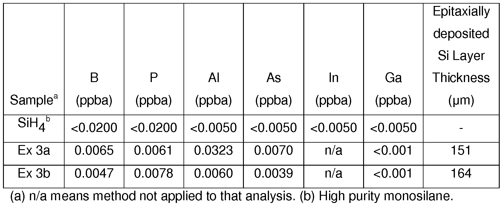
[0053] In Table 3, data for Ex 3a-3b reveal that while etching with H2(g) at Te 1240 °C for
60 minutes was sufficient to completely remove surface contaminants except Al (Ex 3a) from Intrinsic Substrate that was supported on a coated susceptor having only 1 Si coating layer to cap SiC layer, and therefore at least two Si coating layers to cap the SiC are preferred to consistently prevent migration of some contaminants (e.g., Al) into epitaxially deposited Si layer.
[0054] Ex 4: coated susceptor having 3 in situ Si coating layers. Loaded a SiC coated graphite susceptor into the reactor. Replicated Ar purge, vacuum evacuation, and H2 gas backfill of Ex 2a-2g. Then heated the susceptor to Te 1270 °C under H2 flow, and held etching for 30 minutes to etch the SiC coating of the susceptor. Ramped temperature down to T^ 1 150 °C and decreased H2 flow 5 L/min and stabilized. While holding T^ and H2 flow steady, injected high purity monosilane into the reactor at flow rate 7.5 cc/min. Grew a first inner Si coating layer slowly at low monosilane concentration and low H2 gas flow to obtain a dense and defect free Si layer. After 15 minutes deposition, the first inner Si coating layer was formed. Stopped the monosilane flow; and cooled the susceptor to < 600 °C under H2.
Heated the susceptor to Te 1 150 °C under H2(g) flow to etch the first inner Si coating layer surface. After 20 min H2 etching, the second inner Si coating layer was formed on the etched first inner Si coating layer. Repeated cooling/etching/depositing cycle used to make first inner Si coating layer another time to form the outermost Si coating layer on an etched second inner Si coating layer. The resulting multi (3) Si coating layer susceptor was then cooled to ambient temperature and ready for substrate loading.
[0055] Ex 5a-5c: Replicated Ex 2g three times except used the 3 Si coating layer susceptor of Ex 4 instead of the single Si coating layer susceptor of the General System and Procedure. Report analysis results below in Table 4.
[0056] Table 4.

(a) n/a means method not applied to that analysis; Sb <0.001 ppba. (b) High purity monosilane.
[0057] In Table 4, data for Ex 5a-5c reveal etching with H2(g) at Te 1240 °C for 60 minutes was sufficient to completely remove surface contaminants from Intrinsic Substrate that was supported on a coated susceptor having 3 Si coating layers to cap the SiC layer. The SiC susceptor contaminants did not confound the PL spectroscopy indirect adulterant analysis of the monosilane gas. The 3-layer Si coatings in Ex. 5a to 5c were better than the 1 -layer Si coating in Ex. 3a and 3b at preventing contamination of the epitaxially deposited silicon layer.
[0058] "May" confers a choice, not an imperative. Optionally" means is absent, alternatively is present. E.g., optionally one or more means 0, alternatively one or more. "Contact" comprises effective touching, e.g., as for facilitating reaction or deposition. Any reference herein to a Group or Groups of elements or the Periodic Table of the Elements means those of the 201 1 edition of the Periodic Table of the Elements promulgated by lUPAC (International Union of Pure and Applied Chemistry). All "%" and parts are, unless
otherwise noted, based on a total of 100% and total number of parts (e.g., 1 billion parts for ppba) and cover a range from 0 to 100% or 0 parts to relevant total number of parts unless otherwise indicated.
Claims
1 . A method of indirectly quantitatively characterizing at least one adulterant of a silane, the method comprising etching a contaminated surface of an otherwise high purity silicon substrate with an etching atmosphere consisting essentially of an etching gas under conditions effective for removing contaminants from the surface, thereby producing an ultraclean surface of the silicon substrate wherein the ultraclean surface is characterizable by a profile comprising: B < 0.030 parts per billion atomic (ppba); P < 0.030 ppba; Sb < 0.010 ppba; Ga < 0.010 ppba; In < 0.010 ppba; As < 0.010 ppba; Al < 0.033 ppba; and C < 200 ppba; epitaxially depositing silicon, made in situ from the silane, onto the ultraclean surface of the silicon substrate to give an epitaxially deposited silicon layer thereon; and analyzing the epitaxially deposited silicon layer so as to quantitatively characterize at least one deposited non-silicon element therein as a chemical element of the at least one adulterant.
2. The method of claim 1 , wherein the silane is quantitatively characterizable by the method as being high purity such that the epitaxially deposited silicon layer is characterizable by a profile comprising: B < 0.030 parts per billion atomic (ppba); P < 0.030 ppba; Sb < 0.010 ppba; Ga < 0.010 ppba; In < 0.010 ppba; As < 0.010 ppba; Al < 0.030 ppba; C < 200 ppba; or a combination of any two or more of B < 0.030 ppba; P < 0.030 ppba; Sb < 0.010 ppba; Ga < 0.010 ppba; In < 0.010 ppba; As < 0.010 ppba; Al < 0.030 ppba; and C < 200 ppba.
3. The method of claim 1 or 2, wherein the substrate is disposed within a reactor during the etching and depositing steps, and the reactor has inner surfaces exposed to the etching atmosphere and the etching further comprises etching the exposed surfaces in the reactor with the etching atmosphere so as to remove contaminants therefrom before the depositing step.
4. The method of any one of the preceding claims, wherein the etching atmosphere consists essentially of hydrogen gas, consists of hydrogen gas, or consists of hydrogen gas and at least one inert gas or vapor.
5. The method of any one of claims 1 to 3, wherein the etching atmosphere consists essentially of a halogen-based gas, consists of a halogen-based gas, or consists of a halogen-based gas and at least one inert gas or vapor, or consists of a mixture of hydrogen gas and a halogen-based gas, or consists of a mixture of hydrogen gas, a halogen-based gas, and an inert gas. The method of any one of claims 1 to 3, wherein the etching atmosphere consists essentially of a halogen-based gas or a mixture of hydrogen gas and a halogen- based gas, followed by hydrogen gas or a mixture of hydrogen gas and at least one inert gas or vapor.
The method of any one of the preceding claims, wherein the analyzing step comprises analyzing any carbon in the epitaxially deposited silicon layer by Secondary Ion Mass Spectrometry or Fourier Transform-Infrared spectroscopy, analyzing at least one non-silicon chemical element in the epitaxially deposited silicon layer by photoluminescence spectroscopy or Inductively Coupled Plasma- Mass Spectroscopy, or any combination of two or more thereof.
The method of any one of the preceding claims, wherein during the etching and depositing steps the substrate is supported on a coated susceptor comprising an inducible body, which is sequentially coated with a first Si coating layer, and an outermost Si coating layer, and optionally one or more interior Si coating layers sequentially disposed between the first and outermost Si coating layers.
A coated susceptor comprising an inducible body, which is sequentially coated with a first Si coating layer, and an outermost Si coating layer, and optionally one or more interior Si coating layers disposed between the first and outermost Si coating layers.
Applications Claiming Priority (2)
| Application Number | Priority Date | Filing Date | Title |
|---|---|---|---|
| US201261611055P | 2012-03-15 | 2012-03-15 | |
| US61/611,055 | 2012-03-15 |
Publications (2)
| Publication Number | Publication Date |
|---|---|
| WO2013138016A2 true WO2013138016A2 (en) | 2013-09-19 |
| WO2013138016A3 WO2013138016A3 (en) | 2013-12-05 |
Family
ID=47755057
Family Applications (1)
| Application Number | Title | Priority Date | Filing Date |
|---|---|---|---|
| PCT/US2013/026336 Ceased WO2013138016A2 (en) | 2012-03-15 | 2013-02-15 | Method of quantitatively characterizing adulterants of silanes and coated susceptor |
Country Status (2)
| Country | Link |
|---|---|
| TW (1) | TW201347032A (en) |
| WO (1) | WO2013138016A2 (en) |
Family Cites Families (2)
| Publication number | Priority date | Publication date | Assignee | Title |
|---|---|---|---|---|
| DE102010002342A1 (en) * | 2010-02-25 | 2011-08-25 | Evonik Degussa GmbH, 45128 | Use of the specific resistance measurement for indirect determination of the purity of silanes and germanes and a corresponding method |
| JP5668339B2 (en) * | 2010-06-30 | 2015-02-12 | 住友電気工業株式会社 | Manufacturing method of semiconductor device |
-
2013
- 2013-02-15 WO PCT/US2013/026336 patent/WO2013138016A2/en not_active Ceased
- 2013-02-21 TW TW102105969A patent/TW201347032A/en unknown
Non-Patent Citations (1)
| Title |
|---|
| None |
Also Published As
| Publication number | Publication date |
|---|---|
| WO2013138016A3 (en) | 2013-12-05 |
| TW201347032A (en) | 2013-11-16 |
Similar Documents
| Publication | Publication Date | Title |
|---|---|---|
| US7329593B2 (en) | Germanium deposition | |
| EP3879011A1 (en) | Sic semiconductor substrate, method for manufacturing same, and device for manufacturing same | |
| KR101339047B1 (en) | Method for producing polycrystalline silicon rods | |
| TWI541375B (en) | Formed sic product and method for producing the same | |
| CN104620355B (en) | The pollution quantity measuring method of epitaxially growing equipment and the manufacture method of epitaxial wafer | |
| US8343854B2 (en) | Method of reducing memory effects in semiconductor epitaxy | |
| KR100777321B1 (en) | In situ growth of oxide and silicon layers | |
| JP2017523950A5 (en) | ||
| WO2002097864A2 (en) | Low temperature load and bake | |
| US12237377B2 (en) | SiC semiconductor substrate, and, production method therefor and production device therefor | |
| JP2011233583A (en) | Vapor-phase growth device and method of manufacturing silicon epitaxial wafer | |
| CN103603048A (en) | Chemical vapor deposition equipment used for producing silicon carbide epitaxial wafer | |
| CN104878445A (en) | Preparation method of low-dosage concentration silicon carbide epitaxial material | |
| US20150311069A1 (en) | Method for manufacturing silicon carbide semiconductor substrate | |
| CN115747756B (en) | Epitaxial growth equipment restart method | |
| Tin et al. | CVD of SiC Epilayers–Basic Principles and Techniques | |
| TW201347032A (en) | Method for quantifying dopants of decane and coated heat exchanger | |
| CN114561705A (en) | Method for producing SiC wafer with residual stress control |
Legal Events
| Date | Code | Title | Description |
|---|---|---|---|
| 121 | Ep: the epo has been informed by wipo that ep was designated in this application |
Ref document number: 13706881 Country of ref document: EP Kind code of ref document: A2 |
|
| 122 | Ep: pct application non-entry in european phase |
Ref document number: 13706881 Country of ref document: EP Kind code of ref document: A2 |