WO2013122253A1 - Optical component, spectacle lens, and manufacturing methods therefor - Google Patents
Optical component, spectacle lens, and manufacturing methods therefor Download PDFInfo
- Publication number
- WO2013122253A1 WO2013122253A1 PCT/JP2013/053876 JP2013053876W WO2013122253A1 WO 2013122253 A1 WO2013122253 A1 WO 2013122253A1 JP 2013053876 W JP2013053876 W JP 2013053876W WO 2013122253 A1 WO2013122253 A1 WO 2013122253A1
- Authority
- WO
- WIPO (PCT)
- Prior art keywords
- multilayer film
- refractive index
- layer
- plastic substrate
- optical component
- Prior art date
Links
Images


Classifications
-
- G—PHYSICS
- G02—OPTICS
- G02B—OPTICAL ELEMENTS, SYSTEMS OR APPARATUS
- G02B1/00—Optical elements characterised by the material of which they are made; Optical coatings for optical elements
- G02B1/10—Optical coatings produced by application to, or surface treatment of, optical elements
- G02B1/11—Anti-reflection coatings
-
- G—PHYSICS
- G02—OPTICS
- G02C—SPECTACLES; SUNGLASSES OR GOGGLES INSOFAR AS THEY HAVE THE SAME FEATURES AS SPECTACLES; CONTACT LENSES
- G02C7/00—Optical parts
- G02C7/02—Lenses; Lens systems ; Methods of designing lenses
-
- C—CHEMISTRY; METALLURGY
- C23—COATING METALLIC MATERIAL; COATING MATERIAL WITH METALLIC MATERIAL; CHEMICAL SURFACE TREATMENT; DIFFUSION TREATMENT OF METALLIC MATERIAL; COATING BY VACUUM EVAPORATION, BY SPUTTERING, BY ION IMPLANTATION OR BY CHEMICAL VAPOUR DEPOSITION, IN GENERAL; INHIBITING CORROSION OF METALLIC MATERIAL OR INCRUSTATION IN GENERAL
- C23C—COATING METALLIC MATERIAL; COATING MATERIAL WITH METALLIC MATERIAL; SURFACE TREATMENT OF METALLIC MATERIAL BY DIFFUSION INTO THE SURFACE, BY CHEMICAL CONVERSION OR SUBSTITUTION; COATING BY VACUUM EVAPORATION, BY SPUTTERING, BY ION IMPLANTATION OR BY CHEMICAL VAPOUR DEPOSITION, IN GENERAL
- C23C14/00—Coating by vacuum evaporation, by sputtering or by ion implantation of the coating forming material
- C23C14/06—Coating by vacuum evaporation, by sputtering or by ion implantation of the coating forming material characterised by the coating material
- C23C14/08—Oxides
- C23C14/083—Oxides of refractory metals or yttrium
-
- C—CHEMISTRY; METALLURGY
- C23—COATING METALLIC MATERIAL; COATING MATERIAL WITH METALLIC MATERIAL; CHEMICAL SURFACE TREATMENT; DIFFUSION TREATMENT OF METALLIC MATERIAL; COATING BY VACUUM EVAPORATION, BY SPUTTERING, BY ION IMPLANTATION OR BY CHEMICAL VAPOUR DEPOSITION, IN GENERAL; INHIBITING CORROSION OF METALLIC MATERIAL OR INCRUSTATION IN GENERAL
- C23C—COATING METALLIC MATERIAL; COATING MATERIAL WITH METALLIC MATERIAL; SURFACE TREATMENT OF METALLIC MATERIAL BY DIFFUSION INTO THE SURFACE, BY CHEMICAL CONVERSION OR SUBSTITUTION; COATING BY VACUUM EVAPORATION, BY SPUTTERING, BY ION IMPLANTATION OR BY CHEMICAL VAPOUR DEPOSITION, IN GENERAL
- C23C14/00—Coating by vacuum evaporation, by sputtering or by ion implantation of the coating forming material
- C23C14/06—Coating by vacuum evaporation, by sputtering or by ion implantation of the coating forming material characterised by the coating material
- C23C14/10—Glass or silica
-
- C—CHEMISTRY; METALLURGY
- C23—COATING METALLIC MATERIAL; COATING MATERIAL WITH METALLIC MATERIAL; CHEMICAL SURFACE TREATMENT; DIFFUSION TREATMENT OF METALLIC MATERIAL; COATING BY VACUUM EVAPORATION, BY SPUTTERING, BY ION IMPLANTATION OR BY CHEMICAL VAPOUR DEPOSITION, IN GENERAL; INHIBITING CORROSION OF METALLIC MATERIAL OR INCRUSTATION IN GENERAL
- C23C—COATING METALLIC MATERIAL; COATING MATERIAL WITH METALLIC MATERIAL; SURFACE TREATMENT OF METALLIC MATERIAL BY DIFFUSION INTO THE SURFACE, BY CHEMICAL CONVERSION OR SUBSTITUTION; COATING BY VACUUM EVAPORATION, BY SPUTTERING, BY ION IMPLANTATION OR BY CHEMICAL VAPOUR DEPOSITION, IN GENERAL
- C23C14/00—Coating by vacuum evaporation, by sputtering or by ion implantation of the coating forming material
- C23C14/22—Coating by vacuum evaporation, by sputtering or by ion implantation of the coating forming material characterised by the process of coating
- C23C14/34—Sputtering
- C23C14/3464—Sputtering using more than one target
-
- C—CHEMISTRY; METALLURGY
- C23—COATING METALLIC MATERIAL; COATING MATERIAL WITH METALLIC MATERIAL; CHEMICAL SURFACE TREATMENT; DIFFUSION TREATMENT OF METALLIC MATERIAL; COATING BY VACUUM EVAPORATION, BY SPUTTERING, BY ION IMPLANTATION OR BY CHEMICAL VAPOUR DEPOSITION, IN GENERAL; INHIBITING CORROSION OF METALLIC MATERIAL OR INCRUSTATION IN GENERAL
- C23C—COATING METALLIC MATERIAL; COATING MATERIAL WITH METALLIC MATERIAL; SURFACE TREATMENT OF METALLIC MATERIAL BY DIFFUSION INTO THE SURFACE, BY CHEMICAL CONVERSION OR SUBSTITUTION; COATING BY VACUUM EVAPORATION, BY SPUTTERING, BY ION IMPLANTATION OR BY CHEMICAL VAPOUR DEPOSITION, IN GENERAL
- C23C14/00—Coating by vacuum evaporation, by sputtering or by ion implantation of the coating forming material
- C23C14/22—Coating by vacuum evaporation, by sputtering or by ion implantation of the coating forming material characterised by the process of coating
- C23C14/34—Sputtering
- C23C14/3471—Introduction of auxiliary energy into the plasma
-
- G—PHYSICS
- G02—OPTICS
- G02B—OPTICAL ELEMENTS, SYSTEMS OR APPARATUS
- G02B1/00—Optical elements characterised by the material of which they are made; Optical coatings for optical elements
- G02B1/04—Optical elements characterised by the material of which they are made; Optical coatings for optical elements made of organic materials, e.g. plastics
-
- G—PHYSICS
- G02—OPTICS
- G02B—OPTICAL ELEMENTS, SYSTEMS OR APPARATUS
- G02B1/00—Optical elements characterised by the material of which they are made; Optical coatings for optical elements
- G02B1/10—Optical coatings produced by application to, or surface treatment of, optical elements
- G02B1/11—Anti-reflection coatings
- G02B1/113—Anti-reflection coatings using inorganic layer materials only
- G02B1/115—Multilayers
-
- G—PHYSICS
- G02—OPTICS
- G02B—OPTICAL ELEMENTS, SYSTEMS OR APPARATUS
- G02B1/00—Optical elements characterised by the material of which they are made; Optical coatings for optical elements
- G02B1/10—Optical coatings produced by application to, or surface treatment of, optical elements
- G02B1/18—Coatings for keeping optical surfaces clean, e.g. hydrophobic or photo-catalytic films
-
- G—PHYSICS
- G02—OPTICS
- G02B—OPTICAL ELEMENTS, SYSTEMS OR APPARATUS
- G02B27/00—Optical systems or apparatus not provided for by any of the groups G02B1/00 - G02B26/00, G02B30/00
- G02B27/0006—Optical systems or apparatus not provided for by any of the groups G02B1/00 - G02B26/00, G02B30/00 with means to keep optical surfaces clean, e.g. by preventing or removing dirt, stains, contamination, condensation
-
- G—PHYSICS
- G02—OPTICS
- G02F—OPTICAL DEVICES OR ARRANGEMENTS FOR THE CONTROL OF LIGHT BY MODIFICATION OF THE OPTICAL PROPERTIES OF THE MEDIA OF THE ELEMENTS INVOLVED THEREIN; NON-LINEAR OPTICS; FREQUENCY-CHANGING OF LIGHT; OPTICAL LOGIC ELEMENTS; OPTICAL ANALOGUE/DIGITAL CONVERTERS
- G02F1/00—Devices or arrangements for the control of the intensity, colour, phase, polarisation or direction of light arriving from an independent light source, e.g. switching, gating or modulating; Non-linear optics
- G02F1/01—Devices or arrangements for the control of the intensity, colour, phase, polarisation or direction of light arriving from an independent light source, e.g. switching, gating or modulating; Non-linear optics for the control of the intensity, phase, polarisation or colour
- G02F1/13—Devices or arrangements for the control of the intensity, colour, phase, polarisation or direction of light arriving from an independent light source, e.g. switching, gating or modulating; Non-linear optics for the control of the intensity, phase, polarisation or colour based on liquid crystals, e.g. single liquid crystal display cells
- G02F1/133—Constructional arrangements; Operation of liquid crystal cells; Circuit arrangements
- G02F1/1333—Constructional arrangements; Manufacturing methods
- G02F1/1335—Structural association of cells with optical devices, e.g. polarisers or reflectors
- G02F1/133502—Antiglare, refractive index matching layers
Definitions
- the present invention relates to an optical component, a spectacle lens, and a manufacturing method thereof.
- This application claims priority based on Japanese Patent Application No. 2012-33167 for which it applied on February 17, 2012, and uses the content here.
- plastic lenses are frequently used as spectacle lenses because of their advantages of being lightweight, excellent in impact resistance and easy to dye.
- a plastic lens used for a spectacle lens is usually provided with an antireflection film on both sides.
- the antireflection film for spectacle lenses generally has low reflection characteristics (broadband low reflection characteristics) over the entire visible region of 400 nm to 700 nm.
- optical parts such as eyeglass lenses
- optical parts including a plastic base as disclosed in Patent Documents 1 to 3, and an antireflection film disposed on the base.
- LED liquid crystal screens and LED lighting which are the mainstream of displays, emit a lot of light in the vicinity of 450 nm, and thus control of light in such a blue region is attracting attention.
- dyeing lenses such as sunglasses are known.
- the dyed lens cuts the entire visible region, the visibility may deteriorate due to a decrease in the amount of light.
- the lens has a reflectance sufficient to obtain a sufficient effect, it feels troublesome due to the reflected light from the lens surface when worn as a spectacle lens.
- the curvature of the surface on which the light is incident is smaller than the curvature of the rear surface from which the light on the face side when worn out. For this reason, the light incident from the rear at the time of wearing is reflected on the surface and converges near the eyeball.
- reflection images such as room lights on the surface are conspicuous, and the appearance may be uncomfortable when viewed from a third party. In this way, when cutting a specific wavelength, it is necessary to select an appropriate surface to which the multilayer film is added and the reflectance.
- An aspect of the present invention provides an optical component, a spectacle lens, and a method for manufacturing the same having a filter function such as an antiglare effect, being effective in reducing fatigue, preventing eye diseases, and having good visibility. With the goal.
- An optical component according to an aspect of the present invention is an optical component that includes a plastic substrate and a multilayer film disposed on at least one of the surface and the rear surface of the plastic substrate that has a larger curvature.
- the multilayer film is characterized in that the maximum reflectance in the wavelength range of 380 to 780 nm is 3 to 50%.
- a method for manufacturing an optical component according to an aspect of the present invention includes a plastic base material, and a multilayer film disposed on at least a surface having a larger curvature among the surface and the rear surface of the plastic base material.
- a method of manufacturing an optical component comprising: heating the plastic substrate; and adjusting the plastic substrate to a predetermined temperature by the heating, and then forming the multilayer film on the plastic substrate.
- the step of forming the multilayer film includes a process of alternately stacking a plurality of high refractive index materials and low refractive index materials to form a high refractive index layer having a multilayer structure, and forming the high refractive index layer on the high refractive index layer.
- a low refractive index layer made of a low refractive index material having a lower refractive index than the refractive index layer, and setting the maximum reflectance in the wavelength range of 380 to 780 nm of the multilayer film to 3 to 50% Features To.
- the spectacle lens according to one embodiment of the present invention is a plastic base material having a front surface and a rear surface, and a first multilayer film provided on the surface, and has an average reflectance of 3 in a wavelength range of 380 nm to 780 nm. % Of the first multilayer film and the second multilayer film provided on the rear surface, and a wavelength range of 415 nm or more and 780 nm or less and a range of 30 nm including the first wavelength of the maximum reflectance.
- the second multilayer film having an average reflectance of 2% or more and 13% or less.
- the spectacle lens according to one embodiment of the present invention is a plastic base material having a front surface and a rear surface, and a first multilayer film provided on the surface, and has an average reflectance of 3 in a wavelength range of 380 nm to 780 nm. % Of the first multilayer film and the second multilayer film provided on the rear surface, and a range of 30 nm including the first wavelength in which the reflectance is maximum in the wavelength range of 380 nm or more and 500 nm or less.
- the second multilayer film having an average reflectance of 3% or more and 30% or less.
- the method for manufacturing a spectacle lens includes a step of heating a plastic substrate and a step of forming a multilayer film on the heated plastic substrate.
- the first multilayer film has an average reflectance of less than 3% in a wavelength range of 380 nm or more and 780 nm or less
- the second multilayer film provided on the rear surface has a reflectance in a wavelength range of 380 nm or more and 500 nm or less.
- a sufficient filter function such as an antiglare effect can be obtained while maintaining good visibility.
- the method for manufacturing an optical component according to one embodiment of the present invention it is possible to provide an optical component that has reduced optical dazzling, is easily visible, and has optical characteristics that are effective for fatigue and prevention of eye diseases. Become.
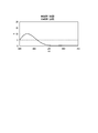
- FIG. 6 is a spectral characteristic diagram of a multilayer film on the rear surface of the lens of Example 1 and the surface of the lens of Comparative Example 1.
- FIG. 6 It is the spectral characteristic data of the multilayer film concerning the back surface of the lens of Example 1, and the surface of the lens of the comparative example 1.
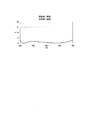
- 6 is a spectral characteristic diagram of a multilayer film on the surface of the lens of Example 1 and the rear surface of the lens of Comparative Example 1.
- FIG. It is the spectral characteristic data of the multilayer film concerning the surface of the lens of Example 1, and the rear surface of the lens of Comparative Example 1.
- 6 is a spectral characteristic diagram of a multilayer film on the rear surface of the lens of Example 2 and the surface of the lens of Comparative Example 2.
- FIG. It is the spectral characteristic data of the multilayer film concerning the rear surface of the lens of Example 2, and the surface of the lens of Comparative Example 2.
- 6 is a spectral characteristic diagram of a multilayer film on the surface of the lens of Example 2 and the rear surface of the lens of Comparative Example 2.
- FIG. 6 is a spectral characteristic diagram of a multilayer film on the rear surface of the lens of Example 3 and the surface of the lens of Comparative Example 3.
- FIG. 6 It is the spectral characteristic data of the multilayer film concerning the back surface of the lens of Example 3, and the surface of the lens of the comparative example 3.
- FIG. 6 is a spectral characteristic diagram of a multilayer film on the surface of the lens of Example 3 and the rear surface of the lens of Comparative Example 3.
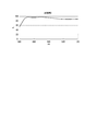
- 6 is a transmission characteristic diagram of the lens of Example 1.
- FIG. It is the transmission characteristic data of the lens of Example 1.
- 6 is a transmission characteristic diagram of the lens of Example 2.
- FIG. It is the transmission characteristic data of the lens of Example 2.
- 6 is a transmission characteristic diagram of the lens of Example 3.
- FIG. 11 is a spectral characteristic diagram of a multilayer film applied to the rear surface of the lens of Example 4 and the surface of the lens of Example 5. It is the spectral characteristic data of the multilayer film concerning the back surface of the lens of Example 4, and the surface of the lens of Example 5.
- FIG. FIG. 12 is a spectral characteristic diagram of a multilayer film on the surface of the lens of Example 4 and the rear surface of the lens of Example 5.
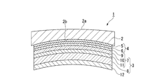
- FIG. 1 is a side sectional view schematically showing a first embodiment of the optical component of the present invention.
- reference numeral 1 denotes an optical component for a spectacle lens.
- the optical component 1 includes a plastic substrate 2 and an inorganic multilayer film 3 disposed on the surface of the plastic substrate 2 having the larger curvature.
- the rear surface 2b is the surface with the larger curvature.
- a functional thin film 4 is disposed between the rear surface 2 b of the plastic substrate 2 and the inorganic multilayer film 3.
- the functional thin film 4 includes a primer layer 5 and a hard coat layer 6 in this embodiment.
- an arbitrary film corresponding to the inorganic multilayer film 3 and the functional thin film 4 is also formed on the surface 2a (the surface with the smaller curvature) of the plastic substrate 2, but this film is illustrated. The description is omitted.
- the plastic substrate 2 is, for example, a transparent plastic such as acrylic resin, thiourethane resin, methacrylic resin, allyl resin, episulfide resin, polycarbonate resin, polyurethane resin, polyester resin, polystyrene resin, episulfide. Resin, polyethersulfone resin, poly-4-methylpentene-1 resin, diethylene glycol bisallyl carbonate resin (CR-39), polyvinyl chloride resin, halogen-containing copolymer, sulfur-containing copolymer, etc. It is.
- the refractive index (nd) of the plastic substrate 2 is selected from, for example, 1.50, 1.60, 1.67, and 1.74.
- the plastic base material 2 when making the refractive index of the plastic base material 2 1.6 or more, as the plastic base material 2, an allyl carbonate resin, an acrylate resin, a methacrylate resin, a thiourethane resin, or the like can be used. .
- the frequency of the plastic substrate 2 can be a negative value.
- the curvature of the back surface in such a base material is larger than the curvature of the surface.
- the plastic substrate 2 may not be transparent as long as it has translucency, and may be colored.
- the transmittance of the colored plastic substrate 2 can be 5 to 85%.
- the functional thin film 4 is disposed between the plastic substrate 2 and the inorganic multilayer film 3 as described above, and is in contact with the primer layer 5 disposed in contact with the plastic substrate 2, and And a hard coat layer 6 disposed in contact with the inorganic multilayer film 3.
- the primer layer 5 is for improving the adhesion between the plastic substrate 2 and the hard coat layer 6 and functions as an adhesion layer. Moreover, it is also for absorbing the impact on the optical component 1 and functions as an impact absorbing layer.
- the primer layer 5 is mainly composed of a polyurethane-based resin.
- the primer layer 5 is a polyurethane-based resin containing, for example, fine particles of an inorganic material.
- the primer layer 5 may include at least one of acrylic resin, methacrylic resin, and organosilicon resin.
- the thickness (actual thickness) of the primer layer 5 can be about 0.5 ⁇ m or more and 1.0 ⁇ m or less.
- the primer layer 5 can be formed on the plastic substrate 2 with a predetermined thickness by immersing the plastic substrate 2 in the forming material solution of the primer layer 5 and then lifting and drying.
- a material for forming the primer layer 5 for example, a solution obtained by dispersing or dissolving the resin to be the primer layer 5 and the inorganic oxide fine particle sol in water or an alcohol solvent and mixing them can be used.
- the hard coat layer 6 has a function of protecting the plastic substrate 2 and suppressing damage to the plastic substrate 2, and functions as a scratch-resistant film.
- the hard coat layer 6 is made of, for example, an organosiloxane hard coat layer.
- the organosiloxane hard coat layer is obtained by dispersing inorganic oxide fine particles in an organosiloxane resin.
- the inorganic oxide for example, rutile-type titanium oxide, and oxides of silicon, tin, zirconium, and antimony are used.
- the hard coat layer 6 may be an organosilicon resin containing colloidal silica as disclosed in, for example, Japanese Patent Publication No. 4-55615.
- the thickness (actual thickness) of the hard coat layer 6 can be about 2 ⁇ m or more and 4 ⁇ m or less.
- the hard coat layer 6 is formed on the primer layer 5 on the plastic substrate 2 by immersing the plastic substrate 2 on which the primer layer 5 is formed in the forming material solution of the hard coat layer 6, and then pulling up and drying. It can be formed with a thickness of As a forming material liquid for the hard coat layer 6, for example, a liquid obtained by dispersing or dissolving the resin to be the hard coat layer 6 and the inorganic oxide fine particle sol in water or an alcohol solvent and mixing them can be used. .
- the functional thin film 4 and the plastic substrate can be used as long as the refractive index of the functional thin film 4 and the refractive index of the plastic substrate 2 are substantially the same. Generation of interference fringes caused by reflection at the interface with the material 2 and a decrease in transmittance can be suppressed. Therefore, the refractive index of the functional thin film 4 is adjusted according to the refractive index of the plastic substrate 2.
- the refractive index of the functional thin film 4 (primer layer 5 and hard coat layer 6) can be adjusted by selecting the type (physical properties) of the resin that is the main component of the functional thin film 4, or for the resin that is the main component. This can be done by selecting the type (physical properties) of the fine particles to be added.
- the functional thin film 4 is formed including the primer layer 5 and the hard coat layer 6.
- the primer layer 5 and the hard coat layer 6 are formed. It may be omitted.
- a dielectric film or a metal film made of ITO (Indium Tin Oxide) or the like may be provided in addition to the primer layer 5 and the hard coat layer 6.
- a dielectric film or a metal film having a thickness of 20 nm or less may be disposed between the high refractive index inorganic material and the low refractive index inorganic material constituting the inorganic multilayer film. Note that the thickness of the dielectric film or the metal film may be 10 nm or less.
- the inorganic multilayer film 3 has a high refractive index layer 7 having a multilayer structure in which a plurality of high refractive index inorganic materials and low refractive index inorganic materials are alternately laminated on the plastic substrate 2. On top of this, a multi-layer having a low refractive index layer 8 made of a low refractive index inorganic material having a lower refractive index than the high refractive index layer 7 is formed.
- the inorganic multilayer film 3 is designed so that the maximum reflectance in the wavelength range of 380 to 780 nm is 3 to 50%.
- the maximum reflectance when used as a spectacle lens, a filter function such as a sufficient antiglare effect can be obtained and good visibility can be maintained.
- the maximum reflectance in this wavelength range is set to less than 3%, those who wear such glasses may not be able to expect sufficient filter functions such as anti-glare effect, fatigue prevention effect, and eye disease prevention effect.
- the reflectance maximum value in this wavelength region is set to exceed 50%, the amount of transmitted light may decrease and visibility may deteriorate.
- the maximum reflectance can be 3 to 35%, and preferably 3 to 15%.
- an inorganic multilayer film is used as the multilayer film, but an organic multilayer film may be used as long as the effects of the present invention are not impaired.
- an antireflection film having an average reflectance of 5.0% or less in the wavelength region of 380 to 780 nm can be disposed on the surface 2a (the surface with the smaller curvature).
- the average reflectance of the antireflection film is preferably 3.5% or less, and preferably 2.0% or less from the viewpoint of obtaining better visibility.
- the high refractive index layer 7 includes a first layer 9 made of a high refractive index inorganic material provided on the plastic substrate 2 side, and a low refractive index inorganic material provided on the first layer 9. And a third layer 11 made of a high refractive index inorganic material provided on the second layer 10.
- the first layer 9 is provided in contact with the hard coat layer 6 and is made of zirconium dioxide (ZrO 2 ) having a refractive index of 2.0.
- ZrO 2 zirconium dioxide
- titanium dioxide (TiO 2 ) or tantalum dioxide (Ta 2 O 5 ) can be used as the high refractive index inorganic material constituting the first layer 9.
- it can also be formed of an oxide of an alloy composed of a plurality of kinds of zirconium, titanium, and tantalum.
- Y 2 O 3 yttrium dioxide
- Nb 2 O 5 niobium dioxide
- the adhesion between the first layer 9 and the hard coat layer 6 can be improved by forming the first layer 9 with the high refractive index inorganic material (ZrO 2 ).
- the adhesion (adhesive strength) between the layer (ZrO 2 ) made of the high refractive index inorganic material and the hard coat layer 6 is more closely adhered to the layer (SiO 2 ) made of the low refractive index inorganic material and the hard coat layer 6. This is because it is larger than the property (adhesion).
- the adhesion (adhesion) between the high refractive index layer (ZrO 2 ) and the plastic substrate 2 is lower. Since it is larger than the adhesiveness (adhesive force) between the rate layer (SiO 2 ) and the plastic substrate 2, the adhesiveness becomes more advantageous.
- the second layer 10 is provided in contact with the first layer 9 and is made of silicon dioxide (SiO 2 ) having a refractive index of 1.47.
- SiO 2 silicon dioxide
- MgF 2 having a refractive index of 1.36 can be used as the low refractive index inorganic material constituting the second layer 10 in addition to SiO 2 .
- the third layer 11 is provided in contact with the second layer 10 and is made of zirconium dioxide (ZrO 2 ) in the same manner as the first layer 9.
- the third layer 11 can also be formed of a high refractive index inorganic material other than ZrO 2 , similarly to the first layer 9. Further, the high refractive index layer 7 is not formed in the three-layer structure of the first layer 9, the second layer 10, and the third layer 11 as described above. It can also be composed of layers, or four or more layers.
- the low refractive index layer 8 is provided in contact with the third layer 11 and is made of silicon dioxide (SiO 2 ) as in the second layer 10.
- the fluorine-containing alkyl group-containing organosilicon compound is included on the inorganic multilayer film 3, that is, on the outermost layer (low refractive index layer 8) of the inorganic multilayer film 3 farthest from the plastic substrate 2.
- a water / oil repellent film 12 is provided.
- the water / oil repellent film 12 is mainly composed of a fluorine-substituted alkyl group-containing organosilicon compound and has liquid repellency (water repellency, oil repellency). That is, this water / oil repellent film 12 reduces the surface energy of the optical component, exhibits functions of preventing water scorching and dirt, and improves the sliding performance of the surface of the optical component. As a result, scratch resistance is improved. Can be improved.
- the fluorine-substituted alkyl group-containing organosilicon compound the following general formula (1):
- Rf represents a linear or branched perfluoroalkyl group having 1 to 16 carbon atoms
- Y represents iodine or hydrogen
- Y ′ represents hydrogen or a lower alkyl group having 1 to 5 carbon atoms.
- Y ′′ represents a fluorine or trifluoromethyl group
- R 1 represents a hydrolyzable group
- R 2 represents hydrogen or an inert monovalent organic group
- a, b, c, d are Each represents an integer of 0 to 200, e represents 0 or 1, s and t each represents an integer of 0 to 2, and w represents an integer of 1 to 10)
- X represents oxygen or a divalent organic group
- X ′ represents a hydrolyzable group
- X ′′ represents a divalent organic silicone group
- R 3 represents carbon.
- q represents an integer of 1 to 3
- m, n and o each represents an integer of 0 to 200
- p represents 1 or 2
- r Represents an integer of 2 to 20
- k represents an integer of 0 to 2
- z represents an integer of 0 to 10 when k is 0 or 1
- Rf 2 represents a divalent linear perfluoropolyether group
- R 4 represents an alkyl group having 1 to 4 carbon atoms or a phenyl group
- R 5 represents a hydrolyzable group.
- I represents an integer of 0 to 2
- j represents an integer of 1 to 5
- u represents 2 or 3.
- a fluorine-substituted alkyl group-containing organosilicon compound selected from the general formulas (1) to (5) and the general formula (6) The selected fluorine-substituted alkyl group-containing organosilicon compound can be used in combination.
- the fluorine-substituted alkyl group-containing organosilicon compound represented by the general formulas (1) to (5) OPTOOL-DSX, OPTOOL-AES4, etc. manufactured by Daikin Industries, Ltd. can be used.
- As the fluorine-substituted alkyl group-containing organosilicon compound represented by the general formula (6) KY-130, KY-164 manufactured by Shin-Etsu Chemical Co., Ltd. can be used.
- FIG. 2 is a side sectional view schematically showing a second embodiment of the optical component of the present invention.
- reference numeral 1 ′ denotes an optical component for a spectacle lens.
- the optical component 1 ′ includes an inorganic multilayer film 3 ′ disposed on the surface 2a (the surface with the smaller curvature) of the plastic substrate 2.
- the rear surface 2b is the surface with the larger curvature.
- a functional thin film 4 is disposed between the surface 2a of the plastic substrate 2 and the inorganic multilayer film 3 ′. This functional thin film 4 is composed of a primer layer 5 and a hard coat layer 6 in this embodiment.
- the inorganic multilayer film 3 ′ has a high refractive index layer 7 ′ having a multilayer structure in which a plurality of high refractive index inorganic materials and low refractive index inorganic materials are alternately stacked on the plastic substrate 2.
- a multi-layer having a low refractive index layer 8 ′ made of a low refractive index inorganic material having a lower refractive index than the high refractive index layer 7 ′ is formed.
- the high refractive index layer 7 ′ includes a first layer 9 ′ made of a high refractive index inorganic material provided on the plastic substrate 2 side, and a low refractive index provided on the first layer 9 ′. It consists of a second layer 10 'made of an inorganic material and a third layer 11' made of a high refractive index inorganic material provided on the second layer 10 '. Inorganic materials used for the first layer 9 ′, the second layer 10 ′, and the third layer 11 ′ in the present embodiment include the first layer 9, the second layer 10, and the third layer 11 in the first embodiment. The thing similar to the inorganic material used is mentioned.
- the high refractive index layer 7 ′ can be composed of two layers or four or more layers without forming it in a three-layer structure like the high refractive index layer 7 in the first embodiment.
- the inorganic multilayer film 3 ′ disposed on the surface with the smaller curvature (surface 2a) has a maximum reflectance in the wavelength range of 380 to 780 nm and the surface with the larger curvature (rear surface 2b). ) It is designed to be smaller than the maximum reflectance of the inorganic multilayer film 3 disposed thereon. That is, the maximum reflectance of the inorganic multilayer film 3 disposed on the surface with the larger curvature (rear surface 2b) is the inorganic multilayer film 3 ′ disposed on the surface with the smaller curvature (surface 2a). Greater than the maximum reflectance.
- the inorganic multilayer film 3 disposed on the rear surface 2b of the plastic substrate 2 is designed such that the maximum reflectance is 4 to 35%, and is designed to be 4 to 15%. preferable.
- the inorganic multilayer film 3 ′ disposed on the surface 2a of the plastic substrate 2 is designed so that the maximum reflectance is 3 to 30%, and is preferably designed to be 3 to 10%. .
- the multilayer film 3 ′ (first multilayer film) provided on the surface 2 a can have an average reflectance of 3% or less in a wavelength range of 380 nm or more and within 780 nm, and the multilayer film 3 ( The second multilayer film) has an average reflectance of 2% or more and 13% in the range of 30 nm including the wavelength of the maximum reflectance (first wavelength) in the wavelength range of 415 nm or more and within 780 nm (or 750 nm).
- first wavelength the maximum reflectance
- the multilayer film 3 ′ (first multilayer film) provided on the surface 2 a can have an average reflectance of less than 3% in a wavelength range of 380 nm or more and within 780 nm, and the multilayer film 3 ( The second multilayer film) can have an average reflectance of 3% or more and 30% or less in a 30 nm range including a wavelength (first wavelength) having a maximum reflectance in a wavelength range of 380 nm or more and 500 nm or less.
- the multilayer film 3 ′ (first multilayer film) has an average reflectance of less than 1.5% in the wavelength range of 380 nm or more and 780 nm or less, and an average reflectance of 3% in the wavelength range of 380 nm or more and 500 nm or less. Can be less.
- the difference from the maximum reflectance can be 2 to 49%.
- the difference in the maximum reflectance is preferably 2 to 10%.
- the difference in the reflectance maximum value is preferable. Is preferably 2 to 15%, and when the radius of curvature of the surface is 1500 mm or more, the difference in maximum reflectance is preferably 5 to 15%.
- the difference from the reflectance of the (2 multilayer film) 3 can be 1% or more and within 10%.
- the difference from the reflectance of 3 can be 3% or more and 41% or less.
- the functional thin film 4 is formed including the primer layer 5 and the hard coat layer 6.
- the primer layer 5 and the hard coat layer 6 include Of these, either one or both may be omitted.
- a dielectric film or a metal film made of ITO (Indium Tin Oxide) or the like may be provided in addition to the primer layer 5 and the hard coat layer 6.
- a dielectric film or a metal film having a thickness of 20 nm or less may be disposed between the high refractive index inorganic material and the low refractive index inorganic material constituting the inorganic multilayer film. Note that the thickness of the dielectric film or the metal film may be 10 nm or less.
- an inorganic multilayer film is used as the multilayer film, but an organic multilayer film may be used as long as the effects of the present invention are not impaired.
- the optical component manufacturing method of the present embodiment includes a step of forming a functional thin film 4 (primer layer 5 and hard coat layer 6) on a plastic substrate 2 by a method similar to the conventional method, and heating the plastic substrate 2.
- a predetermined temperature for example, 70 ° C.
- the step of forming the inorganic multilayer film 3 includes a process of alternately stacking a plurality of high refractive index inorganic materials and low refractive index inorganic materials to form a high refractive index layer 7 having a multilayer structure, And forming a low refractive index layer 8 made of a low refractive index inorganic material.
- a vacuum deposition method is used to form each of these layers.
- FIG. 3 is a diagram illustrating an example of a vapor deposition apparatus 30 for forming each layer of the inorganic multilayer film 3.
- the vapor deposition apparatus 30 includes a first film formation chamber 31, a second film formation chamber 32, and a third film formation chamber 33.
- Each of the first film forming chamber 31, the second film forming chamber 32, and the third film forming chamber 33 is configured so that the inside of each of the first film forming chamber 31, the second film forming chamber 32, and the third film forming chamber 33 is maintained in that state.
- the vapor deposition apparatus 30 can adjust the internal temperature of each of the first film forming chamber 31, the second film forming chamber 32, and the third film forming chamber 33 by a temperature control unit (not shown).
- the vapor deposition apparatus 30 includes a holding member 34 in each internal space of the first film formation chamber 31, the second film formation chamber 32, and the third film formation chamber 33.
- the holding member 34 has a curved upper surface (holding surface) and is configured to be rotatable, and holds a plurality of plastic substrates 2 on the upper surface.
- the vapor deposition source 35 of the vapor deposition apparatus 30 is disposed in a space inside the second film formation chamber 32.
- the vapor deposition source 35 includes a first vapor deposition source 35A and a second vapor deposition source 35B.
- a light source device 36 capable of irradiating the vapor deposition source 35 with a beam is disposed.
- the light source device 36 can strike the constituent particles of the vapor deposition source 35 by irradiating the vapor deposition source 35 with electrons.
- a material (gas) for forming the inorganic multilayer film 3 is emitted from the vapor deposition source 35.
- the light source device 36 irradiates the first vapor deposition source 35A with a beam
- the vapor of ZrO 2 is discharged from the first vapor deposition source 35A, and is supplied onto the plastic substrate 2 held by the holding member 34 for vapor deposition.
- the first layer 9 and the third layer 11 in the high refractive index layer 7 of the inorganic multilayer film 3 can be formed.
- SiO 2 vapor is released from the second vapor deposition source 35B, and is supplied onto the plastic substrate 2 held by the holding member 34 for vapor deposition.
- the second layer 10 and the low refractive index layer 8 in the high refractive index layer 7 of the inorganic multilayer film 3 can be formed.
- the high refractive index inorganic material is formed on the plastic substrate 2 held by the holding member 34. And layers made of a low refractive index inorganic material can be alternately formed and laminated.
- the inorganic multilayer film 3 is designed so that the maximum reflectance in the wavelength range of 380 to 780 nm is 3 to 50%.
- the surface with the smaller curvature (surface 2a) is provided with an antireflection film, and this antireflection film is designed so that the reflectance is 5.0% or less in the wavelength region of 380 to 780 nm. .
- a vapor deposition source made of zirconium oxide (ZrO) is used as the first vapor deposition source 35A, and the first vapor deposition source 35A is irradiated with a beam while introducing oxygen into the internal space of the second chamber 32, so that zirconium dioxide (ZrO 2 ). You may make it form the high refractive index inorganic material layer which consists of these.
- the step of forming the inorganic multilayer film 3 includes the step of forming a film while performing ion beam assist on at least one of the layers constituting the inorganic multilayer film 3. May be included.
- a dielectric film is disposed between the high refractive index inorganic material and the low refractive index inorganic material constituting the inorganic multilayer film. .
- FIG. 4 is a diagram illustrating an example of a film forming apparatus 30 ′ for performing ion beam assist.
- the film forming apparatus 30 ′ includes an ion gun 37 in the second film forming chamber of the film forming apparatus 30 shown in FIG.
- the film is formed while performing ion beam assist. I do.
- At least one of the layers constituting the inorganic multilayer film 3 in the second film forming chamber 32 may be formed while performing ion beam assist, and the target to be subjected to ion beam assist is limited to the dielectric film. Not.
- the second film forming chamber 32 of the film forming apparatus 30 ′ includes a holding member 34 that holds the base material on which the high refractive index layer 7 is formed on the plastic base material 2, and an evaporation source 35 ′. And an ion gun 37 disposed apart from the vapor deposition source 35 ′ and a light source device 36. Further, the inside of the film forming apparatus 30 ′ is depressurized to a substantially vacuum, and the periphery of the plastic substrate 2 can be maintained in a vacuum atmosphere.
- an atmospheric gas supply source such as a gas cylinder is connected to the film forming apparatus 30 ′, and the inside of the vacuum vessel is in a low pressure state such as a vacuum, and an oxygen gas, argon gas, or other inert gas atmosphere, Alternatively, an inert gas atmosphere containing oxygen can be used.
- the vapor deposition source 35 includes, for example, ITO.
- ITO indium gallium trioxide
- the gasified ITO is emitted from the vapor deposition source 35 ′ and supplied to the plastic substrate 2 held by the holding member 34.
- a dielectric film made of ITO can be formed on the high refractive index layer 7.
- the ion gun apparatus includes an ion gun 37 disposed inside the second film forming chamber 32, a gas introduction unit (not shown) for introducing a gas to be ionized, and an extraction electrode (not shown) provided in front of the ion gun 37. .
- the ion gun apparatus ionizes a part of gas atoms or molecules, generates ion beams by controlling the ionized particles with an electric field generated by an extraction electrode, and irradiates a sample with the ion beams.
- the light source device 36 has the same configuration as the ion gun 37, and can irradiate the vapor deposition source 35 'with electrons to knock out the constituent particles of the vapor deposition source 35'.
- a voltage is applied to the vapor deposition source 35 ′ with a high-frequency coil or the like to form the constituent particles of the vapor deposition source 35 ′.
- the light source device 36 may be omitted.
- an ITO dielectric film is formed on the high refractive index layer 7 on the plastic substrate 2 using the film forming apparatus 30 ′ having the above-described configuration.
- an ITO vapor deposition source 35 ′ is used, and ions irradiated from the ion gun 37 can be irradiated onto the upper surface of the holding member 34.
- the inside of the film forming chamber 32 containing the plastic substrate 2 is evacuated to make a reduced pressure atmosphere. Then, the ion gun 37 and the light source device 36 are operated.
- the constituent particles of the vapor deposition source 35 ′ are knocked out and fly onto the high refractive index layer 7. Then, the constituent particles knocked out from the vapor deposition source 35 ′ are deposited on the high refractive index layer 7, and at the same time, argon ions are irradiated from the ion gun 37.
- ion beam assist is performed using at least one gas selected from an inert gas, an oxygen gas, and a mixed gas of an inert gas and an oxygen gas.
- This inert gas can be argon.
- a water / oil repellent film 12 is formed on the inorganic multilayer film 3.
- a wet method such as a dipping method, a spin coat method and a spray method, or a dry method such as a vacuum deposition method.
- the dipping method is common and is often used.
- This method is a method in which an optical component formed up to the inorganic multilayer film 3 is immersed in a solution in which a fluorine-substituted alkyl group-containing organosilicon compound is dissolved in an organic solvent, pulled up under certain conditions, and dried to form a film.
- the organic solvent perfluorohexane, perfluoro-4-methoxybutane, perfluoro-4-ethoxybutane, metaxylene hexafluoride or the like is used.
- the dilution concentration with the organic solvent can be 0.01 to 0.5% by weight, preferably 0.03 to 0.1% by weight. If the concentration is too low, the water / oil repellent layer 12 having a sufficient film thickness may not be obtained. If the concentration is too high, uneven coating tends to occur and the material cost may increase. Of the dry methods, vacuum deposition is often used. This method is a method of forming the water- and oil-repellent film 12 by heating and evaporating the fluorine-substituted alkyl group-containing organosilicon compound in a vacuum chamber.
- the inorganic multilayer film 3 disposed on at least one of the surface 2a and the rear surface 2b of the plastic substrate 2 having a larger curvature is formed at 380 to 780 nm. Since the maximum reflectance in the wavelength range of 3 to 50% is designed, good performance can be ensured for both the reflection characteristics and the visibility as described above. Moreover, in the manufacturing method of an optical component, such a well-balanced and excellent optical component can be reliably provided.
- a silicon hard coat having a refractive index of 1.67 and a primer coat having a refractive index of 1.67 were applied by heat curing on a urethane synthetic resin substrate, and a film was formed by vacuum deposition as described below.
- the frequency is in the range of -1.00D to -6.00D
- the radius of curvature of the surface is in the range of 200 mm to 1300 mm
- the radius of curvature of the rear surface is in the range of 100 mm to 170 mm.
- the one inside was used.
- the curvature radius of the rear surface of each substrate is smaller than the curvature radius of the surface, and the curvature of the rear surface is larger than the curvature of the surface.
- Rear side (face side): Set the lens in a rotating dome provided in the vacuum chamber, heat the temperature in the vacuum chamber to 70 degrees, and exhaust until the pressure becomes 1.0 ⁇ 10 ⁇ 3 Pa, After performing Ar ion beam cleaning for 60 seconds under conditions of an acceleration voltage of 500 V and an acceleration current of 100 mA, the first layer ZrO 2 (refractive index of 2.00) is sequentially applied from the plastic substrate side to an optical film thickness of 0.155 ⁇ , The second layer SiO 2 (refractive index 1.47) has an optical film thickness of 0.045 ⁇ , the third layer ZrO 2 (refractive index 2.00) has an optical film thickness of 0.485 ⁇ , and the fourth layer SiO 2 (refractive index 1).
- the first layer ZrO 2 (refractive index 2.00) has an optical film thickness of 0.035 ⁇
- the second layer SiO 2 (refractive The optical thickness is 0.135 ⁇
- the third layer ZrO 2 (refractive index 2.00) is optical thickness 0.04 ⁇
- the fourth layer SiO 2 (refractive index 1.47) is optical.
- the film thickness is 0.500 ⁇
- the fifth layer ZrO 2 (refractive index 2.00) has an optical film thickness of 0.150 ⁇
- the sixth layer SiO 2 (refractive index 1.47) has an optical film thickness of 0.06 ⁇ .
- the layer ZrO 2 (refractive index 2.00) was laminated with an optical film thickness of 0.225 ⁇
- the eighth layer SiO 2 (refractive index 1.47) was laminated with an optical film thickness of 0.280 ⁇ . Note that ⁇ is 485 nm as the center wavelength of the design.
- the first layer ZrO 2 (refractive index 2.00) has an optical film thickness of 0.155 ⁇ and the second layer SiO 2 (refractive The refractive index 1.47) is the optical film thickness 0.045 ⁇ , the third layer ZrO 2 (refractive index 2.00) is the optical film thickness 0.485 ⁇ , and the fourth layer SiO 2 (refractive index 1.47) is optical.
- the films were stacked with a film thickness of 0.335 ⁇ . Note that ⁇ is 500 nm as the design center wavelength.
- Spectral characteristic diagrams and spectral characteristic data on the rear surface of the lens of Example 1 and the surface of the lens of Comparative Example 1 are shown in FIGS. 5A and 5B, and the spectral characteristic diagrams on the surface of the lens of Example 1 and the rear surface of the lens of Comparative Example 1 are shown. The spectral characteristic data are shown in FIGS. 6A and 6B.
- the fifth layer ZrO 2 (refractive index 2.00) has an optical film thickness of 0.235 ⁇
- the sixth layer SiO 2 (refractive index 1.47) has an optical film thickness.
- Lamination was performed at 0.240 ⁇ . Note that ⁇ is 500 nm as the design center wavelength.
- the first layer ZrO 2 (refractive index 2.00) has an optical film thickness of 0.035 ⁇
- the second layer SiO 2 (refractive The optical thickness is 0.135 ⁇
- the third layer ZrO 2 (refractive index 2.00) is optical thickness 0.04 ⁇
- the fourth layer SiO 2 (refractive index 1.47) is optical.
- the film thickness is 0.500 ⁇
- the fifth layer ZrO 2 (refractive index 2.00) has an optical film thickness of 0.150 ⁇
- the sixth layer SiO 2 (refractive index 1.47) has an optical film thickness of 0.06 ⁇ .
- the layer ZrO 2 (refractive index 2.00) was laminated with an optical film thickness of 0.225 ⁇ , and the eighth layer SiO 2 (refractive index 1.47) was laminated with an optical film thickness of 0.280 ⁇ . Note that ⁇ is 485 nm as the center wavelength of the design.
- the first layer ZrO 2 (refractive index 2.00) has an optical film thickness of 0.10 ⁇
- the second layer SiO 2 (refractive The optical thickness is 0.505 ⁇
- the third layer ZrO 2 (refractive index 2.00) is optical thickness 0.215 ⁇
- the fourth layer SiO 2 (refractive index 1.47) is optical.
- a film thickness of 0.065 ⁇ , a fifth layer ZrO 2 (refractive index of 2.00) with an optical film thickness of 0.235 ⁇ , and a sixth layer of SiO 2 (refractive index of 1.47) with an optical film thickness of 0.240 ⁇ were laminated. .
- ⁇ is 500 nm as the design center wavelength.
- Spectral characteristic diagrams and spectral characteristic data on the rear surface of the lens of Example 2 and the surface of the lens of Comparative Example 2 are shown in FIGS. 7A and 7B, and the spectral characteristic diagrams on the surface of the lens of Example 2 and the rear surface of the lens of Comparative Example 2 are shown.
- the spectral characteristic data are shown in FIGS. 8A and 8B.
- Example 3 Rear side (face side): Set the lens in a rotating dome provided in the vacuum chamber, heat the temperature in the vacuum chamber to 70 degrees, and exhaust until the pressure becomes 1.0 ⁇ 10 ⁇ 3 Pa, After performing Ar ion beam cleaning for 60 seconds under conditions of an acceleration voltage of 500 V and an acceleration current of 100 mA, the first layer ZrO 2 (refractive index of 2.00) is sequentially applied from the plastic substrate side to an optical film thickness of 0.125 ⁇ , The second layer SiO 2 (refractive index 1.47) has an optical thickness of 0.055 ⁇ , the third layer ZrO 2 (refractive index 2.00) has an optical thickness of 0.305 ⁇ , and the fourth layer SiO 2 (refractive index 1).
- the fifth layer ZrO 2 (refractive index 2.00) has an optical thickness of 0.265 ⁇
- the sixth layer SiO 2 (refractive index 1.47) has an optical thickness.
- 0.085 ⁇ seventh layer ZrO 2 (refractive index 2.00) with optical film thickness 0.185 ⁇
- eighth layer Si O 2 (refractive index 1.47) was laminated with an optical film thickness of 0.335 ⁇ . Note that ⁇ is 500 nm as the design center wavelength.
- the first layer ZrO 2 (refractive index 2.00) has an optical film thickness of 0.035 ⁇
- the second layer SiO 2 (refractive The optical thickness is 0.135 ⁇
- the third layer ZrO 2 (refractive index 2.00) is optical thickness 0.04 ⁇
- the fourth layer SiO 2 (refractive index 1.47) is optical.
- the film thickness is 0.500 ⁇
- the fifth layer ZrO 2 (refractive index 2.00) has an optical film thickness of 0.150 ⁇
- the sixth layer SiO 2 (refractive index 1.47) has an optical film thickness of 0.06 ⁇ .
- the layer ZrO 2 (refractive index 2.00) was laminated with an optical film thickness of 0.225 ⁇ , and the eighth layer SiO 2 (refractive index 1.47) was laminated with an optical film thickness of 0.280 ⁇ . Note that ⁇ is 485 nm as the center wavelength of the design.
- the first layer ZrO 2 (refractive index 2.00) has an optical film thickness of 0.125 ⁇
- the second layer SiO 2 (refractive The optical thickness is 0.055 ⁇
- the third layer ZrO 2 (refractive index 2.00) is the optical thickness 0.305 ⁇
- the fourth layer SiO 2 (refractive index 1.47) is optical.
- the film thickness is 0.535 ⁇
- the fifth layer ZrO 2 (refractive index 2.00) has an optical film thickness of 0.265 ⁇
- the sixth layer SiO 2 (refractive index 1.47) has an optical film thickness of 0.085 ⁇ , seventh.
- the layer ZrO 2 (refractive index 2.00) was laminated with an optical thickness of 0.185 ⁇
- the eighth layer SiO 2 (refractive index 1.47) was laminated with an optical thickness of 0.335 ⁇ .
- ⁇ is 500 nm as the design center wavelength.
- Spectral characteristic diagrams and spectral characteristic data on the rear surface of the lens of Example 3 and the surface of the lens of Comparative Example 3 are shown in FIGS. 9A and 9B, and spectral characteristic diagrams on the surface of the lens of Example 3 and the rear surface of the lens of Comparative Example 3 are shown.
- the spectral characteristic data are shown in FIGS. 10A and 10B.
- Table 1 shows details of each film formation layer in Examples 1 to 3 and Comparative Examples 1 to 3. Further, transmission characteristic diagrams in Examples 1 to 3 are shown in FIGS. 11A to 13A, and transmission characteristic data in Examples 1 to 3 are shown in FIGS. 11B to 13B.
- Example 1 As a result of performing such wearing comparative evaluation, it was confirmed that there was no difference between Example 1 and Comparative Example 1 in terms of visibility and fatigue.
- Example 2 Regarding the troublesomeness caused by incident light, since there are many people who answered that the troublesomeness caused by reflection of external light is good in Example 1, Example 2, and Example 3, 380 to 780 nm on the rear surface (face side). It was confirmed that by arranging a multilayer film having a maximum reflectance of 3 to 50% in the wavelength range, there is no troublesome incident light and visibility is improved.
- the urethane-based synthetic resin substrate has a power in the range of -1.00D to -6.00D, a surface radius of curvature in the range of 200 mm to 1300 mm, and a curvature radius of the rear surface. In the range of 100 mm to 170 mm was used. Since the power of the urethane synthetic resin substrate is negative, the curvature radius of the rear surface of each substrate is smaller than the curvature radius of the surface, and the curvature of the rear surface is larger than the curvature of the surface.
- Rear side (face side): Set the lens in a rotating dome provided in the vacuum chamber, heat the temperature in the vacuum chamber to 70 degrees, and exhaust until the pressure becomes 1.0 ⁇ 10 ⁇ 3 Pa, After performing Ar ion beam cleaning for 60 seconds under conditions of an acceleration voltage of 500 V and an acceleration current of 100 mA, the first layer ZrO 2 (refractive index of 2.00) is sequentially applied from the plastic substrate side to an optical film thickness of 0.135 ⁇ , The second layer SiO 2 (refractive index 1.47) has an optical film thickness of 0.085 ⁇ , the third layer ZrO 2 (refractive index 2.00) has an optical film thickness of 0.20 ⁇ , and the fourth layer SiO 2 (refractive index 1).
- the first layer ZrO 2 (refractive index 2.00) has an optical film thickness of 0.11 ⁇ and the second layer SiO 2 (refractive The optical thickness is 0.09 ⁇ , the third layer ZrO 2 (refractive index 2.00) is optical thickness 0.22 ⁇ , and the fourth layer SiO 2 (refractive index 1.47) is optical.
- the film thickness was 0.06 ⁇
- the fifth layer ZrO 2 (refractive index 2.00) was laminated with an optical film thickness of 0.20 ⁇
- ⁇ is 500 nm as the design center wavelength.
- Rear side (face side): Set the lens in a rotating dome provided in the vacuum chamber, heat the temperature in the vacuum chamber to 70 degrees, and exhaust until the pressure becomes 1.0 ⁇ 10 ⁇ 3 Pa, After performing Ar ion beam cleaning for 60 seconds under conditions of an acceleration voltage of 500 V and an acceleration current of 100 mA, the first layer ZrO 2 (refractive index of 2.00) is sequentially applied from the plastic substrate side to an optical film thickness of 0.11 ⁇ , The second layer SiO 2 (refractive index 1.47) has an optical film thickness of 0.09 ⁇ , the third layer ZrO 2 (refractive index 2.00) has an optical film thickness of 0.22 ⁇ , and the fourth layer SiO 2 (refractive index 1).
- the fifth layer ZrO 2 (refractive index 2.00) has an optical thickness of 0.20 ⁇
- the sixth layer SiO 2 (refractive index 1.47) has an optical thickness.
- Lamination was performed at 0.33 ⁇ . Note that ⁇ is 500 nm as the design center wavelength.
- Surface Equipment similar to the rear surface, processing atmosphere, after pretreatment, and sequentially from the plastic substrate side, the first layer ZrO 2 (refractive index 2.00) has an optical film thickness of 0.135 ⁇ , and the second layer SiO 2 (refractive The optical thickness is 0.085 ⁇ , the third layer ZrO 2 (refractive index 2.00) is optical thickness 0.20 ⁇ , and the fourth layer SiO 2 (refractive index 1.47) is optical.
- a film thickness of 0.055 ⁇ , a fifth layer ZrO 2 (refractive index of 2.00) with an optical film thickness of 0.19 ⁇ , and a sixth layer of SiO 2 (refractive index of 1.47) with an optical film thickness of 0.35 ⁇ were laminated. .
- ⁇ is 500 nm as the design center wavelength.
- Spectral characteristic diagrams and spectral characteristic data on the rear surface of the lens of Example 4 and the surface of the lens of Example 5 are shown in FIGS. 14A and 14B, and the spectral characteristic diagrams on the surface of the lens of Example 4 and the rear surface of the lens of Example 5.
- 15A and 15B show the spectral characteristic data.
- Table 4 shows details of each film formation layer in Example 4 and Example 5.
- the transmission characteristic diagrams in Examples 4 and 5 are shown in FIGS. 16A to 17A
- the transmission characteristic data in Examples 4 and 5 are shown in FIGS. 16B to 17B.
- Example 4 As a result of such comparative wearing evaluation, it was confirmed that there was no difference between Example 4 and Example 5 in terms of visibility and fatigue.
- the troublesomeness caused by incident light the troublesomeness caused by the reflection of external light was at a level that would not cause a problem in both Example 4 and Example 5, but when both were compared, Example 4 was good. There were a lot of people. For this reason, a multilayer film having a maximum reflectance of 3 to 50% in the wavelength range of 380 to 780 nm is disposed on the rear surface (face side), and the maximum reflectance on the rear surface is greater than the maximum reflectance on the surface. It was confirmed that by increasing the size, visibility is improved without the trouble of incident light.
- the curvature radius is 1.3 times at 250 mm, 1.5 times at 350 mm, and 1300 mm.
- the result of 1.7 times is obtained.
- a multi-layer film having a maximum reflectance in a wavelength range of 380 to 780 nm is disposed on the rear surface having a large curvature than the surface having a small curvature. It is clear that the visibility is improved without the trouble of light.
Abstract
An optical component (1) is provided with a plastic base material (2) and a multilayer film disposed on at least one surface having a larger curvature out of the front surface (2a) and the back surface (2b) of the plastic base material (2), and is characterized in that the maximum value of the reflectance of the multilayer film in the wavelength range of 380-780 nm is 3-50%.
Description
本発明は、光学部品、眼鏡レンズおよびその製造方法に関する。
本願は、2012年2月17日に出願された特願2012-33167号に基づき優先権を主張し、その内容をここに援用する。 The present invention relates to an optical component, a spectacle lens, and a manufacturing method thereof.
This application claims priority based on Japanese Patent Application No. 2012-33167 for which it applied on February 17, 2012, and uses the content here.
近年、眼鏡レンズでは、軽量で耐衝撃性に優れ、かつ染色しやすいとの利点からプラスチックレンズが多用されている。眼鏡レンズに使用されるプラスチックレンズには、表面反射を防止する目的で、その両面に反射防止膜が通常施されている。眼鏡レンズ用反射防止膜は、一般的に400nm~700nmの可視領域全域にわたって、低い反射特性(広帯域低反射特性)を有する。
In recent years, plastic lenses are frequently used as spectacle lenses because of their advantages of being lightweight, excellent in impact resistance and easy to dye. In order to prevent surface reflection, a plastic lens used for a spectacle lens is usually provided with an antireflection film on both sides. The antireflection film for spectacle lenses generally has low reflection characteristics (broadband low reflection characteristics) over the entire visible region of 400 nm to 700 nm.
眼鏡レンズ等の光学部品において、例えば特許文献1~3に開示されているようなプラスチックの基材と、その基材上に配置される反射防止膜とを備えた光学部品が知られている。
As optical parts such as eyeglass lenses, there are known optical parts including a plastic base as disclosed in Patent Documents 1 to 3, and an antireflection film disposed on the base.
しかし、最近の研究より、必ずしも可視領域全域にわたって低い反射特性を有することが視認性及び目の健康に対して望ましいことではないことがわかってきた。例えば、可視光線の青色領域(380~500nm)をカットすることにより、眩しさが低減され視認性、コントラストが向上する。
また、目の健康に対して、可視光線の青色領域(380~500nm)はエネルギーが強いため、網膜などの損傷の原因になると言われている。青色光による損傷を「ブルーライトハザード」といい、特に435~440nm近辺が最も危険であり、この領域の光をカットすることが望ましいと言われている。 However, recent studies have shown that having low reflective properties over the entire visible region is not desirable for visibility and eye health. For example, by cutting the blue region (380 to 500 nm) of visible light, glare is reduced and visibility and contrast are improved.
In addition, it is said that the blue region (380 to 500 nm) of visible light is strong in terms of eye health and thus causes damage to the retina and the like. Damage caused by blue light is referred to as “blue light hazard”, particularly around 435 to 440 nm, and it is said that it is desirable to cut light in this region.
昨今、ディスプレイの主流となっているLED液晶画面や、LED照明では、450nm付近の光が多く出ているため、このような青色領域の光線の制御が注目されている。可視光線の青色領域(380~500nm)をカットする手段としては、サングラスなどの染色レンズが知られている。しかし、染色レンズでは全可視領域をカットするため、光量低下により視認性が悪くなることがある。
In recent years, LED liquid crystal screens and LED lighting, which are the mainstream of displays, emit a lot of light in the vicinity of 450 nm, and thus control of light in such a blue region is attracting attention. As means for cutting the blue region (380 to 500 nm) of visible light, dyeing lenses such as sunglasses are known. However, since the dyed lens cuts the entire visible region, the visibility may deteriorate due to a decrease in the amount of light.
その他の方法として、高屈折無機材料と低屈折無機材料を交互に複数積層されてなる多層膜により青色領域の反射をカットする方法がある。しかし、充分効果が得られるだけの反射率を有する特性では、眼鏡レンズとして装用した場合に、レンズ表面からの反射光によりわずらわしさを感じるようになる。
例えば、マイナス度数の眼鏡レンズにおいて、光が入射する表面の曲率は、装用時の顔側にあたる光が出て行く後面の曲率よりも小さい。そのため、装用時に後方から入射してくる光が表面で反射し、眼球付近に収束することからわずらわしく感じる。また、表面での室内灯などの反射像が大きく目立つことから、第三者から見て、外観に違和感を持つことがある。
このように特定の波長をカットする場合は、多層膜を付加する適切な面及び反射率を選定する必要がある。 As another method, there is a method of cutting the reflection in the blue region by a multilayer film in which a plurality of high refractive inorganic materials and low refractive inorganic materials are alternately laminated. However, when the lens has a reflectance sufficient to obtain a sufficient effect, it feels troublesome due to the reflected light from the lens surface when worn as a spectacle lens.
For example, in a minus power spectacle lens, the curvature of the surface on which the light is incident is smaller than the curvature of the rear surface from which the light on the face side when worn out. For this reason, the light incident from the rear at the time of wearing is reflected on the surface and converges near the eyeball. In addition, reflection images such as room lights on the surface are conspicuous, and the appearance may be uncomfortable when viewed from a third party.
In this way, when cutting a specific wavelength, it is necessary to select an appropriate surface to which the multilayer film is added and the reflectance.
本発明の態様は、防眩効果等のフィルター機能を有し、疲労感の低減、眼病予防にも効果的で、かつ、視認性が良好な光学部品、眼鏡レンズ及びその製造方法を提供することを目的とする。
An aspect of the present invention provides an optical component, a spectacle lens, and a method for manufacturing the same having a filter function such as an antiglare effect, being effective in reducing fatigue, preventing eye diseases, and having good visibility. With the goal.
本発明の一態様に係る光学部品は、プラスチック基材と、前記プラスチック基材の表面と後面のうち、少なくとも曲率の大きい方の面上に配設された多層膜とを備えた光学部品であって、前記多層膜は、380~780nmの波長範囲における反射率最大値が3~50%であることを特徴とする。
An optical component according to an aspect of the present invention is an optical component that includes a plastic substrate and a multilayer film disposed on at least one of the surface and the rear surface of the plastic substrate that has a larger curvature. The multilayer film is characterized in that the maximum reflectance in the wavelength range of 380 to 780 nm is 3 to 50%.
また、本発明の一態様に係る光学部品の製造方法は、プラスチック基材と、前記プラスチック基材の表面と後面のうち、少なくとも曲率の大きい方の面上に配設された多層膜とを備えた光学部品の製造方法であって、前記プラスチック基材を加熱する工程と、前記加熱によって前記プラスチック基材を所定温度に調整した後、前記プラスチック基材上に前記多層膜を形成する工程を備え、前記多層膜を形成する工程は、高屈折率材料と低屈折率材料とを交互に複数積層し多層構造の高屈折率層を形成する処理と、前記高屈折率層上に、この高屈折率層より低い屈折率の低屈折率材料からなる低屈折率層を形成する処理と、を有するとともに、前記多層膜の380~780nmの波長範囲における反射率最大値を3~50%にすることを特徴とする。
In addition, a method for manufacturing an optical component according to an aspect of the present invention includes a plastic base material, and a multilayer film disposed on at least a surface having a larger curvature among the surface and the rear surface of the plastic base material. A method of manufacturing an optical component, comprising: heating the plastic substrate; and adjusting the plastic substrate to a predetermined temperature by the heating, and then forming the multilayer film on the plastic substrate. The step of forming the multilayer film includes a process of alternately stacking a plurality of high refractive index materials and low refractive index materials to form a high refractive index layer having a multilayer structure, and forming the high refractive index layer on the high refractive index layer. Forming a low refractive index layer made of a low refractive index material having a lower refractive index than the refractive index layer, and setting the maximum reflectance in the wavelength range of 380 to 780 nm of the multilayer film to 3 to 50% Features To.
また、本発明の一態様に係る眼鏡レンズは、表面及び後面を有するプラスチック基材と、前記表面に設けられた第1多層膜であり、380nm以上かつ780nm以内の波長範囲における平均反射率が3%以下である、前記第1多層膜と、前記後面に設けられた第2多層膜であり、415nm以上かつ780nm以内の波長範囲のうち、極大値の反射率の第1波長を含む30nmの範囲における平均反射率が2%以上かつ13%以内である、前記第2多層膜と、を備える。
The spectacle lens according to one embodiment of the present invention is a plastic base material having a front surface and a rear surface, and a first multilayer film provided on the surface, and has an average reflectance of 3 in a wavelength range of 380 nm to 780 nm. % Of the first multilayer film and the second multilayer film provided on the rear surface, and a wavelength range of 415 nm or more and 780 nm or less and a range of 30 nm including the first wavelength of the maximum reflectance. The second multilayer film having an average reflectance of 2% or more and 13% or less.
また、本発明の一態様に係る眼鏡レンズは、表面及び後面を有するプラスチック基材と、前記表面に設けられた第1多層膜であり、380nm以上かつ780nm以内の波長範囲における平均反射率が3%未満である、前記第1多層膜と、前記後面に設けられた第2多層膜であり、380nm以上かつ500nm以内の波長範囲のうちの反射率が最大となる第1波長を含む30nmの範囲における平均反射率が3%以上かつ30%以内である、前記第2多層膜と、を備える。
The spectacle lens according to one embodiment of the present invention is a plastic base material having a front surface and a rear surface, and a first multilayer film provided on the surface, and has an average reflectance of 3 in a wavelength range of 380 nm to 780 nm. % Of the first multilayer film and the second multilayer film provided on the rear surface, and a range of 30 nm including the first wavelength in which the reflectance is maximum in the wavelength range of 380 nm or more and 500 nm or less. The second multilayer film having an average reflectance of 3% or more and 30% or less.
また、本発明の一態様に係る眼鏡レンズの製造方法は、プラスチック基材を加熱する工程と、加熱された前記プラスチック基材に多層膜を形成する工程であり、高屈折率材料の層と低屈折率材料の層とを有する多層構造の高屈折率層を形成する処理と、前記高屈折率層に比べて屈折率が低い低屈折率層を形成する処理と、を有し、表面設けられた第1多層膜が、380nm以上かつ780nm以内の波長範囲における平均反射率が3%未満であり、後面に設けられた第2多層膜が、380nm以上かつ500nm以内の波長範囲のうちの反射率が最大となる第1波長を含む30nmの範囲における平均反射率が3%以上かつ30%以内である、前記工程と、を備える。
The method for manufacturing a spectacle lens according to one embodiment of the present invention includes a step of heating a plastic substrate and a step of forming a multilayer film on the heated plastic substrate. A process of forming a high refractive index layer having a multilayer structure having a layer of refractive index material, and a process of forming a low refractive index layer having a refractive index lower than that of the high refractive index layer. The first multilayer film has an average reflectance of less than 3% in a wavelength range of 380 nm or more and 780 nm or less, and the second multilayer film provided on the rear surface has a reflectance in a wavelength range of 380 nm or more and 500 nm or less. The average reflectance in the range of 30 nm including the first wavelength at which the maximum value is 3% or more and 30% or less.
本発明の一態様に係る光学部品によれば、良好な視認性を維持したまま充分な防眩効果等のフィルター機能が得られる。
また、本発明の一態様に係る光学部品の製造方法によれば、眩しさが低減され、見え易く、疲労、眼病予防にも効果的な光学特性を有した光学部品を提供することが可能となる。 According to the optical component of one embodiment of the present invention, a sufficient filter function such as an antiglare effect can be obtained while maintaining good visibility.
In addition, according to the method for manufacturing an optical component according to one embodiment of the present invention, it is possible to provide an optical component that has reduced optical dazzling, is easily visible, and has optical characteristics that are effective for fatigue and prevention of eye diseases. Become.
以下、本発明を実施形態によって詳しく説明する。
なお、この形態は、発明の趣旨をより良く理解させるために具体的に説明するものであり、特に指定のない限り、本発明を限定するものではない。 Hereinafter, the present invention will be described in detail by embodiments.
This embodiment is specifically described for better understanding of the gist of the invention, and does not limit the present invention unless otherwise specified.
[光学部品]
(1) 第一の実施形態
図1は、本発明の光学部品の第一の実施形態を模式的に示す側断面図であり、図1において符号1は眼鏡レンズ用の光学部品である。
この光学部品1は、プラスチック基材2と、プラスチック基材2の曲率の大きい方の面上に配設された無機多層膜3とを備える。本実施形態において、プラスチック基材の表面2aと後面2bのうち、後面2bが曲率の大きい方の面である。
また、プラスチック基材2の後面2bと無機多層膜3との間には、機能性薄膜4が配設されている。この機能性薄膜4は、本実施形態ではプライマー層5とハードコート層6とからなる。 [Optical parts]
(1) First Embodiment FIG. 1 is a side sectional view schematically showing a first embodiment of the optical component of the present invention. In FIG. 1,reference numeral 1 denotes an optical component for a spectacle lens.
Theoptical component 1 includes a plastic substrate 2 and an inorganic multilayer film 3 disposed on the surface of the plastic substrate 2 having the larger curvature. In the present embodiment, of the surface 2a and the rear surface 2b of the plastic substrate, the rear surface 2b is the surface with the larger curvature.
A functionalthin film 4 is disposed between the rear surface 2 b of the plastic substrate 2 and the inorganic multilayer film 3. The functional thin film 4 includes a primer layer 5 and a hard coat layer 6 in this embodiment.
(1) 第一の実施形態
図1は、本発明の光学部品の第一の実施形態を模式的に示す側断面図であり、図1において符号1は眼鏡レンズ用の光学部品である。
この光学部品1は、プラスチック基材2と、プラスチック基材2の曲率の大きい方の面上に配設された無機多層膜3とを備える。本実施形態において、プラスチック基材の表面2aと後面2bのうち、後面2bが曲率の大きい方の面である。
また、プラスチック基材2の後面2bと無機多層膜3との間には、機能性薄膜4が配設されている。この機能性薄膜4は、本実施形態ではプライマー層5とハードコート層6とからなる。 [Optical parts]
(1) First Embodiment FIG. 1 is a side sectional view schematically showing a first embodiment of the optical component of the present invention. In FIG. 1,
The
A functional
本実施形態において、プラスチック基材2の表面2a(曲率の小さい方の面)上にも、無機多層膜3及び機能性薄膜4に相当する任意の膜が形成されているが、この膜の図示及び説明を省略する。
In the present embodiment, an arbitrary film corresponding to the inorganic multilayer film 3 and the functional thin film 4 is also formed on the surface 2a (the surface with the smaller curvature) of the plastic substrate 2, but this film is illustrated. The description is omitted.
プラスチック基材2は、例えば透明なプラスチックであるアクリル系樹脂、チオウレタン系樹脂、メタクリル系樹脂、アリル系樹脂、エピスルフィド系樹脂、ポリカーボネート系樹脂、ポリウレタン系樹脂、ポリエステル系樹脂、ポリスチレン系樹脂、エピスルフィド樹脂、ポリエ-テルサルホン樹脂、ポリ4-メチルペンテン-1樹脂、ジエチレングリコールビスアリルカーボネート樹脂(CR-39)、ポリ塩化ビニル樹脂、ハロゲン含有共重合体、及びイオウ含有共重合体等によって形成されたものである。
また、本実施形態では、プラスチック基材2の屈折率(nd)としては、例えば1.50、1.60、1.67、及び1.74のうちから選択されたものが用いられる。なお、プラスチック基材2の屈折率を1.6以上にする場合、プラスチック基材2としては、アリルカーボネート系樹脂、アクリレート系樹脂、メタクリレート系樹脂、及びチオウレタン系樹脂等を使用することができる。
プラスチック基材2の度数は、負の値とすることができる。このような基材における後面の曲率は、表面の曲率より大きい。
また、プラスチック基材2は透光性を有していれば透明でなくてもよく、着色されていてもよい。着色されたプラスチック基材2の透過率は、5~85%とすることができる。 Theplastic substrate 2 is, for example, a transparent plastic such as acrylic resin, thiourethane resin, methacrylic resin, allyl resin, episulfide resin, polycarbonate resin, polyurethane resin, polyester resin, polystyrene resin, episulfide. Resin, polyethersulfone resin, poly-4-methylpentene-1 resin, diethylene glycol bisallyl carbonate resin (CR-39), polyvinyl chloride resin, halogen-containing copolymer, sulfur-containing copolymer, etc. It is.
In the present embodiment, the refractive index (nd) of theplastic substrate 2 is selected from, for example, 1.50, 1.60, 1.67, and 1.74. In addition, when making the refractive index of the plastic base material 2 1.6 or more, as the plastic base material 2, an allyl carbonate resin, an acrylate resin, a methacrylate resin, a thiourethane resin, or the like can be used. .
The frequency of theplastic substrate 2 can be a negative value. The curvature of the back surface in such a base material is larger than the curvature of the surface.
Moreover, theplastic substrate 2 may not be transparent as long as it has translucency, and may be colored. The transmittance of the colored plastic substrate 2 can be 5 to 85%.
また、本実施形態では、プラスチック基材2の屈折率(nd)としては、例えば1.50、1.60、1.67、及び1.74のうちから選択されたものが用いられる。なお、プラスチック基材2の屈折率を1.6以上にする場合、プラスチック基材2としては、アリルカーボネート系樹脂、アクリレート系樹脂、メタクリレート系樹脂、及びチオウレタン系樹脂等を使用することができる。
プラスチック基材2の度数は、負の値とすることができる。このような基材における後面の曲率は、表面の曲率より大きい。
また、プラスチック基材2は透光性を有していれば透明でなくてもよく、着色されていてもよい。着色されたプラスチック基材2の透過率は、5~85%とすることができる。 The
In the present embodiment, the refractive index (nd) of the
The frequency of the
Moreover, the
機能性薄膜4は、上述したようにプラスチック基材2と無機多層膜3との間に配置され、プラスチック基材2に接して配設されたプライマー層5と、このプライマー層5に接し、かつ無機多層膜3に接して配設されたハードコート層6とからなる。
プライマー層5は、プラスチック基材2とハードコート層6との密着性を良好にするためのもので、密着層として機能する。また、光学部品1に対する衝撃を吸収するためのものでもあり、衝撃吸収層としても機能する。 The functionalthin film 4 is disposed between the plastic substrate 2 and the inorganic multilayer film 3 as described above, and is in contact with the primer layer 5 disposed in contact with the plastic substrate 2, and And a hard coat layer 6 disposed in contact with the inorganic multilayer film 3.
Theprimer layer 5 is for improving the adhesion between the plastic substrate 2 and the hard coat layer 6 and functions as an adhesion layer. Moreover, it is also for absorbing the impact on the optical component 1 and functions as an impact absorbing layer.
プライマー層5は、プラスチック基材2とハードコート層6との密着性を良好にするためのもので、密着層として機能する。また、光学部品1に対する衝撃を吸収するためのものでもあり、衝撃吸収層としても機能する。 The functional
The
このプライマー層5は、ポリウレタン系樹脂を主成分とするもので、本実施形態では、ポリウレタン系樹脂に、例えば無機材料の微粒子を含有させたものである。
なお、プライマー層5は、アクリル系樹脂、メタクリル系樹脂、及び有機珪素系樹脂の少なくとも一種を含んでいてもよい。プライマー層5の厚み(実際の厚み)は、0.5μm以上1.0μm以下程度とすることができる。 Theprimer layer 5 is mainly composed of a polyurethane-based resin. In this embodiment, the primer layer 5 is a polyurethane-based resin containing, for example, fine particles of an inorganic material.
Theprimer layer 5 may include at least one of acrylic resin, methacrylic resin, and organosilicon resin. The thickness (actual thickness) of the primer layer 5 can be about 0.5 μm or more and 1.0 μm or less.
なお、プライマー層5は、アクリル系樹脂、メタクリル系樹脂、及び有機珪素系樹脂の少なくとも一種を含んでいてもよい。プライマー層5の厚み(実際の厚み)は、0.5μm以上1.0μm以下程度とすることができる。 The
The
プライマー層5は、プライマー層5の形成材料液にプラスチック基材2を浸漬し、その後引き上げて乾燥することにより、プラスチック基材2上に所定の厚さで形成することができる。
プライマー層5の形成材料液としては、例えば水又はアルコール系の溶媒に、上記のプライマー層5となる樹脂と無機酸化物微粒子ゾルとを分散又は溶解し、混合した液を用いることができる。 Theprimer layer 5 can be formed on the plastic substrate 2 with a predetermined thickness by immersing the plastic substrate 2 in the forming material solution of the primer layer 5 and then lifting and drying.
As a material for forming theprimer layer 5, for example, a solution obtained by dispersing or dissolving the resin to be the primer layer 5 and the inorganic oxide fine particle sol in water or an alcohol solvent and mixing them can be used.
プライマー層5の形成材料液としては、例えば水又はアルコール系の溶媒に、上記のプライマー層5となる樹脂と無機酸化物微粒子ゾルとを分散又は溶解し、混合した液を用いることができる。 The
As a material for forming the
ハードコート層6は、プラスチック基材2を保護し、プラスチック基材2の損傷を抑制する機能を有するもので、耐擦傷性膜として機能する。
ハードコート層6は、例えばオルガノシロキサン系ハードコート層からなっている。オルガノシロキサン系ハードコート層は、オルガノシロキサン系樹脂に無機酸化物の微粒子を分散させたものである。無機酸化物としては、例えばルチル型の酸化チタンや、ケイ素、錫、ジルコニウム、及びアンチモンの酸化物が用いられる。
また、ハードコート層6は、例えば特公平4-55615号公報に開示されているような、コロイド状シリカ含有の有機ケイ素系樹脂であってもよい。ハードコート層6の厚み(実際の厚み)は、2μm以上4μm以下程度とすることができる。 Thehard coat layer 6 has a function of protecting the plastic substrate 2 and suppressing damage to the plastic substrate 2, and functions as a scratch-resistant film.
Thehard coat layer 6 is made of, for example, an organosiloxane hard coat layer. The organosiloxane hard coat layer is obtained by dispersing inorganic oxide fine particles in an organosiloxane resin. As the inorganic oxide, for example, rutile-type titanium oxide, and oxides of silicon, tin, zirconium, and antimony are used.
Thehard coat layer 6 may be an organosilicon resin containing colloidal silica as disclosed in, for example, Japanese Patent Publication No. 4-55615. The thickness (actual thickness) of the hard coat layer 6 can be about 2 μm or more and 4 μm or less.
ハードコート層6は、例えばオルガノシロキサン系ハードコート層からなっている。オルガノシロキサン系ハードコート層は、オルガノシロキサン系樹脂に無機酸化物の微粒子を分散させたものである。無機酸化物としては、例えばルチル型の酸化チタンや、ケイ素、錫、ジルコニウム、及びアンチモンの酸化物が用いられる。
また、ハードコート層6は、例えば特公平4-55615号公報に開示されているような、コロイド状シリカ含有の有機ケイ素系樹脂であってもよい。ハードコート層6の厚み(実際の厚み)は、2μm以上4μm以下程度とすることができる。 The
The
The
ハードコート層6は、ハードコート層6の形成材料液に、プライマー層5を形成したプラスチック基材2を浸漬し、その後引き上げて乾燥することにより、プラスチック基材2上のプライマー層5上に所定の厚さで形成することができる。
ハードコート層6の形成材料液としては、例えば水又はアルコール系の溶媒に、上記のハードコート層6となる樹脂と無機酸化物微粒子ゾルとを分散又は溶解し、混合した液を用いることができる。 Thehard coat layer 6 is formed on the primer layer 5 on the plastic substrate 2 by immersing the plastic substrate 2 on which the primer layer 5 is formed in the forming material solution of the hard coat layer 6, and then pulling up and drying. It can be formed with a thickness of
As a forming material liquid for thehard coat layer 6, for example, a liquid obtained by dispersing or dissolving the resin to be the hard coat layer 6 and the inorganic oxide fine particle sol in water or an alcohol solvent and mixing them can be used. .
ハードコート層6の形成材料液としては、例えば水又はアルコール系の溶媒に、上記のハードコート層6となる樹脂と無機酸化物微粒子ゾルとを分散又は溶解し、混合した液を用いることができる。 The
As a forming material liquid for the
プライマー層5及びハードコート層6を含む機能性薄膜4については、機能性薄膜4の屈折率と、プラスチック基材2の屈折率とが実質的に同じであれば、機能性薄膜4とプラスチック基材2との界面での反射で生じる干渉縞の発生及び透過率の低下を抑制することができる。
したがって、プラスチック基材2の屈折率に応じて、機能性薄膜4の屈折率が調整される。機能性薄膜4(プライマー層5、ハードコート層6)の屈折率の調整は、機能性薄膜4の主成分となる樹脂の種類(物性)を選択すること、あるいは、その主成分となる樹脂に添加する微粒子の種類(物性)を選択すること等によって行うことができる。 With respect to the functionalthin film 4 including the primer layer 5 and the hard coat layer 6, the functional thin film 4 and the plastic substrate can be used as long as the refractive index of the functional thin film 4 and the refractive index of the plastic substrate 2 are substantially the same. Generation of interference fringes caused by reflection at the interface with the material 2 and a decrease in transmittance can be suppressed.
Therefore, the refractive index of the functionalthin film 4 is adjusted according to the refractive index of the plastic substrate 2. The refractive index of the functional thin film 4 (primer layer 5 and hard coat layer 6) can be adjusted by selecting the type (physical properties) of the resin that is the main component of the functional thin film 4, or for the resin that is the main component. This can be done by selecting the type (physical properties) of the fine particles to be added.
したがって、プラスチック基材2の屈折率に応じて、機能性薄膜4の屈折率が調整される。機能性薄膜4(プライマー層5、ハードコート層6)の屈折率の調整は、機能性薄膜4の主成分となる樹脂の種類(物性)を選択すること、あるいは、その主成分となる樹脂に添加する微粒子の種類(物性)を選択すること等によって行うことができる。 With respect to the functional
Therefore, the refractive index of the functional
なお、本実施形態においては、機能性薄膜4がプライマー層5及びハードコート層6を含んで形成されているが、例えばプライマー層5とハードコート層6とのうち、いずれか一方、あるいは両方が省略されていてもよい。
また、機能性薄膜4の構成膜として、例えばITO(Indium Tin Oxide)などからなる誘電体膜や金属膜を、プライマー層5及びハードコート層6に加えて配設してもよい。
また、本実施形態において、無機多層膜を構成する高屈折率無機材料と低屈折率無機材料との間に、厚さ20nm以下の誘電体膜又は金属膜を配設してもよい。なお、誘電体膜又は金属膜の厚さは、10nm以下であってもよい。 In the present embodiment, the functionalthin film 4 is formed including the primer layer 5 and the hard coat layer 6. For example, one or both of the primer layer 5 and the hard coat layer 6 are formed. It may be omitted.
Further, as a constituent film of the functionalthin film 4, for example, a dielectric film or a metal film made of ITO (Indium Tin Oxide) or the like may be provided in addition to the primer layer 5 and the hard coat layer 6.
In the present embodiment, a dielectric film or a metal film having a thickness of 20 nm or less may be disposed between the high refractive index inorganic material and the low refractive index inorganic material constituting the inorganic multilayer film. Note that the thickness of the dielectric film or the metal film may be 10 nm or less.
また、機能性薄膜4の構成膜として、例えばITO(Indium Tin Oxide)などからなる誘電体膜や金属膜を、プライマー層5及びハードコート層6に加えて配設してもよい。
また、本実施形態において、無機多層膜を構成する高屈折率無機材料と低屈折率無機材料との間に、厚さ20nm以下の誘電体膜又は金属膜を配設してもよい。なお、誘電体膜又は金属膜の厚さは、10nm以下であってもよい。 In the present embodiment, the functional
Further, as a constituent film of the functional
In the present embodiment, a dielectric film or a metal film having a thickness of 20 nm or less may be disposed between the high refractive index inorganic material and the low refractive index inorganic material constituting the inorganic multilayer film. Note that the thickness of the dielectric film or the metal film may be 10 nm or less.
無機多層膜3は、プラスチック基材2に、高屈折率無機材料と低屈折率無機材料とが交互に複数積層されてなる多層構造の高屈折率層7を有し、この高屈折率層7上に、この高屈折率層7より低い屈折率の低屈折率無機材料からなる低屈折率層8を有した複層に構成されている。
この無機多層膜3は、本実施形態では380~780nmの波長範囲における反射率最大値が3~50%となるように設計されている。
反射率最大値が上記の範囲にあれば、眼鏡レンズとして使用した場合、充分な防眩効果等のフィルター機能が得られ、かつ良好な視認性を維持することができる。
この波長域における反射率最大値を3%未満に設定した場合、このような眼鏡をかけた者は、充分な防眩効果等のフィルター機能、疲労予防効果及び眼病予防効果が期待できないことがある。
一方、この波長域における反射率最大値を50%を超えて設定した場合、透過光量が低下し視認性が悪くなることがある。
反射率最大値は3~35%とすることができ、3~15%であることが好ましい。
また、本実施形態においては、多層膜として無機多層膜を用いているが、本発明の効果を損なわない限り、有機多層膜を用いてもよい。 Theinorganic multilayer film 3 has a high refractive index layer 7 having a multilayer structure in which a plurality of high refractive index inorganic materials and low refractive index inorganic materials are alternately laminated on the plastic substrate 2. On top of this, a multi-layer having a low refractive index layer 8 made of a low refractive index inorganic material having a lower refractive index than the high refractive index layer 7 is formed.
In this embodiment, theinorganic multilayer film 3 is designed so that the maximum reflectance in the wavelength range of 380 to 780 nm is 3 to 50%.
When the maximum reflectance is in the above range, when used as a spectacle lens, a filter function such as a sufficient antiglare effect can be obtained and good visibility can be maintained.
When the maximum reflectance in this wavelength range is set to less than 3%, those who wear such glasses may not be able to expect sufficient filter functions such as anti-glare effect, fatigue prevention effect, and eye disease prevention effect. .
On the other hand, when the reflectance maximum value in this wavelength region is set to exceed 50%, the amount of transmitted light may decrease and visibility may deteriorate.
The maximum reflectance can be 3 to 35%, and preferably 3 to 15%.
In this embodiment, an inorganic multilayer film is used as the multilayer film, but an organic multilayer film may be used as long as the effects of the present invention are not impaired.
この無機多層膜3は、本実施形態では380~780nmの波長範囲における反射率最大値が3~50%となるように設計されている。
反射率最大値が上記の範囲にあれば、眼鏡レンズとして使用した場合、充分な防眩効果等のフィルター機能が得られ、かつ良好な視認性を維持することができる。
この波長域における反射率最大値を3%未満に設定した場合、このような眼鏡をかけた者は、充分な防眩効果等のフィルター機能、疲労予防効果及び眼病予防効果が期待できないことがある。
一方、この波長域における反射率最大値を50%を超えて設定した場合、透過光量が低下し視認性が悪くなることがある。
反射率最大値は3~35%とすることができ、3~15%であることが好ましい。
また、本実施形態においては、多層膜として無機多層膜を用いているが、本発明の効果を損なわない限り、有機多層膜を用いてもよい。 The
In this embodiment, the
When the maximum reflectance is in the above range, when used as a spectacle lens, a filter function such as a sufficient antiglare effect can be obtained and good visibility can be maintained.
When the maximum reflectance in this wavelength range is set to less than 3%, those who wear such glasses may not be able to expect sufficient filter functions such as anti-glare effect, fatigue prevention effect, and eye disease prevention effect. .
On the other hand, when the reflectance maximum value in this wavelength region is set to exceed 50%, the amount of transmitted light may decrease and visibility may deteriorate.
The maximum reflectance can be 3 to 35%, and preferably 3 to 15%.
In this embodiment, an inorganic multilayer film is used as the multilayer film, but an organic multilayer film may be used as long as the effects of the present invention are not impaired.
更に、表面2a(曲率の小さい方の面)上に、380~780nmの波長域における平均反射率が5.0%以下の反射防止膜を配設することができる。この反射防止膜の平均反射率は、3.5%以下であることが好ましく、より良い視認性が得られるという観点から、2.0%以下であることが好ましい。
このような反射防止膜を配設することにより、防眩効果等のフィルター機能及び視認性に一層の効果を有する眼鏡レンズを得ることができる。 Furthermore, an antireflection film having an average reflectance of 5.0% or less in the wavelength region of 380 to 780 nm can be disposed on thesurface 2a (the surface with the smaller curvature). The average reflectance of the antireflection film is preferably 3.5% or less, and preferably 2.0% or less from the viewpoint of obtaining better visibility.
By disposing such an antireflection film, it is possible to obtain a spectacle lens having a further effect on the filter function such as the antiglare effect and the visibility.
このような反射防止膜を配設することにより、防眩効果等のフィルター機能及び視認性に一層の効果を有する眼鏡レンズを得ることができる。 Furthermore, an antireflection film having an average reflectance of 5.0% or less in the wavelength region of 380 to 780 nm can be disposed on the
By disposing such an antireflection film, it is possible to obtain a spectacle lens having a further effect on the filter function such as the antiglare effect and the visibility.
高屈折率層7は、本実施形態では、プラスチック基材2側に設けられた高屈折率無機材料よりなる第1層9と、この第1層9上に設けられた低屈折率無機材料よりなる第2層10と、この第2層10上に設けられた高屈折率無機材料よりなる第3層11と、からなる。
In this embodiment, the high refractive index layer 7 includes a first layer 9 made of a high refractive index inorganic material provided on the plastic substrate 2 side, and a low refractive index inorganic material provided on the first layer 9. And a third layer 11 made of a high refractive index inorganic material provided on the second layer 10.
第1層9は、ハードコート層6に接して設けられたもので、屈折率が2.0の二酸化ジルコニウム(ZrO2)からなっている。なお、第1層9を構成する高屈折率無機材料としては、ZrO2以外にも、例えば二酸化チタン(TiO2)や二酸化タンタル(Ta2O5)を用いることもできる。
さらには、ジルコニウム、チタン、タンタルの複数種からなる合金の酸化物によって形成することもできる。また、これら以外にも、例えば酸化アルミニウム(Al2O3)、二酸化イットリウム(Y2O3)、二酸化ハフニウム(HfO2)、Nb2O5(二酸化ニオブ)を用いることもできる。 Thefirst layer 9 is provided in contact with the hard coat layer 6 and is made of zirconium dioxide (ZrO 2 ) having a refractive index of 2.0. In addition to ZrO 2 , for example, titanium dioxide (TiO 2 ) or tantalum dioxide (Ta 2 O 5 ) can be used as the high refractive index inorganic material constituting the first layer 9.
Furthermore, it can also be formed of an oxide of an alloy composed of a plurality of kinds of zirconium, titanium, and tantalum. Besides these, for example, aluminum oxide (Al 2 O 3 ), yttrium dioxide (Y 2 O 3 ), hafnium dioxide (HfO 2 ), Nb 2 O 5 (niobium dioxide) can be used.
さらには、ジルコニウム、チタン、タンタルの複数種からなる合金の酸化物によって形成することもできる。また、これら以外にも、例えば酸化アルミニウム(Al2O3)、二酸化イットリウム(Y2O3)、二酸化ハフニウム(HfO2)、Nb2O5(二酸化ニオブ)を用いることもできる。 The
Furthermore, it can also be formed of an oxide of an alloy composed of a plurality of kinds of zirconium, titanium, and tantalum. Besides these, for example, aluminum oxide (Al 2 O 3 ), yttrium dioxide (Y 2 O 3 ), hafnium dioxide (HfO 2 ), Nb 2 O 5 (niobium dioxide) can be used.
ここで、このように第1層9を高屈折率無機材料(ZrO2)で形成することにより、第1層9とハードコート層6との間の密着性を向上することができる。すなわち、高屈折率無機材料からなる層(ZrO2)とハードコート層6との密着性(密着力)のほうが、低屈折率無機材料からなる層(SiO2)とハードコート層6との密着性(密着力)よりも大きいためである。
また、機能性薄膜4(プライマー層5、ハードコート層6)が省略された場合においても、高屈折率層(ZrO2)とプラスチック基材2との密着性(密着力)のほうが、低屈折率層(SiO2)とプラスチック基材2との密着性(密着力)よりも大きいため、密着性についてより有利になる。 Here, the adhesion between thefirst layer 9 and the hard coat layer 6 can be improved by forming the first layer 9 with the high refractive index inorganic material (ZrO 2 ). In other words, the adhesion (adhesive strength) between the layer (ZrO 2 ) made of the high refractive index inorganic material and the hard coat layer 6 is more closely adhered to the layer (SiO 2 ) made of the low refractive index inorganic material and the hard coat layer 6. This is because it is larger than the property (adhesion).
Even when the functional thin film 4 (primer layer 5 and hard coat layer 6) is omitted, the adhesion (adhesion) between the high refractive index layer (ZrO 2 ) and the plastic substrate 2 is lower. Since it is larger than the adhesiveness (adhesive force) between the rate layer (SiO 2 ) and the plastic substrate 2, the adhesiveness becomes more advantageous.
また、機能性薄膜4(プライマー層5、ハードコート層6)が省略された場合においても、高屈折率層(ZrO2)とプラスチック基材2との密着性(密着力)のほうが、低屈折率層(SiO2)とプラスチック基材2との密着性(密着力)よりも大きいため、密着性についてより有利になる。 Here, the adhesion between the
Even when the functional thin film 4 (
第2層10は、第1層9に接して設けられたもので、屈折率が1.47の二酸化珪素(SiO2)からなっている。なお、第2層10を構成する低屈折率無機材料としては、SiO2以外にも、例えば屈折率が1.36のMgF2を用いることができる。
The second layer 10 is provided in contact with the first layer 9 and is made of silicon dioxide (SiO 2 ) having a refractive index of 1.47. For example, MgF 2 having a refractive index of 1.36 can be used as the low refractive index inorganic material constituting the second layer 10 in addition to SiO 2 .
第3層11は、第2層10に接して設けられたもので、第1層9と同様に二酸化ジルコニウム(ZrO2)からなっている。なお、この第3層11についても、第1層9と同様に、ZrO2以外の高屈折率無機材料によって形成することもできる。
また、高屈折率層7については、前記したように第1層9、第2層10、第3層11の三層構造で形成することなく、上述した反射率についての条件を満たせば、二層、あるいは四層以上で構成することもできる。 Thethird layer 11 is provided in contact with the second layer 10 and is made of zirconium dioxide (ZrO 2 ) in the same manner as the first layer 9. The third layer 11 can also be formed of a high refractive index inorganic material other than ZrO 2 , similarly to the first layer 9.
Further, the highrefractive index layer 7 is not formed in the three-layer structure of the first layer 9, the second layer 10, and the third layer 11 as described above. It can also be composed of layers, or four or more layers.
また、高屈折率層7については、前記したように第1層9、第2層10、第3層11の三層構造で形成することなく、上述した反射率についての条件を満たせば、二層、あるいは四層以上で構成することもできる。 The
Further, the high
低屈折率層8は、第3層11に接して設けられたもので、第2層10と同様に二酸化珪素(SiO2)からなっている。
The low refractive index layer 8 is provided in contact with the third layer 11 and is made of silicon dioxide (SiO 2 ) as in the second layer 10.
また、本実施形態では、無機多層膜3の上、すなわちプラスチック基材2から最も遠い無機多層膜3の最外層(低屈折率層8)の上に、フッ素置換アルキル基含有有機ケイ素化合物を含む撥水撥油膜12が設けられている。
この撥水撥油膜12は、フッ素置換アルキル基含有有機ケイ素化合物を主成分とするもので、撥液性(撥水性、撥油性)を有する。すなわち、この撥水撥油膜12は、光学部品の表面エネルギーを低下させ、水やけ防止、汚れ防止の機能を発揮するとともに、光学部品表面のすべり性能を向上させ、その結果として、耐擦傷性を向上させることができる。
フッ素置換アルキル基含有有機ケイ素化合物としては、下記一般式(1): In the present embodiment, the fluorine-containing alkyl group-containing organosilicon compound is included on theinorganic multilayer film 3, that is, on the outermost layer (low refractive index layer 8) of the inorganic multilayer film 3 farthest from the plastic substrate 2. A water / oil repellent film 12 is provided.
The water /oil repellent film 12 is mainly composed of a fluorine-substituted alkyl group-containing organosilicon compound and has liquid repellency (water repellency, oil repellency). That is, this water / oil repellent film 12 reduces the surface energy of the optical component, exhibits functions of preventing water scorching and dirt, and improves the sliding performance of the surface of the optical component. As a result, scratch resistance is improved. Can be improved.
As the fluorine-substituted alkyl group-containing organosilicon compound, the following general formula (1):
この撥水撥油膜12は、フッ素置換アルキル基含有有機ケイ素化合物を主成分とするもので、撥液性(撥水性、撥油性)を有する。すなわち、この撥水撥油膜12は、光学部品の表面エネルギーを低下させ、水やけ防止、汚れ防止の機能を発揮するとともに、光学部品表面のすべり性能を向上させ、その結果として、耐擦傷性を向上させることができる。
フッ素置換アルキル基含有有機ケイ素化合物としては、下記一般式(1): In the present embodiment, the fluorine-containing alkyl group-containing organosilicon compound is included on the
The water /
As the fluorine-substituted alkyl group-containing organosilicon compound, the following general formula (1):

(式(1)中、Rfは炭素数1~16の直鎖状又は分岐状パーフルオロアルキル基を表し、Yはヨウ素又は水素を表し、Y’は水素または炭素数1~5の低級アルキル基を表し、Y”はフッ素又はトリフルオロメチル基を表し、R1は加水分解可能な基を表し、R2は水素又は不活性な一価の有機基を表し、a、b、c、dはそれぞれ0~200の整数を表し、eは0又は1を表し、sおよびtはそれぞれ0~2の整数を表し、wは1~10の整数を表す。)、及び下記一般式(2)~(5):
(In the formula (1), Rf represents a linear or branched perfluoroalkyl group having 1 to 16 carbon atoms, Y represents iodine or hydrogen, and Y ′ represents hydrogen or a lower alkyl group having 1 to 5 carbon atoms. Y ″ represents a fluorine or trifluoromethyl group, R 1 represents a hydrolyzable group, R 2 represents hydrogen or an inert monovalent organic group, a, b, c, d are Each represents an integer of 0 to 200, e represents 0 or 1, s and t each represents an integer of 0 to 2, and w represents an integer of 1 to 10), and the following general formulas (2) to (5):


(式(2)~(5)中、Xは酸素又は二価の有機基を表し、X’は加水分解可能な基を表し、X”は二価の有機シリコーン基を表し、R3は炭素数1~22の直鎖状又は分岐状アルキレン基を表し、qは1~3の整数を表し、m、n、oはそれぞれ0~200の整数を表し、pは1又は2を表し、rは2~20の整数を表し、kは0~2の整数を表し、zはkが0又は1である場合に0~10の整数を表す。)、及び下記一般式(6):
(In the formulas (2) to (5), X represents oxygen or a divalent organic group, X ′ represents a hydrolyzable group, X ″ represents a divalent organic silicone group, and R 3 represents carbon. Represents a linear or branched alkylene group of 1 to 22, q represents an integer of 1 to 3, m, n and o each represents an integer of 0 to 200, p represents 1 or 2, r Represents an integer of 2 to 20, k represents an integer of 0 to 2, z represents an integer of 0 to 10 when k is 0 or 1, and the following general formula (6):

ここで、撥水撥油膜12に優れた耐久性を付与するために、一般式(1)~(5)の中から選択されるフッ素置換アルキル基含有有機ケイ素化合物と、一般式(6)から選択されるフッ素置換アルキル基含有有機ケイ素化合物とを組み合わせて用いることができる。
一般式(1)~(5)で示されるフッ素置換アルキル基含有有機ケイ素化合物としては、ダイキン工業株式会社製オプツール-DSX、オプツール-AES4などを用いることができる。また、一般式(6)で示されるフッ素置換アルキル基含有有機ケイ素化合物としては、信越化学工業株式会社製KY-130、KY-164などを用いることができる。 Here, in order to impart excellent durability to the water /oil repellent film 12, a fluorine-substituted alkyl group-containing organosilicon compound selected from the general formulas (1) to (5) and the general formula (6) The selected fluorine-substituted alkyl group-containing organosilicon compound can be used in combination.
As the fluorine-substituted alkyl group-containing organosilicon compound represented by the general formulas (1) to (5), OPTOOL-DSX, OPTOOL-AES4, etc. manufactured by Daikin Industries, Ltd. can be used. As the fluorine-substituted alkyl group-containing organosilicon compound represented by the general formula (6), KY-130, KY-164 manufactured by Shin-Etsu Chemical Co., Ltd. can be used.
一般式(1)~(5)で示されるフッ素置換アルキル基含有有機ケイ素化合物としては、ダイキン工業株式会社製オプツール-DSX、オプツール-AES4などを用いることができる。また、一般式(6)で示されるフッ素置換アルキル基含有有機ケイ素化合物としては、信越化学工業株式会社製KY-130、KY-164などを用いることができる。 Here, in order to impart excellent durability to the water /
As the fluorine-substituted alkyl group-containing organosilicon compound represented by the general formulas (1) to (5), OPTOOL-DSX, OPTOOL-AES4, etc. manufactured by Daikin Industries, Ltd. can be used. As the fluorine-substituted alkyl group-containing organosilicon compound represented by the general formula (6), KY-130, KY-164 manufactured by Shin-Etsu Chemical Co., Ltd. can be used.
(2) 第二の実施形態
図2は、本発明の光学部品の第二の実施形態を模式的に示す側断面図であり、図2において符号1’は眼鏡レンズ用の光学部品である。図2において、図1に示した光学部品1と同じ構成要素には、同一の符号を付して説明を省略する。
この光学部品1’は、第一の実施形態の光学部品1の構造に加えて、プラスチック基材2の表面2a(曲率の小さい方の面)上に配設された無機多層膜3’を備える。本実施形態においては、プラスチック基材2の表面2aと後面2bのうち、後面2bが曲率の大きい方の面である。
また、プラスチック基材2の表面2aと無機多層膜3’との間には、機能性薄膜4が配設されている。この機能性薄膜4は、本実施形態ではプライマー層5とハードコート層6とからなっている。 (2) Second Embodiment FIG. 2 is a side sectional view schematically showing a second embodiment of the optical component of the present invention. In FIG. 2,reference numeral 1 ′ denotes an optical component for a spectacle lens. In FIG. 2, the same components as those of the optical component 1 shown in FIG.
In addition to the structure of theoptical component 1 of the first embodiment, the optical component 1 ′ includes an inorganic multilayer film 3 ′ disposed on the surface 2a (the surface with the smaller curvature) of the plastic substrate 2. . In the present embodiment, of the surface 2a and the rear surface 2b of the plastic substrate 2, the rear surface 2b is the surface with the larger curvature.
A functionalthin film 4 is disposed between the surface 2a of the plastic substrate 2 and the inorganic multilayer film 3 ′. This functional thin film 4 is composed of a primer layer 5 and a hard coat layer 6 in this embodiment.
図2は、本発明の光学部品の第二の実施形態を模式的に示す側断面図であり、図2において符号1’は眼鏡レンズ用の光学部品である。図2において、図1に示した光学部品1と同じ構成要素には、同一の符号を付して説明を省略する。
この光学部品1’は、第一の実施形態の光学部品1の構造に加えて、プラスチック基材2の表面2a(曲率の小さい方の面)上に配設された無機多層膜3’を備える。本実施形態においては、プラスチック基材2の表面2aと後面2bのうち、後面2bが曲率の大きい方の面である。
また、プラスチック基材2の表面2aと無機多層膜3’との間には、機能性薄膜4が配設されている。この機能性薄膜4は、本実施形態ではプライマー層5とハードコート層6とからなっている。 (2) Second Embodiment FIG. 2 is a side sectional view schematically showing a second embodiment of the optical component of the present invention. In FIG. 2,
In addition to the structure of the
A functional
無機多層膜3’は、プラスチック基材2に、高屈折率無機材料と低屈折率無機材料とが交互に複数積層されてなる多層構造の高屈折率層7’を有し、この高屈折率層7’上に、この高屈折率層7’より低い屈折率の低屈折率無機材料からなる低屈折率層8’を有した複層に構成されている。
The inorganic multilayer film 3 ′ has a high refractive index layer 7 ′ having a multilayer structure in which a plurality of high refractive index inorganic materials and low refractive index inorganic materials are alternately stacked on the plastic substrate 2. On the layer 7 ′, a multi-layer having a low refractive index layer 8 ′ made of a low refractive index inorganic material having a lower refractive index than the high refractive index layer 7 ′ is formed.
高屈折率層7’は、本実施形態では、プラスチック基材2側に設けられた高屈折率無機材料よりなる第1層9’と、この第1層9’上に設けられた低屈折率無機材料よりなる第2層10’と、この第2層10’上に設けられた高屈折率無機材料よりなる第3層11’と、からなっている。
本実施形態における第1層9’、 第2層10’、 第3層11’に用いられる無機材料としては、第一の実施形態における第1層9、 第2層10、第3層11に用いられる無機材料と同様のものが挙げられる。
高屈折率層7’については、第一の実施形態における高屈折率層7と同様に、三層構造で形成することなく、二層、あるいは四層以上で構成することもできる。 In the present embodiment, the highrefractive index layer 7 ′ includes a first layer 9 ′ made of a high refractive index inorganic material provided on the plastic substrate 2 side, and a low refractive index provided on the first layer 9 ′. It consists of a second layer 10 'made of an inorganic material and a third layer 11' made of a high refractive index inorganic material provided on the second layer 10 '.
Inorganic materials used for thefirst layer 9 ′, the second layer 10 ′, and the third layer 11 ′ in the present embodiment include the first layer 9, the second layer 10, and the third layer 11 in the first embodiment. The thing similar to the inorganic material used is mentioned.
The highrefractive index layer 7 ′ can be composed of two layers or four or more layers without forming it in a three-layer structure like the high refractive index layer 7 in the first embodiment.
本実施形態における第1層9’、 第2層10’、 第3層11’に用いられる無機材料としては、第一の実施形態における第1層9、 第2層10、第3層11に用いられる無機材料と同様のものが挙げられる。
高屈折率層7’については、第一の実施形態における高屈折率層7と同様に、三層構造で形成することなく、二層、あるいは四層以上で構成することもできる。 In the present embodiment, the high
Inorganic materials used for the
The high
本実施形態において、曲率の小さい方の面(表面2a)上に配設された無機多層膜3’は、380~780nmの波長範囲における反射率最大値が、曲率の大きい方の面(後面2b)上に配設された無機多層膜3の反射率最大値よりも小さくなるように設計されている。
即ち、曲率の大きい方の面(後面2b)上に配設された無機多層膜3の反射率最大値は、曲率の小さい方の面(表面2a)上に配設された無機多層膜3’の反射率最大値よりも大きい。
また、プラスチック基材2の後面2b上に配設された無機多層膜3は、反射率最大値が4~35%となるように設計され、4~15%となるように設計されることが好ましい。
プラスチック基材2の表面2a上に配設された無機多層膜3’は、反射率最大値が3~30%となるように設計され、3~10%となるように設計されることが好ましい。
一例において、表面2aに設けられた多層膜3’(第1多層膜)は、380nm以上かつ780nm以内の波長範囲における平均反射率が3%以下にでき、後面2bに設けられた多層膜3(第2多層膜)は、415nm以上かつ780nm(又は750nm)以内の波長範囲のうち、極大値の反射率の波長(第1波長)を含む30nmの範囲における平均反射率が2%以上かつ13%以内にできる。
一例において、表面2aに設けられた多層膜3’(第1多層膜)は、380nm以上かつ780nm以内の波長範囲における平均反射率が3%未満にでき、後面2bに設けられた多層膜3(第2多層膜)は、380nm以上かつ500nm以内の波長範囲のうちの反射率が最大となる波長(第1波長)を含む30nmの範囲における平均反射率が3%以上かつ30%以内にできる。
また、多層膜3’(第1多層膜)は、380nm以上かつ780nm以内の波長範囲における平均反射率が1.5%未満であり、380nm以上かつ500nm以内の波長範囲における平均反射率が3%未満にできる。
また、曲率の大きい方の面(後面2b)上に配設された無機多層膜3の反射率最大値と、曲率の小さい方の面(表面2a)上に配設された無機多層膜3’の反射率最大値との差を2~49%とすることができる。
表面の曲率半径が400mm未満の場合には、反射率最大値の差は、2~10%であることが好ましく、表面の曲率半径が400mm以上1500mm未満の場合には、反射率最大値の差は、2~15%であることが好ましく、表面の曲率半径が1500mm以上の場合には、反射率最大値の差は、5~15%であることが好ましい。
一例において、415nm以上かつ780nm(又は750nm)以内の波長範囲のうち、極大値の反射率の波長(第1波長)における、多層膜(第1多層膜)3’の反射率と多層膜(第2多層膜)3の反射率との差が1%以上かつ10%以内にできる。
一例において、380nm以上かつ500nm以内の波長範囲のうちの反射率が最大となる波長(第1波長)における、多層膜(第1多層膜)3’の反射率と多層膜(第2多層膜)3の反射率との差が3%以上かつ41%以内にできる。 In the present embodiment, theinorganic multilayer film 3 ′ disposed on the surface with the smaller curvature (surface 2a) has a maximum reflectance in the wavelength range of 380 to 780 nm and the surface with the larger curvature (rear surface 2b). ) It is designed to be smaller than the maximum reflectance of the inorganic multilayer film 3 disposed thereon.
That is, the maximum reflectance of theinorganic multilayer film 3 disposed on the surface with the larger curvature (rear surface 2b) is the inorganic multilayer film 3 ′ disposed on the surface with the smaller curvature (surface 2a). Greater than the maximum reflectance.
Further, theinorganic multilayer film 3 disposed on the rear surface 2b of the plastic substrate 2 is designed such that the maximum reflectance is 4 to 35%, and is designed to be 4 to 15%. preferable.
Theinorganic multilayer film 3 ′ disposed on the surface 2a of the plastic substrate 2 is designed so that the maximum reflectance is 3 to 30%, and is preferably designed to be 3 to 10%. .
In one example, themultilayer film 3 ′ (first multilayer film) provided on the surface 2 a can have an average reflectance of 3% or less in a wavelength range of 380 nm or more and within 780 nm, and the multilayer film 3 ( The second multilayer film) has an average reflectance of 2% or more and 13% in the range of 30 nm including the wavelength of the maximum reflectance (first wavelength) in the wavelength range of 415 nm or more and within 780 nm (or 750 nm). Within.
In one example, themultilayer film 3 ′ (first multilayer film) provided on the surface 2 a can have an average reflectance of less than 3% in a wavelength range of 380 nm or more and within 780 nm, and the multilayer film 3 ( The second multilayer film) can have an average reflectance of 3% or more and 30% or less in a 30 nm range including a wavelength (first wavelength) having a maximum reflectance in a wavelength range of 380 nm or more and 500 nm or less.
Themultilayer film 3 ′ (first multilayer film) has an average reflectance of less than 1.5% in the wavelength range of 380 nm or more and 780 nm or less, and an average reflectance of 3% in the wavelength range of 380 nm or more and 500 nm or less. Can be less.
Further, the maximum reflectance of theinorganic multilayer film 3 disposed on the surface with the larger curvature (rear surface 2b) and the inorganic multilayer film 3 ′ disposed on the surface with the smaller curvature (surface 2a). The difference from the maximum reflectance can be 2 to 49%.
When the surface curvature radius is less than 400 mm, the difference in the maximum reflectance is preferably 2 to 10%. When the surface curvature radius is not less than 400 mm and less than 1500 mm, the difference in the reflectance maximum value is preferable. Is preferably 2 to 15%, and when the radius of curvature of the surface is 1500 mm or more, the difference in maximum reflectance is preferably 5 to 15%.
In one example, the reflectance of the multilayer film (first multilayer film) 3 ′ and the multilayer film (first layer) at the wavelength of the maximum reflectance (first wavelength) in the wavelength range of 415 nm or more and within 780 nm (or 750 nm). The difference from the reflectance of the (2 multilayer film) 3 can be 1% or more and within 10%.
In one example, the reflectance of the multilayer film (first multilayer film) 3 ′ and the multilayer film (second multilayer film) at the wavelength (first wavelength) in which the reflectance is maximum in the wavelength range of 380 nm or more and within 500 nm. The difference from the reflectance of 3 can be 3% or more and 41% or less.
即ち、曲率の大きい方の面(後面2b)上に配設された無機多層膜3の反射率最大値は、曲率の小さい方の面(表面2a)上に配設された無機多層膜3’の反射率最大値よりも大きい。
また、プラスチック基材2の後面2b上に配設された無機多層膜3は、反射率最大値が4~35%となるように設計され、4~15%となるように設計されることが好ましい。
プラスチック基材2の表面2a上に配設された無機多層膜3’は、反射率最大値が3~30%となるように設計され、3~10%となるように設計されることが好ましい。
一例において、表面2aに設けられた多層膜3’(第1多層膜)は、380nm以上かつ780nm以内の波長範囲における平均反射率が3%以下にでき、後面2bに設けられた多層膜3(第2多層膜)は、415nm以上かつ780nm(又は750nm)以内の波長範囲のうち、極大値の反射率の波長(第1波長)を含む30nmの範囲における平均反射率が2%以上かつ13%以内にできる。
一例において、表面2aに設けられた多層膜3’(第1多層膜)は、380nm以上かつ780nm以内の波長範囲における平均反射率が3%未満にでき、後面2bに設けられた多層膜3(第2多層膜)は、380nm以上かつ500nm以内の波長範囲のうちの反射率が最大となる波長(第1波長)を含む30nmの範囲における平均反射率が3%以上かつ30%以内にできる。
また、多層膜3’(第1多層膜)は、380nm以上かつ780nm以内の波長範囲における平均反射率が1.5%未満であり、380nm以上かつ500nm以内の波長範囲における平均反射率が3%未満にできる。
また、曲率の大きい方の面(後面2b)上に配設された無機多層膜3の反射率最大値と、曲率の小さい方の面(表面2a)上に配設された無機多層膜3’の反射率最大値との差を2~49%とすることができる。
表面の曲率半径が400mm未満の場合には、反射率最大値の差は、2~10%であることが好ましく、表面の曲率半径が400mm以上1500mm未満の場合には、反射率最大値の差は、2~15%であることが好ましく、表面の曲率半径が1500mm以上の場合には、反射率最大値の差は、5~15%であることが好ましい。
一例において、415nm以上かつ780nm(又は750nm)以内の波長範囲のうち、極大値の反射率の波長(第1波長)における、多層膜(第1多層膜)3’の反射率と多層膜(第2多層膜)3の反射率との差が1%以上かつ10%以内にできる。
一例において、380nm以上かつ500nm以内の波長範囲のうちの反射率が最大となる波長(第1波長)における、多層膜(第1多層膜)3’の反射率と多層膜(第2多層膜)3の反射率との差が3%以上かつ41%以内にできる。 In the present embodiment, the
That is, the maximum reflectance of the
Further, the
The
In one example, the
In one example, the
The
Further, the maximum reflectance of the
When the surface curvature radius is less than 400 mm, the difference in the maximum reflectance is preferably 2 to 10%. When the surface curvature radius is not less than 400 mm and less than 1500 mm, the difference in the reflectance maximum value is preferable. Is preferably 2 to 15%, and when the radius of curvature of the surface is 1500 mm or more, the difference in maximum reflectance is preferably 5 to 15%.
In one example, the reflectance of the multilayer film (first multilayer film) 3 ′ and the multilayer film (first layer) at the wavelength of the maximum reflectance (first wavelength) in the wavelength range of 415 nm or more and within 780 nm (or 750 nm). The difference from the reflectance of the (2 multilayer film) 3 can be 1% or more and within 10%.
In one example, the reflectance of the multilayer film (first multilayer film) 3 ′ and the multilayer film (second multilayer film) at the wavelength (first wavelength) in which the reflectance is maximum in the wavelength range of 380 nm or more and within 500 nm. The difference from the reflectance of 3 can be 3% or more and 41% or less.
なお、本実施形態においては、機能性薄膜4がプライマー層5及びハードコート層6を含んで形成されているが、第一の実施形態と同様に、例えばプライマー層5とハードコート層6とのうち、いずれか一方、あるいは両方が省略されていてもよい。
また、機能性薄膜4の構成膜として、例えばITO(Indium Tin Oxide)などからなる誘電体膜や金属膜を、前記プライマー層5及びハードコート層6に加えて配設してもよい。
また、本実施形態において、無機多層膜を構成する高屈折率無機材料と低屈折率無機材料との間に、厚さ20nm以下の誘電体膜又は金属膜を配設してもよい。なお、誘電体膜又は金属膜の厚さは、10nm以下であってもよい。
また、本実施形態においては、多層膜として無機多層膜を用いているが、本発明の効果を損なわない限り、有機多層膜を用いてもよい。 In the present embodiment, the functionalthin film 4 is formed including the primer layer 5 and the hard coat layer 6. However, as in the first embodiment, for example, the primer layer 5 and the hard coat layer 6 include Of these, either one or both may be omitted.
Further, as a constituent film of the functionalthin film 4, for example, a dielectric film or a metal film made of ITO (Indium Tin Oxide) or the like may be provided in addition to the primer layer 5 and the hard coat layer 6.
In the present embodiment, a dielectric film or a metal film having a thickness of 20 nm or less may be disposed between the high refractive index inorganic material and the low refractive index inorganic material constituting the inorganic multilayer film. Note that the thickness of the dielectric film or the metal film may be 10 nm or less.
In this embodiment, an inorganic multilayer film is used as the multilayer film, but an organic multilayer film may be used as long as the effects of the present invention are not impaired.
また、機能性薄膜4の構成膜として、例えばITO(Indium Tin Oxide)などからなる誘電体膜や金属膜を、前記プライマー層5及びハードコート層6に加えて配設してもよい。
また、本実施形態において、無機多層膜を構成する高屈折率無機材料と低屈折率無機材料との間に、厚さ20nm以下の誘電体膜又は金属膜を配設してもよい。なお、誘電体膜又は金属膜の厚さは、10nm以下であってもよい。
また、本実施形態においては、多層膜として無機多層膜を用いているが、本発明の効果を損なわない限り、有機多層膜を用いてもよい。 In the present embodiment, the functional
Further, as a constituent film of the functional
In the present embodiment, a dielectric film or a metal film having a thickness of 20 nm or less may be disposed between the high refractive index inorganic material and the low refractive index inorganic material constituting the inorganic multilayer film. Note that the thickness of the dielectric film or the metal film may be 10 nm or less.
In this embodiment, an inorganic multilayer film is used as the multilayer film, but an organic multilayer film may be used as long as the effects of the present invention are not impaired.
[光学部品の製造方法]
次に、光学部品1の製造方法に基づいて、本発明の光学部品の製造方法の一実施形態について説明する。
本実施形態の光学部品の製造方法は、プラスチック基材2に対して従来と同様の方法で機能性薄膜4(プライマー層5、ハードコート層6)を形成する工程と、プラスチック基材2を加熱する工程と、加熱によってプラスチック基材2を所定温度(例えば70℃)に調整した後、このプラスチック基材2上に無機多層膜3を形成する工程と、無機多層膜3上に撥水撥油膜12を形成する工程と、を備える。 [Manufacturing method of optical components]
Next, based on the manufacturing method of theoptical component 1, one Embodiment of the manufacturing method of the optical component of this invention is described.
The optical component manufacturing method of the present embodiment includes a step of forming a functional thin film 4 (primer layer 5 and hard coat layer 6) on a plastic substrate 2 by a method similar to the conventional method, and heating the plastic substrate 2. A step of adjusting the plastic substrate 2 to a predetermined temperature (for example, 70 ° C.) by heating, and then forming an inorganic multilayer film 3 on the plastic substrate 2, and a water- and oil-repellent film on the inorganic multilayer film 3 12 is formed.
次に、光学部品1の製造方法に基づいて、本発明の光学部品の製造方法の一実施形態について説明する。
本実施形態の光学部品の製造方法は、プラスチック基材2に対して従来と同様の方法で機能性薄膜4(プライマー層5、ハードコート層6)を形成する工程と、プラスチック基材2を加熱する工程と、加熱によってプラスチック基材2を所定温度(例えば70℃)に調整した後、このプラスチック基材2上に無機多層膜3を形成する工程と、無機多層膜3上に撥水撥油膜12を形成する工程と、を備える。 [Manufacturing method of optical components]
Next, based on the manufacturing method of the
The optical component manufacturing method of the present embodiment includes a step of forming a functional thin film 4 (
無機多層膜3を形成する工程は、高屈折率無機材料と低屈折率無機材料とを交互に複数積層して多層構造の高屈折率層7を形成する処理と、この高屈折率層7上に、低屈折率無機材料からなる低屈折率層8を形成する処理と、を有している。これら各層の形成には、真空蒸着法が用いられる。
The step of forming the inorganic multilayer film 3 includes a process of alternately stacking a plurality of high refractive index inorganic materials and low refractive index inorganic materials to form a high refractive index layer 7 having a multilayer structure, And forming a low refractive index layer 8 made of a low refractive index inorganic material. A vacuum deposition method is used to form each of these layers.
図3は、無機多層膜3の各層を形成するための蒸着装置30の一例を示す図である。図3に示すように蒸着装置30は、第1成膜室31と第2成膜室32と第3成膜室33とを備える。これら第1成膜室31、第2成膜室32、第3成膜室33は、それぞれの内部がほぼ真空に減圧され、その状態に保持されるようになっている。
また、蒸着装置30は、図示しない温調手段により、第1成膜室31、第2成膜室32、第3成膜室33のそれぞれの内部温度が調整可能である。 FIG. 3 is a diagram illustrating an example of avapor deposition apparatus 30 for forming each layer of the inorganic multilayer film 3. As shown in FIG. 3, the vapor deposition apparatus 30 includes a first film formation chamber 31, a second film formation chamber 32, and a third film formation chamber 33. Each of the first film forming chamber 31, the second film forming chamber 32, and the third film forming chamber 33 is configured so that the inside of each of the first film forming chamber 31, the second film forming chamber 32, and the third film forming chamber 33 is maintained in that state.
Moreover, thevapor deposition apparatus 30 can adjust the internal temperature of each of the first film forming chamber 31, the second film forming chamber 32, and the third film forming chamber 33 by a temperature control unit (not shown).
また、蒸着装置30は、図示しない温調手段により、第1成膜室31、第2成膜室32、第3成膜室33のそれぞれの内部温度が調整可能である。 FIG. 3 is a diagram illustrating an example of a
Moreover, the
蒸着装置30は、第1成膜室31、第2成膜室32、第3成膜室33のそれぞれの内部空間に、保持部材34を備えている。保持部材34は、その上面(保持面)が曲面状になっており、かつ、回転可能に構成されており、この上面上に複数のプラスチック基材2を保持するようになっている。
The vapor deposition apparatus 30 includes a holding member 34 in each internal space of the first film formation chamber 31, the second film formation chamber 32, and the third film formation chamber 33. The holding member 34 has a curved upper surface (holding surface) and is configured to be rotatable, and holds a plurality of plastic substrates 2 on the upper surface.
蒸着装置30の蒸着源35は、第2成膜室32の内側の空間に配置されている。蒸着源35は、第1蒸着源35A及び第2蒸着源35Bを含む。また、第2成膜室32には、蒸着源35にビームを照射可能な光源装置36が配置されている。光源装置36は、蒸着源35に対して電子を照射して蒸着源35の構成粒子を叩き出すことができる。
光源装置36から射出された電子が蒸着源35に照射されることによって、その蒸着源35から、無機多層膜3を形成するための材料(ガス)が放出される。
例えば、光源装置36が第1蒸着源35Aにビームを照射することにより、ZrO2の蒸気を第1蒸着源35Aから放出させ、保持部材34に保持されているプラスチック基材2上に供給し蒸着させる。これにより、無機多層膜3の高屈折率層7における第1層9と第3層11を形成することができる。
同様に、第2蒸着源35Bにビームを照射することにより、SiO2の蒸気を第2蒸着源35Bから放出させ、保持部材34に保持されているプラスチック基材2上に供給し蒸着させる。これにより、無機多層膜3の高屈折率層7における第2層10と、低屈折率層8を形成することができる。 Thevapor deposition source 35 of the vapor deposition apparatus 30 is disposed in a space inside the second film formation chamber 32. The vapor deposition source 35 includes a first vapor deposition source 35A and a second vapor deposition source 35B. In the second film forming chamber 32, a light source device 36 capable of irradiating the vapor deposition source 35 with a beam is disposed. The light source device 36 can strike the constituent particles of the vapor deposition source 35 by irradiating the vapor deposition source 35 with electrons.
By irradiating thevapor deposition source 35 with electrons emitted from the light source device 36, a material (gas) for forming the inorganic multilayer film 3 is emitted from the vapor deposition source 35.
For example, when thelight source device 36 irradiates the first vapor deposition source 35A with a beam, the vapor of ZrO 2 is discharged from the first vapor deposition source 35A, and is supplied onto the plastic substrate 2 held by the holding member 34 for vapor deposition. Let Thereby, the first layer 9 and the third layer 11 in the high refractive index layer 7 of the inorganic multilayer film 3 can be formed.
Similarly, by irradiating the secondvapor deposition source 35B with a beam, SiO 2 vapor is released from the second vapor deposition source 35B, and is supplied onto the plastic substrate 2 held by the holding member 34 for vapor deposition. Thereby, the second layer 10 and the low refractive index layer 8 in the high refractive index layer 7 of the inorganic multilayer film 3 can be formed.
光源装置36から射出された電子が蒸着源35に照射されることによって、その蒸着源35から、無機多層膜3を形成するための材料(ガス)が放出される。
例えば、光源装置36が第1蒸着源35Aにビームを照射することにより、ZrO2の蒸気を第1蒸着源35Aから放出させ、保持部材34に保持されているプラスチック基材2上に供給し蒸着させる。これにより、無機多層膜3の高屈折率層7における第1層9と第3層11を形成することができる。
同様に、第2蒸着源35Bにビームを照射することにより、SiO2の蒸気を第2蒸着源35Bから放出させ、保持部材34に保持されているプラスチック基材2上に供給し蒸着させる。これにより、無機多層膜3の高屈折率層7における第2層10と、低屈折率層8を形成することができる。 The
By irradiating the
For example, when the
Similarly, by irradiating the second
すなわち、第1蒸着源35Aに対するビームの照射と第2蒸着源35Bに対するビームの照射とを交互に行うことにより、保持部材34に保持されているプラスチック基材2上に、高屈折率無機材料からなる層と低屈折率無機材料からなる層とを交互に形成し積層することができる。
ただし、本発明では、無機多層膜3を380~780nmの波長範囲における反射率最大値が3~50%となるように設計する。更に、曲率の小さい方の面(表面2a)は、反射防止膜が配設され、この反射防止膜は、380~780nmの波長域において反射率が5.0%以下となるように設計される。
尚、第1蒸着源35Aとして酸化ジルコニウム(ZrO)からなる蒸着源を用い、第2チャンバ32の内部空間に酸素を導入しながら第1蒸着源35Aにビームを照射し、二酸化ジルコニウム(ZrO2)からなる高屈折率無機材料層を形成するようにしてもよい。 That is, by alternately performing the beam irradiation on the firstvapor deposition source 35A and the beam irradiation on the second vapor deposition source 35B, the high refractive index inorganic material is formed on the plastic substrate 2 held by the holding member 34. And layers made of a low refractive index inorganic material can be alternately formed and laminated.
However, in the present invention, theinorganic multilayer film 3 is designed so that the maximum reflectance in the wavelength range of 380 to 780 nm is 3 to 50%. Further, the surface with the smaller curvature (surface 2a) is provided with an antireflection film, and this antireflection film is designed so that the reflectance is 5.0% or less in the wavelength region of 380 to 780 nm. .
Note that a vapor deposition source made of zirconium oxide (ZrO) is used as the firstvapor deposition source 35A, and the first vapor deposition source 35A is irradiated with a beam while introducing oxygen into the internal space of the second chamber 32, so that zirconium dioxide (ZrO 2 ). You may make it form the high refractive index inorganic material layer which consists of these.
ただし、本発明では、無機多層膜3を380~780nmの波長範囲における反射率最大値が3~50%となるように設計する。更に、曲率の小さい方の面(表面2a)は、反射防止膜が配設され、この反射防止膜は、380~780nmの波長域において反射率が5.0%以下となるように設計される。
尚、第1蒸着源35Aとして酸化ジルコニウム(ZrO)からなる蒸着源を用い、第2チャンバ32の内部空間に酸素を導入しながら第1蒸着源35Aにビームを照射し、二酸化ジルコニウム(ZrO2)からなる高屈折率無機材料層を形成するようにしてもよい。 That is, by alternately performing the beam irradiation on the first
However, in the present invention, the
Note that a vapor deposition source made of zirconium oxide (ZrO) is used as the first
また、本実施形態の光学部品の製造方法において、無機多層膜3を形成する工程は、無機多層膜3を構成する層のうちの少なくとも一層を、イオンビームアシストを施しながら成膜を行う工程を含んでいてもよい。本実施形態の光学部品の製造方法が、このような工程を含むことにより、無機多層膜を構成する高屈折率無機材料と低屈折率無機材料との間に、誘電体膜が配設される。
In the method for manufacturing an optical component of the present embodiment, the step of forming the inorganic multilayer film 3 includes the step of forming a film while performing ion beam assist on at least one of the layers constituting the inorganic multilayer film 3. May be included. When the method for manufacturing an optical component according to this embodiment includes such steps, a dielectric film is disposed between the high refractive index inorganic material and the low refractive index inorganic material constituting the inorganic multilayer film. .
図4は、イオンビームアシストを施すための成膜装置30’の一例を示す図である。成膜装置30’は、図3で示された成膜装置30の第2成膜室にイオンガン37を備える。図4において、図3に示した蒸着装置30と同じ構成要素には、同一の符号を付して説明を省略する。
本実施形態においては、無機多層膜3を構成する高屈折率層7と低屈折率層8との間に、ITO等の誘電体膜を配設する際に、イオンビームアシストを施しながら成膜を行う。
なお、第2成膜室32内で無機多層膜3を構成する層のうち少なくとも一層を、イオンビームアシストを施しながら成膜を行えばよく、イオンビームアシストを施す対象は、誘電体膜に限定されない。 FIG. 4 is a diagram illustrating an example of afilm forming apparatus 30 ′ for performing ion beam assist. The film forming apparatus 30 ′ includes an ion gun 37 in the second film forming chamber of the film forming apparatus 30 shown in FIG. In FIG. 4, the same components as those in the vapor deposition apparatus 30 shown in FIG.
In the present embodiment, when a dielectric film such as ITO is disposed between the highrefractive index layer 7 and the low refractive index layer 8 constituting the inorganic multilayer film 3, the film is formed while performing ion beam assist. I do.
It should be noted that at least one of the layers constituting theinorganic multilayer film 3 in the second film forming chamber 32 may be formed while performing ion beam assist, and the target to be subjected to ion beam assist is limited to the dielectric film. Not.
本実施形態においては、無機多層膜3を構成する高屈折率層7と低屈折率層8との間に、ITO等の誘電体膜を配設する際に、イオンビームアシストを施しながら成膜を行う。
なお、第2成膜室32内で無機多層膜3を構成する層のうち少なくとも一層を、イオンビームアシストを施しながら成膜を行えばよく、イオンビームアシストを施す対象は、誘電体膜に限定されない。 FIG. 4 is a diagram illustrating an example of a
In the present embodiment, when a dielectric film such as ITO is disposed between the high
It should be noted that at least one of the layers constituting the
本実施形態において、この成膜装置30’の第2成膜室32は、プラスチック基材2上に高屈折率層7が成膜された基材を保持する保持部材34と、蒸着源35’と、蒸着源35’と離間して配置されたイオンガン37と、光源装置36を主体として構成されている。
また、成膜装置30’はその内部がほぼ真空に減圧され、プラスチック基材2の周囲を真空雰囲気に保持できる。更に成膜装置30’には、ガスボンベ等の雰囲気ガス供給源が接続されていて、真空容器の内部を真空等の低圧状態で、かつ、酸素ガス、アルゴンガス、またはその他の不活性ガス雰囲気、あるいは、酸素を含む不活性ガス雰囲気にすることができる。 In the present embodiment, the secondfilm forming chamber 32 of the film forming apparatus 30 ′ includes a holding member 34 that holds the base material on which the high refractive index layer 7 is formed on the plastic base material 2, and an evaporation source 35 ′. And an ion gun 37 disposed apart from the vapor deposition source 35 ′ and a light source device 36.
Further, the inside of thefilm forming apparatus 30 ′ is depressurized to a substantially vacuum, and the periphery of the plastic substrate 2 can be maintained in a vacuum atmosphere. Furthermore, an atmospheric gas supply source such as a gas cylinder is connected to the film forming apparatus 30 ′, and the inside of the vacuum vessel is in a low pressure state such as a vacuum, and an oxygen gas, argon gas, or other inert gas atmosphere, Alternatively, an inert gas atmosphere containing oxygen can be used.
また、成膜装置30’はその内部がほぼ真空に減圧され、プラスチック基材2の周囲を真空雰囲気に保持できる。更に成膜装置30’には、ガスボンベ等の雰囲気ガス供給源が接続されていて、真空容器の内部を真空等の低圧状態で、かつ、酸素ガス、アルゴンガス、またはその他の不活性ガス雰囲気、あるいは、酸素を含む不活性ガス雰囲気にすることができる。 In the present embodiment, the second
Further, the inside of the
蒸着源35’は、例えばITOを含む。光源装置36が蒸着源35’にビームを照射することによって、ガス化されたITOがその蒸着源35’から放出され、保持部材34に保持されているプラスチック基材2に供給される。これにより、高屈折率層7の上にITOからなる誘電体膜を形成することができる。
The vapor deposition source 35 'includes, for example, ITO. When the light source device 36 irradiates the vapor deposition source 35 ′ with the beam, the gasified ITO is emitted from the vapor deposition source 35 ′ and supplied to the plastic substrate 2 held by the holding member 34. Thereby, a dielectric film made of ITO can be formed on the high refractive index layer 7.
イオンガン装置は、第2成膜室32の内部に配置されたイオンガン37と、イオン化させるガスを導入するガス導入部(不図示)と、イオンガン37の正面に設けられた引き出し電極(不図示)と、を備える。
イオンガン装置は、ガスの原子または分子の一部をイオン化し、そのイオン化した粒子を引き出し電極で発生させた電界で制御してイオンビームを生成し、そのイオンビームを試料に照射する。 The ion gun apparatus includes anion gun 37 disposed inside the second film forming chamber 32, a gas introduction unit (not shown) for introducing a gas to be ionized, and an extraction electrode (not shown) provided in front of the ion gun 37. .
The ion gun apparatus ionizes a part of gas atoms or molecules, generates ion beams by controlling the ionized particles with an electric field generated by an extraction electrode, and irradiates a sample with the ion beams.
イオンガン装置は、ガスの原子または分子の一部をイオン化し、そのイオン化した粒子を引き出し電極で発生させた電界で制御してイオンビームを生成し、そのイオンビームを試料に照射する。 The ion gun apparatus includes an
The ion gun apparatus ionizes a part of gas atoms or molecules, generates ion beams by controlling the ionized particles with an electric field generated by an extraction electrode, and irradiates a sample with the ion beams.
光源装置36は、イオンガン37と同等の構成をなし、蒸着源35’に対して電子を照射して蒸着源35’の構成粒子を叩き出すことができる。
なお、成膜装置30’においては、蒸着源35’の構成粒子を叩き出すことができることが重要であるので、蒸着源35’に高周波コイル等で電圧を印加して蒸着源35’の構成粒子を叩き出し可能なように構成し、光源装置36を省略しても良い。 Thelight source device 36 has the same configuration as the ion gun 37, and can irradiate the vapor deposition source 35 'with electrons to knock out the constituent particles of the vapor deposition source 35'.
In thefilm forming apparatus 30 ′, it is important that the constituent particles of the vapor deposition source 35 ′ can be knocked out. Therefore, a voltage is applied to the vapor deposition source 35 ′ with a high-frequency coil or the like to form the constituent particles of the vapor deposition source 35 ′. The light source device 36 may be omitted.
なお、成膜装置30’においては、蒸着源35’の構成粒子を叩き出すことができることが重要であるので、蒸着源35’に高周波コイル等で電圧を印加して蒸着源35’の構成粒子を叩き出し可能なように構成し、光源装置36を省略しても良い。 The
In the
次に上記構成の成膜装置30’を用いてプラスチック基材2上の高屈折率層7上にITOの誘電体膜を形成する場合について説明する。ITOの誘電体膜を形成するには、ITOの蒸着源35’を用いるとともに、イオンガン37から照射されるイオンを保持部材34の上面に照射できるようにする。次にプラスチック基材2を収納している成膜室32の内部を真空引きして減圧雰囲気とする。そして、イオンガン37と光源装置36を作動させる。
光源装置36から蒸着源35’に電子を照射すると、蒸着源35’の構成粒子が叩き出されて高屈折率層7上に飛来する。そして、高屈折率層7上に、蒸着源35’から叩き出した構成粒子を堆積させると同時に、イオンガン37からアルゴンイオンを照射する。 Next, a case where an ITO dielectric film is formed on the highrefractive index layer 7 on the plastic substrate 2 using the film forming apparatus 30 ′ having the above-described configuration will be described. In order to form the ITO dielectric film, an ITO vapor deposition source 35 ′ is used, and ions irradiated from the ion gun 37 can be irradiated onto the upper surface of the holding member 34. Next, the inside of the film forming chamber 32 containing the plastic substrate 2 is evacuated to make a reduced pressure atmosphere. Then, the ion gun 37 and the light source device 36 are operated.
When electrons are emitted from thelight source device 36 to the vapor deposition source 35 ′, the constituent particles of the vapor deposition source 35 ′ are knocked out and fly onto the high refractive index layer 7. Then, the constituent particles knocked out from the vapor deposition source 35 ′ are deposited on the high refractive index layer 7, and at the same time, argon ions are irradiated from the ion gun 37.
光源装置36から蒸着源35’に電子を照射すると、蒸着源35’の構成粒子が叩き出されて高屈折率層7上に飛来する。そして、高屈折率層7上に、蒸着源35’から叩き出した構成粒子を堆積させると同時に、イオンガン37からアルゴンイオンを照射する。 Next, a case where an ITO dielectric film is formed on the high
When electrons are emitted from the
本実施形態において、イオンビームアシストは、不活性ガス、酸素ガス、及び不活性ガスと酸素ガスの混合ガスから選ばれる少なくとも一種のガスを用いて行われる。この不活性ガスはアルゴンとすることができる。
In this embodiment, ion beam assist is performed using at least one gas selected from an inert gas, an oxygen gas, and a mixed gas of an inert gas and an oxygen gas. This inert gas can be argon.
このようにして無機多層膜3を形成したら、無機多層膜3の上に撥水撥油膜12を形成する。
撥水撥油膜12の形成方法としては、ディッピング法、スピンコート法、スプレー法などの湿式法、あるいは真空蒸着法などの乾式法がある。
湿式法の中では、ディッピング法が一般的であり、よく用いられる。この方法は、フッ素置換アルキル基含有有機ケイ素化合物を有機溶剤に溶解した液中に、無機多層膜3まで形成した光学部品を浸漬し、一定条件で引き上げ、乾燥させて成膜する方法である。
有機溶剤としては、パーフルオロヘキサン、パーフルオロ-4-メトキシブタン、パーフルオロ-4-エトキシブタン、メタキシレンヘキサフルオライドなどが使用される。 When theinorganic multilayer film 3 is formed in this way, a water / oil repellent film 12 is formed on the inorganic multilayer film 3.
As a method for forming the water /oil repellent film 12, there are a wet method such as a dipping method, a spin coat method and a spray method, or a dry method such as a vacuum deposition method.
Among the wet methods, the dipping method is common and is often used. This method is a method in which an optical component formed up to theinorganic multilayer film 3 is immersed in a solution in which a fluorine-substituted alkyl group-containing organosilicon compound is dissolved in an organic solvent, pulled up under certain conditions, and dried to form a film.
As the organic solvent, perfluorohexane, perfluoro-4-methoxybutane, perfluoro-4-ethoxybutane, metaxylene hexafluoride or the like is used.
撥水撥油膜12の形成方法としては、ディッピング法、スピンコート法、スプレー法などの湿式法、あるいは真空蒸着法などの乾式法がある。
湿式法の中では、ディッピング法が一般的であり、よく用いられる。この方法は、フッ素置換アルキル基含有有機ケイ素化合物を有機溶剤に溶解した液中に、無機多層膜3まで形成した光学部品を浸漬し、一定条件で引き上げ、乾燥させて成膜する方法である。
有機溶剤としては、パーフルオロヘキサン、パーフルオロ-4-メトキシブタン、パーフルオロ-4-エトキシブタン、メタキシレンヘキサフルオライドなどが使用される。 When the
As a method for forming the water /
Among the wet methods, the dipping method is common and is often used. This method is a method in which an optical component formed up to the
As the organic solvent, perfluorohexane, perfluoro-4-methoxybutane, perfluoro-4-ethoxybutane, metaxylene hexafluoride or the like is used.
有機溶剤による希釈濃度は、0.01~0.5重量%とすることができ、0.03~0.1重量%が好ましい。濃度が低すぎると十分な膜厚の撥水撥油層12が得られないことがあり、また、濃度が高すぎると塗布むらが発生しやすく、材料コストも高くなってしまうことがある。
乾式法の中では、真空蒸着法がよく用いられる。この方法は、フッ素置換アルキル基含有有機ケイ素化合物を真空槽内で加熱して蒸発させ、撥水撥油膜12を形成する方法である。 The dilution concentration with the organic solvent can be 0.01 to 0.5% by weight, preferably 0.03 to 0.1% by weight. If the concentration is too low, the water /oil repellent layer 12 having a sufficient film thickness may not be obtained. If the concentration is too high, uneven coating tends to occur and the material cost may increase.
Of the dry methods, vacuum deposition is often used. This method is a method of forming the water- and oil-repellent film 12 by heating and evaporating the fluorine-substituted alkyl group-containing organosilicon compound in a vacuum chamber.
乾式法の中では、真空蒸着法がよく用いられる。この方法は、フッ素置換アルキル基含有有機ケイ素化合物を真空槽内で加熱して蒸発させ、撥水撥油膜12を形成する方法である。 The dilution concentration with the organic solvent can be 0.01 to 0.5% by weight, preferably 0.03 to 0.1% by weight. If the concentration is too low, the water /
Of the dry methods, vacuum deposition is often used. This method is a method of forming the water- and oil-
このようにして形成された光学部品1にあっては、プラスチック基材2の表面2aと後面2bのうち、少なくとも曲率の大きい方の面上に配設された無機多層膜3を、380~780nmの波長範囲における反射率最大値が3~50%となるように設計したので、前述したように反射特性及び視認性について、共に良好な性能を確保することができる。
また、光学部品の製造方法にあっては、このようなバランスのとれた優れた光学部品を確実に提供することができる。 In theoptical component 1 formed as described above, the inorganic multilayer film 3 disposed on at least one of the surface 2a and the rear surface 2b of the plastic substrate 2 having a larger curvature is formed at 380 to 780 nm. Since the maximum reflectance in the wavelength range of 3 to 50% is designed, good performance can be ensured for both the reflection characteristics and the visibility as described above.
Moreover, in the manufacturing method of an optical component, such a well-balanced and excellent optical component can be reliably provided.
また、光学部品の製造方法にあっては、このようなバランスのとれた優れた光学部品を確実に提供することができる。 In the
Moreover, in the manufacturing method of an optical component, such a well-balanced and excellent optical component can be reliably provided.
以下、実施例により本発明をより具体的に説明するが、本発明は以下の実施例に限定されるものではない。
Hereinafter, the present invention will be described more specifically by way of examples. However, the present invention is not limited to the following examples.
≪実験1≫
ウレタン系合成樹脂基板上に、屈折率1.67のシリコン系ハードコート、及び屈折率1.67のプライマーコートを加熱硬化にて施し、以下に示すように真空蒸着法により成膜した。
尚、ウレタン系合成樹脂基板として、度数が-1.00D~-6.00Dの範囲内にあり、表面の曲率半径が200mm~1300mmの範囲内にあり、後面の曲率半径が100mm~170mmの範囲内にあるものを使用した。
上述したように、ウレタン合成樹脂基板の度数は負であるため、各基板における後面の曲率半径は、表面の曲率半径より小さく、後面の曲率は、表面の曲率より大きいものとなっている。 ≪Experiment 1≫
A silicon hard coat having a refractive index of 1.67 and a primer coat having a refractive index of 1.67 were applied by heat curing on a urethane synthetic resin substrate, and a film was formed by vacuum deposition as described below.
As a urethane-based synthetic resin substrate, the frequency is in the range of -1.00D to -6.00D, the radius of curvature of the surface is in the range of 200 mm to 1300 mm, and the radius of curvature of the rear surface is in the range of 100 mm to 170 mm. The one inside was used.
As described above, since the frequency of the urethane synthetic resin substrate is negative, the curvature radius of the rear surface of each substrate is smaller than the curvature radius of the surface, and the curvature of the rear surface is larger than the curvature of the surface.
ウレタン系合成樹脂基板上に、屈折率1.67のシリコン系ハードコート、及び屈折率1.67のプライマーコートを加熱硬化にて施し、以下に示すように真空蒸着法により成膜した。
尚、ウレタン系合成樹脂基板として、度数が-1.00D~-6.00Dの範囲内にあり、表面の曲率半径が200mm~1300mmの範囲内にあり、後面の曲率半径が100mm~170mmの範囲内にあるものを使用した。
上述したように、ウレタン合成樹脂基板の度数は負であるため、各基板における後面の曲率半径は、表面の曲率半径より小さく、後面の曲率は、表面の曲率より大きいものとなっている。 ≪
A silicon hard coat having a refractive index of 1.67 and a primer coat having a refractive index of 1.67 were applied by heat curing on a urethane synthetic resin substrate, and a film was formed by vacuum deposition as described below.
As a urethane-based synthetic resin substrate, the frequency is in the range of -1.00D to -6.00D, the radius of curvature of the surface is in the range of 200 mm to 1300 mm, and the radius of curvature of the rear surface is in the range of 100 mm to 170 mm. The one inside was used.
As described above, since the frequency of the urethane synthetic resin substrate is negative, the curvature radius of the rear surface of each substrate is smaller than the curvature radius of the surface, and the curvature of the rear surface is larger than the curvature of the surface.
<実施例1>
後面(顔側):レンズを真空槽内に設けられた回転するドームにセットし、真空槽内の温度を70度に加熱し、圧力が1.0×10⁻³Paになるまで排気し、加速電圧500V、加速電流100mAの条件でArイオンビームクリーニングを60秒間施した後、プラスチック基材側から順次、第1層ZrO2(屈折率2.00)を光学的膜厚0.155λ、第2層SiO2(屈折率1.47)を光学的膜厚0.045λ、第3層ZrO2(屈折率2.00)を光学的膜厚0.485λ、第4層SiO2(屈折率1.47)を光学的膜厚0.335λで積層した。尚、λは設計の中心波長で500nmとした。
表面:後面と同様の装置、加工雰囲気、前処理後、プラスチック基材側から順次、第1層ZrO2(屈折率2.00)を光学的膜厚0.035λ、第2層SiO2(屈折率1.47)を光学的膜厚0.135λ、第3層ZrO2(屈折率2.00)を光学的膜厚0.04λ、第4層SiO2(屈折率1.47)を光学的膜厚0.500λ、第5層ZrO2(屈折率2.00)を光学的膜厚0.150λ、第6層SiO2(屈折率1.47)を光学的膜厚0.06λ、第7層ZrO2(屈折率2.00)を光学的膜厚0.225λ、第8層SiO2(屈折率1.47)を光学的膜厚0.280λで積層した。尚、λは設計の中心波長で485nmとした。 <Example 1>
Rear side (face side): Set the lens in a rotating dome provided in the vacuum chamber, heat the temperature in the vacuum chamber to 70 degrees, and exhaust until the pressure becomes 1.0 × 10 −3 Pa, After performing Ar ion beam cleaning for 60 seconds under conditions of an acceleration voltage of 500 V and an acceleration current of 100 mA, the first layer ZrO 2 (refractive index of 2.00) is sequentially applied from the plastic substrate side to an optical film thickness of 0.155λ, The second layer SiO 2 (refractive index 1.47) has an optical film thickness of 0.045λ, the third layer ZrO 2 (refractive index 2.00) has an optical film thickness of 0.485λ, and the fourth layer SiO 2 (refractive index 1). .47) were laminated with an optical film thickness of 0.335λ. Note that λ is 500 nm as the design center wavelength.
Surface: Equipment similar to the rear surface, processing atmosphere, after pretreatment, and sequentially from the plastic substrate side, the first layer ZrO 2 (refractive index 2.00) has an optical film thickness of 0.035λ, and the second layer SiO 2 (refractive The optical thickness is 0.135λ, the third layer ZrO 2 (refractive index 2.00) is optical thickness 0.04λ, and the fourth layer SiO 2 (refractive index 1.47) is optical. The film thickness is 0.500λ, the fifth layer ZrO 2 (refractive index 2.00) has an optical film thickness of 0.150λ, and the sixth layer SiO 2 (refractive index 1.47) has an optical film thickness of 0.06λ. The layer ZrO 2 (refractive index 2.00) was laminated with an optical film thickness of 0.225λ, and the eighth layer SiO 2 (refractive index 1.47) was laminated with an optical film thickness of 0.280λ. Note that λ is 485 nm as the center wavelength of the design.
<比較例1>
後面(顔側):レンズを真空槽内に設けられた回転するドームにセットし、真空槽内の温度を70度に加熱し、圧力が1.0×10⁻³Paになるまで排気し、加速電圧500V、加速電流100mAの条件でArイオンビームクリーニングを60秒間施した後、プラスチック基材側から順次、第1層ZrO2(屈折率2.00)を光学的膜厚0.035λ、第2層SiO2(屈折率1.47)を光学的膜厚0.135λ、第3層ZrO2(屈折率2.00)を光学的膜厚0.04λ、第4層SiO2(屈折率1.47)を光学的膜厚0.500λ、第5層ZrO2(屈折率2.00)を光学的膜厚0.150λ、第6層SiO2(屈折率1.47)を光学的膜厚0.06λ、第7層ZrO2(屈折率2.00)を光学的膜厚0.225λ、第8層SiO2(屈折率1.47)を光学的膜厚0.280λで積層した。尚、λは設計の中心波長で485nmとした。
表面:後面と同様の装置、加工雰囲気、前処理後、プラスチック基材側から順次、第1層ZrO2(屈折率2.00)を光学的膜厚0.155λ、第2層SiO2(屈折率1.47)を光学的膜厚0.045λ、第3層ZrO2(屈折率2.00)を光学的膜厚0.485λ、第4層SiO2(屈折率1.47)を光学的膜厚0.335λで積層した。尚、λは設計の中心波長で500nmとした。
実施例1のレンズの後面及び比較例1のレンズの表面における分光特性図及び分光特性データを図5A、5Bに示し、実施例1のレンズの表面及び比較例1のレンズの後面における分光特性図及び分光特性データを図6A、6Bに示す。 <Comparative Example 1>
Rear side (face side): Set the lens in a rotating dome provided in the vacuum chamber, heat the temperature in the vacuum chamber to 70 degrees, and exhaust until the pressure becomes 1.0 × 10 −3 Pa, After performing Ar ion beam cleaning for 60 seconds under conditions of an acceleration voltage of 500 V and an acceleration current of 100 mA, the first layer ZrO 2 (refractive index of 2.00) is sequentially applied from the plastic substrate side to an optical film thickness of 0.035λ, The second layer SiO 2 (refractive index 1.47) has an optical film thickness of 0.135λ, the third layer ZrO 2 (refractive index 2.00) has an optical film thickness of 0.04λ, and the fourth layer SiO 2 (refractive index 1). .47) has an optical film thickness of 0.500λ, the fifth layer ZrO 2 (refractive index 2.00) has an optical film thickness of 0.150λ, and the sixth layer SiO 2 (refractive index 1.47) has an optical film thickness. 0.06, seventh layer ZrO 2 (refractive index 2.00) having an optical film thickness of 0.225λ, eighth layer SiO (Refractive index 1.47) was laminated with an optical film thickness 0.280Ramuda. Note that λ is 485 nm as the center wavelength of the design.
Surface: Equipment similar to the rear surface, processing atmosphere, after pretreatment, and sequentially from the plastic substrate side, the first layer ZrO 2 (refractive index 2.00) has an optical film thickness of 0.155λ and the second layer SiO 2 (refractive The refractive index 1.47) is the optical film thickness 0.045λ, the third layer ZrO 2 (refractive index 2.00) is the optical film thickness 0.485λ, and the fourth layer SiO 2 (refractive index 1.47) is optical. The films were stacked with a film thickness of 0.335λ. Note that λ is 500 nm as the design center wavelength.
Spectral characteristic diagrams and spectral characteristic data on the rear surface of the lens of Example 1 and the surface of the lens of Comparative Example 1 are shown in FIGS. 5A and 5B, and the spectral characteristic diagrams on the surface of the lens of Example 1 and the rear surface of the lens of Comparative Example 1 are shown. The spectral characteristic data are shown in FIGS. 6A and 6B.
<実施例2>
後面(顔側):レンズを真空槽内に設けられた回転するドームにセットし、真空槽内の温度を70度に加熱し、圧力が1.0×10⁻³Paになるまで排気し、加速電圧500V、加速電流100mAの条件でArイオンビームクリーニングを60秒間施した後、プラスチック基材側から順次、第1層ZrO2(屈折率2.00)を光学的膜厚0.10λ、第2層SiO2(屈折率1.47)を光学的膜厚0.505λ、第3層ZrO2(屈折率2.00)を光学的膜厚0.215λ、第4層SiO2(屈折率1.47)を光学的膜厚0.065λ、第5層ZrO2(屈折率2.00)を光学的膜厚0.235λ、第6層SiO2(屈折率1.47)を光学的膜厚0.240λで積層した。尚、λは設計の中心波長で500nmとした。
表面:後面と同様の装置、加工雰囲気、前処理後、プラスチック基材側から順次、第1層ZrO2(屈折率2.00)を光学的膜厚0.035λ、第2層SiO2(屈折率1.47)を光学的膜厚0.135λ、第3層ZrO2(屈折率2.00)を光学的膜厚0.04λ、第4層SiO2(屈折率1.47)を光学的膜厚0.500λ、第5層ZrO2(屈折率2.00)を光学的膜厚0.150λ、第6層SiO2(屈折率1.47)を光学的膜厚0.06λ、第7層ZrO2(屈折率2.00)を光学的膜厚0.225λ、第8層SiO2(屈折率1.47)を光学的膜厚0.280λで積層した。尚、λは設計の中心波長で485nmとした。 <Example 2>
Rear side (face side): Set the lens in a rotating dome provided in the vacuum chamber, heat the temperature in the vacuum chamber to 70 degrees, and exhaust until the pressure becomes 1.0 × 10 −3 Pa, After performing Ar ion beam cleaning for 60 seconds under conditions of an acceleration voltage of 500 V and an acceleration current of 100 mA, the first layer ZrO 2 (refractive index of 2.00) is sequentially formed from the plastic substrate side with an optical film thickness of 0.10λ, The second layer SiO 2 (refractive index 1.47) has an optical thickness of 0.505λ, the third layer ZrO 2 (refractive index 2.00) has an optical thickness of 0.215λ, and the fourth layer SiO 2 (refractive index 1). .47) has an optical film thickness of 0.065λ, the fifth layer ZrO 2 (refractive index 2.00) has an optical film thickness of 0.235λ, and the sixth layer SiO 2 (refractive index 1.47) has an optical film thickness. Lamination was performed at 0.240λ. Note that λ is 500 nm as the design center wavelength.
Surface: Equipment similar to the rear surface, processing atmosphere, after pretreatment, and sequentially from the plastic substrate side, the first layer ZrO 2 (refractive index 2.00) has an optical film thickness of 0.035λ, and the second layer SiO 2 (refractive The optical thickness is 0.135λ, the third layer ZrO 2 (refractive index 2.00) is optical thickness 0.04λ, and the fourth layer SiO 2 (refractive index 1.47) is optical. The film thickness is 0.500λ, the fifth layer ZrO 2 (refractive index 2.00) has an optical film thickness of 0.150λ, and the sixth layer SiO 2 (refractive index 1.47) has an optical film thickness of 0.06λ. The layer ZrO 2 (refractive index 2.00) was laminated with an optical film thickness of 0.225λ, and the eighth layer SiO 2 (refractive index 1.47) was laminated with an optical film thickness of 0.280λ. Note that λ is 485 nm as the center wavelength of the design.
<比較例2>
後面(顔側):レンズを真空槽内に設けられた回転するドームにセットし、真空槽内の温度を70度に加熱し、圧力が1.0×10⁻³Paになるまで排気し、加速電圧500V、加速電流100mAの条件でArイオンビームクリーニングを60秒間施した後、プラスチック基材側から順次、第1層ZrO2(屈折率2.00)を光学的膜厚0.035λ、第2層SiO2(屈折率1.47)を光学的膜厚0.135λ、第3層ZrO2(屈折率2.00)を光学的膜厚0.04λ、第4層SiO2(屈折率1.47)を光学的膜厚0.500λ、第5層ZrO2(屈折率2.00)を光学的膜厚0.150λ、第6層SiO2(屈折率1.47)を光学的膜厚0.06λ、第7層ZrO2(屈折率2.00)を光学的膜厚0.225λ、第8層SiO2(屈折率1.47)を光学的膜厚0.280λで積層した。尚、λは設計の中心波長で485nmとした。
表面:後面と同様の装置、加工雰囲気、前処理後、プラスチック基材側から順次、第1層ZrO2(屈折率2.00)を光学的膜厚0.10λ、第2層SiO2(屈折率1.47)を光学的膜厚0.505λ、第3層ZrO2(屈折率2.00)を光学的膜厚0.215λ、第4層SiO2(屈折率1.47)を光学的膜厚0.065λ、第5層ZrO2(屈折率2.00)を光学的膜厚0.235λ、第6層SiO2(屈折率1.47)を光学的膜厚0.240λで積層した。尚、λは設計の中心波長で500nmとした。
実施例2のレンズの後面及び比較例2のレンズの表面における分光特性図及び分光特性データを図7A、7Bに示し、実施例2のレンズの表面及び比較例2のレンズの後面における分光特性図及び分光特性データを図8A、8Bに示す。 <Comparative example 2>
Rear side (face side): Set the lens in a rotating dome provided in the vacuum chamber, heat the temperature in the vacuum chamber to 70 degrees, and exhaust until the pressure becomes 1.0 × 10 −3 Pa, After performing Ar ion beam cleaning for 60 seconds under conditions of an acceleration voltage of 500 V and an acceleration current of 100 mA, the first layer ZrO 2 (refractive index of 2.00) is sequentially applied from the plastic substrate side to an optical film thickness of 0.035λ, The second layer SiO 2 (refractive index 1.47) has an optical film thickness of 0.135λ, the third layer ZrO 2 (refractive index 2.00) has an optical film thickness of 0.04λ, and the fourth layer SiO 2 (refractive index 1). .47) has an optical film thickness of 0.500λ, the fifth layer ZrO 2 (refractive index 2.00) has an optical film thickness of 0.150λ, and the sixth layer SiO 2 (refractive index 1.47) has an optical film thickness. 0.06, seventh layer ZrO 2 (refractive index 2.00) having an optical film thickness of 0.225λ, eighth layer SiO (Refractive index 1.47) was laminated with an optical film thickness 0.280Ramuda. Note that λ is 485 nm as the center wavelength of the design.
Surface: Equipment similar to the rear surface, processing atmosphere, after pretreatment, and sequentially from the plastic substrate side, the first layer ZrO 2 (refractive index 2.00) has an optical film thickness of 0.10λ, and the second layer SiO 2 (refractive The optical thickness is 0.505λ, the third layer ZrO 2 (refractive index 2.00) is optical thickness 0.215λ, and the fourth layer SiO 2 (refractive index 1.47) is optical. A film thickness of 0.065λ, a fifth layer ZrO 2 (refractive index of 2.00) with an optical film thickness of 0.235λ, and a sixth layer of SiO 2 (refractive index of 1.47) with an optical film thickness of 0.240λ were laminated. . Note that λ is 500 nm as the design center wavelength.
Spectral characteristic diagrams and spectral characteristic data on the rear surface of the lens of Example 2 and the surface of the lens of Comparative Example 2 are shown in FIGS. 7A and 7B, and the spectral characteristic diagrams on the surface of the lens of Example 2 and the rear surface of the lens of Comparative Example 2 are shown. The spectral characteristic data are shown in FIGS. 8A and 8B.
<実施例3>
後面(顔側):レンズを真空槽内に設けられた回転するドームにセットし、真空槽内の温度を70度に加熱し、圧力が1.0×10⁻³Paになるまで排気し、加速電圧500V、加速電流100mAの条件でArイオンビームクリーニングを60秒間施した後、プラスチック基材側から順次、第1層ZrO2(屈折率2.00)を光学的膜厚0.125λ、第2層SiO2(屈折率1.47)を光学的膜厚0.055λ、第3層ZrO2(屈折率2.00)を光学的膜厚0.305λ、第4層SiO2(屈折率1.47)を光学的膜厚0.535λ、第5層ZrO2(屈折率2.00)を光学的膜厚0.265λ、第6層SiO2(屈折率1.47)を光学的膜厚0.085λ、第7層ZrO2(屈折率2.00)を光学的膜厚0.185λ、第8層SiO2(屈折率1.47)を光学的膜厚0.335λで積層した。尚、λは設計の中心波長で500nmとした。
表面:後面と同様の装置、加工雰囲気、前処理後、プラスチック基材側から順次、第1層ZrO2(屈折率2.00)を光学的膜厚0.035λ、第2層SiO2(屈折率1.47)を光学的膜厚0.135λ、第3層ZrO2(屈折率2.00)を光学的膜厚0.04λ、第4層SiO2(屈折率1.47)を光学的膜厚0.500λ、第5層ZrO2(屈折率2.00)を光学的膜厚0.150λ、第6層SiO2(屈折率1.47)を光学的膜厚0.06λ、第7層ZrO2(屈折率2.00)を光学的膜厚0.225λ、第8層SiO2(屈折率1.47)を光学的膜厚0.280λで積層した。尚、λは設計の中心波長で485nmとした。 <Example 3>
Rear side (face side): Set the lens in a rotating dome provided in the vacuum chamber, heat the temperature in the vacuum chamber to 70 degrees, and exhaust until the pressure becomes 1.0 × 10 −3 Pa, After performing Ar ion beam cleaning for 60 seconds under conditions of an acceleration voltage of 500 V and an acceleration current of 100 mA, the first layer ZrO 2 (refractive index of 2.00) is sequentially applied from the plastic substrate side to an optical film thickness of 0.125λ, The second layer SiO 2 (refractive index 1.47) has an optical thickness of 0.055λ, the third layer ZrO 2 (refractive index 2.00) has an optical thickness of 0.305λ, and the fourth layer SiO 2 (refractive index 1). .47) has an optical thickness of 0.535λ, the fifth layer ZrO 2 (refractive index 2.00) has an optical thickness of 0.265λ, and the sixth layer SiO 2 (refractive index 1.47) has an optical thickness. 0.085λ, seventh layer ZrO 2 (refractive index 2.00) with optical film thickness 0.185λ, eighth layer Si O 2 (refractive index 1.47) was laminated with an optical film thickness of 0.335λ. Note that λ is 500 nm as the design center wavelength.
Surface: Equipment similar to the rear surface, processing atmosphere, after pretreatment, and sequentially from the plastic substrate side, the first layer ZrO 2 (refractive index 2.00) has an optical film thickness of 0.035λ, and the second layer SiO 2 (refractive The optical thickness is 0.135λ, the third layer ZrO 2 (refractive index 2.00) is optical thickness 0.04λ, and the fourth layer SiO 2 (refractive index 1.47) is optical. The film thickness is 0.500λ, the fifth layer ZrO 2 (refractive index 2.00) has an optical film thickness of 0.150λ, and the sixth layer SiO 2 (refractive index 1.47) has an optical film thickness of 0.06λ. The layer ZrO 2 (refractive index 2.00) was laminated with an optical film thickness of 0.225λ, and the eighth layer SiO 2 (refractive index 1.47) was laminated with an optical film thickness of 0.280λ. Note that λ is 485 nm as the center wavelength of the design.
<比較例3>
後面(顔側):レンズを真空槽内に設けられた回転するドームにセットし、真空槽内の温度を70度に加熱し、圧力が1.0×10⁻³Paになるまで排気し、加速電圧500V、加速電流100mAの条件でArイオンビームクリーニングを60秒間施した後、プラスチック基材側から順次、第1層ZrO2(屈折率2.00)を光学的膜厚0.035λ、第2層SiO2(屈折率1.47)を光学的膜厚0.135λ、第3層ZrO2(屈折率2.00)を光学的膜厚0.04λ、第4層SiO2(屈折率1.47)を光学的膜厚0.500λ、第5層ZrO2(屈折率2.00)を光学的膜厚0.150λ、第6層SiO2(屈折率1.47)を光学的膜厚0.06λ、第7層ZrO2(屈折率2.00)を光学的膜厚0.225λ、第8層SiO2(屈折率1.47)を光学的膜厚0.280λで積層した。尚、λは設計の中心波長で485nmとした。
表面:後面と同様の装置、加工雰囲気、前処理後、プラスチック基材側から順次、第1層ZrO2(屈折率2.00)を光学的膜厚0.125λ、第2層SiO2(屈折率1.47)を光学的膜厚0.055λ、第3層ZrO2(屈折率2.00)を光学的膜厚0.305λ、第4層SiO2(屈折率1.47)を光学的膜厚0.535λ、第5層ZrO2(屈折率2.00)を光学的膜厚0.265λ、第6層SiO2(屈折率1.47)を光学的膜厚0.085λ、第7層ZrO2(屈折率2.00)を光学的膜厚0.185λ、第8層SiO2(屈折率1.47)を光学的膜厚0.335λで積層した。尚、λは設計の中心波長で500nmとした。
実施例3のレンズの後面及び比較例3のレンズの表面における分光特性図及び分光特性データを図9A、9Bに示し、実施例3のレンズの表面及び比較例3のレンズの後面における分光特性図及び分光特性データを図10A、10Bに示す。 <Comparative Example 3>
Rear side (face side): Set the lens in a rotating dome provided in the vacuum chamber, heat the temperature in the vacuum chamber to 70 degrees, and exhaust until the pressure becomes 1.0 × 10 −3 Pa, After performing Ar ion beam cleaning for 60 seconds under conditions of an acceleration voltage of 500 V and an acceleration current of 100 mA, the first layer ZrO 2 (refractive index of 2.00) is sequentially applied from the plastic substrate side to an optical film thickness of 0.035λ, The second layer SiO 2 (refractive index 1.47) has an optical film thickness of 0.135λ, the third layer ZrO 2 (refractive index 2.00) has an optical film thickness of 0.04λ, and the fourth layer SiO 2 (refractive index 1). .47) has an optical film thickness of 0.500λ, the fifth layer ZrO 2 (refractive index 2.00) has an optical film thickness of 0.150λ, and the sixth layer SiO 2 (refractive index 1.47) has an optical film thickness. 0.06, seventh layer ZrO 2 (refractive index 2.00) having an optical film thickness of 0.225λ, eighth layer SiO (Refractive index 1.47) was laminated with an optical film thickness 0.280Ramuda. Note that λ is 485 nm as the center wavelength of the design.
Surface: Equipment similar to the rear surface, processing atmosphere, after pretreatment, and sequentially from the plastic substrate side, the first layer ZrO 2 (refractive index 2.00) has an optical film thickness of 0.125λ, and the second layer SiO 2 (refractive The optical thickness is 0.055λ, the third layer ZrO 2 (refractive index 2.00) is the optical thickness 0.305λ, and the fourth layer SiO 2 (refractive index 1.47) is optical. The film thickness is 0.535λ, the fifth layer ZrO 2 (refractive index 2.00) has an optical film thickness of 0.265λ, and the sixth layer SiO 2 (refractive index 1.47) has an optical film thickness of 0.085λ, seventh. The layer ZrO 2 (refractive index 2.00) was laminated with an optical thickness of 0.185λ, and the eighth layer SiO 2 (refractive index 1.47) was laminated with an optical thickness of 0.335λ. Note that λ is 500 nm as the design center wavelength.
Spectral characteristic diagrams and spectral characteristic data on the rear surface of the lens of Example 3 and the surface of the lens of Comparative Example 3 are shown in FIGS. 9A and 9B, and spectral characteristic diagrams on the surface of the lens of Example 3 and the rear surface of the lens of Comparative Example 3 are shown. The spectral characteristic data are shown in FIGS. 10A and 10B.
実施例1~3及び比較例1~3における各成膜層の詳細を表1に示す。また、実施例1~3における透過特性図を図11A~13Aに、実施例1~3における透過特性データを図11B~図13Bに示す。
Table 1 shows details of each film formation layer in Examples 1 to 3 and Comparative Examples 1 to 3. Further, transmission characteristic diagrams in Examples 1 to 3 are shown in FIGS. 11A to 13A, and transmission characteristic data in Examples 1 to 3 are shown in FIGS. 11B to 13B.

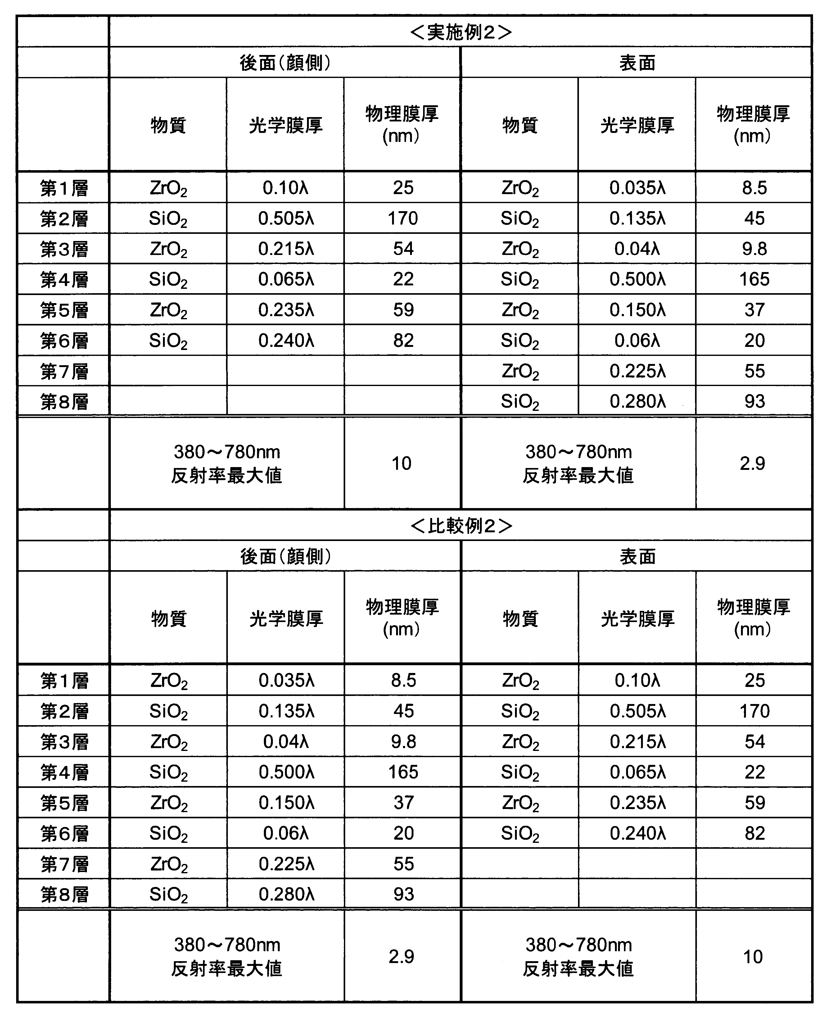

このようにして得られた光学物品の装用評価を行った。
(装用評価1:視認性、疲労感確認)
実施例1に沿って作製した光学部品を装備した眼鏡を装用し、パソコンによるデスクワーク時に装用し、比較例1に沿って作製した光学部品を装備した眼鏡との比較評価を行った。
評価時の条件及び、判定項目は以下の通りである。
モニタ人数 :12名
ディスプレイ:17インチ液晶ディスプレイ
作業時間 :1時間/日
装用期間 :1週間
判定項目 :1.表示文字等の見え易さ 2.疲労感
判定基準 :1.実施例が良い 2.同等 3.比較例が良い
判定基準の回答人数を集計し、装用評価1の結果を表2に示す。 Wear evaluation of the optical article thus obtained was performed.
(Wear evaluation 1: visibility, fatigue check)
The spectacles equipped with the optical parts produced according to Example 1 were worn and worn at the time of desk work by a personal computer, and the comparative evaluation with the spectacles equipped with the optical parts produced according to Comparative Example 1 was performed.
Conditions at the time of evaluation and judgment items are as follows.
Number of monitors: 12 people Display: 17-inch liquid crystal display work time: 1 hour / daily wear period: 1 week Judgment items: 1. Visibility of display characters etc. Fatigue criteria: 1. Good example.Equivalent 2. Good comparative example
Table 2 shows the results of wearingevaluation 1 by counting the number of respondents according to the criterion.
(装用評価1:視認性、疲労感確認)
実施例1に沿って作製した光学部品を装備した眼鏡を装用し、パソコンによるデスクワーク時に装用し、比較例1に沿って作製した光学部品を装備した眼鏡との比較評価を行った。
評価時の条件及び、判定項目は以下の通りである。
モニタ人数 :12名
ディスプレイ:17インチ液晶ディスプレイ
作業時間 :1時間/日
装用期間 :1週間
判定項目 :1.表示文字等の見え易さ 2.疲労感
判定基準 :1.実施例が良い 2.同等 3.比較例が良い
判定基準の回答人数を集計し、装用評価1の結果を表2に示す。 Wear evaluation of the optical article thus obtained was performed.
(Wear evaluation 1: visibility, fatigue check)
The spectacles equipped with the optical parts produced according to Example 1 were worn and worn at the time of desk work by a personal computer, and the comparative evaluation with the spectacles equipped with the optical parts produced according to Comparative Example 1 was performed.
Conditions at the time of evaluation and judgment items are as follows.
Number of monitors: 12 people Display: 17-inch liquid crystal display work time: 1 hour / daily wear period: 1 week Judgment items: 1. Visibility of display characters etc. Fatigue criteria: 1. Good example.
Table 2 shows the results of wearing
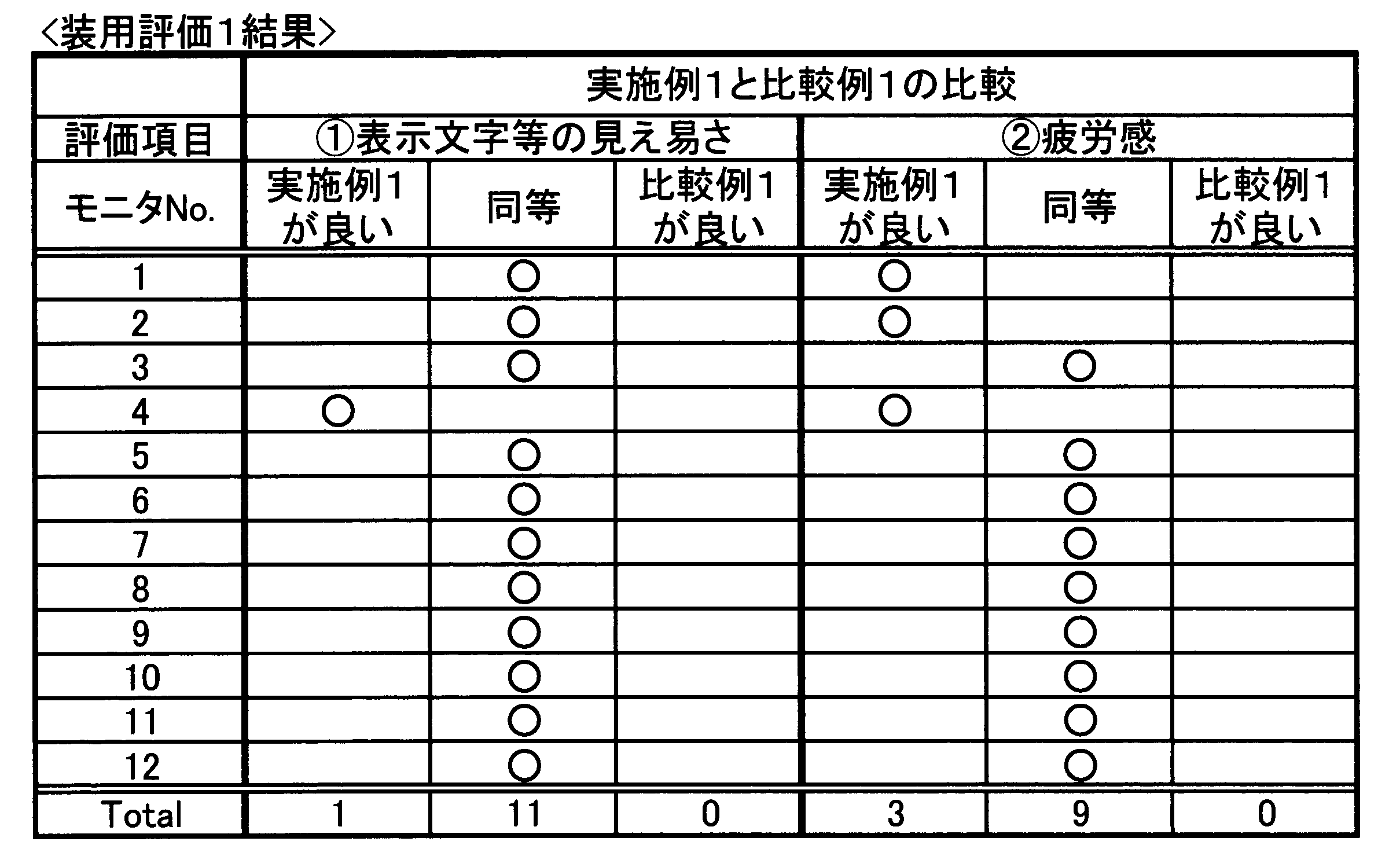
(装用評価2:入射光によるわずらわしさ等装用感比較)
実施例1~3及び比較例1~3に沿って作製した光学部品を装備した眼鏡を装用し、様々な環境下において入射光の影響の比較評価を行った。評価時の条件及び、判定項目は以下の通りである。
モニタ人数:12名
評価環境 :1.オフィス 2.日中電車内 3.夜間
装用期間 :1週間
判定項目 :1.天井灯の映りこみ 2.外光の映りこみ 3.街灯の映りこみ
判定基準 :1.実施例が良い 2.同等 3.比較例が良い
判定基準の回答人数を集計し、装用評価2の結果を表3に示す。 (Wearing evaluation 2: Comparison of wearing feeling such as annoyance by incident light)
Wearing spectacles equipped with optical parts produced according to Examples 1 to 3 and Comparative Examples 1 to 3, comparative evaluation of the influence of incident light was performed under various environments. Conditions at the time of evaluation and judgment items are as follows.
Number of monitors: 12 Evaluation environment: 1.Office 2. 2. Inside the train during the day At night
Wearing period: 1 week Judgment items: 1. 1. Reflection ofceiling light 2. Reflection of external light Criteria for reflecting on streetlights: 1. Good example. Equivalent 2. Good comparative example
Table 3 shows the results of wearingevaluation 2 by counting the number of respondents according to the criterion.
実施例1~3及び比較例1~3に沿って作製した光学部品を装備した眼鏡を装用し、様々な環境下において入射光の影響の比較評価を行った。評価時の条件及び、判定項目は以下の通りである。
モニタ人数:12名
評価環境 :1.オフィス 2.日中電車内 3.夜間
装用期間 :1週間
判定項目 :1.天井灯の映りこみ 2.外光の映りこみ 3.街灯の映りこみ
判定基準 :1.実施例が良い 2.同等 3.比較例が良い
判定基準の回答人数を集計し、装用評価2の結果を表3に示す。 (Wearing evaluation 2: Comparison of wearing feeling such as annoyance by incident light)
Wearing spectacles equipped with optical parts produced according to Examples 1 to 3 and Comparative Examples 1 to 3, comparative evaluation of the influence of incident light was performed under various environments. Conditions at the time of evaluation and judgment items are as follows.
Number of monitors: 12 Evaluation environment: 1.
Wearing period: 1 week Judgment items: 1. 1. Reflection of
Table 3 shows the results of wearing
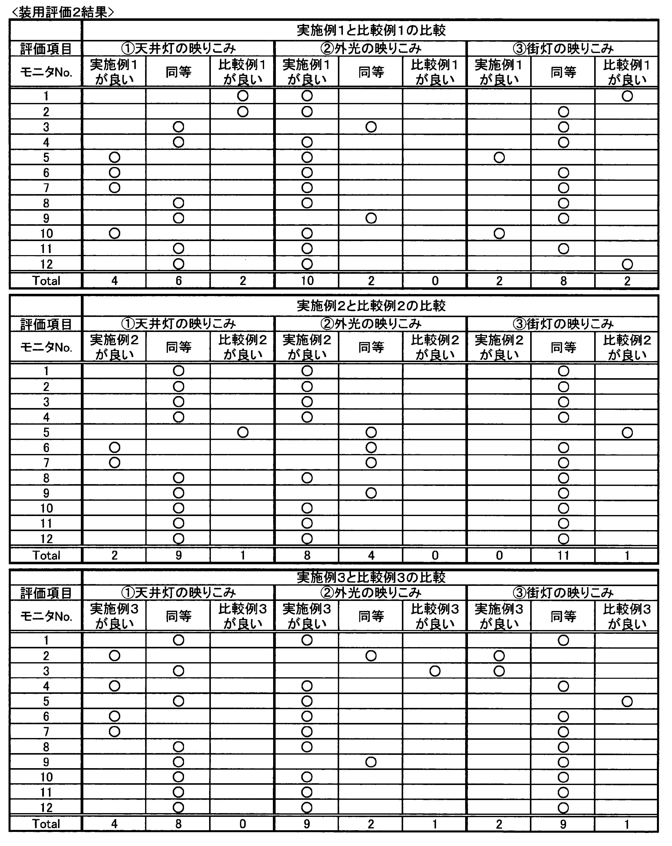
このような装用比較評価を行った結果、視認性、疲労感については実施例1と比較例1に差がないことが確認された。
入射光によるわずらわしさについては、外光の映りこみによるわずらわしさは実施例1、実施例2、実施例3が良いと回答した人数が多いことから、後面(顔側の面)に380~780nmの波長範囲における反射率の最大値が3~50%の多層膜を配設することにより入射光によるわずらわしさがなく、視認性が向上することが確認された。 As a result of performing such wearing comparative evaluation, it was confirmed that there was no difference between Example 1 and Comparative Example 1 in terms of visibility and fatigue.
Regarding the troublesomeness caused by incident light, since there are many people who answered that the troublesomeness caused by reflection of external light is good in Example 1, Example 2, and Example 3, 380 to 780 nm on the rear surface (face side). It was confirmed that by arranging a multilayer film having a maximum reflectance of 3 to 50% in the wavelength range, there is no troublesome incident light and visibility is improved.
≪実験2≫
合成樹脂基板上に、屈折率1.67のシリコン系ハードコートを加熱硬化にて施し、以下に示すように真空蒸着法により成膜した。
尚、ウレタン系合成樹脂基板として、実験1と同様に、度数が-1.00D~-6.00Dの範囲内にあり、表面の曲率半径が200mm~1300mmの範囲内にあり、後面の曲率半径が100mm~170mmの範囲内にあるものを使用した。ウレタン合成樹脂基板の度数は負であるため、各基板における後面の曲率半径は、表面の曲率半径より小さく、後面の曲率は、表面の曲率より大きいものとなっている。 ≪Experiment 2≫
On the synthetic resin substrate, a silicon hard coat having a refractive index of 1.67 was applied by heat curing, and a film was formed by vacuum deposition as shown below.
As in the case ofExperiment 1, the urethane-based synthetic resin substrate has a power in the range of -1.00D to -6.00D, a surface radius of curvature in the range of 200 mm to 1300 mm, and a curvature radius of the rear surface. In the range of 100 mm to 170 mm was used. Since the power of the urethane synthetic resin substrate is negative, the curvature radius of the rear surface of each substrate is smaller than the curvature radius of the surface, and the curvature of the rear surface is larger than the curvature of the surface.
合成樹脂基板上に、屈折率1.67のシリコン系ハードコートを加熱硬化にて施し、以下に示すように真空蒸着法により成膜した。
尚、ウレタン系合成樹脂基板として、実験1と同様に、度数が-1.00D~-6.00Dの範囲内にあり、表面の曲率半径が200mm~1300mmの範囲内にあり、後面の曲率半径が100mm~170mmの範囲内にあるものを使用した。ウレタン合成樹脂基板の度数は負であるため、各基板における後面の曲率半径は、表面の曲率半径より小さく、後面の曲率は、表面の曲率より大きいものとなっている。 ≪
On the synthetic resin substrate, a silicon hard coat having a refractive index of 1.67 was applied by heat curing, and a film was formed by vacuum deposition as shown below.
As in the case of
<実施例4>
後面(顔側):レンズを真空槽内に設けられた回転するドームにセットし、真空槽内の温度を70度に加熱し、圧力が1.0×10⁻³Paになるまで排気し、加速電圧500V、加速電流100mAの条件でArイオンビームクリーニングを60秒間施した後、プラスチック基材側から順次、第1層ZrO2(屈折率2.00)を光学的膜厚0.135λ、第2層SiO2(屈折率1.47)を光学的膜厚0.085λ、第3層ZrO2(屈折率2.00)を光学的膜厚0.20λ、第4層SiO2(屈折率1.47)を光学的膜厚0.055λ、第5層ZrO2(屈折率2.00)を光学的膜厚0.19λ、第6層SiO2(屈折率1.47)を光学的膜厚0.35λで積層した。尚、λは設計の中心波長で500nmとした。
表面:後面と同様の装置、加工雰囲気、前処理後、プラスチック基材側から順次、第1層ZrO2(屈折率2.00)を光学的膜厚0.11λ、第2層SiO2(屈折率1.47)を光学的膜厚0.09λ、第3層ZrO2(屈折率2.00)を光学的膜厚0.22λ、第4層SiO2(屈折率1.47)を光学的膜厚0.06λ、第5層ZrO2(屈折率2.00)を光学的膜厚0.20λ、第6層SiO2(屈折率1.47)を光学的膜厚0.33λで積層した。尚、λは設計の中心波長で500nmとした。 <Example 4>
Rear side (face side): Set the lens in a rotating dome provided in the vacuum chamber, heat the temperature in the vacuum chamber to 70 degrees, and exhaust until the pressure becomes 1.0 × 10 −3 Pa, After performing Ar ion beam cleaning for 60 seconds under conditions of an acceleration voltage of 500 V and an acceleration current of 100 mA, the first layer ZrO 2 (refractive index of 2.00) is sequentially applied from the plastic substrate side to an optical film thickness of 0.135λ, The second layer SiO 2 (refractive index 1.47) has an optical film thickness of 0.085λ, the third layer ZrO 2 (refractive index 2.00) has an optical film thickness of 0.20λ, and the fourth layer SiO 2 (refractive index 1). .47) has an optical thickness of 0.055λ, the fifth layer ZrO 2 (refractive index 2.00) has an optical thickness of 0.19λ, and the sixth layer SiO 2 (refractive index 1.47) has an optical thickness. Lamination was performed at 0.35λ. Note that λ is 500 nm as the design center wavelength.
Surface: Equipment similar to the rear surface, processing atmosphere, after pretreatment, and sequentially from the plastic substrate side, the first layer ZrO 2 (refractive index 2.00) has an optical film thickness of 0.11λ and the second layer SiO 2 (refractive The optical thickness is 0.09λ, the third layer ZrO 2 (refractive index 2.00) is optical thickness 0.22λ, and the fourth layer SiO 2 (refractive index 1.47) is optical. The film thickness was 0.06λ, the fifth layer ZrO 2 (refractive index 2.00) was laminated with an optical film thickness of 0.20λ, and the sixth layer SiO 2 (refractive index 1.47) was laminated with an optical film thickness of 0.33λ. . Note that λ is 500 nm as the design center wavelength.
<実施例5>
後面(顔側):レンズを真空槽内に設けられた回転するドームにセットし、真空槽内の温度を70度に加熱し、圧力が1.0×10⁻³Paになるまで排気し、加速電圧500V、加速電流100mAの条件でArイオンビームクリーニングを60秒間施した後、プラスチック基材側から順次、第1層ZrO2(屈折率2.00)を光学的膜厚0.11λ、第2層SiO2(屈折率1.47)を光学的膜厚0.09λ、第3層ZrO2(屈折率2.00)を光学的膜厚0.22λ、第4層SiO2(屈折率1.47)を光学的膜厚0.06λ、第5層ZrO2(屈折率2.00)を光学的膜厚0.20λ、第6層SiO2(屈折率1.47)を光学的膜厚0.33λで積層した。尚、λは設計の中心波長で500nmとした。
表面:後面と同様の装置、加工雰囲気、前処理後、プラスチック基材側から順次、第1層ZrO2(屈折率2.00)を光学的膜厚0.135λ、第2層SiO2(屈折率1.47)を光学的膜厚0.085λ、第3層ZrO2(屈折率2.00)を光学的膜厚0.20λ、第4層SiO2(屈折率1.47)を光学的膜厚0.055λ、第5層ZrO2(屈折率2.00)を光学的膜厚0.19λ、第6層SiO2(屈折率1.47)を光学的膜厚0.35λで積層した。尚、λは設計の中心波長で500nmとした。
実施例4のレンズの後面及び実施例5のレンズの表面における分光特性図及び分光特性データを図14A、14Bに示し、実施例4のレンズの表面及び実施例5のレンズの後面における分光特性図及び分光特性データを図15A、15Bに示す。 <Example 5>
Rear side (face side): Set the lens in a rotating dome provided in the vacuum chamber, heat the temperature in the vacuum chamber to 70 degrees, and exhaust until the pressure becomes 1.0 × 10 −3 Pa, After performing Ar ion beam cleaning for 60 seconds under conditions of an acceleration voltage of 500 V and an acceleration current of 100 mA, the first layer ZrO 2 (refractive index of 2.00) is sequentially applied from the plastic substrate side to an optical film thickness of 0.11λ, The second layer SiO 2 (refractive index 1.47) has an optical film thickness of 0.09λ, the third layer ZrO 2 (refractive index 2.00) has an optical film thickness of 0.22λ, and the fourth layer SiO 2 (refractive index 1). .47) has an optical thickness of 0.06λ, the fifth layer ZrO 2 (refractive index 2.00) has an optical thickness of 0.20λ, and the sixth layer SiO 2 (refractive index 1.47) has an optical thickness. Lamination was performed at 0.33λ. Note that λ is 500 nm as the design center wavelength.
Surface: Equipment similar to the rear surface, processing atmosphere, after pretreatment, and sequentially from the plastic substrate side, the first layer ZrO 2 (refractive index 2.00) has an optical film thickness of 0.135λ, and the second layer SiO 2 (refractive The optical thickness is 0.085λ, the third layer ZrO 2 (refractive index 2.00) is optical thickness 0.20λ, and the fourth layer SiO 2 (refractive index 1.47) is optical. A film thickness of 0.055λ, a fifth layer ZrO 2 (refractive index of 2.00) with an optical film thickness of 0.19λ, and a sixth layer of SiO 2 (refractive index of 1.47) with an optical film thickness of 0.35λ were laminated. . Note that λ is 500 nm as the design center wavelength.
Spectral characteristic diagrams and spectral characteristic data on the rear surface of the lens of Example 4 and the surface of the lens of Example 5 are shown in FIGS. 14A and 14B, and the spectral characteristic diagrams on the surface of the lens of Example 4 and the rear surface of the lens of Example 5. 15A and 15B show the spectral characteristic data.
実施例4及び実施例5における各成膜層の詳細を表4に示す。また、実施例4及び実施例5における透過特性図を図16A~17Aに、実施例4及び実施例5における透過特性データを図16B~17Bに示す。
Table 4 shows details of each film formation layer in Example 4 and Example 5. In addition, the transmission characteristic diagrams in Examples 4 and 5 are shown in FIGS. 16A to 17A, and the transmission characteristic data in Examples 4 and 5 are shown in FIGS. 16B to 17B.

このようにして得られた光学物品の装用評価を行った。
(装用評価1:視認性、疲労感確認)
実施例4に沿って作製した光学部品を装備した眼鏡を装用し、パソコンによるデスクワーク時に装用し、実施例5に沿って作製した光学部品を装備した眼鏡との比較評価を行った。
評価時の条件及び、判定項目は以下の通りである。
モニタ人数 :12名
ディスプレイ:17インチ液晶ディスプレイ
作業時間 :1時間/日
装用期間 :1週間
判定項目 :1.表示文字等の見え易さ 2.疲労感
判定基準 :1.実施例4が良い 2.同等 3.実施例5が良い
判定基準の回答人数を集計し、装用評価1の結果を表5及び図18に示す。 Wear evaluation of the optical article thus obtained was performed.
(Wear evaluation 1: visibility, fatigue check)
The spectacles equipped with the optical parts produced according to Example 4 were worn and worn at the time of desk work by a personal computer, and a comparative evaluation with the spectacles equipped with the optical parts produced according to Example 5 was performed.
Conditions at the time of evaluation and judgment items are as follows.
Number of monitors: 12 people Display: 17-inch liquid crystal display work time: 1 hour / daily wear period: 1 week Judgment items: 1. Visibility of display characters etc. Fatigue criteria: 1. Example 4 isgood Equivalent 2. Example 5 is good
The number of respondents according to the criterion is tabulated, and the results of wearingevaluation 1 are shown in Table 5 and FIG.
(装用評価1:視認性、疲労感確認)
実施例4に沿って作製した光学部品を装備した眼鏡を装用し、パソコンによるデスクワーク時に装用し、実施例5に沿って作製した光学部品を装備した眼鏡との比較評価を行った。
評価時の条件及び、判定項目は以下の通りである。
モニタ人数 :12名
ディスプレイ:17インチ液晶ディスプレイ
作業時間 :1時間/日
装用期間 :1週間
判定項目 :1.表示文字等の見え易さ 2.疲労感
判定基準 :1.実施例4が良い 2.同等 3.実施例5が良い
判定基準の回答人数を集計し、装用評価1の結果を表5及び図18に示す。 Wear evaluation of the optical article thus obtained was performed.
(Wear evaluation 1: visibility, fatigue check)
The spectacles equipped with the optical parts produced according to Example 4 were worn and worn at the time of desk work by a personal computer, and a comparative evaluation with the spectacles equipped with the optical parts produced according to Example 5 was performed.
Conditions at the time of evaluation and judgment items are as follows.
Number of monitors: 12 people Display: 17-inch liquid crystal display work time: 1 hour / daily wear period: 1 week Judgment items: 1. Visibility of display characters etc. Fatigue criteria: 1. Example 4 is
The number of respondents according to the criterion is tabulated, and the results of wearing

(装用評価2:入射光によるわずらわしさ等装用感比較)
実施例4及び実施例5に沿って作製した光学部品を装備した眼鏡を装用し、様々な環境下において入射光の影響の比較評価を行った。評価時の条件及び、判定項目は以下の通りである。
モニタ人数:12名
評価環境 :1.オフィス 2.日中電車内 3.夜間
装用期間 :1週間
判定項目 :1.天井灯の映りこみ 2.外光の映りこみ 3.街灯の映りこみ
判定基準 :1.実施例4が良い 2.同等 3.実施例5が良い
判定基準の回答人数を集計し、装用評価2の結果を表6及び図19に示す。 (Wearing evaluation 2: Comparison of wearing feeling such as annoyingness by incident light)
The spectacles equipped with the optical parts produced according to Example 4 and Example 5 were worn, and the comparative evaluation of the influence of incident light was performed under various environments. Conditions at the time of evaluation and judgment items are as follows.
Number of monitors: 12 Evaluation environment: 1.Office 2. 2. Inside the train during the day Night wearing period: 1 week Judgment items: 1. 1. Reflection of ceiling light 2. Reflection of external light Criteria for reflecting on streetlights: 1. Example 4 is good Equivalent 2. Example 5 is good
The number of respondents according to the criterion is tabulated, and the results of wearingevaluation 2 are shown in Table 6 and FIG.
実施例4及び実施例5に沿って作製した光学部品を装備した眼鏡を装用し、様々な環境下において入射光の影響の比較評価を行った。評価時の条件及び、判定項目は以下の通りである。
モニタ人数:12名
評価環境 :1.オフィス 2.日中電車内 3.夜間
装用期間 :1週間
判定項目 :1.天井灯の映りこみ 2.外光の映りこみ 3.街灯の映りこみ
判定基準 :1.実施例4が良い 2.同等 3.実施例5が良い
判定基準の回答人数を集計し、装用評価2の結果を表6及び図19に示す。 (Wearing evaluation 2: Comparison of wearing feeling such as annoyingness by incident light)
The spectacles equipped with the optical parts produced according to Example 4 and Example 5 were worn, and the comparative evaluation of the influence of incident light was performed under various environments. Conditions at the time of evaluation and judgment items are as follows.
Number of monitors: 12 Evaluation environment: 1.
The number of respondents according to the criterion is tabulated, and the results of wearing

このような装用比較評価を行った結果、視認性、疲労感については実施例4及び実施例5に差がないことが確認された。入射光によるわずらわしさについては、外光の映りこみによるわずらわしさは、実施例4及び実施例5の両方において、問題を生じないレベルであったが、両者を比較すると、実施例4が良いとの人数が多かった。
このことから、後面(顔側)に380~780nmの波長範囲における反射率の最大値が3~50%の多層膜を配設し、後面の反射率最大値を、表面の反射率最大値よりも大きくすることにより、入射光によるわずらわしさがなく、視認性が向上することが確認された。 As a result of such comparative wearing evaluation, it was confirmed that there was no difference between Example 4 and Example 5 in terms of visibility and fatigue. Regarding the troublesomeness caused by incident light, the troublesomeness caused by the reflection of external light was at a level that would not cause a problem in both Example 4 and Example 5, but when both were compared, Example 4 was good. There were a lot of people.
For this reason, a multilayer film having a maximum reflectance of 3 to 50% in the wavelength range of 380 to 780 nm is disposed on the rear surface (face side), and the maximum reflectance on the rear surface is greater than the maximum reflectance on the surface. It was confirmed that by increasing the size, visibility is improved without the trouble of incident light.
また、反射光の収束のシミュレーションによると、曲率半径200mmのレンズ後面で反射した光が眼に収束する量を基準とした場合、曲率半径250mmで1.3倍、350mmで1.5倍、1300mmでは1.7倍との結果が得られている。
このような数値からも、負の度数のレンズにおいて、曲率が大きい後面に、曲率が小さい表面よりも380~780nmの波長範囲における反射率の最大値が大きい多層膜を配設することにより、入射光によるわずらわしさがなく、視認性が向上することが明らかである。 Further, according to the simulation of reflected light convergence, when the amount of light reflected by the rear surface of the lens having a curvature radius of 200 mm is converged on the eye, the curvature radius is 1.3 times at 250 mm, 1.5 times at 350 mm, and 1300 mm. The result of 1.7 times is obtained.
Even from such numerical values, in a negative power lens, a multi-layer film having a maximum reflectance in a wavelength range of 380 to 780 nm is disposed on the rear surface having a large curvature than the surface having a small curvature. It is clear that the visibility is improved without the trouble of light.
以上の結果から、本発明の態様によれば、防眩効果等のフィルター機能を有し、装用による疲労感も無く、かつ、視認性が良好な光学部品及びその製造方法を提供できることが明らかである。
From the above results, it is clear that according to the aspect of the present invention, it is possible to provide an optical component having a filter function such as an antiglare effect, no fatigue feeling due to wearing, and good visibility, and a method for manufacturing the same. is there.
1,1’…光学部品、2…プラスチック基材、3,3’…無機多層膜、4…機能性薄膜、5…プライマー層(機能性薄膜)、6…ハードコート層(機能性薄膜)、7,7’…高屈折率層、8,8’…低屈折率層、9,9’…第1層、10,10’…第2層、11,11’…第3層、12…撥水撥油膜、30…蒸着装置、30’… 成膜装置、31…第1成膜室、32…第2成膜室、33…第3成膜室、34…保持部材、35,35’…蒸着源、35A…第1蒸着源、35B…第2蒸着源、36…光源装置、37…イオンガン。
DESCRIPTION OF SYMBOLS 1,1 '... Optical component, 2 ... Plastic base material, 3, 3' ... Inorganic multilayer film, 4 ... Functional thin film, 5 ... Primer layer (functional thin film), 6 ... Hard-coat layer (functional thin film), 7, 7 '... high refractive index layer, 8, 8' ... low refractive index layer, 9, 9 '... first layer, 10, 10' ... second layer, 11, 11 '... third layer, 12 ... repellent Water / oil repellent film, 30 ... deposition device, 30 '... soot film forming device, 31 ... first film forming chamber, 32 ... second film forming chamber, 33 ... third film forming chamber, 34 ... holding member, 35, 35' ... Deposition source, 35A ... first deposition source, 35B ... second deposition source, 36 ... light source device, 37 ... ion gun.
Claims (27)
- プラスチック基材と、前記プラスチック基材の表面と後面のうち、少なくとも曲率の大きい方の面上に配設された多層膜とを備えた光学部品であって、
前記多層膜は、380~780nmの波長範囲における反射率最大値が3~50%であることを特徴とする光学部品。 An optical component comprising a plastic substrate and a multilayer film disposed on at least one of the surfaces having the larger curvature among the surface and rear surface of the plastic substrate,
The multilayer film has an optical reflectance maximum value of 3 to 50% in a wavelength range of 380 to 780 nm. - 前記プラスチック基材の度数が負である請求項1に記載の光学部品。 The optical component according to claim 1, wherein the plastic substrate has a negative power.
- 前記曲率の大きい方の面上に配設された多層膜の前記反射率最大値は、曲率の小さい方の面上に配設された多層膜の前記反射率最大値よりも大きい請求項1又は2に記載の光学部品。 The maximum reflectance of the multilayer film disposed on the surface with the larger curvature is larger than the maximum reflectance of the multilayer film disposed on the surface with the smaller curvature. 2. The optical component according to 2.
- 前記曲率の大きい方の面上に配設された多層膜の前記反射率最大値と、前記曲率の小さい方の面上に配設された多層膜の前記反射率最大値との差が2~49%である請求項1~3のいずれか一項に記載の光学部品。 The difference between the maximum reflectance value of the multilayer film disposed on the surface with the larger curvature and the maximum reflectance value of the multilayer film disposed on the surface with the smaller curvature is 2 to The optical component according to any one of claims 1 to 3, which is 49%.
- 前記曲率の小さい方の面上に380~780nmの波長範囲における平均反射率が5.0%以下の反射防止膜が配設された請求項1~4のいずれか一項に記載の光学部品。 The optical component according to any one of claims 1 to 4, wherein an antireflection film having an average reflectance of 5.0% or less in a wavelength range of 380 to 780 nm is disposed on the surface having the smaller curvature.
- 前記プラスチック基材は、着色され、その透過率が5~85%である請求項1~5のいずれか一項に記載の光学部品。 The optical component according to any one of claims 1 to 5, wherein the plastic substrate is colored and has a transmittance of 5 to 85%.
- 前記プラスチック基材から最も遠い前記多層膜の最外層の上に、フッ素置換アルキル基含有有機ケイ素化合物を含む撥水撥油膜を更に備える請求項1~6のいずれか一項に記載の光学部品。 The optical component according to any one of claims 1 to 6, further comprising a water / oil repellent film containing a fluorine-substituted alkyl group-containing organosilicon compound on the outermost layer of the multilayer film farthest from the plastic substrate.
- 前記フッ素置換アルキル基含有有機ケイ素化合物は、下記一般式(1):

及び下記一般式(2)~(5):
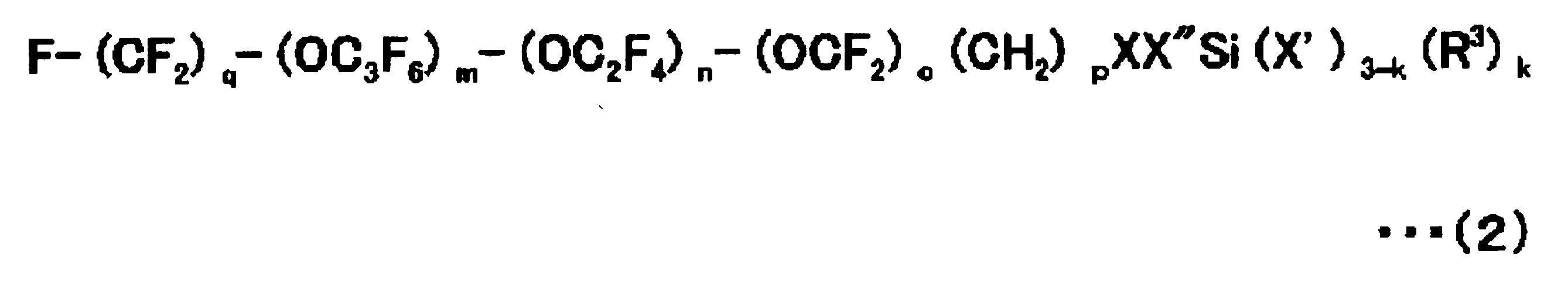


及び下記一般式(6):
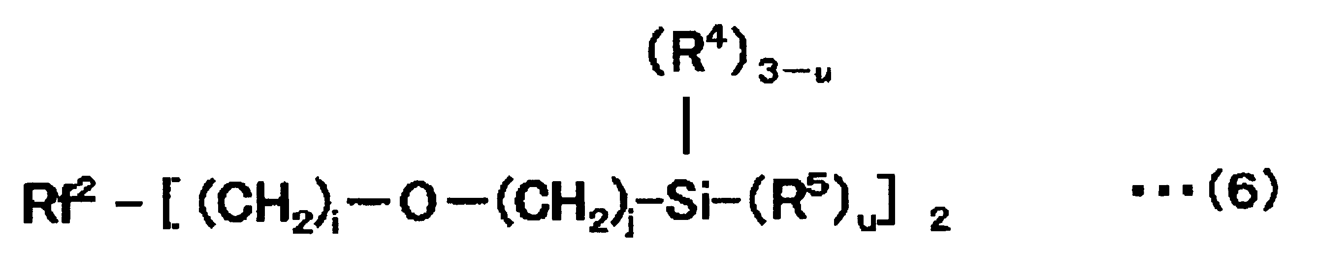
の中から選択される1種類以上のフッ素置換アルキル基含有有機ケイ素化合物である請求項7に記載の光学部品。 The fluorine-substituted alkyl group-containing organosilicon compound has the following general formula (1):
And the following general formulas (2) to (5):
And the following general formula (6):
The optical component according to claim 7, which is one or more fluorine-substituted alkyl group-containing organosilicon compounds selected from the group consisting of: - 前記多層膜は、4層以上の多層膜である請求項1~8のいずれか一項に記載の光学部品。 The optical component according to any one of claims 1 to 8, wherein the multilayer film is a multilayer film having four or more layers.
- 前記プラスチック基材と前記多層膜との間に、機能性薄膜を備えたことを特徴とする請求項1~9のいずれか一項に記載の光学部品。 10. The optical component according to claim 1, wherein a functional thin film is provided between the plastic substrate and the multilayer film.
- 前記多層膜を構成する高屈折率材料と低屈折率材料との間に、厚さ20nm以下の誘電体膜又は金属膜を備えたことを特徴とする請求項1~10のいずれか一項に記載の光学部品。 11. A dielectric film or a metal film having a thickness of 20 nm or less is provided between a high refractive index material and a low refractive index material constituting the multilayer film. The optical component described.
- 前記高屈折率材料は、二酸化ジルコニウムを含み、前記低屈折率材料は、二酸化珪素を含むことを特徴とする請求項1~11のいずれか一項に記載の光学部品。 The optical component according to any one of claims 1 to 11, wherein the high refractive index material includes zirconium dioxide, and the low refractive index material includes silicon dioxide.
- 眼鏡レンズ用である請求項1~12のいずれか一項に記載の光学部品。 The optical component according to any one of claims 1 to 12, which is used for eyeglass lenses.
- プラスチック基材と、前記プラスチック基材の表面と後面のうち、少なくとも曲率の大きい方の面上に配設された多層膜とを備えた光学部品の製造方法であって、
前記プラスチック基材を加熱する工程と、前記加熱によって前記プラスチック基材を所定温度に調整した後、前記プラスチック基材上に前記多層膜を形成する工程とを備え、
前記多層膜を形成する工程は、高屈折率材料と低屈折率材料とを交互に複数積層し多層構造の高屈折率層を形成する処理と、前記高屈折率層上に、この高屈折率層より低い屈折率の低屈折率材料からなる低屈折率層を形成する処理と、を有するとともに、
前記多層膜の380~780nmの波長範囲における反射率最大値を3~50%にすることを特徴とする請求項1~13のいずれか一項に記載の光学部品の製造方法。 A method of manufacturing an optical component comprising: a plastic substrate; and a multilayer film disposed on at least a surface having a larger curvature among the surface and the rear surface of the plastic substrate,
The step of heating the plastic substrate, and the step of forming the multilayer film on the plastic substrate after adjusting the plastic substrate to a predetermined temperature by the heating,
The step of forming the multilayer film includes a process of alternately stacking a plurality of high refractive index materials and low refractive index materials to form a high refractive index layer having a multilayer structure, and the high refractive index layer on the high refractive index layer. Forming a low refractive index layer made of a low refractive index material having a lower refractive index than the layer, and
14. The method of manufacturing an optical component according to claim 1, wherein the maximum reflectance of the multilayer film in a wavelength range of 380 to 780 nm is set to 3 to 50%. - 前記多層膜を、真空蒸着法を用いて形成する工程を含む請求項14に記載の光学部品の製造方法。 The method for manufacturing an optical component according to claim 14, comprising a step of forming the multilayer film using a vacuum deposition method.
- 前記多層膜を形成する工程は、前記多層膜を構成する層のうちの少なくとも一層を、イオンビームアシストを施しながら成膜を行う工程を含む請求項14又は15に記載の光学部品の製造方法。 The method of manufacturing an optical component according to claim 14 or 15, wherein the step of forming the multilayer film includes a step of forming a film while performing ion beam assist on at least one of the layers constituting the multilayer film.
- 前記イオンビームアシストは、不活性ガス、酸素ガス、及び、不活性ガスと酸素ガスの混合ガスのうちから選ばれる少なくとも一種のガスを用いて行われる請求項16に記載の光学部品の製造方法。 The method of manufacturing an optical component according to claim 16, wherein the ion beam assist is performed using at least one gas selected from an inert gas, an oxygen gas, and a mixed gas of an inert gas and an oxygen gas.
- 前記不活性ガスはアルゴンである請求項17に記載の光学部品の製造方法。 The method for manufacturing an optical component according to claim 17, wherein the inert gas is argon.
- 表面及び後面を有するプラスチック基材と、
前記表面に設けられた第1多層膜であり、380nm以上かつ780nm以内の波長範囲における平均反射率が3%以下である、前記第1多層膜と、
前記後面に設けられた第2多層膜であり、415nm以上かつ780nm以内の波長範囲のうち、極大値の反射率の第1波長を含む30nmの範囲における平均反射率が2%以上かつ13%以内である、前記第2多層膜と、
を備える眼鏡レンズ。 A plastic substrate having a front surface and a rear surface;
The first multilayer film provided on the surface, and having an average reflectance of 3% or less in a wavelength range of 380 nm to 780 nm;
The second multilayer film provided on the rear surface, wherein the average reflectance in the range of 30 nm including the first wavelength of the maximum reflectance in the wavelength range of 415 nm or more and 780 nm or less is 2% or more and 13% or less. The second multilayer film,
Eyeglass lens with - 前記第1波長における、前記第1多層膜の反射率と前記第2多層膜の反射率との差が1%以上かつ10%以内である、請求項19に記載の眼鏡レンズ。 The spectacle lens according to claim 19, wherein a difference between the reflectance of the first multilayer film and the reflectance of the second multilayer film at the first wavelength is 1% or more and 10% or less.
- 表面及び後面を有するプラスチック基材と、
前記表面に設けられた第1多層膜であり、380nm以上かつ780nm以内の波長範囲における平均反射率が3%未満である、前記第1多層膜と、
前記後面に設けられた第2多層膜であり、380nm以上かつ500nm以内の波長範囲のうちの反射率が最大となる第1波長を含む30nmの範囲における平均反射率が3%以上かつ30%以内である、前記第2多層膜と、
を備える眼鏡レンズ。 A plastic substrate having a front surface and a rear surface;
The first multilayer film provided on the surface, the first multilayer film having an average reflectance of less than 3% in a wavelength range of 380 nm or more and 780 nm or less;
The second multilayer film provided on the rear surface, wherein the average reflectance in the range of 30 nm including the first wavelength in the wavelength range of 380 nm or more and 500 nm or less including the first wavelength is 3% or more and 30% or less. The second multilayer film,
Eyeglass lens with - 前記第1波長における、前記第1多層膜の反射率と前記第2多層膜の反射率との差が3%以上かつ41%以内である、請求項21に記載の眼鏡レンズ。 The spectacle lens according to claim 21, wherein a difference between the reflectance of the first multilayer film and the reflectance of the second multilayer film at the first wavelength is 3% or more and 41% or less.
- 前記第1多層膜は、380nm以上かつ780nm以内の波長範囲における平均反射率が1.5%未満であり、380nm以上かつ500nm以内の波長範囲における平均反射率が3%未満である、請求項21又は22に記載の眼鏡レンズ。 The first multilayer film has an average reflectance of less than 1.5% in a wavelength range of 380 nm to 780 nm and an average reflectance of less than 3% in a wavelength range of 380 nm to 500 nm. Or the spectacle lens of 22.
- 前記表面に設けられ、380nm以上かつ780nm以内の波長範囲における平均反射率が5.0%以下の反射防止膜をさらに備える、請求項21~23のいずれか一項に記載の眼鏡レンズ。 The spectacle lens according to any one of claims 21 to 23, further comprising an antireflection film provided on the surface and having an average reflectance of 5.0% or less in a wavelength range of 380 nm to 780 nm.
- 前記プラスチック基材は、着色され、その透過率が5%以上かつ85%以内である請求項21~24のいずれか一項に記載の眼鏡レンズ。 The spectacle lens according to any one of claims 21 to 24, wherein the plastic substrate is colored and has a transmittance of 5% or more and 85% or less.
- 前記プラスチック基材から最も遠い前記多層膜の最外層の上に、フッ素置換アルキル基含有有機ケイ素化合物を含む撥水撥油膜を更に備える請求項21~25のいずれか一項に記載の眼鏡レンズ。 The spectacle lens according to any one of claims 21 to 25, further comprising a water / oil repellent film containing a fluorine-substituted alkyl group-containing organosilicon compound on the outermost layer of the multilayer film farthest from the plastic substrate.
- プラスチック基材を加熱する工程と、
加熱された前記プラスチック基材に多層膜を形成する工程であり、
高屈折率材料の層と低屈折率材料の層とを有する多層構造の高屈折率層を形成する処理と、前記高屈折率層に比べて屈折率が低い低屈折率層を形成する処理と、を有し、
表面設けられた第1多層膜が、380nm以上かつ780nm以内の波長範囲における平均反射率が3%未満であり、
後面に設けられた第2多層膜が、380nm以上かつ500nm以内の波長範囲のうちの反射率が最大となる第1波長を含む30nmの範囲における平均反射率が3%以上かつ30%以内である、前記工程と、
を備える眼鏡レンズの製造方法。 Heating the plastic substrate;
Forming a multilayer film on the heated plastic substrate;
A process of forming a high refractive index layer having a multilayer structure having a layer of a high refractive index material and a layer of a low refractive index material; and a process of forming a low refractive index layer having a refractive index lower than that of the high refractive index layer Have
The first multilayer film provided on the surface has an average reflectance of less than 3% in a wavelength range of 380 nm or more and 780 nm or less,
The second multilayer film provided on the rear surface has an average reflectance of 3% or more and 30% or less in a range of 30 nm including the first wavelength in which the reflectance is maximum in a wavelength range of 380 nm or more and 500 nm or less. , The process,
A method of manufacturing a spectacle lens comprising:
Priority Applications (3)
| Application Number | Priority Date | Filing Date | Title |
|---|---|---|---|
| EP13749054.6A EP2816379A4 (en) | 2012-02-17 | 2013-02-18 | Optical component, spectacle lens, and manufacturing methods therefor |
| CN201380009514.7A CN104115037B (en) | 2012-02-17 | 2013-02-18 | Optics, eyeglass lens and manufacture method thereof |
| US14/457,544 US20140347625A1 (en) | 2012-02-17 | 2014-08-12 | Optical Component, Spectacle Lens, and Method of Manufacturing the Same |
Applications Claiming Priority (2)
| Application Number | Priority Date | Filing Date | Title |
|---|---|---|---|
| JP2012033167 | 2012-02-17 | ||
| JP2012-033167 | 2012-02-17 |
Related Child Applications (1)
| Application Number | Title | Priority Date | Filing Date |
|---|---|---|---|
| US14/457,544 Continuation US20140347625A1 (en) | 2012-02-17 | 2014-08-12 | Optical Component, Spectacle Lens, and Method of Manufacturing the Same |
Publications (1)
| Publication Number | Publication Date |
|---|---|
| WO2013122253A1 true WO2013122253A1 (en) | 2013-08-22 |
Family
ID=48984360
Family Applications (1)
| Application Number | Title | Priority Date | Filing Date |
|---|---|---|---|
| PCT/JP2013/053876 WO2013122253A1 (en) | 2012-02-17 | 2013-02-18 | Optical component, spectacle lens, and manufacturing methods therefor |
Country Status (5)
| Country | Link |
|---|---|
| US (1) | US20140347625A1 (en) |
| EP (1) | EP2816379A4 (en) |
| JP (2) | JP5625127B2 (en) |
| CN (1) | CN104115037B (en) |
| WO (1) | WO2013122253A1 (en) |
Cited By (9)
| Publication number | Priority date | Publication date | Assignee | Title |
|---|---|---|---|---|
| CN105378512A (en) * | 2013-08-28 | 2016-03-02 | 东海光学株式会社 | Optical product and spectacle lens |
| WO2016088763A1 (en) * | 2014-12-01 | 2016-06-09 | ホヤ レンズ タイランド リミテッド | Eyeglass lens and eyeglasses |
| CN107077010A (en) * | 2014-10-17 | 2017-08-18 | 豪雅镜片泰国有限公司 | eyeglass and glasses |
| JP2018503129A (en) * | 2015-01-07 | 2018-02-01 | ローデンシュトック ゲーエムベーハー | Layer system and optical element comprising the layer system |
| US20180067339A1 (en) * | 2015-05-11 | 2018-03-08 | Nikon-Essilor Co., Ltd. | Spectacle lens |
| WO2019009127A1 (en) * | 2017-07-03 | 2019-01-10 | 東海光学株式会社 | Optical plastic product, and plastic spectacle lenses and spectacles |
| JP2019059986A (en) * | 2017-09-27 | 2019-04-18 | 吉田 國雄 | Method for forming thin film, and optical element |
| US11526030B2 (en) | 2017-11-24 | 2022-12-13 | Hoya Lens Thailand Ltd. | Spectacle lens and spectacles |
| JP7364665B2 (en) | 2018-09-20 | 2023-10-18 | エシロール・アンテルナシオナル | Optical device with reduced reflection in deep red, near infrared and visible ranges |
Families Citing this family (24)
| Publication number | Priority date | Publication date | Assignee | Title |
|---|---|---|---|---|
| US9291746B2 (en) * | 2014-02-25 | 2016-03-22 | iCoat Company, LLC | Visible spectrum anti-reflective coatings with reduced reflections in ultraviolet and infrared spectral bands |
| EP3040761B1 (en) * | 2014-12-30 | 2020-04-01 | Essilor International | Ophthalmic anti-somnolence lens, device, and method |
| CN104597621A (en) * | 2015-02-10 | 2015-05-06 | 光驰科技(上海)有限公司 | Double-faced film-plated blue-light-proof resin lens |
| CA2980015C (en) * | 2015-03-18 | 2023-08-22 | Vision Ease, Lp | Crazing resistant coating and method thereof |
| JP6547948B2 (en) * | 2015-07-07 | 2019-07-24 | ミツミ電機株式会社 | Foreign object adhesion preventing device and camera device provided with the same |
| US20170066684A1 (en) | 2015-09-08 | 2017-03-09 | Corning Incorporated | Optical coatings including buffer layers |
| US20170097521A1 (en) * | 2015-10-01 | 2017-04-06 | Tokai Optical Co., Ltd. | Optical product and spectacle lens |
| CN105334641B (en) * | 2015-12-15 | 2018-04-03 | 南昌益盾科技有限公司 | A kind of anti-blue light eyeglass |
| CN105372838B (en) * | 2015-12-15 | 2018-05-04 | 龙南县生产力促进中心 | A kind of eyeglass with compound anti-blue light film layer |
| CN105301798B (en) * | 2015-12-15 | 2018-04-03 | 南昌益盾科技有限公司 | A kind of anti-blue light optical mirror slip |
| US10191305B2 (en) | 2015-12-30 | 2019-01-29 | Signet Armorlite, Inc. | Ophthalmic lens |
| KR20180078328A (en) * | 2016-08-22 | 2018-07-09 | 호야 렌즈 타일랜드 리미티드 | Spectacle lenses and glasses |
| WO2019064771A1 (en) * | 2017-09-29 | 2019-04-04 | 日本電産株式会社 | Lens, lens unit and imaging device |
| EP3884315B1 (en) * | 2018-11-19 | 2024-01-03 | Essilor International | Optical lens having an enhanced interferential coating and a multilayer system for improving abrasion-resistance |
| WO2020104381A2 (en) * | 2018-11-19 | 2020-05-28 | Essilor International | Optical lens having a mirror coating and a multilayer system for improving abrasion-resistance |
| EP3654072A1 (en) * | 2018-11-19 | 2020-05-20 | Essilor International | Optical lens having a filtering interferential coating and a multilayer system for improving abrasion-resistance |
| EP3654071A1 (en) * | 2018-11-19 | 2020-05-20 | Essilor International | Optical lens having an interferential coating and a multilayer system for improving abrasion-resistance |
| US11678975B2 (en) | 2019-04-05 | 2023-06-20 | Amo Groningen B.V. | Systems and methods for treating ocular disease with an intraocular lens and refractive index writing |
| US11564839B2 (en) | 2019-04-05 | 2023-01-31 | Amo Groningen B.V. | Systems and methods for vergence matching of an intraocular lens with refractive index writing |
| US11529230B2 (en) | 2019-04-05 | 2022-12-20 | Amo Groningen B.V. | Systems and methods for correcting power of an intraocular lens using refractive index writing |
| US11583388B2 (en) | 2019-04-05 | 2023-02-21 | Amo Groningen B.V. | Systems and methods for spectacle independence using refractive index writing with an intraocular lens |
| US11583389B2 (en) | 2019-04-05 | 2023-02-21 | Amo Groningen B.V. | Systems and methods for correcting photic phenomenon from an intraocular lens and using refractive index writing |
| US11944574B2 (en) | 2019-04-05 | 2024-04-02 | Amo Groningen B.V. | Systems and methods for multiple layer intraocular lens and using refractive index writing |
| CN115373055A (en) * | 2021-05-17 | 2022-11-22 | 大永真空设备股份有限公司 | Optical multilayer film and use thereof |
Citations (11)
| Publication number | Priority date | Publication date | Assignee | Title |
|---|---|---|---|---|
| JPH03102301A (en) * | 1989-09-18 | 1991-04-26 | Kuraray Co Ltd | Method for evaluating characteristic of antireflection film and method for designing this film |
| JPH0455615B2 (en) | 1986-06-30 | 1992-09-03 | Hoya Corp | |
| JPH1130705A (en) * | 1997-05-16 | 1999-02-02 | Hoya Corp | Spectacle plastic lens with reflection preventive film |
| JPH1130703A (en) | 1997-05-16 | 1999-02-02 | Hoya Corp | Plastic optical parts having antireflection film |
| JP2002296406A (en) * | 2001-03-29 | 2002-10-09 | Sumitomo Chem Co Ltd | Antireflection base material with few reflection interference color |
| JP2004035941A (en) * | 2002-07-03 | 2004-02-05 | Konica Minolta Holdings Inc | Surface treatment method and optical component |
| JP2004151698A (en) * | 2002-10-07 | 2004-05-27 | Tdk Corp | Hologram recording medium |
| JP2006251760A (en) | 2005-02-08 | 2006-09-21 | Seiko Epson Corp | Optical component and method for manufacturing the same |
| JP2007127681A (en) | 2005-11-01 | 2007-05-24 | Tokai Kogaku Kk | Plastic lens |
| JP2007322572A (en) * | 2006-05-31 | 2007-12-13 | Omron Corp | Anti-reflection optical element |
| JP2012022081A (en) * | 2010-07-13 | 2012-02-02 | Keio Gijuku | Optical thin film, production method of the same, and optical multilayer film |
Family Cites Families (7)
| Publication number | Priority date | Publication date | Assignee | Title |
|---|---|---|---|---|
| US6250758B1 (en) * | 1997-05-16 | 2001-06-26 | Hoya Corporation | Plastic optical devices having antireflection film and mechanism for equalizing thickness of antireflection film |
| JP4524877B2 (en) * | 2000-07-17 | 2010-08-18 | コニカミノルタホールディングス株式会社 | Eyeglass lenses |
| FR2866643B1 (en) * | 2004-02-24 | 2006-05-26 | Saint Gobain | SUBSTRATE, ESPECIALLY GLASS, WITH A HYDROPHOBIC SURFACE, WITH IMPROVED DURABILITY OF HYDROPHOBIC PROPERTIES |
| WO2009041580A1 (en) * | 2007-09-28 | 2009-04-02 | Nikon-Essilor Co., Ltd. | Optical component and manufacturing method of the optical component |
| JPWO2010016242A1 (en) * | 2008-08-04 | 2012-01-19 | 株式会社ニコン・エシロール | Optical component and method for manufacturing optical component |
| JP2012073590A (en) * | 2010-08-31 | 2012-04-12 | Canon Inc | Optical member, production method of the same, and optical system |
| FR2968774B1 (en) * | 2010-12-10 | 2013-02-08 | Essilor Int | OPTICAL ARTICLE COMPRISING A LOW REFLECTIVE ANTIREFLECTION COATING IN THE ULTRAVIOLET DOMAIN AND THE VISIBLE DOMAIN |
-
2013
- 2013-02-18 JP JP2013558768A patent/JP5625127B2/en active Active
- 2013-02-18 EP EP13749054.6A patent/EP2816379A4/en not_active Withdrawn
- 2013-02-18 CN CN201380009514.7A patent/CN104115037B/en active Active
- 2013-02-18 WO PCT/JP2013/053876 patent/WO2013122253A1/en active Application Filing
-
2014
- 2014-08-12 US US14/457,544 patent/US20140347625A1/en not_active Abandoned
- 2014-10-02 JP JP2014204327A patent/JP5795675B2/en active Active
Patent Citations (11)
| Publication number | Priority date | Publication date | Assignee | Title |
|---|---|---|---|---|
| JPH0455615B2 (en) | 1986-06-30 | 1992-09-03 | Hoya Corp | |
| JPH03102301A (en) * | 1989-09-18 | 1991-04-26 | Kuraray Co Ltd | Method for evaluating characteristic of antireflection film and method for designing this film |
| JPH1130705A (en) * | 1997-05-16 | 1999-02-02 | Hoya Corp | Spectacle plastic lens with reflection preventive film |
| JPH1130703A (en) | 1997-05-16 | 1999-02-02 | Hoya Corp | Plastic optical parts having antireflection film |
| JP2002296406A (en) * | 2001-03-29 | 2002-10-09 | Sumitomo Chem Co Ltd | Antireflection base material with few reflection interference color |
| JP2004035941A (en) * | 2002-07-03 | 2004-02-05 | Konica Minolta Holdings Inc | Surface treatment method and optical component |
| JP2004151698A (en) * | 2002-10-07 | 2004-05-27 | Tdk Corp | Hologram recording medium |
| JP2006251760A (en) | 2005-02-08 | 2006-09-21 | Seiko Epson Corp | Optical component and method for manufacturing the same |
| JP2007127681A (en) | 2005-11-01 | 2007-05-24 | Tokai Kogaku Kk | Plastic lens |
| JP2007322572A (en) * | 2006-05-31 | 2007-12-13 | Omron Corp | Anti-reflection optical element |
| JP2012022081A (en) * | 2010-07-13 | 2012-02-02 | Keio Gijuku | Optical thin film, production method of the same, and optical multilayer film |
Non-Patent Citations (1)
| Title |
|---|
| See also references of EP2816379A4 |
Cited By (19)
| Publication number | Priority date | Publication date | Assignee | Title |
|---|---|---|---|---|
| CN105378512A (en) * | 2013-08-28 | 2016-03-02 | 东海光学株式会社 | Optical product and spectacle lens |
| CN107077010A (en) * | 2014-10-17 | 2017-08-18 | 豪雅镜片泰国有限公司 | eyeglass and glasses |
| US11402666B2 (en) | 2014-10-17 | 2022-08-02 | Hoya Lens Thailand Ltd. | Spectacle lens and spectacles |
| US10690944B2 (en) | 2014-12-01 | 2020-06-23 | Hoya Lens Thailand Ltd. | Spectacle lens that reflects blue light, and spectacles equipped with the spectacle lens |
| WO2016088763A1 (en) * | 2014-12-01 | 2016-06-09 | ホヤ レンズ タイランド リミテッド | Eyeglass lens and eyeglasses |
| JP7021156B2 (en) | 2015-01-07 | 2022-02-16 | ローデンシュトック ゲーエムベーハー | Optical elements with layered systems and layered systems |
| JP2019207424A (en) * | 2015-01-07 | 2019-12-05 | ローデンシュトック ゲーエムベーハー | Layer system and optical element comprising layer system |
| JP2018503129A (en) * | 2015-01-07 | 2018-02-01 | ローデンシュトック ゲーエムベーハー | Layer system and optical element comprising the layer system |
| US10459124B2 (en) | 2015-01-07 | 2019-10-29 | Rodenstock Gmbh | Layer system and optical element comprising a layer system |
| US20180067339A1 (en) * | 2015-05-11 | 2018-03-08 | Nikon-Essilor Co., Ltd. | Spectacle lens |
| US10908436B2 (en) * | 2015-05-11 | 2021-02-02 | Nikon-Essilor Co., Ltd. | Spectacle lens |
| WO2019009127A1 (en) * | 2017-07-03 | 2019-01-10 | 東海光学株式会社 | Optical plastic product, and plastic spectacle lenses and spectacles |
| JP2019015764A (en) * | 2017-07-03 | 2019-01-31 | 東海光学株式会社 | Plastic optical product, plastic spectacle lens and spectacles |
| US11709292B2 (en) | 2017-07-03 | 2023-07-25 | Tokai Optical Co., Ltd. | Optical plastic product, and plastic spectacle lens and spectacles |
| JP7041424B2 (en) | 2017-09-27 | 2022-03-24 | 國雄 吉田 | Thin film formation method and optical elements |
| JP2019059986A (en) * | 2017-09-27 | 2019-04-18 | 吉田 國雄 | Method for forming thin film, and optical element |
| US11526030B2 (en) | 2017-11-24 | 2022-12-13 | Hoya Lens Thailand Ltd. | Spectacle lens and spectacles |
| JP7265983B2 (en) | 2017-11-24 | 2023-04-27 | ホヤ レンズ タイランド リミテッド | spectacle lenses and spectacles |
| JP7364665B2 (en) | 2018-09-20 | 2023-10-18 | エシロール・アンテルナシオナル | Optical device with reduced reflection in deep red, near infrared and visible ranges |
Also Published As
| Publication number | Publication date |
|---|---|
| JP5795675B2 (en) | 2015-10-14 |
| JP5625127B2 (en) | 2014-11-12 |
| CN104115037A (en) | 2014-10-22 |
| JP2014240997A (en) | 2014-12-25 |
| EP2816379A4 (en) | 2015-09-23 |
| US20140347625A1 (en) | 2014-11-27 |
| EP2816379A1 (en) | 2014-12-24 |
| CN104115037B (en) | 2016-03-02 |
| JPWO2013122253A1 (en) | 2015-05-18 |
Similar Documents
| Publication | Publication Date | Title |
|---|---|---|
| JP5795675B2 (en) | Optical component for spectacle lens and method for manufacturing optical component for spectacle lens | |
| JP5966011B2 (en) | Eyeglass lens and manufacturing method thereof | |
| JP6073355B2 (en) | Eyeglass lens and method for manufacturing eyeglass lens | |
| KR101477940B1 (en) | Optical component and method for producing same | |
| JP5173076B2 (en) | Optical component and manufacturing method thereof | |
| JP6581653B2 (en) | Eyeglass lenses | |
| WO2014208412A1 (en) | Optical component |
Legal Events
| Date | Code | Title | Description |
|---|---|---|---|
| 121 | Ep: the epo has been informed by wipo that ep was designated in this application |
Ref document number: 13749054 Country of ref document: EP Kind code of ref document: A1 |
|
| ENP | Entry into the national phase |
Ref document number: 2013558768 Country of ref document: JP Kind code of ref document: A |
|
| WWE | Wipo information: entry into national phase |
Ref document number: 2013749054 Country of ref document: EP |
|
| NENP | Non-entry into the national phase |
Ref country code: DE |