WO2013108560A1 - Drive method for spatial light modulator, method for generating pattern for exposure, and exposure method and device - Google Patents
Drive method for spatial light modulator, method for generating pattern for exposure, and exposure method and device Download PDFInfo
- Publication number
- WO2013108560A1 WO2013108560A1 PCT/JP2012/083753 JP2012083753W WO2013108560A1 WO 2013108560 A1 WO2013108560 A1 WO 2013108560A1 JP 2012083753 W JP2012083753 W JP 2012083753W WO 2013108560 A1 WO2013108560 A1 WO 2013108560A1
- Authority
- WO
- WIPO (PCT)
- Prior art keywords
- state
- region
- optical system
- phase
- pattern
- Prior art date
Links
Images


Classifications
-
- G—PHYSICS
- G03—PHOTOGRAPHY; CINEMATOGRAPHY; ANALOGOUS TECHNIQUES USING WAVES OTHER THAN OPTICAL WAVES; ELECTROGRAPHY; HOLOGRAPHY
- G03F—PHOTOMECHANICAL PRODUCTION OF TEXTURED OR PATTERNED SURFACES, e.g. FOR PRINTING, FOR PROCESSING OF SEMICONDUCTOR DEVICES; MATERIALS THEREFOR; ORIGINALS THEREFOR; APPARATUS SPECIALLY ADAPTED THEREFOR
- G03F7/00—Photomechanical, e.g. photolithographic, production of textured or patterned surfaces, e.g. printing surfaces; Materials therefor, e.g. comprising photoresists; Apparatus specially adapted therefor
- G03F7/70—Microphotolithographic exposure; Apparatus therefor
- G03F7/70058—Mask illumination systems
-
- H—ELECTRICITY
- H01—ELECTRIC ELEMENTS
- H01L—SEMICONDUCTOR DEVICES NOT COVERED BY CLASS H10
- H01L21/00—Processes or apparatus adapted for the manufacture or treatment of semiconductor or solid state devices or of parts thereof
- H01L21/02—Manufacture or treatment of semiconductor devices or of parts thereof
- H01L21/027—Making masks on semiconductor bodies for further photolithographic processing not provided for in group H01L21/18 or H01L21/34
- H01L21/0271—Making masks on semiconductor bodies for further photolithographic processing not provided for in group H01L21/18 or H01L21/34 comprising organic layers
- H01L21/0273—Making masks on semiconductor bodies for further photolithographic processing not provided for in group H01L21/18 or H01L21/34 comprising organic layers characterised by the treatment of photoresist layers
- H01L21/0274—Photolithographic processes
-
- G—PHYSICS
- G03—PHOTOGRAPHY; CINEMATOGRAPHY; ANALOGOUS TECHNIQUES USING WAVES OTHER THAN OPTICAL WAVES; ELECTROGRAPHY; HOLOGRAPHY
- G03F—PHOTOMECHANICAL PRODUCTION OF TEXTURED OR PATTERNED SURFACES, e.g. FOR PRINTING, FOR PROCESSING OF SEMICONDUCTOR DEVICES; MATERIALS THEREFOR; ORIGINALS THEREFOR; APPARATUS SPECIALLY ADAPTED THEREFOR
- G03F7/00—Photomechanical, e.g. photolithographic, production of textured or patterned surfaces, e.g. printing surfaces; Materials therefor, e.g. comprising photoresists; Apparatus specially adapted therefor
- G03F7/70—Microphotolithographic exposure; Apparatus therefor
- G03F7/70216—Mask projection systems
- G03F7/70283—Mask effects on the imaging process
- G03F7/70291—Addressable masks, e.g. spatial light modulators [SLMs], digital micro-mirror devices [DMDs] or liquid crystal display [LCD] patterning devices
-
- G—PHYSICS
- G02—OPTICS
- G02F—OPTICAL DEVICES OR ARRANGEMENTS FOR THE CONTROL OF LIGHT BY MODIFICATION OF THE OPTICAL PROPERTIES OF THE MEDIA OF THE ELEMENTS INVOLVED THEREIN; NON-LINEAR OPTICS; FREQUENCY-CHANGING OF LIGHT; OPTICAL LOGIC ELEMENTS; OPTICAL ANALOGUE/DIGITAL CONVERTERS
- G02F1/00—Devices or arrangements for the control of the intensity, colour, phase, polarisation or direction of light arriving from an independent light source, e.g. switching, gating or modulating; Non-linear optics
- G02F1/29—Devices or arrangements for the control of the intensity, colour, phase, polarisation or direction of light arriving from an independent light source, e.g. switching, gating or modulating; Non-linear optics for the control of the position or the direction of light beams, i.e. deflection
-
- G—PHYSICS
- G03—PHOTOGRAPHY; CINEMATOGRAPHY; ANALOGOUS TECHNIQUES USING WAVES OTHER THAN OPTICAL WAVES; ELECTROGRAPHY; HOLOGRAPHY
- G03F—PHOTOMECHANICAL PRODUCTION OF TEXTURED OR PATTERNED SURFACES, e.g. FOR PRINTING, FOR PROCESSING OF SEMICONDUCTOR DEVICES; MATERIALS THEREFOR; ORIGINALS THEREFOR; APPARATUS SPECIALLY ADAPTED THEREFOR
- G03F7/00—Photomechanical, e.g. photolithographic, production of textured or patterned surfaces, e.g. printing surfaces; Materials therefor, e.g. comprising photoresists; Apparatus specially adapted therefor
- G03F7/70—Microphotolithographic exposure; Apparatus therefor
- G03F7/70216—Mask projection systems
- G03F7/70283—Mask effects on the imaging process
-
- G—PHYSICS
- G03—PHOTOGRAPHY; CINEMATOGRAPHY; ANALOGOUS TECHNIQUES USING WAVES OTHER THAN OPTICAL WAVES; ELECTROGRAPHY; HOLOGRAPHY
- G03F—PHOTOMECHANICAL PRODUCTION OF TEXTURED OR PATTERNED SURFACES, e.g. FOR PRINTING, FOR PROCESSING OF SEMICONDUCTOR DEVICES; MATERIALS THEREFOR; ORIGINALS THEREFOR; APPARATUS SPECIALLY ADAPTED THEREFOR
- G03F7/00—Photomechanical, e.g. photolithographic, production of textured or patterned surfaces, e.g. printing surfaces; Materials therefor, e.g. comprising photoresists; Apparatus specially adapted therefor
- G03F7/70—Microphotolithographic exposure; Apparatus therefor
- G03F7/70425—Imaging strategies, e.g. for increasing throughput or resolution, printing product fields larger than the image field or compensating lithography- or non-lithography errors, e.g. proximity correction, mix-and-match, stitching or double patterning
- G03F7/70433—Layout for increasing efficiency or for compensating imaging errors, e.g. layout of exposure fields for reducing focus errors; Use of mask features for increasing efficiency or for compensating imaging errors
-
- G—PHYSICS
- G03—PHOTOGRAPHY; CINEMATOGRAPHY; ANALOGOUS TECHNIQUES USING WAVES OTHER THAN OPTICAL WAVES; ELECTROGRAPHY; HOLOGRAPHY
- G03F—PHOTOMECHANICAL PRODUCTION OF TEXTURED OR PATTERNED SURFACES, e.g. FOR PRINTING, FOR PROCESSING OF SEMICONDUCTOR DEVICES; MATERIALS THEREFOR; ORIGINALS THEREFOR; APPARATUS SPECIALLY ADAPTED THEREFOR
- G03F7/00—Photomechanical, e.g. photolithographic, production of textured or patterned surfaces, e.g. printing surfaces; Materials therefor, e.g. comprising photoresists; Apparatus specially adapted therefor
- G03F7/70—Microphotolithographic exposure; Apparatus therefor
- G03F7/70483—Information management; Active and passive control; Testing; Wafer monitoring, e.g. pattern monitoring
- G03F7/70491—Information management, e.g. software; Active and passive control, e.g. details of controlling exposure processes or exposure tool monitoring processes
- G03F7/70508—Data handling in all parts of the microlithographic apparatus, e.g. handling pattern data for addressable masks or data transfer to or from different components within the exposure apparatus
-
- G—PHYSICS
- G02—OPTICS
- G02B—OPTICAL ELEMENTS, SYSTEMS OR APPARATUS
- G02B26/00—Optical devices or arrangements for the control of light using movable or deformable optical elements
- G02B26/08—Optical devices or arrangements for the control of light using movable or deformable optical elements for controlling the direction of light
- G02B26/0816—Optical devices or arrangements for the control of light using movable or deformable optical elements for controlling the direction of light by means of one or more reflecting elements
- G02B26/0833—Optical devices or arrangements for the control of light using movable or deformable optical elements for controlling the direction of light by means of one or more reflecting elements the reflecting element being a micromechanical device, e.g. a MEMS mirror, DMD
Definitions
- the present invention relates to a method for driving a spatial light modulator having a plurality of optical elements, a method for generating an exposure pattern using the spatial light modulator, an exposure technique for exposing an object using the spatial light modulator, and the exposure technique.
- the present invention relates to a device manufacturing technique to be used.
- a predetermined pattern is formed on each shot region of a substrate such as a wafer or a glass plate via a projection optical system.
- a batch exposure type exposure apparatus such as a stepper or a scanning exposure type exposure apparatus such as a scanning stepper is used.
- a so-called maskless exposure system that generates a variable pattern on the object plane of a projection optical system using a spatial light modulator (SLM) that has an array of micromirrors with variable tilt angles is proposed.
- SLM spatial light modulator
- a type having an array of a large number of micromirrors each capable of controlling the height of a reflecting surface has been proposed in order to control the phase distribution of incident light (for example, non-patent). Reference 1).
- the pattern When a pattern is formed on a substrate using a conventional spatial light modulator, the pattern is formed with an image of each micromirror (optical element) of the spatial light modulator as a minimum unit. For this reason, for example, it is difficult to set the position of the pattern with finer positional accuracy than the width of the micromirror image, and a line-and-space pattern having a pitch that is a non-integer multiple of the micromirror image width. It was also difficult to form.
- the aspect of the present invention has a finer width than the image width of an optical element when a pattern is projected (formed) onto an object using a spatial light modulator having an array of a plurality of optical elements. It is an object to make it possible to form a pattern with high positional accuracy or shape accuracy.
- a driving method of a first spatial light modulator having an array of a plurality of optical elements each capable of guiding light to a projection optical system.
- This driving method is arranged adjacent to the first direction and extends in the second direction intersecting with the first direction, and the second direction in the first region out of the first region and the second region.
- the plurality of optical elements arranged at a first pitch that is not resolved by the projection optical system are set to the first state, and the other optical elements in the first region are different from the first state.
- the plurality of optical elements arranged at a second pitch that is not resolved by the projection optical system in the second direction within the second region is set to the second state, The other optical elements in the second region are set to the first state.
- a driving method of the second spatial light modulator having an array of a plurality of optical elements each capable of guiding light to the projection optical system.
- This driving method is arranged in the first region among the first region and the second region which are arranged adjacent to or apart from the first direction and extend in the second direction intersecting the first direction, respectively.
- the plurality of optical elements arranged at a first pitch not resolved by the projection optical system in the second direction are set to a first state, and the other optical elements in the first region are set to the first state. Is set to a second state different from the above, and at least some of the optical elements in the second region are set to the first state.
- an exposure method for exposing a substrate with exposure light via a spatial light modulator having an array of a plurality of optical elements and a projection optical system at least a part of the plurality of optical elements is set to the first state or the second state by the driving method of the spatial light modulator of the first aspect or the second aspect, and the exposure light The substrate is exposed with the aerial image formed through the plurality of optical elements set in the first state or the second state and the projection optical system.
- an exposure apparatus that exposes a substrate with exposure light from an illumination optical system via a projection optical system.
- the exposure apparatus includes a spatial light modulator having an array of a plurality of optical elements arranged on the object plane side of the projection optical system, each of which can be controlled to guide the exposure light to the projection optical system, and the space
- a control device for driving a plurality of optical elements of the light modulator, and the control device is adjacent to the first direction in accordance with an aerial image formed on the substrate via the projection optical system.
- the projection optical system does not resolve in the second direction within the first region.
- the plurality of optical elements arranged at the first pitch are set to a first state, the other optical elements in the first region are set to a second state different from the first state, and the first At least some of the optical elements in the two regions in their first state One in which a constant.
- a method for generating an exposure pattern that is used when a substrate is exposed using a projection optical system and includes a plurality of sections arranged in a grid.
- the exposure pattern generating method is arranged adjacent to or apart from the first direction and extends in the second direction intersecting the first direction and the plurality of the regions arranged in the second region.
- the plurality of sections arranged at the first pitch that is not resolved by the projection optical system in the second direction in the first area are set to the first state, and the first area is set in the first area.
- the other partition is set to a second state different from the first state, and at least a part of the partition in the second region is set to the first state.
- the pattern of the photosensitive layer is formed on the substrate using the exposure method of the third aspect or the exposure apparatus of the fourth aspect, and the substrate on which the pattern is formed is formed. And a device manufacturing method is provided.
- the plurality of optical elements arranged at the first pitch that is not resolved by the projection optical system in the second direction in the first region is set to the first state.
- the image of the boundary line (end of the optical element) of the first region becomes the second state. It is possible to shift in a first direction intersecting the direction with a finer positional accuracy than the width of the image of the optical element. Therefore, when a pattern is projected (formed) onto an object using a spatial light modulator having an array of optical elements, the pattern can be formed with a positional accuracy or shape accuracy that is finer than the width of the optical element image. become.
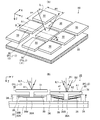
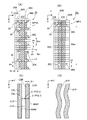
- FIG. 1A is an enlarged perspective view showing a part of the spatial light modulator 28 in FIG. 1
- FIG. 2B is a cross-sectional view taken along the line BB in FIG.
- (A) is a view showing a shot area of a wafer at the time of scanning exposure
- (B) is a view showing a shot area of the wafer at the time of exposure by the step-and-repeat method.
- FIGS. 4A and 4B are partially enlarged plan views showing examples of the phase distribution of the reflected light set by the spatial light modulator, and FIGS. 4A and 4B, respectively. It is a figure which shows intensity distribution of the aerial image corresponding to phase distribution of ().
- FIG. 5 is a partially enlarged plan view showing another example of the phase distribution of reflected light set by the spatial light modulator
- (D), (E), (F) are respectively It is a figure which shows intensity distribution of the aerial image corresponding to the phase distribution of FIG. 5 (A), FIG. 5 (B), and FIG. 5 (C).
- (A) is a partially enlarged plan view showing an example of a phase distribution of reflected light set in the embodiment
- (B) is a partially enlarged plan view showing a phase distribution of reflected light of a comparative example
- (C) is an embodiment of the embodiment.
- FIG. 4D is an enlarged view showing a resist pattern corresponding to a spatial image of the phase distribution
- FIG. 4D is an enlarged view showing a resist pattern of a comparative example.
- (A) is a partial enlarged plan view showing an example of a phase distribution of reflected light set by the spatial light modulator to form an L & S pattern
- (B) is an aerial image corresponding to the phase distribution of FIG. It is a figure which shows intensity distribution. It is a flowchart which shows an example of the exposure operation
- (A) is a figure which shows an example of the relationship between the target shift amount of a predetermined pattern, and an actual shift amount
- (B) is the target shift amount and actual shift amount of a predetermined pattern in a 1st modification.
- (A), (B), (C), (D) is a partial enlarged plan view showing an example of a phase distribution of reflected light set by the spatial light modulator of the first modification.
- (A) is a figure which shows intensity distribution etc. of the aerial image of the phase distribution of FIG. 7 (A)
- (B) is a figure which shows intensity distribution etc. of the aerial image of the phase distribution of the 2nd modification.
- It is a partial enlarged plan view which shows the phase distribution of the reflected light set with the spatial light modulator of a 2nd modification.
- It is a flowchart which shows an example of the manufacturing process of an electronic device.
- FIG. 1 shows a schematic configuration of a maskless exposure apparatus EX according to the present embodiment.
- an exposure apparatus EX includes an exposure light source 2 that emits pulsed light, an illumination optical system ILS that illuminates a surface to be irradiated with exposure illumination light (exposure light) IL from the light source 2, and an illumination light system ILS.
- a spatial light modulator 28 having a large number of mirror elements 30 each having a variable height and arranged in a two-dimensional array on the irradiation surface or a surface in the vicinity thereof, and driving the spatial light modulator 28 And a modulation control unit 48.
- the exposure apparatus EX receives the illumination light IL reflected by the reflective variable uneven pattern (mask pattern having a variable phase distribution) generated by the multiple mirror elements 30, and the uneven pattern (phase) Projection optical system PL for projecting an aerial image (device pattern) formed corresponding to the distribution) onto the surface of wafer W (substrate), wafer stage WST for positioning and moving wafer W, and the operation of the entire apparatus.
- a main control system 40 composed of a computer for overall control and various control systems are provided.
- a Z-axis is set perpendicular to the bottom surface of wafer stage WST (a surface parallel to a guide surface not shown), and Y-axis is set in a direction parallel to the plane of FIG. 1 in a plane perpendicular to the Z-axis.
- the X axis set in the direction perpendicular to the paper surface of FIG.
- the angles around the X axis, the Y axis, and the Z axis are also called angles in the ⁇ x direction, the ⁇ y direction, and the ⁇ z direction, respectively.
- the wafer W is scanned in the Y direction (scanning direction) during exposure.
- an ArF excimer laser light source that emits a pulse of approximately linearly polarized laser light having a wavelength of 193 nm and a pulse width of about 50 ns at a frequency of about 4 to 6 kHz is used.
- a KrF excimer laser light source having a wavelength of 248 nm, a pulsed light emitting diode, or a solid pulse laser light source that generates harmonics of laser light output from a YAG laser or a solid state laser (semiconductor laser, etc.) Can be used.
- the solid-state pulse laser light source can emit laser light with a wavelength of 193 nm (various other wavelengths are possible) and a pulse width of about 1 ns at a frequency of about 1 to 2 MHz.
- a power source unit 42 is connected to the light source 2.
- the main control system 40 supplies a light emission trigger pulse TP instructing the pulse emission timing and the light amount (pulse energy) to the power supply unit 42.
- the power supply unit 42 causes the light source 2 to perform pulse light emission at the instructed timing and light quantity.
- Illumination light IL made up of pulse laser light having a rectangular cross-sectional shape emitted from the light source 2 and a substantially parallel light beam is a beam expander 4 made up of a pair of lenses, and a polarization control optical system 6 that controls the polarization state of the illumination light IL.
- the light is incident on a diffractive optical element (diffractive optical element 10A in FIG. 1) selected from a plurality of diffractive optical elements 10A, 10B and the like in parallel to the Y axis via the mirror 8A.
- the polarization control optical system 6 includes, for example, a half-wave plate that rotates the polarization direction of the illumination light IL, a quarter-wave plate for converting the illumination light IL into circularly polarized light, and the illumination light IL that is randomly polarized (non-polarized light).
- the diffractive optical elements 10 ⁇ / b> A, 10 ⁇ / b> B and the like are fixed to the peripheral portion of the rotating plate 12 at substantially equal angular intervals.
- the main control system 40 controls the angle of the rotating plate 12 via the drive unit 12a, and installs the diffractive optical element selected according to the illumination condition on the optical path of the illumination light IL.
- the illumination light IL diffracted by the selected diffractive optical element is guided to the incident surface of the microlens array 16 by the relay optical system 14 including the lenses 14a and 14b.
- the illumination light IL incident on the microlens array 16 is two-dimensionally divided by a large number of minute lens elements constituting the microlens array 16, and the pupil plane of the illumination optical system ILS that is the rear focal plane of each lens element.
- a secondary light source (surface light source) is formed on (illumination pupil plane IPP).
- the diffractive optical element 10A is for normal illumination
- the diffractive optical element 10B is for small ⁇ illumination that generates illumination light with a small coherence factor ( ⁇ value).
- Diffractive optical elements (not shown) for illumination and annular illumination are also provided.
- a spatial light modulator having an array of a large number of micromirrors each having a variable tilt angle may be used, and a fly-eye lens instead of the microlens array 16 Etc. can also be used.
- Illumination light IL from the secondary light source formed on the illumination pupil plane IPP includes a first relay lens 18, a field stop 20, a mirror 8B that bends the optical path in the -Z direction, a second relay lens 22, a condenser optical system 24, and The light enters the irradiated surface (the surface on which the designed transfer pattern is arranged) parallel to the XY plane via the mirror 8C at an average incident angle ⁇ in the ⁇ x direction.
- the optical axis AXI of the illumination optical system ILS intersects the irradiated surface in the ⁇ x direction at an incident angle ⁇ .
- the incident angle ⁇ is, for example, several deg (°) to several tens deg.
- An illumination optical system ILS is configured including optical members from the beam expander 4 to the condenser optical system 24 and the mirror 8C.
- Illumination light IL from the illumination optical system ILS illuminates a rectangular illumination area 26A elongated in the X direction on the array of a large number of mirror elements 30 of the spatial light modulator 28 with a substantially uniform illuminance distribution.
- a large number of mirror elements 30 are arranged in a rectangular region including the illumination region 26A at a predetermined pitch in the X direction and the Y direction.
- the illumination optical system ILS and the spatial light modulator 28 are supported by a frame (not shown).
- FIG. 2A is an enlarged perspective view showing a part of the reflection surface of the spatial light modulator 28 in FIG. 1, and FIG. 2B is a cross-sectional view taken along the line BB in FIG. 2A.
- a large number of mirror elements 30 are arranged on the reflection surface of the spatial light modulator 28 at pitches (periods) px and py in the X direction and the Y direction, respectively.
- the width of the mirror element 30 in the X direction and the Y direction can be regarded as being approximately equal to the pitches px and py, respectively.
- the mirror element 30 is square and the pitches px and py are equal to each other.
- the mirror element 30 may be rectangular or the like, and the pitches px and py may be different from each other.
- the number J of arrangement of mirror elements 30 in the Y direction (direction corresponding to the scanning direction of the wafer W) is several hundred to several thousand
- the number I of arrangement in the X direction is several times to several tens of times the number of arrangement J. It is.
- the spatial light modulator 28 includes a large number of mirror elements 30 and a base member 32 that supports the mirror elements 30 via flexible (elastic) hinge portions 35 (see FIG. 2B). It has.
- the base member 32 is made of, for example, a flat base 32A made of silicon, the base material 32A formed on the surface a silicon nitride (e.g., Si 3 N 4) between the insulating layer 32B such as Has been.
- support portions 34 are formed on the surface of the base member 32 at a predetermined pitch in the X direction and the Y direction, and a pair of flexible members in the Z direction is formed between the adjacent support portions 34 in the Y direction by elastic deformation.
- the convex part on the back surface side of the mirror element 30 is supported via the two-stage hinge part 35.
- the support portion 34, the hinge portion 35, and the mirror element 30 are integrally formed from, for example, polysilicon.
- a reflective film 31 made of a thin film of metal (for example, aluminum) is formed on the reflective surface (surface) of the mirror element 30 in order to increase the reflectance.
- an electrode 36A is formed on the surface of the base member 32 on the bottom surface side of the mirror element 30, and an electrode 36B is formed on the bottom surface of the hinge portion 35 so as to face the electrode 36A.
- signal lines (not shown) for applying a predetermined voltage between the electrodes 36A and 36B corresponding to each mirror element 30 are provided in a matrix. In this case, in a state where the voltage is not applied between the electrodes 36A and 36B in the power-off state or the power-on state (first state), the position P (i, j ⁇ 1) at which the illumination light IL2 is incident is obtained.
- the reflection surface of the mirror element 30 matches a reference plane A1 that is a plane parallel to the XY plane.
- the mirror element 30 at the position P (i, j) where the illumination light IL1 is incident is shown.
- the reflecting surface of the mirror element 30 coincides with a plane A2 that is parallel to the XY plane and displaced from the reference plane A1 by the distance d1 in the Z direction.
- each mirror element 30 performs electrodes 36A and 36B for each mirror element 30 at the position P (i, j) according to information on the phase distribution (uneven pattern) of the illumination light IL set from the main control system 40. Control the voltage between.
- Each mirror element 30 is set to either its first state or its second state.
- the spatial light modulator 28 having such a minute three-dimensional structure is manufactured using a MEMS (Microelectromechanical Systems) technology as described in Non-Patent Document 1 cited in the background art, for example. Is possible. Since each mirror element 30 of the spatial light modulator 28 only needs to be set to the first state or the second state by translation, it is easy to reduce the size of the mirror element 30 and increase the number of arrangement of the mirror elements 30. It is.
- MEMS Microelectromechanical Systems
- the amount of change in the phase of the illumination light IL reflected by the mirror element 30 is defined as a first phase ⁇ 1.
- the phase ⁇ 1 is 0 °.
- the phase of the illumination light IL reflected by the mirror element 30 is changed in a state (second state) in which the reflecting surface of each mirror element 30 matches the plane A2 displaced from the reference plane A1 by the distance d1. If the amount is the second phase ⁇ 2, the phase ⁇ 2 is 180 ° ( ⁇ (rad)) different from the phase ⁇ 1. That is, the following relationship is established.
- the phase ⁇ 2 is allowed to have an error of about several deg (°) with respect to the following expression.
- a phase without a unit means rad.
- the difference from the amount of change in the phase of the wavefront of the reflected light B2 when it matches A2 is the second phase ⁇ 2.
- the distance d1 is approximately as follows.
- each mirror element 30 of the spatial light modulator 28 is reflected in the first state in which the phase of the incident illumination light IL is changed by 0 ° or reflected, or the phase of the incident illumination light IL is 180 °. It is controlled to the second state where it is changed and reflected.
- the mirror element 30 set in the first state is also referred to as a phase 0 mirror element
- the mirror element 30 set in the second state is also referred to as a phase ⁇ mirror element.
- the main control system 40 supplies information on the phase distribution (uneven pattern) of the illumination light IL set by the spatial light modulator 28 to the modulation controller 48 every time the illumination light IL having a predetermined number of pulses is emitted. .
- the modulation controller 48 controls each mirror element 30 of the spatial light modulator 28 to phase 0 or phase ⁇ .
- An aerial image corresponding to the phase distribution is formed on the surface of the wafer W.
- the illumination light IL reflected by the array of a large number of mirror elements 30 in the illumination area 26A of the spatial light modulator 28 enters the projection optical system PL at an average incident angle ⁇ .
- a projection optical system PL having an optical axis AXW supported by a column (not shown) is non-telecentric on the spatial light modulator 28 (object plane) side and is a telecentric reduction projection optical system on the wafer W (image plane) side. is there.
- the projection optical system PL converts a reduced image of the aerial image corresponding to the phase distribution of the illumination light IL set by the spatial light modulator 28 into an exposure area 26B (an illumination area 26A and an illumination area 26A) in one shot area of the wafer W.
- the projection magnification ⁇ of the projection optical system PL is, for example, about 1/10 to 1/100.
- the resolution Re of the projection optical system PL (twice the pitch or line width of the periodic pattern)
- the resolution limit expressed by is as follows.
- the resolution Re is about 1 to several times the image width ( ⁇ ⁇ py) of the mirror element 30 of the spatial light modulator 28.
- the resolution Re is several tens of nm to several times that.
- the wafer W (substrate) includes, for example, a photoresist (photosensitive material) applied to a surface of a circular flat substrate such as silicon or SOI (silicon on insulator) with a thickness of about several tens to 200 nm. .
- the reflection surfaces of the many mirror elements 30 of the spatial light modulator 28 and the exposure surface of the wafer W are substantially reduced. Can be placed in parallel. Therefore, it is easy to design and manufacture the exposure apparatus. Furthermore, the polarization state of the illumination light IL can be set to an arbitrary state.
- the exposure apparatus EX is a liquid immersion type, as disclosed in, for example, US Patent Application Publication No. 2007/242247, a space between the optical member at the tip of the projection optical system PL and the wafer W is disclosed. A local liquid immersion device for supplying and recovering a liquid (for example, pure water) that transmits the illumination light IL is provided. In the case of the immersion type, since the numerical aperture NA can be larger than 1, the resolution can be further increased.
- a wafer W is sucked and held on the upper surface of a wafer stage WST via a wafer holder (not shown), and the wafer stage WST performs step movement in the X direction and the Y direction on a guide surface (not shown). Move at a constant speed in the direction.
- the position of wafer stage WST in the X and Y directions, the rotation angle in the ⁇ z direction, and the like are formed by laser interferometer 45, and this measurement information is supplied to stage control system 44.
- Stage control system 44 controls the position and speed of wafer stage WST via drive system 46 such as a linear motor based on control information from main control system 40 and measurement information from laser interferometer 45.
- an alignment system (not shown) for detecting the position of the alignment mark on the wafer W is also provided.
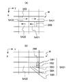
- the wafer W When the wafer W is exposed, as a basic operation, the wafer W is aligned, and then the illumination condition of the illumination optical system ILS is set. In addition, information on the phase distribution corresponding to the pattern exposed to each shot area of the wafer W is supplied from the main control system 40 to the modulation control unit 48. Then, for example, the wafer W is positioned at the scanning start position in order to perform exposure on the shot areas SA21, SA22,... Arranged in a line in the Y direction on the surface of the wafer W shown in FIG. Thereafter, scanning of the wafer W at a constant speed in the + Y direction is started.
- 3A indicates the relative movement direction of the exposure area 26B with respect to the wafer W.
- the main control system 40 supplies information on the relative position of the shot area SA21 of the wafer W to the exposure area 26B to the modulation control section 48, and the modulation control section 48 responds to the relative position by the modulation control section 48.
- the distribution is read, and the read partial phase distribution is set by the spatial light modulator 28.
- the main control system 40 supplies the light emission trigger pulse TP to the power supply unit 42, whereby a target aerial image is exposed in the exposure region 26B on the wafer W according to the position in the Y direction. This operation is repeated every time the wafer W moves by a predetermined amount and until the shot area SA21 crosses the exposure area 26B.
- the main control system 40 causes the modulation control unit 48 to make the shot area SA22 relative to the exposure area 26B while scanning the wafer W in the same direction.
- the position information is supplied and the light emission trigger pulse TP is supplied to the power supply unit 42.
- the wafer stage WST is driven to move the wafer W in the X direction (perpendicular to the scanning direction). In the non-scanning direction).
- the scanning direction of the wafer W with respect to the exposure area 26B indicated by the dotted line is set to the opposite ⁇ Y direction, and information on the relative position of the shot area SA31 and the like with respect to the exposure area 26B is supplied from the main control system 40 to the modulation control unit 48.
- the light emission trigger pulse TP is supplied to the power supply unit 42.
- the illumination condition of the illumination optical system ILS in this case is, for example, a small ⁇ illumination with a ⁇ value of about 0.14, and the polarization direction of the illumination light IL is on the wafer W in the X direction (the longitudinal direction of the line pattern). Is set.
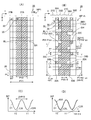
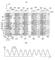
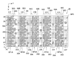
- each mirror element 30 is in a second state (phase ⁇ ) in a rectangular first pattern region 37A including a plurality of columns (for example, four columns or more) and a plurality of rows (for example, 15 rows or more) mirror elements 30 in the X direction.
- a rectangular second pattern region 37B that is adjacent to the first pattern region 37A in the ⁇ Y direction and has substantially the same size as the first pattern region 37A (in FIG. 4A, two columns in the + Y direction appear. ) Is set to a distribution in which each mirror element 30 is in the first state (phase 0).
- the mirror element 30 in the second state (phase ⁇ ) is hatched in FIG. 4A, FIG. 4B described later, and FIGS. 5A to 5C. Yes.
- pattern regions 37A and 37B having a width PY2 in the Y direction are alternately arranged in the Y direction to form a periodic phase distribution.
- the array of mirror elements 30 of phase 0 for two columns arranged adjacent to the first pattern region 37A in the + Y direction is a part of the second pattern region 37B of the next period. is there.
- phase patterns MP1A, MP1B ⁇ for one pitch (one cycle) in the Y direction of the periodic phase distribution, respectively. MP1D etc. are shown.
- the distribution of the intensity INT in the Y direction of the aerial image projected onto, for example, a positive photoresist layer on the surface of the wafer W by the illumination light IL from the phase pattern MP1 in FIG. 4A is the intensity distribution in FIG. As indicated by C1, it is minimum at positions Y1 and Y2 in the Y direction, and the interval between positions Y1 and Y2 is ⁇ ⁇ PY2 ( ⁇ is the projection magnification).
- the intensity distribution C1 is expressed by the center lines C2R and C2L (positions Y1 and Y2) parallel to the X direction conjugate with the boundary lines BR and BL between the pattern area 37A and the pattern area 37B in the ⁇ Y direction in FIG.
- the center of the line pattern formed on the surface of the wafer W is set at an interval ⁇ 1 narrower than the image width of the mirror element 30 (or an interval obtained by adding an integer multiple of the image width and a fraction smaller than the width). Shift in the Y direction.
- the distribution of the intensity INT of the aerial image for forming the line pattern after the shift is in the Y direction with respect to the intensity distribution C1 of the dotted line before the shift, as indicated by the solid line intensity distribution 60A in FIG. It has moved by ⁇ 1. This is the case, for example, when a resist pattern having a shape in which the resist pattern is shifted in the Y direction by an interval ⁇ 1 at a position away from the resist pattern corresponding to the phase pattern MP1 in FIG. Alternatively, it is necessary when the phase pattern MP1 generated by the spatial light modulator 28 is gradually shifted in the Y direction following the movement of the wafer W in the Y direction during the scanning exposure of the wafer W.
- the phase pattern MP1A of the array of mirror elements 30 of the spatial light modulator 28 corresponds to the boundary lines BR and BL of the phase pattern MP1 in FIG. 4A corresponding to ⁇ 1, as shown in FIG. 4B.
- Is substantially equivalent to a phase distribution (target phase distribution) in which the phase becomes ⁇ inside the boundary lines BR1 and BL1 shifted in the Y direction by ⁇ y ( ⁇ 1 / ⁇ ) and becomes phase 0 outside them. I just need it.
- the phase pattern MP1A of FIG. 4B all of the first pattern region 37C corresponding to a portion of the first pattern region 37A of FIG. 4A excluding one row of mirror elements 30 at both ends in the Y direction.
- the mirror element 30 is in phase ⁇ (second state).
- the second pattern region 37D including an array of a plurality of rows (here, two rows) of mirror elements 30 corresponding to a portion excluding one row at both ends in the Y direction in the second pattern region 37B of FIG.
- the inner mirror element 30 is in phase 0 (first state).
- the first pitch P1 that is not resolved in the X direction by the projection optical system PL in the first boundary region 38A composed of one row of mirror elements 30 arranged adjacent to the first pattern region 37C in the + Y direction. Are set to phase 0, and the other mirror elements 30B in the first boundary region 38A are set to phase ⁇ .
- the second pitch P2 that is not resolved in the X direction by the projection optical system PL. are set to phase ⁇ , and the other mirror elements 30C in the second boundary region 38B are set to phase 0.
- the boundary between the boundary regions 38A and 38B is the boundary line BR before the phase pattern is shifted.
- N1 and N2 mirror elements 30 (N1 and N2 are each an integer of 2 or more) are included in the pitches P1 and P2, the following relationship is established.
- P1 N1 ⁇ px (4A)
- P2 N2 ⁇ px (4B)
- the pitch of the phase pattern image of the pitch P1 is ⁇ ⁇ P1.
- the pitches P1 and P2 are set so as not to be resolved by the projection optical system PL, it is only necessary to obtain a condition that the ⁇ first-order diffracted light from the phase pattern does not pass through the projection optical system PL.
- the phase pattern of the pitches P1 and P2 is not resolved by the projection optical system PL, that is, the phases of the pitches P1 and P2.
- the condition that the pattern exceeds the resolution limit of the projection optical system PL is as follows.
- ⁇ ⁇ P1 ⁇ ⁇ N1 ⁇ px ⁇ / NA (5A)
- ⁇ ⁇ P2 ⁇ ⁇ N2 ⁇ px ⁇ / NA (5B)
- the conditions of the integers N1 and N2 are as follows.
- ⁇ ⁇ px the width of the image of the mirror element 30
- a condition for forming a phase pattern MP1A equivalent to a phase distribution having a boundary line BR1 shifted by ⁇ y with respect to the boundary line BR is: Using the width of the boundary regions 38A and 38B in the Y direction (here, the same as the width of the mirror element 30 in the Y direction) py is as follows.
- ⁇ y ⁇ (n1 / N1) + (n2 / N2) ⁇ py (8A)
- the shift amount ⁇ 1 from the position Y1 of the position (image C3R conjugate with the boundary line BR1) where the intensity distribution 60A of FIG. 4D corresponding to the shift amount ⁇ y is minimum is calculated using the projection magnification ⁇ as follows. It becomes like this. However, ⁇ ⁇ py (the width in the Y direction of the image of the mirror element 30) is D.
- ⁇ 1 ⁇ (n1 / N1) + (n2 / N2) ⁇ D (8B)
- at least one of the values of the integers N1, N2 and the integers n1, n2 is changed within a range in which the integers N1, N2 defining the pitches P1, P2 satisfy the expressions (6A) and (6B).
- the shift amount ⁇ y of the boundary line BR1 in the phase distribution equivalent to the phase pattern MP1A, and hence the shift amount ⁇ 1 of the image conjugate with the boundary line BR1 are adjusted.
- the pitch P1 and the pitch P2 are different in principle. That is, when the pitches P1 and P2 are equal to each other, one of the phase 0 mirror element 30A and the phase ⁇ mirror element 30D is omitted by cancellation, and thus one of the boundary regions 38A and 38B is omitted.
- the shift amount ⁇ 1 is 1 nm as follows.
- the ⁇ Y-direction boundary line BL1 of the phase distribution equivalent to the phase pattern MP1A in FIG. 4B has a positive sign on the first pattern region 37C side with respect to the original boundary line BL. It has moved by ⁇ y.
- the phase distribution of the third boundary region 39A composed of one row of mirror elements 30 arranged adjacent to the second pattern region 37D in the + Y direction is the phase distribution of the first boundary region 38A.
- the phase distribution of the fourth boundary region 39B is a distribution obtained by inverting the phase distribution of the second boundary region 38B.
- the boundary between the boundary regions 39A and 39B is the boundary line BL before the phase pattern is shifted.
- a plurality of mirror elements 30B arranged in the X direction with a pitch of 5 px and a width of px are respectively in phase. ⁇ is set, and the other mirror element 30A is set to phase 0.
- a plurality of mirror elements 30C arranged in the X direction at a pitch 4px and a width px are set to phase 0, and the other mirror elements 30D are set to phase ⁇ .
- the intensity distribution 60B of FIG. 5D and the intensity distribution 60C of FIG. 5E obtained by shifting the intensity distribution C1 of the image of the phase pattern MP1 of FIG. 4A by 2 nm, 3 nm, and 4 nm in the Y direction.
- the phase distribution of the array of mirror elements 30 of the spatial light modulator 28 is changed to the phase pattern MP1B of FIG. What is necessary is just to set to phase pattern MP1C and phase pattern MP1D of FIG.5 (C).
- a plurality of mirror elements 30A arranged in the X direction with a pitch of 5 px and a width of 2 px each have a phase 0 (first 1)
- the other mirror element 30B is set to the phase ⁇ (second state)
- the width px at the pitch 2px in the X direction respectively.
- the plurality of mirror elements 30D arranged in the above are set to the phase ⁇
- the other mirror elements 30C are set to the phase 0.
- the phase pattern MP1C includes a plurality of mirror elements 30A arranged at a pitch of 4 px and a width px in the X direction.
- the other mirror element 30B is set to the phase ⁇ , and a plurality of mirror elements 30D arranged in the X direction with a pitch of 5 px and a width of 2 px are set to the phase ⁇ in the second boundary region 38F adjacent thereto.
- the other mirror element 30C is set to phase 0.
- the width px at the pitch 5 px in the X direction is set to the phase ⁇
- the other mirror element 30C is set to the phase 0
- the + Y direction (the first Y
- the shift amount ⁇ 1 is 4 nm from the equation (8B).
- the intensity distribution of the image of phase pattern MP1 in FIG. A phase pattern having an intensity distribution shifted by 1 nm can be formed.
- the wafer W is exposed with the aerial image of the phase pattern MP1A in FIG. 4B, it is obtained from the aerial image of the phase pattern MP1 in FIG. 4A as shown in FIG. 6C.
- Two line patterns 60AP parallel to the X axis are obtained, which are formed of resist patterns having center lines C3R and C3L shifted by ⁇ 1 in the Y direction with respect to the center lines C2R and C2L of the line pattern C1P.
- the center lines C3R and C3L of the line pattern 60AP are conjugate (images of the boundary lines BR1 and BL1) with boundary lines BR1 and BL1 having a phase distribution equivalent to the phase pattern MP1A of FIG. 4B, respectively.
- a plurality of mirror elements 30D arranged in the X direction with a pitch 20 px and a width px, respectively, are set to a phase ⁇ , and the other mirror elements 30C are It is conceivable to set the phase to 0 and set the phase distribution of the boundary region 64B adjacent to the ⁇ Y direction of the first pattern region 37E to a distribution obtained by inverting the distribution of the boundary region 62A.
- the resist pattern obtained by exposing the aerial image of the phase pattern MP2 has a shape that periodically swells in the X direction as shown by the two resist patterns 61P in FIG. It is lowered and is not preferable.
- the shift amount in the Y direction of the obtained line pattern can be set to a very small amount of, for example, about 1/20 or less with respect to the image width D of the mirror element 30.
- a line and space pattern (hereinafter referred to as an L & S pattern) in which line patterns extending in the X direction are arranged on the surface of the wafer W at a pitch that is a non-integer multiple of the width of the image of the mirror element 30 in the Y direction. Shall be formed.
- the illumination condition in this case is also set to small ⁇ illumination with a ⁇ value of about 0.14, for example, and the polarization condition is such that the polarization direction of the illumination light IL is the X direction on the wafer W (longitudinal direction of the line pattern).
- the image width D of the mirror element 30 is 20 nm
- an L & S pattern having a pitch of 78 nm is formed on the wafer W.
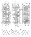
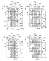
- the array of mirror elements 30 of the spatial light modulator 28 as shown in the partial enlarged plan view of FIG. 7A, 7 columns in the Y direction and a plurality of rows in the X direction (for example, 20 rows or more).
- the phase pattern MP3 including the second, third, fourth, and fifth partial patterns SP2, SP3, SP4, and SP5 including is generated.
- the mirror element 30 in the region adjacent to the first partial pattern SP1 in the ⁇ Y direction is set to phase 0.
- parts corresponding to those in FIGS. 4A to 5C are denoted by the same reference numerals, and detailed description thereof is omitted.
- the first partial pattern SP1 is adjacent to the first pattern region 37E composed of an array of mirror elements 30 with three columns of phase ⁇ in the Y direction and the + Y direction to this region. And a mirror element 30A of phase 0 (first state) having a width px and a mirror element 30B of other phase ⁇ (second state) arranged at a pitch 2px in the X direction.
- One boundary region 38G a mirror element 30D having a width of 2 px (two) arranged adjacent to this region in the + Y direction and having a pitch of 5 px in the X direction, and another mirror element 30C having a phase 0
- a second pattern region 37D comprising an array of two rows of phase 0 mirror elements 30 in the Y direction, which are arranged adjacent to this region in the + Y direction.
- An image of the boundary line BR1 having an equivalent phase distribution (a distribution in which the phase in the ⁇ Y direction of the boundary line BR1 is ⁇ and the phase in the + Y direction is 0) with respect to the image of the boundary line BR of the boundary regions 38G and 38H
- the shift amount ⁇ 1 in the ⁇ Y direction is 2 nm.
- a value ⁇ ⁇ PY3 obtained by multiplying the interval PY3 between the end portion in the ⁇ Y direction of the first pattern region 37E and the boundary line BR1 by the projection magnification ⁇ is 78 nm, and this value ⁇ ⁇ PY1 is formed on the wafer W.
- This is the pitch in the Y direction of the L & S pattern.
- the second partial patterns SP2, SP3, SP4 and SP5 are arranged adjacent to the ⁇ Y direction of the first pattern region 37E or 37C, respectively, and an equivalent phase distribution boundary line image is 4 nm in the ⁇ Y direction.
- boundary regions 64D, 64C, 64E, and 64A for boundary regions 64D, 64C, 64E, and 64A, and the first pattern region 37E or 37C adjacent to each other in the + Y direction, and an image of an equivalent phase distribution boundary line.
- boundary regions 38G and 38I There are boundary regions 38G and 38I, a boundary region 62C, boundary regions 38A and 38D, and boundary regions 38C and 38D for shifting 6 nm, 10 nm, 14 nm, and 18 nm in the ⁇ Y direction.
- the intensity INT of the aerial image of the phase pattern MP3 has an L & S pattern distribution with a uniform pitch of ⁇ ⁇ PY3 of 78 nm as shown in FIG. 7B. Accordingly, when the accuracy of the pitch of the L & S pattern is regarded as one of the shape accuracy, a periodic pattern can be formed with a shape accuracy finer than the width of the image of the mirror element 30 of the spatial light modulator 28.
- step 102 of FIG. 8 a wafer W coated with a photoresist is loaded onto the wafer stage WST of the exposure apparatus EX.
- step 104 the main control system 40 is a spatial light modulator (SLM) 28.
- SLM spatial light modulator
- next step 106 scanning in the Y direction of wafer stage WST is started, and when the tip of the shot area to be exposed on wafer W reaches the exposure area 26B, the main control system sends a modulation control section 48. Is supplied with information on the relative position of the shot area.
- the modulation control unit 48 reads the partial phase distribution of the area (transfer target area) to be transferred to the exposure area 26B from the entire phase distribution data.
- the modulation control unit 48 sets the mirror element 30 in the first state (phase 0) or the second state (phase) in correspondence with the partial phase distribution in units of the mirror element 30 of the spatial light modulator 28. ⁇ ).
- the phase distribution of the transfer target is FIG. 4B
- the mirror element 30 in the first pattern region 37C is set to phase ⁇
- the mirror element 30 in the second pattern region 37D is set to phase 0.
- the modulation control unit 48 determines whether or not the partial phase distribution includes a boundary line (a boundary line between the phase 0 region and the phase ⁇ region) set within the width of the mirror element 30. If it is determined that the boundary line is not included, step 120 is entered. On the other hand, if the boundary line set within the width of the mirror element 30 is included, the process proceeds to step 114. In step 114, the modulation control unit 48 passes the boundary line and the area adjacent to this area (area near the boundary line) (in the example of FIG. 4B, the boundary lines BR1 and BL1 pass).
- the phases of the plurality of mirror elements 30A are set to 0 at the first pitch P1 in the first boundary region 38A (first region), and the phases of the other mirror elements 30B are set. Is set to ⁇ .
- the modulation control unit 48 sets the phase of the plurality of mirror elements 30D to ⁇ at the second pitch P2 in the second boundary region 38B (second region) in FIG.
- the phase of the mirror element 30C is set to zero. If the shift of the boundary line BR with respect to the boundary line BR1 can be performed only by adjusting the phase distribution of the mirror elements 30 in one boundary region, step 116 can be omitted.
- the modulation control unit 48 reverses the phase distribution of the third boundary region 39A (third region) and the fourth boundary region 39B (fourth region) to the distribution of the boundary regions 38A and 38B ( Reverse distribution).
- step 118 can be omitted. Further, when the shift amount of the boundary line BL1 with respect to the boundary line BL is different from the shift amount of the boundary line BR1, the operation of step 118 is executed independently as in step 114 (or steps 114 and 116).
- the main control system 40 supplies the illumination light IL by a predetermined number of pulses from the light source 2 to the spatial light modulator 28 via the illumination optical system ILS. As a result, an aerial image corresponding to the phase distribution set by the spatial light modulator 28 is exposed on the wafer W.
- the operation shifts to step 124, and information on the updated relative position of the shot area to be exposed with respect to the exposure area 26B is supplied from the main control system 40. .
- the modulation control unit 48 shifts the transfer target area in the entire phase distribution in a direction corresponding to the scanning direction. Thereafter, the operation returns to step 108, and in steps 108 to 120, the aerial image corresponding to the partial phase distribution in the shifted transfer target region is exposed on the wafer W. This exposure operation is continued until the scanning exposure is completed in step 122.
- an isolated linear aerial image or an aerial image of the L & S pattern is formed by a maskless method with a positional accuracy or shape accuracy finer than the width of the image of the mirror element 30. be able to. Therefore, various patterns (aerial images) can be formed on the surface of the wafer W with high accuracy.
- the exposure apparatus EX of the present embodiment includes a spatial light modulator 28 and a modulation control unit 48.
- the method for driving the spatial light modulator 28 by the modulation controller 48 is a method for driving the spatial light modulator 28 having an array of a plurality of mirror elements 30 (optical elements) that guide the illumination light IL to the projection optical system PL. is there.
- This drive method is arranged adjacent to the Y direction (first direction) and extends in the X direction (second direction) orthogonal to the Y direction, respectively, among the first boundary region 38A and the second boundary region 38B.
- a plurality of mirror elements 30A arranged at a pitch P1 that is not resolved by the projection optical system PL in the X direction within the first boundary region 38A (exceeds the resolution limit) is set to a phase 0 state (first state).
- the driving method of the spatial light modulator 28 is also a method for generating an exposure pattern.
- the array of the plurality of mirror elements 30 (optical elements) of the spatial light modulator 28 can be regarded as a plurality of sections arranged in a grid, and the first state (phase 0) and the second state
- the arrangement of the plurality of mirror elements 30 (sections) of the spatial light modulator 28 set to (phase ⁇ ) can be regarded as an exposure pattern.
- the plurality of mirror elements 30A arranged at the pitch P1 in the first boundary region 38A are set to phase 0, and arranged at the pitch P2 in the second boundary region 38B.
- the image of the boundary line BR between the boundary regions 38A and 38B is substantially equal to the width of the image of the mirror element 30 in the Y direction based on the equation (8B). Shift with position accuracy finer than D. Therefore, when a pattern is projected onto the wafer W using the spatial light modulator 28, the pattern can be formed with a positional accuracy or shape accuracy that is finer than the width of the image of the mirror element 30.
- the arrangement pitch of the mirror elements 30A and 30D is a pitch that is not resolved by the projection optical system PL, when forming the line pattern on the wafer W, the linearity of the line pattern is maintained and two adjacent ones are adjacent to each other.
- the shift amount of the image of the boundary line BR can be controlled with finer accuracy.
- the exposure apparatus EX is an exposure apparatus that exposes the wafer W (substrate) with illumination light IL (exposure light) via the projection optical system PL, and is disposed on the object plane side of the projection optical system PL.
- a spatial light modulator 28 having an array of a plurality of mirror elements 30 that can be controlled to guide the illumination light IL to the projection optical system PL, and a modulation control unit 48 that drives the plurality of mirror elements 30 of the spatial light modulator 28 ( Control device). Then, the modulation control unit 48 selects the first boundary region among the boundary regions 38A and 38B arranged adjacent to each other in the Y direction according to the aerial image formed on the surface of the wafer W via the projection optical system PL.
- a plurality of mirror elements 30A arranged at a pitch P1 not resolved by the projection optical system PL in the X direction in 38A are set to a state of phase 0, and the other mirror elements 30B are set to a state of phase ⁇ .
- a plurality of mirror elements 30D arranged at a pitch P2 that is not resolved in the X direction in the boundary region 38B by the projection optical system PL are set to the phase ⁇ state, and the other mirror elements 30C are set to the phase 0 state.
- a pattern when a pattern is projected (formed) on the wafer W using the spatial light modulator 28, a pattern (resist pattern or the like) can be formed with a positional accuracy or shape accuracy finer than the width of the image of the mirror element 30.
- step 116 and step 118 may be executed substantially simultaneously. It is also possible to execute step 118 before step 116.
- the boundary line is substantially shifted in the X direction by a finer amount than the width of the mirror element 30 with respect to the boundary line parallel to the Y axis of the array of mirror elements 30 (the region between the mirror elements 30).
- the present embodiment can also be applied to a case where a phase distribution equivalent to a phase distribution in which a phase 0 region and a phase ⁇ region are separated is set.
- the phase of the plurality of mirror elements 30 arranged at a pitch that is not resolved by the projection optical system PL in the two boundary regions adjacent to each other in the X direction in the array of mirror elements 30 is set to 0 or ⁇ . You only have to set it.
- the spatial light modulator 28 since the spatial light modulator 28 has the mirror element 30 (reflection element) as an optical element, the use efficiency of the illumination light IL is high.
- the spatial light modulator 28 instead of the spatial light modulator 28, it is also possible to use a transmissive spatial light modulator that changes the phase of light transmitted by each optical element by a predetermined ⁇ 1 or ( ⁇ 1 + 180 °).
- an optical element an electro-optical element or a liquid crystal cell whose refractive index changes with voltage can be used.
- the wafer W (substrate) is passed through the spatial light modulator 28 having an array of a plurality of mirror elements 30 and the projection optical system PL with illumination light IL (exposure light).
- An exposure method for exposing wherein at least a part of the plurality of mirror elements 30 (mirror elements 30 in the illumination region 26A) is set to a phase 0 or ⁇ state by the driving method of the spatial light modulator 28 described above. , 116, and a step 120 of exposing the wafer W with a plurality of mirror elements 30 set in the phase 0 or ⁇ state with the illumination light IL and the aerial image formed via the projection optical system PL.
- each mirror element 30 of the spatial light modulator 28 is in a third state (a state in which the phase is changed by ⁇ / 2) other than the phase 0 state (first state) and the phase ⁇ state (second state). Etc.) may be set in a plurality of states.
- the illumination light IL from the illumination optical system ILS is incident on the plurality of mirror elements 30 (reflection elements) obliquely at an incident angle ⁇ , and the reflected light from the mirror elements 30 is projected onto the projection optical system PL.
- Incident light intersects the optical axis AXW of the optical system PL. Therefore, since the projection optical system PL is non-telecentric on the object plane side, the entire reflected light from the spatial light modulator 28 can be irradiated onto the wafer W via the projection optical system PL, and the utilization efficiency of the illumination light IL is high. . Furthermore, the polarization state of the illumination light IL set by the polarization control optical system 6 can be accurately reproduced on the surface of the wafer W.
- the mirror element 30 is provided in a rectangular region whose longitudinal direction is the X direction (second direction), and the exposure apparatus EX is configured so that the exposure apparatus EX applies the Y direction orthogonal to the X direction on the image plane of the projection optical system PL ( A wafer stage WST (substrate stage) that moves in the scanning direction corresponding to the first direction), and the modulation control unit 48 forms a pattern formed by the plurality of mirror elements 30 in accordance with the movement of the wafer W by the wafer stage WST. (Phase distribution) is moved in the Y direction. Thereby, the entire surface of the wafer W can be efficiently exposed.
- P2 and the integers n1, n2 defining the number of mirror elements 30A, 30D within one pitch are adjusted so that ⁇ y in the Y direction with respect to the boundary line BR of the boundary regions 38A, 38B It is possible to generate a phase distribution equivalent to a phase distribution in which the phase is ⁇ in the ⁇ Y direction and the phase is 0 in the + Y direction of the boundary line BR1 that is shifted by a distance.
- a dotted line C4T indicates the same vertical axis value as the target shift amount (nm)
- a solid broken line C4R indicates the actual shift amount (nm) with respect to the target shift amount. Therefore, the difference between the broken line C4R and the straight line C4T is the shift amount error er1.
- the error er1 is maximum at 1.6 nm, particularly when the target shift amount is 9 nm.
- the projection is performed so that the actual shift amount of the intensity distribution of the aerial image is as close as possible to the target shift amount.
- the pitches P1, P2 integer N1, N2 of the mirror elements 30A, 30D of phase 0 or ⁇ in two adjacent boundary regions and the mirrors in one pitch
- the number of elements 30A, 30D is changed.
- the phase pattern MP42 having an actual shift amount of 2 nm in FIG.
- the phase distribution of the boundary regions 39J and 39B on the ⁇ Y direction side of the first pattern region 37C is a distribution obtained by inverting the distribution of the boundary regions 38J and 38B.
- the phase pattern MP46 having an actual shift amount of 6 nm in FIG.
- the phase distribution of the boundary regions 39K and 39L on the ⁇ Y direction side of the first pattern region 37C is a distribution obtained by inverting the distribution of the boundary regions 38K and 38L.
- the phase distribution of the boundary regions 39J and 39D on the ⁇ Y direction side of the first pattern region 37C is a distribution obtained by inverting the distribution of the boundary regions 38J and 38D. is there.
- the phase distribution of the boundary regions 39A and 39M on the ⁇ Y direction side of the first pattern region 37C is a distribution obtained by inverting the distribution of the boundary regions 38A and 38M.
- the dotted straight line C5T in FIG. 9B shows the same vertical axis value as the target shift amount (nm), and the solid broken line C5R is shown in FIG. 10 (b) when the shift amounts are 2 nm, 6 nm, 7 nm, and 9 nm.
- the difference between the broken line C5R and the straight line C5T is the shift amount error er2.
- the error er2 is maximum at 0.3 nm when the target shift amount is 2 nm.
- This error er2 is the error shown in FIG. 9A when the values of the integers N1, N2, and n1, n2 are not adjusted. It is considerably smaller than er1. Therefore, according to the first modification, a target pattern can be formed with higher accuracy.
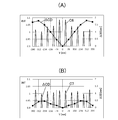
- FIG. 11A shows the result of calculating the intensity distribution of the aerial image of the L & S pattern formed by using the phase pattern MP3 of FIG. 7A of the above embodiment by simulation.
- the horizontal axis is the Y coordinate (nm) of the image plane
- the curve C6 indicates 10 peaks (bright lines) of the intensity INT (relative value) of the L & S pattern
- the broken line ⁇ CD is An error (nm) of a line width CD (critical dimension) with respect to a target value when a threshold value is set for the curve C6 to form a resist pattern is shown. From the curve C6, it can be seen that there is a variation in the peak intensity of the aerial image of the L & S pattern, and from the polygonal line ⁇ CD, it can be seen that a variation in the line width error is about 2 nm.
- the phase distribution of the array of the plurality of mirror elements 30 of the spatial light modulator 28 is used to reduce the variation in the peak intensity (bright line intensity) of the spatial image of the L & S pattern.
- the phase pattern MP5 in FIG. 12 is arranged in the first pattern region 37E (or 37C) in each of the partial patterns SP1A to SP5A at a pitch that is not resolved by the projection optical system PL in the X direction (here, pitch 5px or 6px).
- the plurality of mirror elements 30A thus set are set to phase 0, and are arranged in the second pattern region 37D (or 37F) at a pitch that is not resolved by the projection optical system PL in the X direction (here, the pitch is 6 px or 5 px).
- a plurality of mirror elements 30D are set to a phase ⁇ .
- the phase of the mirror elements 30 other than the mirror element 30A is set to ⁇ in the first pattern area 37E (or 37C), and the phase of the mirror elements 30 other than the mirror element 30D is set in the second pattern area 37D (or 37F). Is set to zero.
- the pitch of the mirror elements 30A in the first pattern region 37E (or 37C) and the pitch of the mirror elements 30D in the second pattern region 37D (or 37F) are the peak levels of the intensity distribution of the aerial image of that portion. May be set to be substantially equal to each other.
- FIG. 11B shows the result of calculating the intensity distribution of the aerial image of the L & S pattern formed using the phase pattern MP5 of FIG. 12 by simulation.
- the horizontal axis is the Y coordinate (nm) of the image plane
- the curve C7 indicates 10 peaks (bright lines) of the intensity INT (relative value) of the L & S pattern
- the broken line ⁇ CD is An error (nm) in line width with respect to a target value when a threshold value is set for the curve C7 to form a resist pattern is shown. From the curve C7, it can be seen that the variation in the peak intensity of the aerial image of the L & S pattern has been reduced, and from the broken line ⁇ CD in FIG. 11B, it can be seen that the variation in the line width error has decreased to about 0.5 nm.
- the method of driving the spatial light modulator 28 by the modulation control unit 48 of the exposure apparatus EX of the second modified example is arranged apart in the Y direction (first direction) and is also in the X direction (second direction).
- a plurality of mirror elements 30A arranged in a pitch (5 px) not resolved by the projection optical system PL in the X direction in the first pattern region 37E It is set to 0 (first state), the other mirror elements 30 in the first pattern area 37E are set to the phase ⁇ , and at least a part (other than the mirror element 30D) of the mirror elements 30 in the second pattern area 37D. Is set to phase 0.
- the first pattern area 37E has the first pattern area 37E.
- the peak level of the corresponding portion of the aerial image can be adjusted. Therefore, the line width and the like of the finally formed line pattern can be optimized.
- the line width of the finally formed line pattern can be controlled with finer precision than the image width of the mirror element 30. .
- the driving method of the spatial light modulator 28 is also a method for generating an exposure pattern.
- the array of the plurality of mirror elements 30 (optical elements) of the spatial light modulator 28 can be regarded as a plurality of sections arranged in a grid, and the first state (phase 0) and the second state
- the arrangement of the plurality of mirror elements 30 (sections) of the spatial light modulator 28 set to (phase ⁇ ) can be regarded as an exposure pattern.
- each shot area (for example, SA21) of the wafer W is divided into a plurality of partial areas SB1 to SB5 in the Y direction, and the partial areas are formed in the exposure area 26B of the projection optical system PL.
- the illumination light IL may be emitted by a predetermined number of pulses, and the partial region SB1 or the like may be exposed with the reflected light from the array of mirror elements 30 of the spatial light modulator 28.
- the wafer W is stepped in the Y direction, and after the next partial area SB2 or the like reaches the exposure area 26B, the partial area SB2 or the like is similarly exposed.
- This method is substantially a step-and-repeat method, but different patterns are exposed on the partial areas SB1 to SB5 and the like.
- the mirror element 30 of the spatial light modulator 28 of the above embodiment is translated to change the phase of the illumination light IL by the first phase or the second phase.
- the tilting is disclosed, for example, as disclosed in US Pat. No. 5,312,513 or US Pat. No. 6,885,493.
- a spatial light modulator having an array of a plurality of mirror elements (reflection elements) having variable angles may be used.
- the first state of the mirror element is a state in which the illumination light from the illumination optical system ILS is guided to the projection optical system PL (a state where the light part is a bright portion).
- the second state of the mirror element is a state where the illumination light from the illumination optical system ILS is not incident on the projection optical system PL (a state where a dark portion is formed).
- a plurality of mirror elements arranged at a finer pitch than the resolution limit of the projection optical system PL in the boundary region extending in the X direction between the first region and the second region for example.
- the state By setting the state to the first state or the second state, it is possible to form a pattern with positional accuracy or shape accuracy finer than the width of the image of the mirror element in the Y direction.
- a spatial light modulator that changes both the tilt angles of the plurality of mirror elements and the phase of the illumination light IL may be used.
- the plurality of mirror elements are translated so as to be translated in the normal direction of the surface on which the plurality of mirror elements are arranged, and the inclination angle of the reflecting surfaces of the plurality of mirror elements with respect to the normal line is changed. To do.
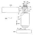
- an exposure apparatus EXA includes a light source (not shown), an illumination optical system ILSA that generates S-polarized illumination light IL in a substantially + Y direction using laser light from the light source, and illumination light IL in the + Z direction.
- the polarizing beam splitter 51 that reflects light
- the quarter-wave plate 52 that converts the illumination light IL from the polarization beam splitter 51 into circularly polarized light
- the circularly polarized illumination light IL are reflected in the ⁇ Z direction or other directions.
- a spatial light modulator 54 having a two-dimensional array of a large number of variable tilt angle mirror elements 56 and a base member 58 that supports these arrays, and a quarter wave plate 52 after being reflected by the mirror element 56.
- a projection optical system PLA that receives the illumination light IL transmitted through the polarization beam splitter 51 and projects an aerial image (pattern) onto the exposure region 26B on the surface of the wafer W.
- the illumination optical system ILSA is an optical system obtained by removing the mirrors 8B and 8C from the illumination optical system ILS in FIG.
- a mirror element 56P in a first state a state in which reflected light is incident on the projection optical system PL
- a mirror element in a second state a state in which the reflected light is not incident on the projection optical system PL.
- a pattern can be formed on the wafer W by a maskless method in combination with 56N.
- the array of mirror elements 56 is arranged at a boundary region extending in the X direction between the first region and the second region, for example, at a finer pitch than the resolution limit of the projection optical system PL.
- a pattern can be formed with a positional accuracy or shape accuracy finer than the width (pitch) of the image of the mirror elements 56 in the Y direction.
- the exposure apparatus EXA of the third modified example since the double-sided telecentric projection optical system PLA can be used, the configuration of the exposure apparatus can be simplified.
- the phase variable spatial light modulator 28 of FIG. 1 can be used as the spatial light modulator 54.
- a normal beam splitter may be used instead of the polarization beam splitter 51, and the 1 ⁇ 4 wavelength plate 52 may be omitted.
- polarized illumination can be used.
- a rod type integrator as an internal reflection type optical integrator may be used.
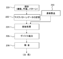
- the electronic device performs step 221 for designing the function / performance of the electronic device, and the mask pattern data based on this design step is set as described above.
- Step 222 for storing in the main control system of the exposure apparatuses EX and EXA of the embodiment, Step 223 for manufacturing a substrate (wafer) as a base material of the device and applying a resist, and the exposure apparatuses EX and EXA (or the exposure method) described above ) Exposing a spatial image of the phase distribution (or intensity distribution generated by the spatial light modulator 54) generated by the spatial light modulator 28 to the substrate (sensitive substrate), developing the exposed substrate, development Substrate processing step 224 including device heating (curing) and etching process, device assembly step (dicing process, Bindings process, including machining processes such as packaging step) 225, and an inspection step 226, and the like.
- This device manufacturing method includes a step of exposing the wafer W using the exposure apparatus (or exposure method) of the above embodiment, and a step of processing the exposed wafer W (step 224). Therefore, an electronic device having a fine circuit pattern can be manufactured with high accuracy. Further, the present invention is not limited to the application to the manufacturing process of a semiconductor device. For example, a manufacturing process such as a liquid crystal display element and a plasma display, an imaging element (CMOS type, CCD, etc.), a micromachine, a MEMS ( (Microelectromechanical systems), thin film magnetic heads, and various devices (electronic devices) such as DNA chips can be widely applied.
- EX, EXA ... exposure apparatus, ILS, ILSA ... illumination optical system, PL, PLA ... projection optical system, W ... wafer, 28 ... spatial light modulator, 30 ... mirror element, 30A, 30C ... phase 0 mirror element, 30B , 30D ... mirror element of phase ⁇ , 37C ... first pattern region, 37D ... second pattern region, 38A ... first boundary region, 38B ... second boundary region, 39A ... third boundary region 39A, 39B ... fourth boundary Area, 48 ... modulation control section
Abstract
Description
図1は、本実施形態に係るマスクレス方式の露光装置EXの概略構成を示す。図1において、露光装置EXは、パルス発光を行う露光用の光源2と、光源2からの露光用の照明光(露光光)ILで被照射面を照明する照明光学系ILSと、ほぼその被照射面又はその近傍の面上に二次元のアレイ状に配列されたそれぞれ高さが可変の微小ミラーである多数のミラー要素30を備えた空間光変調器28と、空間光変調器28を駆動する変調制御部48とを備えている。さらに、露光装置EXは、多数のミラー要素30によって生成された反射型の可変の凹凸パターン(可変の位相分布を持つマスクパターン)で反射された照明光ILを受光して、その凹凸パターン(位相分布)に対応して形成される空間像(デバイスパターン)をウエハW(基板)の表面に投影する投影光学系PLと、ウエハWの位置決め及び移動を行うウエハステージWSTと、装置全体の動作を統括制御するコンピュータよりなる主制御系40と、各種制御系等とを備えている。 An example of an embodiment of the present invention will be described with reference to FIGS.
FIG. 1 shows a schematic configuration of a maskless exposure apparatus EX according to the present embodiment. In FIG. 1, an exposure apparatus EX includes an exposure
光源2から射出された断面形状が矩形でほぼ平行光束のパルスレーザ光よりなる照明光ILは、1対のレンズよりなるビームエキスパンダ4、照明光ILの偏光状態を制御する偏光制御光学系6及びミラー8Aを介して、Y軸に平行に、複数の回折光学素子(diffractive optical element)10A,10B等から選択された回折光学素子(図1では回折光学素子10A)に入射する。偏光制御光学系6は、例えば照明光ILの偏光方向を回転する1/2波長板、照明光ILを円偏光に変換するための1/4波長板、及び照明光ILをランダム偏光(非偏光)に変換するための楔型の複屈折性プリズム等を照明光ILの光路に交換可能に設置可能な光学系である。 In the present embodiment, a
Illumination light IL made up of pulse laser light having a rectangular cross-sectional shape emitted from the
図2(B)において、ベース部材32は、例えばシリコンよりなる平板状の基材32Aと、基材32Aの表面に形成された窒化ケイ素(例えばSi3N4)等の絶縁層32Bとから構成されている。また、ベース部材32の表面にX方向、Y方向に所定ピッチで支持部34が形成され、隣接するY方向の支持部34の間に、弾性変形によってZ方向に可撓性を持つ1対の2段のヒンジ部35を介して、ミラー要素30の裏面側の凸部が支持されている。支持部34、ヒンジ部35、及びミラー要素30は例えばポリシリコンから一体的に形成されている。ミラー要素30の反射面(表面)には、反射率を高めるために金属(例えばアルミニウム等)の薄膜よりなる反射膜31が形成されている。 The spatial
In FIG. 2 (B), the
なお、以下では、単位のない位相はradを意味する。また、位置P(i,j)のミラー要素30の反射面が基準平面A1に合致しているときの点線で示す反射光B1の波面の位相の変化量と、その反射面が間隔d1の平面A2に合致しているときの反射光B2の波面の位相の変化量との差分が第2の位相δ2である。一例として、入射角αをほぼ0°として、ミラー要素30の反射面に入射する照明光IL1の波長をλ(ここではλ=193nm)とすると、間隔d1はほぼ次のようになる。 δ1 = 0 ° (1A), δ2 = 180 ° = π (rad) (1B)
In the following, a phase without a unit means rad. Further, the amount of change in the phase of the wavefront of the reflected light B1 indicated by the dotted line when the reflecting surface of the
図2(A)において、空間光変調器28の各ミラー要素30はそれぞれ入射する照明光ILの位相を0°変化させて反射する第1の状態、又は入射する照明光ILの位相を180°変化させて反射する第2の状態に制御される。以下では、その第1の状態に設定されたミラー要素30を位相0のミラー要素、その第2の状態に設定されたミラー要素30を位相πのミラー要素とも呼ぶこととする。 d1 = λ / 4 (2)
In FIG. 2A, each
図1において、空間光変調器28の照明領域26A内の多数のミラー要素30のアレイで反射された照明光ILは、平均的な入射角αで投影光学系PLに入射する。不図示のコラムに支持された光軸AXWを持つ投影光学系PLは、空間光変調器28(物体面)側に非テレセントリックであり、ウエハW(像面)側にテレセントリックの縮小投影光学系である。投影光学系PLは、空間光変調器28によって設定される照明光ILの位相分布に応じた空間像の縮小像を、ウエハWの1つのショット領域内の露光領域26B(照明領域26Aと光学的に共役な領域)に形成する。投影光学系PLの投影倍率βは例えば1/10~1/100程度である。投影光学系PLの像面側の開口数をNA、照明光ILの波長をλとして、照明条件を通常照明とすると、投影光学系PLの解像度Re(周期的パターンのピッチ又は線幅の2倍で表した解像限界)は、次のようになる。 As an example, the
In FIG. 1, the illumination light IL reflected by the array of a large number of
一例として、解像度Reは、空間光変調器28のミラー要素30の像の幅(β・py)の1倍~数倍程度である。例えば、ミラー要素30の大きさ(配列のピッチ)が数μm程度、投影光学系PLの投影倍率βが1/100程度であれば、解像度Reは数10nm~その数倍程度である。ウエハW(基板)は、例えばシリコン又はSOI(silicon on insulator)等の円形の平板状の基材の表面に、フォトレジスト(感光材料)を数10nm~200nm程度の厚さで塗布したものを含む。 Re = λ / NA (3)
As an example, the resolution Re is about 1 to several times the image width (β · py) of the
また、露光装置EXが液浸型である場合には、例えば米国特許出願公開第2007/242247号明細書に開示されているように、投影光学系PLの先端の光学部材とウエハWとの間に照明光ILを透過する液体(例えば純水)を供給して回収する局所液浸装置が設けられる。液浸型の場合には開口数NAを1より大きくできるため、解像度をさらに高めることができる。 By using the non-telecentric projection optical system PL on the object side as in the present embodiment, the reflection surfaces of the
When the exposure apparatus EX is a liquid immersion type, as disclosed in, for example, US Patent Application Publication No. 2007/242247, a space between the optical member at the tip of the projection optical system PL and the wafer W is disclosed. A local liquid immersion device for supplying and recovering a liquid (for example, pure water) that transmits the illumination light IL is provided. In the case of the immersion type, since the numerical aperture NA can be larger than 1, the resolution can be further increased.
P1=N1・px …(4A), P2=N2・px …(4B)
ここで、投影光学系PLの投影倍率βを用いると、ピッチP1の位相パターンの像のピッチは、β・P1となる。また、ピッチP1,P2は投影光学系PLで解像されないように設定されているため、その位相パターンからの±1次回折光が投影光学系PLを通過しない条件を求めればよい。式(3)の投影光学系PLの解像度Re及び式(4A)、(4B)を用いると、ピッチP1,P2の位相パターンが投影光学系PLで解像されない条件、つまりピッチP1,P2の位相パターンが投影光学系PLの解像限界を超える条件は次のようになる。 Here, assuming that N1 and N2 mirror elements 30 (N1 and N2 are each an integer of 2 or more) are included in the pitches P1 and P2, the following relationship is established.
P1 = N1 · px (4A), P2 = N2 · px (4B)
Here, when the projection magnification β of the projection optical system PL is used, the pitch of the phase pattern image of the pitch P1 is β · P1. Further, since the pitches P1 and P2 are set so as not to be resolved by the projection optical system PL, it is only necessary to obtain a condition that the ± first-order diffracted light from the phase pattern does not pass through the projection optical system PL. Using the resolution Re of the projection optical system PL of the formula (3) and the formulas (4A) and (4B), the phase pattern of the pitches P1 and P2 is not resolved by the projection optical system PL, that is, the phases of the pitches P1 and P2. The condition that the pattern exceeds the resolution limit of the projection optical system PL is as follows.
β・P2=β・N2・px<λ/NA …(5B)
これらの条件から整数N1,N2の条件は次のようになる。ただし、β・px(ミラー要素30の像の幅)をDとおいている。
N1<λ/(NA・D) …(6A), N2<λ/(NA・D) …(6B)
一例として、λ=193nm、NA=1.35(液浸法の適用時)、D=β・px=20(nm)とすると、式(6A)及び(6B)の右辺はほぼ7.15となるため、ピッチP1,P2の位相パターンが投影光学系PLで解像されない条件は、次のように整数N1,N2が7以下であればよい。 β · P1 = β · N1 · px <λ / NA (5A),
β · P2 = β · N2 · px <λ / NA (5B)
From these conditions, the conditions of the integers N1 and N2 are as follows. However, β · px (the width of the image of the mirror element 30) is D.
N1 <λ / (NA · D) (6A), N2 <λ / (NA · D) (6B)
As an example, assuming that λ = 193 nm, NA = 1.35 (when the immersion method is applied), and D = β · px = 20 (nm), the right side of equations (6A) and (6B) is approximately 7.15. Therefore, the condition that the phase pattern of the pitches P1 and P2 is not resolved by the projection optical system PL is that the integers N1 and N2 are 7 or less as follows.
また、図4(B)において、第1境界領域38A内でピッチP1内の位相0のミラー要素30Aの個数をn1(n1はN1より小さい整数)、第2境界領域38B内でピッチP2内の位相πのミラー要素30Dの個数をn2(n2はN2より小さい整数)とすると、境界線BRに対してΔyだけシフトした境界線BR1を持つ位相分布と等価な位相パターンMP1Aを形成する条件は、境界領域38A,38BのY方向の幅(ここではミラー要素30のY方向の幅と同じ)pyを用いて次のようになる。 N1 ≦ 7 (7A), N2 ≦ 7 (7B)
4B, the number of
また、シフト量Δyに対応する図4(D)の強度分布60Aが最小となる位置(境界線BR1と共役な像C3R)の位置Y1からのシフト量δ1は、投影倍率βを用いて次のようになる。ただし、β・py(ミラー要素30の像のY方向の幅)をDとおいている。
δ1={-(n1/N1)+(n2/N2)}D …(8B)
本実施形態では、ピッチP1,P2を規定する整数N1,N2が式(6A)及び(6B)を満たす範囲内で、整数N1,N2及び整数n1,n2の値の少なくとも一つを変更することによって、位相パターンMP1Aと等価な位相分布における境界線BR1のシフト量Δy、ひいては境界線BR1と共役な像のシフト量δ1を調整する。また、光学的近接効果による誤差であるOPE(Optical Proximity Error )等を考慮しないものとすると、2つの境界領域38A,38Bを用いる場合には、原則としてピッチP1とピッチP2とは異なっている。すなわち、ピッチP1,P2が互いに等しいときには、位相0のミラー要素30Aと位相πのミラー要素30Dとの一方が相殺によって省略されるため、境界領域38A,38Bのうちの一方が省略される。 Δy = {− (n1 / N1) + (n2 / N2)} py (8A)
Further, the shift amount δ1 from the position Y1 of the position (image C3R conjugate with the boundary line BR1) where the
δ1 = {− (n1 / N1) + (n2 / N2)} D (8B)
In the present embodiment, at least one of the values of the integers N1, N2 and the integers n1, n2 is changed within a range in which the integers N1, N2 defining the pitches P1, P2 satisfy the expressions (6A) and (6B). Thus, the shift amount Δy of the boundary line BR1 in the phase distribution equivalent to the phase pattern MP1A, and hence the shift amount δ1 of the image conjugate with the boundary line BR1 are adjusted. In addition, assuming that OPE (Optical Proximity Error), which is an error due to the optical proximity effect, is not taken into account, when the two
δ1=(-1/5+1/4)20=1(nm) …(9A)
また、本実施形態では、図4(B)の位相パターンMP1Aと等価な位相分布の-Y方向の境界線BL1は、元の境界線BLに対して第1パターン領域37C側を正の符号としてΔyだけ移動している。このため、位相パターンMP1Aにおいて、第2パターン領域37Dに対して+Y方向に隣接して配置された1列のミラー要素30よりなる第3境界領域39Aの位相分布が第1境界領域38Aの位相分布を反転した分布となり、第3境界領域39Aに対して+Y方向に隣接して配置された(第1パターン領域37Cに対して-Y方向に隣接して配置された)1列のミラー要素30よりなる第4境界領域39Bの位相分布が第2境界領域38Bの位相分布を反転した分布となっている。境界領域39A,39Bの境界が位相パターンをシフトさせる前の境界線BLである。 As an example, when the image width D of the
δ1 = (− 1/5 + 1/4) 20 = 1 (nm) (9A)
In the present embodiment, the −Y-direction boundary line BL1 of the phase distribution equivalent to the phase pattern MP1A in FIG. 4B has a positive sign on the
また、図5(B)の位相パターンMP1Cは、第1パターン領域37Cの+Y方向の第1境界領域38Eで、X方向にピッチ4pxでそれぞれ幅pxで配列された複数のミラー要素30Aを位相0に設定し、他のミラー要素30Bを位相πに設定し、それに隣接する第2境界領域38Fにおいて、X方向にピッチ5pxでそれぞれ幅2pxで配列された複数のミラー要素30Dを位相πに設定し、他のミラー要素30Cを位相0に設定したものである。さらに、第2パターン領域37Dに+Y方向に順次隣接する第3境界領域39E及び第4境界領域39Fの位相分布は、それぞれ境界領域38E及び38Fの分布を反転した分布である。この位相分布は、図4(B)でN1=4,n1=1,N2=5,n2=2とした分布に相当するため、式(8B)からシフト量δ1は3nmとなる。 δ1 = (− 2/5 + 1/2) 20 = 2 (nm) (9B)
5B is a
本実施形態の効果等は以下の通りである。 As described above, according to the present embodiment, an isolated linear aerial image or an aerial image of the L & S pattern is formed by a maskless method with a positional accuracy or shape accuracy finer than the width of the image of the
The effects and the like of this embodiment are as follows.
なお、ステップ116とステップ118とは、実質的に同時に実行することも可能である。また、ステップ118をステップ116よりも先に実行することも可能である。さらに、ミラー要素30のアレイのY軸に平行な境界線(ミラー要素30の間の領域)に対して、実質的にX方向にミラー要素30の幅よりも微細な量だけシフトした境界線で位相0の領域と位相πの領域とが分かれている位相分布と等価な位相分布を設定する場合にも本実施形態が適用できる。この場合には、ミラー要素30のアレイ中で、X方向に隣接する2つの境界領域内で、投影光学系PLに解像されないピッチで配列された複数のミラー要素30の位相を0又はπに設定すればよい。 Therefore, when a pattern is projected (formed) on the wafer W using the spatial
Note that
なお、空間光変調器28の各ミラー要素30は、位相0の状態(第1の状態)及び位相πの状態(第2の状態)以外の第3の状態(位相をπ/2変化させる状態等)等を含む複数の状態に設定可能としてもよい。 According to the exposure method or the exposure apparatus EX, since a pattern (aerial image) can be formed with a finer precision than the width of the image of the
Each
上記の実施形態の空間光変調器28のミラー要素30のアレイにおいて、図4(B)に示すように、境界領域38A及び/又は38B内の位相0又はπのミラー要素30A,30DのピッチP1,P2を規定する整数N1,N2及び1ピッチ内のミラー要素30A,30Dの個数を規定する整数n1,n2を調整することで、境界領域38A,38Bの境界線BRに対してY方向にΔyだけシフトした境界線BR1の-Y方向で位相がπで+Y方向で位相が0となる位相分布と等価な位相分布を生成できる。この際に、例えば光学的近接効果による誤差であるOPE(Optical Proximity Error )等を考慮して、図4(B)の位相パターンMP1Aからの照明光ILによって投影光学系PLを介して像面に形成される強度分布をシミュレーションによって求め、その強度分布の図4(D)の基準となる強度分布C1からのシフト量(実際のシフト量)を求めると、この実際のシフト量が、図9(A)に示すように、整数N1,N2及びn1,n2の値を式(8B)に代入して計算される値(ターゲットシフト量)に対してある誤差を持つことが分かった。図9(A)において、点線の直線C4Tは、ターゲットシフト量(nm)と同じ縦軸の値を示し、実線の折れ線C4Rは、ターゲットシフト量に対する実際のシフト量(nm)を現している。従って、直線C4Tに対する折れ線C4Rの差分がシフト量の誤差er1となる。誤差er1は、特にターゲットシフト量が9nmのときに1.6nmで最大になっている。 In the above embodiment, the following modifications are possible.
In the array of
また、複数のミラー要素の傾斜角と照明光ILの位相との両方を変化させる空間光変調器を用いても良い。この場合、複数のミラー要素は、複数のミラー要素が配列されている面の法線方向に平行移動すると共に、複数のミラー要素の反射面の当該法線に対する傾斜角が変更されるように傾斜する。 When such a tilt angle variable spatial light modulator is used, the first state of the mirror element is a state in which the illumination light from the illumination optical system ILS is guided to the projection optical system PL (a state where the light part is a bright portion). In addition, the second state of the mirror element is a state where the illumination light from the illumination optical system ILS is not incident on the projection optical system PL (a state where a dark portion is formed). Also in this case, in the array of mirror elements, a plurality of mirror elements arranged at a finer pitch than the resolution limit of the projection optical system PL in the boundary region extending in the X direction between the first region and the second region, for example. By setting the state to the first state or the second state, it is possible to form a pattern with positional accuracy or shape accuracy finer than the width of the image of the mirror element in the Y direction.
A spatial light modulator that changes both the tilt angles of the plurality of mirror elements and the phase of the illumination light IL may be used. In this case, the plurality of mirror elements are translated so as to be translated in the normal direction of the surface on which the plurality of mirror elements are arranged, and the inclination angle of the reflecting surfaces of the plurality of mirror elements with respect to the normal line is changed. To do.
なお、照明光ILの利用効率が1/2に低下してもよい場合には、偏光ビームスプリッタ51の代わりに通常のビームスプリッタを使用し、1/4波長板52を省略してもよい。この場合には、偏光照明が使用できる。 In the third modification, the phase variable spatial
When the utilization efficiency of the illumination light IL may be reduced to ½, a normal beam splitter may be used instead of the
また、電子デバイス(又はマイクロデバイス)を製造する場合、電子デバイスは、図14に示すように、電子デバイスの機能・性能設計を行うステップ221、この設計ステップに基づいたマスクのパターンデータを上記の実施形態の露光装置EX,EXAの主制御系に記憶するステップ222、デバイスの基材である基板(ウエハ)を製造してレジストを塗布するステップ223、前述した露光装置EX,EXA(又は露光方法)により空間光変調器28で生成される位相分布(又は空間光変調器54で生成される強度分布)の空間像を基板(感応基板)に露光する工程、露光した基板を現像する工程、現像した基板の加熱(キュア)及びエッチング工程などを含む基板処理ステップ224、デバイス組み立てステップ(ダイシング工程、ボンディング工程、パッケージ工程などの加工プロセスを含む)225、並びに検査ステップ226等を経て製造される。 Further, in place of the
Further, when an electronic device (or micro device) is manufactured, as shown in FIG. 14, the electronic device performs
また、本発明は、半導体デバイスの製造プロセスへの適用に限定されることなく、例えば、液晶表示素子、プラズマディスプレイ等の製造プロセスや、撮像素子(CMOS型、CCD等)、マイクロマシーン、MEMS(Microelectromechanical Systems:微小電気機械システム)、薄膜磁気ヘッド、及びDNAチップ等の各種デバイス(電子デバイス)の製造プロセスにも広く適用できる。 This device manufacturing method includes a step of exposing the wafer W using the exposure apparatus (or exposure method) of the above embodiment, and a step of processing the exposed wafer W (step 224). Therefore, an electronic device having a fine circuit pattern can be manufactured with high accuracy.
Further, the present invention is not limited to the application to the manufacturing process of a semiconductor device. For example, a manufacturing process such as a liquid crystal display element and a plasma display, an imaging element (CMOS type, CCD, etc.), a micromachine, a MEMS ( (Microelectromechanical systems), thin film magnetic heads, and various devices (electronic devices) such as DNA chips can be widely applied.
また、本願に記載した上記公報、各国際公開パンフレット、米国特許、又は米国特許出願公開明細書における開示を援用して本明細書の記載の一部とする。また、明細書、特許請求の範囲、図面、及び要約を含む2012年1月18日付け提出の日本国特許出願第2012-007727号の全ての開示内容は、そっくりそのまま引用して本願に組み込まれている。 In addition, this invention is not limited to the above-mentioned embodiment, A various structure can be taken in the range which does not deviate from the summary of this invention.
In addition, the disclosures in the above-mentioned publications, international publication pamphlets, US patents, or US patent application publication specifications described in the present application are incorporated into the description of this specification. In addition, the entire disclosure of Japanese Patent Application No. 2012-007727 filed on January 18, 2012, including the description, claims, drawings, and abstract, is incorporated herein by reference in its entirety. ing.
Claims (25)
- それぞれ光を投影光学系に導くことが可能な複数の光学要素のアレイを有する空間光変調器の駆動方法であって、
第1方向に隣接して配置されるとともにそれぞれ前記第1方向に交差する第2方向に伸びた第1領域及び第2領域のうち、前記第1領域内で前記第2方向に前記投影光学系で解像されない第1のピッチで配列された複数の前記光学要素を第1の状態に設定し、前記第1領域内の他の前記光学要素を前記第1の状態と異なる第2の状態に設定し、
前記第2領域内で前記第2方向に前記投影光学系で解像されない第2のピッチで配列された複数の前記光学要素を前記第2の状態に設定し、前記第2領域内の他の前記光学要素を前記第1の状態に設定する
ことを特徴とする空間光変調器の駆動方法。 A method of driving a spatial light modulator having an array of a plurality of optical elements each capable of guiding light to a projection optical system,
Of the first and second regions arranged adjacent to each other in the first direction and extending in the second direction intersecting the first direction, the projection optical system in the second direction within the first region. A plurality of the optical elements arranged at a first pitch that are not resolved in the first state are set to a first state, and the other optical elements in the first region are set to a second state different from the first state. Set,
A plurality of the optical elements arranged at a second pitch not resolved by the projection optical system in the second direction in the second region are set to the second state, and other optical elements in the second region are set. A method of driving a spatial light modulator, wherein the optical element is set to the first state. - 複数の前記光学要素はそれぞれ反射面を前記反射面に垂直な方向に移動させて入射する光を反射する反射要素であることを特徴とする請求項1に記載の空間光変調器の駆動方法。 The method of driving a spatial light modulator according to claim 1, wherein each of the plurality of optical elements is a reflection element that reflects incident light by moving a reflection surface in a direction perpendicular to the reflection surface.
- 前記投影光学系を介して像面上に形成されるパターンは、前記第1領域と前記第2領域との境界部に対応する境界パターン部を備え、
前記第1領域内で前記第1のピッチ内の前記第1の状態の光学要素の個数をn1、前記第1のピッチをP1、前記第2領域内で前記第2のピッチ内の前記第2の状態の光学要素の個数をn2、前記第2のピッチをP2として、前記光学要素の個数n1及びn2並びに前記ピッチP1及びP2のうちの少なくとも一つの値を変更して前記境界パターン部の前記第1方向に対応する方向の位置を制御することを特徴とする請求項1又は2に記載の空間光変調器の駆動方法。 The pattern formed on the image plane via the projection optical system includes a boundary pattern portion corresponding to a boundary portion between the first region and the second region,
The number of optical elements in the first state within the first pitch within the first region is n1, the first pitch is P1, and the second within the second region is within the second pitch. The number of optical elements in the state of n2 is set to n2, the second pitch is set to P2, and at least one of the numbers n1 and n2 of the optical elements and the pitches P1 and P2 is changed to change the value of the boundary pattern portion. 3. The method of driving a spatial light modulator according to claim 1, wherein a position in a direction corresponding to the first direction is controlled. - 前記第1のピッチと前記第2のピッチとは互いに異なっており、
前記第1のピッチの幅内の前記光学要素の個数をN1、前記第2のピッチの幅内の前記光学要素の個数をN2、前記光学要素の前記投影光学系による像の前記第1方向に対応する方向の幅をDとして、前記像面における前記境界パターン部の前記第1方向に対応する方向の移動量は
{-(n1/N1)+(n2/N2)}D
であることを特徴とする請求項3に記載の空間光変調器の駆動方法。 The first pitch and the second pitch are different from each other;
The number of the optical elements within the width of the first pitch is N1, the number of the optical elements within the width of the second pitch is N2, and the image of the optical element by the projection optical system in the first direction. The width of the corresponding direction is D, and the amount of movement of the boundary pattern portion in the image plane in the direction corresponding to the first direction is {− (n1 / N1) + (n2 / N2)} D
The method of driving a spatial light modulator according to claim 3, wherein: - 前記投影光学系の結像特性、及び前記像面における前記境界パターン部の前記第1方向に対応する方向の移動量の目標値に応じて、前記ピッチP1及びP2、並びに前記光学要素の個数n1及びn2のうち少なくとも一つを変更することを特徴とする請求項3に記載の空間光変調器の駆動方法。 The pitches P1 and P2 and the number of optical elements n1 according to the imaging characteristics of the projection optical system and the target value of the amount of movement of the boundary pattern portion in the direction corresponding to the first direction on the image plane. And at least one of n2 is changed. 4. The method of driving a spatial light modulator according to claim 3, wherein:
- 前記第1領域に対して前記第2領域と逆方向に隣接する第3領域内で前記第2方向に前記投影光学系で解像されない第3のピッチで配列された複数の前記光学要素を前記第1の状態に設定し、前記第3領域内の他の前記光学要素を前記第2の状態に設定することを特徴とする請求項1~5のいずれか一項に記載の空間光変調器の駆動方法。 A plurality of the optical elements arranged at a third pitch that is not resolved by the projection optical system in the second direction in a third region adjacent to the first region in a direction opposite to the second region. 6. The spatial light modulator according to claim 1, wherein the spatial light modulator is set to a first state and the other optical elements in the third region are set to the second state. Driving method.
- それぞれ光を投影光学系に導くことが可能な複数の光学要素のアレイを有する空間光変調器の駆動方法であって、
第1方向に隣接して又は離れて配置されるとともにそれぞれ前記第1方向に交差する第2方向に伸びた第1領域及び第2領域のうち、前記第1領域内で前記第2方向に前記投影光学系で解像されない第1のピッチで配列された複数の前記光学要素を第1の状態に設定し、前記第1領域内の他の前記光学要素を前記第1の状態と異なる第2の状態に設定し、
前記第2領域内の少なくとも一部の前記光学要素を前記第1の状態に設定する
ことを特徴とする空間光変調器の駆動方法。 A method of driving a spatial light modulator having an array of a plurality of optical elements each capable of guiding light to a projection optical system,
Among the first region and the second region that are arranged adjacent to or apart from the first direction and extend in a second direction that intersects the first direction, respectively, the first region in the first region in the second direction. A plurality of the optical elements arranged at a first pitch that are not resolved by the projection optical system are set in a first state, and the other optical elements in the first region are different from the first state. Set to the state of
A method of driving a spatial light modulator, wherein at least a part of the optical elements in the second region is set to the first state. - 複数の前記光学要素はそれぞれ反射面を前記反射面に垂直な方向に移動させて入射する光を反射する反射要素であることを特徴とする請求項7に記載の空間光変調器の駆動方法。 The method of driving a spatial light modulator according to claim 7, wherein each of the plurality of optical elements is a reflection element that reflects incident light by moving a reflection surface in a direction perpendicular to the reflection surface.
- 前記投影光学系を介して像面上に形成されるパターンは、前記第1領域及び前記第2領域に対応する第1パターン部及び第2パターン部を備え、
前記第1パターン部の光強度のピーク値に応じて、前記第1領域内で前記第1のピッチ内の前記第1の状態の光学要素の個数N1及び前記第1のピッチP1の少なくとも一つの値を変更することを特徴とする請求項7又は8に記載の空間光変調器の駆動方法。 The pattern formed on the image plane via the projection optical system includes a first pattern portion and a second pattern portion corresponding to the first region and the second region,
In accordance with the peak value of the light intensity of the first pattern portion, at least one of the number N1 of optical elements in the first state within the first pitch and the first pitch P1 within the first region. 9. The method of driving a spatial light modulator according to claim 7, wherein the value is changed. - 前記第2領域内で前記第2方向に前記投影光学系で解像されない第2のピッチで配列された複数の前記光学要素を前記第2の状態に設定し、前記第2領域内の他の前記光学要素を前記第1の状態に設定することを特徴とする請求項7~9のいずれか一項に記載の空間光変調器の駆動方法。 A plurality of the optical elements arranged at a second pitch not resolved by the projection optical system in the second direction in the second region are set to the second state, and other optical elements in the second region are set. The method of driving a spatial light modulator according to any one of claims 7 to 9, wherein the optical element is set in the first state.
- 前記光学要素の前記第1の状態は、入射する光の位相を第1の位相だけ変化させて前記投影光学系に導く状態であり、前記第2の状態は、入射する光の位相を前記第1の位相と180°異なる第2の位相だけ変化させて前記投影光学系に導く状態であることを特徴とする請求項1~10のいずれか一項に記載の空間光変調器の駆動方法。 The first state of the optical element is a state in which the phase of incident light is changed by a first phase and led to the projection optical system, and the second state is a state in which the phase of incident light is changed to the first phase. 11. The method of driving a spatial light modulator according to claim 1, wherein the second optical phase is changed by a second phase that is 180 ° different from the first phase and is guided to the projection optical system.
- 複数の前記光学要素はそれぞれ傾斜角が可変の反射要素であり、
前記反射要素の前記第1の状態は、前記反射要素で反射される光を前記投影光学系に入射させる状態であり、前記第2の状態は、前記反射要素で反射される光を前記投影光学系に入射させない状態であることを特徴とする請求項1~10のいずれか一項に記載の空間光変調器の駆動方法。 Each of the plurality of optical elements is a reflective element having a variable inclination angle;
The first state of the reflective element is a state where light reflected by the reflective element is incident on the projection optical system, and the second state is a state where light reflected by the reflective element is incident on the projection optical system. The method of driving a spatial light modulator according to any one of claims 1 to 10, wherein the light is not incident on the system. - 露光光で複数の光学要素のアレイを有する空間光変調器及び投影光学系を介して基板を露光する露光方法において、
請求項1~12のいずれか一項に記載の空間光変調器の駆動方法によって複数の前記光学要素の少なくとも一部を前記第1の状態又は前記第2の状態に設定し、
前記露光光で前記第1の状態又は前記第2の状態に設定された複数の前記光学要素及び前記投影光学系を介して形成される空間像で前記基板を露光する
ことを特徴とする露光方法。 In an exposure method of exposing a substrate with exposure light through a spatial light modulator having an array of a plurality of optical elements and a projection optical system,
A method for driving a spatial light modulator according to any one of claims 1 to 12, wherein at least some of the plurality of optical elements are set to the first state or the second state,
An exposure method comprising exposing the substrate with a spatial image formed through the plurality of optical elements and the projection optical system set in the first state or the second state with the exposure light. . - 照明光学系からの露光光で投影光学系を介して基板を露光する露光装置において、
前記投影光学系の物体面側に配置されて、それぞれ前記露光光を前記投影光学系に導くように制御可能な複数の光学要素のアレイを有する空間光変調器と、
前記空間光変調器の複数の前記光学要素を駆動する制御装置と、を備え、
前記制御装置は、前記基板上に前記投影光学系を介して形成される空間像に応じて、
第1方向に隣接して又は離れて配置されるとともにそれぞれ前記第1方向に交差する第2方向に伸びた第1領域及び第2領域のうち、前記第1領域内で前記第2方向に前記投影光学系で解像されない第1のピッチで配列された複数の前記光学要素を第1の状態に設定し、前記第1領域内の他の前記光学要素を前記第1の状態と異なる第2の状態に設定し、
前記第2領域内の少なくとも一部の前記光学要素を前記第1の状態に設定する
ことを特徴とする露光装置。 In an exposure apparatus that exposes a substrate through a projection optical system with exposure light from an illumination optical system,
A spatial light modulator having an array of a plurality of optical elements arranged on the object plane side of the projection optical system, each of which can be controlled to guide the exposure light to the projection optical system;
A controller for driving the plurality of optical elements of the spatial light modulator,
In accordance with the aerial image formed on the substrate via the projection optical system, the control device
Among the first region and the second region that are arranged adjacent to or apart from the first direction and extend in a second direction that intersects the first direction, respectively, the first region in the first region in the second direction. A plurality of the optical elements arranged at a first pitch that are not resolved by the projection optical system are set in a first state, and the other optical elements in the first region are different from the first state. Set to the state of
An exposure apparatus, wherein at least a part of the optical elements in the second region is set to the first state. - 複数の前記光学要素はそれぞれ反射面を前記反射面に垂直な方向に移動させて入射する光を反射する反射要素であることを特徴とする請求項14に記載の露光装置。 15. The exposure apparatus according to claim 14, wherein each of the plurality of optical elements is a reflecting element that reflects incident light by moving a reflecting surface in a direction perpendicular to the reflecting surface.
- 前記第1領域は前記第1方向に前記第2領域に隣接して配置されており、
前記制御装置は、前記第2領域内で前記第2方向に前記投影光学系で解像されない第2のピッチで配列された複数の前記光学要素を前記第2の状態に設定し、前記第2領域内の他の前記光学要素を前記第1の状態に設定する
ことを特徴とする請求項14又は15に記載の露光装置。 The first region is disposed adjacent to the second region in the first direction;
The control device sets the plurality of optical elements arranged at a second pitch that is not resolved by the projection optical system in the second direction in the second region to the second state, and 16. The exposure apparatus according to claim 14, wherein the other optical element in the region is set to the first state. - 複数の前記光学要素はそれぞれ反射要素であり、
前記照明光学系からの前記露光光は、複数の前記反射要素に斜めに入射し、複数の前記反射要素からの反射光が、前記投影光学系に対して前記投影光学系の光軸に交差するように入射することを特徴とする請求項14~16のいずれか一項に記載の露光装置。 Each of the plurality of optical elements is a reflective element;
The exposure light from the illumination optical system is incident on the plurality of reflection elements obliquely, and the reflection light from the plurality of reflection elements intersects the optical axis of the projection optical system with respect to the projection optical system. The exposure apparatus according to any one of claims 14 to 16, wherein the light is incident as follows. - 前記空間光変調器と前記投影光学系との間に配置されるビームスプリッタを備え、
前記照明光学系からの前記露光光は、前記ビームスプリッタ、前記空間光変調器、及び前記ビームスプリッタを介して前記投影光学系に入射することを特徴とする請求項14~16のいずれか一項に記載の露光装置。 A beam splitter disposed between the spatial light modulator and the projection optical system;
The exposure light from the illumination optical system is incident on the projection optical system via the beam splitter, the spatial light modulator, and the beam splitter. The exposure apparatus described in 1. - 複数の前記光学要素のアレイは第3方向を長手方向とする長方形の領域であり、
前記基板を前記投影光学系の像面で前記第1方向に対応する走査方向に移動する基板ステージを備え、
前記制御装置は、前記基板ステージによる前記基板の移動に応じて、複数の前記光学要素によって形成されるパターンを前記第1方向に移動することを特徴とする請求項14~18のいずれか一項に記載の露光装置。 The array of optical elements is a rectangular region having a third direction as a longitudinal direction,
A substrate stage that moves the substrate in a scanning direction corresponding to the first direction on the image plane of the projection optical system;
The control device according to any one of claims 14 to 18, wherein the control device moves a pattern formed by the plurality of optical elements in the first direction in accordance with the movement of the substrate by the substrate stage. The exposure apparatus described in 1. - 投影光学系を用いて基板を露光するときに用いられ、グリッド状に配列された複数の区画を備える露光用パターンの生成方法であって、
第1方向に隣接して又は離れて配置されるとともにそれぞれ前記第1方向に交差する第2方向に伸びた第1領域及び第2領域に配列された前記複数の区画のうち、前記第1領域内で前記第2方向に前記投影光学系で解像されない第1のピッチで配列された複数の前記区画を第1の状態に設定し、前記第1領域内の他の前記区画を前記第1の状態と異なる第2の状態に設定し、
前記第2領域内の少なくとも一部の前記区画を前記第1の状態に設定する
ことを特徴とする露光用パターンの生成方法。 A method for generating an exposure pattern, which is used when a substrate is exposed using a projection optical system and includes a plurality of sections arranged in a grid,
Among the plurality of sections arranged in the second region and the first region that is arranged adjacent to or apart from the first direction and extends in the second direction that intersects the first direction, the first region A plurality of sections arranged at a first pitch not resolved by the projection optical system in the second direction are set to a first state, and the other sections in the first region are set to the first state. Set to a second state different from the state of
A method for generating an exposure pattern, wherein at least a part of the section in the second region is set to the first state. - 前記第1の状態に設定された複数の前記区画と、前記第2の状態に設定された複数の前記区画とは、前記複数の区画が前記グリッド状に配列される面に垂直な方向の位置が異なることを特徴とする請求項20に記載の露光用パターンの生成方法。 The plurality of sections set in the first state and the plurality of sections set in the second state are positions in a direction perpendicular to the plane in which the plurality of sections are arranged in the grid shape. 21. The method for generating an exposure pattern according to claim 20, wherein:
- 前記第1領域は前記第1方向に前記第2領域に隣接して配置されており、
前記第2領域内で前記第2方向に前記投影光学系で解像されない第2のピッチで配列された複数の前記区画を前記第2の状態に設定し、前記第2領域内の他の前記区画を前記第1の状態に設定する
ことを特徴とする請求項21に記載の露光用パターンの生成方法。 The first region is disposed adjacent to the second region in the first direction;
A plurality of the sections arranged at a second pitch not resolved by the projection optical system in the second direction in the second area are set in the second state, and the other sections in the second area are The method for generating an exposure pattern according to claim 21, wherein the section is set to the first state. - 前記第1の状態は、入射する光の位相を第1の位相だけ変化させて前記投影光学系に導く状態であり、前記第2の状態は、入射する光の位相を前記第1の位相とは異なる第2の位相だけ変化させて前記投影光学系に導く状態であることを特徴とする請求項20~22のいずれか一項に記載の露光用パターンの生成方法。 The first state is a state in which the phase of incident light is changed by the first phase and guided to the projection optical system, and the second state is the phase of incident light as the first phase. The method for generating an exposure pattern according to any one of claims 20 to 22, wherein is a state in which the first phase is changed by a different second phase and is guided to the projection optical system.
- 請求項13に記載の露光方法を用いて基板上に感光層のパターンを形成することと、
前記パターンが形成された前記基板を処理することと、
を含むデバイス製造方法。 Forming a pattern of a photosensitive layer on a substrate using the exposure method according to claim 13;
Processing the substrate on which the pattern is formed;
A device manufacturing method including: - 請求項14~19のいずれか一項に記載の露光装置を用いて基板上に感光層のパターンを形成することと、
前記パターンが形成された前記基板を処理することと、
を含むデバイス製造方法。 Forming a pattern of a photosensitive layer on a substrate using the exposure apparatus according to any one of claims 14 to 19,
Processing the substrate on which the pattern is formed;
A device manufacturing method including:
Priority Applications (5)
| Application Number | Priority Date | Filing Date | Title |
|---|---|---|---|
| JP2013554221A JP6137485B2 (en) | 2012-01-18 | 2012-12-26 | Exposure method and apparatus, and device manufacturing method |
| CN201280071531.9A CN104170054B (en) | 2012-01-18 | 2012-12-26 | The driving method of spatial light modulator, the generation method of exposure pattern and exposure method and device |
| KR1020147022167A KR102123347B1 (en) | 2012-01-18 | 2012-12-26 | Drive method for spatial light modulator, method for generating pattern for exposure, and exposure method and device |
| EP12865561.0A EP2806451B1 (en) | 2012-01-18 | 2012-12-26 | Drive method for spatial light modulator, method for generating pattern for exposure, and exposure method and device |
| US14/331,689 US11119411B2 (en) | 2012-01-18 | 2014-07-15 | Drive method for spatial light modulator, method for generating pattern for exposure, and exposure method and apparatus |
Applications Claiming Priority (2)
| Application Number | Priority Date | Filing Date | Title |
|---|---|---|---|
| JP2012007727 | 2012-01-18 | ||
| JP2012-007727 | 2012-01-18 |
Related Child Applications (1)
| Application Number | Title | Priority Date | Filing Date |
|---|---|---|---|
| US14/331,689 Continuation US11119411B2 (en) | 2012-01-18 | 2014-07-15 | Drive method for spatial light modulator, method for generating pattern for exposure, and exposure method and apparatus |
Publications (1)
| Publication Number | Publication Date |
|---|---|
| WO2013108560A1 true WO2013108560A1 (en) | 2013-07-25 |
Family
ID=48798996
Family Applications (1)
| Application Number | Title | Priority Date | Filing Date |
|---|---|---|---|
| PCT/JP2012/083753 WO2013108560A1 (en) | 2012-01-18 | 2012-12-26 | Drive method for spatial light modulator, method for generating pattern for exposure, and exposure method and device |
Country Status (6)
| Country | Link |
|---|---|
| US (1) | US11119411B2 (en) |
| EP (1) | EP2806451B1 (en) |
| JP (3) | JP6137485B2 (en) |
| KR (1) | KR102123347B1 (en) |
| CN (2) | CN104170054B (en) |
| WO (1) | WO2013108560A1 (en) |
Cited By (1)
| Publication number | Priority date | Publication date | Assignee | Title |
|---|---|---|---|---|
| WO2014104001A1 (en) * | 2012-12-26 | 2014-07-03 | 株式会社ニコン | Spatial light modulator and method for driving same, and exposure method and device |
Families Citing this family (8)
| Publication number | Priority date | Publication date | Assignee | Title |
|---|---|---|---|---|
| TWI684788B (en) * | 2011-06-13 | 2020-02-11 | 日商尼康股份有限公司 | Illumination optical system, exposure apparatus and device manufacturing method |
| CN104170054B (en) * | 2012-01-18 | 2018-11-02 | 株式会社尼康 | The driving method of spatial light modulator, the generation method of exposure pattern and exposure method and device |
| CN105763332B (en) * | 2015-12-31 | 2019-02-22 | 中国工程物理研究院电子工程研究所 | A method of the wavefront feedback control based on multipoint function simulation |
| KR20180092738A (en) * | 2017-02-10 | 2018-08-20 | 한국전자통신연구원 | Apparatus and method for obtaining depth information using digital micro-mirror device |
| EP3598236A4 (en) * | 2017-03-16 | 2021-01-20 | Nikon Corporation | Control device and control method, exposure device and exposure method, device manufacturing method, data generation method, and program |
| WO2019064502A1 (en) * | 2017-09-29 | 2019-04-04 | 株式会社ニコン | Electron beam device and device manufacturing method |
| KR20220122705A (en) | 2020-01-10 | 2022-09-02 | 가부시키가이샤 니콘 | Optical apparatus, exposure apparatus, manufacturing method of flat panel display, and device manufacturing method |
| CN116068860A (en) | 2021-11-04 | 2023-05-05 | 邱俊荣 | Exposure apparatus and exposure method |
Citations (9)
| Publication number | Priority date | Publication date | Assignee | Title |
|---|---|---|---|---|
| US5312513A (en) | 1992-04-03 | 1994-05-17 | Texas Instruments Incorporated | Methods of forming multiple phase light modulators |
| US6312134B1 (en) * | 1996-07-25 | 2001-11-06 | Anvik Corporation | Seamless, maskless lithography system using spatial light modulator |
| WO2002041196A1 (en) * | 2000-11-14 | 2002-05-23 | Ball Semiconductor, Inc. | Digital photolithography system for making smooth diagonal components |
| US6885493B2 (en) | 2001-02-05 | 2005-04-26 | Micronic Lasersystems Ab | Method and a device for reducing hysteresis or imprinting in a movable micro-element |
| JP2005536875A (en) * | 2002-08-24 | 2005-12-02 | マスクレス・リソグラフィー・インコーポレーテッド | Continuous direct write photolithography |
| JP2006128194A (en) * | 2004-10-26 | 2006-05-18 | Canon Inc | Exposing apparatus and device manufacturing method |
| US20070242247A1 (en) | 2004-06-09 | 2007-10-18 | Kenichi Shiraishi | Exposure apparatus and device manufacturing method |
| WO2009060745A1 (en) | 2007-11-06 | 2009-05-14 | Nikon Corporation | Control device, exposure method, and exposure device |
| WO2012043497A1 (en) * | 2010-09-27 | 2012-04-05 | 株式会社ニコン | Method for driving spatial light modulator, method for forming pattern for exposure, exposure method, and exposure apparatus |
Family Cites Families (23)
| Publication number | Priority date | Publication date | Assignee | Title |
|---|---|---|---|---|
| US6271957B1 (en) * | 1998-05-29 | 2001-08-07 | Affymetrix, Inc. | Methods involving direct write optical lithography |
| US6537738B1 (en) | 2000-08-08 | 2003-03-25 | Ball Semiconductor, Inc. | System and method for making smooth diagonal components with a digital photolithography system |
| US6606739B2 (en) | 2000-11-14 | 2003-08-12 | Ball Semiconductor, Inc. | Scaling method for a digital photolithography system |
| US6473237B2 (en) | 2000-11-14 | 2002-10-29 | Ball Semiconductor, Inc. | Point array maskless lithography |
| US7302111B2 (en) * | 2001-09-12 | 2007-11-27 | Micronic Laser Systems A.B. | Graphics engine for high precision lithography |
| JP3881865B2 (en) * | 2001-10-19 | 2007-02-14 | 株式会社 液晶先端技術開発センター | Optical recording apparatus and method, and exposure apparatus and method |
| SE0104238D0 (en) * | 2001-12-14 | 2001-12-14 | Micronic Laser Systems Ab | Method and apparatus for patterning a workpiece |
| KR101098070B1 (en) * | 2003-06-12 | 2011-12-26 | 마이크로닉 마이데이터 아베 | Method for high precision printing of patterns |
| JP2005123586A (en) * | 2003-09-25 | 2005-05-12 | Matsushita Electric Ind Co Ltd | Apparatus and method for projection |
| TW200521477A (en) * | 2003-09-25 | 2005-07-01 | Matsushita Electric Ind Co Ltd | Projector and projection method |
| US7016014B2 (en) * | 2004-02-27 | 2006-03-21 | Asml Netherlands B.V | Lithographic apparatus and device manufacturing method |
| US6963434B1 (en) * | 2004-04-30 | 2005-11-08 | Asml Holding N.V. | System and method for calculating aerial image of a spatial light modulator |
| US7209216B2 (en) * | 2005-03-25 | 2007-04-24 | Asml Netherlands B.V. | Lithographic apparatus and device manufacturing method utilizing dynamic correction for magnification and position in maskless lithography |
| JP2007094116A (en) * | 2005-09-29 | 2007-04-12 | Fujifilm Corp | Frame data creating device, method and drawing device |
| US7440078B2 (en) * | 2005-12-20 | 2008-10-21 | Asml Netherlands B.V. | Lithographic apparatus and device manufacturing method using interferometric and maskless exposure units |
| TWI432908B (en) * | 2006-03-10 | 2014-04-01 | Mapper Lithography Ip Bv | Lithography system and projection method |
| WO2007142350A1 (en) * | 2006-06-09 | 2007-12-13 | Nikon Corporation | Pattern formation method, pattern formation device, exposure method, exposure device, and device manufacturing method |
| US8189172B2 (en) * | 2007-06-14 | 2012-05-29 | Asml Netherlands B.V. | Lithographic apparatus and method |
| JP2009071116A (en) * | 2007-09-14 | 2009-04-02 | Ricoh Co Ltd | Maskless exposure device, and exposure method of maskless exposure device |
| JP2010182934A (en) * | 2009-02-06 | 2010-08-19 | Dainippon Screen Mfg Co Ltd | Drawing apparatus and drawing method |
| US8767270B2 (en) * | 2011-08-24 | 2014-07-01 | Palo Alto Research Center Incorporated | Single-pass imaging apparatus with image data scrolling for improved resolution contrast and exposure extent |
| CN104170054B (en) * | 2012-01-18 | 2018-11-02 | 株式会社尼康 | The driving method of spatial light modulator, the generation method of exposure pattern and exposure method and device |
| US20150227075A1 (en) * | 2014-02-07 | 2015-08-13 | Nikon Corporation | Method for improved cd control on 2-phase digital scanner with no loss to image fidelity |
-
2012
- 2012-12-26 CN CN201280071531.9A patent/CN104170054B/en active Active
- 2012-12-26 KR KR1020147022167A patent/KR102123347B1/en active IP Right Grant
- 2012-12-26 WO PCT/JP2012/083753 patent/WO2013108560A1/en active Application Filing
- 2012-12-26 EP EP12865561.0A patent/EP2806451B1/en active Active
- 2012-12-26 JP JP2013554221A patent/JP6137485B2/en active Active
- 2012-12-26 CN CN201811146185.1A patent/CN109164682B/en active Active
-
2014
- 2014-07-15 US US14/331,689 patent/US11119411B2/en active Active
-
2017
- 2017-05-02 JP JP2017091614A patent/JP6429046B2/en active Active
-
2018
- 2018-11-01 JP JP2018206675A patent/JP6756989B2/en active Active
Patent Citations (9)
| Publication number | Priority date | Publication date | Assignee | Title |
|---|---|---|---|---|
| US5312513A (en) | 1992-04-03 | 1994-05-17 | Texas Instruments Incorporated | Methods of forming multiple phase light modulators |
| US6312134B1 (en) * | 1996-07-25 | 2001-11-06 | Anvik Corporation | Seamless, maskless lithography system using spatial light modulator |
| WO2002041196A1 (en) * | 2000-11-14 | 2002-05-23 | Ball Semiconductor, Inc. | Digital photolithography system for making smooth diagonal components |
| US6885493B2 (en) | 2001-02-05 | 2005-04-26 | Micronic Lasersystems Ab | Method and a device for reducing hysteresis or imprinting in a movable micro-element |
| JP2005536875A (en) * | 2002-08-24 | 2005-12-02 | マスクレス・リソグラフィー・インコーポレーテッド | Continuous direct write photolithography |
| US20070242247A1 (en) | 2004-06-09 | 2007-10-18 | Kenichi Shiraishi | Exposure apparatus and device manufacturing method |
| JP2006128194A (en) * | 2004-10-26 | 2006-05-18 | Canon Inc | Exposing apparatus and device manufacturing method |
| WO2009060745A1 (en) | 2007-11-06 | 2009-05-14 | Nikon Corporation | Control device, exposure method, and exposure device |
| WO2012043497A1 (en) * | 2010-09-27 | 2012-04-05 | 株式会社ニコン | Method for driving spatial light modulator, method for forming pattern for exposure, exposure method, and exposure apparatus |
Non-Patent Citations (2)
| Title |
|---|
| See also references of EP2806451A4 |
| YIJIAN CHEN ET AL.: "Design and fabrication of tilting and piston micromirrors for maskless lithography", PROC. OFSPIE (USA, vol. 5751, 2005, pages 1023 - 1037 |
Cited By (1)
| Publication number | Priority date | Publication date | Assignee | Title |
|---|---|---|---|---|
| WO2014104001A1 (en) * | 2012-12-26 | 2014-07-03 | 株式会社ニコン | Spatial light modulator and method for driving same, and exposure method and device |
Also Published As
| Publication number | Publication date |
|---|---|
| JP6137485B2 (en) | 2017-05-31 |
| CN109164682A (en) | 2019-01-08 |
| JP6756989B2 (en) | 2020-09-16 |
| JPWO2013108560A1 (en) | 2015-05-11 |
| JP2017129888A (en) | 2017-07-27 |
| EP2806451A4 (en) | 2016-05-18 |
| US20150077732A1 (en) | 2015-03-19 |
| US11119411B2 (en) | 2021-09-14 |
| EP2806451A1 (en) | 2014-11-26 |
| EP2806451B1 (en) | 2023-01-25 |
| JP2019015993A (en) | 2019-01-31 |
| CN104170054A (en) | 2014-11-26 |
| CN104170054B (en) | 2018-11-02 |
| KR20140114418A (en) | 2014-09-26 |
| KR102123347B1 (en) | 2020-06-16 |
| JP6429046B2 (en) | 2018-11-28 |
| CN109164682B (en) | 2021-01-15 |
Similar Documents
| Publication | Publication Date | Title |
|---|---|---|
| JP6429046B2 (en) | Exposure method and apparatus, and device manufacturing method | |
| JP6229857B2 (en) | Spatial light modulator, exposure apparatus, and device manufacturing method | |
| JP6198023B2 (en) | Exposure method, exposure apparatus, and device manufacturing method | |
| JP5811362B2 (en) | Exposure pattern generation method, exposure method and apparatus, and device manufacturing method | |
| WO2014104001A1 (en) | Spatial light modulator and method for driving same, and exposure method and device | |
| JP6558529B2 (en) | Spatial light modulator and method of using the same, modulation method, exposure method and apparatus, and device manufacturing method | |
| JP6558528B2 (en) | Spatial light modulator and method of using the same, modulation method, exposure method and apparatus, and device manufacturing method |
Legal Events
| Date | Code | Title | Description |
|---|---|---|---|
| 121 | Ep: the epo has been informed by wipo that ep was designated in this application |
Ref document number: 12865561 Country of ref document: EP Kind code of ref document: A1 |
|
| ENP | Entry into the national phase |
Ref document number: 2013554221 Country of ref document: JP Kind code of ref document: A |
|
| NENP | Non-entry into the national phase |
Ref country code: DE |
|
| ENP | Entry into the national phase |
Ref document number: 20147022167 Country of ref document: KR Kind code of ref document: A |
|
| WWE | Wipo information: entry into national phase |
Ref document number: 2012865561 Country of ref document: EP |