WO2013085255A1 - Light emitting diode with improved current spreading - Google Patents
Light emitting diode with improved current spreading Download PDFInfo
- Publication number
- WO2013085255A1 WO2013085255A1 PCT/KR2012/010436 KR2012010436W WO2013085255A1 WO 2013085255 A1 WO2013085255 A1 WO 2013085255A1 KR 2012010436 W KR2012010436 W KR 2012010436W WO 2013085255 A1 WO2013085255 A1 WO 2013085255A1
- Authority
- WO
- WIPO (PCT)
- Prior art keywords
- light emitting
- pad
- emitting diode
- current distribution
- edge
- Prior art date
- Legal status (The legal status is an assumption and is not a legal conclusion. Google has not performed a legal analysis and makes no representation as to the accuracy of the status listed.)
- Ceased
Links
Images










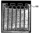
Classifications
-
- H—ELECTRICITY
- H10—SEMICONDUCTOR DEVICES; ELECTRIC SOLID-STATE DEVICES NOT OTHERWISE PROVIDED FOR
- H10H—INORGANIC LIGHT-EMITTING SEMICONDUCTOR DEVICES HAVING POTENTIAL BARRIERS
- H10H20/00—Individual inorganic light-emitting semiconductor devices having potential barriers, e.g. light-emitting diodes [LED]
- H10H20/80—Constructional details
- H10H20/83—Electrodes
- H10H20/831—Electrodes characterised by their shape
Definitions
- Example embodiments of the present invention relate in general to a semiconductor device, and, more specifically, to a light emitting diode.
- a light emitting diode is basically a PN junction diode formed by combining a P-type semiconductor and an N-type semiconductor.
- the electrons transferred to the PN junction are bound to the holes while falling from a conduction band to a valence band.
- the PN junction emits energy corresponding to a difference in height, that is, energy between the conduction band and the valence band. In the process, the energy is emitted in the form of light.
- Such an LED is a semiconductor device that emits light and shows characteristics such as environmental friendliness, low voltage, long lifespan and inexpensiveness.
- the LED was widely applied to a display lamp or display of simple information such as numbers.
- the LED has been used in a variety of fields such display devices, automobile head lamps, projectors, etc.
- LEDs may include horizontal LEDs and vertical LEDs.
- vertical LEDs have excellent current distribution performance compared with horizontal LEDs. That is, horizontal LEDs are formed on a growth substrate for growing an epitaxial layer, and vertical LEDs are positioned on a metal substrate. Therefore, vertical LEDs have an advantage of showing excellent thermal emission performance since they are formed using a metal substrate having high thermal conductivity.
- example embodiments of the present invention are provided to substantially obviate one or more problems due to limitations and disadvantages of the related art.
- Example embodiments of the present invention provide a light emitting diode in which an electric current is uniformly distributed throughout a light emitting region.
- Example embodiments of the present invention also provide a light emitting diode having improved lifespan due to uniform current distribution.
- a light emitting diode in some example embodiments, includes a substrate.
- a semiconductor structure layer including an active layer is disposed on the substrate.
- a pad pattern is disposed on an upper surface of the semiconductor structure layer.
- the pad pattern includes a bonding pad disposed adjacent to a first edge of the upper surface of the semiconductor structure layer, a current distribution pad disposed adjacent to a second edge disposed opposite to the first edge, and extensions configured to electrically connect the bonding pad and the current distribution pad.
- a distance between the bonding pad and the first edge may be the same as a distance between the current distribution pad and the second edge.
- the distance between the bonding pad and the first edge may be in a range of 0.5 to 5% of widths of the light emitting diodes in the same direction.
- the distance between the bonding pad and the first edge may be in a range of 5 to 40 ⁇ m.
- the distance between the current distribution pad and the second edge may be in a range of 0.5 to 5% of the widths of the light emitting diodes in the same direction.
- the distance between the current distribution pad and the second edge may be in a range of 5 to 40 ⁇ m.
- the first and second edges may be first and second sides of the upper surface of the semiconductor structure layer, respectively.
- the bonding pad and the current distribution pad may be disposed at symmetrical positions and formed in the same shape.
- an overlapping region of the current distribution pad and the second edge may have a higher length than an overlapping region of the bonding pad and the first edge.
- the current distribution pad may partially overlap third and fourth edges disposed at both sides of the second edge.
- the bonding pad may have the same area as the current distribution pad.
- the first and second edges may be first and second corners of the upper surface of semiconductor structure layer, respectively.
- the bonding pad and the current distribution pad may be disposed at symmetrical positions and formed in the same shape.
- the current distribution pad may be a first current distribution pad, and a second current distribution pad may be disposed on at least one of third and fourth corners of the upper surface of the semiconductor structure layer.
- the extensions may be disposed adjacent to edges of the upper surface of the semiconductor structure layer. Distance between the extensions and the edges may be in a range of 5 to 40 ⁇ m. The distance between the extensions and the edges may be in a range of 0.5 to 5% of widths of the light emitting diodes in the same direction. The extensions may not lie across a central region of the semiconductor structure layer.
- the bonding pad may not protrude outward relative to the extension adjacent to the bonding pad.
- a distance between the bonding pad and the first edge may be the same as a distance between the extension and the first edge.
- the current distribution pad may not protrude outward relative to the extension adjacent to the current distribution pad.
- a current distribution pad current distribution pad and the second edge may be the same as a distance between the extension and the second edge.
- the light emitting diode includes a substrate.
- a semiconductor structure layer including an active layer is disposed on the substrate.
- a pad pattern is disposed on an upper surface of the semiconductor structure layer.
- the pad pattern includes a bonding pad disposed adjacent to a first edge of the upper surface of the semiconductor structure layer, a current distribution pad disposed spaced apart from the bonding pad, and extensions configured to electrically connect the bonding pad and the current distribution pad. In this case, the bonding pad does not protrude in a direction of the edges relative to the extension adjacent to the bonding pad.
- the distance between the bonding pad and the first edge may be in a range of 0.5 to 5% of widths of the light emitting diodes in the same direction.
- the distance between the bonding pad and the first edge may be the same as the distance between the extension and the first edge.
- the current distribution pad may be disposed adjacent to the other edges other than the first edge of the upper surface of the semiconductor structure layer.
- a distance between the current distribution pad and an edge adjacent to the current distribution pad may be in a range of 0.5 to 5% of the widths of the light emitting diodes in the same direction.
- the extensions may be disposed adjacent to the edges of the upper surface of the semiconductor structure layer. Distances between the extensions and the edges may be in a range of 0.5 to 5% of the widths of the light emitting diodes in the same direction.
- the extensions may not lie across a central region of the semiconductor structure layer. Meanwhile, the current distribution pad may not protrude outward relative to the extension adjacent to the current distribution pad.
- a light emitting diode having improved current spreading performance can be obtained by respectively disposing a bonding pad and a current distribution pad adjacent to facing edges of an upper surface of the semiconductor structure layer. Also, a light emitting diode having improved current spreading performance can be obtained by disposing the bonding pad adjacent to one of the edges of the upper surface of the semiconductor structure layer and arranging the bonding pad so that the bonding pad cannot protrude toward the edge relative to the extension adjacent to the bonding pad.
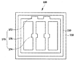
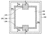
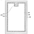
- FIG. 1 is a plane view showing a light emitting diode according to one example embodiment of the present invention.
- FIG. 2 is a cross-sectional view taken along line I-I' shown in FIG. 1.
- FIG. 3 is a plane view showing a light emitting diode according to another example embodiment of the present invention.
- FIG. 4 is a plane view showing a light emitting diode according to still another example embodiment of the present invention.
- FIG. 5 is a plane view showing a light emitting diode according to still another example embodiment of the present invention.
- FIG. 6 is a plane view showing a light emitting diode according to still another example embodiment of the present invention.
- FIG. 7 is a plane view showing a light emitting diode according to still another example embodiment of the present invention.
- FIG. 8 is a cross-sectional view taken along line A-A' shown in FIG. 7.
- FIG. 9 is a plane view showing a light emitting diode according to still another example embodiment of the present invention.
- FIG. 10 is a plane view showing a light emitting diode according to yet another example embodiment of the present invention.
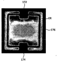
- FIGS. 11A to 11D are images taken while allowing an electric current of 350 mA to flow through light emitting diodes according to Experiment Examples 1 to 4, respectively.
- FIGS. 12A to 12C are plane views showing light emitting diodes according to Experiment Examples 5 to 7, respectively.
- FIGS. 13A to 13C are images taken while allowing an electric current of 350 mA to flow through the light emitting diodes according to Experiment Examples 5 to 7, respectively.
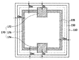
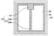
- FIG. 14 is a schematic plane view showing a light emitting diode according to Experiment Example 15.
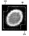
- FIGS. 15A to 15D are images taken while allowing an electric current of 350 mA to flow through light emitting diodes according to Experiment Examples 8 to 11, respectively.
- FIG. 16 is a schematic plane view showing a light emitting diode according to Experiment Example 12.
- FIGS. 17A to 17D are images taken while allowing an electric current of 1,000 mA to flow through light emitting diodes according to Experiment Examples 12 and 13, respectively.
- FIGS. 18A and 18B are images taken while allowing an electric current to flow through light emitting diodes according to Experiment Examples 14 and 15, respectively.
- Example embodiments of the present invention are disclosed herein. However, specific structural and functional details disclosed herein are merely representative for purposes of describing example embodiments of the present invention, however, example embodiments of the present invention may be embodied in many alternate forms and should not be construed as limited to example embodiments of the present invention set forth herein.
- FIG. 1 is a plane view showing a light emitting diode according to one example embodiment of the present invention
- FIG. 2 is a cross-sectional view taken along line I-I' shown in FIG. 1.
- the light emitting diode 100 includes a semiconductor structure layer 150 disposed on a supporting substrate 110.
- a bonding metal layer 120 may be disposed between the supporting substrate 110 and the semiconductor structure layer 150.
- a current spreading inducing layer 130 including a current interrupting pattern 133 and a current transfer pattern 135 may be disposed between the bonding metal layer 120 and the semiconductor structure layer 150.
- a pad pattern 170 including a bonding pad 172, a current distribution pad 174 and extensions 176 configured to electrically connect the bonding pad 172 and the current distribution pad 174 may be disposed on an upper surface of the semiconductor structure layer 150.
- the semiconductor structure layer 150 may include the first-type semiconductor layer 152, a second-type semiconductor layer 156 and an active layer 154 positioned between the first and second-type semiconductor layers 152 and 156.
- the first-type semiconductor layer 152 is a nitride-based semiconductor layer that may be doped with an n-type dopant.
- the first-type semiconductor layer 152 may be a layer in which an In x Al y Ga 1-x-y N (0 ⁇ x ⁇ 1, 0 ⁇ y ⁇ 1, and x+y ⁇ 1) layer is doped with Si as the n-type dopant. More particularly, the first-type semiconductor layer 152 may be a GaN layer doped with Si.
- the first-type semiconductor layer 152 may be provided with a plurality of In x Al y Ga 1-x-y N (0 ⁇ x ⁇ 1, 0 ⁇ y ⁇ 1, and x+y ⁇ 1) layers having different compositions.
- the active layer 154 may be an In x Al y Ga 1-x-y N (0 ⁇ x ⁇ 1, 0 ⁇ y ⁇ 1, and 0 ⁇ x+y ⁇ 1) layer, and have a single quantum well (SQW) structure or multiple quantum well (MQW) structure.
- the active layer 154 may have an SQW structure of an InGaN layer or an AlGaN layer, or a multi-layered structure, that is, an MQW structure, of InGaN/GaN, AlGaN/(In)GaN or InAlGaN/(In)GaN.
- the second-type semiconductor layer 156 may be a nitride-based semiconductor layer, and may be a layer doped with a p-type dopant.
- the second-type semiconductor layer 156 may be a layer in which an In x Al y Ga 1-x-y N (0 ⁇ x ⁇ 1, 0 ⁇ y ⁇ 1, and 0 ⁇ x+y ⁇ 1) layer is doped with Mg or Zn as the p-type dopant. More particularly, the second-type semiconductor layer 156 may be a GaN layer doped with Mg.
- the second-type semiconductor layer 156 may be provided with a plurality of In x Al y Ga 1-x-y N (0 ⁇ x ⁇ 1, 0 ⁇ y ⁇ 1, and 0 ⁇ x+y ⁇ 1) layers having different compositions.
- the supporting substrate 110 may be a semiconductor substrate formed of Si, GaAs, GaP, or InP, or a metal substrate formed of Cu or W.
- the supporting substrate 110 may function to support the semiconductor structure layer 150, and optionally function as an electrode.
- the bonding metal layer 120 is a layer that functions to couple the semiconductor structure layer 150 to the supporting substrate 110, and may be a thermo-compressive bonding layer or a eutectic bonding layer.
- the thermo-compressive bonding layer may be an Au layer/Au layer
- the eutectic bonding layer may be an Au:Sn layer or a Pd:In layer.
- the current spreading inducing layer 130 may include the current interrupting pattern 133 and the current transfer pattern 135.
- the current interrupting pattern 133 is a region that functions to prevent an electric current 180 from flowing in a vertical direction of the bonding pad 172, and may be an insulation pattern.
- the current interrupting pattern 133 may be formed of silicon oxide or silicon nitride.
- the current interrupting pattern 133 may be formed below the bonding pad 172, and also formed below the current distribution pad 174. Further, the current interrupting pattern 133 may be formed below the extensions 176.
- the current transfer pattern 135 is a region that functions to reflect light generated from the active layer 154 while coming in ohmic contact with the semiconductor structure layer 150, particularly, the second-type semiconductor layer 156, and may be a metal pattern.
- the current transfer pattern 135 may be a single metal film or a multiple metal film formed of a material selected from the group consisting of nickel (Ni), platinum (Pt), palladium (Pd), rhodium (Rh), tungsten (W), titanium (Ti), silver (Ag) and gold (Au).
- the bonding pad 172 provided in the pad pattern 170 is disposed adjacent to a first edge of the upper surface of the semiconductor structure layer 150.
- the current distribution pad 174 is disposed apart from the bonding pad 172, and may be disposed in single or plural number.
- the bonding pad 172 is a pad to which an electrical interconnection configured to apply an electric source, such as a conductive wire, is connected during packaging of the light emitting diode 100.
- the current distribution pad 174 is a pad to which no electrical interconnection is connected, and functions to distribute an electric current.
- the first edge may refer to one of sides 150s-1, 150s-2, 150s-3 and 150s-4 of the upper surface of the semiconductor structure layer 150, or one of corners 150c-1, 150c-2, 150c-3 and 150c-4 of the upper surface of the semiconductor structure layer 150.
- the bonding pad 172 may be disposed adjacent to the first side 150s-1 of the upper surface of the semiconductor structure layer 150. More particularly, the bonding pad 172 may be disposed adjacent to a central region of the first side 150s-1.
- the current distribution pad 174 may be disposed adjacent to a second edge positioned opposite to the first edge, particularly, the second side 150s-2 positioned opposite to the first side 150s-1.
- a distance D1 between the bonding pad 172 and the first edge 150s-1 of the upper surface of the semiconductor structure layer 150 may be in a range of 5 to 40 ⁇ m, and may be in a range of 0.5 to 5% of widths 100b of the light emitting diodes 100 in the same direction.
- a distance D2 between the current distribution pad 174 and the second edge 150s-2 of the upper surface of the semiconductor structure layer 150 may be in a range of 5 to 40 ⁇ m, and may be in a range of 0.5 to 5% of the widths 100b of the light emitting diodes 100 in the same direction.
- the bonding pad 172 and the current distribution pad 174 may have substantially the same area, and may be formed in the same shape. Also, the bonding pad 172 and the current distribution pad 174 may be disposed at symmetrical positions.
- Widths 176w of the extensions 176 may be 3 to 10% smaller than a width 172w of the bonding pad 172 and a width 174w of the current distribution pad 174.
- the extensions 176 may be disposed adjacent to the edges of the upper surface of the semiconductor structure layer 150. That is, the extensions 176 may be disposed along the edges of the upper surface of the semiconductor structure layer 150. More particularly, distances De1, De2, De3, De4, De5, De6, De7 and De8 between the extensions 176 and the edges 150s-1, 150s-3, 150s-2, 150s-4, 150c-1, 150c-3, 150c-2 and 150c-4 of the upper surface of the semiconductor structure layer 150 may be in a range of 5 to 40 ⁇ m. In this case, these distances may be in a range of 0.5 to 5% of widths 100a, 100b, 100c and 100d of the light emitting diodes 100 in the same direction.
- the bonding pad 172 may not protrude to an outside direction relative to the extension 176 connected to the bonding pad 172. That is, the distance D1 between the bonding pad 172 and the first edge 150s-1 of the upper surface of the semiconductor structure layer 150 may be substantially the same as a distance De1 between the extension 176 and the first edge 150s-1 of the supper surface of the semiconductor structure layer 150. Also, the current distribution pad 174 may not protrude to an outside direction relative to the extension 176 connected to the current distribution pad 174.
- the distance D2 between the current distribution pad 174 and the second edge 150s-2 of the upper surface of the semiconductor structure layer 150 may be substantially the same as a distance De3 between the extension 176 and the first edge 150s-2 of the upper surface of the semiconductor structure layer 150.
- the pad pattern 170 may not include extensions other than the extension 176, for example, extensions that do not lie across the central region of the upper surface of the semiconductor structure layer 150. That is, all the extensions provided in the pad pattern 170 may be disposed adjacent to the edges of the upper surface of the semiconductor structure layer 150, or disposed along the edges of the upper surface of the semiconductor structure layer 150, as described above.
- the semiconductor structure layer 150 is formed by sequentially stacking the first-type semiconductor layer 152, the active layer 154 and the second-type semiconductor layer 156 on a growth substrate (not shown). Thereafter, the current spreading inducing layer 130 and the bonding metal layer 120 are formed on the second-type semiconductor layer 156, and the supporting substrate 110 is then attached to the bonding metal layer 120. Then, the light emitting diode 100 may be manufactured by removing the growth substrate using a lift-off method such as a laser lift-off (LLO) method or a chemical lift-off (CLO) method, followed by forming the pad pattern 170 on the first-type semiconductor layer 152 that is exposed by removal of the growth substrate.
- the pad pattern 170 may be an Al layer, a Pt layer, a Ni layer, an Au layer, or a composite layer thereof.
- FIG. 3 is a plane view showing a light emitting diode according to another example embodiment of the present invention.
- the light emitting diode according to this example embodiment has a configuration similar to the light emitting diode described with reference to FIGS. 1 and 2, except for the configurations to be described below.
- a pad pattern 170 includes a bonding pad 172 disposed adjacent to a first edge of an upper surface of a semiconductor structure layer 150, and at least one current distribution pad 174 spaced apart from the bonding pad 172.
- the pad pattern 170 may further include extensions 176 configured to electrically connect the bonding pad 172 and the current distribution pad 174.
- the first edge may be a first side 150s-1 of the upper surface of the semiconductor structure layer 150. That is, the bonding pad 172 may be disposed adjacent to the first side 150s-1 of the upper surface of the semiconductor structure layer 150. More particularly, the bonding pad 172 may be disposed adjacent to a central region of the first side 150s-1.
- the current distribution pad 174 may be disposed adjacent to a second edge positioned opposite to the first edge, particularly, a second side 150s-2. Unlike the example embodiment described with reference to FIG. 1, however, the current distribution pad 174 may be configured so that an overlapping region of the current distribution pad 174 and the second edge, particularly, the second side 150s-2, can have a higher length than an overlapping region of the bonding pad 172 and the first edge, particularly, the first side 150s-1. In addition, the current distribution pad 174 may extend to partially overlap third and fourth edges disposed at both sides of the second edge, particularly, third and fourth sides 150s-3 and 150s-4. In this case, widths 174w1 and 174w2 of the current distribution pad 174 may be higher than a width 176w of the extension 176. Meanwhile, the current distribution pad 174 may have substantially the same area as the bonding pad 172.
- FIG. 4 is a plane view showing a light emitting diode according to still another example embodiment of the present invention.
- the light emitting diode according to this example embodiment has a configuration similar to the light emitting diode described with reference to FIGS. 1 and 2, except for the configurations to be described below.
- a pad pattern 170 includes a bonding pad 172 disposed adjacent to a first edge of an upper surface of a semiconductor structure layer 150, and at least one current distribution pad 174 spaced apart from the bonding pad 172.
- the pad pattern 170 may further include extensions 176 configured to electrically connect the bonding pad 172 and the current distribution pad 174.
- the first edge may be a first corner 150c-1 of the upper surface of the semiconductor structure layer 150. That is, the bonding pad 172 may be disposed adjacent to a first corner 150c-1 of the upper surface of the semiconductor structure layer 150. Meanwhile, the current distribution pad 174 may be disposed adjacent to a second edge positioned opposite to the first edge, particularly, a second corner 150s-2.
- the bonding pad 172 and the current distribution pad 174 may have substantially the same area, and may be formed in the same shape. Also, the bonding pad 172 and the current distribution pad 174 may disposed at symmetrical positions.
- FIG. 5 is a plane view showing a light emitting diode according to still another example embodiment of the present invention.
- the light emitting diode according to this example embodiment has a configuration similar to the light emitting diode described with reference to FIGS. 1 and 2, except for the configurations to be described below.
- a pad pattern 170 includes a bonding pad 172 disposed adjacent to a first edge of an upper surface of a semiconductor structure layer 150, and at least one current distribution pad 174 spaced apart from the bonding pad 172.
- the pad pattern 170 may further include extensions 176 configured to electrically connect the bonding pad 172 and the current distribution pad 174.
- the first edge may be a first corner 150c-1 of the upper surface of the semiconductor structure layer 150. That is, the bonding pad 172 may be disposed adjacent to the first corner 150c-1 of the upper surface of the semiconductor structure layer 150.
- the current distribution pad 174 may include a first current distribution pad 174a disposed adjacent to a second edge positioned opposite to the first edge, particularly, a second corner 150s-2, and second and third current distribution pads 174b and 174c disposed respectively at the other corners 150c-3 and 150c-4 of the upper surface of the semiconductor structure layer 150.
- the bonding pad 172 and the first and third current distribution pads 174a, 174b and 174c may be formed in the same shape, and the bonding pad 172 may have substantially the same area as the sum of areas of the first and third current distribution pads 174a, 174b and 174c.
- FIG. 6 is a plane view showing a light emitting diode according to still another example embodiment of the present invention.
- the light emitting diode according to this example embodiment has a configuration similar to the light emitting diode described with reference to FIGS. 1 and 2, except for the configurations to be described below.
- a ratio of the width 100a of the light emitting diode in the first direction and the width 100b of the light emitting diode in the second direction is close to 1:1, whereas, the light emitting diode as shown in FIG. 6 may be formed to have a higher width 100b in the second direction than a width 100a in the first direction.
- a ratio of the width 100a in the first direction and the width 100b in the second direction may be in a range of approximately 1:1.5 to 1:2.
- FIG. 7 is a plane view showing a light emitting diode according to still another example embodiment of the present invention.
- FIG. 8 is a cross-sectional view taken along line A-A' as shown in FIG. 7.
- a light emitting diode 100 may include a supporting substrate 110, a bonding metal layer 120, a current spreading inducing layer 130, a semiconductor structure layer 150, a passivation layer 160 and a pad pattern 170.
- the pad pattern 170 may include a bonding pad 172, a current distribution pad 174, and extensions 176 configured to electrically connect the bonding pad 172 and the current distribution pad 174.
- the supporting substrate 110 may be a substrate that functions to support the semiconductor structure layer 150, for example, a conductive substrate. Also, the supporting substrate 110 may function to apply an electric source to the light emitting diode 100, particularly, the semiconductor structure layer 150, that is, may act as an electrode of the light emitting diode 100.
- the bonding metal layer 120 is interposed between the supporting substrate 110 and a current spreading inducing layer 130 (or a semiconductor structure layer 150) positioned on the supporting substrate 110, and thus functions to couple the supporting substrate 110 and the current spreading inducing layer 130.
- the current spreading inducing layer 130 may include a current interrupting pattern 133 and a current transfer pattern 135.
- the current interrupting pattern 133 may include an open region, and may be formed in a shape in which the current transfer pattern 135 is filled in the open region of the current interrupting pattern 133.
- the current interrupting pattern 133 functions to prevent an electric current 180 supplied from the bonding pad 172, the current distribution pad 174 and the extension 176 from flowing in a vertical direction of the pad pattern 170, thereby allowing the electric current 180 to uniformly flow in the semiconductor structure layer 150, preferably, throughout the active layer 154. That is, the current interrupting pattern 133 functions to sufficiently distribute the electric current 180 supplied to the semiconductor structure layer 150 in the first-type semiconductor layer 152 of the semiconductor structure layer 150 so as to supply the electric current 180 to the active layer 154 provided below the first-type semiconductor layer 152. Also, the current interrupting pattern 133 may function to give information on an etching end point so as to form the semiconductor structure layer 150 during manufacture of the light emitting diode 100.
- the current interrupting pattern 133 may be formed of an insulating material, and may be composed of a silicon oxide film or a silicon nitride film.
- the current transfer pattern 135 may include a material that comes in ohmic contact with the second-type semiconductor layer 156, and reflect light emitted from the active layer 154.
- the current transfer pattern 135 may be referred to as an ohmic reflective metal pattern.
- the current transfer pattern 135 may be formed of a material such as nickel (Ni), platinum (Pt), palladium (Pd), rhodium (Rh), tungsten (W), titanium (Ti), silver (Ag) or gold (Au), which may come in ohmic contact with the P-type semiconductor.
- the bonding metal layer 120 may function to maintain the reflectivity of the current transfer pattern 135 by preventing metal elements from being distributed from the supporting substrate 110 to the current transfer pattern 135.
- a Schottky barrier metal layer (not shown) may be disposed between the bonding metal layer 120 and the current interrupting pattern 133.
- the semiconductor structure layer 150 may include a first-type semiconductor layer 152, an active layer 154 and a second-type semiconductor layer 156.
- the second-type semiconductor layer 156 may be formed on the current spreading inducing layer 130
- the active layer 154 may be formed on the second-type semiconductor layer 156
- the first-type semiconductor layer 152 may be formed on the active layer 154.
- the semiconductor structure layer 150 may further include a superlattice layer (not shown) or an electron blocking layer (not shown). Layers other than the active layer 154 may be omitted in the semiconductor structure layer 150.
- the first-type semiconductor layer 152 may be a III-N-based compound semiconductor doped with first-type impurities, for example, N-type impurities, for example, an (Al, Ga, In) N-based Group III nitride semiconductor layer.
- the first-type semiconductor layer 152 may be a GaN layer doped with N-type impurities, that is, an N-GaN layer.
- the first-type semiconductor layer 152 may have a single-layered or multi-layered structure. For example, when the first-typesemiconductor layer 152 is formed in a multi-layered structure, the first-type semiconductor layer 152 may have a superlattice structure.
- the active layer 154 may be composed of a III-N-based compound semiconductor, for example, an (Al, Ga, In) N semiconductor layer.
- the active layer 154 may be formed of a single layer or multiple layers, and thus may emit light of predetermined wavelengths.
- the active layer 154 may have an SQW structure including one well layer (not shown), and may have an MQW structure in which well layers (not shown) and barrier layers (not shown) are alternately stacked with each other. In this case, one or both of the well layer (not shown) or barrier layer (not shown) may be formed with a superlattice structure.
- the second-type semiconductor layer 156 may be a III-N-based compound semiconductor doped with second-type impurities, for example, P-type impurities, for example, an (Al, In, Ga) N-based Group III nitride semiconductor.
- the second-type semiconductor layer 156 may be a GaN layer doped with P-type impurities, that is, a P-GaN layer.
- the second-type semiconductor layer 156 may be formed with a single-layered or multiple-layered structure.
- the second-type semiconductor layer 156 may be formed with a superlattice structure.
- the superlattice layer may be provided between the first type semiconductor layer 152 and the active layer 154, and may have a structure including layers formed by stacking a plurality of III-N-based compound semiconductors, for example, (Al, Ga, In) N semiconductor layers, for example, repeatedly stacking InN layers and InGaN layers.
- the superlattice layer (not shown) is formed prior to formation of the active layer 154 to prevent dislocations or defects from being transferred to the active layer 154.
- the superlattice layer (not shown) may function to reduce formation of the dislocations or defects of the active layer 154 and maintain excellent crystallinity of the active layer 154.
- the electron blocking layer may be provided between the active layer 154 and the second-type semiconductor layer 156.
- an electron blocking layer may be provided to enhance recombination efficiency of electrons and holes and formed of a material having a relatively wide band gap.
- the electron blocking layer may be formed from an (Al, In, Ga) N-based Group III nitride semiconductor, and made of a P-AlGaN layer doped with Mg.
- the passivation layer 160 may be formed on one surface of the supporting substrate 110 including the semiconductor structure layer 150.
- the passivation layer 160 may function to protect the semiconductor structure layer 150 by covering lateral surfaces as well as one surface of the semiconductor structure layer 150 to prevent the semiconductor structure layer 150 from being exposed to the outside.
- the passivation layer 160 may be made of an insulation film such as a silicon oxide film or a silicon nitride film. Meanwhile, the passivation layer 160 may include an opening 162 configured to expose a certain region of the first conductive semiconductor layer 152.
- the pad pattern 170 may be formed on the passivation layer 160.
- FIG. 8 shows that the pad pattern 170 is formed on the passivation layer 160.
- the pad pattern 170 may be provided between the semiconductor structure layer 150 and the passivation layer 160, that is, may be provided so that the passivation layer 160 can cover the pad pattern 170.
- the passivation layer 160 may have an opening configured to open the bonding pad 172 of the pad pattern 170.
- the bonding pad 172 of the pad pattern 170 may be formed on a certain region of the passivation layer 160, preferably one edge of a surface of the semiconductor structure layer 150.
- the bonding pad 172 may be connected with an external device or an external electric source through a wire (not shown). That is, the light emitting diode 100, particularly, the semiconductor structure layer 150, according to one example embodiment of the present invention is connected to an external electric source through the bonding pad 172.
- the current interrupting pattern 133 may be positioned just under the bonding pad 172.
- the bonding pad 172 may have a smaller size than the current interrupting pattern 133. That is, the bonding pad 172 may be provided so that a width of the bonding pad 172 can be smaller than that of the current interrupting pattern 133.
- the current distribution pad 174 of the pad pattern 170 is formed in plural number on a certain region of the passivation layer 160.
- the current distribution pad 174 may be provided to be spaced apart from the bonding pad 172.
- the current distribution pad 174 may be formed on one edge of the surface of the semiconductor structure layer 150 other than the one edge of the surface of the semiconductor structure layer 150 on which the bonding pad 172 is positioned. That is, when the bonding pad 172 is positioned on one edge of the surface of the semiconductor structure layer 150 as shown in FIG. 7, the current distribution pad 174 may be formed on the other edge of the surface of the semiconductor structure layer 150 that is positioned opposite the one edge on which the bonding pad 172 is positioned.
- the current interrupting pattern 133 may be positioned just under the current distribution pad 174. Therefore, the current interrupting pattern 133 may be provided so that an electric current injected from the current distribution pad 174 to the semiconductor structure layer 150 cannot focus in a vertical direction of the current distribution pad 174 but can be spread within the semiconductor structure layer 150.
- the current distribution pad 174 may have a size identical to or smaller than that of the bonding pad 172.
- the current distribution pad 174 is formed to a wider width than the extension 176.
- the extensions 176 of the pad pattern 170 may be formed on the semiconductor structure layer 150.
- the extensions 176 may be connected to the bonding pad 172, and may be provided to be uniformly distributed on the semiconductor structure layer 150. That is, the extensions 176 may be arranged along the edges on the surface of the semiconductor structure layer 150 surface, and arranged across the central region.
- the extensions 176 are connected to the bonding pad 172 to uniformly distribute an electric source supplied from the outside in the semiconductor structure layer 150, and thus function to inject the electric source into the semiconductor structure layer 150.
- the extensions 176 function to electrically connect the bonding pad 172 and the current distribution pad 174.
- the extensions 176 may be provided in a shape in which the current interrupting pattern 130 is positioned just under the extensions 17.
- the light emitting diode 100 includes a pad pattern 170, which includes the bonding pad 172, the current distribution pad 174 and the extensions 176, all of which are formed on the semiconductor structure layer 150.
- a pad pattern 170 which includes the bonding pad 172, the current distribution pad 174 and the extensions 176, all of which are formed on the semiconductor structure layer 150.
- FIG. 9 is a plane view showing a light emitting diode according to still another example embodiment of the present invention.
- the light emitting diode 100 is different from the light emitting diode 100 described with reference to FIGS. 7 and 8 in that the current distribution pad 174 may be provided on edges other than the one edge of the surface of the semiconductor structure layer 150. That is, the current distribution pad 174 may be disposed on another edge on which the bonding pad 172 is provided among the edges of the semiconductor structure layer 150.
- FIG. 10 is a plane view showing a light emitting diode according to yet another example embodiment of the present invention.
- the light emitting diode 100 according to this example embodiment is different from the light emitting diode 100 described with reference to FIGS. 7 and 8 in that the current distribution pad 174 may be provided on a central region of the surface of the semiconductor structure layer 150. That is, the light emitting diode 100 according to this example embodiment may have a structure in which the current distribution pad 174 is disposed on a certain region on the surface of the semiconductor structure layer 150 other than the edges of the semiconductor structure layer 150.
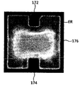
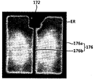
- FIGS. 11A to 11D are images taken while applying an electric current of 350 mA to the light emitting diodes according to Experiment Examples 1 to 4, respectively.
- the light emitting diode had an excellent current spreading effect, for example, showing a higher ratio of a region emitting light more strongly than those of the other experiment examples (i.e., a red region, ER), when the area of the current distribution pad was identical to that of the bonding pad (see Experiment Example 3 and FIG. 11C).
- the distance D1 between the bonding pad 172 and the edge of the upper surface of the semiconductor structure layer 150 and the distance D2 between the current distribution pad 174 and the edge of the upper surface of the semiconductor structure layer 150 were set to a fixed value of 24 ⁇ m, and the distances (De1, De2, De3, and De4) between the extensions and the edges of the upper surface of the semiconductor structure layer 150 were set respectively to 24 ⁇ m (Experiment Example 3), 39 ⁇ m (Experiment Example 5), 54 ⁇ m (Experiment Example 6), and 69 ⁇ m (Experiment Example 7). Then, the driving voltage and power were measured. The results are listed in the following Table 2. Also, FIGS.
- FIGS. 13A to 13C are images taken while applying an electric current of 350 mA to the light emitting diodes according to Experiment Examples 5 to 7, respectively.
- the area of the current distribution pad was set to the same area as the bonding pad.
- the light emitting diode showed good device performance when the bonding pad or the current distribution pad did not protrude from the light emitting diode relative to the extension, that is, the distance between the bonding pad (or a current distribution pad) and the edge of the upper surface of the semiconductor structure layer was identical to the distance between the extension and the edge of the upper surface of the semiconductor structure layer.
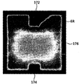
- FIGS. 15A to 15D are images taken while applying an electric current of 350 mA to the light emitting diodes according to Experiment Examples 8 to 11, respectively.
- the light emitting diode showed high light intensity (or power) and also had a relatively low driving voltage when the bonding pad 172 was disposed adjacent to one side 150s-1 of the upper surface of the semiconductor structure 150, and the current distribution pad 174 was disposed opposite to the bonding pad 172, that is, disposed adjacent to another side 150s-2 of the upper surface of the semiconductor structure 150 and had the same shape as the bonding pad 172 (Experiment Example 3), as shown in FIG. 1.
- the light emitting diode showed high light intensity (or power) and also had a relatively low driving voltage when the bonding pad 172 was disposed adjacent to one side 150s-1 of the upper surface of the semiconductor structure 150, and the current distribution pad 174 was disposed opposite to the bonding pad 172, that is, disposed adjacent to another side 150s-2 of the upper surface of the semiconductor structure 150 and had a long overlapping length with the side 150s-2 (Experiment Example 8).
- the light emitting diode showed a relatively high driving voltage when the bonding pad 172 was disposed adjacent to one corner 150c-1 of the upper surface of the semiconductor structure 150 as shown in FIG. 4 or 5 (Experiment Examples 9 and 10).
- the light emitting diode showed a relatively low light intensity (or power) when one extension 176b of the extensions 176 lay across the central region of the upper surface of the semiconductor structure 150 as shown in FIG. 14 (Experiment Example 11).
- Experiment Example 3 the light emitting diode having the configuration as shown in FIG. 1 had an excellent current spreading effect, for example, showing a higher ratio of a region emitting light more strongly than those of the other experiment examples (i.e., a red region, ER in FIG. 11C).
- Experiment Example 8 the light emitting diode having the configuration as shown in FIG. 3 had an excellent current spreading effect, for example, showing a relatively high ratio of a region emitting light more strongly than those of the other experiment examples (i.e., a red region, ER in FIG. 15A).
- the light emitting diode showed good device performance when the bonding pad 172 was disposed adjacent to one side 150s-1 of the upper surface of the semiconductor structure 150, and the current distribution pad 174 was disposed opposite to the bonding pad 172, that is, disposed adjacent to another side 150s-2 of the upper surface of the semiconductor structure 150 and also had the same shape as the bonding pad 172 as shown in FIG.
- FIG. 16 is a schematic plane view showing the light emitting diode according to Experiment Example 13.
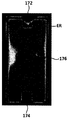
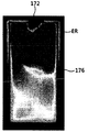
- FIGS. 17A and 17D are images taken while applying an electric current of 1,000 mA to the light emitting diodes according to Experiment Examples 12 to 13, respectively.
- the pad pattern 170 included the current distribution pad 174 facing the bonding pad 172 (Experiment Example 12) as shown in FIG. 6, the light emitting diode had an excellent current spreading effect, for example, showing a lower ratio of a region strongly emitting light(i.e., a red region, ER), compared with when the pad pattern 170 did not include a current distribution pad (Experiment Example 13) as shown in FIG. 16
- FIGS. 18A and 18B are images taken while applying an electric current to the light emitting diode (Experiment Example 14) as shown in FIG. 7 and the light emitting diode (Experiment Example 15) in which a current distribution pad was removed from the light emitting diode as shown in FIG. 7.
Landscapes
- Led Devices (AREA)
Abstract
A light emitting diode is provided. The light emitting diode includes a substrate. A semiconductor structure layer including an active layer is positioned on the substrate. A pad pattern is disposed on an upper surface of the semiconductor structure layer. The pad pattern includes a bonding pad disposed adjacent to a first edge of the upper surface of the semiconductor structure layer, a current distribution pad disposed adjacent to a second edge disposed opposite to the first edge, and extensions configured to electrically connect the bonding pad and the current distribution pad.
Description
Example embodiments of the present invention relate in general to a semiconductor device, and, more specifically, to a light emitting diode.
A light emitting diode (LED) is basically a PN junction diode formed by combining a P-type semiconductor and an N-type semiconductor.
In the LED, when a P-type semiconductor and an N-type semiconductor are combined and a voltage is applied to the P-type and N-type semiconductors, an electric current is allowed to flow through the P-type and N-type semiconductors. In this case, holes of the P-type semiconductor move toward the N-type semiconductor, whereas electrons of the N-type semiconductor move toward the P-type semiconductor, which causes the electrons and holes to move to the PN junction.
The electrons transferred to the PN junction are bound to the holes while falling from a conduction band to a valence band. In this case, the PN junction emits energy corresponding to a difference in height, that is, energy between the conduction band and the valence band. In the process, the energy is emitted in the form of light.
Such an LED is a semiconductor device that emits light and shows characteristics such as environmental friendliness, low voltage, long lifespan and inexpensiveness. In the prior art, the LED was widely applied to a display lamp or display of simple information such as numbers. With the development of industrial technology, particularly, information display technology and semiconductor technology, however, the LED has been used in a variety of fields such display devices, automobile head lamps, projectors, etc.
LEDs may include horizontal LEDs and vertical LEDs. In general, vertical LEDs have excellent current distribution performance compared with horizontal LEDs. That is, horizontal LEDs are formed on a growth substrate for growing an epitaxial layer, and vertical LEDs are positioned on a metal substrate. Therefore, vertical LEDs have an advantage of showing excellent thermal emission performance since they are formed using a metal substrate having high thermal conductivity.
However, vertical LEDs show poor luminous efficiency and short device lifespan because an electric current focuses on a pad region.
Accordingly, example embodiments of the present invention are provided to substantially obviate one or more problems due to limitations and disadvantages of the related art.
Example embodiments of the present invention provide a light emitting diode in which an electric current is uniformly distributed throughout a light emitting region.
Example embodiments of the present invention also provide a light emitting diode having improved lifespan due to uniform current distribution.
In some example embodiments, a light emitting diode is provided. The light emitting diode includes a substrate. A semiconductor structure layer including an active layer is disposed on the substrate. A pad pattern is disposed on an upper surface of the semiconductor structure layer. The pad pattern includes a bonding pad disposed adjacent to a first edge of the upper surface of the semiconductor structure layer, a current distribution pad disposed adjacent to a second edge disposed opposite to the first edge, and extensions configured to electrically connect the bonding pad and the current distribution pad.
A distance between the bonding pad and the first edge may be the same as a distance between the current distribution pad and the second edge. The distance between the bonding pad and the first edge may be in a range of 0.5 to 5% of widths of the light emitting diodes in the same direction. The distance between the bonding pad and the first edge may be in a range of 5 to 40 ㎛. The distance between the current distribution pad and the second edge may be in a range of 0.5 to 5% of the widths of the light emitting diodes in the same direction. The distance between the current distribution pad and the second edge may be in a range of 5 to 40 ㎛.
The first and second edges may be first and second sides of the upper surface of the semiconductor structure layer, respectively. In this case, the bonding pad and the current distribution pad may be disposed at symmetrical positions and formed in the same shape. On the other hand, an overlapping region of the current distribution pad and the second edge may have a higher length than an overlapping region of the bonding pad and the first edge. In addition, the current distribution pad may partially overlap third and fourth edges disposed at both sides of the second edge.
The bonding pad may have the same area as the current distribution pad.
The first and second edges may be first and second corners of the upper surface of semiconductor structure layer, respectively. In this case, the bonding pad and the current distribution pad may be disposed at symmetrical positions and formed in the same shape. On the other hand, the current distribution pad may be a first current distribution pad, and a second current distribution pad may be disposed on at least one of third and fourth corners of the upper surface of the semiconductor structure layer.
The extensions may be disposed adjacent to edges of the upper surface of the semiconductor structure layer. Distance between the extensions and the edges may be in a range of 5 to 40 ㎛. The distance between the extensions and the edges may be in a range of 0.5 to 5% of widths of the light emitting diodes in the same direction. The extensions may not lie across a central region of the semiconductor structure layer.
The bonding pad may not protrude outward relative to the extension adjacent to the bonding pad. A distance between the bonding pad and the first edge may be the same as a distance between the extension and the first edge.
The current distribution pad may not protrude outward relative to the extension adjacent to the current distribution pad. A current distribution pad current distribution pad and the second edge may be the same as a distance between the extension and the second edge.
In other example embodiment, another example of a light emitting diode is provided. The light emitting diode includes a substrate. A semiconductor structure layer including an active layer is disposed on the substrate. A pad pattern is disposed on an upper surface of the semiconductor structure layer. The pad pattern includes a bonding pad disposed adjacent to a first edge of the upper surface of the semiconductor structure layer, a current distribution pad disposed spaced apart from the bonding pad, and extensions configured to electrically connect the bonding pad and the current distribution pad. In this case, the bonding pad does not protrude in a direction of the edges relative to the extension adjacent to the bonding pad.
The distance between the bonding pad and the first edge may be in a range of 0.5 to 5% of widths of the light emitting diodes in the same direction. The distance between the bonding pad and the first edge may be the same as the distance between the extension and the first edge.
The current distribution pad may be disposed adjacent to the other edges other than the first edge of the upper surface of the semiconductor structure layer. A distance between the current distribution pad and an edge adjacent to the current distribution pad may be in a range of 0.5 to 5% of the widths of the light emitting diodes in the same direction. The extensions may be disposed adjacent to the edges of the upper surface of the semiconductor structure layer. Distances between the extensions and the edges may be in a range of 0.5 to 5% of the widths of the light emitting diodes in the same direction. In addition, the extensions may not lie across a central region of the semiconductor structure layer. Meanwhile, the current distribution pad may not protrude outward relative to the extension adjacent to the current distribution pad.
According to example embodiments of the present invention, a light emitting diode having improved current spreading performance can be obtained by respectively disposing a bonding pad and a current distribution pad adjacent to facing edges of an upper surface of the semiconductor structure layer. Also, a light emitting diode having improved current spreading performance can be obtained by disposing the bonding pad adjacent to one of the edges of the upper surface of the semiconductor structure layer and arranging the bonding pad so that the bonding pad cannot protrude toward the edge relative to the extension adjacent to the bonding pad.
The technical effects of the present invention are not limited to those described above, and other technical effects can be clearly understood by those skilled in the art.
Example embodiments of the present invention will become more apparent by describing in detail example embodiments of the present invention with reference to the accompanying drawings, in which:
FIG. 1 is a plane view showing a light emitting diode according to one example embodiment of the present invention.
FIG. 2 is a cross-sectional view taken along line I-I' shown in FIG. 1.
FIG. 3 is a plane view showing a light emitting diode according to another example embodiment of the present invention.
FIG. 4 is a plane view showing a light emitting diode according to still another example embodiment of the present invention.
FIG. 5 is a plane view showing a light emitting diode according to still another example embodiment of the present invention.
FIG. 6 is a plane view showing a light emitting diode according to still another example embodiment of the present invention.
FIG. 7 is a plane view showing a light emitting diode according to still another example embodiment of the present invention.
FIG. 8 is a cross-sectional view taken along line A-A' shown in FIG. 7.
FIG. 9 is a plane view showing a light emitting diode according to still another example embodiment of the present invention.
FIG. 10 is a plane view showing a light emitting diode according to yet another example embodiment of the present invention.
FIGS. 11A to 11D are images taken while allowing an electric current of 350 mA to flow through light emitting diodes according to Experiment Examples 1 to 4, respectively.
FIGS. 12A to 12C are plane views showing light emitting diodes according to Experiment Examples 5 to 7, respectively.
FIGS. 13A to 13C are images taken while allowing an electric current of 350 mA to flow through the light emitting diodes according to Experiment Examples 5 to 7, respectively.
FIG. 14 is a schematic plane view showing a light emitting diode according to Experiment Example 15.
FIGS. 15A to 15D are images taken while allowing an electric current of 350 mA to flow through light emitting diodes according to Experiment Examples 8 to 11, respectively.
FIG. 16 is a schematic plane view showing a light emitting diode according to Experiment Example 12.
FIGS. 17A to 17D are images taken while allowing an electric current of 1,000 mA to flow through light emitting diodes according to Experiment Examples 12 and 13, respectively.
FIGS. 18A and 18B are images taken while allowing an electric current to flow through light emitting diodes according to Experiment Examples 14 and 15, respectively.
Example embodiments of the present invention are disclosed herein. However, specific structural and functional details disclosed herein are merely representative for purposes of describing example embodiments of the present invention, however, example embodiments of the present invention may be embodied in many alternate forms and should not be construed as limited to example embodiments of the present invention set forth herein.
Accordingly, while the invention is susceptible to various modifications and alternative forms, specific example embodiments thereof are shown by way of example in the drawings and will herein be described in detail. It should be understood, however, that there is no intent to limit the invention to the particular forms disclosed, but on the contrary, the invention is to cover all modifications, equivalents, and alternatives falling within the spirit and scope of the invention. Like numbers refer to like elements throughout the description of the figures.
It will be understood that, although the terms first, second, etc. may be used herein to describe various elements, these elements should not be limited by these terms. These terms are only used to distinguish one element from another. For example, a first element could be termed a second element, and, similarly, a second element could be termed a first element, without departing from the scope of the present invention. As used herein, the term "and/or" includes any and all combinations of one or more of the associated listed items.
It will be understood that when an element is referred to as being "connected" or "coupled" to another element, it can be directly connected or coupled to the other element or intervening elements may be present. In contrast, when an element is referred to as being "directly connected" or "directly coupled" to another element, there are no intervening elements present. Other words used to describe the relationship between elements should be interpreted in a like fashion (i.e., "between" versus "directly between," "adjacent" versus "directly adjacent," etc.).
The terminology used herein is for the purpose of describing particular example embodiments only and is not intended to be limiting of the invention. As used herein, the singular forms "a," "an" and "the" are intended to include the plural forms as well, unless the context clearly indicates otherwise. It will be further understood that the terms "comprises," "comprising," "includes" and/or "including," when used herein, specify the presence of stated features, integers, steps, operations, elements, and/or components, but do not preclude the presence or addition of one or more other features, integers, steps, operations, elements, components, and/or groups thereof.
Unless otherwise defined, all terms (including technical and scientific terms) used herein have the same meaning as commonly understood by one of ordinary skill in the art to which this invention belongs. It will be further understood that terms, such as those defined in commonly used dictionaries, should be interpreted as having a meaning that is consistent with their meaning in the context of the relevant art and will not be interpreted in an idealized or overly formal sense unless expressly so defined herein.
FIG. 1 is a plane view showing a light emitting diode according to one example embodiment of the present invention, and FIG. 2 is a cross-sectional view taken along line I-I' shown in FIG. 1.
Referring to FIGS. 1 and 2, the light emitting diode 100 includes a semiconductor structure layer 150 disposed on a supporting substrate 110. A bonding metal layer 120 may be disposed between the supporting substrate 110 and the semiconductor structure layer 150. Also, a current spreading inducing layer 130 including a current interrupting pattern 133 and a current transfer pattern 135 may be disposed between the bonding metal layer 120 and the semiconductor structure layer 150. A pad pattern 170 including a bonding pad 172, a current distribution pad 174 and extensions 176 configured to electrically connect the bonding pad 172 and the current distribution pad 174 may be disposed on an upper surface of the semiconductor structure layer 150.
The semiconductor structure layer 150 may include the first-type semiconductor layer 152, a second-type semiconductor layer 156 and an active layer 154 positioned between the first and second-type semiconductor layers 152 and 156. The first-type semiconductor layer 152 is a nitride-based semiconductor layer that may be doped with an n-type dopant. By way of example, the first-type semiconductor layer 152 may be a layer in which an InxAlyGa1-x-yN (0≤x≤1, 0≤y≤1, and x+y≤1) layer is doped with Si as the n-type dopant. More particularly, the first-type semiconductor layer 152 may be a GaN layer doped with Si. On the other hand, the first-type semiconductor layer 152 may be provided with a plurality of InxAlyGa1-x-yN (0≤x≤1, 0≤y≤1, and x+y≤1) layers having different compositions.
The active layer 154 may be an InxAlyGa1-x-yN (0≤x≤1, 0≤y≤1, and 0≤x+y≤1) layer, and have a single quantum well (SQW) structure or multiple quantum well (MQW) structure. By way of example, the active layer 154 may have an SQW structure of an InGaN layer or an AlGaN layer, or a multi-layered structure, that is, an MQW structure, of InGaN/GaN, AlGaN/(In)GaN or InAlGaN/(In)GaN.
Also, the second-type semiconductor layer 156 may be a nitride-based semiconductor layer, and may be a layer doped with a p-type dopant. By way of example, the second-type semiconductor layer 156 may be a layer in which an InxAlyGa1-x-yN (0≤x≤1, 0≤y≤1, and 0≤x+y≤1) layer is doped with Mg or Zn as the p-type dopant. More particularly, the second-type semiconductor layer 156 may be a GaN layer doped with Mg. On the other hand, the second-type semiconductor layer 156 may be provided with a plurality of InxAlyGa1-x-yN (0≤x≤1, 0≤y≤1, and 0≤x+y≤1) layers having different compositions.
The supporting substrate 110 may be a semiconductor substrate formed of Si, GaAs, GaP, or InP, or a metal substrate formed of Cu or W. The supporting substrate 110 may function to support the semiconductor structure layer 150, and optionally function as an electrode.
The bonding metal layer 120 is a layer that functions to couple the semiconductor structure layer 150 to the supporting substrate 110, and may be a thermo-compressive bonding layer or a eutectic bonding layer. The thermo-compressive bonding layer may be an Au layer/Au layer, and the eutectic bonding layer may be an Au:Sn layer or a Pd:In layer.
As described above, the current spreading inducing layer 130 may include the current interrupting pattern 133 and the current transfer pattern 135. By way of example, these two patterns may be formed adjacent to each other. The current interrupting pattern 133 is a region that functions to prevent an electric current 180 from flowing in a vertical direction of the bonding pad 172, and may be an insulation pattern. By way of example, the current interrupting pattern 133 may be formed of silicon oxide or silicon nitride. The current interrupting pattern 133 may be formed below the bonding pad 172, and also formed below the current distribution pad 174. Further, the current interrupting pattern 133 may be formed below the extensions 176.
Meanwhile, the current transfer pattern 135 is a region that functions to reflect light generated from the active layer 154 while coming in ohmic contact with the semiconductor structure layer 150, particularly, the second-type semiconductor layer 156, and may be a metal pattern. The current transfer pattern 135 may be a single metal film or a multiple metal film formed of a material selected from the group consisting of nickel (Ni), platinum (Pt), palladium (Pd), rhodium (Rh), tungsten (W), titanium (Ti), silver (Ag) and gold (Au).
The bonding pad 172 provided in the pad pattern 170 is disposed adjacent to a first edge of the upper surface of the semiconductor structure layer 150. The current distribution pad 174 is disposed apart from the bonding pad 172, and may be disposed in single or plural number. The bonding pad 172 is a pad to which an electrical interconnection configured to apply an electric source, such as a conductive wire, is connected during packaging of the light emitting diode 100. On the other hand, the current distribution pad 174 is a pad to which no electrical interconnection is connected, and functions to distribute an electric current.
Also, the first edge may refer to one of sides 150s-1, 150s-2, 150s-3 and 150s-4 of the upper surface of the semiconductor structure layer 150, or one of corners 150c-1, 150c-2, 150c-3 and 150c-4 of the upper surface of the semiconductor structure layer 150. As described in this example embodiment, the bonding pad 172 may be disposed adjacent to the first side 150s-1 of the upper surface of the semiconductor structure layer 150. More particularly, the bonding pad 172 may be disposed adjacent to a central region of the first side 150s-1. Meanwhile, the current distribution pad 174 may be disposed adjacent to a second edge positioned opposite to the first edge, particularly, the second side 150s-2 positioned opposite to the first side 150s-1.
A distance D1 between the bonding pad 172 and the first edge 150s-1 of the upper surface of the semiconductor structure layer 150 may be in a range of 5 to 40 ㎛, and may be in a range of 0.5 to 5% of widths 100b of the light emitting diodes 100 in the same direction. Likewise, a distance D2 between the current distribution pad 174 and the second edge 150s-2 of the upper surface of the semiconductor structure layer 150 may be in a range of 5 to 40 ㎛, and may be in a range of 0.5 to 5% of the widths 100b of the light emitting diodes 100 in the same direction.
The bonding pad 172 and the current distribution pad 174 may have substantially the same area, and may be formed in the same shape. Also, the bonding pad 172 and the current distribution pad 174 may be disposed at symmetrical positions.
Widths 176w of the extensions 176 may be 3 to 10% smaller than a width 172w of the bonding pad 172 and a width 174w of the current distribution pad 174. Also, the extensions 176 may be disposed adjacent to the edges of the upper surface of the semiconductor structure layer 150. That is, the extensions 176 may be disposed along the edges of the upper surface of the semiconductor structure layer 150. More particularly, distances De1, De2, De3, De4, De5, De6, De7 and De8 between the extensions 176 and the edges 150s-1, 150s-3, 150s-2, 150s-4, 150c-1, 150c-3, 150c-2 and 150c-4 of the upper surface of the semiconductor structure layer 150 may be in a range of 5 to 40 ㎛. In this case, these distances may be in a range of 0.5 to 5% of widths 100a, 100b, 100c and 100d of the light emitting diodes 100 in the same direction.
Meanwhile, the bonding pad 172 may not protrude to an outside direction relative to the extension 176 connected to the bonding pad 172. That is, the distance D1 between the bonding pad 172 and the first edge 150s-1 of the upper surface of the semiconductor structure layer 150 may be substantially the same as a distance De1 between the extension 176 and the first edge 150s-1 of the supper surface of the semiconductor structure layer 150. Also, the current distribution pad 174 may not protrude to an outside direction relative to the extension 176 connected to the current distribution pad 174. That is, the distance D2 between the current distribution pad 174 and the second edge 150s-2 of the upper surface of the semiconductor structure layer 150 may be substantially the same as a distance De3 between the extension 176 and the first edge 150s-2 of the upper surface of the semiconductor structure layer 150.
The pad pattern 170 may not include extensions other than the extension 176, for example, extensions that do not lie across the central region of the upper surface of the semiconductor structure layer 150. That is, all the extensions provided in the pad pattern 170 may be disposed adjacent to the edges of the upper surface of the semiconductor structure layer 150, or disposed along the edges of the upper surface of the semiconductor structure layer 150, as described above.
The semiconductor structure layer 150 is formed by sequentially stacking the first-type semiconductor layer 152, the active layer 154 and the second-type semiconductor layer 156 on a growth substrate (not shown). Thereafter, the current spreading inducing layer 130 and the bonding metal layer 120 are formed on the second-type semiconductor layer 156, and the supporting substrate 110 is then attached to the bonding metal layer 120. Then, the light emitting diode 100 may be manufactured by removing the growth substrate using a lift-off method such as a laser lift-off (LLO) method or a chemical lift-off (CLO) method, followed by forming the pad pattern 170 on the first-type semiconductor layer 152 that is exposed by removal of the growth substrate. The pad pattern 170 may be an Al layer, a Pt layer, a Ni layer, an Au layer, or a composite layer thereof.
FIG. 3 is a plane view showing a light emitting diode according to another example embodiment of the present invention. The light emitting diode according to this example embodiment has a configuration similar to the light emitting diode described with reference to FIGS. 1 and 2, except for the configurations to be described below.
Referring to FIG. 3, a pad pattern 170 includes a bonding pad 172 disposed adjacent to a first edge of an upper surface of a semiconductor structure layer 150, and at least one current distribution pad 174 spaced apart from the bonding pad 172. The pad pattern 170 may further include extensions 176 configured to electrically connect the bonding pad 172 and the current distribution pad 174.
Also, the first edge may be a first side 150s-1 of the upper surface of the semiconductor structure layer 150. That is, the bonding pad 172 may be disposed adjacent to the first side 150s-1 of the upper surface of the semiconductor structure layer 150. More particularly, the bonding pad 172 may be disposed adjacent to a central region of the first side 150s-1.
Meanwhile, the current distribution pad 174 may be disposed adjacent to a second edge positioned opposite to the first edge, particularly, a second side 150s-2. Unlike the example embodiment described with reference to FIG. 1, however, the current distribution pad 174 may be configured so that an overlapping region of the current distribution pad 174 and the second edge, particularly, the second side 150s-2, can have a higher length than an overlapping region of the bonding pad 172 and the first edge, particularly, the first side 150s-1. In addition, the current distribution pad 174 may extend to partially overlap third and fourth edges disposed at both sides of the second edge, particularly, third and fourth sides 150s-3 and 150s-4. In this case, widths 174w1 and 174w2 of the current distribution pad 174 may be higher than a width 176w of the extension 176. Meanwhile, the current distribution pad 174 may have substantially the same area as the bonding pad 172.
FIG. 4 is a plane view showing a light emitting diode according to still another example embodiment of the present invention. The light emitting diode according to this example embodiment has a configuration similar to the light emitting diode described with reference to FIGS. 1 and 2, except for the configurations to be described below.
Referring to FIG. 4, a pad pattern 170 includes a bonding pad 172 disposed adjacent to a first edge of an upper surface of a semiconductor structure layer 150, and at least one current distribution pad 174 spaced apart from the bonding pad 172. The pad pattern 170 may further include extensions 176 configured to electrically connect the bonding pad 172 and the current distribution pad 174.
The first edge may be a first corner 150c-1 of the upper surface of the semiconductor structure layer 150. That is, the bonding pad 172 may be disposed adjacent to a first corner 150c-1 of the upper surface of the semiconductor structure layer 150. Meanwhile, the current distribution pad 174 may be disposed adjacent to a second edge positioned opposite to the first edge, particularly, a second corner 150s-2.
Also, the bonding pad 172 and the current distribution pad 174 may have substantially the same area, and may be formed in the same shape. Also, the bonding pad 172 and the current distribution pad 174 may disposed at symmetrical positions.
FIG. 5 is a plane view showing a light emitting diode according to still another example embodiment of the present invention. The light emitting diode according to this example embodiment has a configuration similar to the light emitting diode described with reference to FIGS. 1 and 2, except for the configurations to be described below.
Referring to FIG. 5, a pad pattern 170 includes a bonding pad 172 disposed adjacent to a first edge of an upper surface of a semiconductor structure layer 150, and at least one current distribution pad 174 spaced apart from the bonding pad 172. The pad pattern 170 may further include extensions 176 configured to electrically connect the bonding pad 172 and the current distribution pad 174.
The first edge may be a first corner 150c-1 of the upper surface of the semiconductor structure layer 150. That is, the bonding pad 172 may be disposed adjacent to the first corner 150c-1 of the upper surface of the semiconductor structure layer 150.
Meanwhile, the current distribution pad 174 may include a first current distribution pad 174a disposed adjacent to a second edge positioned opposite to the first edge, particularly, a second corner 150s-2, and second and third current distribution pads 174b and 174c disposed respectively at the other corners 150c-3 and 150c-4 of the upper surface of the semiconductor structure layer 150.
Also, the bonding pad 172 and the first and third current distribution pads 174a, 174b and 174c may be formed in the same shape, and the bonding pad 172 may have substantially the same area as the sum of areas of the first and third current distribution pads 174a, 174b and 174c.
FIG. 6 is a plane view showing a light emitting diode according to still another example embodiment of the present invention. The light emitting diode according to this example embodiment has a configuration similar to the light emitting diode described with reference to FIGS. 1 and 2, except for the configurations to be described below.
As shown in FIG. 1, a ratio of the width 100a of the light emitting diode in the first direction and the width 100b of the light emitting diode in the second direction is close to 1:1, whereas, the light emitting diode as shown in FIG. 6 may be formed to have a higher width 100b in the second direction than a width 100a in the first direction. By way of example, referring to FIG. 6, a ratio of the width 100a in the first direction and the width 100b in the second direction may be in a range of approximately 1:1.5 to 1:2.
FIG. 7 is a plane view showing a light emitting diode according to still another example embodiment of the present invention. FIG. 8 is a cross-sectional view taken along line A-A' as shown in FIG. 7.
Referring to FIGS. 7 and 8, a light emitting diode 100 according to this example embodiment may include a supporting substrate 110, a bonding metal layer 120, a current spreading inducing layer 130, a semiconductor structure layer 150, a passivation layer 160 and a pad pattern 170. The pad pattern 170 may include a bonding pad 172, a current distribution pad 174, and extensions 176 configured to electrically connect the bonding pad 172 and the current distribution pad 174.
The supporting substrate 110 may be a substrate that functions to support the semiconductor structure layer 150, for example, a conductive substrate. Also, the supporting substrate 110 may function to apply an electric source to the light emitting diode 100, particularly, the semiconductor structure layer 150, that is, may act as an electrode of the light emitting diode 100.
The bonding metal layer 120 is interposed between the supporting substrate 110 and a current spreading inducing layer 130 (or a semiconductor structure layer 150) positioned on the supporting substrate 110, and thus functions to couple the supporting substrate 110 and the current spreading inducing layer 130.
The current spreading inducing layer 130 may include a current interrupting pattern 133 and a current transfer pattern 135. In this case, the current interrupting pattern 133 may include an open region, and may be formed in a shape in which the current transfer pattern 135 is filled in the open region of the current interrupting pattern 133.
The current interrupting pattern 133 functions to prevent an electric current 180 supplied from the bonding pad 172, the current distribution pad 174 and the extension 176 from flowing in a vertical direction of the pad pattern 170, thereby allowing the electric current 180 to uniformly flow in the semiconductor structure layer 150, preferably, throughout the active layer 154. That is, the current interrupting pattern 133 functions to sufficiently distribute the electric current 180 supplied to the semiconductor structure layer 150 in the first-type semiconductor layer 152 of the semiconductor structure layer 150 so as to supply the electric current 180 to the active layer 154 provided below the first-type semiconductor layer 152. Also, the current interrupting pattern 133 may function to give information on an etching end point so as to form the semiconductor structure layer 150 during manufacture of the light emitting diode 100. The current interrupting pattern 133 may be formed of an insulating material, and may be composed of a silicon oxide film or a silicon nitride film.
The current transfer pattern 135 may include a material that comes in ohmic contact with the second-type semiconductor layer 156, and reflect light emitted from the active layer 154. The current transfer pattern 135 may be referred to as an ohmic reflective metal pattern. For example, when the second-type semiconductor layer 156 is a P-type semiconductor, the current transfer pattern 135 may be formed of a material such as nickel (Ni), platinum (Pt), palladium (Pd), rhodium (Rh), tungsten (W), titanium (Ti), silver (Ag) or gold (Au), which may come in ohmic contact with the P-type semiconductor.
Meanwhile, the bonding metal layer 120 may function to maintain the reflectivity of the current transfer pattern 135 by preventing metal elements from being distributed from the supporting substrate 110 to the current transfer pattern 135. Also, a Schottky barrier metal layer (not shown) may be disposed between the bonding metal layer 120 and the current interrupting pattern 133.
The semiconductor structure layer 150 may include a first-type semiconductor layer 152, an active layer 154 and a second-type semiconductor layer 156. Here, the second-type semiconductor layer 156 may be formed on the current spreading inducing layer 130, the active layer 154 may be formed on the second-type semiconductor layer 156, and the first-type semiconductor layer 152 may be formed on the active layer 154. Also, the semiconductor structure layer 150 may further include a superlattice layer (not shown) or an electron blocking layer (not shown). Layers other than the active layer 154 may be omitted in the semiconductor structure layer 150.
The first-type semiconductor layer 152 may be a III-N-based compound semiconductor doped with first-type impurities, for example, N-type impurities, for example, an (Al, Ga, In) N-based Group III nitride semiconductor layer. The first-type semiconductor layer 152 may be a GaN layer doped with N-type impurities, that is, an N-GaN layer. Also, the first-type semiconductor layer 152 may have a single-layered or multi-layered structure. For example, when the first-typesemiconductor layer 152 is formed in a multi-layered structure, the first-type semiconductor layer 152 may have a superlattice structure.
The active layer 154 may be composed of a III-N-based compound semiconductor, for example, an (Al, Ga, In) N semiconductor layer. Here, the active layer 154 may be formed of a single layer or multiple layers, and thus may emit light of predetermined wavelengths. Also, the active layer 154 may have an SQW structure including one well layer (not shown), and may have an MQW structure in which well layers (not shown) and barrier layers (not shown) are alternately stacked with each other. In this case, one or both of the well layer (not shown) or barrier layer (not shown) may be formed with a superlattice structure.
The second-type semiconductor layer 156 may be a III-N-based compound semiconductor doped with second-type impurities, for example, P-type impurities, for example, an (Al, In, Ga) N-based Group III nitride semiconductor. The second-type semiconductor layer 156 may be a GaN layer doped with P-type impurities, that is, a P-GaN layer. Also, the second-type semiconductor layer 156 may be formed with a single-layered or multiple-layered structure. For example, the second-type semiconductor layer 156 may be formed with a superlattice structure.
The superlattice layer (not shown) may be provided between the first type semiconductor layer 152 and the active layer 154, and may have a structure including layers formed by stacking a plurality of III-N-based compound semiconductors, for example, (Al, Ga, In) N semiconductor layers, for example, repeatedly stacking InN layers and InGaN layers. In this case, the superlattice layer (not shown) is formed prior to formation of the active layer 154 to prevent dislocations or defects from being transferred to the active layer 154. As a result, the superlattice layer (not shown) may function to reduce formation of the dislocations or defects of the active layer 154 and maintain excellent crystallinity of the active layer 154.
The electron blocking layer (not shown) may be provided between the active layer 154 and the second-type semiconductor layer 156. In this case, an electron blocking layer (not shown) may be provided to enhance recombination efficiency of electrons and holes and formed of a material having a relatively wide band gap. The electron blocking layer (not shown) may be formed from an (Al, In, Ga) N-based Group III nitride semiconductor, and made of a P-AlGaN layer doped with Mg.
The passivation layer 160 may be formed on one surface of the supporting substrate 110 including the semiconductor structure layer 150. In this case, the passivation layer 160 may function to protect the semiconductor structure layer 150 by covering lateral surfaces as well as one surface of the semiconductor structure layer 150 to prevent the semiconductor structure layer 150 from being exposed to the outside. The passivation layer 160 may be made of an insulation film such as a silicon oxide film or a silicon nitride film. Meanwhile, the passivation layer 160 may include an opening 162 configured to expose a certain region of the first conductive semiconductor layer 152.
The pad pattern 170 may be formed on the passivation layer 160. In this case, FIG. 8 shows that the pad pattern 170 is formed on the passivation layer 160. However, the pad pattern 170 may be provided between the semiconductor structure layer 150 and the passivation layer 160, that is, may be provided so that the passivation layer 160 can cover the pad pattern 170. In this case, the passivation layer 160 may have an opening configured to open the bonding pad 172 of the pad pattern 170.
The bonding pad 172 of the pad pattern 170 may be formed on a certain region of the passivation layer 160, preferably one edge of a surface of the semiconductor structure layer 150. The bonding pad 172 may be connected with an external device or an external electric source through a wire (not shown). That is, the light emitting diode 100, particularly, the semiconductor structure layer 150, according to one example embodiment of the present invention is connected to an external electric source through the bonding pad 172. The current interrupting pattern 133 may be positioned just under the bonding pad 172.
In this case, the bonding pad 172 may have a smaller size than the current interrupting pattern 133. That is, the bonding pad 172 may be provided so that a width of the bonding pad 172 can be smaller than that of the current interrupting pattern 133.
The current distribution pad 174 of the pad pattern 170 is formed in plural number on a certain region of the passivation layer 160. In this case, the current distribution pad 174 may be provided to be spaced apart from the bonding pad 172. The current distribution pad 174 may be formed on one edge of the surface of the semiconductor structure layer 150 other than the one edge of the surface of the semiconductor structure layer 150 on which the bonding pad 172 is positioned. That is, when the bonding pad 172 is positioned on one edge of the surface of the semiconductor structure layer 150 as shown in FIG. 7, the current distribution pad 174 may be formed on the other edge of the surface of the semiconductor structure layer 150 that is positioned opposite the one edge on which the bonding pad 172 is positioned.
Like the bonding pad 172, the current interrupting pattern 133 may be positioned just under the current distribution pad 174. Therefore, the current interrupting pattern 133 may be provided so that an electric current injected from the current distribution pad 174 to the semiconductor structure layer 150 cannot focus in a vertical direction of the current distribution pad 174 but can be spread within the semiconductor structure layer 150. The current distribution pad 174 may have a size identical to or smaller than that of the bonding pad 172. The current distribution pad 174 is formed to a wider width than the extension 176.
The extensions 176 of the pad pattern 170 may be formed on the semiconductor structure layer 150. The extensions 176 may be connected to the bonding pad 172, and may be provided to be uniformly distributed on the semiconductor structure layer 150. That is, the extensions 176 may be arranged along the edges on the surface of the semiconductor structure layer 150 surface, and arranged across the central region.
The extensions 176 are connected to the bonding pad 172 to uniformly distribute an electric source supplied from the outside in the semiconductor structure layer 150, and thus function to inject the electric source into the semiconductor structure layer 150. The extensions 176 function to electrically connect the bonding pad 172 and the current distribution pad 174. Like the bonding pad 172, the extensions 176 may be provided in a shape in which the current interrupting pattern 130 is positioned just under the extensions 17.
In summary, the light emitting diode 100 according to this example embodiment includes a pad pattern 170, which includes the bonding pad 172, the current distribution pad 174 and the extensions 176, all of which are formed on the semiconductor structure layer 150. When the current interrupting pattern 133 is disposed under at least the bonding pad 172 and the current distribution pad 174 of the pad pattern 170, an electric current flowing through the semiconductor structure layer 150 is allowed to uniformly flow by interaction between the bonding pad 172 and current distribution pad 174 and the current interrupting pattern 133, thereby uniformly emitting light all over the semiconductor structure layer 150.
FIG. 9 is a plane view showing a light emitting diode according to still another example embodiment of the present invention.
Referring to FIG. 9, the light emitting diode 100 according to this example embodiment is different from the light emitting diode 100 described with reference to FIGS. 7 and 8 in that the current distribution pad 174 may be provided on edges other than the one edge of the surface of the semiconductor structure layer 150. That is, the current distribution pad 174 may be disposed on another edge on which the bonding pad 172 is provided among the edges of the semiconductor structure layer 150.
FIG. 10 is a plane view showing a light emitting diode according to yet another example embodiment of the present invention.
Referring to FIG. 10, the light emitting diode 100 according to this example embodiment is different from the light emitting diode 100 described with reference to FIGS. 7 and 8 in that the current distribution pad 174 may be provided on a central region of the surface of the semiconductor structure layer 150. That is, the light emitting diode 100 according to this example embodiment may have a structure in which the current distribution pad 174 is disposed on a certain region on the surface of the semiconductor structure layer 150 other than the edges of the semiconductor structure layer 150.
Hereinafter, experiment examples of the present invention will be described in detail for better understanding of the invention. However, it should be understood that the following examples are only illustrative for better understanding of the invention, and are not intended to limit the scope of the present invention.
Comparison of device performances according to change in area of current distribution pad
In the light emitting diode as shown in FIG. 1, the area of the current distribution pad 174 was set to amount to 60% (Experiment Example 1), 80% (Experiment Example 2), 100% (Experiment Example 3), and 150% (Experiment Example 4) of the bonding pad 172, and the driving voltage and power were measured. The results are listed in the following Table 1. Also, FIGS. 11A to 11D are images taken while applying an electric current of 350 mA to the light emitting diodes according to Experiment Examples 1 to 4, respectively.
Table 1
| (Area of current distribution pad/area of bonding pad) | light intensity [mW] | Driving voltage (Vf)[V] | |
| Experiment Example 1 | 60% | 445.4 | 3.81 |
| Experiment Example 2 | 80% | 444.9 | 3.80 |
| Experiment Example 3 | 100% | 446.0 | 3.79 |
| Experiment Example 4 | 150% | 443.7 | 3.78 |
As listed in Table 1, it was confirmed that, when the area of the current distribution pad was identical to that of the bonding pad (Experiment Example 3), the light emitting diode showed the most excellent light intensity (or power) and also had a relatively low driving voltage. However, when the area of the current distribution pad was smaller than that of the bonding pad (Experiment Examples 1 and 2), the light emitting diode showed a lower light intensity than that of Experiment Example 3 and also had a relatively high driving voltage. Also, when the area of the current distribution pad was higher than that of the bonding pad (Experiment Example 4), the light emitting diode showed a lower light intensity than that of Experiment Example 3.
Referring to FIGS. 11A to 11D, it was revealed that the light emitting diode had an excellent current spreading effect, for example, showing a higher ratio of a region emitting light more strongly than those of the other experiment examples (i.e., a red region, ER), when the area of the current distribution pad was identical to that of the bonding pad (see Experiment Example 3 and FIG. 11C).
From these results, it could be seen that, when the area of the current distribution pad was identical to that of the bonding pad, the light emitting diode showed better device performance, compared with when the area of the current distribution pad was not identical to that of the bonding pad.
Comparison of device performance according to change in position of extensions
In the light emitting diode as shown in FIG. 1, the distance D1 between the bonding pad 172 and the edge of the upper surface of the semiconductor structure layer 150 and the distance D2 between the current distribution pad 174 and the edge of the upper surface of the semiconductor structure layer 150 were set to a fixed value of 24 ㎛, and the distances (De1, De2, De3, and De4) between the extensions and the edges of the upper surface of the semiconductor structure layer 150 were set respectively to 24 ㎛ (Experiment Example 3), 39 ㎛ (Experiment Example 5), 54 ㎛ (Experiment Example 6), and 69 ㎛ (Experiment Example 7). Then, the driving voltage and power were measured. The results are listed in the following Table 2. Also, FIGS. 12A to 12C are plane views showing the light emitting diodes according to Experiment Examples 5 to 7, respectively, and FIGS. 13A to 13C are images taken while applying an electric current of 350 mA to the light emitting diodes according to Experiment Examples 5 to 7, respectively. In Experiment Examples 3 and 5 to 7, the area of the current distribution pad was set to the same area as the bonding pad.
Table 2
| Distance between bonding pad (or current distribution pad) and edge of upper surface of semiconductor structure layer | Distance between extensions and edges of upper surface of semiconductor structure layer | Light intensity[mW] | Driving voltage (Vf)[V] | |
| Experiment Example 3 | 24 ㎛ | 24 ㎛ | 446.0 | 3.79 |
| Experiment Example 5 | 39 ㎛ | 425.6 | 3.80 | |
| Experiment Example 6 | 54 ㎛ | 420.1 | 3.79 | |
| Experiment Example 7 | 69 ㎛ | 422.9 | 3.77 |
As listed in Table 2, it was confirmed that, when the bonding pad or the current distribution pad did not protrude from the light emitting diode relative to the extension (Experiment Example 3), the light emitting diode showed the most excellent light intensity (or power) and also had a relatively low driving voltage. However, when the bonding pad or current distribution pad protruded from the light emitting diode relative to the extension, that is, the extension moved to be disposed to the central direction of the upper surface of the light emitting diode (Experiment Examples 5, 6, and 7), the light emitting diode showed a drastically reduced light intensity, compared with that of Experiment Example 3.
Referring to FIG. 11C (Experiment Example 3), and FIGS. 13A to 13C (Experiment Examples 5, 6 and 7), it was revealed that, when the bonding pad or the current distribution pad protruded outward relative to the extension (FIGS. 13A to 13C), the light emitting diode had a poor current spreading effect, for example, showing a lower ratio of a region strongly emitting light (i.e., a red region, ER), compared with when the bonding pad or the current distribution pad did not protrude outward relative to the extension (FIG. 11C). In this case, it was confirmed that the ratio of the region strongly emitting light (i.e., a red region, ER) reduced as the bonding pad or the current distribution pad increasingly protruded outward relative to the extension.
From these results, it could be seen that the light emitting diode showed good device performance when the bonding pad or the current distribution pad did not protrude from the light emitting diode relative to the extension, that is, the distance between the bonding pad (or a current distribution pad) and the edge of the upper surface of the semiconductor structure layer was identical to the distance between the extension and the edge of the upper surface of the semiconductor structure layer.
Comparison of device performance according to changes in positions and shapes of bonding pad, current distribution pad and extensions
The driving voltages and powers of the light emitting diodes as shown in FIG. 1 (Experiment Example 1), FIGS. 3 to 5 (Experiment Examples 8, 9 and 10), and FIG. 14 (Experiment Example 11) were measured. The results are listed in the following Table 3. FIGS. 15A to 15D are images taken while applying an electric current of 350 mA to the light emitting diodes according to Experiment Examples 8 to 11, respectively.
Table 3
| Bonding pad | Current distribution pad | Extensions | Power[mW] | Driving voltage (Vf)[V] | |
| Experiment Example 3(FIG. 1) | Adjacent to one side of upper surface of semiconductor structure | Adjacent to opposite side of bonding pad and formed in same shape | Formed adjacent to edge of upper surface of semiconductor structure | 446.0 | 3.79 |
| Experiment Example 8(FIG. 3) | Adjacent to opposite side of bonding pad, but having higher overlapping length with sides (having same area as bonding pad) | 447.1 | 3.78 | ||
| Experiment Example 9(FIG. 4) | Adjacent to one corner of upper surface of semiconductor structure | Adjacent to opposite corner of bonding pad and formed in same shape | 447.1 | 3.86 | |
| Experiment Example 10(FIG. 5) | Formed in plural number on opposite corner of bonding pad and other corners (having same area as sum of areas of bonding pads) | 449.5 | 3.86 | ||
| Experiment Example 11(FIG. 14) | Adjacent to one side of upper surface of semiconductor structure | - | Lying across central region of upper surface of semiconductor structure | 444.7 | 3.75 |
As listed in Table 3, it was confirmed that the light emitting diode showed high light intensity (or power) and also had a relatively low driving voltage when the bonding pad 172 was disposed adjacent to one side 150s-1 of the upper surface of the semiconductor structure 150, and the current distribution pad 174 was disposed opposite to the bonding pad 172, that is, disposed adjacent to another side 150s-2 of the upper surface of the semiconductor structure 150 and had the same shape as the bonding pad 172 (Experiment Example 3), as shown in FIG. 1.
As shown in FIG. 3, it was also confirmed that the light emitting diode showed high light intensity (or power) and also had a relatively low driving voltage when the bonding pad 172 was disposed adjacent to one side 150s-1 of the upper surface of the semiconductor structure 150, and the current distribution pad 174 was disposed opposite to the bonding pad 172, that is, disposed adjacent to another side 150s-2 of the upper surface of the semiconductor structure 150 and had a long overlapping length with the side 150s-2 (Experiment Example 8).
Meanwhile, the light emitting diode showed a relatively high driving voltage when the bonding pad 172 was disposed adjacent to one corner 150c-1 of the upper surface of the semiconductor structure 150 as shown in FIG. 4 or 5 (Experiment Examples 9 and 10).
Also, the light emitting diode showed a relatively low light intensity (or power) when one extension 176b of the extensions 176 lay across the central region of the upper surface of the semiconductor structure 150 as shown in FIG. 14 (Experiment Example 11).
Referring to FIG. 11C (Experiment Example 3), and FIGS. 15A to 15D (Experiment Examples 8 to 11), it was revealed that Experiment Example 3 (the light emitting diode having the configuration as shown in FIG. 1) had an excellent current spreading effect, for example, showing a higher ratio of a region emitting light more strongly than those of the other experiment examples (i.e., a red region, ER in FIG. 11C). However, it was also revealed that Experiment Example 8 (the light emitting diode having the configuration as shown in FIG. 3) had an excellent current spreading effect, for example, showing a relatively high ratio of a region emitting light more strongly than those of the other experiment examples (i.e., a red region, ER in FIG. 15A).
From these results, it could be seen that the light emitting diode showed good device performance when the bonding pad 172 was disposed adjacent to one side 150s-1 of the upper surface of the semiconductor structure 150, and the current distribution pad 174 was disposed opposite to the bonding pad 172, that is, disposed adjacent to another side 150s-2 of the upper surface of the semiconductor structure 150 and also had the same shape as the bonding pad 172 as shown in FIG. 1 (Experiment Example 3), or when the bonding pad 172 was disposed adjacent to one side 150s-1 of the upper surface of the semiconductor structure 150, and the current distribution pad 174 was disposed opposite to the bonding pad 172, that is, disposed adjacent to another side 150s-2 of the upper surface of the semiconductor structure 150 and had an longer overlapping length with the side 150s-2 (Experiment Example 8) than the bonding pad 172.
Comparison of device performance according to presence/absence of current distribution pad
The driving voltages and powers of the light emitting diodes as shown in FIG. 6 (Experiment Example 12) and FIG. 16 (Experiment Example 13) were measured. The results are listed in the following Table 4. FIG. 16 is a schematic plane view showing the light emitting diode according to Experiment Example 13. Also, FIGS. 17A and 17D are images taken while applying an electric current of 1,000 mA to the light emitting diodes according to Experiment Examples 12 to 13, respectively.
Table 4
| Bonding pad | Current distribution pad | Power[mW] | Driving voltage (Vf)[V] | |
| Experiment Example 12(FIG. 6) | Adjacent to one side of upper surface of semiconductor structure | Adjacent to opposite side of bonding pad and formed in same shape | 426.61 | 3.57 |
| Experiment Example 13(FIG. 16) | - | 433.60 | 3.67 |
As shown in Table 4, it was revealed that, when the pad pattern 170 included the current distribution pad 174 facing the bonding pad 172 as shown in FIG. 6, the light emitting diode showed a relatively lower driving voltage, compared with when the pad pattern 170 did not include a current distribution pad as shown in FIG. 16.
Referring to FIG. 17A (Experiment Example 12) and FIG. 17B (Experiment Example 13), when the pad pattern 170 included the current distribution pad 174 facing the bonding pad 172 (Experiment Example 12) as shown in FIG. 6, the light emitting diode had an excellent current spreading effect, for example, showing a lower ratio of a region strongly emitting light(i.e., a red region, ER), compared with when the pad pattern 170 did not include a current distribution pad (Experiment Example 13) as shown in FIG. 16
From these results, it could be seen that, when the pad pattern 170 included the current distribution pad 174 facing the bonding pad 172 (Experiment Example 12) as shown in FIG. 6, the light emitting diode showed good device performance, compared with when the pad pattern 170 did not include a current distribution pad (Experiment Example 13) as shown in FIG. 16.
FIGS. 18A and 18B are images taken while applying an electric current to the light emitting diode (Experiment Example 14) as shown in FIG. 7 and the light emitting diode (Experiment Example 15) in which a current distribution pad was removed from the light emitting diode as shown in FIG. 7.
Referring FIG. 18B, it could be seen that, in the case of the light emitting diode (Experiment Example 15) from which the current distribution pad was removed, an electric current focused on a certain region, particularly, a region 190 adjacent to the bonding pad 172 (see FIG. 7) so that the region 190 could emit stronger light than other regions.
Referring FIG. 18A, it could be seen that, in the case of the light emitting diode (Experiment Example 14) including the current distribution pad, light was relatively uniformly emitted from a region in which the current distribution pad 174 was disposed, as well as a region in which the bonding pad 172 was disposed, for example, light was relatively uniformly emitted from an entire region of the pad pattern. That is, it could be seen that the light emitting diode including the current distribution pad showed uniform current distribution over the semiconductor structure layer, that is, the entire light emitting region.
While the example embodiments of the present invention and their advantages have been described in detail, it should be understood that various changes, substitutions and alterations may be made herein without departing from the scope of the invention.
Claims (31)
- A light emitting diode comprising:a substrate;a semiconductor structure layer which is positioned on the substrate and includes an active layer; anda pad pattern including a bonding pad disposed adjacent to a first edge of an upper surface of the semiconductor structure layer, a current distribution pad disposed adjacent to a second edge opposite to the first edge and extensions configured to electrically connect the bonding pad and the current distribution pad.
- The light emitting diode of claim 1, wherein a distance between the bonding pad and the first edge is the same as a distance between the current distribution pad and the second edge.
- The light emitting diode of claim 1 or 2, wherein the distance between the bonding pad and the first edge is in a range of 0.5 to 5% of widths of the light emitting diodes in the same direction.
- The light emitting diode of claim 1 or 2, wherein the distance between the bonding pad and the first edge is in a range of 5 to 40 ㎛.
- The light emitting diode of claim 1, wherein the distance between the current distribution pad and the second edge is in a range of 0.5 to 5% of the widths of the light emitting diodes in the same direction.
- The light emitting diode of claim 1, wherein the distance between the current distribution pad and the second edge is in a range of 5 to 40 ㎛.
- The light emitting diode of claim 1, wherein the first and second edges are first and second sides of the upper surface of the semiconductor structure layer, respectively.
- The light emitting diode of claim 7, wherein the bonding pad and the current distribution pad are disposed at symmetrical positions and formed in the same shape.
- The light emitting diode of claim 7, wherein an overlapping region of the current distribution pad and the second edge has a higher length than an overlapping region of the bonding pad and the first edge.
- The light emitting diode of claim 9, wherein the current distribution pad partially overlaps third and fourth edges disposed at both sides of the second edge.
- The light emitting diode of any one of claims 1 to 9, wherein the bonding pad has the same area as the current distribution pad.
- The light emitting diode of claim 1, wherein the first and second edges are first and second corners of the upper surface of the semiconductor structure layer, respectively.
- The light emitting diode of claim 12, wherein the bonding pad and the current distribution pad are disposed at symmetrical positions and formed in the same shape.
- The light emitting diode of claim 12, wherein the current distribution pad is a first current distribution pad, andwhich further comprises a second current distribution pad disposed on at least one of third and fourth corners of the upper surface of the semiconductor structure layer.
- The light emitting diode of claim 1, wherein the extensions are disposed adjacent to the edges of the upper surface of the semiconductor structure layer.
- The light emitting diode of claim 15, wherein distances between the extensions and the edges are in a range of 5 to 40 ㎛.
- The light emitting diode of claim 15, wherein the distances between the extensions and the edges are in a range of 0.5 to 5% of the widths of the light emitting diodes in the same direction.
- The light emitting diode of claim 15, wherein the extensions do not lie across a central region of the semiconductor structure layer.
- The light emitting diode of claim 1, wherein the bonding pad does not protrude outward relative to the extension adjacent to the bonding pad.
- The light emitting diode of claim 19, wherein a distance between the bonding pad and the first edge is the same as a distance between the extension and the first edge.
- The light emitting diode of claim 1, wherein the current distribution pad does not protrude outward relative to the extension adjacent to the current distribution pad.
- The light emitting diode of claim 21, wherein a distance between the current distribution pad and the second edge is the same as a distance between the extension and the second edge.
- A light emitting diode comprising:a substrate;a semiconductor structure layer which is positioned on the substrate and includes an active layer; anda pad pattern including a bonding pad disposed adjacent to a first edge of an upper surface of the semiconductor structure layer, a current distribution pad disposed apart from the bonding pad and extensions configured to electrically connect the bonding pad and the current distribution pad,wherein the bonding pad does not protrude in a direction of the edges relative to the extension adjacent to the bonding pad.
- The light emitting diode of claim 23, wherein a distance between the bonding pad and the first edge is in a range of 0.5 to 5% of widths of the light emitting diodes in the same direction.
- The light emitting diode of claim 23 or 24, wherein the distance between the bonding pad and the first edge is the same as a distance between the extension and the first edge.
- The light emitting diode of claim 23, wherein the current distribution pad is disposed adjacent to the other edges other than the first edge of the upper surface of the semiconductor structure layer.
- The light emitting diode of claim 26, wherein a distance between the current distribution pad and an edge adjacent to the current distribution pad is in a range of 0.5 to 5% of the widths of the light emitting diodes in the same direction.
- The light emitting diode of claim 26, wherein the extensions are disposed adjacent to the edges of the upper surface of the semiconductor structure layer.
- The light emitting diode of claim 28, wherein distances between the extensions and the edges are in a range of 0.5 to 5% of the widths of the light emitting diodes in the same direction.
- The light emitting diode of claim 28, wherein the extensions do not lie across a central region of the semiconductor structure layer.
- The light emitting diode of claim 26, wherein the current distribution pad does not protrude outward relative to the extension adjacent to the current distribution pad.
Applications Claiming Priority (4)
| Application Number | Priority Date | Filing Date | Title |
|---|---|---|---|
| KR1020110130998A KR20130064407A (en) | 2011-12-08 | 2011-12-08 | Light emitting diode |
| KR10-2011-0130998 | 2011-12-08 | ||
| KR10-2012-0134013 | 2012-11-23 | ||
| KR1020120134013A KR20140066591A (en) | 2012-11-23 | 2012-11-23 | Light emitting device with improved current spreading |
Publications (1)
| Publication Number | Publication Date |
|---|---|
| WO2013085255A1 true WO2013085255A1 (en) | 2013-06-13 |
Family
ID=48574550
Family Applications (1)
| Application Number | Title | Priority Date | Filing Date |
|---|---|---|---|
| PCT/KR2012/010436 Ceased WO2013085255A1 (en) | 2011-12-08 | 2012-12-04 | Light emitting diode with improved current spreading |
Country Status (1)
| Country | Link |
|---|---|
| WO (1) | WO2013085255A1 (en) |
Cited By (1)
| Publication number | Priority date | Publication date | Assignee | Title |
|---|---|---|---|---|
| US20170365743A1 (en) * | 2016-06-16 | 2017-12-21 | Seoul Viosys Co., Ltd. | Vertical light emitting diode having electrode configuration and light emitting diode package having the same |
Citations (5)
| Publication number | Priority date | Publication date | Assignee | Title |
|---|---|---|---|---|
| KR100665120B1 (en) * | 2005-02-28 | 2007-01-09 | 삼성전기주식회사 | Vertical structure nitride semiconductor light emitting device |
| JP2009302201A (en) * | 2008-06-11 | 2009-12-24 | Toyoda Gosei Co Ltd | Group iii nitride semiconductor light emitting element |
| KR101012823B1 (en) * | 2009-02-19 | 2011-02-08 | 주식회사 세미콘라이트 | Nitride-based light emitting device |
| KR101048912B1 (en) * | 2010-12-17 | 2011-07-12 | (주)더리즈 | Light emitting element |
| KR20110101573A (en) * | 2010-03-09 | 2011-09-16 | 엘지디스플레이 주식회사 | Nitride semiconductor light emitting device |
-
2012
- 2012-12-04 WO PCT/KR2012/010436 patent/WO2013085255A1/en not_active Ceased
Patent Citations (5)
| Publication number | Priority date | Publication date | Assignee | Title |
|---|---|---|---|---|
| KR100665120B1 (en) * | 2005-02-28 | 2007-01-09 | 삼성전기주식회사 | Vertical structure nitride semiconductor light emitting device |
| JP2009302201A (en) * | 2008-06-11 | 2009-12-24 | Toyoda Gosei Co Ltd | Group iii nitride semiconductor light emitting element |
| KR101012823B1 (en) * | 2009-02-19 | 2011-02-08 | 주식회사 세미콘라이트 | Nitride-based light emitting device |
| KR20110101573A (en) * | 2010-03-09 | 2011-09-16 | 엘지디스플레이 주식회사 | Nitride semiconductor light emitting device |
| KR101048912B1 (en) * | 2010-12-17 | 2011-07-12 | (주)더리즈 | Light emitting element |
Cited By (6)
| Publication number | Priority date | Publication date | Assignee | Title |
|---|---|---|---|---|
| US20170365743A1 (en) * | 2016-06-16 | 2017-12-21 | Seoul Viosys Co., Ltd. | Vertical light emitting diode having electrode configuration and light emitting diode package having the same |
| KR20170142054A (en) * | 2016-06-16 | 2017-12-27 | 서울바이오시스 주식회사 | Vertical light emitting diode having electrode configuration and light emitting diode package having the same |
| CN107527975A (en) * | 2016-06-16 | 2017-12-29 | 首尔伟傲世有限公司 | Vertical type light emitting diode and light emission diode package member with electrode structure |
| US10283675B2 (en) * | 2016-06-16 | 2019-05-07 | Seoul Viosys Co., Ltd. | Vertical light emitting diode having electrode configuration and light emitting diode package having the same |
| KR102554231B1 (en) * | 2016-06-16 | 2023-07-12 | 서울바이오시스 주식회사 | Vertical light emitting diode having electrode configuration and light emitting diode package having the same |
| DE102017210114B4 (en) | 2016-06-16 | 2026-04-02 | Seoul Viosys Co., Ltd | VERTICAL LIGHT-EMPLOYING DIODE WITH AN ELECTRODE CONFIGURATION AND LIGHT-EMPLOYING DIODE PACKAGE COMPLETING THE SAME |
Similar Documents
| Publication | Publication Date | Title |
|---|---|---|
| WO2011145850A2 (en) | High efficiency light emitting diode and method of fabricating the same | |
| WO2009134029A2 (en) | Semiconductor light-emitting device | |
| WO2017179944A1 (en) | Light-emitting device, light-emitting device package, and light-emitting module | |
| WO2016018109A1 (en) | Light-emitting diode | |
| WO2015190722A1 (en) | Light emitting element and lighting device | |
| WO2016190664A1 (en) | Light-emitting element | |
| WO2016153218A1 (en) | Light emitting diode, light emitting diode package containing same, and lighting device containing package | |
| WO2016105146A1 (en) | Light emitting diode and light emitting diode array comprising same | |
| WO2014065571A1 (en) | Light-emitting device | |
| WO2017065566A1 (en) | Semiconductor device, semiconductor device package, and lighting system comprising same | |
| WO2014058224A1 (en) | Light-emitting device | |
| WO2017014512A1 (en) | Light-emitting element | |
| WO2013162337A1 (en) | Light emitting device and light emitting device package | |
| WO2017052344A1 (en) | Light-emitting element, light-emitting element package, and light-emitting device | |
| EP2338181A2 (en) | Semiconductor light emitting device and method for manufacturing the same | |
| WO2016190665A1 (en) | Light-emitting element | |
| WO2021256839A1 (en) | Single-chip multi band light-emitting diode and applications thereof | |
| WO2015156504A1 (en) | Light emitting device and lighting system having same | |
| WO2009126010A2 (en) | Light emitting device | |
| WO2021210919A1 (en) | Single-chip multi-band light-emitting diode | |
| WO2016104958A1 (en) | Red light emitting diode and lighting device | |
| WO2015199388A1 (en) | Light emitting device | |
| WO2016018010A1 (en) | Light-emitting device and lighting system | |
| WO2014021651A1 (en) | Light-emitting device | |
| WO2017119754A1 (en) | Light emitting diode |
Legal Events
| Date | Code | Title | Description |
|---|---|---|---|
| 121 | Ep: the epo has been informed by wipo that ep was designated in this application |
Ref document number: 12856297 Country of ref document: EP Kind code of ref document: A1 |
|
| NENP | Non-entry into the national phase |
Ref country code: DE |
|
| 122 | Ep: pct application non-entry in european phase |
Ref document number: 12856297 Country of ref document: EP Kind code of ref document: A1 |