WO2013080596A1 - Manufacturing method for light-emitting device - Google Patents
Manufacturing method for light-emitting device Download PDFInfo
- Publication number
- WO2013080596A1 WO2013080596A1 PCT/JP2012/066174 JP2012066174W WO2013080596A1 WO 2013080596 A1 WO2013080596 A1 WO 2013080596A1 JP 2012066174 W JP2012066174 W JP 2012066174W WO 2013080596 A1 WO2013080596 A1 WO 2013080596A1
- Authority
- WO
- WIPO (PCT)
- Prior art keywords
- light emitting
- sealing
- emitting device
- silicone resin
- manufacturing
- Prior art date
Links
Images


Classifications
-
- H—ELECTRICITY
- H01—ELECTRIC ELEMENTS
- H01L—SEMICONDUCTOR DEVICES NOT COVERED BY CLASS H10
- H01L33/00—Semiconductor devices with at least one potential-jump barrier or surface barrier specially adapted for light emission; Processes or apparatus specially adapted for the manufacture or treatment thereof or of parts thereof; Details thereof
- H01L33/48—Semiconductor devices with at least one potential-jump barrier or surface barrier specially adapted for light emission; Processes or apparatus specially adapted for the manufacture or treatment thereof or of parts thereof; Details thereof characterised by the semiconductor body packages
- H01L33/50—Wavelength conversion elements
- H01L33/501—Wavelength conversion elements characterised by the materials, e.g. binder
-
- H—ELECTRICITY
- H01—ELECTRIC ELEMENTS
- H01L—SEMICONDUCTOR DEVICES NOT COVERED BY CLASS H10
- H01L33/00—Semiconductor devices with at least one potential-jump barrier or surface barrier specially adapted for light emission; Processes or apparatus specially adapted for the manufacture or treatment thereof or of parts thereof; Details thereof
- H01L33/48—Semiconductor devices with at least one potential-jump barrier or surface barrier specially adapted for light emission; Processes or apparatus specially adapted for the manufacture or treatment thereof or of parts thereof; Details thereof characterised by the semiconductor body packages
- H01L33/52—Encapsulations
- H01L33/56—Materials, e.g. epoxy or silicone resin
-
- H—ELECTRICITY
- H01—ELECTRIC ELEMENTS
- H01L—SEMICONDUCTOR DEVICES NOT COVERED BY CLASS H10
- H01L33/00—Semiconductor devices with at least one potential-jump barrier or surface barrier specially adapted for light emission; Processes or apparatus specially adapted for the manufacture or treatment thereof or of parts thereof; Details thereof
- H01L33/48—Semiconductor devices with at least one potential-jump barrier or surface barrier specially adapted for light emission; Processes or apparatus specially adapted for the manufacture or treatment thereof or of parts thereof; Details thereof characterised by the semiconductor body packages
- H01L33/483—Containers
- H01L33/486—Containers adapted for surface mounting
-
- H—ELECTRICITY
- H01—ELECTRIC ELEMENTS
- H01L—SEMICONDUCTOR DEVICES NOT COVERED BY CLASS H10
- H01L33/00—Semiconductor devices with at least one potential-jump barrier or surface barrier specially adapted for light emission; Processes or apparatus specially adapted for the manufacture or treatment thereof or of parts thereof; Details thereof
- H01L33/48—Semiconductor devices with at least one potential-jump barrier or surface barrier specially adapted for light emission; Processes or apparatus specially adapted for the manufacture or treatment thereof or of parts thereof; Details thereof characterised by the semiconductor body packages
- H01L33/50—Wavelength conversion elements
- H01L33/501—Wavelength conversion elements characterised by the materials, e.g. binder
- H01L33/502—Wavelength conversion materials
-
- H—ELECTRICITY
- H01—ELECTRIC ELEMENTS
- H01L—SEMICONDUCTOR DEVICES NOT COVERED BY CLASS H10
- H01L33/00—Semiconductor devices with at least one potential-jump barrier or surface barrier specially adapted for light emission; Processes or apparatus specially adapted for the manufacture or treatment thereof or of parts thereof; Details thereof
- H01L33/48—Semiconductor devices with at least one potential-jump barrier or surface barrier specially adapted for light emission; Processes or apparatus specially adapted for the manufacture or treatment thereof or of parts thereof; Details thereof characterised by the semiconductor body packages
- H01L33/50—Wavelength conversion elements
- H01L33/507—Wavelength conversion elements the elements being in intimate contact with parts other than the semiconductor body or integrated with parts other than the semiconductor body
-
- H—ELECTRICITY
- H01—ELECTRIC ELEMENTS
- H01L—SEMICONDUCTOR DEVICES NOT COVERED BY CLASS H10
- H01L33/00—Semiconductor devices with at least one potential-jump barrier or surface barrier specially adapted for light emission; Processes or apparatus specially adapted for the manufacture or treatment thereof or of parts thereof; Details thereof
- H01L33/48—Semiconductor devices with at least one potential-jump barrier or surface barrier specially adapted for light emission; Processes or apparatus specially adapted for the manufacture or treatment thereof or of parts thereof; Details thereof characterised by the semiconductor body packages
- H01L33/58—Optical field-shaping elements
-
- H—ELECTRICITY
- H01—ELECTRIC ELEMENTS
- H01L—SEMICONDUCTOR DEVICES NOT COVERED BY CLASS H10
- H01L2224/00—Indexing scheme for arrangements for connecting or disconnecting semiconductor or solid-state bodies and methods related thereto as covered by H01L24/00
- H01L2224/01—Means for bonding being attached to, or being formed on, the surface to be connected, e.g. chip-to-package, die-attach, "first-level" interconnects; Manufacturing methods related thereto
- H01L2224/42—Wire connectors; Manufacturing methods related thereto
- H01L2224/44—Structure, shape, material or disposition of the wire connectors prior to the connecting process
- H01L2224/45—Structure, shape, material or disposition of the wire connectors prior to the connecting process of an individual wire connector
- H01L2224/45001—Core members of the connector
- H01L2224/45099—Material
- H01L2224/451—Material with a principal constituent of the material being a metal or a metalloid, e.g. boron (B), silicon (Si), germanium (Ge), arsenic (As), antimony (Sb), tellurium (Te) and polonium (Po), and alloys thereof
- H01L2224/45138—Material with a principal constituent of the material being a metal or a metalloid, e.g. boron (B), silicon (Si), germanium (Ge), arsenic (As), antimony (Sb), tellurium (Te) and polonium (Po), and alloys thereof the principal constituent melting at a temperature of greater than or equal to 950°C and less than 1550°C
- H01L2224/45144—Gold (Au) as principal constituent
-
- H—ELECTRICITY
- H01—ELECTRIC ELEMENTS
- H01L—SEMICONDUCTOR DEVICES NOT COVERED BY CLASS H10
- H01L2224/00—Indexing scheme for arrangements for connecting or disconnecting semiconductor or solid-state bodies and methods related thereto as covered by H01L24/00
- H01L2224/01—Means for bonding being attached to, or being formed on, the surface to be connected, e.g. chip-to-package, die-attach, "first-level" interconnects; Manufacturing methods related thereto
- H01L2224/42—Wire connectors; Manufacturing methods related thereto
- H01L2224/47—Structure, shape, material or disposition of the wire connectors after the connecting process
- H01L2224/48—Structure, shape, material or disposition of the wire connectors after the connecting process of an individual wire connector
- H01L2224/4805—Shape
- H01L2224/4809—Loop shape
- H01L2224/48091—Arched
-
- H—ELECTRICITY
- H01—ELECTRIC ELEMENTS
- H01L—SEMICONDUCTOR DEVICES NOT COVERED BY CLASS H10
- H01L2224/00—Indexing scheme for arrangements for connecting or disconnecting semiconductor or solid-state bodies and methods related thereto as covered by H01L24/00
- H01L2224/01—Means for bonding being attached to, or being formed on, the surface to be connected, e.g. chip-to-package, die-attach, "first-level" interconnects; Manufacturing methods related thereto
- H01L2224/42—Wire connectors; Manufacturing methods related thereto
- H01L2224/47—Structure, shape, material or disposition of the wire connectors after the connecting process
- H01L2224/48—Structure, shape, material or disposition of the wire connectors after the connecting process of an individual wire connector
- H01L2224/484—Connecting portions
- H01L2224/48463—Connecting portions the connecting portion on the bonding area of the semiconductor or solid-state body being a ball bond
- H01L2224/48465—Connecting portions the connecting portion on the bonding area of the semiconductor or solid-state body being a ball bond the other connecting portion not on the bonding area being a wedge bond, i.e. ball-to-wedge, regular stitch
-
- H—ELECTRICITY
- H01—ELECTRIC ELEMENTS
- H01L—SEMICONDUCTOR DEVICES NOT COVERED BY CLASS H10
- H01L2224/00—Indexing scheme for arrangements for connecting or disconnecting semiconductor or solid-state bodies and methods related thereto as covered by H01L24/00
- H01L2224/73—Means for bonding being of different types provided for in two or more of groups H01L2224/10, H01L2224/18, H01L2224/26, H01L2224/34, H01L2224/42, H01L2224/50, H01L2224/63, H01L2224/71
- H01L2224/732—Location after the connecting process
- H01L2224/73251—Location after the connecting process on different surfaces
- H01L2224/73265—Layer and wire connectors
-
- H—ELECTRICITY
- H01—ELECTRIC ELEMENTS
- H01L—SEMICONDUCTOR DEVICES NOT COVERED BY CLASS H10
- H01L2933/00—Details relating to devices covered by the group H01L33/00 but not provided for in its subgroups
- H01L2933/0008—Processes
- H01L2933/0033—Processes relating to semiconductor body packages
-
- H—ELECTRICITY
- H01—ELECTRIC ELEMENTS
- H01L—SEMICONDUCTOR DEVICES NOT COVERED BY CLASS H10
- H01L2933/00—Details relating to devices covered by the group H01L33/00 but not provided for in its subgroups
- H01L2933/0008—Processes
- H01L2933/0033—Processes relating to semiconductor body packages
- H01L2933/0041—Processes relating to semiconductor body packages relating to wavelength conversion elements
-
- H—ELECTRICITY
- H01—ELECTRIC ELEMENTS
- H01L—SEMICONDUCTOR DEVICES NOT COVERED BY CLASS H10
- H01L2933/00—Details relating to devices covered by the group H01L33/00 but not provided for in its subgroups
- H01L2933/0008—Processes
- H01L2933/0033—Processes relating to semiconductor body packages
- H01L2933/005—Processes relating to semiconductor body packages relating to encapsulations
-
- H—ELECTRICITY
- H01—ELECTRIC ELEMENTS
- H01L—SEMICONDUCTOR DEVICES NOT COVERED BY CLASS H10
- H01L2933/00—Details relating to devices covered by the group H01L33/00 but not provided for in its subgroups
- H01L2933/0008—Processes
- H01L2933/0033—Processes relating to semiconductor body packages
- H01L2933/0058—Processes relating to semiconductor body packages relating to optical field-shaping elements
-
- H—ELECTRICITY
- H01—ELECTRIC ELEMENTS
- H01L—SEMICONDUCTOR DEVICES NOT COVERED BY CLASS H10
- H01L33/00—Semiconductor devices with at least one potential-jump barrier or surface barrier specially adapted for light emission; Processes or apparatus specially adapted for the manufacture or treatment thereof or of parts thereof; Details thereof
- H01L33/48—Semiconductor devices with at least one potential-jump barrier or surface barrier specially adapted for light emission; Processes or apparatus specially adapted for the manufacture or treatment thereof or of parts thereof; Details thereof characterised by the semiconductor body packages
- H01L33/50—Wavelength conversion elements
- H01L33/505—Wavelength conversion elements characterised by the shape, e.g. plate or foil
-
- H—ELECTRICITY
- H01—ELECTRIC ELEMENTS
- H01L—SEMICONDUCTOR DEVICES NOT COVERED BY CLASS H10
- H01L33/00—Semiconductor devices with at least one potential-jump barrier or surface barrier specially adapted for light emission; Processes or apparatus specially adapted for the manufacture or treatment thereof or of parts thereof; Details thereof
- H01L33/48—Semiconductor devices with at least one potential-jump barrier or surface barrier specially adapted for light emission; Processes or apparatus specially adapted for the manufacture or treatment thereof or of parts thereof; Details thereof characterised by the semiconductor body packages
- H01L33/52—Encapsulations
- H01L33/54—Encapsulations having a particular shape
Definitions
- the present invention relates to a method for manufacturing a light emitting device using a phosphor.
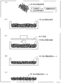
- the LED chip 151 is sealed by compression molding of a sealing resin 153 containing a phosphor 152, and the sealing resin 153 is further compression molded of a transparent sealing resin 154.
- Two-stage sealing type Patent Document 1.
- a sedimentation type in which an LED chip is sealed by compression molding of a sealing resin containing a phosphor, and the phosphor in the sealing resin is sedimented and distributed in the vicinity of the LED chip (Patent Document 2).
- the resin for compression molding (mostly silicone) has a higher viscosity than the resin for transfer potting, so the phosphor is difficult to settle, and the compression molding is short in the curing time of the resin, so before the phosphor settles This is because the resin hardens.
- the LED chip 161 is sealed by compression formation of a transparent sealing resin 162, and the transparent covering resin 162 is covered with a resin sheet 164 containing a phosphor 163. type.
- Patent Document 3 the LED chip connected on the substrate is covered with a thermosetting film (epoxy resin composition), and the thermosetting film is thermoset and sealed.
- Technology to stop is proposed.
- Patent Document 4 discloses a seal having an outermost resin layer (polycarbodiimide or the like), a light diffusion layer (polycarbodiimide or the like) containing light diffusing particles, and a resin layer (epoxy resin or the like) having a low refractive index.
- a stop sheet is laminated on a printed circuit board on which an optical semiconductor element is mounted with a vacuum laminator and press-molded with a stamper.
- Patent Document 5 discloses a technique of forming a liquid silicone mixed with a phosphor into a semi-cured sheet. According to the technique disclosed in Patent Document 5, liquid silicone mixed with a phosphor is molded into a semi-cured sheet, thereby improving the handling of the silicone and changing the viscosity depending on the surrounding environment. Is suppressed.
- the present invention has been made in view of the above problems, and its purpose is to equalize the concentration of the phosphor between the light emitting devices and to reduce the chromaticity value variation caused by the phosphor concentration and the phosphor content.
- An object of the present invention is to provide a method for manufacturing a light emitting device that can be reduced.
- a method for manufacturing a light-emitting device has a mounting step of mounting at least one light-emitting element on a substrate, and an upper surface of the light-emitting element mounted in the mounting step.
- An arrangement step of arranging a sealing material including at least a silicone resin that has been semi-cured by primary crosslinking and a phosphor at a position, and the sealing material arranged in the arrangement step are subjected to primary crosslinking.
- the silicone resin is heated at a temperature lower than the secondary crosslinking temperature, which is a temperature at which the silicone resin is completely cured by secondary crosslinking, and the sealing material melted in the melting step is melted in the melting step.
- a sealing material including at least a silicone resin that has been semi-cured by primary crosslinking and a phosphor is disposed at a position facing the upper surface of the light-emitting element mounted on the substrate.
- the silicone resin has a viscosity that reversibly decreases in a temperature range from room temperature to less than the secondary cross-linking temperature, and is irreversibly fully cured in a temperature range higher than the secondary cross-linking temperature. Therefore, the viscosity of the silicone resin can be repeatedly controlled by changing the temperature in the temperature range from room temperature to less than the secondary crosslinking temperature.
- the phosphor when the phosphor is kneaded into this silicone resin, the phosphor is uniformly dispersed in the silicone resin by controlling (lowering) the viscosity of the silicone resin so that the kneaded phosphor does not settle. It becomes possible.
- a sealing material in which the phosphor is uniformly dispersed in the silicone resin can be obtained. Therefore, by sealing the light emitting element using this sealing material, It is possible to realize a method for manufacturing a light-emitting device that can equalize the phosphor concentrations and reduce variations in chromaticity values due to the phosphor concentration and phosphor content.
- the method for manufacturing a light emitting device includes a mounting step of mounting at least one light emitting element on a substrate, and a position facing the upper surface of the light emitting element mounted in the mounting step.
- An arrangement step of arranging a sealing material including a silicone resin that has become semi-cured by primary crosslinking and a phosphor, and the sealing material arranged in the arrangement step are obtained by secondary crosslinking of the silicone resin.
- a method for manufacturing a light emitting device capable of equalizing the phosphor concentration between the light emitting devices and reducing variations in chromaticity values due to the phosphor concentration and the phosphor content. There is an effect that it can be provided.
- FIG. 1 is a perspective view showing an external configuration of a light emitting device manufactured by the method for manufacturing a light emitting device according to Embodiment 1.
- FIG. FIGS. 2A to 2D are schematic views showing a process of mounting the light emitting element in the cavity, out of the manufacturing processes of the light emitting device shown in FIG.
- FIGS. 3A to 3C are schematic views showing a process of sealing the inside of the cavity with a sealing resin in the manufacturing process of the light emitting device shown in FIG.
- FIG. 4 is a graph showing the viscosity characteristics of the silicone resin constituting the sealing resin sheet shown in FIG. 5 (a) to 5 (d) are graphs for explaining the viscosity state of the silicone resin in the step shown in FIG. 3 (b).
- FIG. 6 (a) to 6 (c) are schematic views showing the state of the sealing resin sheet in the vacuum heating furnace shown in FIG. 3 (b).
- FIG. 7 is a schematic view showing a step of dividing the multi-cavity circuit board shown in FIG. 3C among the manufacturing steps of the light emitting device shown in FIG.
- FIG. 8 is a table showing various data related to the method for manufacturing the light emitting device according to the first embodiment.
- 9 (a) to 9 (e) are schematic views showing a method for producing the encapsulating resin sheet shown in FIG. 3 (a).
- 10 (a) and 10 (b) are graphs for explaining the viscosity state of the silicone resin in the steps shown in FIGS. 9 (a) to 9 (e).
- FIG. 11 is a cross-sectional view showing another method for forming the kneaded resin shown in FIG. 9C into a sheet.
- 12 is a cross-sectional view showing an internal structure of a vacuum heating apparatus that can be used for manufacturing the light-emitting device shown in FIG.
- FIGS. 13A to 13C are schematic views showing steps of a vacuum heating method applicable to the method for manufacturing a light emitting device.
- 14 (a) to 14 (c) are schematic views showing a cavity in which a pair of through holes are formed at the bottom, and FIG. 14 (a) is a longitudinal sectional view of the cavity.
- 14 (b) is a plan view of the cavity shown in FIG. 14 (a), and
- FIG. 14 (c) is a cross-sectional view of the cavity shown in FIG.
- 15A is a cross-sectional view showing a cavity in which one through hole is formed in the bottom
- FIG. 15B is a cross-sectional view showing a sealing resin sheet in which the through hole is formed.
- FIGS. 16A to 16C are schematic views showing a method for manufacturing a light emitting device for sealing a light emitting element by stacking two sealing resin sheets each having a different phosphor content. is there.
- FIGS. 17A to 17C are schematic views illustrating a method for manufacturing a light-emitting device having a rod lens.
- FIG. 18 is a cross-sectional view showing a pressed state in the vacuum hot press apparatus shown in FIG. FIG.
- FIG. 19A is a perspective view showing a multiple cavity circuit board on which a rod lens is formed
- FIG. 19B is a view of dividing the multiple cavity circuit board shown in FIG. It is a perspective view which shows the light-emitting device obtained in this way
- 20A is a perspective view showing a multiple cavity circuit board on which a convex lens is formed
- FIG. 20B is a diagram obtained by dividing the multiple cavity circuit board shown in FIG. It is a perspective view which shows the obtained light emitting device.
- FIG. 21A to FIG. 21E are schematic views showing a process of mounting a light emitting element on a planar circuit board in the manufacturing process of the light emitting device according to the second embodiment.
- FIG. 21A to FIG. 21E are schematic views showing a process of mounting a light emitting element on a planar circuit board in the manufacturing process of the light emitting device according to the second embodiment.
- FIG. 21A to FIG. 21E are schematic views showing a process of mounting a light emitting element on
- FIG. 22 is a cross-sectional view showing a pressure press state in a vacuum hot press apparatus.
- FIG. 23A is a perspective view of the planar circuit board after pressure pressing shown in FIG. 22, and
- FIG. 23B is a plan view of the planar circuit board shown in FIG. It is a perspective view which shows the light-emitting device obtained in this way.
- 24A is a plan view showing an example of a dot matrix type light emitting display device
- FIG. 24B is a cross-sectional view of the light emitting display device shown in FIG.
- FIG. 25 is a schematic view showing an example of a method for manufacturing the light-emitting device shown in FIG. 24 (a) and FIG. 24 (b).
- FIG. 26 is a cross-sectional view showing a pressure press state in the vacuum hot press apparatus.
- FIGS. 27A to 27C are schematic views showing a method for manufacturing a single optical device.
- FIGS. 28A to 28D are schematic views showing a method for manufacturing the light emitting device according to the third embodiment.
- FIG. 29 is a table showing various data related to the method for manufacturing the light emitting device according to the third embodiment.
- FIG. 30 is a schematic view showing a manufacturing process of a sealing resin powder that is a silicone resin powder including a phosphor.
- FIG. 31 (a) to FIG. 31 (c) are schematic views showing a method for manufacturing a light emitting device using a sealing resin tablet.
- 32 (a) to 32 (e) are schematic views showing a method for producing a mixed powder sheet for sealing, in which the mixed powder for sealing shown in FIG. 28 (a) is formed into a sheet. It is sectional drawing which shows the structure of the conventional light-emitting device. It is sectional drawing which shows the flow of the manufacturing method of the conventional light-emitting device.
- Embodiment 1 An embodiment relating to a method for manufacturing a light emitting device according to the present invention will be described below with reference to FIGS.
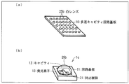
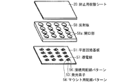
- FIG. 1 is a perspective view showing an external configuration of a light emitting device 1a manufactured by the method for manufacturing a light emitting device according to the present embodiment.
- a light-emitting device 1a includes a rectangular parallelepiped cavity that opens upward on a circuit board (substrate) 11 that is a rectangular parallelepiped MID (Molded Interconnection Device) having a side of about 1 mm. 12 is formed, and a light emitting element 13 such as an LED is mounted in the cavity 12.
- a circuit board (substrate) 11 that is a rectangular parallelepiped MID (Molded Interconnection Device) having a side of about 1 mm. 12 is formed, and a light emitting element 13 such as an LED is mounted in the cavity 12.
- the lower surface of the light emitting element 13 is connected to a mounting wiring pattern 14 provided at the bottom of the cavity 12 by a conductive adhesive 15 (die bonding). Further, the upper surface of the light emitting element 13 is connected to a connection wiring pattern 16 provided at the bottom of the cavity 12 by a conductive wire 17 constituted by a gold wire or the like (wire bonding).
- the inside of the cavity 12 of the circuit board 11 is sealed with a sealing resin 21 made of a light-transmitting silicone resin.
- the method for mounting the light emitting element 13 on the circuit board 11 is not particularly limited, and the light emitting element 13 may be mounted on the circuit board 11 by, for example, a flip chip method instead of the wire bonding method.
- FIG. 2 (a) to 2 (d) are schematic diagrams showing a process of mounting the light emitting element 13 in the cavity 12 in the manufacturing process of the light emitting device 1a shown in FIG.
- a multiple cavity circuit board 10 in which a large number of cavities 12 are formed in a matrix in the vertical and horizontal directions is used.
- the multi-cavity circuit board 10 has a thickness of 1.0 mm, for example, and the depth of each cavity 12 is 0.6 mm.
- a mounting wiring pattern 14 and a connecting wiring pattern 16 are provided at the bottom of each cavity 12, respectively.
- a conductive adhesive 15 is applied on the wiring pattern 14 for mounting provided on the bottom of each cavity 12 of the multiple cavity circuit board 10.
- the light emitting element 13 is die-bonded on the conductive adhesive 15 applied on the mounting wiring pattern 14. Further, as shown in FIG. 2D, the upper surface of the light emitting element 13 and the connection wiring pattern 16 provided at the bottom of the cavity 12 are wire-bonded by a conductive wire 17 constituted by a gold wire or the like.
- each cavity 12 is filled with a silicone resin containing a phosphor. Seal.
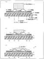
- FIGS. 3A to 3C are schematic views showing a process of sealing the inside of the cavity 12 with the sealing resin 21 in the manufacturing process of the light emitting device 1a shown in FIG. 4 is a graph showing the viscosity characteristics of the silicone resin constituting the sealing resin sheet (sealing material) 20 shown in FIG. 3 (a).
- FIG. 5 (a) to FIG. 5 (d) These are the graphs which show the viscosity state of the silicone resin in the process shown by (b) of FIG.
- the viscosity characteristic of the silicone resin is shown to change linearly for convenience, but the viscosity characteristic of the silicone resin is not necessarily linear. It is not limited to things that change.
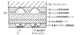
- a sealing resin sheet 20 and a surface molding release sheet (film) 31 are formed on the multiple cavity circuit board 10 in which the light emitting element 13 is mounted in each cavity 12. And the weight plate 32 are laminated in this order.
- a sealing resin sheet 20 is used to simultaneously seal the inside of each cavity 12 with a sealing resin 21 containing a phosphor.
- the sealing resin sheet 20 is obtained by dispersing a phosphor in a thermoplastic silicone resin.
- This silicone resin is in a semi-cured state due to the formation of primary crosslinks and has a predetermined viscosity.
- the semi-cured state (B-STAGE) is between the uncured state (A-STAGE) and the fully cured state (C-STAGE), and is more than the uncured state by primary crosslinking. It means a state having a high viscosity.
- this silicone resin has a viscosity V 0 of the silicone resin at room temperature T 0 (see P 0 in the figure).
- the viscosity V 0 is, for example, a viscosity that allows the silicone resin to maintain a sheet shape so that the sealing resin sheet 20 can be easily handled at room temperature T 0 .
- the change in the viscosity of the silicone resin in the temperature range from room temperature T 0 to less than the secondary crosslinking temperature T 1 is due to the polymer chain in the silicone resin being entangled or unwound by Brownian motion, and is a thermoreversible change. It is. Therefore, when the temperature is lowered from the vicinity of the secondary crosslinking temperature T 1 to the room temperature T 0 , the viscosity of the silicone resin increases and returns to the original viscosity V 0 at the room temperature T 0 . Therefore, the viscosity of the silicone resin can be repeatedly controlled between the viscosity V 0 and the viscosity V 1 by changing the temperature in the temperature range from room temperature T 0 to less than the secondary crosslinking temperature T 1 .
- the viscosity of the silicone resin is increased from the viscosity V 1 to a viscosity V 2 (see figure P 2) .
- the viscosity V 2 is the viscosity when the silicone resin is completely cured.
- Viscosity change of the silicone resin in the secondary crosslinking temperature T 1 of is a thermal irreversible change. Therefore, even when the temperature is lowered from the secondary crosslinking temperature T 1 to the room temperature T 0 , the viscosity of the silicone resin does not change and maintains the fully cured state (see P 3 in the figure).
- the sealing resin sheet 20 in which the phosphor is uniformly dispersed can be formed as described later.
- sealing resin sheet 20 for example, a trade name “TX-2506 series” manufactured by Dow Corning can be suitably used.
- the sealing resin sheet 20 is formed in a size substantially the same as that of the multiple cavity circuit board 10 so as to cover all the cavities 12 formed in the multiple cavity circuit board 10. Further, it is preferable that the cavity 12 is formed to a thickness of about 0.2 mm to 0.4 mm, which is smaller than the depth (0.6 mm) of each cavity 12.
- the surface molding release sheet 31 laminated on the sealing resin sheet 20 has a satin finish on the surface in contact with the sealing resin sheet 20 in order to finish the surface of the sealing resin 21 in a satin finish. .
- this surface forming release sheet 31 the light extraction efficiency of the light emitting device 1a can be improved.
- the surface shape of the weight plate (mold) 32 may be changed.
- the multiple cavity circuit board 10 the sealing resin sheet 20, the surface forming release sheet 31, and the weight plate 32 are stacked in a vacuum. It is set in the heating furnace 33 and heated to melt (melting step).
- the sealing resin sheet 20 is heated from room temperature T 0 to a temperature T 4 in the vicinity of the secondary crosslinking temperature T 1 (for example, 80 ° C. or higher and lower than 120 ° C.). As a result, the viscosity of the silicone resin is reduced to a flowable viscosity V 4 (see P 4 in the figure).
- the vacuum heating furnace 33 is configured to heat the inside with a vacuum state, and the sealing resin sheet 20 and the surface molding release sheet 31 on the multiple cavity circuit board 10 placed in a vacuum state are In combination with the pressing action by the weight plate 32, the heating is performed in a state of being in close contact with each other. Therefore, since the molten silicone resin flows into each cavity 12, the molten silicone resin can be filled in each cavity 12. At this time, the molten silicone resin remaining on the surface of the multiple cavity circuit board 10 between the cavities 12 also flows into the cavities 12. Therefore, as described above, even if the thickness of the sealing resin sheet 20 is made thinner than the depth of the cavity 12 (approximately about 3/5 of the depth of the cavity 12), it melts in each cavity 12. The silicone resin will be almost full.
- the sealing resin sheet 20 may be made thicker. However, in this case, a large amount of silicone resin and phosphor that overflow from the periphery of the weight plate 32 and are not used for sealing the cavity 12 are generated. Since the silicone resin and the phosphor overflowing from the periphery of the weight plate 32 cannot be reused and must be discarded, when considering the material cost of the silicone resin and the phosphor, the sealing resin as described above It is preferable to set the sheet 20 thinner than the depth of the cavity 12.
- the temperature T 4 from a secondary crosslinking temperature T 1 (for example, 120 ° C. or higher 170 ° C. or less) for heating the sealing resin sheet 20 at a temperature of (FIG. referring to the medium P 1).
- a secondary crosslinking temperature T 1 for example, 120 ° C. or higher 170 ° C. or less
- T 1 for example, 120 ° C. or higher 170 ° C. or less
- the weight plate 32 and the surface forming release sheet 31 are sequentially removed from the multiple cavity circuit board 10. Thereby, the light emitting element 13 in each cavity 12 is in a state in which the surface is finished in a satin finish and is sealed with the sealing resin 21.
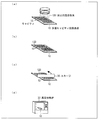
- FIG. 6 (a) to 6 (c) are schematic views showing the state of the sealing resin sheet 20 in the vacuum heating furnace 33 shown in FIG. 3 (b).
- the sealing resin sheet 20 when set in the vacuum heating furnace 33, while holding the sheet form at room temperature T 0, is heated by a vacuum heating furnace 33
- the viscosity of the sealing resin sheet 20 is lowered to be in a curved state. Then, the silicone resin is melted by further heating to about 100 ° C. and flows into the cavities 12 as shown in FIG.
- the sealing resin sheet 20 is pressed by the weight plate 32, the melted silicone resin is uniformly filled into the cavities 12 by the pulling of the silicone resin. In the present embodiment, it takes about 30 minutes to fill each cavity 12 with the molten silicone resin.
- the multiple cavity circuit board 10 is 150 ° C. in a state of being accommodated in the vacuum heating furnace 33. Heat to the extent.
- the molten silicone resin to further viscosity until it reaches the secondary crosslinking temperature T 1 is in a state of reduced, remaining on the surface of the multiple-cavity circuit board 10 between the cavities 12 Molten silicone resin flows into each adjacent cavity 12. Thereby, the molten silicone resin does not remain on the surface of the multiple cavity circuit board 10. Therefore, even if the sealing resin sheet 20 is molded with a thickness smaller than the depth of each cavity 12, the melted silicone resin is almost completely filled in each cavity 12.
- the silicone resin filled in each cavity 12 is fully cured by secondary crosslinking by being heated to a high temperature of 150 ° C. by the vacuum heating furnace 33. In the present embodiment, a heating time of about 30 minutes is required until the molten silicone resin in each cavity 12 is secondarily crosslinked and fully cured.
- the sealing resin sheet 20 by melting the sealing resin sheet 20 in a state where the surface of the surface forming release sheet 31 is in close contact, the melted silicone resin can be filled in each cavity 12. Thereafter, the sealing resin 21 can be formed by heating the molten silicone resin to the secondary crosslinking temperature.
- FIG. 7 is a schematic view showing a step of dividing the multi-cavity circuit board 10 shown in FIG. 3C among the manufacturing steps of the light emitting device 1a shown in FIG. As shown in FIG. 7, when the light emitting element 13 in each cavity 12 is sealed with the sealing resin 21, the multiple cavity circuit board 10 is divided into each cavity 12 (division step). Thereby, many light emitting devices 1a in which the surface of the sealing resin 21 has a satin finish can be obtained.
- the circuit configuration has a plurality of cavities 12 in which the light emitting elements 13 in each cavity 12 are electrically connected. Since the multiple cavity circuit board 10 is divided, a dot matrix type light emitting device in which a large number of light emitting elements 13 are arranged in a matrix can be obtained.
- the sealing resin sheet 20 stacked on the multiple cavity circuit board 10 has a thickness of about 0.2 mm to 0.4 mm, whereas the depth of the cavity 12 is 0.6 mm. Molded. If the sealing resin sheet 20 becomes too thick, after the curing step is completed, the molten silicone resin remains on the surface between the cavities 12 in the multiple cavity circuit board 10. When the silicone resin remaining on the surface of the multiple cavity circuit board 10 is cured, the light emitted from the light emitting element 13 may be scattered by the remaining silicone resin. Therefore, the sealing resin sheet 20 is preferably thinner than the depth of the cavity 12.
- FIG. 8 is a table showing various data related to the manufacturing method of the light emitting device according to the present embodiment.
- FIG. 8 also shows data by a conventional casting sealing method as a comparative example.
- the casting sealing method shown in FIG. 8 uses a general silicone resin in which the initial state used in the past is liquid as described in the above-mentioned problem to be solved by the present invention.
- the silicone resin according to the present invention having the viscosity characteristics shown in FIG. 4 is not used (see FIG. 34).
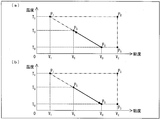
- each manufactured light emitting device 1a has a chromaticity distribution width of 3 ranks, and the light emitting device (15) manufactured by the conventional casting sealing method. Compared to (Rank), variation in chromaticity values (range of chromaticity distribution) between the light emitting devices 1a can be reduced.
- the values of X and Y in the column of chromaticity distribution width shown in FIG. 8 are classified into predetermined ranges when the chromaticity values of light-emitting devices mass-produced by the respective methods are plotted on the CIE1931 chromaticity diagram.
- the rank (division) value indicates the number of ranks (divisions) that the chromaticity distribution of the mass-produced light emitting devices spans, and the variation in chromaticity values is a plurality of adjacent frames (chromaticity ranks). It shows that it is distributed across.
- the variation range of the chromaticity values between the light emitting devices 1a can be reduced. As described above, this is the content of the phosphor contained in each light emitting device 1a. This is because it is possible to equalize almost the same amount.
- the light emitting device 1a manufactured by the sheet resin method of the present embodiment has smaller values of X and Y and rank (division) values than the light emitting device manufactured by the conventional casting sealing method. It can be seen that the variation in chromaticity values among the light-emitting devices 1a that are mass-produced is very small.
- the head of the conventional casting sealing method in the column of production efficiency / mold time shown in FIG. 8 indicates the number of dispenser heads of the phosphor coating device used for casting. It shows that the phosphor layer can be simultaneously applied (casting sealing).
- the time indicates the time required for applying the phosphor layer (casting sealing) (that is, equivalent to the molding time). When this is converted into the time per cavity 12 (light emitting device 1a), it becomes 0.17 sec / pcts in the case of 6 heads.
- the tact of the sheet resin method of the present embodiment indicates the time of the vacuum hot pressing process of the sheet resin (that is, equivalent to the molding time).
- the tact of the sheet resin method of the present embodiment indicates the time of the vacuum hot pressing process of the sheet resin (that is, equivalent to the molding time).
- the production time is improved because the molding time is shortened compared to the conventional casting sealing method.
- the number of copies in the column of waste resin / phosphor amount shown in FIG. 8 is that 100 light-emitting devices are manufactured when the amount of silicone resin and phosphor contained in the sealing resin 21 of one light-emitting device is 1 part. (That is, when 100 parts of the sealing resin 21 is formed), the amount of discarded resin / phosphor generated in the manufacturing process is quantitatively shown. According to the sheet resin method according to the present embodiment, only the silicone resin and the phosphor overflowing from the periphery of the weight plate 32 in the vacuum hot press process become the amount of waste resin / phosphor.
- the phosphor concentration in the casting machine changes with time due to sedimentation of the phosphor in the casting machine (dispenser). All of the contained resin cannot be used up (usually discarded in about half), and the amount of waste resin / phosphor increases.
- each cavity is filled with a silicone resin at the same time, so that the production efficiency can be improved and the amount of resin and phosphor discarded in the manufacturing process can be reduced. .
- FIG. 9 (a) to FIG. 9 (e) are schematic views showing a manufacturing method of the sealing resin sheet 20 shown in FIG. 3 (a).
- FIG. 10 (a) and FIG. FIG. 9B is a graph for explaining the viscosity state of the silicone resin in the steps shown in FIGS. 9A to 9E.
- the viscosity characteristic of the silicone resin is shown to change linearly, but the viscosity characteristic of the silicone resin does not necessarily change linearly. Not limited to.
- the silicone resin 22 shown in FIG. 9 (a) has a primary crosslink, and the amount of the solvent of the semi-cured material diluted with BTX (benzene, toluene, xylene) or the like is appropriately reduced. It was obtained by removing.
- BTX benzene, toluene, xylene
- the silicone resin 22 is heated from a room temperature T 0 to a temperature temperature T 5 (for example, 40 or more and less than 60 ° C.).
- T 5 for example, 40 or more and less than 60 ° C.
- the viscosity is reduced to a viscosity V 5 that allows the kneaded phosphor not to settle (see P 5 in the figure).
- the phosphor and the silicone resin 22 measured in a predetermined amount are put in a container and stirred until the dispersed state of the phosphor in the silicone resin 22 becomes uniform. Knead by doing. As a result, as shown in FIG. 9C, a kneaded resin 24, which is a silicone resin 22 in which the phosphor is uniformly dispersed, is obtained.
- a general kneading apparatus such as a ball mill using a high hardness material or a (heating vacuum) kneader can be used.
- a heating mechanism temperature adjustment mechanism
- ball mills and kneaders are decompressed by a vacuum device.
- the phosphor does not settle the viscosity of the silicone resin 22 after the primary crosslinking. Since it can be adjusted as appropriate, the dispersion state of the phosphor in the silicone resin 22 can be adjusted.
- the phosphor and the silicone resin 22 can be kneaded without significantly reducing the viscosity of the silicone resin 22. Therefore, it is possible to suppress the phosphor from being biased in the silicone resin 22 and to improve the uniform dispersibility of the phosphor in the silicone resin 22.
- the shape of the silicone resin 22 kneaded with the phosphor is not necessarily a sheet shape, but it is appropriately reworked from the obtained shape to seal the desired LED package.
- a sealing (starting) member shape for stopping may be used.
- the form of the primary crosslinked silicone resin 22 to be introduced into the kneading apparatus is not limited to a resinous form having a reduced viscosity.
- the shape may be a shape. That is, a sample for obtaining a sealing resin form (secondary processed product) optimal for sealing processing using the kneading apparatus after dry blending the phosphor and the powder of the silicone resin 22 in advance ( Primary processed product) may be manufactured (a primary processed product may be obtained from a dry blend product).
- the kneading apparatus includes the above-described heating mechanism, so that the particles of the silicone resin 22 that have been heated and melted are combined and kneaded while entraining the phosphor.
- the manufacturing method of the light emitting device using the powdery silicone resin 22 will be described later.
- the solvent remaining in the silicone resin 22 is removed under reduced pressure during the phosphor kneading process, or is removed by drying when the kneaded resin 24 is formed into a sheet.
- the method for forming the kneaded resin 24 into a sheet is not limited to the press method described above, and various melting methods such as a T-die method, a calender roll method, and a doctor blade method can be used.
- FIG. 11 is a cross-sectional view showing another method for forming the kneaded resin 24 shown in FIG. 9C into a sheet.
- FIG. 11 shows a process of forming the kneaded resin 24 into a sheet by the T-die method.
- the mold 131 to which the nozzle 132 having the opening 132a opened with a certain width is attached is roughly roughened to a predetermined size.
- the pulverized kneaded resin 24 is disposed. Then, by pressing the kneaded resin 24 with the pressurizing member 139, the kneaded resin 24 can be formed into a sheet in the width of the opening 132a.
- the width of the opening 132a is appropriately changed according to the required thickness of the sealing resin sheet 20.
- the phosphor when the phosphor is kneaded with this silicone resin, the phosphor can be uniformly dispersed in the silicone resin by controlling the viscosity of the silicone resin so that the kneaded phosphor does not settle. Therefore, the sealing resin sheet 20 in which the phosphor is uniformly dispersed can be obtained.
- each light emitting element 13 can be sealed by bringing the phosphor concentration (phosphor content) in each cavity 12 into a substantially uniform state by closely adhering to the side surface and fully curing by secondary crosslinking in this state. .
- the melted silicone resin is added to each cavity without using a special dispenser or molding machine for filling the melted silicone resin into each cavity 12. 12 can be filled simultaneously, so that the production efficiency of the light emitting device 1a can be remarkably improved.
- the phosphor concentration between the light emitting devices 1a is equalized, and the manufacture of the light emitting device capable of reducing variations in chromaticity values due to the phosphor concentration and phosphor content.
- a method can be realized.
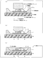
- Modification 1 In the present embodiment, the vacuum heating furnace in a state where the multiple cavity circuit board 10 on which the light emitting element 13 is mounted, the sealing resin sheet 20, the surface molding release sheet 31, and the weight plate 32 are stacked. Although the method of heating in a vacuum state by 33 has been described, a method in which the weight plate 32 is not used may be used.
- FIG. 12 is a cross-sectional view showing the internal structure of the vacuum heating apparatus 40 that can be used for manufacturing the light emitting device 1a shown in FIG.
- a vacuum heating device (trade name “vacuum laminator”, manufactured by NPC Corporation) that can be heated while being pressurized in a vacuum state without using the weight plate 32 is used in a series.
- the cavity circuit board 10, the sealing resin sheet 20, and the surface molding release sheet 31 may be heated in a stacked state.
- the upper chamber 41 and the lower chamber 42 are separated from each other by a diaphragm rubber 43, and the upper chamber 41 and the lower chamber 42 are each in a vacuum state.
- a hot plate 44 is disposed in the lower chamber 42, and the multiple cavity circuit board 10 is mounted on the hot plate 44 in a state where the sealing resin sheet 20 and the surface molding release sheet 31 are laminated. Placed.
- the multiple cavity circuit board 10 When the multiple cavity circuit board 10 is placed on the hot plate 44 in a state where the sealing resin sheet 20 and the surface molding release sheet 31 are laminated, the inside of the upper chamber 41 and the lower chamber 42 are evacuated. At the same time, the hot plate 44 is heated to melt the sealing resin sheet 20.
- the surface molding release sheet 31 is pressed against the surface of the melted silicone resin filled in each cavity 12 of the multiple cavity circuit board 10 by the vacuum rubber action and the vacuum action.
- the surface of the fully cured silicone resin can be formed into a satin finish without bubbles being mixed into the silicone resin. Even in this case, by controlling the temperature of the hot plate 44, the vacuum resin heating device 40 performs the operation until the silicone resin is melted and filled in each cavity 12, and is fully cured by secondary crosslinking. be able to.
- FIGS. 13A to 13C are schematic views showing the steps of a vacuum heating method applicable to the method for manufacturing a light emitting device.
- the vacuuming bag 38a connected to the vacuum pump 38d can be used for manufacturing the light emitting device 1a.
- one end of the tube 38b is connected in an airtight state to the opening of the vacuuming bag 38a, and then, as shown in FIG. Alternatively, the bag 38a may be placed in the heating furnace 38c and heated while the vacuuming bag 38a is evacuated by the vacuum pump 38d.
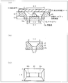
- the sealing resin sheet 20 is placed on the multiple-cavity circuit board 10 and heated. However, in this case, a pair of through holes 12a are formed at the bottom of each cavity 12. May be provided respectively.
- FIG. 14 (a) to 14 (c) are schematic views showing the cavity 12 having a pair of through holes 12a formed at the bottom, and FIG. 14 (a) is a longitudinal sectional view of the cavity 12.
- FIG. 14B is a cross-sectional view of the cavity 12 shown in FIG. 14A, and
- FIG. 14C is a plan view of the cavity 12 shown in FIG. .
- the size of the opening of each cavity 12 is a rectangle of 3.0 mm ⁇ 1.8 mm
- the size of the bottom of each cavity 12 is as follows. Is a rectangle of 2.2 mm ⁇ 0.6 mm, the depth of each cavity 12 is 0.7 mm, and the bottom portion of each cavity 12 protrudes downward by 0.4 mm corresponding to the length of the through hole 12a.
- a pair of rectangular through holes 12a of 0.4 mm ⁇ 0.6 mm are provided at each end in the longitudinal direction at the bottom of each cavity 12, with a spacing of 1.4 mm from each other. Open and form.
- a sheet or a plate having excellent releasability may be laid under the multiple cavity circuit board 10.
- the multiple cavity circuit board 10 can be easily taken out from the heating furnace or the like without being in close contact with the heating plate or the like. Can do.
- FIG. 15A is a cross-sectional view showing the cavity 12 in which one through hole 12a is formed in the bottom, and FIG. 15B shows the sealing resin sheet 20 in which the through hole 20a is formed. It is sectional drawing. As shown to (a) of FIG. 15, the through-hole 12a provided in the bottom part of each cavity 12 does not need to be a pair, and you may make it provide one through-hole 12a.
- the through hole 12 a is not limited to the bottom of each cavity 12, and may be provided on the side surface of the cavity 12. Further, the through hole 12a is not limited to a rectangular cross section, but may be a circular cross section, a triangular cross section, or the like.
- the through holes 20 a are respectively formed in the portions of the sealing resin sheet 20 facing the respective cavities 12. You may make it form. Also in this case, when the periphery of the multiple cavity circuit board 10 is in a vacuum state and the silicone resin of the sealing resin sheet 20 is melted, the through holes 20a provided in the sealing resin sheet 20 The air in each cavity 12 can be discharged. Therefore, it is possible to suppress the mixing of bubbles into the molten silicone resin filled in each cavity 12. In addition, the adhesion between the inner surface of each cavity 12 and the sealing resin 21 can be improved.
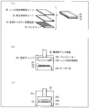
- Modification 3 In the present embodiment, the method of sealing the light emitting element 13 using one sealing resin sheet 20 has been described. However, the light emitting element 13 is formed by stacking a plurality of sealing resin sheets having different phosphor contents. May be sealed.
- FIG. 16 (a) to 16 (c) show a method for manufacturing a light-emitting device in which the light-emitting element 13 is sealed using two sealing resin sheets 20A and 20B having different phosphor contents.
- FIG. 16A the first sealing resin sheet 20 ⁇ / b> A and the second sealing resin sheet 20 ⁇ / b> B having different phosphor contents are used as the sealing resin sheet 20 to form multiple cavities. You may arrange
- the first sealing resin sheet 20A and the second sealing resin sheet 20B have the same size as the multiple cavity circuit board 10 so as to cover all the cavities 12, respectively,
- the sealing resin sheet 20 ⁇ / b> A is overlaid in a state aligned with the multiple cavity circuit board 10.
- the cavity circuit board 10 is set in the vacuum hot press device 35.
- a trade name “Vacuum Laminate Press” manufactured by Kitagawa Seiki Co., Ltd. is used for the vacuum hot press device 35.
- the vacuum heat press device 35 includes a heatable heater base 35a disposed in a vacuum chamber 35c, and a heatable press heater 35b that can be brought into and out of contact with the heater base 35a.
- the multiple cavity circuit board 10 in which the first sealing resin sheet 20A, the second sealing resin sheet 20B, and the surface molding release sheet 31 are stacked is set on the heater base 35a. . Then, with the multiple cavity circuit board 10 set on the heater base 35a, the inside of the vacuum chamber 35c is depressurized to 10 torr.
- the heated press heater 35b is lowered, and the multiple cavity circuit board 10 set on the heater base 35a is replaced with the first sealing resin sheet 20A.
- the second sealing resin sheet 20B is heated at about 100 ° C. while being pressurized at 20 kg / cm 2 .
- the lower heater base 35a is not heated. After performing the heat press by the press heater 35b, it further heats to about 150 degreeC.
- the first sealing resin sheet 20A and the second sealing resin sheet 20B are melted and melted in the cavities 12, respectively. And is fully cured by secondary crosslinking.
- the light emitting device can be obtained by dividing into cavities 12 or dividing into a predetermined number of cavities 12.
- the dispersion concentration of the phosphor in the cavity 12 can be easily controlled by superimposing the first sealing resin sheet 20A and the second sealing resin sheet 20B having different phosphor contents. can do.
- a vacuum impregnation apparatus may be used instead of the vacuum hot press apparatus 35.
- the vacuum impregnation apparatus when the melted silicone resin is filled in the cavity 12, the inside of the chamber is pressurized by increasing the pressure from normal pressure. According to this vacuum impregnation apparatus, the process of filling the cavity 12 with the melted silicone resin by heating under high pressure in the vacuum impregnation apparatus can be easily performed, so that the working efficiency can be improved. .
- Modification 4 In the present embodiment, the method of disposing the surface molding release sheet 31 on the sealing resin sheet 20 has been described. However, instead of the surface molding release sheet 31, a lens molding resin sheet 25 is disposed. Also good.
- FIG. 17 (a) to 17 (c) are schematic views showing a method of manufacturing a light emitting device having a rod lens
- FIG. 18 is a schematic view of the vacuum hot press apparatus 35 shown in FIG. 17 (c). It is sectional drawing which shows a press state.
- the sealing resin sheet 20 and the lens molding resin sheet 25 are stacked on the multiple cavity circuit board 10 as shown in FIG. And set in the vacuum hot press device 35.
- the lens molding resin sheet 25 is made of, for example, a high molecular weight unsaturated polyester resin.
- the depth of each cavity 12 formed in the multiple cavity circuit board 10 is 0.6 mm
- the thickness of the sealing resin sheet 20 is 0.5 mm
- the lens molding resin The thickness of the sheet 25 is 1.0 mm.
- a lens molding die 35d is attached to the lower side of the press heater 35b.
- a semi-cylindrical lens molding groove portion (molding concave portion: see FIG. 18) 35e having a radius of 0.9 mm is provided along the row of the cavities 12 in the multiple cavity circuit board 10. Are formed in parallel.
- the inside of the vacuum chamber 35c is reduced to 10 torr.
- the heated press heater 35b is lowered, and the sealing resin sheet 20 and the lens molding resin sheet 25 on the multiple cavity circuit board 10 are pressurized to 20 kg / Heating at about 100 ° C. while applying pressure at cm 2 . Accordingly, the sealing resin sheet 20 and the lens molding resin sheet 25 are in a molten state, and the melted silicone resin of the sealing resin sheet 20 is filled in each cavity 12, and the lens molding resin sheet 25. The molten lens molding resin is filled in the lens molding groove 35e.
- FIG. 19A is a perspective view showing a multiple cavity circuit board 10 on which rod lenses are formed
- FIG. 19B is a multiple cavity circuit board 10 shown in FIG. It is a perspective view which shows the light-emitting device 1b obtained by dividing
- the silicone resin filled in each cavity 12 and the lens molding resin filled in the lens molding groove 35e are cured, so that the multiple cavity circuit board 10 is formed.
- a plurality of semi-cylindrical rod lenses 25a can be formed.
- the light emitting elements 13 mounted in the cavities 12 of the circuit board 11 are sealed with a sealing resin 21 as shown in FIG. Furthermore, the light emitting device 1b in which the semi-cylindrical rod lens 25a is provided on the sealing resin 21 can be obtained.
- the lens molding die 35d when the lens lens 25a is molded by the lens molding die 35d after melting the lens molding resin sheet 25, bubbles are prevented from being mixed into the melted lens molding resin.
- the lens molding die 35d does not need to be attached to the press heater 35b, and may be used in a state of being placed on the lens molding resin sheet 25.
- the lens formed on the sealing resin 21 is not limited to the semi-cylindrical rod lens 25a, and a hemispherical convex lens 25b may be formed.
- FIG. 20A is a perspective view showing a multiple cavity circuit board 10 on which a convex lens is formed
- FIG. 20B shows the multiple cavity circuit board 10 shown in FIG. 20A. It is a perspective view which shows the light-emitting device 1c obtained by dividing
- a hemispherical convex lens 25b can be provided on each cavity 12 of the multiple cavity circuit board 10.
- a lens molding die 35d having a plurality of hemispherical lens molding recesses 35f (see FIG. 22) having a radius of 0.9 mm is used instead of the semi-cylindrical lens molding groove 35e.
- a lens molding die 35d having a plurality of hemispherical lens molding recesses 35f (see FIG. 22) having a radius of 0.9 mm is used.
- the hemispherical convex lens 25b can be formed.
- the multi-cavity circuit board 10 is divided into the cavities 12 so that the light emitting elements 13 mounted in the cavities 12 of the circuit board 11 are sealed with the sealing resin 21 as shown in FIG. Further, the light emitting device 1c in which the hemispherical convex lens 25b is provided on the sealing resin 21 can be obtained.
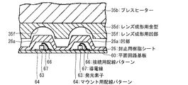
- the light emitting device manufacturing method according to the present embodiment is the same as the light emitting device manufacturing method according to the first embodiment in that a planar circuit board 60 having a flat surface is used instead of the multiple cavity circuit board 10. Mainly different.
- 21 (a) to 21 (e) are schematic diagrams showing a process of mounting a light emitting element on the planar circuit board 60 in the manufacturing process of the light emitting device according to the present embodiment.
- a pair of mounting wiring patterns 64 and connection wiring patterns 66 are arranged in a matrix in the vertical and horizontal directions on a planar circuit board 60 having a flat surface.
- a conductive adhesive 65 is applied on the mounting wiring pattern 64 provided on the planar circuit board 60.
- the light emitting element 63 is die-bonded on the conductive adhesive 65. Further, as shown in FIG. 21 (d), the upper surface of the light emitting element 63 and the connection wiring pattern 66 paired with the mounting wiring pattern 64 on which the light emitting element 63 is mounted are configured by gold wires or the like. Wire bonding is performed by the conductive wire 67.
- the mounting wiring pattern 64 and the connection wiring is placed on the planar circuit board 60 in an overlapping manner (placement step).
- a pair of mounting wiring patterns 64 and connection wiring patterns 66 provided on the planar circuit board 60 are accommodated in the respective recesses 26 a so as not to contact the light emitting elements 63 and the conductive wires 67. As shown, it is disposed on the planar circuit board 60 (see FIG. 22). Further, a convex portion corresponding to the concave portion 26 a is formed on the upper surface of the sealing resin sheet 26, whereby the thickness of the sealing resin sheet 26 is kept substantially constant.
- This sealing resin sheet 26 is made of a silicone resin having the viscosity characteristics shown in FIG. 4 and is obtained by kneading a phosphor into a semi-cured silicone resin obtained by primary crosslinking.
- FIG. 22 is a cross-sectional view showing a pressurized state in the vacuum hot press apparatus 35. As shown in FIG. 22, in this embodiment, a lens molding die 35d having a plurality of hemispherical lens molding recesses 35f is attached below the press heater 35b.
- the planar circuit board 60 is set on the heater base 35a in the vacuum hot press apparatus 35, and the inside of the vacuum chamber is decompressed to 10 torr. In such a state, the heated press heater 35b is lowered, and the planar circuit board 60 set on the heater base 35a is placed at 20 kg / cm 2 in a state where the sealing resin sheet 26 is overlaid. Heat at about 100 ° C. while applying pressure. Thereby, the silicone resin of the sealing resin sheet 26 can be melted and filled in the lens molding recess 35f of the lens molding die 35d. Furthermore, by heating to about 150 ° C., the silicone resin filled in the lens molding recess 35f can be fully cured by secondary crosslinking.
- the decompressed state in the vacuum chamber 35c is released, and the inside of the vacuum chamber 35c is returned to normal pressure. Thereafter, the press heater 35b is raised, and the vacuum hot press process by the vacuum hot press device 35 is finished.
- FIG. 23A is a perspective view of the planar circuit board 60 after the press pressing shown in FIG. 22, and FIG. 23B shows the planar circuit board 60 shown in FIG. It is a perspective view which shows the light-emitting device 1d obtained by dividing
- each light emitting element 63 is sealed with the hemispherical sealing resin 21 on the planar circuit board 60 after the vacuum hot pressing process is completed.
- the light emitting element 63 mounted on the circuit board 61 is sealed with a convex lens type sealing resin 21, as shown in FIG.
- the light emitting device 1d can be obtained.
- the method for manufacturing a light emitting device includes a mounting step of mounting a plurality of light emitting elements 13 on a planar circuit board 60 having a flat surface, and a plurality of light emitting elements 63 that can be mounted.
- the sealing resin sheet 26 used in the method for manufacturing a light emitting device according to the present embodiment is made of a silicone resin having a viscosity characteristic shown in FIG.
- the phosphor is uniformly dispersed.
- Modification 1 In the present embodiment, the method for manufacturing the light emitting device 1d sealed with the convex lens type sealing resin 21 has been described. However, the dot matrix type light emitting display device 50 is formed using the method for manufacturing the light emitting device according to the present invention. It can also be manufactured.
- FIG. 24A is a plan view showing an example of a dot matrix type light emitting display device 50
- FIG. 24B is a cross-sectional view of the light emitting display device 50 shown in FIG.
- the light-emitting display device 50 includes a pair of mounting wiring patterns 54 and connection wiring patterns 56 on a planar circuit board 51 in a vertical direction and a horizontal direction. It is arranged in a matrix in the direction.
- the light emitting element 53 is die-bonded via a conductive adhesive (not shown), and the light emitting element 53 and the connection wiring pattern 56 are configured by a gold wire or the like. Wire bonding is performed by a conductive wire 57. Further, a plurality of lead pins 51 a are provided on the back surface of the planar circuit board 51.
- the reflection plate 58 has a reflection function at least on the inner surface of the opening 58a.
- the light emitting element 53, the mounting wiring pattern 54, and the connection wiring pattern 56 are provided. Each is housed.
- Each opening 58a is sealed with a sealing resin 21 containing a phosphor.
- Such a dot matrix type light emitting display device 50 can be manufactured by the following method.
- FIG. 25 is a schematic view showing an example of a method for manufacturing the light emitting display device 50 shown in FIGS. 24A and 24B.
- a mounting wiring pattern 54 and a connecting wiring pattern 56 are provided on a planar circuit board 51, and a light emitting element 53 is attached to each mounting wiring pattern 54 with a conductive adhesive (illustrated). (Omitted) Further, the light emitting element 53 and the connection wiring pattern 56 are wire-bonded by a conductive wire 57 formed of a gold wire or the like (mounting step).
- the reflecting plate 58 is placed on the planar circuit board 51 so that the mounting wiring pattern 54 and the connection wiring pattern 56 on which the light emitting element 53 is mounted are accommodated in the openings 58a (mounting). Step).
- the reflecting plate 58 is made of, for example, a resin molded product having a reflecting function.
- the sealing resin sheet 20 is disposed on the reflecting plate 58 so as to close all the openings 58a (arranging step), and the reflecting plate 58 and the sealing resin sheet are disposed on the planar circuit board 51. In a state where 20 are stacked in this order, they are set in a vacuum hot press device 35 (see FIG. 16B).
- FIG. 26 is a cross-sectional view showing a pressure press state in the vacuum hot press device 35.
- the vacuum hot press apparatus 35 has a fixture 35g placed on a heater base 35a arranged in a vacuum chamber 35c and an upper press heater 35b.
- a pressing tool 35k is attached to the lower surface of the.
- the fixture 35g is provided with a fixture recess 35h in the center portion into which the planar circuit board 51 on which the reflection plate 58 and the sealing resin sheet 20 are laminated is inserted.
- a release paper 35m is laid in advance on the bottom surface 35n in the fixture recess 35h, and the planar circuit board 51 is inverted, that is, the sealing resin sheet 20 is on the lower side, and the fixture recess 35h is placed in the fixture recess 35h. Be placed.
- the sealing resin sheet 20 comes into contact with the release paper 35m, and the sealing resin sheet 20, the reflection plate 58, the planar circuit board 51, and the fixing resin recess 35h from below. Are stacked in this order.
- the inside of the vacuum chamber 35c is reduced to 10 torr, and the heater base 35a is heated to about 100 ° C.
- the press heater 35b is lowered, and the pressing tool 35k attached to the lower surface of the press heater 35b is disposed between the lead pins 59 on the back surface of the planar circuit board 51, and is disposed in the fixing tool recess 35h.
- the planar circuit board 51 is pressed (melting step). At this time, the pressing tool 35k presses the planar circuit board 51 with a pressure of 20 kg / cm 2 to hot-press the sealing resin sheet 20. At this time, the heater base 35a is not heated.
- the sealing resin sheet 20 is heated, and when the molten silicone resin is filled in all the openings 58a of the reflector 58, the heater base 35a is heated to about 150 ° C. (curing step). .
- the decompressed state in the vacuum chamber 35c is released, and the inside of the vacuum chamber 35c is returned to normal pressure. Thereafter, the hot press by the pressing tool 35k is released, and the vacuum hot press process by the vacuum hot press device 35 is finished.
- the silicone resin covering the opening 58a is fully cured, whereby the dot matrix type light emitting display device 50 shown in FIGS. 24A and 24B is formed. Can be manufactured.
- the sealing resin sheet 20 need only be overlaid on the reflection plate 58, and a special operation for fixing the reflection plate 58 is not required.
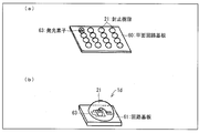
- Modification 2 In the present embodiment, the method of manufacturing the plurality of light emitting devices 1d by mounting the plurality of light emitting elements 63 on the planar circuit board 60 and simultaneously sealing the light emitting elements 63 has been described. You may manufacture the single light emitting device 1e using the manufacturing method of a device.
- FIG. 27A a pair of mounting wiring patterns 74 and a connecting wiring pattern 76 are provided on a circuit board 71 having a flat surface, and light is emitted on the mounting wiring pattern 74.
- the element 73 is bonded.
- the light emitting element 73 and the mounting wiring pattern 74 are wire-bonded by a conductive line 77b made of a gold wire or the like, and the light emitting element 73 and the connection wiring pattern 76 are made of a conductive wire 77a made of a gold wire or the like. Wire bonding is performed (mounting step).
- the mounting wiring pattern 74 and the connecting wiring pattern 76 are provided with a resin dam mechanism 78 for holding the molten silicone resin on the upper surface of the circuit board 71. Then, the circuit board 71 on which the light emitting element 73 is mounted is set on the heat plate 79, and the separated sealing resin sheet 20 is disposed at a position facing the upper surface of the light emitting element 73 (arrangement step).
- the circuit board 71 is heated from below by the hot plate 79 (melting step), and the sealing resin sheet 20 is melted.
- the sealing resin sheet 20 separated into pieces is arranged at a position facing the upper surface of the light emitting element 73 mounted on the circuit board 71 without using a mechanism for pressurization. Then, the light emitting device 1e can be manufactured by heating.
- a transparent resin layer having a dome shape, a lens shape, or the like that does not include a phosphor (the same silicone as the sealing resin sheet 20) is used to adjust the light distribution characteristics of the light emitting device 1e.
- a resin or another resin material may be formed as appropriate.
- the phosphor concentration between the light emitting devices can be made equal by using the sealing resin sheet 20 in which the phosphor is uniformly dispersed and separated into the same size.
- the manufacturing method of the light-emitting device according to the present embodiment is a mixed powder for sealing in which a silicone resin powder and a phosphor used in the sealing resin sheet 20 are mixed instead of the sealing resin sheet 20.
- (Encapsulant) 120 is mainly different from Embodiment 1 in that it is used.
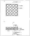
- FIGS. 28A to 28D are schematic views showing a method for manufacturing a light emitting device according to this embodiment.
- a sealing mixed powder 120 in which a silicone resin powder and a phosphor are mixed is applied to the entire surface of the multiple cavity circuit board 10 on which the light emitting element 13 is mounted.
- Sprinkling (or coating) as shown in FIG. 28B, the entire multi-cavity circuit board 10 is covered with the mixed powder 120 for sealing (placement step).
- This encapsulating mixed powder 120 is made of a silicone resin having the viscosity characteristics shown in FIG. 4, and the powder of the first cross-linked but semi-cured silicone resin and the phosphor are uniformly dispersed in the phosphor.
- the method of powdering the silicone resin is not particularly limited, and examples thereof include a method of pulverizing to a diameter of about 10 ⁇ m at a low temperature using a jet mill having a cooling function.
- the powder of the silicone resin that has undergone the secondary crosslinking reaction may be further mixed.
- the silicone resin that has undergone the secondary cross-linking reaction maintains a fully cured state even when heated in a curing step or the like. Therefore, by mixing the powder of the silicone resin that has undergone the secondary crosslinking reaction with the mixed powder 120 for sealing, the mixed powder 120 for sealing filled in the cavity 12 is heated, and the silicone that has undergone the primary crosslinking reaction Sedimentation of the phosphor that can occur when the resin is in a molten state can be suppressed.
- the squeegee 36 is moved along the surface of the multi-cavity circuit board 10 while abutting it, so that the seal adhered to the surface of the multi-cavity circuit board 10 is obtained.
- the stopping mixed powder 120 is removed.
- each of the cavities 12 of the multiple cavity circuit board 10 is filled with the sealing mixed powder 120.
- the content of the phosphor contained in the sealing mixed powder 120 filled (arranged) in each cavity 12 is substantially equalized.
- the mixed powder 120 for sealing removed from the surface of the multi-cavity circuit board 10 is an uncured resin that has undergone a primary crosslinking reaction but has not undergone a secondary crosslinking reaction. It is possible.
- the multiple cavity circuit board 10 is inserted into the vacuum heating furnace 33 and heated, as shown in FIG.
- the mixed powder 120 for sealing is heated to about 100 ° C. by the vacuum heating furnace 33, the silicone resin powder in each cavity 12 is melted, and the silicone resin melted by the vacuum heating furnace 33 being evacuated. Is degassed (melting step). Thereafter, when the silicone resin is further heated to a high temperature of about 150 ° C. by the vacuum heating furnace 33, the silicone resin is cured by secondary crosslinking (curing step).
- the multiple cavity circuit board 10 is divided for each cavity 12, whereby a light emitting device in which the light emitting element 13 in the cavity 12 is sealed with the sealing resin 21 can be obtained.
- the sealing resin 21 is compared with the method using the individual sealing resin sheet 20 shown in FIGS. 27 (a) to 27 (c).
- the uniformity of the dispersed state of the phosphor can be easily improved.
- a powdery silicone resin and a phosphor are mixed, and thus the phosphor can be sufficiently dispersed without being affected by the viscosity of the silicone resin. This is because the dispersion state of the phosphor in the mixed powder 120 for sealing can be made more uniform.
- FIG. 29 is a table showing various data relating to the method for manufacturing the light emitting device according to the present embodiment.
- FIG. 29 as a comparative example, the data by the conventional casting sealing method shown in FIG. 8 and the sheet resin method of Embodiment 1 are shown together.
- the conventional casting sealing method has 15 ranks, and the sheet resin method of Embodiment 1 has 3 ranks, whereas the powder of this embodiment has In the coating method, the chromaticity distribution width is one rank, and the dispersion of chromaticity values is greatly improved.
- the unnecessary mixture powder 120 for sealing adhering to the surface of the multiple cavity circuit board 10 between the cavities 12 can be removed without significantly affecting the body concentration and the amount of the phosphor. This is because the amount of the sealed mixed powder 120 to be filled can be controlled more reliably than other methods.
- the particle size of the silicone resin powder particles and the phosphor particles are different.
- the particle size of the silicone resin powder particles and the phosphor particles are different.
- the light emitting device manufactured by the powder coating method of the present embodiment has X and Y values as compared with the light emitting device manufactured by the conventional casting sealing method and the sheet resin method of the first embodiment. Since the value is small and the rank (division) value is small, it can be seen that the variation in chromaticity values among the light-emitting devices that are mass-produced is very small.
- the conventional casting sealing method has a rank of 50 parts, and the sheet resin method of Embodiment 1 has 10 parts, whereas the powder coating method of this embodiment has In principle, the amount of waste resin / phosphor is zero. This is because, in the powder coating method of this embodiment, in the step of filling each cavity 12 with the sealing mixed powder 120, the excess sealing mixed powder 120 overflowing from the cavity 12 is collected and re-applied. This is because it can be used.
- the amount of waste resin / phosphor becomes zero in principle, and it can be seen that it is extremely economical.
- the light emitting element 13 in the cavity 12 is sealed.
- the silicone resin powder and the phosphor are sufficiently mixed until the dispersed state of the phosphor becomes uniform.
- the content of the phosphor contained in the encapsulating mixed powder 120 can be almost equalized.
- FIG. 30 is a schematic view showing a manufacturing process of the sealing resin powder 121 which is a silicone resin powder including a phosphor.
- the sealing resin powder 121 is a powder in which a phosphor is uniformly dispersed in a silicone resin having viscosity characteristics shown in FIG. As shown in FIG. 30, this sealing resin powder 121 is a jet resin having a cooling function of a kneaded resin 24 (see FIG. 9C), which is a silicone resin 22 in which phosphors are uniformly dispersed. It can be obtained by crushing to a diameter of about 25 ⁇ m using a mill at a low temperature.
- the cavity 12 may be sealed using a sealing resin tablet (sealing material) 122 formed into a tablet shape by pressing and solidifying the sealing mixed powder 120 or the sealing resin powder 121.
- a sealing resin tablet sealing material
- FIG. 31 (a) to 31 (c) are schematic views showing a method for manufacturing a light emitting device using the sealing resin tablet 122.
- FIG. 31A a sealing resin tablet 122 is disposed in the cavity 12 formed in the circuit board 11 (arrangement step).
- This sealing resin tablet 122 is formed into a tablet by pressing and solidifying the sealing mixed powder 120 shown in FIG. 28A or the sealing resin powder 121 shown in FIG.
- the adhesiveness between the silicone resin powder and the phosphor and between the silicone resin powder including the phosphor can be improved, and can be easily integrated (tablet).
- the sealing resin tablet 122 is heated by heating the circuit board 11 from below with the hot plate 79 in a state where the sealing resin tablet 122 is disposed in the cavity 12. Is melted (melting step).
- the molten silicone resin at a state of being in close contact with the upper surface and the side surface of the light emitting element 13, a silicone resin by to secondary crosslinking heated further to secondary crosslinking temperature T 1 of Is fully cured (curing step).
- the sealing resin 21 can be formed and the light emitting device 1f can be manufactured.
- the light emitting device 1f can be manufactured by heating the sealing resin tablet 122 disposed in the cavity 12 without using a mechanism for making a vacuum. .
- the powder between the silicone resin and the phosphor, and the phosphor are included. Since voids do not occur between the silicone resin powders, the volumetric shrinkage of the silicone resin after heating can be reduced. Therefore, sealing suitable for the size of the cavity 12 is possible, and variation in chromaticity values between the light emitting devices 1f can be further reduced.
- the handleability of the sealing mixed powder 120 and the sealing resin powder 121 can be improved.
- the cavity 12 may be sealed using a sealing mixed powder sheet (sealing resin sheet / sealing material) 123 formed into a sheet by pressing and solidifying the sealing mixed powder 120 described above.
- a sealing mixed powder sheet sealing resin sheet / sealing material
- 32 (a) to 32 (e) are schematic views showing a method for producing a sealing mixed powder sheet 123 obtained by forming the sealing mixed powder 120 shown in FIG. 28 (a) into a sheet. .
- the first-crosslinked semi-cured silicone resin powder and the phosphor are sufficiently mixed until the dispersed state is uniform, and mixed powder for sealing. Get 120.
- the mixed powder 120 for sealing is put into a mold, and as shown in FIG. 32 (c), compression molding is performed using the pressure plate 30.
- the mixed powder 120 for sealing is molded into a sheet shape.
- the manufacturing process for manufacturing the sealing resin sheet 20 by forming the kneaded resin 24 as shown in FIGS. 9A to 9E into a sheet Low temperature because the temperature adjustment function for adjusting the viscosity of the silicone resin during kneading and the expensive kneading equipment with wear resistance to the phosphor are not required (dry blend method).
- the mixed powder sheet 123 for sealing can be manufactured in a short time and at a low cost.
- the mixed powder sheet 123 for sealing thus manufactured can be used in place of the sealing resin sheet 20 shown in FIG.
- the mixed powder 120 for sealing used for manufacturing the mixed powder sheet 123 for sealing is further mixed with a powder of a silicone resin that has been completely cured by secondary crosslinking.
- the secondary cross-linked silicone resin powder is mixed with the sealing mixed powder 120 to form a sheet.
- the mixed powder sheet for sealing 123 is separated into individual pieces, and the light emitting elements 13 are individually sealed using the mixed powder sheet for sealing 123 separated into pieces. Good.
- the method for manufacturing a light-emitting device includes a mounting step of mounting at least one light-emitting element on a substrate, and a position facing the top surface of the light-emitting element mounted in the mounting step.
- An arrangement step of arranging a sealing material including at least a silicone resin that has been semi-cured by secondary crosslinking and a phosphor, and the silicone resin that has been first crosslinked with the sealing material arranged in the arrangement step A melting step in which the sealing material is melted by heating at a temperature lower than the secondary crosslinking temperature, which is a temperature at which the resin is completely cured by secondary crosslinking, A curing step of heating the sealing material at a temperature equal to or higher than the secondary cross-linking temperature in a state where the sealing material melted in the melting step is in close contact with at least the upper surface of the light emitting element.
- the silicone resin is characterized in that the viscosity is reversibly lowered in a temperature range from room temperature to less than the secondary cross-linking temperature, and is irreversibly fully cured in a temperature range higher than the secondary cross-linking temperature.
- a sealing material including at least a silicone resin that has been semi-cured by primary crosslinking and a phosphor is disposed at a position facing the upper surface of the light-emitting element mounted on the substrate.
- the silicone resin has a viscosity that reversibly decreases in a temperature range from room temperature to less than the secondary cross-linking temperature, and is irreversibly fully cured in a temperature range higher than the secondary cross-linking temperature. Therefore, the viscosity of the silicone resin can be repeatedly controlled by changing the temperature in the temperature range from room temperature to less than the secondary crosslinking temperature.
- the phosphor when the phosphor is kneaded into this silicone resin, the phosphor is uniformly dispersed in the silicone resin by controlling (lowering) the viscosity of the silicone resin so that the kneaded phosphor does not settle. It becomes possible.
- a sealing material in which the phosphor is uniformly dispersed in the silicone resin can be obtained. Therefore, by sealing the light emitting element using this sealing material, It is possible to realize a method for manufacturing a light-emitting device that can equalize the phosphor concentrations and reduce variations in chromaticity values due to the phosphor concentration and phosphor content.
- the encapsulating material arranged in the arranging step is an encapsulating mixture in which the silicone resin powder subjected to primary crosslinking and the phosphor are mixed at least.
- a powder is preferred.
- the dispersion state of the phosphor with respect to the sealing mixed powder is made uniform by thoroughly mixing the powder of the first-crosslinked silicone resin and the phosphor.
- the mixed powder for sealing is further mixed with a powder of the silicone resin that has been fully cured by secondary crosslinking. .
- the mixed powder for sealing is further mixed with a powder of silicone resin that has been fully cured by secondary crosslinking.
- the melting step and the curing are included by including the secondary cross-linked silicone resin powder in the sealing mixed powder. Sedimentation of the phosphor in the step can be suppressed.
- the dispersion state of the phosphor in the light emitting device can be improved.
- the sealing material disposed in the placing step includes at least the first crosslinked silicone resin and includes a sheet including the phosphor.
- a resin sheet is preferred.
- the sealing resin sheet kneads the phosphor in the silicone resin that has been subjected to primary crosslinking and heated at a temperature lower than the secondary crosslinking temperature. It is preferable that the kneaded resin obtained in this way is made into a sheet.
- a kneaded resin in which the phosphor is uniformly dispersed in the silicone resin is obtained by kneading the phosphor with the silicone resin while controlling the viscosity of the silicone resin so that the phosphor does not settle. be able to.
- the concentration of the phosphors between the light emitting devices can be equalized by disposing the sealing resin sheet formed from the kneaded resin in the disposing step.
- the sealing resin sheet is formed by pressing and sealing a mixed powder for sealing in which at least the powder of the silicone resin subjected to primary crosslinking and the phosphor are mixed.
- a sheet is preferable.
- the encapsulating resin sheet is obtained by pressing and solidifying the encapsulating mixed powder in which at least the first-crosslinked silicone resin powder and the phosphor are mixed. Therefore, a temperature adjustment function for adjusting the viscosity of the silicone resin at the time of kneading, which is essential in the above-described method for producing a sealing resin sheet for producing a sealing resin sheet by kneading the kneaded resin, and The resin sheet for sealing can be easily manufactured without using expensive kneading equipment having wear resistance to the phosphor.
- the sealing resin sheet can be manufactured in a low cost and in a short time.
- the mixed powder for sealing is further mixed with the powder of the silicone resin that has been fully cured by secondary crosslinking.
- the mixed powder for sealing is further mixed with a powder of silicone resin that has been fully cured by secondary crosslinking.
- the secondary cross-linked silicone resin is cured by mixing the secondary cross-linked silicone resin powder into a mixed powder for sealing in order to maintain a fully cured state even during heating in a curing step or the like.
- a sealing resin sheet that can suppress sedimentation of the phosphor during heating such as in steps can be manufactured.
- the dispersion state of the phosphor in the light emitting device can be improved.
- the encapsulating material disposed in the arranging step includes an encapsulating resin powder made of the silicone resin powder that is primarily crosslinked and includes the phosphor. It is preferable that
- the sealing resin powder kneads the phosphor in the silicone resin that has been subjected to primary crosslinking and heated at a temperature lower than the secondary crosslinking temperature. It is preferable that the kneaded resin obtained in this way is powdered.
- a kneaded resin in which the phosphor is uniformly dispersed in the silicone resin is obtained by kneading the phosphor with the silicone resin while controlling the viscosity of the silicone resin so that the phosphor does not settle. be able to.
- the light emitting element in the mounting step, the light emitting element is mounted in each cavity of the substrate in which a plurality of cavities opening upward are formed, and in the arranging step, As the sealing material, the sealing resin sheet is placed on the substrate so as to cover all the cavities formed in the substrate, and in the melting step, the molten sealing material is It is preferable that pressurization is performed so that the cavities are filled, and in the curing step, the primary-crosslinked silicone resin contained in the sealing material filled in the cavities is completely cured.
- a sealing resin sheet as a sealing material is stacked on the substrate so as to cover all the cavities formed on the substrate, and the molten sealing material (silicone resin) is contained in each cavity. Since the heating is performed while pressurizing so as to be filled in, the melted sealing material can be filled in each cavity at the same time. Then, the light-emitting elements mounted in the respective cavities can be simultaneously sealed by fully curing the primary cross-linked silicone resin contained in the sealing material filled in the cavities.
- the melted sealing material can be simultaneously filled in each cavity without using a special dispenser or molding machine for filling the melted sealing material into each cavity. Therefore, the production efficiency of the light emitting device can be remarkably improved.
- the substrate is provided with a through hole in each cavity.
- a through hole is provided in the sealing resin sheet at a position facing each cavity.
- the through hole is provided at a position facing each cavity of the sealing resin sheet, it is possible to promote the discharge of air in each cavity.
- a surface molding release sheet having a satin-like unevenness formed on the surface is further stacked and arranged,
- the primary cross-linked silicone resin contained in the sealing material is placed in a state where the surface forming release sheet is in contact with the surface of the sealing material filled in each cavity. It is preferable to completely cure.
- a surface-molding release sheet having a satin-like unevenness formed on the surface is placed on the sealing resin sheet, and in the curing step, the sealing filled in each cavity is placed.
- the primary cross-linked silicone resin contained in the sealing material is fully cured in a state where the surface forming release sheet is in contact with the surface of the stopper.
- a satin-like unevenness is formed on the surface of the fully cured silicone resin, and the light extraction efficiency of the light emitting device can be improved by the unevenness.
- a lens-forming resin sheet made of a light-transmitting resin is further arranged on the sealing resin sheet, and the melting step.
- the lens molding resin sheet is applied to the sealing resin sheet via a lens molding die having a lens molding recess formed at a position facing each light emitting element mounted on the substrate. It is preferable to press.
- a lens molding resin sheet made of a resin having optical transparency is further stacked on the sealing resin sheet. Then, the lens molding resin sheet is pressed toward the sealing resin sheet through a lens molding die in which lens molding recesses are formed at positions facing each cavity. Therefore, the resin constituting the molten lens molding resin sheet can be filled in the lens molding recess.
- a plurality of light emitting devices to which lenses are added can be simultaneously manufactured by curing the resin constituting the lens molding resin sheet in a state where the lens molding recesses are filled. .
- the light emitting device manufacturing method in the mounting step, a plurality of the light emitting elements are mounted on the substrate having a flat surface, and in the arranging step, the light emitting device is mounted on the substrate as the sealing material.
- the sealing resin sheet formed with a plurality of recesses capable of accommodating each light emitting element is disposed on the substrate such that each light emitting element is accommodated in the recess, and in the melting step, A pressure is applied through a lens molding die in which a lens molding recess is formed at a position facing each light emitting element mounted on the substrate so that the melted sealing material is filled in each lens molding recess.
- a sealing resin sheet in which a plurality of light emitting elements are mounted on a substrate having a flat surface and a plurality of recesses capable of accommodating each light emitting element mounted on the substrate is formed.
- Each light emitting element is placed on the substrate so as to be accommodated in the recess.
- the sealing resin sheet is pressed toward the substrate through a lens molding die in which a lens molding recess is formed at a position facing each light emitting element mounted on the substrate. Therefore, the melted sealing material can be filled in each lens molding recess, and the primary crosslinked silicone resin contained in the sealing material in the lens molding recess can be fully cured by secondary crosslinking.
- a plurality of light emitting devices in which the sealing material is formed into a lens shape can be manufactured simultaneously.
- a mounting step in which a plurality of openings capable of accommodating the light emitting elements is formed and at least an inner surface of each opening has a reflecting function.
- the plurality of light emitting elements are mounted on the substrate having a flat surface, and in the placing step, each light emitting element mounted on the substrate is accommodated in the opening.
- the reflection plate is placed on the substrate, and the sealing resin sheet is used as the sealing material in the placement step, and all the openings formed in the reflection plate placed on the substrate.
- the silicone resin which is a primary crosslinking included in Hama has been the sealing material is preferred.
- the sealing resin sheet as the sealing material is disposed on the reflector so as to cover all the openings formed in the reflector. Then, the sealing resin sheet is heated while being pressurized so that the melted silicone resin is filled in each opening, and the primary cross-linked lycon resin contained in the sealing material filled in each opening is completely removed. Harden. Therefore, the melted sealing material can be simultaneously filled in each opening, and the light emitting element mounted in each opening can be simultaneously sealed.
- the sealing resin sheet is pressed by a vacuum pressure toward the substrate in the melting step.
- the sealing resin sheet is heated while being pressurized toward the substrate by vacuum, the air in each cavity can be surely discharged, and the air is contained in the molten silicone resin. It can suppress mixing.
- the sealing resin sheet is heated and pressurized by a vacuum hot press apparatus.
- the sealing resin sheets having different phosphor contents are arranged in a stack in the arranging step.
- the dispersion concentration of the phosphor can be easily controlled by changing the combination of the sealing resin sheets. Can do.
- the sealing resin sheet is heated and pressurized by a vacuum impregnation apparatus.
- the heating process under high pressure can be easily performed in the vacuum impregnation apparatus, so that the working efficiency can be improved.
- the light emitting element in the mounting step, the light emitting element is mounted in the cavity of the substrate in which a cavity opening upward is formed, and in the arranging step, the sealing is performed. It is preferable that the sealing mixed powder is disposed in the cavity in which the light emitting element is mounted as a stopper.
- the concentration of the phosphors between the light emitting devices is easily equalized by arranging the mixed powder for sealing as a sealing material in the cavity in which the light emitting element is mounted. be able to.
- the mixed powder for sealing is pressed into a tablet shape.
- the light emitting element in the mounting step, the light emitting element is mounted in the cavity of the substrate in which a cavity opening upward is formed, and in the arranging step, the sealing is performed.
- the sealing resin powder is preferably disposed in the cavity in which the light emitting element is mounted.
- the concentration of the phosphor between the light emitting devices is easily equalized by disposing the sealing resin powder as the sealing material in the cavity in which the light emitting element is mounted. be able to.
- the sealing resin powder is pressed into a tablet.
- voids are less likely to be generated between the silicone resins including the phosphor, so that the volumetric shrinkage of the silicone resin generated after heating can be reduced.
- the silicone resin is melted in a vacuum environment in the melting step.
- the silicone resin melted in the cavity 12 can be degassed by melting the silicone resin in a vacuum environment.
- the adhesion between the inner surface of the cavity and the fully cured silicone resin can be improved.
- the present invention can be suitably used, for example, for manufacturing a light emitting device used for a display device using LED as a light source, a lighting fixture, a backlight such as a display, a traffic light, a large outdoor display, an advertisement signboard, and the like.
Abstract
Description
本発明に係る発光デバイスの製造方法に関する実施の一形態について、図1~図20に基づいて説明すれば以下のとおりである。
An embodiment relating to a method for manufacturing a light emitting device according to the present invention will be described below with reference to FIGS.
まず、本実施形態に係る発光デバイス1aの構成について、図1を参照して説明する。 <Configuration of light emitting device>
First, the configuration of the light emitting device 1a according to the present embodiment will be described with reference to FIG.
次に、図1に示される発光デバイス1aの製造方法について、図2~図8を参照して説明する。 <Method for manufacturing light-emitting device>
Next, a method for manufacturing the light-emitting device 1a shown in FIG. 1 will be described with reference to FIGS.
次に、本実施形態に係る発光デバイスの製造方法に用いられる封止用樹脂シート20の製造方法について、図9~図11を参照して説明する。 <The manufacturing method of the
Next, a method for manufacturing the sealing
以上のように、本実施形態に係る発光デバイスの製造方法は、多連キャビティ回路基板10に形成された各キャビティ12内に発光素子13をそれぞれ実装する実装ステップと、発光素子13が実装された全てのキャビティ12を覆うように、1次架橋により半硬化状態となったシリコーン樹脂と、蛍光体とを含む封止用樹脂シート20を多連キャビティ回路基板10に重ねて配置する配置ステップと、封止用樹脂シート20を、当該シリコーン樹脂が2次架橋により全硬化する温度である2次架橋温度T1未満の温度で加熱しつつ、溶融したシリコーン樹脂が各キャビティ12内に充填されるように加圧する溶融ステップと、各キャビティ12内に充填された溶融したシリコーン樹脂22を各発光素子13の少なくとも上面に密着させた状態で、2次架橋温度T1以上で加熱する硬化ステップとを含み、シリコーン樹脂は、室温T0から2次架橋温度T1未満までの温度領域で可逆的に粘度が低下し、2次架橋温度T1以上の温度領域で非可逆的に全硬化する。 <Summary of
As described above, in the method for manufacturing a light emitting device according to this embodiment, the mounting step of mounting the
次に、本実施形態に係る発光デバイスの製造方法の変形例について、図12~図20を参照して説明する。 <Modification>
Next, a modification of the method for manufacturing the light emitting device according to the present embodiment will be described with reference to FIGS.
本実施形態では、発光素子13が実装された多連キャビティ回路基板10と、封止用樹脂シート20と、表面成形用離型シート31と、重り板32とを重ねた状態で、真空加熱炉33によって真空状態で加熱する方法について説明したが、重り板32を使用しない方法であってもよい。 (Modification 1)
In the present embodiment, the vacuum heating furnace in a state where the multiple
また、本実施形態では、多連キャビティ回路基板10上に封止用樹脂シート20を重ねて配置して加熱する方法について説明したが、この場合、各キャビティ12の底部に、一対の貫通孔12aをそれぞれ設けておいてもよい。 (Modification 2)
In the present embodiment, the sealing
本実施形態では、1つの封止用樹脂シート20を用いて発光素子13を封止する方法について説明したが、蛍光体の含有率がそれぞれ異なる複数の封止用樹脂シートを重ねて発光素子13を封止してもよい。 (Modification 3)
In the present embodiment, the method of sealing the
本実施形態では、封止用樹脂シート20上に表面成形用離型シート31を配置する方法について説明したが、表面成形用離型シート31に代えて、レンズ成形用樹脂シート25を配置してもよい。 (Modification 4)
In the present embodiment, the method of disposing the surface
本発明に係る発光デバイスの製造方法に関する他の実施の一形態について、図21~図27に基づいて説明すれば以下のとおりである。なお、説明の便宜上、上述した実施形態にて説明した図面と同じ機能を有する部材については、同じ符号を付記し、その説明を省略する。 [Embodiment 2]
Another embodiment of the method for manufacturing a light emitting device according to the present invention will be described below with reference to FIGS. For convenience of explanation, members having the same functions as those of the drawings described in the above-described embodiments are denoted by the same reference numerals and description thereof is omitted.
まず、実施形態に係る発光デバイスの製造方法について、図21~図23を参照して説明する。 <Method for manufacturing light-emitting device>
First, a method for manufacturing a light emitting device according to an embodiment will be described with reference to FIGS.
以上のように、本実施形態に係る発光デバイスの製造方法は、表面が平坦な平面回路基板60に複数の発光素子13を実装する実装ステップと、実装された各発光素子63を収容可能な複数の凹部26aが形成された封止用樹脂シート26を、各発光素子63が当該凹部26a内にそれぞれ収容されるように平面回路基板60上に配置する配置ステップと、配置した封止用樹脂シート26を、平面回路基板60に実装された各発光素子63に対向する位置にレンズ成形用凹部35fが形成されたレンズ成形用金型35dを介して加圧しながら加熱する加熱スッテップと、溶融させたシリコーン樹脂を、各レンズ成形用凹部35f内で、2次架橋により全硬化させる硬化ステップとを含んでいる。 <Summary of
As described above, the method for manufacturing a light emitting device according to this embodiment includes a mounting step of mounting a plurality of
次に、本実施形態に係る発光デバイスの製造方法の変形例について、図24~図27を参照して説明する。 <Modification>
Next, a modification of the method for manufacturing the light emitting device according to this embodiment will be described with reference to FIGS.
本実施形態では、凸レンズ型の封止樹脂21によって封止された発光デバイス1dの製造する方法について説明したが、本発明に係る発光デバイスの製造方法を用いてドットマトリクス型の発光表示デバイス50を製造することもできる。 (Modification 1)
In the present embodiment, the method for manufacturing the
本実施形態では、平面回路基板60上に複数の発光素子63を実装し、各発光素子63を同時に封止することで複数の発光デバイス1dを製造する方法について説明したが、本発明に係る発光デバイスの製造方法を用いて、単一の発光デバイス1eを製造してもよい。 (Modification 2)
In the present embodiment, the method of manufacturing the plurality of light emitting
本発明に係る発光デバイスの製造方法に関する別の実施の一形態について、図28~図31に基づいて説明すれば以下のとおりである。なお、説明の便宜上、上述した実施形態にて説明した図面と同じ機能を有する部材については、同じ符号を付記し、その説明を省略する。 [Embodiment 3]
Another embodiment of the light emitting device manufacturing method according to the present invention will be described below with reference to FIGS. For convenience of explanation, members having the same functions as those of the drawings described in the above-described embodiments are denoted by the same reference numerals and description thereof is omitted.
図28の(a)~図28の(d)は、本実施形態に係る発光デバイスの製造方法を示す概略図である。図28の(a)に示すように、まず、発光素子13が実装された多連キャビティ回路基板10の表面全体に、シリコーン樹脂の粉末と蛍光体とが混合された封止用混合粉末120を振りかけて(または、塗布して)、図28の(b)に示すように、多連キャビティ回路基板10全体が封止用混合粉末120にて覆われた状態とする(配置ステップ)。 <Method for manufacturing light-emitting device>
FIGS. 28A to 28D are schematic views showing a method for manufacturing a light emitting device according to this embodiment. As shown in FIG. 28A, first, a sealing
以上のように、本実施形態に係る発光デバイスの製造方法は、配置ステップにおいて、発光素子13が実装されたキャビティ12内に、シリコーン樹脂の粉末と蛍光体とが混合された封止用混合粉末120を充填した状態で加熱することで、キャビティ12内の発光素子13を封止するものである。 <Summary of Embodiment 3>
As described above, in the light emitting device manufacturing method according to the present embodiment, the sealing mixed powder in which the silicone resin powder and the phosphor are mixed in the
次に、本実施形態に係る発光デバイスの製造方法の変形例について、図30および図31を参照して説明する。 <Modification>
Next, a modification of the method for manufacturing a light emitting device according to this embodiment will be described with reference to FIGS.
本実施形態では、シリコーン樹脂の粉末と蛍光体とが混合された封止用混合粉末120を使用する方法について説明したが、封止用混合粉末120に代えて、蛍光体を包含するシリコーン樹脂の粉末からなる封止用樹脂粉末121(封止材)を使用してもよい。 (Modification 1)
In this embodiment, the method of using the sealing
上述の封止用混合粉末120または封止用樹脂粉末121を押し固めることでタブレット状に成形した封止用樹脂タブレット(封止材)122を用いてキャビティ12を封止してもよい。 (Modification 2)
The
上述の封止用混合粉末120を押し固めることでシート状に成形した封止用混合粉末シート(封止用樹脂シート・封止材)123を用いてキャビティ12を封止してもよい。 (Modification 3)
The
以上のように、本発明に係る発光デバイスの製造方法は、基板に、少なくとも1つの発光素子を実装する実装ステップと、前記実装ステップにて実装した前記発光素子の上面と対向する位置に、1次架橋により半硬化状態となったシリコーン樹脂と、蛍光体とを少なくとも含む封止材を配置する配置ステップと、前記配置ステップにて配置した前記封止材を、1次架橋された前記シリコーン樹脂が2次架橋により全硬化する温度である2次架橋温度未満の温度で加熱して、前記封止材を溶融させる溶融ステップと、
前記溶融ステップにて溶融した前記封止材を前記発光素子の少なくとも上面に密着させた状態で、前記封止材を前記2次架橋温度以上の温度で加熱する硬化ステップとを含み、
前記シリコーン樹脂は、室温から前記2次架橋温度未満までの温度領域で可逆的に粘度が低下し、前記2次架橋温度以上の温度領域で非可逆的に全硬化することを特徴とする。 [Summary of Embodiment]
As described above, the method for manufacturing a light-emitting device according to the present invention includes a mounting step of mounting at least one light-emitting element on a substrate, and a position facing the top surface of the light-emitting element mounted in the mounting step. An arrangement step of arranging a sealing material including at least a silicone resin that has been semi-cured by secondary crosslinking and a phosphor, and the silicone resin that has been first crosslinked with the sealing material arranged in the arrangement step A melting step in which the sealing material is melted by heating at a temperature lower than the secondary crosslinking temperature, which is a temperature at which the resin is completely cured by secondary crosslinking,
A curing step of heating the sealing material at a temperature equal to or higher than the secondary cross-linking temperature in a state where the sealing material melted in the melting step is in close contact with at least the upper surface of the light emitting element.
The silicone resin is characterized in that the viscosity is reversibly lowered in a temperature range from room temperature to less than the secondary cross-linking temperature, and is irreversibly fully cured in a temperature range higher than the secondary cross-linking temperature.
1b 発光デバイス
1c 発光デバイス
1d 発光デバイス
1e 発光デバイス
1f 発光デバイス
10 多連キャビティ回路基板(基板)
11 回路基板(基板)
12 キャビティ
12a 貫通孔
13 発光素子
14,54,64,74 マウント用配線パターン
15,65 導電性接着剤
16,56,66,76 接続用配線パターン
17,57,67,77a,77b 導電線
20 封止用樹脂シート(封止材)
20a 貫通孔
20A 第1の封止用樹脂シート(封止用樹脂シート・封止材)
20B 第2の封止用樹脂シート(封止用樹脂シート・封止材)
21 封止樹脂
24 混錬樹脂
25 レンズ成形用樹脂シート
26 封止用樹脂シート(封止材)
26a 凹部
31 表面成形用離型シート
32 重り板
33 真空加熱炉
35 真空熱プレス装置
35a ヒーター台
35b プレスヒーター
35e レンズ成形用溝部(レンズ成形用凹部)
35h 固定具凹部
38a 真空引き用袋
38c 加熱炉
38d 真空ポンプ
40 真空加熱装置
41 上部チャンバー
42 下部チャンバー
43 ダイヤフラムゴム
44,79 熱板
50 発光表示デバイス(発光デバイス)
51 平面回路基板(基板)
53 発光素子
58 反射板
58a 開口部
60 平面回路基板(基板)
61 回路基板(基板)
63,73 発光素子
120 封止用混合粉末(封止材)
121 封止用樹脂粉末(封止材)
122 封止用樹脂タブレット(封止用混合粉末・封止用樹脂粉末・封止材)
123 封止用混合粉末シート(封止用樹脂シート・封止材)
132a 開口部
T0 室温
T1 2次架橋温度 DESCRIPTION OF SYMBOLS 1a
11 Circuit board (board)
12
20a Through-
20B Second sealing resin sheet (sealing resin sheet / sealant)
21 sealing resin 24 kneaded
26a
35h Fixing
51 Planar circuit board (board)
53 Light Emitting Element 58
61 Circuit board (board)
63,73
121 Resin powder for sealing (sealing material)
122 Resin tablet for sealing (mixed powder for sealing, resin powder for sealing, sealing material)
123 Mixed powder sheet for sealing (resin sheet for sealing / sealing material)
132a Opening T 0 Room temperature T 1 Secondary cross-linking temperature
Claims (25)
- 基板に、少なくとも1つの発光素子を実装する実装ステップと、
前記実装ステップにて実装した前記発光素子の上面と対向する位置に、1次架橋により半硬化状態となったシリコーン樹脂と、蛍光体とを少なくとも含む封止材を配置する配置ステップと、
前記配置ステップにて配置した前記封止材を、1次架橋された前記シリコーン樹脂が2次架橋により全硬化する温度である2次架橋温度未満の温度で加熱して、前記封止材を溶融させる溶融ステップと、
前記溶融ステップにて溶融した前記封止材を前記発光素子の少なくとも上面に密着させた状態で、前記封止材を前記2次架橋温度以上の温度で加熱する硬化ステップとを含み、
前記シリコーン樹脂は、室温から前記2次架橋温度未満までの温度領域で可逆的に粘度が低下し、前記2次架橋温度以上の温度領域で非可逆的に全硬化することを特徴とする発光デバイスの製造方法。 A mounting step of mounting at least one light emitting element on the substrate;
An arrangement step of disposing a sealing material including at least a silicone resin that has been semi-cured by primary crosslinking and a phosphor at a position facing the upper surface of the light emitting element mounted in the mounting step;
The sealing material disposed in the placing step is heated at a temperature lower than a secondary crosslinking temperature, which is a temperature at which the silicone resin subjected to primary crosslinking is fully cured by secondary crosslinking, thereby melting the sealing material. A melting step,
A curing step of heating the sealing material at a temperature equal to or higher than the secondary cross-linking temperature in a state where the sealing material melted in the melting step is in close contact with at least the upper surface of the light emitting element.
The silicone resin has a viscosity reversibly lowered in a temperature range from room temperature to less than the secondary cross-linking temperature, and is irreversibly fully cured in a temperature range higher than the secondary cross-linking temperature. Manufacturing method. - 前記配置ステップにおいて配置される前記封止材は、1次架橋された前記シリコーン樹脂の粉末と前記蛍光体とが少なくとも混合された封止用混合粉末であることを特徴とする請求項1に記載の発光デバイスの製造方法。 The said sealing material arrange | positioned in the said arrangement | positioning step is the mixed powder for sealing by which the powder of the said silicone resin and the said fluorescent substance which were primarily bridge | crosslinked at least were mixed. Method of manufacturing a light emitting device.
- 前記封止用混合粉末には、2次架橋により全硬化状態となった前記シリコーン樹脂の粉末がさらに混合されていることを特徴とする請求項2に記載の発光デバイスの製造方法。 3. The method for manufacturing a light-emitting device according to claim 2, wherein the mixed powder for sealing is further mixed with powder of the silicone resin that has been completely cured by secondary crosslinking.
- 前記配置ステップにおいて配置される前記封止材は、1次架橋された前記シリコーン樹脂を少なくとも含む、前記蛍光体を包含したシートからなる封止用樹脂シートであることを特徴とする請求項1に記載の発光デバイスの製造方法。 The said sealing material arrange | positioned in the said arrangement | positioning step is a resin sheet for sealing which consists of a sheet | seat including the said fluorescent substance containing at least the silicone resin by which the primary bridge | crosslinking was carried out. The manufacturing method of the light-emitting device of description.
- 前記封止用樹脂シートは、前記2次架橋温度未満の温度で加熱した、1次架橋された前記シリコーン樹脂に、前記蛍光体を混錬することで得られた混錬樹脂をシート化したものであることを特徴とする請求項4に記載の発光デバイスの製造方法。 The sealing resin sheet is a sheet obtained by forming a kneaded resin obtained by kneading the phosphor into the silicone resin that has been primarily crosslinked and heated at a temperature lower than the secondary crosslinking temperature. The method for manufacturing a light-emitting device according to claim 4, wherein:
- 前記封止用樹脂シートは、1次架橋された前記シリコーン樹脂の粉末と前記蛍光体とが少なくとも混合された封止用混合粉末を押し固めてシート化したものであることを特徴とする請求項4に記載の発光デバイスの製造方法。 The sealing resin sheet is a sheet obtained by pressing and solidifying a mixed powder for sealing in which at least the powder of the silicone resin subjected to primary crosslinking and the phosphor are mixed. 5. A method for producing a light-emitting device according to 4.
- 前記封止用混合粉末には、2次架橋により全硬化状態となった前記シリコーン樹脂の粉末がさらに混合されていることを特徴とする請求項6に記載の発光デバイスの製造方法。 The method for manufacturing a light emitting device according to claim 6, wherein the mixed powder for sealing is further mixed with the powder of the silicone resin that has been completely cured by secondary crosslinking.
- 前記配置ステップにおいて配置される前記封止材は、前記蛍光体を包含する、1次架橋された前記シリコーン樹脂の粉末からなる封止用樹脂粉末であることを特徴とする請求項1に記載の発光デバイスの製造方法。 The said sealing material arrange | positioned in the said arrangement | positioning step is the resin powder for sealing which consists of the powder of the said silicone resin by which 1st bridge | crosslinking including the said fluorescent substance was carried out. Manufacturing method of light emitting device.
- 前記封止用樹脂粉末は、前記2次架橋温度未満の温度で加熱した、1次架橋された前記シリコーン樹脂に、前記蛍光体を混錬することで得られた混錬樹脂を粉末化したものであることを特徴とする請求項8に記載の発光デバイスの製造方法。 The encapsulating resin powder is obtained by pulverizing a kneaded resin obtained by kneading the phosphor with the primary crosslinked silicone resin heated at a temperature lower than the secondary crosslinking temperature. The method for manufacturing a light emitting device according to claim 8, wherein:
- 前記実装ステップにおいて、上方に向かって開口する複数のキャビティが形成された前記基板の各キャビティ内に前記発光素子をそれぞれ実装し、
前記配置ステップにおいて、前記封止材として、前記封止用樹脂シートを、前記基板に形成された全てのキャビティを覆うように前記基板上に重ねて配置し、
前記溶融ステップにおいて、溶融した前記封止材が各キャビティ内に充填されるように加圧し、
前記硬化ステップにおいて、各キャビティ内に充填された前記封止材に含まれる1次架橋された前記シリコーン樹脂を全硬化させることを特徴とする請求項4から7のいずれか1項に記載の発光デバイスの製造方法。 In the mounting step, each of the light emitting elements is mounted in each cavity of the substrate in which a plurality of cavities opening upward are formed,
In the placing step, as the sealing material, the sealing resin sheet is placed on the substrate so as to cover all the cavities formed in the substrate,
In the melting step, pressurization is performed so that the melted sealing material is filled in each cavity,
8. The light emitting device according to claim 4, wherein, in the curing step, the first-crosslinked silicone resin contained in the sealing material filled in each cavity is completely cured. 9. Device manufacturing method. - 前記基板には、各キャビティに貫通孔が設けられていることを特徴とする請求項10に記載の発光デバイスの製造方法。 The method for manufacturing a light emitting device according to claim 10, wherein the substrate is provided with a through hole in each cavity.
- 前記封止用樹脂シートには、各キャビティと対向する位置に貫通孔が設けられていることを特徴とする請求項10または11に記載の発光デバイスの製造方法。 The method for manufacturing a light emitting device according to claim 10 or 11, wherein the sealing resin sheet is provided with a through hole at a position facing each cavity.
- 前記配置ステップにおいて、前記封止用樹脂シート上に、表面に梨地状の凹凸が形成された表面成形用離型シートをさらに重ねて配置し、
前記硬化ステップにおいて、各キャビティ内に充填された前記封止材の表面に前記表面成形用離型シートを当接させた状態で、前記封止材に含まれる1次架橋された前記シリコーン樹脂を全硬化させることを特徴とする請求項10から12のいずれか1項に記載の発光デバイスの製造方法。 In the arranging step, on the sealing resin sheet, a surface molding release sheet having a satin-like unevenness formed on the surface is further stacked and arranged,
In the curing step, the primary cross-linked silicone resin contained in the sealing material is placed in a state where the surface forming release sheet is in contact with the surface of the sealing material filled in each cavity. The method for producing a light-emitting device according to claim 10, wherein the light-emitting device is fully cured. - 前記配置ステップにおいて、前記封止用樹脂シート上に、光透過性を有する樹脂からなるレンズ成形用樹脂シートをさらに重ねて配置し、
前記溶融ステップにおいて、前記基板に実装された各発光素子に対向する位置にレンズ成形用凹部が形成されたレンズ成形用金型を介して、前記レンズ成形用樹脂シートを前記封止用樹脂シートに向けて加圧することを特徴とする請求項10から12のいずれか1項に記載の発光デバイスの製造方法。 In the arrangement step, a lens molding resin sheet made of a resin having light permeability is further stacked on the sealing resin sheet,
In the melting step, the lens molding resin sheet is formed into the sealing resin sheet through a lens molding die in which a lens molding recess is formed at a position facing each light emitting element mounted on the substrate. The method for manufacturing a light-emitting device according to claim 10, wherein the pressure is applied toward the surface. - 前記実装ステップにおいて、表面が平坦な前記基板に複数の前記発光素子を実装し、
前記配置ステップにおいて、前記封止材として、前記基板に実装された各発光素子を収容可能な複数の凹部が形成された前記封止用樹脂シートを、各発光素子が前記凹部内にそれぞれ収容されるように前記基板上に配置し、
前記溶融ステップにおいて、前記基板に実装された各発光素子に対向する位置にレンズ成形用凹部が形成されたレンズ成形用金型を介して、溶融した前記封止材が各レンズ成形用凹部に充填されるように加圧し、
前記硬化ステップにおいて、各レンズ成形用凹部内に充填された前記封止材に含まれる1次架橋された前記シリコーン樹脂を全硬化させることを特徴とする請求項4から7のいずれか1項に記載の発光デバイスの製造方法。 In the mounting step, a plurality of the light emitting elements are mounted on the substrate having a flat surface,
In the arrangement step, the sealing resin sheet formed with a plurality of recesses capable of accommodating the light emitting elements mounted on the substrate is used as the sealing material, and the light emitting elements are accommodated in the recesses, respectively. Placed on the substrate so that
In the melting step, the melted sealing material is filled in each lens molding recess through a lens molding die in which a lens molding recess is formed at a position facing each light emitting element mounted on the substrate. Pressurize as
8. The method according to claim 4, wherein, in the curing step, the first-crosslinked silicone resin contained in the sealing material filled in each lens molding recess is completely cured. The manufacturing method of the light-emitting device of description. - 前記発光素子を収容可能な複数の開口部が形成され、且つ、少なくとも各開口部の内面が反射機能を有する反射板を載置する載置ステップをさらに含み、
前記実装ステップにおいて、表面が平坦な前記基板に複数の前記発光素子を実装し、
前記載置ステップにおいて、前記基板に実装された各発光素子が前記開口部内にそれぞれ収容されるように、前記反射板を前記基板上に載置し、
前記配置ステップにおいて、前記封止材として、前記封止用樹脂シートを、前記基板に載置された前記反射板に形成された全ての開口部を覆うように前記反射板上に配置し、
前記溶融ステップにおいて、溶融した前記封止材が各開口部に充填されるように加圧し、
前記硬化ステップにおいて、各開口部内に充填された前記封止材に含まれる1次架橋された前記シリコーン樹脂を全硬化させることを特徴とする請求項4から7のいずれか1項に記載の発光デバイスの製造方法。 A plurality of openings that can accommodate the light emitting elements, and at least an inner surface of each of the openings further includes a mounting step of mounting a reflecting plate;
In the mounting step, a plurality of the light emitting elements are mounted on the substrate having a flat surface,
In the placing step, the reflective plate is placed on the substrate so that each light emitting element mounted on the substrate is accommodated in the opening, respectively.
In the arranging step, as the sealing material, the sealing resin sheet is arranged on the reflecting plate so as to cover all openings formed in the reflecting plate placed on the substrate,
In the melting step, pressurization is performed so that the melted sealing material is filled in each opening,
8. The light emitting device according to claim 4, wherein, in the curing step, the first-crosslinked silicone resin contained in the sealing material filled in each opening is fully cured. 9. Device manufacturing method. - 前記溶融ステップにおいて、前記封止用樹脂シートを、前記基板に向けて真空圧により加圧することを特徴とする請求項10から16のいずれか1項に記載の発光デバイスの製造方法。 The method for manufacturing a light emitting device according to any one of claims 10 to 16, wherein, in the melting step, the sealing resin sheet is pressurized by a vacuum pressure toward the substrate.
- 前記封止用樹脂シートを、真空熱プレス装置によって加熱および加圧することを特徴とする請求項17に記載の発光デバイスの製造方法。 The method for manufacturing a light emitting device according to claim 17, wherein the sealing resin sheet is heated and pressurized by a vacuum hot press apparatus.
- 前記配置ステップにおいて、蛍光体の含有率がそれぞれ異なる前記封止用樹脂シートを重ねて配置することを特徴とする請求項10から18のいずれか1項に記載の発光デバイスの製造方法。 The method for manufacturing a light-emitting device according to any one of claims 10 to 18, wherein, in the arranging step, the sealing resin sheets having different phosphor contents are arranged to overlap each other.
- 前記封止用樹脂シートを、真空含浸装置によって加熱および加圧することを特徴とする請求項17に記載の発光デバイスの製造方法。 The method for manufacturing a light-emitting device according to claim 17, wherein the sealing resin sheet is heated and pressurized by a vacuum impregnation apparatus.
- 前記実装ステップにおいて、上方に向かって開口するキャビティが形成された前記基板の前記キャビティ内に前記発光素子を実装し、
前記配置ステップにおいて、前記封止材として、前記封止用混合粉末を、前記発光素子が実装された前記キャビティ内に配置することを特徴とする請求項2または3に記載の発光デバイスの製造方法。 In the mounting step, the light emitting element is mounted in the cavity of the substrate in which a cavity opening upward is formed,
4. The method of manufacturing a light emitting device according to claim 2, wherein in the arranging step, the mixed powder for sealing is arranged as the sealing material in the cavity in which the light emitting element is mounted. 5. . - 前記封止用混合粉末は、タブレット状に押し固められていることを特徴とする請求項21に記載の発光デバイスの製造方法。 The method for manufacturing a light emitting device according to claim 21, wherein the mixed powder for sealing is pressed into a tablet shape.
- 前記実装ステップにおいて、上方に向かって開口するキャビティが形成された前記基板の前記キャビティ内に前記発光素子を実装し、
前記配置ステップにおいて、前記封止材として、前記封止用樹脂粉末を、前記発光素子が実装された前記キャビティ内に配置することを特徴とする請求項8または9に記載の発光デバイスの製造方法。 In the mounting step, the light emitting element is mounted in the cavity of the substrate in which a cavity opening upward is formed,
The light emitting device manufacturing method according to claim 8 or 9, wherein, in the arranging step, the sealing resin powder is arranged as the sealing material in the cavity in which the light emitting element is mounted. . - 前記封止用樹脂粉末は、タブレット状に押し固められていることを特徴とする請求項23に記載の発光デバイスの製造方法。 The method for manufacturing a light emitting device according to claim 23, wherein the sealing resin powder is pressed into a tablet.
- 前記溶融ステップにおいて、真空環境下で前記シリコーン樹脂を溶融させることを特徴とする請求項21から24のいずれか1項に記載の発光デバイスの製造方法。 The method for manufacturing a light emitting device according to any one of claims 21 to 24, wherein, in the melting step, the silicone resin is melted in a vacuum environment.
Priority Applications (8)
| Application Number | Priority Date | Filing Date | Title |
|---|---|---|---|
| EP12854299.0A EP2787543B1 (en) | 2011-11-29 | 2012-06-25 | Manufacturing method for light-emitting device |
| US14/348,742 US9006006B2 (en) | 2011-11-29 | 2012-06-25 | Manufacturing method for light-emitting device comprising multi-step cured silicon resin |
| KR1020147008816A KR101404911B1 (en) | 2011-11-29 | 2012-06-25 | Manufacturing method for light-emitting device |
| CN201280045615.5A CN103814448B (en) | 2011-11-29 | 2012-06-25 | Manufacturing method for light-emitting device |
| KR1020147009111A KR20140088088A (en) | 2011-11-29 | 2012-06-25 | Sealing member, and method for producing fluorescent material-containing sealing member |
| EP15001377.9A EP2924744B1 (en) | 2011-11-29 | 2012-06-25 | Manufacturing method for light-emitting device |
| JP2013506388A JP5407007B2 (en) | 2011-11-29 | 2012-06-25 | Method for manufacturing light emitting device |
| US14/670,256 US20150200341A1 (en) | 2011-11-29 | 2015-03-26 | Manufacturing method for light-emitting device |
Applications Claiming Priority (4)
| Application Number | Priority Date | Filing Date | Title |
|---|---|---|---|
| JP2011260936 | 2011-11-29 | ||
| JP2011-260936 | 2011-11-29 | ||
| JP2012019150 | 2012-01-31 | ||
| JP2012-019150 | 2012-01-31 |
Related Child Applications (2)
| Application Number | Title | Priority Date | Filing Date |
|---|---|---|---|
| US14/348,742 A-371-Of-International US9006006B2 (en) | 2011-11-29 | 2012-06-25 | Manufacturing method for light-emitting device comprising multi-step cured silicon resin |
| US14/670,256 Continuation US20150200341A1 (en) | 2011-11-29 | 2015-03-26 | Manufacturing method for light-emitting device |
Publications (1)
| Publication Number | Publication Date |
|---|---|
| WO2013080596A1 true WO2013080596A1 (en) | 2013-06-06 |
Family
ID=48535075
Family Applications (1)
| Application Number | Title | Priority Date | Filing Date |
|---|---|---|---|
| PCT/JP2012/066174 WO2013080596A1 (en) | 2011-11-29 | 2012-06-25 | Manufacturing method for light-emitting device |
Country Status (7)
| Country | Link |
|---|---|
| US (2) | US9006006B2 (en) |
| EP (2) | EP2787543B1 (en) |
| JP (3) | JP5407007B2 (en) |
| KR (2) | KR20140088088A (en) |
| CN (2) | CN104993036A (en) |
| TW (2) | TWI563694B (en) |
| WO (1) | WO2013080596A1 (en) |
Cited By (5)
| Publication number | Priority date | Publication date | Assignee | Title |
|---|---|---|---|---|
| JP2016522978A (en) * | 2013-03-15 | 2016-08-04 | ダウ コーニング コーポレーションDow Corning Corporation | Method of manufacturing an optical assembly comprising depositing a solid silicone-containing hot melt composition in powder form and forming an encapsulant thereof |
| WO2016136243A1 (en) * | 2015-02-25 | 2016-09-01 | 東レ・ダウコーニング株式会社 | Curable granular silicone composition and method for preparing same |
| JP2017506003A (en) * | 2014-01-21 | 2017-02-23 | コーニンクレッカ フィリップス エヌ ヴェKoninklijke Philips N.V. | Hybrid chip on board LED module with patterned encapsulant |
| JP2017520918A (en) * | 2014-06-04 | 2017-07-27 | ダウ コーニング コーポレーションDow Corning Corporation | Imprint process of hot-melt curable silicone composition for optical devices |
| JP2019033264A (en) * | 2014-09-26 | 2019-02-28 | 東芝ホクト電子株式会社 | Light emitting module and manufacturing method thereof |
Families Citing this family (17)
| Publication number | Priority date | Publication date | Assignee | Title |
|---|---|---|---|---|
| KR102304432B1 (en) * | 2012-09-19 | 2021-09-17 | 어플라이드 머티어리얼스, 인코포레이티드 | Methods for bonding substrates |
| CN105659397B (en) * | 2013-10-15 | 2018-04-20 | 夏普株式会社 | Light-emitting device |
| CN110047987B (en) * | 2014-05-21 | 2023-10-20 | 亮锐控股有限公司 | Method for attaching lens to LED module with high alignment accuracy |
| US10622522B2 (en) * | 2014-09-05 | 2020-04-14 | Theodore Lowes | LED packages with chips having insulated surfaces |
| US10411176B2 (en) * | 2014-09-12 | 2019-09-10 | Semicon Light Co., Ltd. | Method for manufacturing semiconductor light-emitting device |
| US9887110B2 (en) * | 2014-09-27 | 2018-02-06 | Intel Corporation | Substrate warpage control using temper glass with uni-directional heating |
| US9627591B2 (en) * | 2015-02-25 | 2017-04-18 | Nichia Corporation | Mounting substrate and electronic device including the same |
| KR102396332B1 (en) | 2015-09-22 | 2022-05-12 | 삼성전자주식회사 | Fine interval coating member for led dispaly and coating method using the same |
| WO2017136383A1 (en) * | 2016-02-02 | 2017-08-10 | Maintool SAS | Flexible electronic strip and its method for manufacture |
| JP6394649B2 (en) * | 2016-06-30 | 2018-09-26 | 日亜化学工業株式会社 | Method for manufacturing light emitting device |
| WO2018183341A1 (en) | 2017-03-27 | 2018-10-04 | Firouzeh Sabri | Light weight flexible temperature sensor kit |
| US10147787B1 (en) | 2017-05-31 | 2018-12-04 | Taiwan Semiconductor Manufacturing Co., Ltd. | Semiconductor structure and manufacturing method thereof |
| JP2019086129A (en) * | 2017-11-09 | 2019-06-06 | 三菱重工業株式会社 | Sealing method, assembly and method for manufacturing assembly |
| JP7095937B2 (en) * | 2018-03-09 | 2022-07-05 | ミネベアミツミ株式会社 | Manufacturing method of fluorescent sheet |
| CN113272976A (en) * | 2018-12-27 | 2021-08-17 | 电化株式会社 | Phosphor substrate, light-emitting substrate, and lighting device |
| JP7022285B2 (en) * | 2019-07-02 | 2022-02-18 | 日亜化学工業株式会社 | Light emitting device and its manufacturing method |
| TWI720785B (en) * | 2020-01-15 | 2021-03-01 | 東貝光電科技股份有限公司 | Micro led light emitting device and manufacturing method thereof |
Citations (10)
| Publication number | Priority date | Publication date | Assignee | Title |
|---|---|---|---|---|
| JP2006140362A (en) | 2004-11-15 | 2006-06-01 | Nitto Denko Corp | Optical semiconductor device sealing sheet and optical semiconductor device manufacturing method using the same |
| JP2006229054A (en) | 2005-02-18 | 2006-08-31 | Nichia Chem Ind Ltd | Light-emitting device |
| JP2008211205A (en) | 2007-02-12 | 2008-09-11 | Cree Inc | Method of forming packaged semiconductor light-emitting device having multiple optical elements by compression molding |
| JP2009010109A (en) | 2007-06-27 | 2009-01-15 | Namics Corp | Method of manufacturing seal body of light emitting diode chip |
| JP2009259868A (en) * | 2008-04-11 | 2009-11-05 | Sharp Corp | Chromaticity adjusting method of light-emitting apparatus and manufacturing method |
| JP2010027974A (en) * | 2008-07-23 | 2010-02-04 | Sharp Corp | Method of manufacturing light-emitting device |
| JP2010159411A (en) | 2008-12-12 | 2010-07-22 | Nitto Denko Corp | Semi-cured silicone resin sheet |
| JP2010285593A (en) * | 2008-12-12 | 2010-12-24 | Nitto Denko Corp | Composition for thermosetting silicone resin |
| JP2011138831A (en) * | 2009-12-25 | 2011-07-14 | Toyoda Gosei Co Ltd | Manufacturing method for light-emitting device |
| WO2011102272A1 (en) * | 2010-02-19 | 2011-08-25 | 東レ株式会社 | Phosphor-containing cured silicone, process for production of same, phosphor-containing silicone composition, precursor of the composition, sheet-shaped moldings, led package, light -emitting device, and process for production of led-mounted substrate |
Family Cites Families (31)
| Publication number | Priority date | Publication date | Assignee | Title |
|---|---|---|---|---|
| DE4001431A1 (en) * | 1990-01-19 | 1991-07-25 | Hoechst Ag | Hot melt adhesives with extended pot life - contg. acrylic! copolymer, metal chelate crosslinker, extender etc., and crosslinking regulator, pref. A-stage alkyl-phenolic resin |
| JP2994219B2 (en) | 1994-05-24 | 1999-12-27 | シャープ株式会社 | Method for manufacturing semiconductor device |
| JP4271747B2 (en) | 1997-07-07 | 2009-06-03 | 株式会社朝日ラバー | Translucent coating material for light emitting diode and fluorescent color light source |
| US6623670B2 (en) | 1997-07-07 | 2003-09-23 | Asahi Rubber Inc. | Method of molding a transparent coating member for light-emitting diodes |
| US6319425B1 (en) | 1997-07-07 | 2001-11-20 | Asahi Rubber Inc. | Transparent coating member for light-emitting diodes and a fluorescent color light source |
| TW459403B (en) * | 2000-07-28 | 2001-10-11 | Lee Jeong Hoon | White light-emitting diode |
| JP3909826B2 (en) | 2001-02-23 | 2007-04-25 | 株式会社カネカ | Light emitting diode |
| US6924596B2 (en) * | 2001-11-01 | 2005-08-02 | Nichia Corporation | Light emitting apparatus provided with fluorescent substance and semiconductor light emitting device, and method of manufacturing the same |
| JP2003262701A (en) * | 2002-03-08 | 2003-09-19 | Kanegafuchi Chem Ind Co Ltd | Composition for optical material, optical material, liquid crystal display device and light emitting diode obtained by using the same, and method for manufacturing them |
| KR100558446B1 (en) * | 2003-11-19 | 2006-03-10 | 삼성전기주식회사 | Manfucturing method of molding compound resin tablet and manfucturing method of a white light emitting diode using the same |
| US7087465B2 (en) * | 2003-12-15 | 2006-08-08 | Philips Lumileds Lighting Company, Llc | Method of packaging a semiconductor light emitting device |
| JP2005217369A (en) * | 2004-02-02 | 2005-08-11 | Three M Innovative Properties Co | Adhesive sheet for light-emitting-diode device, and light-emitting-diode device |
| TWI398188B (en) * | 2004-08-31 | 2013-06-01 | Showa Denko Kk | A luminous body, and a lighting and display device using the luminous body |
| KR101204115B1 (en) | 2005-02-18 | 2012-11-22 | 니치아 카가쿠 고교 가부시키가이샤 | Light emitting device with light distribution characteristic controlling lens |
| JP2007091960A (en) | 2005-09-30 | 2007-04-12 | Nitto Denko Corp | Resin composition for sealing optical semiconductor element and optical semiconductor device obtained by using the same |
| DE102005047500B4 (en) * | 2005-10-04 | 2013-12-05 | Ems-Chemie Ag | Plastic component with visible part and light source |
| JP2007235104A (en) * | 2006-01-31 | 2007-09-13 | Toshiba Lighting & Technology Corp | Light emitting device and manufacturing method thereof |
| JP5428122B2 (en) * | 2006-05-11 | 2014-02-26 | 日亜化学工業株式会社 | Resin molded product and molding method thereof, and light emitting device and manufacturing method thereof |
| JP2008300544A (en) * | 2007-05-30 | 2008-12-11 | Sharp Corp | Light-emitting device, and manufacturing method thereof |
| WO2009038020A1 (en) * | 2007-09-19 | 2009-03-26 | Toray Industries, Inc. | Adhesive composition for electronic components and adhesive sheet for electronic components using the same |
| EP2328994B1 (en) * | 2008-09-16 | 2012-12-26 | Koninklijke Philips Electronics N.V. | Polymeric wavelength converting elements |
| EP2196503B1 (en) | 2008-12-12 | 2015-02-18 | Nitto Denko Corporation | Thermosetting silicone resin composition, silicone resin, silicone resin sheet and use thereof |
| CN101834235B (en) * | 2009-03-10 | 2013-01-16 | 亿光电子工业股份有限公司 | Light-emitting diode packaging structure and manufacture method thereof |
| JP4913858B2 (en) * | 2009-04-14 | 2012-04-11 | 日東電工株式会社 | Composition for thermosetting silicone resin |
| JP2011082339A (en) * | 2009-10-07 | 2011-04-21 | Nitto Denko Corp | Kit for optical semiconductor encapsulation |
| JP5744386B2 (en) * | 2009-10-07 | 2015-07-08 | 日東電工株式会社 | Optical semiconductor encapsulant |
| JP5894723B2 (en) | 2009-12-29 | 2016-03-30 | 株式会社朝日ラバー | Manufacturing method of semiconductor light emitting device |
| JP5328705B2 (en) | 2010-03-26 | 2013-10-30 | 日東電工株式会社 | Composition for silicone resin |
| JP5775375B2 (en) * | 2010-07-27 | 2015-09-09 | 日東電工株式会社 | Method for manufacturing light emitting diode device |
| JP5767062B2 (en) * | 2010-09-30 | 2015-08-19 | 日東電工株式会社 | Light emitting diode sealing material and method for manufacturing light emitting diode device |
| JP2012102167A (en) | 2010-11-05 | 2012-05-31 | Nitto Denko Corp | Silicone resin, sealing material, and optical semiconductor device |
-
2012
- 2012-06-25 CN CN201510270212.6A patent/CN104993036A/en active Pending
- 2012-06-25 EP EP12854299.0A patent/EP2787543B1/en not_active Not-in-force
- 2012-06-25 US US14/348,742 patent/US9006006B2/en not_active Expired - Fee Related
- 2012-06-25 KR KR1020147009111A patent/KR20140088088A/en not_active Application Discontinuation
- 2012-06-25 WO PCT/JP2012/066174 patent/WO2013080596A1/en active Application Filing
- 2012-06-25 KR KR1020147008816A patent/KR101404911B1/en active IP Right Grant
- 2012-06-25 EP EP15001377.9A patent/EP2924744B1/en not_active Not-in-force
- 2012-06-25 CN CN201280045615.5A patent/CN103814448B/en not_active Expired - Fee Related
- 2012-06-25 JP JP2013506388A patent/JP5407007B2/en not_active Expired - Fee Related
- 2012-07-06 TW TW103108048A patent/TWI563694B/en not_active IP Right Cessation
- 2012-07-06 TW TW101124507A patent/TWI435480B/en not_active IP Right Cessation
-
2013
- 2013-03-21 JP JP2013059156A patent/JP5705254B2/en not_active Expired - Fee Related
-
2015
- 2015-02-24 JP JP2015034589A patent/JP5917739B2/en not_active Expired - Fee Related
- 2015-03-26 US US14/670,256 patent/US20150200341A1/en not_active Abandoned
Patent Citations (10)
| Publication number | Priority date | Publication date | Assignee | Title |
|---|---|---|---|---|
| JP2006140362A (en) | 2004-11-15 | 2006-06-01 | Nitto Denko Corp | Optical semiconductor device sealing sheet and optical semiconductor device manufacturing method using the same |
| JP2006229054A (en) | 2005-02-18 | 2006-08-31 | Nichia Chem Ind Ltd | Light-emitting device |
| JP2008211205A (en) | 2007-02-12 | 2008-09-11 | Cree Inc | Method of forming packaged semiconductor light-emitting device having multiple optical elements by compression molding |
| JP2009010109A (en) | 2007-06-27 | 2009-01-15 | Namics Corp | Method of manufacturing seal body of light emitting diode chip |
| JP2009259868A (en) * | 2008-04-11 | 2009-11-05 | Sharp Corp | Chromaticity adjusting method of light-emitting apparatus and manufacturing method |
| JP2010027974A (en) * | 2008-07-23 | 2010-02-04 | Sharp Corp | Method of manufacturing light-emitting device |
| JP2010159411A (en) | 2008-12-12 | 2010-07-22 | Nitto Denko Corp | Semi-cured silicone resin sheet |
| JP2010285593A (en) * | 2008-12-12 | 2010-12-24 | Nitto Denko Corp | Composition for thermosetting silicone resin |
| JP2011138831A (en) * | 2009-12-25 | 2011-07-14 | Toyoda Gosei Co Ltd | Manufacturing method for light-emitting device |
| WO2011102272A1 (en) * | 2010-02-19 | 2011-08-25 | 東レ株式会社 | Phosphor-containing cured silicone, process for production of same, phosphor-containing silicone composition, precursor of the composition, sheet-shaped moldings, led package, light -emitting device, and process for production of led-mounted substrate |
Non-Patent Citations (2)
| Title |
|---|
| "TX-2506 Series", DOW CORNING CORPORATION |
| See also references of EP2787543A4 |
Cited By (5)
| Publication number | Priority date | Publication date | Assignee | Title |
|---|---|---|---|---|
| JP2016522978A (en) * | 2013-03-15 | 2016-08-04 | ダウ コーニング コーポレーションDow Corning Corporation | Method of manufacturing an optical assembly comprising depositing a solid silicone-containing hot melt composition in powder form and forming an encapsulant thereof |
| JP2017506003A (en) * | 2014-01-21 | 2017-02-23 | コーニンクレッカ フィリップス エヌ ヴェKoninklijke Philips N.V. | Hybrid chip on board LED module with patterned encapsulant |
| JP2017520918A (en) * | 2014-06-04 | 2017-07-27 | ダウ コーニング コーポレーションDow Corning Corporation | Imprint process of hot-melt curable silicone composition for optical devices |
| JP2019033264A (en) * | 2014-09-26 | 2019-02-28 | 東芝ホクト電子株式会社 | Light emitting module and manufacturing method thereof |
| WO2016136243A1 (en) * | 2015-02-25 | 2016-09-01 | 東レ・ダウコーニング株式会社 | Curable granular silicone composition and method for preparing same |
Also Published As
| Publication number | Publication date |
|---|---|
| EP2787543A1 (en) | 2014-10-08 |
| EP2787543B1 (en) | 2017-03-22 |
| JPWO2013080596A1 (en) | 2015-04-27 |
| TWI563694B (en) | 2016-12-21 |
| EP2924744A1 (en) | 2015-09-30 |
| CN103814448A (en) | 2014-05-21 |
| CN103814448B (en) | 2015-07-01 |
| US20150200341A1 (en) | 2015-07-16 |
| KR20140088088A (en) | 2014-07-09 |
| TW201322500A (en) | 2013-06-01 |
| US20150004726A1 (en) | 2015-01-01 |
| EP2787543A4 (en) | 2014-12-17 |
| KR101404911B1 (en) | 2014-06-09 |
| JP2015146426A (en) | 2015-08-13 |
| CN104993036A (en) | 2015-10-21 |
| TWI435480B (en) | 2014-04-21 |
| JP2013179300A (en) | 2013-09-09 |
| TW201424053A (en) | 2014-06-16 |
| KR20140049611A (en) | 2014-04-25 |
| JP5407007B2 (en) | 2014-02-05 |
| US9006006B2 (en) | 2015-04-14 |
| JP5917739B2 (en) | 2016-05-18 |
| JP5705254B2 (en) | 2015-04-22 |
| EP2924744B1 (en) | 2019-03-06 |
Similar Documents
| Publication | Publication Date | Title |
|---|---|---|
| JP5917739B2 (en) | Method for producing phosphor-containing encapsulant | |
| JP2994219B2 (en) | Method for manufacturing semiconductor device | |
| KR100665121B1 (en) | Method of producing wavelength-converted light emitting diode package | |
| KR101416758B1 (en) | Method for producing resin sealed electronic component and resin sealing device for electronic component | |
| TWI519571B (en) | Process for producing phosphor-containing sealant, phosphor-containing sealant, method for manufacturing light-emitting device, and dispenser | |
| JP6560498B2 (en) | Resin sealing method and resin molded product manufacturing method | |
| EP2219242A2 (en) | Sheet for photosemiconductor encapsulation | |
| US20140141283A1 (en) | Method for manufacturing a fluorescent resin film and fluorescent resin film manufactured thereby | |
| DE102007017855A1 (en) | Method for producing an optoelectronic component and optoelectronic component | |
| JP2006302965A (en) | Semiconductor light-emitting device and manufacturing method thereof | |
| WO2017221606A1 (en) | Optical semiconductor element having phosphor layer, and method for manufacturing optical semiconductor element | |
| KR101867304B1 (en) | Method of fabricating light emitting apparatus | |
| JP5816483B2 (en) | Manufacturing method of semiconductor light emitting device | |
| CN110459481A (en) | The packaging method of semiconductor element and its to position mould | |
| KR20130027709A (en) | Method for manufacturing led reflector | |
| KR101658446B1 (en) | Method of manufacturing luminescence powder resin film and luminescence powder resin film manufactured thereby | |
| JP7189465B2 (en) | Method for manufacturing package and method for manufacturing light-emitting device | |
| TWI402922B (en) | Molding method of semiconductor chips | |
| CN111128983A (en) | Method for manufacturing package and method for manufacturing light emitting device |
Legal Events
| Date | Code | Title | Description |
|---|---|---|---|
| ENP | Entry into the national phase |
Ref document number: 2013506388 Country of ref document: JP Kind code of ref document: A |
|
| 121 | Ep: the epo has been informed by wipo that ep was designated in this application |
Ref document number: 12854299 Country of ref document: EP Kind code of ref document: A1 |
|
| REEP | Request for entry into the european phase |
Ref document number: 2012854299 Country of ref document: EP |
|
| WWE | Wipo information: entry into national phase |
Ref document number: 2012854299 Country of ref document: EP |
|
| WWE | Wipo information: entry into national phase |
Ref document number: 14348742 Country of ref document: US |
|
| ENP | Entry into the national phase |
Ref document number: 20147008816 Country of ref document: KR Kind code of ref document: A |
|
| NENP | Non-entry into the national phase |
Ref country code: DE |