WO2013073435A1 - 屈折率センサ - Google Patents
屈折率センサ Download PDFInfo
- Publication number
- WO2013073435A1 WO2013073435A1 PCT/JP2012/078872 JP2012078872W WO2013073435A1 WO 2013073435 A1 WO2013073435 A1 WO 2013073435A1 JP 2012078872 W JP2012078872 W JP 2012078872W WO 2013073435 A1 WO2013073435 A1 WO 2013073435A1
- Authority
- WO
- WIPO (PCT)
- Prior art keywords
- refractive index
- layer
- optical
- index layer
- multilayer film
- Prior art date
- Legal status (The legal status is an assumption and is not a legal conclusion. Google has not performed a legal analysis and makes no representation as to the accuracy of the status listed.)
- Ceased
Links
Images













Classifications
-
- G—PHYSICS
- G01—MEASURING; TESTING
- G01N—INVESTIGATING OR ANALYSING MATERIALS BY DETERMINING THEIR CHEMICAL OR PHYSICAL PROPERTIES
- G01N21/00—Investigating or analysing materials by the use of optical means, i.e. using sub-millimetre waves, infrared, visible or ultraviolet light
- G01N21/17—Systems in which incident light is modified in accordance with the properties of the material investigated
- G01N21/41—Refractivity; Phase-affecting properties, e.g. optical path length
- G01N21/4133—Refractometers, e.g. differential
Definitions
- the present invention relates to a refractive index sensor for measuring the refractive index of an object to be measured.
- Refractive index sensors are used in various industrial fields such as biochemistry, chemistry, and environmental analysis.
- a refractive index sensor using an optical fiber is cheaper than other sensors, and can be miniaturized, remotely controlled, possibility of multiplexing, convenience of design, electromagnetic It has the advantage of being less susceptible to the influence of the world, and many studies have been made in recent years.
- optical fiber refractive index sensors include, for example, fiber Bragg grating (FBG), long-period fiber grating (LPG), interferometers (Mach-Zehnder, Michelson, Fabry-Perot, etc.), taper, etc. It is classified into a technique using processing (for example, see Patent Document 1).
- an optical fiber refractive index sensor using a grating such as FBG or LPG has high sensitivity but cannot obtain high spatial resolution.
- an optical fiber refractive index sensor using an interferometer and a taper process has high sensitivity and high spatial resolution, but the sensing head is likely to be physically damaged.
- an optical fiber refractive index sensor using an interferometer and a taper process can be applied only to the measurement of the refractive index of a liquid or gas, and the measurement system is complicated and expensive.
- the present invention has been proposed in view of such a situation, the sensing head is not easily damaged physically, can be applied to the measurement of the refractive index of liquid, gas and solid, and the measurement system is simple and inexpensive.
- An object is to provide a refractive index sensor.
- the present inventors have found that the center wavelength of the spectrum of the reflected light reflected by the object to be measured is incident on the optical band-pass filter is linearly shifted by the refractive index of the object to be measured. It came to do.
- the refractive index sensor includes a light source unit that outputs light, a dielectric multilayer film formed on one end surface of the optical transmission line, and one end in contact with the optical transmission line on the other end side.
- An optical bandpass filter in which an object to be measured having a predetermined refractive index is in contact with a dielectric multilayer film, and light output from a light source unit is incident through an optical transmission path, and an optical bandpass filter
- the refractive index calculation that calculates the refractive index of the reflected light based on the center wavelength of the spectrum of the reflected light measured by the measurement unit and the measurement unit that measures the spectrum of the reflected light reflected by the object to be measured
- the dielectric multilayer film includes a cavity layer disposed substantially at the center, a plurality of high refractive index layers on both sides of the cavity layer, and a plurality of low refractive index layers having a refractive index smaller than that of the high refractive index layer.
- Reflective multilayer film with high refractive index layer and low refraction Optical total thickness of the layers is lambda 0/2 when the center wavelength of the light output from the light source unit has a lambda 0, the optical thickness of each layer of the high refractive index layer and a low refractive index layer it is is a value different from each ⁇ 0/4.
- the refractive index measurement method includes an output step of outputting light, and a dielectric multilayer film is formed on one end surface of the optical transmission line, and one end contacting the optical transmission line is a dielectric on the other end side.
- the refractive index of the reflected light is calculated based on the measurement step of measuring the spectrum of the reflected light reflected by the object to be measured and the center wavelength of the spectrum of the reflected light measured in the measuring step.
- the dielectric multilayer film includes a cavity layer disposed substantially at the center, and a plurality of high refractive index layers and a plurality of refractive indexes smaller than the high refractive index layers on both sides of the cavity layer.
- a dielectric multilayer film is formed on one end surface of the optical transmission line, and one end in contact with the optical transmission line is on the dielectric multilayer film on the other end side.
- An optical bandpass filter in contact with an object to be measured having a predetermined refractive index, a light source unit that outputs light having a wavelength in the vicinity of the center wavelength of the optical bandpass filter and makes it incident through the optical transmission line, and the optical band Indicated by the detection unit that converts the optical power of the reflected light that is reflected by the object to be measured and returned by the measured object into an electric signal and detects the electric signal obtained as a detection output by the detection unit
- a refractive index calculation unit that calculates a refractive index of the reflected light based on the optical power of the reflected light, and the dielectric multilayer film is formed on a cavity layer disposed substantially in the center and on both sides of the cavity layer.
- a reflective multilayer film in which a plurality of low refractive index layers having a refractive index smaller than that of the high refractive index layer are stacked, and the optical thickness of the high refractive index layer and the low refractive index layer combined is , the center wavelength of light output from the light source unit is lambda 0/2 is taken as lambda 0, the optical thickness of each layer of the high refractive index layer and the low refractive index layer are each lambda 0 / This is a value different from 4.
- a dielectric multilayer film is formed on one end face of an optical transmission line, and the one end in contact with the optical transmission line is on a dielectric multilayer film on the other end side.
- a refractive index calculating step for calculating a refractive index of the reflected light, and the dielectric multilayer film includes a cavity layer disposed substantially at the center, a plurality of high refractive index layers and the high refractive index layers on both sides of the cavity layer.
- a reflective multilayer film in which a plurality of low refractive index layers having a refractive index smaller than that of the layer is laminated, and an optical thickness of the high refractive index layer and the low refractive index layer combined is output from the light source unit.
- a lambda 0/2 is taken as lambda 0 the center wavelength of the light
- the optical thickness of each layer of the high refractive index layer and the low refractive index layer is a different value than the lambda 0/4, respectively is there.
- the thickness of the high refractive index layer or the low refractive index layer in contact with the object to be measured is different depending on the thickness of the other high refractive index layer and the low refractive index layer. Can do.
- the cavity layer and the low refractive index layer are made of SiO 2 and have a thickness of 225 nm
- the high refractive index layer is made of TiO 2 and have a thickness of 225 nm
- the thickness of the high refractive index layer or the low refractive index layer in contact with the object to be measured is 1.7 times or more than the thickness of the other high refractive index layer and the low refractive index layer. can do.
- the total of the cavity layer, the high refractive index layer, and the low refractive index layer in the dielectric multilayer film may be 25 layers or more.
- the present invention it is possible to provide a refractive index sensor in which the sensing head is not easily damaged physically, can be applied to the measurement of the refractive index of liquid, gas and solid, and the measurement system is simple and inexpensive.
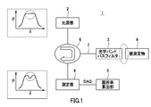
- FIG. 1 is a block diagram showing a configuration example of a refractive index sensor to which the present invention is applied.
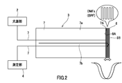
- FIG. 2 is a diagram schematically illustrating a configuration example of an optical bandpass filter.
- FIG. 3 is a cross-sectional view illustrating a configuration example of an optical bandpass filter.
- FIG. 4 is an electron micrograph of the optical bandpass filter.
- FIG. 5 is a diagram for explaining the measurement principle by the refractive index sensor to which the present invention is applied.
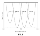
- FIG. 6 is a graph showing a simulation result of the refractive index dependence of the spectrum of reflected light.
- FIG. 7 is a graph showing a simulation result of the refractive index dependence of the center wavelength of the spectrum of reflected light.
- FIG. 1 is a block diagram showing a configuration example of a refractive index sensor to which the present invention is applied.
- FIG. 2 is a diagram schematically illustrating a configuration example of an optical bandpass filter.
- FIG. 3 is a cross-sectional
- FIG. 8 is a graph of experimental results showing the refractive index dependence of the spectrum of reflected light when a liquid is used for the object to be measured.
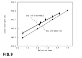
- FIG. 9 is a graph showing experimental results and simulation results of the refractive index dependence of the center wavelength of the spectrum of reflected light.
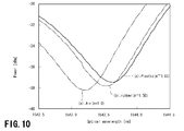
- FIG. 10 is a graph showing an experimental result of the refractive index dependence of the spectrum of reflected light when a solid is used as the object to be measured.
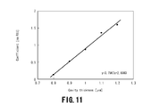
- FIG. 11 is a graph showing experimental results of the dependency of the thickness of the cavity layer on the sensitivity.
- FIG. 12 is a graph showing the dependency of the cavity layer thickness on the center wavelength of the reflected light spectrum.
- FIG. 13 is a graph showing experimental results of the thickness dependence of the high refractive index layer and the low refractive index layer with respect to sensitivity.
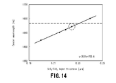
- FIG. 14 is a graph showing experimental results of the thickness dependence of the high refractive index layer and the low refractive index layer with respect to the center wavelength of the reflected light spectrum.
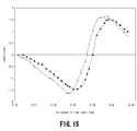
- FIG. 15 is a graph showing a simulation result of the thickness dependence of the uppermost layer of the dielectric multilayer film with respect to sensitivity.
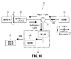
- FIG. 16 is a block diagram showing another configuration example of the refractive index sensor to which the present invention is applied.
- FIG. 19 is a diagram illustrating wavelengths at which the shift of the center wavelength in the optical bandpass filter can be detected as a linear change in optical power.
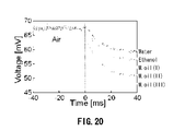
- FIG. 20 shows a state in which a liquid (water, ethanol, three kinds of refractive index matching oils) having various refractive indexes (n) is brought into contact as an object to be measured from a state where the optical bandpass filter is in contact with air.
- FIG. 21 is a graph showing the results of plotting the voltage when the refractive index is changed and stabilized against the refractive index.
- FIG. 22 shows the sensitivity of an optical fiber type refractive index sensor using an optical bandpass filter as a single mode optical fiber (standardized with the vertical axis assuming 100% of the light reflectance when air is in contact with the fiber end. It is the graph which shows the result of comparing the refractive index dependence of the light reflectivity with both compared with the sensitivity of a simple refractive index sensor using the intensity change of Fresnel reflection at the SMF (Single Mode Fiber) end.
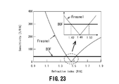
- FIG. 23 is a graph showing the result of comparing the sensitivity by differentiating the refractive index and taking the absolute value.
- FIG. 24 is a block diagram showing a configuration example of an ultrasonic detection apparatus to which the optical fiber type refractive index sensor is applied.
- FIG. 25 is a graph showing an ultrasonic detection result by the ultrasonic detection apparatus.
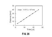
- FIG. 26 is a graph showing the result of plotting the distance against the time delay for the ultrasonic detection result by the ultrasonic detection apparatus.
- FIG. 27 is a graph showing the result of plotting the signal intensity Vp-p against the distance for the ultrasonic detection result by the ultrasonic detection apparatus.
- thickness refers to a physical thickness, that is, an actual thickness of a layer (film) of interest.
- optical thickness refers to a value obtained by multiplying the physical thickness by the refractive index of the film at the wavelength of the light, assuming that light of a certain wavelength passes through the film. .
- the present invention is applied to a refractive index sensor 1 configured as shown in the block diagram of FIG. 1, for example.
- the refractive index sensor 1 includes a light source unit 2, an optical bandpass filter 3, a measurement unit 4, and a refractive index calculation unit 5.
- the refractive index sensor 1 according to the embodiment of the first invention shown in FIG. 1 has a spectrum of reflected light obtained by reflecting the light incident on the optical bandpass filter 3 by the object to be measured 9 as will be described in detail later.
- the measurement principle is that the center wavelength of the signal shifts linearly with the refractive index of the object 9 to be measured.
- the light source unit 2 is composed of, for example, a broadband light source that emits broadband light, and outputs light as shown in FIG.
- the light source unit 2 can be composed of, for example, an ASE (Amplified Spontaneous Emission) light source that emits amplified spontaneous emission light.
- FIG. 2 is a diagram schematically showing a configuration example of the optical bandpass filter 3.
- the optical bandpass filter 3 for example, as shown in FIGS. 1 and 2, a dielectric multilayer film 8 is formed on one end surface 7A of an optical fiber 7 by vapor deposition.
- the optical bandpass filter 3 has a measured object made of a liquid, gas or solid having a predetermined refractive index on the dielectric multilayer film 8 on the side of the other end 8B from the one end 8A in contact with the optical fiber 7. 9 touches.
- the optical fiber 7 has a two-layer structure of a fiber core 7a and a clad 7b that covers the periphery of the fiber core 7a.
- the optical bandpass filter 3 can measure the refractive index of the DUT 9 in contact with the dielectric multilayer film 8 because the center wavelength of the structure shifts substantially linearly with respect to the refractive index. This is due to a change in Fresnel reflection that occurs at the contact surface between the dielectric multilayer film 8 and the DUT 9.
- FIG. 3 is a cross-sectional view showing a configuration example of the optical bandpass filter 3.
- FIG. 4 is a view showing an electron micrograph of the optical bandpass filter 3.
- the dielectric multilayer film 8 includes a cavity layer 10 disposed substantially at the center, and a plurality of high refractive index layers 11 and high refractive indexes on both sides in the thickness direction of the cavity layer 10.
- a reflective multilayer film in which a plurality of low refractive index layers 12 having a refractive index smaller than that of the layer 11 are alternately laminated.
- the dielectric multilayer film 8 functions as a band-pass filter that transmits only light of a specific wavelength.
- Optical total thickness of the high refractive index layer 11 and the low refractive index layer 12 is lambda 0/2 when the center wavelength of the light output from the light source unit 2 and the lambda 0. Further, the optical thickness of each layer of the high refractive index layer 11 and the low refractive index layer 12 is a value different from each ⁇ 0/4.
- the optical fiber end which has an optical band-pass filter 3 is present (one end surface 7A) It is possible to prevent the amount of reflected light reflected by the measurement object 9 reaching up to significantly decreasing. Thereby, it can prevent that a refractive index sensitivity falls.
- the reflective multilayer film is, for example, silicon, amorphous silicon, hydrogenated amorphous silicon, silicon dioxide, tantalum pentoxide, alumina, titanium dioxide, zirconium dioxide, hafnium dioxide, lanthanum dioxide, cerium dioxide, antimony trioxide, indium trioxide, oxidation Oxide such as magnesium and sodium dioxide, silicon oxynitride, silicon nitride, aluminum nitride, zirconium nitride, hafnium nitride, lanthanum nitride, etc., or magnesium fluoride, cerium trifluoride, It is composed of fluorides such as calcium fluoride, lithium monofluoride, and trisodium aluminum hexafluoride.
- the high refractive index layer or the low refractive index layer in contact with the object to be measured 9 that is, the thickness of the uppermost layer 13 is such that the high refractive index layer 11 other than the uppermost layer 13 and the low refractive index. It is preferable that the thickness varies depending on the thickness of the layer 12.
- the refractive index sensitivity can be made positive or negative, and zero. It has a positive maximum and a negative maximum. Therefore, the refractive index sensitivity of the refractive index sensor 1 can be controlled by changing the thickness of the uppermost layer 13.
- the cavity layer 10 and the low refractive index layer 12 are made of SiO 2 with a thickness of 225 nm
- the high refractive index layer 11 is made of TiO 2 with a thickness of 225 nm
- the high The thickness of the refractive index layer 11 or the low refractive index layer 12 is preferably 1.7 times or more than the thicknesses of the other high refractive index layers 11 and low refractive index layers 12.
- the dielectric multilayer film 8 includes the cavity layer 10, the high refractive index layer 11, and the low refractive index layer 12 from the viewpoint of improving the refractive index sensitivity of the refractive index sensor 1.
- the total is preferably 25 layers or more.
- the dielectric multilayer film 8 can be manufactured using a thin film forming apparatus by selecting two types of materials having different refractive indexes, that is, a high refractive index layer 11 and a low refractive index layer 12.
- a thin film forming apparatus by selecting two types of materials having different refractive indexes, that is, a high refractive index layer 11 and a low refractive index layer 12.
- various forming apparatuses and forming methods can be used.
- the sputtering method is preferable because there is no need to use a high-risk gas or a toxic gas, and the surface roughness of the deposited film is relatively good.
- the dielectric multilayer film 8 is formed by forming the dielectric multilayer film 8 on one end of a FIX (Fiber In Axis) stub 14 (stubbed dielectric multilayer film 8). Is preferably used.
- FIX Fiber In Axis
- the dielectric multilayer film 8 thus stubbed, the handling of the sensor head in the optical bandpass filter 3 can be facilitated, and the management of the optical bandpass filter 3 can be facilitated. Can do.
- the stub dielectric multilayer film 8 is used, the stub dielectric multilayer film 8 and the optical fiber 7 are connected to each other by butting in the sleeve, and fixing them with an adhesive having a refractive index matching. Good.
- the cavity layer 10 is a layer at a predetermined position in the reflective multilayer film in which the high refractive index layers 11 and the low refractive index layers 12 are alternately stacked.
- the cavity layer 10 includes the high refractive index layer 11 or the low refractive index layer 12 and Consists of the same material.
- Optical thickness of the cavity layer 10, the center wavelength of the light output from the light source unit 2 is taken as lambda 0, it is preferable that the lambda 0/2 or more.
- the light source unit 2, the optical bandpass filter 3, and the measurement unit 4 are connected by an optical fiber 7 through a circulator 6.
- the circulator 6 causes the light output from the light source unit 2 to enter the dielectric multilayer film 8 of the optical bandpass filter 3. Further, the circulator 6 causes the reflected light, which is the light incident on the optical bandpass filter 3 and reflected by the object 9 to be measured, to enter the measuring unit 4.
- the measurement unit 4 is configured by, for example, an optical spectrum analyzer (OSA), and receives the reflected light reflected by the object 9 to be measured, and measures the spectrum of the reflected light as shown in FIG. .
- OSA optical spectrum analyzer
- the measurement unit 4 for example, as the measurement object 9, the measurement object 9 having a first refractive index (n 1 ) and a measurement object having a second refractive index (n 2 ) larger than the first refractive index. The reflected light reflected by the measuring object 9 is measured.
- FIG. 5 is a diagram for explaining the principle of measurement by the refractive index sensor 1.
- the center wavelength ⁇ 2 of the spectrum of the reflected light reflected by the measurement object 9 having the second refractive index is reflected light reflected by the measurement object 9 having the first refractive index. Is shifted to the longer wavelength side by ⁇ from the center wavelength ⁇ 1 of the spectrum. Further, the center wavelength of the spectrum of the reflected light reflected by the device under test 9 changes linearly depending on the refractive index of the device under test 9.
- the refractive index calculation unit 5 is constituted by a personal computer, for example.
- the refractive index calculation unit 5 calculates the refractive index of the reflected light based on the center wavelength of the spectrum of the reflected light measured by the measurement unit 4. As described above, since the center wavelength of the spectrum of the reflected light is linearly shifted with respect to the refractive index, the refractive index calculation unit 5 can measure the refractive index of the object 9 to be measured.
- the refractive index calculation unit 5 uses a plurality of measured objects 9 having a known refractive index to calculate a graph of the refractive index dependence of the central wavelength of the spectrum of reflected light, and based on this graph The refractive index of the reflected light is calculated from the center wavelength of the spectrum of the reflected light measured by the measuring unit 4.
- the refractive index sensor 1 includes the optical bandpass filter 3 in which the dielectric multilayer film 8 is formed on the one end surface 7A of the optical fiber 7, and the one end 8A in contact with the optical fiber 7 An object to be measured 9 is in contact with the dielectric multilayer film 8 on the other end 8B side.
- the optical bandpass filter 3 has the dielectric multilayer film 8 formed at the tip end portion of the fiber 7, so that the sensing head is hardly subject to physical damage. The refractive index can be measured.
- an optical bandpass filter (BOF: Band-pass filter On Fiber-end) 3 may be formed by vapor-depositing a dielectric multilayer film 8 on one end surface 7 ⁇ / b> A of the optical fiber 7. it can. Therefore, the same optical bandpass filter 3 can be mass-produced, and the measurement system of the refractive index sensor 1 can be made simple and inexpensive.
- BOF Band-pass filter On Fiber-end
- the refractive index sensor 1 can obtain a high spatial resolution because the optical bandpass filter 3 does not have a relatively wide detection region unlike FBG and LPG.
- the light source unit 2 is configured by a broadband light source that emits broadband light.
- a wavelength sweep laser light source may be used as the light source unit 2, and the center wavelength of the spectrum of reflected light may be measured in the measurement unit 4.
- the light source unit 2 may output two wavelengths of light, and the measurement unit 4 may measure the ratio of the two wavelengths in the spectrum of the reflected light.
- the optical fiber 7 is used.
- the present invention is not limited to this example, and another optical transmission path into which the laser beam output from the light source unit 2 is incident may be used.
- a plate-like or sheet-like optical waveguide may be used instead of the optical fiber 7.
- Such an optical transmission line can be composed of, for example, an inorganic material or an organic material.
- inorganic materials include quartz glass and silicon
- organic materials include high-purity polyimide resins, polyamide resins, and polyether resins.
- the refractive index sensitivity of the refractive index sensor 1 is controlled by changing the thickness of the uppermost layer 13 in the optical bandpass filter 3, but the present invention is limited to this example. is not.
- the refractive index sensitivity of the refractive index sensor 1 can be controlled by changing the number of layers of the dielectric multilayer film 8 and the thickness of the cavity layer 10, the high refractive index layer 11, or the low refractive index layer 12. It is.
- the dielectric multilayer film 8 has a reflective multilayer film in which a plurality of high refractive index layers 11 and a plurality of low refractive index layers 12 are alternately stacked on both sides in the thickness direction of the cavity layer 10.
- the present invention is not limited to this example.
- the reflective multilayer film may have a structure in which a plurality of high refractive index layers 11 and a plurality of low refractive index layers 12 are laminated in any order on both sides of the cavity layer 10.
- FIG. 10 A cross-sectional view of a model of the optical bandpass filter 3 used in the simulation is shown in FIG.
- a cavity layer 10 thickness: 925 nm
- Optical total thickness of the high refractive index layer 11 and the low refractive index layer 12 is lambda 0/2 when the center wavelength of the light output from the light source unit 2 and the lambda 0. Further, the optical thickness of each layer of the high refractive index layer 11 and the low refractive index layer 12, a value different from each ⁇ 0/4.
- the thickness of the high refractive index layer 11 in contact with the DUT 9, that is, the uppermost layer (TiO 2 ) 13 is 450 nm.
- FIG. 6 is a graph showing a simulation result of the refractive index dependence of the spectrum of reflected light.
- FIG. 7 is a graph showing a simulation result of the refractive index dependence of the center wavelength of the spectrum of reflected light.
- the simulation result shown in FIG. 6 uses the characteristic matrix method.
- the center wavelength of the spectrum of the reflected light reflected by the DUT 9 depends on the dependency coefficient +0.6893 nm / RIU (refractive index (unit) was found to shift to the longer wavelength side.
- the refractive index sensor 1 shown in FIG. 1 was used.
- the light source unit 2 was used as an amplified spontaneous emission (ASE) light source as a broadband light source.
- the measurement unit 4 used an optical spectrum analyzer (OSA).
- the refractive index calculation unit 5 used a personal computer.
- As the object 9 to be measured air (n to 1.00), six types of liquid, and two types of solid were used. Liquids include water (n to 1.33), ethanol (n to 1.36), 30% brine (n to 1.38), matching oil (I) (n to 1.44), matching oil (II ) (N to 1.60) and matching oil (III) (n to 1.74).
- As the solid rubber (n-1.50) and plastic (n-1.65) were used.
- FIG. 8 is a graph of experimental results showing the refractive index dependency of the spectrum of reflected light when a liquid is used for the DUT 9.
- (a) is air
- (b) is water
- (c) is ethanol
- (d) is 30% salt water
- (e) is matching oil (I)
- (f) is matching oil (II)
- (G) is a result of matching oil (III). From the results shown in FIG. 8, it was found that the center wavelength of the spectrum of the reflected light shifts to the longer wavelength side as the refractive index increases.
- FIG. 9 is a graph showing experimental results and simulation results of the refractive index dependence of the center wavelength of the spectrum of reflected light.
- FIG. 10 is a graph showing the experimental result of the refractive index dependence of the spectrum of reflected light when a solid is used as the DUT 9 for the optical bandpass filter 3.
- (a) is the result of air
- (b) is the result of rubber
- (c) is the result of plastic.
- the refractive index of rubber and plastic is inversely calculated
- FIG. 11 is a graph showing experimental results of the dependency of the cavity layer 10 on the sensitivity.
- FIG. 12 is a graph showing the thickness dependence of the cavity layer 10 with respect to the center wavelength of the reflected light spectrum.
- ASE amplified spontaneous emission
- FIG. 13 is a graph showing experimental results of the thickness dependence of the high refractive index layer 11 and the low refractive index layer 12 with respect to sensitivity.
- the thicknesses of the high refractive index layer 11 and the low refractive index layer 12 were changed in the range of 0.20 to 0.24 ⁇ m.
- FIG. 14 is a graph showing the experimental results of the thickness dependence of the high refractive index layer 11 and the low refractive index layer 12 with respect to the center wavelength of the reflected light spectrum.
- the thicknesses of the high refractive index layer 11 and the low refractive index layer 12 were both changed in the range of 0.20 to 0.24 ⁇ m.
- the center wavelength of the spectrum of the reflected light increases in proportion to the thicknesses of the high refractive index layer 11 and the low refractive index layer 12.
- the upper limit of the bandwidth of amplified spontaneous emission (ASE) used in this example is about 1600 nm. Therefore, from the results shown in FIG. 14, the high refractive index layer 11 and the low refractive index layer 12 are used. It was found that the thickness of the film was preferably 0.225 ⁇ m.
- FIG. 15 is a graph showing a simulation result of the thickness dependence of the uppermost layer 13 of the dielectric multilayer film 8 with respect to sensitivity.
- the influence on the refractive index sensitivity was confirmed while reducing the thickness of the uppermost layer 13 from 0.45 ⁇ m to 0.17 ⁇ m. It was confirmed that the refractive index sensitivity of the optical bandpass filter 3 vibrates as shown in FIG. 15 with respect to the thickness of the uppermost layer 13. That is, it was found that the period of vibration of the refractive index sensitivity with respect to the thickness of the uppermost layer 13 corresponds to about twice the thickness of the high refractive index layer 11 and the low refractive index layer 12.
- the influence of the refractive index sensitivity accompanying the thickness of the cavity layer 10 was confirmed.
- the thickness of the cavity layer 10 was 1.0 ⁇ m (symbol ( ⁇ )) and 0.95 ⁇ m (symbol ( ⁇ )) and changing the thickness of the uppermost layer 13 under the conditions.
- the influence on the refractive index sensitivity It was confirmed.
- the maximum value of the refractive index sensitivity was changed by the change in the thickness of the cavity layer 10.
- the thickness of the uppermost layer 13 is 1.7 times (about 0.4 ⁇ m) with respect to the thicknesses of the other high refractive index layers 11 and low refractive index layers 12 (0.225 ⁇ m)
- the rate sensitivity was a positive maximum.
- the refractive index sensitivity can be improved with the change in the structure of the optical bandpass filter 3 such as the thickness of the uppermost layer 13 and the cavity layer 10. .
- an optical bandpass filter (BOF: Band-pass filter On-Fiber-end) 3 formed by depositing a dielectric multilayer film 8 on the tip of the optical fiber 7 is used.
- the optical fiber type refractive index sensor 1 is based on the principle that the center wavelength of the spectrum of the reflected light reflected from the object 9 is linearly shifted by the refractive index of the object 9 to be measured.
- OSA optical spectrum analyzer
- a high spatial resolution of several meters can be obtained, and a robust and simple system can be constructed. It is possible to measure not only gas / liquid but also solid refractive index.
- the optical fiber type refractive index sensor 1 can also be used as a pressure sensor with extremely low temperature dependence.
- the optical fiber type refractive index sensor 1 if the center wavelength of the reflected light spectrum is detected by an optical spectrum analyzer (OSA: Optical Spectrum Analyzer), high speed operation is difficult due to the limitation of the wavelength sweep speed.
- OSA optical spectrum analyzer
- the information on the center wavelength is converted into voltage using the slope of the reflected light spectrum, and the operation is speeded up by detecting in the electrical domain. can do.
- the present invention is applied to a refractive index sensor 21 having a configuration as shown in the block diagram of FIG. 16, for example.
- the refractive index sensor 21 includes a light source unit 22, an optical bandpass filter 23, a measurement unit 24, and a refractive index calculation unit 25.
- the light incident on the optical bandpass filter 23 is reflected by the object to be measured 29 as in the embodiment of the first invention.
- the measurement principle is that the center wavelength of the spectrum of the reflected light is linearly shifted by the refractive index of the object to be measured 29.
- information on the center wavelength is obtained by using the slope of the reflected light spectrum.
- the voltage is converted into a voltage by the detection unit 24A, and is observed and detected on the time axis by the observation unit 24B in the electrical region.
- a tunable laser diode (TLD: Tunable Laser Diode) is used for the light source unit 22 so that it can be set or adjusted to a required wavelength.
- the optical fiber type refractive index sensor 21 in the second embodiment of the invention includes a dielectric multilayer film 28 at the tip of an optical fiber 27 having the same structure as that of the optical fiber type refractive index sensor 1 in the embodiment of the first invention.
- An optical bandpass filter (BOF: Band-pass filter On Fiber-end) 23 is used.
- the center wavelength depends on the refractive index of the substance in contact as shown in FIG. Accordingly, since the center wavelength of the spectrum of the reflected light is shifted to the longer wavelength side, the refractive index of the substance brought into contact with the optical bandpass filter 23 is detected by detecting the reflected light power at a wavelength near the center wavelength. Can be measured.
- the refractive index changes by converting the reflected light power of a wavelength near the center wavelength into a voltage and observing it on the time axis. Can be observed as a change in the voltage, and the refractive index of the substance brought into contact with the optical bandpass filter 23 can be measured.
- a laser beam having a wavelength of 1543.5 nm in the vicinity of the center wavelength of the optical bandpass filter 23 is emitted from a light source unit 22 using a tunable laser diode (TLD). Is emitted.
- TLD tunable laser diode
- the wavelength of the laser light emitted from the light source unit 22 is such that air, water, ethanol, 30% salt water, matching oil, and matching oil are brought into contact with the optical bandpass filter 3 in the first embodiment of the present invention.
- 8 shows the refractive index dependence of the spectrum of the reflected light when the optical band pass filter is used, and the shift of the center wavelength in the optical bandpass filter 23 having the same structure as the optical bandpass filter 3 as shown in FIG.
- the wavelength that can be detected as a linear change was determined to be 1543.5 nm.
- the incident light power was ⁇ 7 dBm.
- the light source unit 22, the optical bandpass filter 23, and the measurement unit 24 are connected by an optical fiber 27 through a circulator 26. Then, the circulator 26 causes the laser light having a wavelength of 1543.5 nm output from the light source unit 22 to enter the dielectric multilayer film 28 of the optical bandpass filter 23. Further, the circulator 26 causes the reflected light obtained by reflecting the laser light having a wavelength of 1543.5 nm incident on the optical bandpass filter 23 and reflected by the measurement object 29 to enter the detection unit 24 ⁇ / b> A of the measurement unit 24.
- the measurement unit 24 includes a detection unit 24A and an observation unit 24B.
- the detection unit 24A is composed of a photodetector that converts the light power of the reflected light into an electric signal indicated by a voltage by photoelectrically converting the reflected light from the measurement object 29 incident through the circulator 26.
- the electrical signal obtained by the detection unit 24A is input to the observation unit 24B.
- the observation unit 24B includes an oscilloscope for observing a waveform of an electric signal indicating the optical power of the reflected light as a detection output by the detection unit 24A on a time axis.
- the refractive index calculation unit 25 is constituted by, for example, a personal computer.
- the refractive index calculation unit 25 is indicated by, for example, the voltage of the electric signal observed by the observation unit 24A with reference to the graph of the refractive index dependence of the center wavelength of the spectrum of the reflected light as shown in FIG.
- the refractive index of the measurement object 29 is calculated from the optical power of the reflected light.
- a dielectric multilayer film 28 is formed on one end face of an optical fiber 27, and one end in contact with the optical transmission path is on the dielectric multilayer film 28 on the other end side. Then, a laser beam having a wavelength near 1543.5 nm in the vicinity of the center wavelength of the optical bandpass filter 23 in contact with the measured object 29 having a predetermined refractive index is incident from the light source unit 22 through the optical fiber 27, and the optical bandpass The laser light incident on the filter 23 is detected by converting the optical power of the reflected light that is reflected by the measured object 29 and returning to an electrical signal by the detection unit 24 and obtained as a detection output by the detection unit 24. Based on the optical power of the reflected light indicated by the electric signal, the refractive index calculating unit 25 calculates the refractive index of the reflected light.
- the center wavelength of the spectrum of the reflected light obtained by reflecting the laser beam having a wavelength of 1543.5 nm incident on the optical bandpass filter 23 by the measurement object 29 is the measurement object 29.
- the measurement principle is to shift linearly according to the refractive index of the light, and the information of the center wavelength is converted into voltage by the detector 23 using the slope of the reflected light spectrum, and observed on the time axis by the observation unit 24 in the electrical domain.
- the change in the refractive index can be detected at high speed.
- FIG. 20 shows a result of observing the time change of the voltage of the electric signal obtained as the detection output by the detection unit 24A when the refractive index matching oil) is brought into contact with the observation unit 24B.
- FIG. 21 shows a result of plotting the voltage when the refractive index is changed and stabilized with respect to the refractive index. Both are in a substantially linear relationship.
- the sensitivity of the optical fiber type refractive index sensor 21 using the optical bandpass filter 23 is the same as that of a simple refractive index sensor using the intensity change of Fresnel reflection at the single mode optical fiber (SMF) end.
- the results compared with the sensitivity are shown in FIG. 22 and FIG.
- FIG. 22 shows the result of normalizing the vertical axis with the light reflectance when the fiber end is in contact with air being 100% and comparing the refractive index dependence of the light reflectance.
- FIG. 23 shows the result of comparing the sensitivity by differentiating this by the refractive index and taking the absolute value.
- the sensitivity of the Fresnel sensor varies greatly depending on the refractive index of the measurement object, the sensitivity of the optical bandpass filter 23 is constant and can be said to be easy to handle. In particular, in the vicinity of 1.46 which is the refractive index of silica, only this optical bandpass filter 23 has practical sensitivity.
- the optical fiber type refractive index sensor 21 can be applied to the measurement of the refractive index of liquid, gas and solid, but it can measure the refractive index at high speed.
- the ultrasonic wave shown in FIG. Like the detection apparatus 100, it can also be used to detect a burst signal of underwater ultrasonic waves.
- the ultrasonic detection apparatus 100 shown in FIG. 24 detects the burst signal of the underwater ultrasonic wave output from the ultrasonic unit (PZT) 110, and the optical fiber type refractive index sensor in the above-described second embodiment of the invention. 21 is used to submerge the tip of the optical band-pass filter 23 of the optical fiber type refractive index sensor 21 in the water 129 and detect ultrasonic waves in water as a change in the refractive index of the water 129. It is a thing.
- the ultrasonic detection apparatus 100 measurement system uses the optical fiber type refractive index sensor 21 in the above-described second embodiment, and the same components as the optical fiber type refractive index sensor 21 are shown in FIG. Are denoted by the same reference numerals, and detailed description thereof is omitted.
- the wavelength of the laser beam emitted from the light source unit 22 is set to 1533.8 nm, the optical output power is set to 6.0 dBm, and 1.56 MHz underwater ultrasonic waves are detected.
- the result was obtained.
- the detected signal is delayed in time as the distance between the tip of the optical bandpass filter 23 and the ultrasonic unit (PZT) 110 increases.
- FIG. 26 shows the result of plotting the distance against this time delay. The slope of this line is equivalent to the general underwater sound velocity, which can be said to be evidence of successful detection of underwater ultrasonic waves.
- the signal intensity is weakened due to attenuation of the ultrasonic waves.
- FIG. 27 shows the result of plotting the signal intensity Vp-p against the distance.
Landscapes
- Physics & Mathematics (AREA)
- Health & Medical Sciences (AREA)
- Life Sciences & Earth Sciences (AREA)
- Chemical & Material Sciences (AREA)
- Analytical Chemistry (AREA)
- Biochemistry (AREA)
- General Health & Medical Sciences (AREA)
- General Physics & Mathematics (AREA)
- Immunology (AREA)
- Pathology (AREA)
- Investigating Or Analysing Materials By Optical Means (AREA)
Abstract
光を出力する光源部2と、光ファイバ7の一端面7Aに誘電体多層膜8が形成されており、光ファイバ7と接している一端8Aとは他端8B側の誘電体多層膜8上に被測定物9が接しており、光ファイバ7を介して光源部2から出力された光が入射される光学バンドパスフィルタ3と、被測定物9で反射された反射光のスペクトルを測定する測定部4と、測定部4で測定した反射光のスペクトルの中心波長に基づいて、反射光の屈折率を算出する屈折率算出部5とを備え、誘電体多層膜8は、略中央に配置されたキャビティ層10と、キャビティ層10の両側に、複数の高屈折率層11及び複数の低屈折率層12を積層した反射多層膜とを有する。高屈折率層11と低屈折率層12とを合わせた光学的厚さは、光源部2から出力された光の中心波長をλ0としたときにλ0/2であり、高屈折率層11及び低屈折率層12の各層の光学的厚さは、それぞれλ0/4とは異なる値である。
Description
本発明は、被測定物の屈折率を測定する屈折率センサに関する。
本出願は、日本国において2011年11月15日に出願された日本特許出願番号2011-249902及び2012年8月10日に出願された日本特許出願番号2012-178970を基礎として優先権を主張するものであり、この出願は参照することにより、本出願に援用される。
屈折率センサは、生化学、化学、環境分析等、多様な産業分野で重要に活用されている。屈折率センサの中でも、光ファイバを用いた屈折率センサ(光ファイバ屈折率センサ)は、他のセンサよりも安価であり、小型化、遠隔制御、多重化の可能性、設計の便宜性、電磁界の影響を受けにくい等の長所を有し、近年多くの研究がなされている。
従来の光ファイバ屈折率センサは、例えば、ファイバブラッググレーティング(FBG:fiber Bragg grating)、長周期ファイバグレーティング(LPG:long-period grating)、干渉計(マッハツェンダー、マイケルソン、ファブリペロー等)、テイパー加工を用いた技術等に分類される(例えば、特許文献1を参照)。
しかし、FBGやLPGのようにグレーティングを用いた光ファイバ屈折率センサは、高感度であるが、高い空間分解能が得られない。また、干渉計とテイパー加工を用いた光ファイバ屈折率センサは、高感度であり、高い空間分解能が得られるが、センシングヘッドが物理的な損傷を受けやすい。また、干渉計とテイパー加工を用いた光ファイバ屈折率センサは、液体や気体の屈折率の測定にしか適用できず、測定システムが複雑かつ高価である。
本発明は、このような実情に鑑みて提案されたものであり、センシングヘッドが物理的な損傷を受けにくく、液体、気体及び固体の屈折率の測定に適用でき、測定システムが簡易かつ安価な屈折率センサを提供することを目的とする。
本発明者らは、光学的バンドパスフィルタに入射した光が被測定物で反射された反射光のスペクトルの中心波長が被測定物の屈折率によって線形にシフトすることを見出し、本発明を完成するに至った。
すなわち、本発明に係る屈折率センサは、光を出力する光源部と、光伝送路の一端面に誘電体多層膜が形成されており、光伝送路と接している一端とは他端側の誘電体多層膜上に、所定の屈折率を有する被測定物が接しており、光伝送路を介して光源部から出力された光が入射される光学的バンドパスフィルタと、光学的バンドパスフィルタに入射した光が被測定物で反射された反射光のスペクトルを測定する測定部と、測定部で測定した反射光のスペクトルの中心波長に基づいて、反射光の屈折率を算出する屈折率算出部とを備え、誘電体多層膜は、略中央に配置されたキャビティ層と、キャビティ層の両側に、複数の高屈折率層及び高屈折率層よりも屈折率が小さい複数の低屈折率層を積層した反射多層膜とを有し、高屈折率層と低屈折率層とを合わせた光学的厚さは、光源部から出力された光の中心波長をλ0としたときにλ0/2であり、高屈折率層及び低屈折率層の各層の光学的厚さは、それぞれλ0/4とは異なる値である。
本発明に係る屈折率測定方法は、光を出力する出力ステップと、光伝送路の一端面に誘電体多層膜が形成されており、光伝送路と接している一端とは他端側の誘電体多層膜上に、所定の屈折率を有する被測定物が接している光学的バンドパスフィルタに、出力ステップで出力された光を光伝送路を介して入射させる入射ステップと、入射ステップで光学的バンドパスフィルタに入射した光が被測定物で反射された反射光のスペクトルを測定する測定ステップと、測定ステップで測定した反射光のスペクトルの中心波長に基づいて、反射光の屈折率を算出する屈折率算出ステップとを有し、誘電体多層膜は、略中央に配置されたキャビティ層と、キャビティ層の両側に、複数の高屈折率層及び高屈折率層よりも屈折率が小さい複数の低屈折率層を積層した反射多層膜とを有し、高屈折率層と低屈折率層とを合わせた光学的厚さは、光源部から出力された光の中心波長をλ0としたときにλ0/2であり、高屈折率層及び低屈折率層の各層の光学的厚さは、それぞれλ0/4とは異なる値である。
また、本発明に係る屈折率センサは、光伝送路の一端面に誘電体多層膜が形成されており、上記光伝送路と接している一端とは他端側の誘電体多層膜上に、所定の屈折率を有する被測定物が接する光学バンドパスフィルタと、上記光学バンドパスフィルタの中心波長近傍の波長の光を出力して上記光伝送路を介して入射させる光源部と、上記光学バンドパスフィルタに入射した光が上記被測定物で反射されて戻ってくる反射光の光パワーを電気信号に変換して検出する検出部と、上記検出部により検出出力として得られる上記電気信号により示される上記反射光の光パワーに基づいて上記反射光の屈折率を算出する屈折率算出部とを備え、上記誘電体多層膜は、略中央に配置されたキャビティ層と、上記キャビティ層の両側に、複数の高屈折率層及び上記高屈折率層よりも屈折率が小さい複数の低屈折率層を積層した反射多層膜とを有し、上記高屈折率層と上記低屈折率層とを合わせた光学的厚さは、上記光源部から出力された光の中心波長をλ0としたときにλ0/2であり、上記高屈折率層及び上記低屈折率層の各層の光学的厚さは、それぞれλ0/4とは異なる値である。
本発明に係る屈折率測定方法は、光伝送路の一端面に誘電体多層膜が形成されており、上記光伝送路と接している一端とは他端側の誘電体多層膜上に、所定の屈折率を有する被測定物が接する光学バンドパスフィルタの中心波長近傍の波長の光を上記光伝送路を介して入射させる入射ステップと、上記光学バンドパスフィルタに入射した光が上記被測定物で反射されて戻ってくる反射光の光パワーを電気信号に変換して検出する検出ステップと、上記検出ステップにより検出出力として得られる上記電気信号により示される上記反射光の光パワーに基づいて上記反射光の屈折率を算出する屈折率算出ステップとを有し、上記誘電体多層膜は、略中央に配置されたキャビティ層と、上記キャビティ層の両側に、複数の高屈折率層及び上記高屈折率層よりも屈折率が小さい複数の低屈折率層を積層した反射多層膜とを有し、上記高屈折率層と上記低屈折率層とを合わせた光学的厚さは、上記光源部から出力された光の中心波長をλ0としたときにλ0/2であり、上記高屈折率層及び上記低屈折率層の各層の光学的厚さは、それぞれλ0/4とは異なる値である。
本発明において、上記被測定物と接する上記高屈折率層又は上記低屈折率層の厚さは、他の上記高屈折率層及び上記低屈折率層の厚さに応じて異なるものとすることができる。
また、本発明において、上記キャビティ層及び上記低屈折率層は、SiO2で構成され、厚さが225nmであり、上記高屈折率層は、TiO2で構成され、厚さが225nmであり、上記被測定物と接する上記高屈折率層又は上記低屈折率層の厚さが、他の上記高屈折率層及び上記低屈折率層の厚さに対して1.7倍以上であるものとすることができる。
さらに、本発明において、上記誘電体多層膜における上記キャビティ層と上記高屈折率層と上記低屈折率層との合計が25層以上であるものとすることができる。
本発明によれば、センシングヘッドが物理的な損傷を受けにくく、液体、気体及び固体の屈折率の測定に適用でき、測定システムが簡易かつ安価な屈折率センサを提供することができる。
以下、本発明の実施の形態について、図面を参照しながら詳細に説明する。なお、本明細書において、「厚さ」とは、物理的厚さのこと、すなわち、注目する層(膜)が有する実際の厚みのことを言う。また、本明細書において、「光学的厚さ」とは、ある波長の光が膜を通過することを想定し、物理的厚さにその光の波長における膜の屈折率を乗じたものを言う。
[第1の発明の実施形態]
本発明は、例えば図1のブロック図に示すような構成の屈折率センサ1に適用される。この屈折率センサ1は、光源部2と、光学的バンドパスフィルタ3と、測定部4と、屈折率算出部5とを備える。この図1に示す第1の発明の実施形態に係る屈折率センサ1は、後に詳述するように、光学的バンドパスフィルタ3に入射した光が被測定物9で反射された反射光のスペクトルの中心波長が被測定物9の屈折率によって線形にシフトすることを測定原理とする。
本発明は、例えば図1のブロック図に示すような構成の屈折率センサ1に適用される。この屈折率センサ1は、光源部2と、光学的バンドパスフィルタ3と、測定部4と、屈折率算出部5とを備える。この図1に示す第1の発明の実施形態に係る屈折率センサ1は、後に詳述するように、光学的バンドパスフィルタ3に入射した光が被測定物9で反射された反射光のスペクトルの中心波長が被測定物9の屈折率によって線形にシフトすることを測定原理とする。
光源部2は、例えば、広帯域の光を出射する広帯域光源で構成されており、図1に示すような光を出力する。光源部2は、例えば、増幅された自然放出光を放出するASE(Amplified Spontaneous Emission)光源で構成することができる。
図2は、光学的バンドパスフィルタ3の構成例を模式的に示す図である。光学的バンドパスフィルタ3は、例えば図1及び図2に示すように、光ファイバ7の一端面7Aに、誘電体多層膜8が蒸着により形成されている。また、光学的バンドパスフィルタ3は、光ファイバ7と接している一端8Aとは他端8B側の誘電体多層膜8上に、所定の屈折率を有する液体、気体又は固体からなる被測定物9が接している。光ファイバ7は、ファイバコア7aと、ファイバコア7aの周囲を覆うクラッド7bとの二層構造からなる。光学的バンドパスフィルタ3には、光ファイバ7を介して光源部2から出力された光が入射される。光学的バンドパスフィルタ3は、構造の中心波長が屈折率に対して略線形にシフトするため、誘電体多層膜8と接する被測定物9の屈折率を計測することが可能となる。これは、誘電体多層膜8と被測定物9との接触面で生じるフレネル反射の変化に起因する。
図3は、光学的バンドパスフィルタ3の構成例を示す断面図である。図4は、光学的バンドパスフィルタ3の電子顕微鏡写真を示す図である。誘電体多層膜8は、図3及び図4に示すように、略中央に配置されたキャビティ層10と、キャビティ層10の厚さ方向の両側に、複数の高屈折率層11及び高屈折率層11よりも屈折率が小さい複数の低屈折率層12を交互に積層した反射多層膜とを有する。誘電体多層膜8は、特定の波長の光のみを透過させるバンドパスフィルタとして機能する。高屈折率層11と低屈折率層12とを合わせた光学的厚さは、光源部2から出力された光の中心波長をλ0としたときにλ0/2である。また、高屈折率層11及び低屈折率層12の各層の光学的厚さは、それぞれλ0/4とは異なる値とする。高屈折率層11及び低屈折率層12の各層の光学的厚さをそれぞれλ0/4とは異なる値とすることにより、光学的バンドパスフィルタ3が存在する光ファイバ端(一端面7A)まで届く被測定物9で反射された反射光の光量が著しく減ってしまうことを防止できる。これにより、屈折率感度が低下してしまうことを防止することができる。
反射多層膜は、例えば、シリコン、アモルファスシリコン、水素化アモルファスシリコン、二酸化シリコン、五酸化タンタル、アルミナ、二酸化チタン、二酸化ジルコニウム、二酸化ハフニウム、二酸化ランタン、二酸化セリウム、三酸化アンチモン、三酸化インジウム、酸化マグネシウム、二酸化ソリウムなどの酸化物、或いは、シリコン酸窒化物、或いは、シリコン窒化物、窒化アルミニウム、窒化ジルコニウム、窒化ハフニウム、窒化ランタンなどの窒化物、或いは、フッ素化マグネシウム、三フッ化セリウム、二フッ化カルシウム、一フッ化リチウム、六フッ化三ナトリウムアルミニウムなどのフッ素化物などで構成されている。
誘電体多層膜8においては、被測定物9と接する高屈折率層又は低屈折率層、すなわち、最上位層13の厚さが、最上位層13以外の高屈折率層11及び低屈折率層12の厚さに応じて異なることが好ましい。最上位層13の厚さを、最上位層13以外の高屈折率層11及び低屈折率層12の厚さに応じて異ならせることにより、屈折率感度を正にも負にもでき、ゼロにもでき、正の極大、負の極大を有するようになる。そのため、最上位層13の厚さを変化させることによって、屈折率センサ1の屈折率感度を制御することができる。
例えば、キャビティ層10及び低屈折率層12が厚さ225nmのSiO2で構成されており、高屈折率層11が厚さ225nmのTiO2で構成されているときには、被測定物9と接する高屈折率層11又は低屈折率層12の厚さが、他の高屈折率層11及び低屈折率層12の厚さに対して1.7倍以上であることが好ましい。このような条件とすることにより、屈折率センサ1の屈折率感度を制御して、屈折率感度を正の極大とすることができるため、屈折率感度を良好にすることができる。また、このような条件下においては、屈折率センサ1の屈折率感度をより良好にする観点から、誘電体多層膜8は、キャビティ層10と高屈折率層11と低屈折率層12との合計が25層以上であることが好ましい。
誘電体多層膜8は、屈折率の異なる2種類の材料、すなわち、高屈折率層11と低屈折率層12とを選択し、薄膜形成装置を用いて作製することができる。このような薄膜材料を積み重ねて多層膜として形成するために、様々な形成装置及び形成方法を用いることができる。その中で、スパッタ法(スパッタリング法)は、危険度の高いガスや有毒ガスなどを使用する必要がなく、堆積する膜の表面凹凸が比較的良好であるなどの理由から好ましい。
また、誘電体多層膜8としては、図3及び図4に示すように、FIX(Fiber In Axis)スタブ14の片端に誘電体多層膜8を形成したもの(スタブ化した誘電体多層膜8)を用いることが好ましい。このようにスタブ化した誘電体多層膜8を用いることにより、光学的バンドパスフィルタ3におけるセンサヘッドのハンドリングを容易にすることができ、また、光学的バンドパスフィルタ3の管理を容易にすることができる。スタブ化した誘電体多層膜8を用いるときには、スタブ化した誘電体多層膜8と光ファイバ7との接続をスリーブ内の突き合わせで行い、これらの固定を屈折率整合のとれた接着剤で行えばよい。
キャビティ層10は、高屈折率層11と低屈折率層12とを交互に積層した反射多層膜のうち、所定の位置の層であり、例えば、高屈折率層11又は低屈折率層12と同じ材料で構成されている。キャビティ層10の光学的厚さは、光源部2から出力された光の中心波長をλ0としたときに、λ0/2以上とすることが好ましい。
光源部2と光学的バンドパスフィルタ3と測定部4とは、サーキュレータ6を介して光ファイバ7によって接続されている。サーキュレータ6は、光源部2から出力された光を光学的バンドパスフィルタ3の誘電体多層膜8に入射させる。また、サーキュレータ6は、光学的バンドパスフィルタ3に入射した光が被測定物9で反射された反射光を測定部4に入射させる。
測定部4は、例えば、光スペクトラムアナライザ(OSA:Optical Spectrum Analyzer)で構成されており、被測定物9で反射された反射光が入射され、図1に示すような反射光のスペクトルを測定する。測定部4では、例えば、被測定物9として、第1の屈折率(n1)を有する被測定物9と、第1の屈折率よりも大きい第2の屈折率(n2)を有する被測定物9で反射された反射光をそれぞれ測定する。
図5は、屈折率センサ1による測定原理を説明するための図である。図5に示すように、第2の屈折率を有する被測定物9で反射された反射光のスペクトルの中心波長λ2は、第1の屈折率を有する被測定物9で反射された反射光のスペクトルの中心波長λ1よりも△λだけ長波長側にシフトする。また、被測定物9で反射された反射光のスペクトルの中心波長は、被測定物9の屈折率に依存して線形に変化する。
屈折率算出部5は、例えば、パーソナルコンピュータで構成されている。屈折率算出部5は、測定部4で測定した反射光のスペクトルの中心波長に基づいて、反射光の屈折率を算出する。上述したように、反射光のスペクトルの中心波長が屈折率に対して線形にシフトするため、屈折率算出部5では、被測定物9の屈折率を計測することができる。例えば、屈折率算出部5では、既知の屈折率を有する複数の被測定物9を用いて、反射光のスペクトルの中心波長の屈折率依存性のグラフを算出しておき、このグラフに基づいて、測定部4で測定した反射光のスペクトルの中心波長から反射光の屈折率を算出する。
以上説明したように、屈折率センサ1は、光学的バンドパスフィルタ3が、光ファイバ7の一端面7Aに誘電体多層膜8が形成されており、光ファイバ7と接している一端8Aとは他端8B側の誘電体多層膜8上に、被測定物9が接している。このように、光学的バンドパスフィルタ3は、ファイバ7の先端部に誘電体多層膜8が形成されているため、センシングヘッドが物理的な損傷を受けにくく、また、液体と気体以外にも固体について屈折率を測定することができる。
また、屈折率センサ1においては、例えば、光ファイバ7の一端面7Aに誘電体多層膜8を蒸着により光学的バンドパスフィルタ(BOF:Band-pass filter On Fiber-end)3を形成することができる。そのため、同一の光学的バンドパスフィルタ3を大量生産することが可能であり、屈折率センサ1の測定システムを簡易かつ安価にすることができる。
さらに、屈折率センサ1は、光学的バンドパスフィルタ3がFBGやLPGのように相対的に広い検出領域を有しないため、高い空間分解能を得ることができる。
なお、上述した説明では、光源部2が広帯域の光を出射する広帯域光源で構成されているものとしたが、この例に限定されるものではない。例えば、光源部2として波長スイープレーザー光源を用い、測定部4において反射光のスペクトルの中心波長を測定するようにしてもよい。また、光源部2では、二波長の光を出力するようにし、反射光のスペクトル中の二波長の比を測定部4において測定するようにしてもよい。
また、上述した説明では、光ファイバ7を用いるものとしたが、この例に限定されず、光源部2が出力したレーザ光が入射される他の光伝送路を用いてもよい。例えば、板状やシート状の光導波路を光ファイバ7の代わりに用いてもよい。このような光伝送路は、例えば、無機系素材や有機系素材で構成することができる。無機系素材としては石英ガラスやシリコン、有機系素材としては高純度ポリイミド系樹脂・ポリアミド系樹脂・ポリエーテル系樹脂が挙げられる。
また、上述した説明では、光学的バンドパスフィルタ3における最上位層13の厚さを変化させることによって、屈折率センサ1の屈折率感度を制御するものとしたが、この例に限定されるものではない。例えば、誘電体多層膜8の層数や、キャビティ層10、高屈折率層11又は低屈折率層12の厚さを変化させることによって、屈折率センサ1の屈折率感度を制御することも可能である。
また、上述した説明では、誘電体多層膜8は、キャビティ層10の厚さ方向の両側に、複数の高屈折率層11及び複数の低屈折率層12を交互に積層した反射多層膜を有するものとしたが、この例に限定されるものではない。例えば、反射多層膜は、キャビティ層10の両側に、複数の高屈折率層11及び複数の低屈折率層12を任意の順序で積層した構造としてもよい。
以下、本発明の具体的な実施例について説明する。なお、下記の実施例に本発明の範囲が限定されるものではない。本実施例では、屈折率センサとしての動作を実験及びシミュレーションにより確認した。
シミュレーションで用いた光学的バンドパスフィルタ3のモデルの断面図を図3に示す。このモデルは、光学的バンドパスフィルタ3を構成する誘電体多層膜8の略中央にキャビティ層10(厚さ:925nm)が配置されている。また、キャビティ層10の両側に、高屈折率層(TiO2層:屈折率(n)=2.22、厚さ:215nm)11及び低屈折率層(SiO2層:屈折率(n)=1.46、厚さ:215nm)12が交互に配置されている。高屈折率層11と低屈折率層12とを合わせた光学的厚さは、光源部2から出力された光の中心波長をλ0としたときにλ0/2である。また、高屈折率層11及び低屈折率層12の各層の光学的厚さは、それぞれλ0/4とは異なる値である。被測定物9と接する高屈折率層11、すなわち、最上位層(TiO2)13の厚さは、450nmである。
図6は、反射光のスペクトルの屈折率依存性のシミュレーション結果を示すグラフである。図7は、反射光のスペクトルの中心波長の屈折率依存性のシミュレーション結果を示すグラフである。図6に示すシミュレーション結果は、特性マトリクス法を用いた。図6及び図7に示すように、被測定物9の屈折率n=1.0(図6中のa)、n=1.3(図6中のb)、n=1.6(図6中のc)、n=1.9(図6中のd)と高くなるにつれて、被測定物9で反射された反射光のスペクトルの中心波長が、依存係数+0.6893nm/RIU(refractive index unit)で長波長側にシフトすることが分かった。
実験系では、図1に示す屈折率センサ1を用いた。光源部2は、広帯域光源としての増幅自然放出(ASE)光源として用いた。測定部4は、光学スペクトルアナライザ(OSA)を用いた。屈折率算出部5は、パーソナルコンピュータを用いた。被測定物9は、空気(n~1.00)、6種類の液体及び2種類の固体を用いた。液体としては、水(n~1.33)、エタノール(n~1.36)、30%塩水(n~1.38)、マッチングオイル(I)(n~1.44)、マッチングオイル(II)(n~1.60)及びマッチングオイル(III)(n~1.74)を用いた。固体としては、ゴム(n~1.50)及びプラスチック(n~1.65)を用いた。
図8は、被測定物9に液体を用いたときの反射光のスペクトルの屈折率依存性を示す実験結果のグラフである。図8において、(a)は空気、(b)は水、(c)はエタノール、(d)は30%塩水、(e)はマッチングオイル(I)、(f)はマッチングオイル(II)、(g)はマッチングオイル(III)の結果である。図8に示す結果から、屈折率の増加に伴って反射光のスペクトルの中心波長が長波長側にシフトすることが分かった。
図9は、反射光のスペクトルの中心波長の屈折率依存性の実験結果及びシミュレーション結果を示すグラフである。図9において、(Exp.:y=0.6118x+1542.2)は実験系の結果であり、(Sim.:y=0.6893x+1542)はシミュレーション結果である。実験値の依存係数(+0.6118nm/RIU)は、シミュレーションで得た依存係数(+0.6893nm/RIU)とよく一致していることが分かった。
図10は、光学的バンドパスフィルタ3に、被測定物9に固体を用いたときの反射光のスペクトルの屈折率依存性の実験結果を示すグラフである。図10において、(a)は空気、(b)はゴム、(c)はプラスチックの結果である。図10に示す結果を、上述した図9に示す結果(Exp.:y=0.6118x+1542.2)に当てはめて、ゴムとプラスチックの屈折率を逆計算すると、ゴムの屈折率は、n=1.49、プラスチックの屈折率は、n=1.65となった。この結果は、本来の値とよく一致していることが分かった。
図11は、感度に対するキャビティ層10の厚さ依存性の実験結果を示すグラフである。キャビティ層10の厚さは、0.8~1.2μmの範囲で変化させた。図11に示すように、キャビティ層10の厚さに比例して、屈折率に対する反射光のスペクトルの中心波長の感度が増加することが分かった(y=3.7987x-2.8983)。
図12は、反射光スペクトルの中心波長に対するキャビティ層10の厚さ依存性を示すグラフである。キャビティ層10の厚さは、0.8~1.2μmの範囲で変化させた。図12に示すように、キャビティ層10の厚さに比例して、反射光のスペクトルの中心波長が増加することが分かった(y=681x+872.8)。また、本実施例で用いた増幅自然放出(ASE)の帯域幅の上限は、約1600nmであるため、図12に示す結果から、キャビティ層10の厚さを1.0μmとすることが好ましいことが分かった。
図13は、感度に対する高屈折率層11及び低屈折率層12の厚さ依存性の実験結果を示すグラフである。高屈折率層11及び低屈折率層12の厚さは、0.20~0.24μmの範囲で変化させた。図13に示すように、高屈折率層11及び低屈折率層12の厚さに比例して、屈折率に対する反射光のスペクトルの中心波長の感度が増加することが分かった(y=15.489x-2.3987)。
図14は、反射光スペクトルの中心波長に対する高屈折率層11及び低屈折率層12の厚さ依存性の実験結果を示すグラフである。高屈折率層11及び低屈折率層12の厚さは、ともに0.20~0.24μmの範囲で変化させた。図14に示すように、高屈折率層11及び低屈折率層12の厚さに比例して、反射光のスペクトルの中心波長が増加することが分かった。また、上述したように、本実施例で用いた増幅自然放出(ASE)の帯域幅の上限は、約1600nmであるため、図14に示す結果から、高屈折率層11及び低屈折率層12の厚さを0.225μmとすることが好ましいことが分かった。
図15は、感度に対する誘電体多層膜8の最上位層13の厚さ依存性のシミュレーション結果を示すグラフである。最上位層13の厚さを0.45μmから0.17μmに減らしながら屈折率感度に対する影響を確認した。光学的バンドパスフィルタ3の屈折率感度は、最上位層13の厚さに対して、図15に示すように振動することを確認できた。すなわち、最上位層13の厚さに対する屈折率感度の振動の周期は、高屈折率層11及び低屈折率層12の厚さの約2倍に対応することが分かった。
また、キャビティ層10の厚さに伴う屈折率感度の影響を確認した。キャビティ層10を1.0μm(記号(◆))と0.95μm(記号(□))の厚さに変更させて、その条件で最上位層13の厚さを変化させながら屈折率感度に対する影響を確認した。その結果、図15に示すように、キャビティ層10の厚さの変化により、屈折率感度の最大値が変化することを確認できた。また、最上位層13の厚さが、他の高屈折率層11及び低屈折率層12の厚さ(0.225μm)に対して1.7倍(約0.4μm)のときに、屈折率感度が正の極大となることが分かった。これらのシミュレーション結果を整理すると、最上位層13とキャビティ層10の厚さ等の光学的バンドパスフィルタ3の構造の変化に伴って、屈折率感度を向上させることが可能であることが分かった。
以上説明した第1の発明の実施形態のように光ファイバ7の先端に誘電体多層膜8を蒸着して構成した光学的バンドパスフィルタ(BOF:Band-pass filter On Fiber-end)3を用いた光ファイバ型屈折率センサ1は、光が被測定物9で反射された反射光のスペクトルの中心波長が被測定物9の屈折率によって線形にシフトすることを測定原理とするもので、反射光スペクトルの中心波長を光スペクトラムアナライザ(OSA:Optical Spectrum Analyzer)を用いた測定部4で検出することにより、数mの高空間分解能を得ることができ、しかも、堅牢且つ簡素な系で構成可能であり、気体・液体のみならず固体の屈折率も測定することができる。また、この光ファイバ型屈折率センサ1は、温度依存性の極めて小さい圧力センサとして用いることもできる。
ここで、上記光ファイバ型屈折率センサ1のように、反射光スペクトルの中心波長を光スペクトラムアナライザ(OSA:Optical Spectrum Analyzer)で検出するのでは、波長掃引の速度の限界により、高速動作は困難であるが、次に説明する第2の発明の実施形態のように、反射光スペクトルのスロープを用いて中心波長の情報を電圧に変換し、電気領域で検出することで動作の高速化を実現することができる。
[第2の発明の実施形態]
すなわち、本発明は、例えば図16のブロック図に示すような構成の屈折率センサ21に適用される。この屈折率センサ21は、光源部22と、光学的バンドパスフィルタ23と、測定部24、屈折率算出部25とを備える。
すなわち、本発明は、例えば図16のブロック図に示すような構成の屈折率センサ21に適用される。この屈折率センサ21は、光源部22と、光学的バンドパスフィルタ23と、測定部24、屈折率算出部25とを備える。
この図16に示す第2の発明の実施形態に係る屈折率センサ21では、第1の発明の実施形態と同様に、光学的バンドパスフィルタ23に入射した光が被測定物29で反射された反射光のスペクトルの中心波長が被測定物29の屈折率によって線形にシフトすることを測定原理とするものであるが、測定部24において、反射光スペクトルのスロープを利用して中心波長の情報を検出部24Aにより電圧に変換して電気領域で観測部24Bにより時間軸上で観測して検出する。
この第2の発明の実施形態において、光源部22には、波長可変のレーザダイオード(TLD:Tunable Laser Diode)を用い、必要な波長に設定又は調整できるようになっている。
この第2の発明の実施形態における光ファイバ型屈折率センサ21には、第1の発明の実施形態における光ファイバ型屈折率センサ1と同様な構造の光ファイバ27の先端に誘電体多層膜28を蒸着して構成した光学的バンドパスフィルタ(BOF:Band-pass filter On Fiber-end)23が用いられる。
上述の図3に示した光学的バンドパスフィルタ3と同じ構造の光学的バンドパスフィルタ23では、その中心波長が図8に示すように接触する物質の屈折率に依存し、屈折率の増加に伴って反射光のスペクトルの中心波長が長波長側にシフトするので、上記中心波長の近傍の波長の反射光パワーを検出することにより、上記光学的バンドパスフィルタ23に接触させた物質の屈折率を測定することができる。
例えば、光学的バンドパスフィルタ23に空気(n=1)が触れている状態から被測定物29として水(n=1.33)を接触させた場合、図17に示すように、反射光のスペクトルの中心波長が長波長側にシフトするので、図18に示すように、上記中心波長の近傍の波長の反射光パワーを電圧に変換して時間軸上で観測することにより、屈折率の変化を上記電圧の変化として観測することができ、上記光学的バンドパスフィルタ23に接触させた物質の屈折率を測定することができる。
この光ファイバ型屈折率センサ21では、波長可変のレーザダイオード(TLD:Tunable Laser Diode)を用いた光源部22から、上記光学的バンドパスフィルタ23の中心波長近傍の1543.5nmの波長のレーザ光を出射する。
ここで、上記光源部22から出射するレーザ光の波長は、上述の第1の発明の実施形態における光学的バンドパスフィルタ3に空気、水、エタノール、30%塩水、マッチングオイル、マッチングオイルを接触させた場合の反射光のスペクトルの屈折率依存性を示す図8から、図19に示すように上記光学的バンドパスフィルタ3と同じ構造の光学的バンドパスフィルタ23における中心波長のシフトを光パワーの線形な変化として検出できる波長を決定し、1543.5nmとした。入射光パワーは-7dBmとした。
光源部22と光学的バンドパスフィルタ23と測定部24とは、サーキュレータ26を介して光ファイバ27によって接続されている。そして、サーキュレータ26は、光源部22から出力された波長が1543.5nmのレーザ光を光学的バンドパスフィルタ23の誘電体多層膜28に入射させる。また、サーキュレータ26は、光学的バンドパスフィルタ23に入射した波長が1543.5nmのレーザ光が被測定物29で反射された反射光を測定部24の検出部24Aに入射させる。
測定部24は、検出部24Aと観測部24Bからなる。
検出部24Aは、サーキュレータ26を介して入射される被測定物29による反射光を光電変換することにより、上記反射光の光パワーを電圧で示す電気信号に変換するフォトディテクタからなる。この検出部24Aにより得られる電気信号は、観測部24Bに入力される。
観測部24Bは、上記検出部24Aによる検出出力として得られる上記反射光の光パワーを電圧で示す電気信号を時間軸上で波形観測するオシロスコープからなる。
さらに、屈折率算出部25は、例えば、パーソナルコンピュータで構成されている。屈折率算出部25は、例えば、上述の図19に示すような反射光のスペクトルの中心波長の屈折率依存性のグラフを参照して、観測部24Aで観測される電気信号の電圧で示される上記反射光の光パワーから被測定物29の屈折率を算出する。
この光ファイバ型屈折率センサ21では、光ファイバ27の一端面に誘電体多層膜28が形成されており、上記光伝送路と接している一端とは他端側の誘電体多層膜28上に、所定の屈折率を有する被測定物29が接する光学バンドパスフィルタ23の中心波長近傍の波長が1543.5nmのレーザ光を光源部22から上記光ファイバ27を介して入射させ、上記光学バンドパスフィルタ23に入射したレーザ光が上記被測定物29で反射されて戻ってくる反射光の光パワーを検出部24で電気信号に変換して検出し、上記検出部24により検出出力として得られる上記電気信号により示される上記反射光の光パワーに基づいて屈折率算出部25により上記反射光の屈折率を算出する。
すなわち、この光ファイバ型屈折率センサ21では、光学的バンドパスフィルタ23に入射した波長が1543.5nmのレーザ光が被測定物29で反射された反射光のスペクトルの中心波長が被測定物29の屈折率によって線形にシフトすることを測定原理とし、反射光スペクトルのスロープを利用して中心波長の情報を検出部23において電圧に変換して、電気領域で観測部24により時間軸上で観測して検出することにより、屈折率の変化を高速に検出することができる。
ここで、この光ファイバ型屈折率センサ21において、光学的バンドパスフィルタ23に空気が触れている状態から被測定物29として様々な屈折率(n)を持つ液体(水、エタノール、3種類の屈折率マッチングオイル)を接触させた際の、検出部24Aによる検出出力として得られる電気信号の電圧の時間変化を観測部24Bで観測した結果を図20に示す。また、屈折率が変化して安定したときの電圧を、屈折率に対してプロットした結果を図21に示す。両者は、ほぼ線形の関係にある。
また、この光学的バンドパスフィルタ23を用いた光ファイバ型屈折率センサ21の感度を、シングルモード光ファイバ(SMF:Single Mode Fiber)端のフレネル反射の強度変化を用いた単純な屈折率センサの感度と比較した結果を図22及び図23に示す。図22は、ファイバ端に空気が触れているときの光反射率を100%として縦軸を規格化し、光反射率の屈折率依存性を両者で比較した結果を示している。また、図23は、さらに、これを屈折率で微分して絶対値を取ることで感度を比較した結果を示している。フレネルセンサの感度は測定対象の屈折率に応じて大幅に変動するのに対し、この光学的バンドパスフィルタ23の感度は一定であり、扱い易いといえる。特に、シリカの屈折率である1.46付近では、この光学的バンドパスフィルタ23のみ実用的な感度を有する。
[応用例]
ここで、この光ファイバ型屈折率センサ21は、液体、気体及び固体の屈折率の測定に適用できるのは勿論であるが、屈折率の高速測定が可能なので、例えば、図24に示す超音波検出装置100のように、水中超音波のバースト信号の検出に用いることもできる。
ここで、この光ファイバ型屈折率センサ21は、液体、気体及び固体の屈折率の測定に適用できるのは勿論であるが、屈折率の高速測定が可能なので、例えば、図24に示す超音波検出装置100のように、水中超音波のバースト信号の検出に用いることもできる。
図24に示す超音波検出装置100は、超音波ユニット(PZT)110から出力される水中超音波のバースト信号を検出するのに、上述の第2の発明の実施形態における光ファイバ型屈折率センサ21を用いた測定系を利用し、光ファイバ型屈折率センサ21の光学的バンドパスフィルタ23の先端を水129の中に沈めて、水129の屈折率変化として水中の超音波を検出するようにしたものである。
この超音波検出装置100測定系には上述の第2の発明の実施形態における光ファイバ型屈折率センサ21を用いており、上記光ファイバ型屈折率センサ21と同一の構成要素については、図24に同一符号を付して、その詳細な説明を省略する。
この超音波検出装置100において、光源部22が出射するレーザ光の波長は1533.8nm、光出力パワーは6.0dBmに設定し、1.56MHzの水中超音波を検出したところ、図25に示すような結果が得られた。得られた結果は、光学的バンドパスフィルタ23の先端と超音波ユニット(PZT)110間の距離が遠くなるに従い、検出される信号が時間的に遅れている。この時間遅延に対して距離をプロットした結果を図26に示す。この線の傾きは一般的な水中音速と同等であり、水中超音波の検出に成功している証拠であるといえる。また、図26では超音波の減衰により信号強度が弱くなっている。信号強度Vp-pを距離に対してプロットした結果を図27に示す。
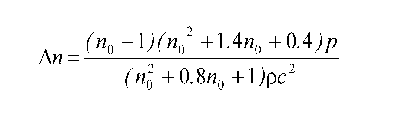
なお、音圧と屈折率変化の関係は古くから調べられており、水中超音波では、例えばEykmanの式が用いられる(M. F. J. Eykman, Rec. tray. chim. 14, 177-194 (1895)およびL. Adler and E. A. Hiedemann, J. Acoust. Soc. Amer. 34, 410 (1962)などを参照)。音速をc、音場がない場合の屈折率をn0、密度をρとして、音圧pの時の屈折率変化Δnは、次の式1に示すように、音圧の関数として表される。
1,21 屈折率センサ、2,22 光源部、3,23 光学バンドパスフィルタ、4,24 測定部、5,25 屈折率算出部、6 サーキュレータ、7 光ファイバ、8 誘電体多層膜、9 被測定物、10 キャビティ層、11 高屈折率層、12 低屈折率層、13 最上位層、14 スタブ、24A 検出部、24B 観測部
Claims (10)
- 光を出力する光源部と、
光伝送路の一端面に誘電体多層膜が形成されており、上記光伝送路と接している一端とは他端側の誘電体多層膜上に、所定の屈折率を有する被測定物が接しており、上記光伝送路を介して上記光源部から出力された光が入射される光学バンドパスフィルタと、
上記光学バンドパスフィルタに入射した光が上記被測定物で反射された反射光のスペクトルを測定する測定部と、
上記測定部で測定した反射光のスペクトルの中心波長に基づいて、上記反射光の屈折率を算出する屈折率算出部とを備え、
上記誘電体多層膜は、
略中央に配置されたキャビティ層と、
上記キャビティ層の両側に、複数の高屈折率層及び上記高屈折率層よりも屈折率が小さい複数の低屈折率層を積層した反射多層膜とを有し、
上記高屈折率層と上記低屈折率層とを合わせた光学的厚さは、上記光源部から出力された光の中心波長をλ0としたときにλ0/2であり、
上記高屈折率層及び上記低屈折率層の各層の光学的厚さは、それぞれλ0/4とは異なる値である屈折率センサ。 - 上記被測定物と接する上記高屈折率層又は上記低屈折率層の厚さが、他の上記高屈折率層及び上記低屈折率層の厚さに応じて異なる請求項1記載の屈折率センサ。
- 上記キャビティ層及び上記低屈折率層は、SiO2で構成され、厚さが225nmであり、
上記高屈折率層は、TiO2で構成され、厚さが225nmであり、
上記被測定物と接する上記高屈折率層又は上記低屈折率層の厚さが、他の上記高屈折率層及び上記低屈折率層の厚さに対して1.7倍以上である請求項2記載の屈折率センサ。 - 上記誘電体多層膜における上記キャビティ層と上記高屈折率層と上記低屈折率層との合計が25層以上である請求項3記載の屈折率センサ。
- 光を出力する出力ステップと、
光伝送路の一端面に誘電体多層膜が形成されており、上記光伝送路と接している一端とは他端側の誘電体多層膜上に、所定の屈折率を有する被測定物が接している光学バンドパスフィルタに、上記出力ステップで出力された光を上記光伝送路を介して入射させる入射ステップと、
上記入射ステップで上記光学バンドパスフィルタに入射した光が上記被測定物で反射された反射光のスペクトルを測定する測定ステップと、
上記測定ステップで測定した反射光のスペクトルの中心波長に基づいて、上記反射光の屈折率を算出する屈折率算出ステップとを有し、
上記誘電体多層膜は、
略中央に配置されたキャビティ層と、
上記キャビティ層の両側に、複数の高屈折率層及び上記高屈折率層よりも屈折率が小さい複数の低屈折率層を積層した反射多層膜とを有し、
上記高屈折率層と上記低屈折率層とを合わせた光学的厚さは、上記光源部から出力された光の中心波長をλ0としたときにλ0/2であり、
上記高屈折率層及び上記低屈折率層の各層の光学的厚さは、それぞれλ0/4とは異なる値である屈折率測定方法。 - 光伝送路の一端面に誘電体多層膜が形成されており、上記光伝送路と接している一端とは他端側の誘電体多層膜上に、所定の屈折率を有する被測定物が接する光学バンドパスフィルタと、
上記光学バンドパスフィルタの中心波長近傍の波長の光を出力して上記光伝送路を介して入射させる光源部と、
上記光学バンドパスフィルタに入射した光が上記被測定物で反射されて戻ってくる反射光の光パワーを電気信号に変換して検出する検出部と、
上記検出部により検出出力として得られる上記電気信号により示される上記反射光の光パワーに基づいて上記反射光の屈折率を算出する屈折率算出部とを備え、
上記誘電体多層膜は、
略中央に配置されたキャビティ層と、
上記キャビティ層の両側に、複数の高屈折率層及び上記高屈折率層よりも屈折率が小さい複数の低屈折率層を積層した反射多層膜とを有し、
上記高屈折率層と上記低屈折率層とを合わせた光学的厚さは、上記光源部から出力された光の中心波長をλ0としたときにλ0/2であり、
上記高屈折率層及び上記低屈折率層の各層の光学的厚さは、それぞれλ0/4とは異なる値である屈折率センサ。 - 上記被測定物と接する上記高屈折率層又は上記低屈折率層の厚さが、他の上記高屈折率層及び上記低屈折率層の厚さに応じて異なる請求項6記載の屈折率センサ。
- 上記キャビティ層及び上記低屈折率層は、SiO2で構成され、厚さが225nmであり、
上記高屈折率層は、TiO2で構成され、厚さが225nmであり、
上記被測定物と接する上記高屈折率層又は上記低屈折率層の厚さが、他の上記高屈折率層及び上記低屈折率層の厚さに対して1.7倍以上である請求項7記載の屈折率センサ。 - 上記誘電体多層膜における上記キャビティ層と上記高屈折率層と上記低屈折率層との合計が25層以上である請求項8記載の屈折率センサ。
- 光伝送路の一端面に誘電体多層膜が形成されており、上記光伝送路と接している一端とは他端側の誘電体多層膜上に、所定の屈折率を有する被測定物が接する光学バンドパスフィルタの中心波長近傍の波長の光を上記光伝送路を介して入射させる入射ステップと、
上記光学バンドパスフィルタに入射した光が上記被測定物で反射されて戻ってくる反射光の光パワーを電気信号に変換して検出する検出ステップと、
上記検出ステップにより検出出力として得られる上記電気信号により示される上記反射光の光パワーに基づいて上記反射光の屈折率を算出する屈折率算出ステップとを有し、
上記誘電体多層膜は、
略中央に配置されたキャビティ層と、
上記キャビティ層の両側に、複数の高屈折率層及び上記高屈折率層よりも屈折率が小さい複数の低屈折率層を積層した反射多層膜とを有し、
上記高屈折率層と上記低屈折率層とを合わせた光学的厚さは、上記光源部から出力された光の中心波長をλ0としたときにλ0/2であり、
上記高屈折率層及び上記低屈折率層の各層の光学的厚さは、それぞれλ0/4とは異なる値である屈折率測定方法。
Applications Claiming Priority (4)
| Application Number | Priority Date | Filing Date | Title |
|---|---|---|---|
| JP2011249902 | 2011-11-15 | ||
| JP2011-249902 | 2011-11-15 | ||
| JP2012-178970 | 2012-08-10 | ||
| JP2012178970A JP2013253953A (ja) | 2011-11-15 | 2012-08-10 | 屈折率センサ |
Publications (1)
| Publication Number | Publication Date |
|---|---|
| WO2013073435A1 true WO2013073435A1 (ja) | 2013-05-23 |
Family
ID=48429498
Family Applications (1)
| Application Number | Title | Priority Date | Filing Date |
|---|---|---|---|
| PCT/JP2012/078872 Ceased WO2013073435A1 (ja) | 2011-11-15 | 2012-11-07 | 屈折率センサ |
Country Status (2)
| Country | Link |
|---|---|
| JP (1) | JP2013253953A (ja) |
| WO (1) | WO2013073435A1 (ja) |
Cited By (1)
| Publication number | Priority date | Publication date | Assignee | Title |
|---|---|---|---|---|
| CN110895253A (zh) * | 2019-12-24 | 2020-03-20 | 费勉仪器科技(上海)有限公司 | 一种高效高分辨率的反光电子能谱实现装置 |
Families Citing this family (1)
| Publication number | Priority date | Publication date | Assignee | Title |
|---|---|---|---|---|
| CN105044031B (zh) * | 2015-08-31 | 2017-07-28 | 北京市煤炭矿用机电设备技术开发有限公司 | 利用光波导微环谐振器测试甲烷浓度的测试装置及方法 |
Citations (1)
| Publication number | Priority date | Publication date | Assignee | Title |
|---|---|---|---|---|
| JP2007101547A (ja) * | 2005-09-30 | 2007-04-19 | General Electric Co <Ge> | 光ファイバ化学物質感知装置、システム及び方法 |
Family Cites Families (3)
| Publication number | Priority date | Publication date | Assignee | Title |
|---|---|---|---|---|
| US8142723B2 (en) * | 2004-05-03 | 2012-03-27 | Chromologic, LLC | Tag free bio sensing micro strip |
| JP4226048B2 (ja) * | 2007-08-09 | 2009-02-18 | 株式会社渡辺製作所 | 光ファイバ圧力センサ |
| WO2011016775A1 (en) * | 2009-08-03 | 2011-02-10 | Nitto Denko Corporation | A sensor element |
-
2012
- 2012-08-10 JP JP2012178970A patent/JP2013253953A/ja active Pending
- 2012-11-07 WO PCT/JP2012/078872 patent/WO2013073435A1/ja not_active Ceased
Patent Citations (1)
| Publication number | Priority date | Publication date | Assignee | Title |
|---|---|---|---|---|
| JP2007101547A (ja) * | 2005-09-30 | 2007-04-19 | General Electric Co <Ge> | 光ファイバ化学物質感知装置、システム及び方法 |
Non-Patent Citations (4)
| Title |
|---|
| KYUNGSU KIM ET AL.: "High-Speed Measurements of Refractive Index Using Dielectric Multilayer Films Deposited on Optical Fiber End", EXTENDED ABSTRACTS OF THE 59TH SPRING MEETING; THE JAPAN SOCIETY OF APPLIED PHYSICS AND THE RELATED SOCIETIES, 29 February 2012 (2012-02-29), pages 05 - 139 * |
| KYUNGSU KIM ET AL.: "Refractive index sensor for liquids and solids using dielectric multilayer films deposited on optical fiber end surface", IEICE TECHNICAL REPORT, vol. 111, no. 69, 19 May 2011 (2011-05-19), pages 43 - 48 * |
| SEIICHI ONODA ET AL.: "Discrete Fiber Sensor Head using Fiber-stub", PROCEEDINGS OF THE IEICE SOCIETY CONFERENCE, VOL.2008 ELECTRONICS, vol. 2008, no. 2, 2 September 2008 (2008-09-02), pages 11 * |
| SEIICHI ONODA ET AL.: "Proposal of Temperature Sensing by BOF(BPFOn Fiber-end)", PROCEEDINGS OF THE IEICE GENERAL CONFERENCE, VOL.2007 ELECTRONICS, vol. 2007, no. 2, 7 March 2007 (2007-03-07), pages 14 * |
Cited By (1)
| Publication number | Priority date | Publication date | Assignee | Title |
|---|---|---|---|---|
| CN110895253A (zh) * | 2019-12-24 | 2020-03-20 | 费勉仪器科技(上海)有限公司 | 一种高效高分辨率的反光电子能谱实现装置 |
Also Published As
| Publication number | Publication date |
|---|---|
| JP2013253953A (ja) | 2013-12-19 |
Similar Documents
| Publication | Publication Date | Title |
|---|---|---|
| Iga et al. | Hetero-core structured fiber optic surface plasmon resonance sensor with silver film | |
| CN102323239B (zh) | 一种基于非对称双芯光纤的折射率传感器 | |
| CN101696933A (zh) | 一种基于谐振干涉复合结构和游标效应的光波导传感器 | |
| CN113218913B (zh) | 一种温度补偿的测量溶液浓度啁啾光纤光栅传感器 | |
| Taya et al. | Goos–Hänchen shift as a probe in evanescent slab waveguide sensors | |
| CN111323059A (zh) | 基于光纤布拉格光栅法布里-泊罗腔的传感装置 | |
| CN103335985B (zh) | 准分布式光纤光栅表面等离子体共振传感器及制备方法 | |
| US10466096B2 (en) | Fiber optic hydrophone sensors and uses thereof | |
| CN103697921A (zh) | 一种光纤传感头和基于该传感头的测量应变、应力和压力的光纤传感系统及方法 | |
| CN110530466B (zh) | 基于双无芯光纤级联的强度调制型液位传感检测方法 | |
| WO2013073435A1 (ja) | 屈折率センサ | |
| CN115164956B (zh) | 一种颜色和模场协同编码的分布式光纤传感装置 | |
| US9945740B2 (en) | Two wavelength optical interferometric pressure switch and pressure transducers | |
| CN114964331B (zh) | 一种光纤多元参量检测系统及方法 | |
| CN108318452A (zh) | 一种强度调制型四锥光纤湿度传感器 | |
| CN101738215B (zh) | 一种基于多次反射的双光束脉冲干涉法 | |
| FR3052923A1 (fr) | Reflecteur optique resonant a multiples couches minces de materiaux dielectriques, capteur optique et dispositif d'amplification laser comportant un tel reflecteur | |
| CN110057439A (zh) | 一种基于f-p干涉的低谐振偏心光纤声敏传感装置 | |
| CN103697920A (zh) | 一种光纤传感头和基于该传感头的测量液体折射率的光纤传感系统及方法 | |
| EP3973256B1 (fr) | Capteur acoustique à fibre optique et système de mesure, véhicule et procédé de mesure associés | |
| JP2008039787A (ja) | 光ファイバ圧力センサ | |
| Apriyanto et al. | A multimode fiber refractive index sensor | |
| CN114324241A (zh) | 基于伪表面等离激元三维堆叠结构的传感器 | |
| CN1323980A (zh) | 一种基于楔形法布里-珀罗干涉滤光片的光波长测量技术 | |
| JPH0345328B2 (ja) |
Legal Events
| Date | Code | Title | Description |
|---|---|---|---|
| 121 | Ep: the epo has been informed by wipo that ep was designated in this application |
Ref document number: 12849373 Country of ref document: EP Kind code of ref document: A1 |
|
| NENP | Non-entry into the national phase |
Ref country code: DE |
|
| 122 | Ep: pct application non-entry in european phase |
Ref document number: 12849373 Country of ref document: EP Kind code of ref document: A1 |