WO2013027838A1 - 色素増感太陽電池及び増感色素 - Google Patents
色素増感太陽電池及び増感色素 Download PDFInfo
- Publication number
- WO2013027838A1 WO2013027838A1 PCT/JP2012/071505 JP2012071505W WO2013027838A1 WO 2013027838 A1 WO2013027838 A1 WO 2013027838A1 JP 2012071505 W JP2012071505 W JP 2012071505W WO 2013027838 A1 WO2013027838 A1 WO 2013027838A1
- Authority
- WO
- WIPO (PCT)
- Prior art keywords
- group
- dye
- solar cell
- sensitized solar
- tert
- Prior art date
- Legal status (The legal status is an assumption and is not a legal conclusion. Google has not performed a legal analysis and makes no representation as to the accuracy of the status listed.)
- Ceased
Links
- 0 C*c(cc(*)cc1)c1-c1ccc(C=C(C(O)=O)C#N)[s]1 Chemical compound C*c(cc(*)cc1)c1-c1ccc(C=C(C(O)=O)C#N)[s]1 0.000 description 3
- XQQBUAPQHNYYRS-UHFFFAOYSA-N Cc1ccc[s]1 Chemical compound Cc1ccc[s]1 XQQBUAPQHNYYRS-UHFFFAOYSA-N 0.000 description 2
- YTZTWRBGMXYCEH-UHFFFAOYSA-N CC1SC(C)=CN1 Chemical compound CC1SC(C)=CN1 YTZTWRBGMXYCEH-UHFFFAOYSA-N 0.000 description 1
- BPWYNWSOQOXOPI-UHFFFAOYSA-N COc(cc1OC)cc(OC)c1Br Chemical compound COc(cc1OC)cc(OC)c1Br BPWYNWSOQOXOPI-UHFFFAOYSA-N 0.000 description 1
- RDNKTTBSNXARLZ-JTQLQIEISA-N C[C@@H]1C(c(c(OC)cc(OC)c2)c2OC)=CC=C1C=O Chemical compound C[C@@H]1C(c(c(OC)cc(OC)c2)c2OC)=CC=C1C=O RDNKTTBSNXARLZ-JTQLQIEISA-N 0.000 description 1
- WEOCBJMQLLMFGY-UHFFFAOYSA-N Cc([s]c(C)c1OC)c1OC Chemical compound Cc([s]c(C)c1OC)c1OC WEOCBJMQLLMFGY-UHFFFAOYSA-N 0.000 description 1
- WSXSIQXFVQCFLZ-UHFFFAOYSA-N Cc1c2OCCOc2c(C)[s]1 Chemical compound Cc1c2OCCOc2c(C)[s]1 WSXSIQXFVQCFLZ-UHFFFAOYSA-N 0.000 description 1
Images
Classifications
-
- H—ELECTRICITY
- H01—ELECTRIC ELEMENTS
- H01G—CAPACITORS; CAPACITORS, RECTIFIERS, DETECTORS, SWITCHING DEVICES, LIGHT-SENSITIVE OR TEMPERATURE-SENSITIVE DEVICES OF THE ELECTROLYTIC TYPE
- H01G9/00—Electrolytic capacitors, rectifiers, detectors, switching devices, light-sensitive or temperature-sensitive devices; Processes of their manufacture
- H01G9/20—Light-sensitive devices
- H01G9/2059—Light-sensitive devices comprising an organic dye as the active light absorbing material, e.g. adsorbed on an electrode or dissolved in solution
- H01G9/2063—Light-sensitive devices comprising an organic dye as the active light absorbing material, e.g. adsorbed on an electrode or dissolved in solution comprising a mixture of two or more dyes
-
- C—CHEMISTRY; METALLURGY
- C07—ORGANIC CHEMISTRY
- C07D—HETEROCYCLIC COMPOUNDS
- C07D277/00—Heterocyclic compounds containing 1,3-thiazole or hydrogenated 1,3-thiazole rings
- C07D277/02—Heterocyclic compounds containing 1,3-thiazole or hydrogenated 1,3-thiazole rings not condensed with other rings
- C07D277/20—Heterocyclic compounds containing 1,3-thiazole or hydrogenated 1,3-thiazole rings not condensed with other rings having two or three double bonds between ring members or between ring members and non-ring members
- C07D277/22—Heterocyclic compounds containing 1,3-thiazole or hydrogenated 1,3-thiazole rings not condensed with other rings having two or three double bonds between ring members or between ring members and non-ring members with only hydrogen atoms, hydrocarbon or substituted hydrocarbon radicals, directly attached to ring carbon atoms
- C07D277/30—Radicals substituted by carbon atoms having three bonds to hetero atoms with at the most one bond to halogen, e.g. ester or nitrile radicals
-
- C—CHEMISTRY; METALLURGY
- C07—ORGANIC CHEMISTRY
- C07D—HETEROCYCLIC COMPOUNDS
- C07D333/00—Heterocyclic compounds containing five-membered rings having one sulfur atom as the only ring hetero atom
- C07D333/02—Heterocyclic compounds containing five-membered rings having one sulfur atom as the only ring hetero atom not condensed with other rings
- C07D333/04—Heterocyclic compounds containing five-membered rings having one sulfur atom as the only ring hetero atom not condensed with other rings not substituted on the ring sulphur atom
- C07D333/06—Heterocyclic compounds containing five-membered rings having one sulfur atom as the only ring hetero atom not condensed with other rings not substituted on the ring sulphur atom with only hydrogen atoms, hydrocarbon or substituted hydrocarbon radicals, directly attached to the ring carbon atoms
- C07D333/24—Radicals substituted by carbon atoms having three bonds to hetero atoms with at the most one bond to halogen, e.g. ester or nitrile radicals
-
- C—CHEMISTRY; METALLURGY
- C09—DYES; PAINTS; POLISHES; NATURAL RESINS; ADHESIVES; COMPOSITIONS NOT OTHERWISE PROVIDED FOR; APPLICATIONS OF MATERIALS NOT OTHERWISE PROVIDED FOR
- C09B—ORGANIC DYES OR CLOSELY-RELATED COMPOUNDS FOR PRODUCING DYES, e.g. PIGMENTS; MORDANTS; LAKES
- C09B23/00—Methine or polymethine dyes, e.g. cyanine dyes
- C09B23/0008—Methine or polymethine dyes, e.g. cyanine dyes substituted on the polymethine chain
- C09B23/005—Methine or polymethine dyes, e.g. cyanine dyes substituted on the polymethine chain the substituent being a COOH and/or a functional derivative thereof
- C09B23/0058—Methine or polymethine dyes, e.g. cyanine dyes substituted on the polymethine chain the substituent being a COOH and/or a functional derivative thereof the substituent being CN
-
- C—CHEMISTRY; METALLURGY
- C09—DYES; PAINTS; POLISHES; NATURAL RESINS; ADHESIVES; COMPOSITIONS NOT OTHERWISE PROVIDED FOR; APPLICATIONS OF MATERIALS NOT OTHERWISE PROVIDED FOR
- C09B—ORGANIC DYES OR CLOSELY-RELATED COMPOUNDS FOR PRODUCING DYES, e.g. PIGMENTS; MORDANTS; LAKES
- C09B23/00—Methine or polymethine dyes, e.g. cyanine dyes
- C09B23/02—Methine or polymethine dyes, e.g. cyanine dyes the polymethine chain containing an odd number of >CH- or >C[alkyl]- groups
- C09B23/04—Methine or polymethine dyes, e.g. cyanine dyes the polymethine chain containing an odd number of >CH- or >C[alkyl]- groups one >CH- group, e.g. cyanines, isocyanines, pseudocyanines
-
- C—CHEMISTRY; METALLURGY
- C09—DYES; PAINTS; POLISHES; NATURAL RESINS; ADHESIVES; COMPOSITIONS NOT OTHERWISE PROVIDED FOR; APPLICATIONS OF MATERIALS NOT OTHERWISE PROVIDED FOR
- C09B—ORGANIC DYES OR CLOSELY-RELATED COMPOUNDS FOR PRODUCING DYES, e.g. PIGMENTS; MORDANTS; LAKES
- C09B57/00—Other synthetic dyes of known constitution
-
- C—CHEMISTRY; METALLURGY
- C09—DYES; PAINTS; POLISHES; NATURAL RESINS; ADHESIVES; COMPOSITIONS NOT OTHERWISE PROVIDED FOR; APPLICATIONS OF MATERIALS NOT OTHERWISE PROVIDED FOR
- C09B—ORGANIC DYES OR CLOSELY-RELATED COMPOUNDS FOR PRODUCING DYES, e.g. PIGMENTS; MORDANTS; LAKES
- C09B67/00—Influencing the physical, e.g. the dyeing or printing properties of dyestuffs without chemical reactions, e.g. by treating with solvents grinding or grinding assistants, coating of pigments or dyes; Process features in the making of dyestuff preparations; Dyestuff preparations of a special physical nature, e.g. tablets, films
- C09B67/0033—Blends of pigments; Mixtured crystals; Solid solutions
-
- H—ELECTRICITY
- H10—SEMICONDUCTOR DEVICES; ELECTRIC SOLID-STATE DEVICES NOT OTHERWISE PROVIDED FOR
- H10K—ORGANIC ELECTRIC SOLID-STATE DEVICES
- H10K85/00—Organic materials used in the body or electrodes of devices covered by this subclass
- H10K85/60—Organic compounds having low molecular weight
- H10K85/649—Aromatic compounds comprising a hetero atom
- H10K85/652—Cyanine dyes
-
- H—ELECTRICITY
- H10—SEMICONDUCTOR DEVICES; ELECTRIC SOLID-STATE DEVICES NOT OTHERWISE PROVIDED FOR
- H10K—ORGANIC ELECTRIC SOLID-STATE DEVICES
- H10K85/00—Organic materials used in the body or electrodes of devices covered by this subclass
- H10K85/60—Organic compounds having low molecular weight
- H10K85/649—Aromatic compounds comprising a hetero atom
- H10K85/655—Aromatic compounds comprising a hetero atom comprising only sulfur as heteroatom
-
- H—ELECTRICITY
- H01—ELECTRIC ELEMENTS
- H01G—CAPACITORS; CAPACITORS, RECTIFIERS, DETECTORS, SWITCHING DEVICES, LIGHT-SENSITIVE OR TEMPERATURE-SENSITIVE DEVICES OF THE ELECTROLYTIC TYPE
- H01G9/00—Electrolytic capacitors, rectifiers, detectors, switching devices, light-sensitive or temperature-sensitive devices; Processes of their manufacture
- H01G9/20—Light-sensitive devices
- H01G9/2004—Light-sensitive devices characterised by the electrolyte, e.g. comprising an organic electrolyte
- H01G9/2013—Light-sensitive devices characterised by the electrolyte, e.g. comprising an organic electrolyte the electrolyte comprising ionic liquids, e.g. alkyl imidazolium iodide
-
- H—ELECTRICITY
- H01—ELECTRIC ELEMENTS
- H01G—CAPACITORS; CAPACITORS, RECTIFIERS, DETECTORS, SWITCHING DEVICES, LIGHT-SENSITIVE OR TEMPERATURE-SENSITIVE DEVICES OF THE ELECTROLYTIC TYPE
- H01G9/00—Electrolytic capacitors, rectifiers, detectors, switching devices, light-sensitive or temperature-sensitive devices; Processes of their manufacture
- H01G9/20—Light-sensitive devices
- H01G9/2027—Light-sensitive devices comprising an oxide semiconductor electrode
- H01G9/2031—Light-sensitive devices comprising an oxide semiconductor electrode comprising titanium oxide, e.g. TiO2
-
- H—ELECTRICITY
- H10—SEMICONDUCTOR DEVICES; ELECTRIC SOLID-STATE DEVICES NOT OTHERWISE PROVIDED FOR
- H10K—ORGANIC ELECTRIC SOLID-STATE DEVICES
- H10K85/00—Organic materials used in the body or electrodes of devices covered by this subclass
- H10K85/30—Coordination compounds
- H10K85/341—Transition metal complexes, e.g. Ru(II)polypyridine complexes
- H10K85/344—Transition metal complexes, e.g. Ru(II)polypyridine complexes comprising ruthenium
-
- Y—GENERAL TAGGING OF NEW TECHNOLOGICAL DEVELOPMENTS; GENERAL TAGGING OF CROSS-SECTIONAL TECHNOLOGIES SPANNING OVER SEVERAL SECTIONS OF THE IPC; TECHNICAL SUBJECTS COVERED BY FORMER USPC CROSS-REFERENCE ART COLLECTIONS [XRACs] AND DIGESTS
- Y02—TECHNOLOGIES OR APPLICATIONS FOR MITIGATION OR ADAPTATION AGAINST CLIMATE CHANGE
- Y02E—REDUCTION OF GREENHOUSE GAS [GHG] EMISSIONS, RELATED TO ENERGY GENERATION, TRANSMISSION OR DISTRIBUTION
- Y02E10/00—Energy generation through renewable energy sources
- Y02E10/50—Photovoltaic [PV] energy
- Y02E10/542—Dye sensitized solar cells
-
- Y—GENERAL TAGGING OF NEW TECHNOLOGICAL DEVELOPMENTS; GENERAL TAGGING OF CROSS-SECTIONAL TECHNOLOGIES SPANNING OVER SEVERAL SECTIONS OF THE IPC; TECHNICAL SUBJECTS COVERED BY FORMER USPC CROSS-REFERENCE ART COLLECTIONS [XRACs] AND DIGESTS
- Y02—TECHNOLOGIES OR APPLICATIONS FOR MITIGATION OR ADAPTATION AGAINST CLIMATE CHANGE
- Y02E—REDUCTION OF GREENHOUSE GAS [GHG] EMISSIONS, RELATED TO ENERGY GENERATION, TRANSMISSION OR DISTRIBUTION
- Y02E10/00—Energy generation through renewable energy sources
- Y02E10/50—Photovoltaic [PV] energy
- Y02E10/549—Organic PV cells
Definitions
- the present invention relates to a dye-sensitized solar cell, and more particularly to a dye-sensitized solar cell and a sensitizing dye having high photoelectric conversion efficiency.
- Solar cells that can efficiently convert sunlight into electricity and are currently in practical use include residential single crystal silicon, polycrystalline silicon, amorphous silicon, and inorganic solar cells such as cadmium telluride and indium copper selenide A battery is mentioned. Disadvantages of these inorganic solar cells include, for example, that silicon having a very high purity is required, the purification process is complicated, the number of processes is large, and the manufacturing cost is high.
- Non-patent Document 1 a porous semiconductor layer such as titanium oxide adsorbing a sensitizing dye and a carrier transport layer are laminated between a transparent electrode and a counter electrode formed on two light-transmitting substrates such as glass. ing. Sunlight enters from the light-transmitting substrate, passes through the transparent electrode, reaches the semiconductor layer, and excites the sensitizing dye.
- the generated excited electrons move to the transparent electrode via the semiconductor layer, and further return to the counter electrode via the external electric circuit, and are transported by the ions in the carrier transport layer in the battery to the oxidized dye. Return.
- sunlight energy is converted into electric energy.
- a ruthenium pyridine complex is used, and there are N719 and N3 of bipyridine complexes, a black dye of terpyridine complex, and the like.
- N719 has a wide absorption wavelength range of 300 to 730 nm and a black die of 300 to 860 nm, but generally has a low molar extinction coefficient and a photoelectric conversion efficiency of only about 9%.
- the wavelength band of light absorbed by the sensitizing dye can be expanded so that sunlight in a wide range of wavelengths from ultraviolet light to infrared light can be used, or A measure such as increasing the amount of the sensitizing dye adsorbed on the semiconductor surface to absorb more light may be adopted.
- the former method two or more types of sensitizing dyes having different absorption peak wavelengths or two or more types of sensitizing dyes exhibiting the maximum counter-incident photon yield in different absorption wavelength regions are selected, and Techniques that broaden the absorption wavelength band of sensitizing dyes by mixing them and adsorbing them on the semiconductor surface, or by adsorbing different dyes in layers are disclosed (Patent Documents 1 to 4).
- Patent Documents 1 to 4 a similar organic dye having a similar structure but different molecular sizes is mixed and adsorbed on the semiconductor surface. In this way, the small pigment is adsorbed so as to fill the gap where the large pigment is adsorbed.
- the photoelectric conversion efficiency of the conventional dye-sensitized solar cell adopting the above-mentioned measures is about 7 to 9%, which is not much different from the efficiency when the ruthenium pyridine complex is used alone as the sensitizing dye.
- the additive effect or synergistic effect of the respective characteristics of the two kinds of adsorbing dyes is not obtained.
- a dye-sensitized solar cell in which a black dye of a ruthenium pyridine complex and an organic dye D-131 are mixed and adsorbed exhibits excellent photoelectric conversion efficiency (11.0%) (Non-patent Document 2).
- the certified photoelectric conversion efficiency (11.1%) of a dye-sensitized solar cell using a black die alone could not be exceeded.
- An object of the present invention is to provide a dye-sensitized solar cell having excellent photoelectric conversion efficiency by selecting a combination of dyes that can utilize the respective characteristics when two kinds of dyes are mixed and adsorbed on a semiconductor. is there.
- a dye-sensitized solar cell provided with the following (a) to (e) is provided.
- A A conductive support.
- B A porous semiconductor layer.
- C Two types of sensitizing dyes adsorbed on the porous semiconductor layer, having different molecular sizes, and at least one having at least one alkyl side chain in the molecule.
- D Carrier transport layer.
- E Counter electrode.
- At least one of the two types of sensitizing dyes may have a photoelectric conversion characteristic open-circuit voltage of 0.65 V or more.
- a dye-sensitized solar cell provided with the following (a) to (e) is provided.
- A A conductive support.
- B A porous semiconductor layer.
- C Two types of sensitizing dyes that are adsorbed on the porous semiconductor layer, have different molecular sizes, and at least one of them has a photoelectric conversion characteristic open-circuit voltage of 0.65 V or more.
- D Carrier transport layer.
- E Counter electrode.
- At least one of the two kinds of sensitizing dyes may have at least one alkyl side chain in the molecule.
- the molecular weight of the smaller molecular size of the two types of sensitizing dyes may be 400 or less.
- At least one of the two kinds of sensitizing dyes may have at least one alkyl side chain in the molecule.
- the sensitizing dye having the smaller molecular size of the two kinds of sensitizing dyes may be an organic dye represented by the following formula.
- R 1 to R 5 are each independently a hydrogen atom, an alkyl group having 1 to 18 carbon atoms, an alkoxy group, a dialkylamino group, or an alicyclic amino group, and the ⁇ -spacer is substituted
- at least one of R 1 to R 5 may be an alkoxy group having an alkyl side chain portion having 3 to 16 carbon atoms, a dialkylamino group, or an alicyclic amino group.
- the alkyl side chain moiety is a methyl group, ethyl group, propyl group, butyl group, pentyl group, hexyl group, heptyl group, octyl group, hexadecyl group, isopropyl group, isobutyl group, isopentyl group, isohexyl group, isoheptyl group.
- isooctyl group, neopentyl group, neohexyl group, neoheptyl group, neooctyl group, sec-butyl group, sec-pentyl group, sec-hexyl group, sec-heptyl group, sec-octyl group, tert-butyl group, tert -Pentyl, tert-hexyl, tert-heptyl, tert-octyl, 2-ethylhexyl, and 1,1,3,3-tetramethylbutyl may be selected.
- the alicyclic amino group may be pyrrolidine or piperidine.
- the aromatic heterocyclic group may have any structure in the following formula.
- One of the two types of sensitizing dyes may be a ruthenium pyridine complex.
- One of the two types of sensitizing dyes may be a terpyridine ruthenium complex.
- a sensitizing dye represented by the above formula (1) is provided.
- R 1 to R 5 may be an alkoxy group having an alkyl side chain portion having 3 to 16 carbon atoms, a dialkylamino group, or an alicyclic amino group.
- the alkyl side chain moiety is a methyl group, ethyl group, propyl group, butyl group, pentyl group, hexyl group, heptyl group, octyl group, hexadecyl group, isopropyl group, isobutyl group, isopentyl group, isohexyl group, isoheptyl group.
- isooctyl group, neopentyl group, neohexyl group, neoheptyl group, neooctyl group, sec-butyl group, sec-pentyl group, sec-hexyl group, sec-heptyl group, sec-octyl group, tert-butyl group, tert -Pentyl, tert-hexyl, tert-heptyl, tert-octyl, 2-ethylhexyl, and 1,1,3,3-tetramethylbutyl may be selected.
- the alicyclic amino group may be pyrrolidine or piperidine.
- aromatic heterocyclic group may have any structure in the above formula (2).
- the present invention by mixing and adsorbing two types of dyes having different characteristics to the semiconductor, it is possible to absorb sunlight in a wide range of wavelengths, suppress the interaction between the dye molecules, and the dye adsorbed on the semiconductor surface.
- the excited electrons can be efficiently transferred to the conduction band of the semiconductor, and from the conduction band to the carrier transport layer.
- the reverse current flowing to the LUMO and HOMO of the dye is suppressed.
- the photoelectric conversion efficiency of the dye-sensitized solar cell in which two kinds of dyes are mixed and adsorbed on the porous semiconductor layer can be improved.
- the present inventors conducted earnest research to find a combination of dyes that can make use of each characteristic when two kinds of dyes having different molecular sizes are mixed and adsorbed on the surface of a porous semiconductor. As a result, it was found that a combination of a ruthenium pyridine complex and an organic dye satisfying certain conditions brings about an excellent photoelectric conversion efficiency of the dye-sensitized solar cell.
- titanium oxide paste (Solaronix, Tinanoxide T / SP) is screen-printed with a film thickness of about 20 ⁇ m and an area of about 5 mm ⁇ 5 mm. Then, it was applied on a transparent conductive film, pre-dried at 100 ° C. for 30 minutes, and then baked at 500 ° C. for 2 hours in an air atmosphere to produce a titanium oxide film having a thickness of 20 ⁇ m as a porous semiconductor layer. .
- a dye for screening was dissolved in ethanol to a concentration of 2 ⁇ 10 ⁇ 4 M and deoxycholic acid to a concentration of 2 ⁇ 10 ⁇ 2 M to prepare an adsorption solution.
- the glass plate was immersed in this solution for 24 hours to adsorb the dye to the porous semiconductor layer.
- a counter electrode was prepared by depositing 1 ⁇ m of a platinum film on the glass substrate, facing the porous semiconductor layer adsorbed with the dye, and tightly sealed with a thermal compression film spacer interposed between them to prevent short circuit.
- electrolytes such as 1,2-dimethyl-3-propylimidazolium iodide (0.6M), lithium iodide (0.1M), iodine (0.05M), and 4-tert- A solar cell was fabricated by injecting an acetonitrile solution of butylpyridine (0.5M) to form a carrier transport layer.
- the obtained solar cell was irradiated with light having an intensity of 100 mWcm ⁇ 2 (AM1.5, solar simulator), and current-voltage characteristics were measured.
- the selected dye and a dye having a different molecular size were mixed and adsorbed on a porous semiconductor, the photoelectric conversion characteristics were measured, and a combination in which the characteristics of each dye were utilized was searched.
- the dye may have at least one alkyl side chain in the molecule.
- the molecular weight of the dye having the smaller molecular size may be 400 or less.
- dye shows independently may be made to be 0.6V or more, It discovered that 0.65V or more was especially preferable.
- sensitizing dye I is preferably a ruthenium pyridine complex, and N3 (formula (3)) and N719 (formula (4)) of a bipyridine complex. ) And black dyes of terpyridine complexes (formula (5)) are more preferred.
- a sensitizing dye II which is not a ruthenium complex and exhibits an open circuit voltage of 0.65 V or more among two kinds of dyes having different molecular sizes
- a sensitizing dye II which is not a ruthenium complex and exhibits an open circuit voltage of 0.65 V or more among two kinds of dyes having different molecular sizes
- the following formula (6 )) (Non-patent document 3), (formula (7)) compound (non-patent document 4), (formula (8)) compound (non-patent document 5), (formula (9)) compound (Non-patent document 6), (Formula (10)) compound (Non-patent document 7), (Formula (11)) compound (Non-patent document 8), (Formula (12)) compound (Non-patent document 9) ), A compound of formula (13) (non-patent document 10)), a compound of formula (14) (non-patent document 11), a compound of formula (15) (non-patent document
- the alkyl side chain is a linear or branched alkyl group (for example, the above formula (7 )), (Compounds of formula (12)) and (formula (13)), alkoxy groups (eg, compounds of formulas (6) and (9) above), monoalkylamino groups, dialkylamino It is bonded to the mother nucleus of the dye as a group, and there may be an ether bond, a thioether bond or an amino bond in the alkyl chain.
- the number of carbon atoms is 1 to 18, preferably 3 to 16, and particularly preferably 4 to 8.
- alkyl side chain examples include, for example, methyl group, ethyl group, propyl group, butyl group, pentyl group, hexyl group, heptyl group, octyl group, hexadecyl group, isopropyl group, isobutyl group, isopentyl group, isohexyl group, Isoheptyl group, isooctyl group, neopentyl group, neohexyl group, neoheptyl group, neooctyl group, sec-butyl group, sec-pentyl group, sec-hexyl group, sec-heptyl group, sec-octyl group, tert-butyl Group, tert-pentyl group, tert-hexyl group, tert-heptyl group, tert-octyl group, 2-ethyl
- Such an alkyl side chain prevents association between the dyes, and a hydrophobic layer is formed between the semiconductor surface and the carrier transport layer, so that the electrolyte in the carrier transport layer is less likely to be eroded.
- the reverse current flowing between the transport layers can be suppressed.
- Examples of the dye having a smaller molecular size include an organic dye having an open circuit voltage of 0.65 V or more, an alkyl side chain in the molecule, and a molecular weight of 400 or less. There are organic dyes represented by the general formula (formula (16)).
- This sensitizing dye II has a general formula (formula (16) in which 2-cyanoacrylic acid having a carboxyl group as an anchor group and a nitrile group as an auxiliary group in its molecule is used as an acceptor site in order to be strongly adsorbed on the semiconductor surface. )) Represented by a [donor moiety- ( ⁇ -spacer) -acceptor moiety] type organic dye, wherein R 1 to R 5 are each independently a hydrogen atom, an alkyl group having 1 to 18 carbon atoms, In the alkoxy group, dialkylamino group, and alicyclic amino group, the alkyl side chain portion of each functional group preferably has 4 to 16 carbon atoms.
- alkyl groups such as hexyl group, tert-heptyl group, tert-octyl group, 2-ethylhexyl group, 1,1,3,3-t
- the ⁇ -spacer moiety represents an optionally substituted aromatic heterocyclic group such as a divalent phenylene group, thiophene or thiazole. Specific examples are shown below.
- the sensitizing dye II represented by the general formula (formula (16)) may have a molecular weight of 400 or less, and a gap formed by adsorbing a large molecular size dye (that is, the sensitizing dye I) on the semiconductor surface.
- the molecular size can be made small enough to fill and adsorb.
- the LUMO of the dye is in the vicinity of the carboxyl group, in the acrylic acid part, and HOMO is in the terminal phenyl group part. Therefore, the electron distribution in the excited state has the highest electron density in the vicinity of the carboxyl group, and the excited electrons are efficiently injected into the semiconductor.
- the energy gap between the LUMO level, the HOMO level, and the conduction band level of the semiconductor is increased, and the reverse current in which excited electrons injected from the dye into the semiconductor return to the LUMO or HOMO of the dye. Can be prevented.
- the small dyes are absorbed in the gaps where the large size dyes are adsorbed, so the portion of the semiconductor surface that is not coated with the dyes decreases.
- the reverse current in which excited electrons injected from the dye flow from the semiconductor surface to the carrier transport layer is suppressed.
- the method for synthesizing the dye represented by the general formula (formula (16)) of the present invention is not particularly limited.
- boronic acid of benzene substituted with an alkyl group, an alkoxy group or an amino group and 5-bromothiophene-2 Carboaldehyde can be synthesized by cross-coupling by Suzuki reaction and then condensing aldehyde and cyanoacetic acid by Knoevenagel reaction.
- the brominated product of the substituted benzene and 2-thiopheneboronic acid are cross-coupled by the Suzuki reaction, then the formyl group is introduced by the Vilsmeier reaction, and finally the aldehyde and cyanoacetic acid are converted by the Knoevenagel reaction. It can also be synthesized by condensation.
- the dye-sensitized solar cell of the present invention is formed by sequentially laminating a porous semiconductor layer adsorbing a sensitizing dye, a carrier transporting layer, and a counter electrode on a conductive support, and the sensitizing dye includes two different types. It consists of a dye, and the porous semiconductor consists of titanium oxide.
- the support itself may be conductive like metal.
- a support such as glass or plastic having a conductive layer on the surface can be used.
- preferred conductive materials for the conductive layer include metals such as gold, platinum, silver, copper, aluminum, and indium, conductive carbon, indium-tin oxide, tin oxide doped with fluorine, etc.
- a conductive layer can be formed on a support by a usual method.
- the thickness of these conductive layers is preferably about 0.02 to 5 ⁇ m.
- the surface resistance is preferably 40 ⁇ / sq or less.
- the conductive support is a light receiving surface, it is preferably transparent.
- the film thickness of an electroconductive support body will not be specifically limited if appropriate intensity
- a laminate in which a conductive layer made of tin oxide doped with fluorine is laminated on a transparent substrate made of soda-lime float glass can be used as a typical support.
- a transparent polymer sheet provided with the conductive layer may be used.
- the transparent polymer sheet include tetraacetylcellulose, polyethylene terephthalate, polyphenylene sulfide, polycarbonate, polyarylate, polyetherimide, and phenoxy resin.
- a metal lead wire may be added to reduce the resistance of the transparent substrate.
- platinum, copper, aluminum, indium, nickel or the like is preferable.
- the metal lead wire may be installed on a transparent substrate by sputtering, vapor deposition, or the like, and a transparent conductive film such as tin oxide or ITO may be provided thereon.
- the porous semiconductor layer is composed of an aggregate of semiconductor fine particles, and any semiconductor fine particles that are generally used for photoelectric conversion materials can be used.
- any semiconductor fine particles that are generally used for photoelectric conversion materials can be used.
- titanium oxide, zinc oxide, tin oxide, iron oxide, niobium oxide, zirconium oxide, cerium oxide, tungsten oxide, silicon oxide, aluminum oxide, nickel oxide, barium titanate, strontium titanate, cadmium sulfide, lead sulfide, sulfide Zinc, indium phosphide, copper-indium sulfide, etc. may be used alone or in combination.
- titanium oxide, zinc oxide, tin oxide, and niobium oxide are preferable, and titanium oxide is particularly preferable from the viewpoint of stability and safety.
- titanium oxide was used as a material for the semiconductor fine particles.
- Crystalline titanium oxide has two types of crystal forms, anatase type and rutile type, which can take any form depending on the production method and thermal history, but a mixture of these is common.
- the material of the semiconductor fine particles is preferably an anatase type from the viewpoint of photocatalytic activity, and even a mixture having an anatase type content of 90% or more is preferable.
- the anatase-type titanium oxide may be a commercially available powder, sol, or slurry, or may be prepared with a predetermined particle diameter by known methods described in various documents.
- the particle size of the semiconductor fine particles is not particularly limited, but fine powder (average particle size is 1 nm to 1 ⁇ m) is preferable. Further, two or more kinds of particles having different particle diameters may be mixed and used. In this case, the average particle size ratio should have a difference of 10 times or more. Particles having a large particle size (preferably 100 to 500 nm) have the effect of scattering incident light and increasing the quantum yield. In addition, particles having a small particle size (preferably 5 to 50 nm) have the effect of increasing the number of adsorption points and improving dye adsorption.
- the method for forming the porous semiconductor layer is not particularly limited, and a known method may be used.
- coating the suspension containing a semiconductor fine particle on a transparent conductive film, and drying and baking is mentioned.
- the solvent for suspending the semiconductor fine particles include ethylene glycol monomethyl ether, isopropyl alcohol, isopropyl alcohol-toluene mixed solvent, water and the like.
- a commercially available titanium oxide paste may be used instead of the suspension.
- Application to the substrate can be performed by various methods such as a known dipping method, spray method, wire bar method, spin coating method, roller coating method, blade coating method, gravure coating method, and screen printing.
- the drying, firing temperature, time, atmosphere, and the like can be adjusted according to the types of the substrate and semiconductor fine particles. Usually, it is carried out at 40 to 700 ° C. under atmospheric pressure for about 10 minutes to 10 hours. Moreover, you may repeat the process of application
- the porous semiconductor layer has a large surface area and a large thickness of the semiconductor layer so that a large amount of dye can be adsorbed, so that the amount of supported dye increases.
- the surface area is preferably about 10 to 200 m 2 / g and the thickness is preferably about 0.1 to 100 ⁇ m.
- a method of adsorbing the sensitizing dye to the porous semiconductor As a method of adsorbing the sensitizing dye to the porous semiconductor, a method of immersing the semiconductor electrode in a solution in which the sensitizing dye is dissolved is general.
- the solvent of the dye solution include organic solvents such as alcohol, toluene, acetonitrile, tetrahydrofuran, chloroform, dimethylformamide, and two or more kinds of solvents may be mixed in order to increase solubility.
- the concentration of the dye in the solvent is appropriately adjusted according to the type of the sensitizing dye and the solvent, but is preferably about 0.01 to 10 mM. If necessary, deoxycholic acid or the like may be added to reduce association of the dye molecules.
- the immersion time is appropriately adjusted according to the sensitizing dye used, the type of solvent, the concentration of the solution, etc., but is preferably 2 to 50 hours, and the temperature during immersion is preferably 10 to 50 ° C. Immersion may be performed once or a plurality of times. Also, when the amount of dye adsorbed is large, the dye that is not directly bonded to the semiconductor will be released to the carrier transport layer of the solar cell and cause a decrease in photoelectric conversion efficiency. It is preferred to wash to remove unadsorbed dye. Examples of the cleaning agent include methanol, ethanol, acetonitrile, acetone, and the like, which have relatively high volatility.
- the surface of the semiconductor may be treated with an organic basic compound in order to make the adsorption state of the dye more stable, thereby promoting the removal of the unadsorbed dye.
- organic basic compound include derivatives such as pyridine and quinoline. When these compounds are liquid, they may be used as they are, but when they are solid, they may be dissolved in the same solvent as the dye solution.
- two kinds of dyes are mixed and adsorbed on a porous semiconductor.
- a dye solution in which two kinds of dyes are dissolved in the same solvent is prepared, and a semiconductor electrode is immersed.
- the carrier transport layer contains a conductive material that can transport electrons, holes, and ions.
- conductive materials include hole transport materials such as polyvinyl carbazole and triphenylamine; electron transport materials such as tetranitrophlorenone; conductive polymers such as polythiophene and polypyrrole, liquid electrolytes, polymer electrolytes, and the like Inorganic P-type semiconductors such as copper iodide and copper thiocyanate.
- an ionic conductor capable of transporting ions is preferable, and a liquid electrolyte including a redox electrolyte is particularly preferable.
- a redox electrolyte is not particularly limited as long as it can be used in a battery or a solar battery. Specific examples include those containing redox species such as I ⁇ / I 3 ⁇ series, Br 2 / Br 3 ⁇ series, Fe 2 + / Fe 3 + series, and quinone / hydroquinone series.
- metal iodides such as lithium iodide, potassium iodide, calcium iodide and iodine, tetraalkylammonium iodide, tetrapropylammonium iodide, tetrabutylammonium iodide, tetrahexylammonium iodide, etc.
- a combination of an ammonium salt and iodine, and a combination of a metal bromide such as lithium bromide, sodium bromide, potassium bromide, calcium bromide and bromine are preferable, and among these, a combination of lithium iodide and iodine is particularly preferable. .
- the solvent carbonate compounds such as propylene carbonate, nitrile compounds such as acetonitrile, alcohols such as ethanol, water and aprotic polar substances can be used. Of these, carbonate compounds and nitrile compounds are particularly preferable. These solvents can also be used as a mixture of two or more.
- the electrolyte concentration in the liquid electrolyte is preferably 0.1 to 1.5M, particularly preferably 0.1 to 0.7M.
- the liquid electrolyte may contain various additives.
- the additive include conventionally used nitrogen-containing aromatic compounds such as 4-tert-butylpyridine, or imidazolium salts such as dimethylpropylimidazolium iodide. It may be added to the liquid electrolyte at a concentration of about 1.5M.
- the counter electrode can constitute a pair of electrodes together with the dye-sensitized semiconductor electrode, and is usually formed by laminating a conductive layer and a catalyst layer on the support substrate toward the semiconductor electrode side.
- the supporting substrate include a transparent or opaque base that can be used as a base of a solar cell.
- the material for the conductive layer include N-type or P-type elemental semiconductors (eg, silicon, germanium, etc.), compound semiconductors (eg, GaAs, InP, ZnSe, CsS, etc.), gold, platinum, silver, copper, aluminum, etc.
- Examples thereof include refractory metals such as metal, titanium, tantalum, and tungsten, and transparent conductive materials such as ITO, SnO 2 , CuI, and ZnO.
- These conductive layers can be formed on a supporting substrate by a conventional method, and the film thickness is suitably about 0.1 to 1.0 ⁇ m.
- the material for the catalyst layer include platinum, carbon black, carbon nanotube, fullerene and the like. In the case of platinum, it can be formed on the conductive layer by sputtering, thermal decomposition of chloroplatinic acid, electrodeposition or the like.
- the side facing the semiconductor electrode has a fine structure and the surface area is increased. It is preferably in a porous state.
- spacer In order to prevent contact between the counter electrode and the porous semiconductor layer, a spacer may be inserted between them.
- a spacer a polymer film such as polyethylene is used.
- the film thickness is suitably about 10 to 50 ⁇ m.
- Bromide (2) (500 mg, 1.75 mmol), 5-formyl-2-thiopheneboronic acid (230 mg, 1.47 mmol) and PdCl 2 (dppf) (53 mg) is dissolved in a mixed solvent of toluene and methanol (40 ml / 20 ml), an aqueous solution (10 ml) of potassium carbonate (1.5 g) is added, and the mixture is refluxed for 24 hours under an argon atmosphere. Water is added to the reaction mixture, and the mixture is extracted with dichloromethane. The extract is dried over anhydrous sodium sulfate and concentrated under reduced pressure.
- NBS 5- (4-Dibutylaminophenyl) thiophene-2-carbaldehyde (5)
- NBS 4.3 g, 24.3 mmol
- N, N-dibutylaniline 5.0 g, 24.3 mmol
- Water is added to the reaction solution and the reaction product is extracted with dichloromethane.
- the extract is dried over anhydrous sodium sulfate and concentrated under reduced pressure.
- the residue was purified by silica gel column chromatography (hexane) to obtain an oily bromide (4) (6.17 g).
- Bromide (11) (694 mg, 2.31 mmol), 5-formyl-2-thiopheneboronic acid (300 mg, 1.92 mmol), and PdCl 2 (dppf) (70 mg) were mixed with a mixed solvent of toluene and methanol (40 ml / Dissolve in 20 ml), add an aqueous solution (10 ml) of potassium carbonate (2 g), and heat to reflux for 24 hours under an argon atmosphere. Water is added to the reaction solution, and the mixture is extracted with dichloromethane. The extract is dried over anhydrous sodium sulfate and concentrated under reduced pressure.
- Example 1 -Production of porous semiconductor layer
- a commercially available titanium oxide paste (Solaronix, Tin oxide T / SP) is screen-printed to a film thickness of about 20 ⁇ m. It apply
- sensitizing dye II As sensitizing dye I, purified black dye (BD) (purity 99%) has a concentration of 2 ⁇ 10 ⁇ 4 M, and as sensitizing dye II, sensitizing dye II-1 has a concentration of 2 It was dissolved in ethanol so as to be ⁇ 10 ⁇ 4 M. To this solution, deoxycholic acid was added and dissolved to a concentration of 2 ⁇ 10 ⁇ 2 M to prepare a mixed adsorption solution of sensitizing dyes I and II. The glass plate was immersed in this solution for 24 hours, thereby adsorbing the dye to the porous semiconductor layer.
- BD purified black dye
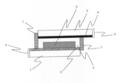
- a counter electrode 9 composed of the support substrate 5 and the counter electrode conductive layer 6 is formed by depositing a platinum film as a counter electrode conductive layer 6 on the support substrate 5 which is a glass substrate provided with a transparent conductive film. Formed.
- the counter electrode 9 and the semiconductor electrode composed of the porous semiconductor layer 3 on which the dye is adsorbed, the transparent conductive film 2 and the support substrate 1 are faced to each other, and a heat compression film spacer for short circuit prevention is interposed therebetween. Together, they are tightly sealed to form a member represented by the leakage preventing agent 7 in the figure.
- electrolytes such as 1,2-dimethyl-3-propylimidazolium iodide (0.6M), lithium iodide (0.1M), iodine (0.05M), and 4-tert- A solar cell was produced by injecting an acetonitrile solution of butylpyridine (0.5 M) to form the carrier transport layer 4.
- the obtained solar cell was irradiated with light having an intensity of 100 mWcm ⁇ 2 (AM1.5, solar simulator), and current-voltage characteristics were measured.
- Table 1A shows the results of the obtained photoelectric conversion characteristics (short-circuit current density (Jsc), open circuit voltage (Voc), form factor (FF), photoelectric conversion efficiency).
- Comparative Example 1 As a sensitizing dye, purified black dye (BD) (purity 99%) is dissolved in ethanol to a concentration of 2 ⁇ 10 ⁇ 4 M and deoxycholic acid to a concentration of 2 ⁇ 10 ⁇ 2 M and adsorbed. A working solution was prepared. A porous semiconductor layer glass plate produced in the same manner as in Example 1 was immersed in the above-mentioned adsorption solution to adsorb the dye, and in the same manner as in Example 1, a solar cell was produced, and the photoelectric conversion characteristics were It was measured. The results are shown in Table 1B.
- BD purified black dye
- An organic dye having a large molecular weight and having an alkyl side chain in the molecule shows a high open-circuit voltage. This is because the alkyl side chain suppresses the association between the dye molecules, and at the same time, the hydrophobic layer formed of the alkyl group as described above suppresses the electrolyte from invading the semiconductor surface. It is thought that there is.
- the present invention since a dye-sensitized solar cell having an unprecedented high photoelectric conversion efficiency can be obtained, the present invention can make a great industrial contribution.
Landscapes
- Chemical & Material Sciences (AREA)
- Organic Chemistry (AREA)
- Engineering & Computer Science (AREA)
- Materials Engineering (AREA)
- Power Engineering (AREA)
- Physics & Mathematics (AREA)
- Spectroscopy & Molecular Physics (AREA)
- Microelectronics & Electronic Packaging (AREA)
- Chemical Kinetics & Catalysis (AREA)
- Hybrid Cells (AREA)
- Photovoltaic Devices (AREA)
Abstract
Description
(a)導電性支持体。
(b)多孔性半導体層。
(c)前記多孔性半導体層に吸着され、分子サイズが異なるとともに、少なくとも一方は分子内に少なくとも一つのアルキル側鎖を有する二種類の増感色素。
(d)キャリア輸送層。
(e)対極。
(a)導電性支持体。
(b)多孔性半導体層。
(c)前記多孔性半導体層に吸着され、分子サイズが異なるとともに、少なくとも一方は単独で示す光電変換特性開放電圧が0.65V以上である二種類の増感色素。
(d)キャリア輸送層。
(e)対極。

また、R1~R5の少なくとも一つが、炭素数が3~16個であるアルキル側鎖部分を有するアルコキシ基、ジアルキルアミノ基、または脂環式アミノ基であってよい。


本発明で用いられる導電性支持体としては、金属のように支持体自体が導電性を有するものでよい。あるいは、表面に導電層を有するガラス、プラスチック等の支持体を利用することもできる。後者の場合、導電層の好ましい導電材料としては、金、白金、銀、銅、アルミニウム、インジウム等の金属、導電性カーボン、またはインジウム-スズ酸化物、酸化スズにフッ素をドープしたもの等があり、これらの導電材料を用いて導電層を支持体上に通常の方法で形成することができる。これらの導電層の膜厚は0.02~5μm程度が好ましい。導電性支持体としては表面抵抗が低い程良く、表面抵抗は40Ω/sq以下であることが好ましい。導電性支持体を受光面とする場合、透明であることが好ましい。また、導電性支持体の膜厚は、光電変換層に適当な強度を付与することができるものであれば特に限定されない。これらの点および機械的な強度を考慮すると、酸化スズにフッ素をドープしたものからなる導電層をソーダ石灰フロートガラスからなる透明性基板上に積層したものを代表的な支持体として使用できる。
多孔性半導体層は半導体微粒子の集合体からなり、半導体微粒子としては、一般に光電変換材料に使用されるものであればどのようなものでも使用できる。例えば、酸化チタン、酸化亜鉛、酸化錫、酸化鉄、酸化ニオブ、酸化ジルコニウム、酸化セリウム、酸化タングステン、酸化シリコン、酸化アルミニウム、酸化ニッケル、チタン酸バリウム、チタン酸ストロンチウム、硫化カドミウム、硫化鉛、硫化亜鉛、リン化インジウム、銅-インジウム硫化物等の単独又は組み合わせが挙げられる。その中でも、酸化チタン、酸化亜鉛、酸化錫、酸化ニオブが好ましく、安定性及び安全性の点から、酸化チタンが特に好ましい。
増感色素を多孔性半導体に吸着させる方法としては、増感色素を溶解した溶液中に半導体電極を浸漬させる方法が一般的である。色素溶液の溶媒としては、アルコール、トルエン、アセトニトリル、テトラヒドロフラン、クロロホルム、ジメチルホルムアミド等の有機溶剤が挙げられ、溶解性を上げるために、二種類以上の溶剤を混合しても良い。溶媒中の色素濃度は、増感色素や溶媒の種類に応じて適宣調整するが、0.01~10mM程度が好ましい。また、必要に応じて、色素分子の会合を低減するためにデオキシコール酸などを添加しても良い。浸漬時間は使用する増感色素、溶媒の種類、溶液の濃度等に応じて適宣調整するが、2~50時間が好ましく、浸漬の際の温度としては10~50℃が好ましい。浸漬は、一回でも良いし、複数回行っても良い。また、色素の吸着量が多い場合、半導体に直接結合していない色素は太陽電池のキャリア輸送層に遊離してきて光電変換効率の低下の原因になるので、色素溶液に浸漬した後、有機溶剤で洗浄して、未吸着の色素を除去するのが好ましい。洗浄剤としては、比較的揮発性の高いメタノール、エタノール、アセトニトリル、アセトン等が挙げられる。また、洗浄により余分な色素を除去した後、色素の吸着状態をより安定にするために半導体の表面を有機塩基性化合物で処理して、未吸着色素の除去を促進しても良い。有機塩基性化合物としては、ピリジン、キノリンなどの誘導体が挙げられる。これらの化合物が液体の場合にはそのまま用いても良いが、固体の場合には色素溶液と同じ溶剤に溶解して用いても良い。
キャリア輸送層は、電子、正孔、イオンを輸送できる導電性材料を含有する。このような導電性材料としては、例えば、ポリビニルカルバゾール、トリフェニルアミン等の正孔輸送材料;テトラニトロフロレノン等の電子輸送材料;ポリチオフェン、ポリピロール等の導電性ポリマー、液体電解質、高分子電解質等のイオン導電体;ヨウ化銅、チオシアン酸銅などの無機P型半導体が挙げられる。
対極は色素増感半導体電極とともに一対の電極を構成し得るものであり、通常、支持基板上に導電層、触媒層が半導体電極側に向かって積層されて形成される。支持基板としては、太陽電池の基盤として使用できる透明または不透明の基盤が挙げられる。導電層の材料としては、N型またはP型の元素半導体(例えば、シリコン、ゲルマニウム等)、化合物半導体(例えば、GaAs、InP、ZnSe、CsS等)、金、白金、銀、銅、アルミニウム等の金属、チタン、タンタル、タングステン等の高融点金属、ITO、SnO2、CuI、ZnO等の透明導電材料が挙げられる。これらの導電層は常法により支持基板上に形成でき、膜厚は0.1~1.0μm程度が適当である。触媒層の材料としては、白金、カーボンブラック、カーボンナノチューブ、フラーレン等が挙げられる。白金の場合、スパッタ、塩化白金酸の熱分解、電着等の方法により、導電層の上に形成できる。また、酸化還元の触媒効果を向上させる目的で、半導体電極に面している側は微細構造で表面積が増大していることが好ましく、例えば、白金であれば白金黒状態に、カーボンであれば多孔質状態になっていることが好ましい。
対極と多孔性半導体層との接触を防止するために、その間にスペーサーを挿入しても良い。スペーサーとしては、ポリエチレン等の高分子フィルムが用いられる。このフィルムの膜厚は10~50μm程度が適当である。
(1) II-1 [2-シアノ-3-(5-(2,4-ジメトキシフェニル)チオフェン-2-イル)アクリル酸]の合成

2,4-ジメトキシフェニルボロン酸(972 mg, 5.34 mmol)、5-ブロモチオフェン-2-カルボキサルデヒド(874 mg, 4.57 mmol)とPd(PPh3)4(135 mg)をトルエンとエタノールの混合溶媒(80 ml / 40 ml)に溶解する。そこに、炭酸カリウム(2 g)の水溶液(15 ml)を加え、反応混液をアルゴン雰囲気下24時間加熱還流する。水を加え、ジクロロメタンで抽出し、抽出液を無水硫酸ナトリウムで乾燥後、減圧下濃縮する。残渣をシリカゲルのカラムクロマトグラフィ一(ジクロロメタン/ヘキサン= 2/1)で精製し、アルデヒド(1)を得た。(1090 mg, 96%)
1H NMR(600 MHz, CDCl3): δ9.88 (s, 1H), 7.70 (d, J= 4.2 Hz, 1H), 7.65 (d, J= 8.4 Hz, 1H), 7.49 (d, J= 4.2 Hz, 1H), 6.58 (dd, J= 8.4 and 2.4 Hz, 1H), 6.55 (d, J= 2.4 Hz, 1H), 3.95 (s, 3H), 3.86 (s, 3H).
アルデヒド(1)(1085 mg, 4.37 mmol)とシアノ酢酸(372 mg, 4.37 mmol)をアセトニトリル(50 ml)に溶解し、ピペリジン(0.35 ml)を加え、アルゴン雰囲気下24時間加熱還流する。反応混液を2N HClで酸性にし、水を加え、ジクロロメタンで抽出し、抽出液を無水硫酸ナトリウムで乾燥後、減圧下濃縮する。残渣をシリカゲルのカラムクロマトグラフィ一(ジクロロメタン→メタノール)で精製し、II-1を赤色固体で得た。(161 mg, 11%)
1H NMR (600 MHz, DMSO-d6):δ8.44 (s, 1H), 7.96 (d, J= 4.2 Hz, 1H), 7.86 (d, J= 8.4 Hz, 1H), 7.75 (d, J= 4.2 Hz, 1H), 6.76 (d, J= 2.4 Hz, 1H), 6.70 (dd, J= 8.4 and 2.4 Hz, 1H), 3.97 (s, 3H), 3.86 (s, 3H).
Exact mass calculated for C16H12NO4S [M-1]-314.0493, observed 314.0498.
UV/VIS (EtOH): λmax = 393 nm (ε 28,400)
合成例1 (1) 増感色素II-1の合成例の、2,4-ジメトキシフェニルボロン酸の代りに4-メトキシフェニルボロン酸を用いて、同様の合成法により、増感色素II-2を合成した。

UV/VIS (EtOH): λmax = 382 nm (ε 32,700)
合成例1 (1) 増感色素II-1の合成例の、2,4-ジメトキシフェニルボロン酸の代りにフェニルボロン酸を用いて、同様の合成法により、増感色素II-3を合成した。

UV/VIS (EtOH): λmax = 365 nm (ε 31,500)
合成例1 (1) 増感色素II-1の合成例の、2,4-ジメトキシフェニルボロン酸の代りに4-ジメチルアミノフェニルボロン酸を用いて、同様の合成法により、増感色素II-4を合成した。

UV/VIS (EtOH): λmax = 424 nm (ε 27,600)
(1) II-5 [2-シアノ-3-(5-(4-オクチルオキシフェニル)チオフェン-2-イル)アクリル酸]の合成

4-ブロモフェノール(1.0 g, 5.78 mmol)、1-ヨードオクタン(1.67 g, 6.94 mmol)と炭酸カリウム(4.0 g, 29 mmol) をDMF(40 ml) に溶解し、24時間加熱還流する。反応混液に水を加えて、ジクロロメタンで抽出し、抽出液を無水硫酸ナトリウムで乾燥後、減圧下濃縮する。残渣をシリカゲルのカラムクロマトグラフィ一(ジクロロメタン/ヘキサン=1/1)で精製し、ブロミド(2)(1.48 g)を得た。
1H NMR (600 MHz, CDCl3):δ9.86 (s, 1H), 7.71 (d, J= 3.6 Hz, 1H), 7.60 (d, J= 9.0 Hz, 2H), 7.29 (d, J= 3.6 Hz, 1H), 6.94 (d, J= 9.0 Hz, 2H), 4.00 (t, J= 6.6 Hz, 2H), 1.80 (m, 2H), 1.46 (m, 2H), 1.38-1.25 (m, 8H), 0.89 (t, J= 6.6 Hz, 3H).
アルデヒド(3)(140 mg, 0.44 mmol)とシアノ酢酸(40 mg, 0.47 mmol)をアセトニトリル(30 ml)に溶解し、ピペリジン(0.1 ml)を加え、アルゴン雰囲気下、24時間加熱還流する。反応混液を2N HClで酸性化し、水を加えて、ジクロロメタンで抽出する。抽出液を無水硫酸ナトリウムで乾燥後、減圧下濃縮する。残渣をシリカゲルのカラムクロマトグラフィ一(ジクロロメタン→メタノール)で精製し、II-5を橙色固体として得た。(115 mg, 68%)
1H NMR (600 MHz, DMSO-d6):δ8.47 (s, 1H), 7.99 (d, J= 3.6 Hz, 1H), 7.73 (d, J= 9.0 Hz, 2H), 7.66 (d, J= 3.6 Hz, 1H), 7.04 (d, J= 9.0 Hz, 2H), 4.03 (t, J= 6.6 Hz, 2H), 1.73 (m, 2H), 1.42 (m, 2H), 1.35-1.29 (m, 8H), 0.86 (t, J= 6.6 Hz, 3H).
Exact mass calculated for C22H24NO3S [M-1]-382.1482, observed 382.1488.
UV/VIS (EtOH): λmax = 384 nm (ε 30,100)
4-ブロモレソルシノールと1-ヨードブタンから、1-ブロモ-2,4-ジブトキシベンゼンを調製し、合成例2 (1) 増感色素II-5の合成例と同様の合成法により増感色素II-6を合成した。

UV/VIS (EtOH): λmax = 396 nm (ε 30,200)
4-ブロモレソルシノールと1-ヨードオクタンから、1-ブロモ-2,4-ジオクチルオキシベンゼンを調製し、合成例2 (1) 増感色素II-5の合成例と同様の合成法により増感色素II-7を合成した。

Exact mass calculated for C30H40NO4S [M-1]- 510.2684, observed 510.2690.
UV/VIS (EtOH): λmax = 395 nm (ε26,100)
4-ブロモレソルシノールと1-ヨードヘキサデカンから、1-ブロモ-2,4-ビス(ヘキサデシルオキシ)ベンゼンを調製し、合成例2 (1) 増感色素II-5の合成例と同様の合成法により増感色素II-8を合成した。

Exact mass calculated for C46H72NO4S [M-1]-734.5188, observed 734.5198.
UV/VIS (EtOH): λmax = 392 nm (ε 26,900)
1-ブロモ-4-ブトキシベンゼンから、合成例2 (1) 増感色素II-5の合成例と同様の合成法により増感色素II-9を合成した。

Exact mass calculated for C18H16NO3S [M-1]- 326.0856, observed 326.0859.
UV/VIS (DMSO): λmax = 377 nm (ε 25,600)
(1) II-10 [2-シアノ-3-(5-(4-ジブチルアミノフェニル)チオフェン-2-イル)アクリル酸]の合成

N,N-ジブチルアニリン(5.0 g, 24.3 mmol)のDMF(50 ml)溶液にNBS(4.3 g, 24.3 mmol) を加え、室温で1.5時間撹拌する。反応溶液に水を加え、反応生成物をジクロロメタンで抽出する。抽出液を無水硫酸ナトリウムで乾燥後、減圧下濃縮する。残渣をシリカゲルのカラムクロマトグラフィ一(ヘキサン)で精製し、油状物質のブロミド(4)(6.17 g)を得た。
1H NMR (600 MHz, CDCl3):δ9.81 (s, 1H), 7.77 (d, J = 4.2 Hz, 1H), 7.53 (d, J = 9.0 Hz, 2H), 7.21 (d, J = 4.2 Hz, 1H), 6.64 (d, J = 9.0 Hz, 2H), 3.31 (t, J = 7.2 Hz, 4H), 1.57 (m, 4H), 1.38 (m, 4H), 0.97 (t, J = 7.2 Hz, 6H).
アルデヒド(5)(424 mg, 1.34 mmol)とシアノ酢酸(114 mg, 1.34 mmol)をアセトニトリル(30 ml)に溶解し、ピペリジン(0.1 ml)を加えて、アルゴン雰囲気下、24時間加熱還流する。反応混液を2N HClで酸性化し、水を加えて、ジクロロメタンで抽出し、抽出液を無水硫酸ナトリウムで乾燥後、減圧下濃縮する。残渣をシリカゲルのカラムクロマトグラフィ一(ジクロロメタン→メタノール)で精製し、II-10を暗赤色固体で得た。(148 mg, 29%)
1H NMR (600 MHz, DMSO-d6):δ8.39 (s, 1H), 7.92 (d, J= 4.2 Hz, 1H), 7.58 (d, J= 9.0 Hz, 2H), 7.51 (d, J= 4.2 Hz, 1H), 6.71 (d, J= 9.0 Hz, 2H), 3.34 (t, J= 7.2 Hz, 4H), 1.52 (m, 4H), 1.33 (m, 4H), 0.92 (t, J= 7.2 Hz, 6H).
Exact mass calculated for C22H25N2O2S [M-1]- 381.1642, observed 381.1649.
UV/VIS (EtOH): λmax = 438 nm (ε20,500)
アニリンと1-ヨードオクタンから、N,N-ジオクチルアニリンを調製し、合成例3 (1) 増感色素II-10の合成例と同様の合成法により増感色素II-11を合成した。

Exact mass calculated for C30H41N2O2S [M-1]- 493.2894, observed 493.2901.
UV/VIS (EtOH): λmax = 438 nm (ε31,600)
(1) II-12 [2-シアノ-3-(5-(4-ジブチルアミノフェニル)-4-オクチルチオフェン-2-イル)アクリル酸]の合成

ブロミド(4)(1000 mg, 3.52 mmol)をアルゴン雰囲気下、無水THF(100 ml)に溶解し、-78℃に冷却してから、n-ブチルリチウムの15% ヘキサン溶液(2.6 ml, 4.22 mmol) を滴下し、滴下終了後、-78℃で更に2時間撹拌する。2-イソプロポキシ-4,4,5,5-テトラメチル-1,3,2-ジオキサボロラン(851 mg, 4.58 mmol)を滴下し、24時間撹拌を続けながら反応温度を室温に戻す。反応混液に水を加え、酢酸エチルで抽出し、抽出液を硫酸ナトリウムで乾燥後、減圧下濃縮し、ボロン酸(6)(1095 mg , 3.3 mmol)を得た。このボロン酸(6)、2-ブロモ-3-オクチルチオフェン(1092 mg, 3.97 mmol)、及びPd(PPh3)4(114 mg)をトルエン(100 ml)に溶解し、炭酸カリウム(5 g)の水溶液(20 ml)を加え、アルゴン雰囲気下、24時間加熱還流する。反応混液に水を加え、ジクロロメタンで抽出し、抽出液を無水硫酸ナトリウムで乾燥後、減圧下濃縮する。残渣をシリカゲルのカラムクロマトグラフィ一(ジクロロメタン/ヘキサン=1/2)で精製し、チオフェン(7)(900mg, 2.25 mmol)を得た。このチオフェン(7)をDMFに溶解させ、0℃に冷却し、オキシ塩化リン(863 mg, 5.63 mmol)を滴下し、アルゴン雰囲気下、70℃で4時間撹拌する。反応混液を2N NaOHで中和し、ジクロロメタンで抽出し、抽出液を無水硫酸ナトリウムで乾燥後、減圧下濃縮する。残渣をシリカゲルのカラムクロマトグラフィ一(ジクロロメタン/ヘキサン=1/1)で精製し、アルデヒド(8)を得た。(720 mg , 43%)
1H NMR (600 MHz, An-d6):δ9.85 (s, 1H), 7.84 (s, 1H), 7.35 (d, J= 8.4 Hz, 2H), 6.78 (d, J= 8.4 Hz, 2H), 3.40 (t, J= 7.8 Hz, 4H), 2.74 (t, J= 7.8 Hz, 2H), 1.67 (m, 2H), 1.62 (m, 4H), 1.44~1.22 (m, 14H), 0.97 (t, J= 7.2 Hz, 6H), 0.87 (t, J= 7.2 Hz, 3H).
アルデヒド(8)(720 mg, 1.68 mmol) とシアノ酢酸(143 mg, 1.68 mmol)をアセトニトリル(30 ml)に溶解し、ピペリジン(0.1 ml)を加え、アルゴン雰囲気下、24時間加熱還流する。反応溶液に2N HClを加えてから、水を加え、ジクロロメタンで抽出し、抽出液を無水硫酸ナトリウムで乾燥後、減圧下濃縮する。残渣をシリカゲルのカラムクロマトグラフィー(ジクロロメタン→メタノール)で精製し、赤褐色固体のII-12を得た。 (580 mg, 70%)
1H NMR (600 MHz, CDCl3):δ8.24 (s, 1H), 7.63 (s, 1H), 7.35 (d, J= 7.8 Hz, 2H), 6.65 (d, J= 7.8 Hz, 2H), 3.31 (t,, J= 7.2 Hz, 4H), 2.69 (m, 2H), 1.60 (m, 6H), 1.38 (m, 4H), 1.26 (m, 10H), 0.98 (t, J= 7.2 Hz, 6H), 0.87 (t, J= 7.2 Hz, 3H). Exact mass calculated for C30H41N2O2S [M-1]-493.2894, observed 493.2904. UV/VIS (EtOH): λmax = 280, 412 nm (ε 16,000, 18,500)
1-ブロモ-2,4-ジブトキシベンゼンと2-ブロモチアゾールから、合成例4 (1) 増感色素II-12の合成例と同様の合成法により、増感色素II-13を合成した。

Exact mass calculated for C21H23N2O4S [M-1]- 399.1384, observed 399.1389.
UV/VIS (EtOH): λmax = 386 nm (ε18,200)
1-ブロモ-2,4-ジブトキシベンゼンから、合成例4 (1) 増感色素II-12の合成例と同様の合成法により、増感色素II-14を合成した。

Exact mass calculated for C30H40NO4S [M-1]- 510.2684, observed 510.2687.
UV/VIS (EtOH): λmax = 360 nm (ε23,200)

塩化亜鉛(136 mg, 1.12 mmol)を無水THF(20 ml)に溶解した溶液をアルゴン雰囲気下、室温で撹拌し、その溶液中に2-チエニルマグネシウムブロミドの1.0M THF溶液(419 mg, 2.24 mmol)を滴下する。滴下終了後、室温で更に30分間撹拌してジチオフェン-2-イル亜鉛溶液を調製する。 その溶液中に、2-ブロモ-1,3,5-トリメトキシベンゼン(394 mg, 1.59 mmol)、1-メチル-2-ピロリドン(3 ml)とPdCl2(dppf)(39 mg)を無水ジオキサン(20 ml)に溶解した溶液を滴下する。反応混液をアルゴン雰囲気下、24時間加熱還流する。反応混液に1N HClを加えてから、水を加え、ジクロロメタンで抽出し、抽出液を無水硫酸ナトリウムで乾燥後、減圧下濃縮する。残渣をシリカゲルのカラムクロマトグラフィ一(ジクロロメタン/ヘキサン= 1/1)で精製し、カップリング生成物(9)を得た。(132 mg, 47%)
1H NMR (600 MHz, CDCl3): δ 7.33 (dd, J= 5.4 and 1.2 Hz, 1H), 7.30 (dd, J= 3.6 and 1.2 Hz, 1H), 7.07 (dd, J= 5.4 Hz, 3.6Hz, 1H), 6.22 (s, 2H), 3.85 (s, 3H), 3.81 (s, 6H).
カップリング生成物(9)(132 mg , 0.53 mmol)のDMF(10 ml)溶液を0℃に冷却し、オキシ塩化リン(201 mg, 1.31 mmol)をゆっくりと加える。反応混液をアルゴン雰囲気下、70℃に2時間加熱する。反応混液を1N NaOHで中和し、水を加えて、ジクロロメタンで抽出し、抽出液を無水硫酸ナトリウムで乾燥後、減圧下濃縮して、アルデヒド(10)(140 mg)を得た。このアルデヒドとシアノ酢酸(42 mg, 0.50 mmol) をアセトニトリル(30 ml) に溶解し、ピペリジン(0.1 ml)を加え、アルゴン雰囲気下、24時間加熱還流する。反応混液を2N HCl で酸性化してから、水を加え、ジクロロメタンで抽出し、抽出液を無水硫酸ナトリウムで乾燥後、減圧下濃縮する。残渣をシリカゲルのカラムクロマトグラフィ一(ジクロロメタン→メタノール)で精製し、II-15を赤色固体として得た。(123 mg, 67%)
1H NMR (600 MHz, DMSO-d6): δ 8.40 (s, 1H), 7.91 (d, J= 4.2 Hz, 1H), 7.65 (d, J= 4.2 Hz, 1H), 6.40 (s, 2H), 3.86 (s, 9H).
Exact mass calculated for C17H14NO5SNa [M+Na]+ 368.0569 , observed 368.0559 .
UV/VIS (EtOH): λmax = 389 nm (ε18,700)

4-ブロモレソルシノール(2.0 g , 10.6 mmol)、1-ヨードブタン(5.1 g, 27.5 mmol)、炭酸カリウム(16 g, 58 mmol)をDMF(80 ml)に溶解し、アルゴン雰囲気下、24時間加熱還流する。反応混液に水を加え、ジクロロメタンで抽出し、抽出液を硫酸ナトリウムで乾燥後、減圧下濃縮する。残渣をシリカゲルのカラムクロマトグラフィ一(ヘキサン/ジクロロメタン= 2 / 1)で精製し、油状物質のブロミド(11)(3.0 g)を得た。
1H NMR (600 MHz, CDCl3): δ 9.88 (s, 1H), 7.70 (d, J= 4.2 Hz, 1H), 7.63 (d, J= 7.8 Hz, 1H), 7.49 (d, J= 4.2 Hz, 1H), 6.55 (d, J= 7.8 Hz, 1H), 6.55 (s, 1H), 4.11 (t, J= 6.6 Hz, 2H), 4.01 (t, J= 6.6 Hz, 2H), 1.92 (m, 2H), 1.79 (m, 2H), 1.56 (m, 2H), 1.52 (m, 2H), 1.00 (t, J= 7.8 Hz, 3H), 0.99 (t, J= 7.8 Hz, 3H).
アルデヒド(12)(310 mg, 0.93 mmol)とロダニン-3-酢酸(178 mg, 0.93 mmol)をアセトニトリル(30 ml)に溶解し、ピペリジン(0.1 ml)を加え、アルゴン雰囲気下で24時間加熱還流する。反応混液を2N HClで酸性化してから、水を加え、ジクロロメタンで抽出し、抽出液を硫酸ナトリウムで乾燥後、減圧下濃縮する。残渣をシリカゲルのカラムクロマトグラフィ一(ジクロロメタン→メタノール)で精製し、赤色固体のII-16を得た。(370 mg, 78%)
1H NMR (600 MHz, DMSO-d6):δ8.14 (s, 1H), 7.90 (d, J= 9.0 Hz, 1H), 7.80 (d, J= 4.2 Hz, 1H), 7.77 (d, J= 4.2 Hz, 1H), 6.72 (d, J= 2.4 Hz, 1H), 6.65 (dd, J= 9.0 and 2.4 Hz, 1H), 4.69 (s, 1H), 4.21 (t, J= 6.0 Hz, 2H), 4.05 (t, J= 6.6 Hz, 2H), 1.95 (m, 2H), 1.73-1.68 (m, 4H), 1.45 (q, J= 7.2 Hz, 2H), 1.07 (t, J= 7.2 Hz, 3H), 0.95 (t, J= 7.2 Hz, 3H).
Exact mass calculated for C24H26NO5S3[M-1]- 504.0979, observed 504.0985.
UV/VIS (EtOH): λmax = 467 nm (ε 41,200)
なお、一般式(1)ではアクセプター部位をシアノアクリル酸に固定しているが、色素II-16では、上掲の化学構造式からわかるように、アクセプター部位がロダニン-酢酸である。このように、一般式(1)のシアノアクリル酸をロダニン-酢酸で置き換えても、後述する表1に示すように他の色素との組み合わせにより高い変換効率を発揮する。
・多孔性半導体層の作製
日本板硝子社製のSnO2膜付きガラスの透明導電側に、市販の酸化チタンペースト(Solaronix社製、Ti nanoxide T/SP)をスクリーン印刷により、20μm程度の膜厚、5mm×5mm程度の面積で、透明導電膜の上に塗布した。更に、CCIC社製PST 400をその上に塗布する(5μm)。得られた塗膜を、100℃で30分間予備乾燥した後、大気雰囲気中で500℃で2時間焼成することで、多孔性半導体層として膜厚25μmの酸化チタン膜を得た。
増感色素Iとして、精製したブラックダイ(BD)(純度99%)を濃度2×10⁻⁴M、また、増感色素IIとして、増感色素II-1を濃度2×10⁻⁴Mとなるようにエタノールに溶解した。この溶液に、デオキシコール酸を濃度2×10⁻²Mとなるように加えて溶解させ、増感色素IとIIの混合吸着用溶液を調製した。この溶液に上記ガラス板を24時間浸漬させることにより、多孔性半導体層に色素を吸着させた。
図1にその構造を模式的に示す太陽電池を作成した。具体的には、先ず透明導電膜を備えたガラス基板である支持基板5上に対極導電層6として、白金膜を1μm蒸着することにより、支持基板5及び対極導電層6から構成される対極9を形成した。この対極9と上記の色素を吸着させた多孔性半導体層3、透明導電成膜2及び支持基板1からなる半導体電極とを向かい合わせ、間に短絡防止のための熱圧縮フィルムスペーサーを挟んで重ね合わせて密着封装して、図中の漏洩防止剤7で表される部材を形成する。その後、両極の隙間に電解液であるヨウ化1,2-ジメチル-3-プロピルイミダゾリウム(0.6M)、ヨウ化リチウム(0.1M)、ヨウ素(0.05M)、及び4-tert-ブチルピリジン(0.5M)のアセトニトリル溶液を注入してキャリア輸送層4を形成することで、太陽電池を作製した。
増感色素IIに増感色素II-2~16、式(6)、式(7)、式(8)、式(10)、式(12)、式(14)、式(15)の化合物を用いて、実施例1と同様にして、太陽電池を作製し、光電変換特性を測定した。結果を表1Aに示す。
増感色素として、精製したブラックダイ(BD)(純度99%)を濃度2×10⁻⁴M、また、デオキシコール酸を濃度2×10⁻²Mとなるようにエタノールに溶解して、吸着用溶液を調製した。実施例1と同様にして作製した多孔性半導体層のガラス板を、上記の吸着溶液に浸漬して、色素を吸着させ、実施例1と同様にして、太陽電池を作製し、光電変換特性を測定した。結果を表1Bに示す。
増感色素として増感色素II-1~16、式(6)、式(7)、式(8)、式(10)、式(12)、式(14)、式(15)の化合物を用いて、比較例1と同様にして、太陽電池を作製し、光電変換特性を測定した。結果を表1Bに示す。


2 透明導電性膜
3 多孔性半導体層
4 キャリア輸送層
5 支持基板
6 対極導電層
7 漏洩防止剤
8 透明導電性支持体
9 対極
Claims (16)
- 以下の(a)~(e)を設けた、色素増感太陽電池。
(a)導電性支持体。
(b)多孔性半導体層。
(c)前記多孔性半導体層に吸着され、分子サイズが異なるとともに、少なくとも一方は分子内に少なくとも一つのアルキル側鎖を有する二種類の増感色素。
(d)キャリア輸送層。
(e)対極。 - 前記二種類の増感色素のうちの少なくとも一方は単独で示す光電変換特性開放電圧が0.65V以上である、請求項1に記載の色素増感太陽電池。
- 以下の(a)~(e)を設けた、色素増感太陽電池。
(a)導電性支持体。
(b)多孔性半導体層。
(c)前記多孔性半導体層に吸着され、分子サイズが異なるとともに、少なくとも一方は単独で示す光電変換特性開放電圧が0.65V以上である二種類の増感色素。
(d)キャリア輸送層。
(e)対極。 - 前記二種類の増感色素の少なくとも一方は分子内に少なくとも一つのアルキル側鎖を有する、請求項3に記載の色素増感太陽電池。
- 前記二種類の増感色素の分子サイズの小さい方の増感色素は以下の式(1)によって表わされる有機色素である、請求項1から4の何れかに記載の色素増感型太陽電池。

- R1~R5の少なくとも一つが、炭素数が3~16個であるアルキル側鎖部分を有するアルコキシ基、ジアルキルアミノ基、または脂環式アミノ基である、請求項5に記載の色素増感型太陽電池。
- 前記アルキル側鎖部分はメチル基、エチル基、プロピル基、ブチル基、ペンチル基、ヘキシル基、ヘプチル基、オクチル基、ヘキサデシル基、イソプロピル基、イソブチル基、イソペンチル基、イソヘキシル基、イソへプチル基、イソオクチル基、ネオペンチル基、ネオヘキシル基、ネオへプチル基、ネオオクチル基、sec-ブチル基、sec-ペンチル基、sec-ヘキシル基、sec-ヘプチル基、sec-オクチル基、tert-ブチル基、tert-ペンチル基、tert-ヘキシル基、tert-ヘプチル基、tert-オクチル基、2-エチルヘキシル基、および1,1,3,3-テトラメチルブチル基からなる群から選択される、請求項6に記載の色素増感型太陽電池。
- 前記脂環式アミノ基はピロリジンまたはピペリジンである、請求項6または7に記載の色素増感型太陽電池。
- 前記芳香族複素環基は下式(2)中の何れかの構造を有する、請求項5から8の何れかに記載の色素増感型太陽電池。

- 前記二種類の増感色素のうちの一方はルテニウムピリジン錯体である、請求項1から9の何れかに記載の色素増感太陽電池。
- 前記二種類の増感色素のうちの一方はターピリジン系ルテニウム錯体である、請求項1から9の何れかに記載の色素増感太陽電池。
- 以下の式によって表わされる増感色素。

- R1~R5の少なくとも一つが、炭素数が3~16個であるアルキル側鎖部分を有するアルコキシ基、ジアルキルアミノ基、または脂環式アミノ基である、請求項12に記載の増感色素。
- 前記アルキル側鎖部分はメチル基、エチル基、プロピル基、ブチル基、ペンチル基、ヘキシル基、ヘプチル基、オクチル基、ヘキサデシル基、イソプロピル基、イソブチル基、イソペンチル基、イソヘキシル基、イソへプチル基、イソオクチル基、ネオペンチル基、ネオヘキシル基、ネオへプチル基、ネオオクチル基、sec-ブチル基、sec-ペンチル基、sec-ヘキシル基、sec-ヘプチル基、sec-オクチル基、tert-ブチル基、tert-ペンチル基、tert-ヘキシル基、tert-ヘプチル基、tert-オクチル基、2-エチルヘキシル基、および1,1,3,3-テトラメチルブチル基からなる群から選択される、請求項13に記載の増感色素。
- 前記脂環式アミノ基はピロリジンまたはピペリジンである、請求項13または14に記載の増感色素。
- 前記芳香族複素環基は下式(4)中の何れかの構造を有する、請求項12から15の何れかに記載の増感色素。

Priority Applications (3)
| Application Number | Priority Date | Filing Date | Title |
|---|---|---|---|
| JP2013530076A JP5794589B2 (ja) | 2011-08-25 | 2012-08-24 | 色素増感太陽電池及び増感色素 |
| US14/240,498 US20140202537A1 (en) | 2011-08-25 | 2012-08-24 | Dye-sensitized solar cell and sensitizing dye |
| EP12825038.8A EP2752935A4 (en) | 2011-08-25 | 2012-08-24 | SOLAR CELL SENSITIZED BY A COLORING AND COLORING SENSITIZER |
Applications Claiming Priority (2)
| Application Number | Priority Date | Filing Date | Title |
|---|---|---|---|
| JP2011-183404 | 2011-08-25 | ||
| JP2011183404 | 2011-08-25 |
Publications (1)
| Publication Number | Publication Date |
|---|---|
| WO2013027838A1 true WO2013027838A1 (ja) | 2013-02-28 |
Family
ID=47746573
Family Applications (1)
| Application Number | Title | Priority Date | Filing Date |
|---|---|---|---|
| PCT/JP2012/071505 Ceased WO2013027838A1 (ja) | 2011-08-25 | 2012-08-24 | 色素増感太陽電池及び増感色素 |
Country Status (4)
| Country | Link |
|---|---|
| US (1) | US20140202537A1 (ja) |
| EP (1) | EP2752935A4 (ja) |
| JP (1) | JP5794589B2 (ja) |
| WO (1) | WO2013027838A1 (ja) |
Cited By (2)
| Publication number | Priority date | Publication date | Assignee | Title |
|---|---|---|---|---|
| CN104073017A (zh) * | 2013-03-28 | 2014-10-01 | 凯惠科技发展(上海)有限公司 | 有机染料敏化剂、制备方法及在光电转换中的应用 |
| WO2015016201A1 (ja) * | 2013-07-31 | 2015-02-05 | 富士フイルム株式会社 | 光電変換素子、光電変換素子の製造方法および太陽電池 |
Families Citing this family (3)
| Publication number | Priority date | Publication date | Assignee | Title |
|---|---|---|---|---|
| KR102087859B1 (ko) * | 2018-07-17 | 2020-03-12 | 한국화학연구원 | 신규 캐소드 버퍼층 소재, 및 이를 포함하는 유기 또는 유/무기 하이브리드 광전소자 |
| CN112209951B (zh) * | 2019-07-12 | 2023-05-09 | 湘潭大学 | 一种苯并咪唑衍生物与8-羟基喹啉衍生物合镉配合物染料敏化剂及其制备方法与用途 |
| CN117924237A (zh) * | 2023-12-26 | 2024-04-26 | 湘潭大学 | 一种((2,3-二氨基-5,6-二氟-1,4-苯基)双(噻吩-5,2-二基))双(2-氰基丙烯酸)及其制备方法与用途 |
Citations (7)
| Publication number | Priority date | Publication date | Assignee | Title |
|---|---|---|---|---|
| JP2000268892A (ja) | 1999-01-14 | 2000-09-29 | Fuji Photo Film Co Ltd | 光電変換素子および光電池 |
| JP2003249279A (ja) | 2002-02-26 | 2003-09-05 | Sharp Corp | 多孔質半導体層の作製方法及び色素増感型太陽電池 |
| WO2004082061A1 (ja) * | 2003-03-14 | 2004-09-23 | Nippon Kayaku Kabushiki Kaisha | 色素増感光電変換素子 |
| JP2006107885A (ja) | 2004-10-04 | 2006-04-20 | Sharp Corp | 色素増感太陽電池および色素増感太陽電池モジュール |
| JP2006278112A (ja) | 2005-03-29 | 2006-10-12 | Sharp Corp | 色素増感太陽電池及び色素増感太陽電池モジュール |
| JP2009032547A (ja) * | 2007-07-27 | 2009-02-12 | Sony Corp | 色素増感光電変換素子およびその製造方法ならびに電子機器ならびに半導体電極およびその製造方法 |
| JP2009212035A (ja) | 2008-03-06 | 2009-09-17 | Konica Minolta Business Technologies Inc | 色素増感光電変換素子及び太陽電池 |
Family Cites Families (2)
| Publication number | Priority date | Publication date | Assignee | Title |
|---|---|---|---|---|
| RU2490746C2 (ru) * | 2007-10-25 | 2013-08-20 | Сони Корпорейшн | Краситель, содержащий закрепляющую группу в молекулярной структуре |
| TWI382062B (zh) * | 2009-04-29 | 2013-01-11 | Academia Sinica | 有機染料及使用此有機染料的染料敏化太陽能電池 |
-
2012
- 2012-08-24 JP JP2013530076A patent/JP5794589B2/ja not_active Expired - Fee Related
- 2012-08-24 WO PCT/JP2012/071505 patent/WO2013027838A1/ja not_active Ceased
- 2012-08-24 US US14/240,498 patent/US20140202537A1/en not_active Abandoned
- 2012-08-24 EP EP12825038.8A patent/EP2752935A4/en not_active Withdrawn
Patent Citations (7)
| Publication number | Priority date | Publication date | Assignee | Title |
|---|---|---|---|---|
| JP2000268892A (ja) | 1999-01-14 | 2000-09-29 | Fuji Photo Film Co Ltd | 光電変換素子および光電池 |
| JP2003249279A (ja) | 2002-02-26 | 2003-09-05 | Sharp Corp | 多孔質半導体層の作製方法及び色素増感型太陽電池 |
| WO2004082061A1 (ja) * | 2003-03-14 | 2004-09-23 | Nippon Kayaku Kabushiki Kaisha | 色素増感光電変換素子 |
| JP2006107885A (ja) | 2004-10-04 | 2006-04-20 | Sharp Corp | 色素増感太陽電池および色素増感太陽電池モジュール |
| JP2006278112A (ja) | 2005-03-29 | 2006-10-12 | Sharp Corp | 色素増感太陽電池及び色素増感太陽電池モジュール |
| JP2009032547A (ja) * | 2007-07-27 | 2009-02-12 | Sony Corp | 色素増感光電変換素子およびその製造方法ならびに電子機器ならびに半導体電極およびその製造方法 |
| JP2009212035A (ja) | 2008-03-06 | 2009-09-17 | Konica Minolta Business Technologies Inc | 色素増感光電変換素子及び太陽電池 |
Non-Patent Citations (17)
| Title |
|---|
| B. O'REGAN; M. GRAETZEL, NATURE, vol. 353, 1991, pages 737 - 740 |
| C. KIM ET AL., J. ORG. CHEM., vol. 73, 2008, pages 7072 - 7079 |
| C. LI ET AL., CHEMSUSCHEM, vol. 1, 2008, pages 615 - 618 |
| D. P. HAGBERG ET AL., J. AM. CHEM. SOC., vol. 130, 2008, pages 6259 - 6266 |
| HUAJIE CHEN ET AL.: "High Molar Extinction Coefficient Branchlike Organic Dyes Containing Di(p-tolyl)phenylamine Donor for Dye-Sensitized Solar Cells Applications", J. PHYS. CHEM. C, vol. 114, no. 7, 2010, pages 3280 - 3286, XP055143242 * |
| K. R. JUSTIN THOMAS ET AL., CHEM. MATER., vol. 20, 2008, pages 1830 - 1840 |
| M. GRATZEL ET AL., CHEM. EUR. J., vol. 16, 2010, pages 1193 - 1201 |
| NAM-GYU PARK ET AL., SYNTHETIC METALS., vol. 159, 2009, pages 2571 - 77 |
| R. Y. OGURA ET AL., APPL. PHYS. LETT., vol. 94, 2009, pages 073308 |
| S. ITO ET AL., ADV. MATER., vol. 18, 2006, pages 1202 - 1205 |
| S. KIM ET AL., TETRAHEDRON, vol. 63, 2007, pages 11436 - 11443 |
| SE WOONG PARK ET AL.: "Effect of donor moiety in organic sensitizer on spectral response, electrochemical and photovoltaic properties", SYNTHETIC METALS, vol. 159, no. 23-24, 2009, pages 2571 - 2577, XP026806581 * |
| See also references of EP2752935A4 |
| T. DENTANI, NEW J. CHEM., vol. 33, 2009, pages 93 - 101 |
| T. HORIUCHI ET AL., J. AM. CHEM. SOC., vol. 126, 2004, pages 12218 - 12219 |
| W. H. LIU ET AL., CHEM. COMMUN., 2008, pages 5152 - 5154 |
| Z-S. WANG ET AL., CHEM. MATER., vol. 20, 2008, pages 3993 - 4003 |
Cited By (4)
| Publication number | Priority date | Publication date | Assignee | Title |
|---|---|---|---|---|
| CN104073017A (zh) * | 2013-03-28 | 2014-10-01 | 凯惠科技发展(上海)有限公司 | 有机染料敏化剂、制备方法及在光电转换中的应用 |
| WO2014154028A1 (zh) * | 2013-03-28 | 2014-10-02 | 凯惠科技发展(上海)有限公司 | 有机染料敏化剂、制备方法及在光电转换中的应用 |
| WO2015016201A1 (ja) * | 2013-07-31 | 2015-02-05 | 富士フイルム株式会社 | 光電変換素子、光電変換素子の製造方法および太陽電池 |
| JP2015046585A (ja) * | 2013-07-31 | 2015-03-12 | 富士フイルム株式会社 | 光電変換素子、光電変換素子の製造方法および太陽電池 |
Also Published As
| Publication number | Publication date |
|---|---|
| EP2752935A1 (en) | 2014-07-09 |
| JPWO2013027838A1 (ja) | 2015-03-23 |
| JP5794589B2 (ja) | 2015-10-14 |
| EP2752935A4 (en) | 2015-10-28 |
| US20140202537A1 (en) | 2014-07-24 |
Similar Documents
| Publication | Publication Date | Title |
|---|---|---|
| Tang et al. | New starburst sensitizer with carbazole antennas for efficient and stable dye-sensitized solar cells | |
| Chen et al. | Dipolar compounds containing fluorene and a heteroaromatic ring as the conjugating bridge for high‐performance dye‐sensitized solar cells | |
| Lin et al. | Organic dyes containing coplanar diphenyl-substituted dithienosilole core for efficient dye-sensitized solar cells | |
| Yang et al. | Efficient and stable organic DSSC sensitizers bearing quinacridone and furan moieties as a planar π-spacer | |
| Cui et al. | Incorporating benzotriazole moiety to construct D–A− π–A organic sensitizers for solar cells: significant enhancement of open-circuit photovoltage with long alkyl group | |
| Wu et al. | Efficient and stable dye-sensitized solar cells based on phenothiazine sensitizers with thiophene units | |
| Gupta et al. | Carbazole based A-π-D-π-A dyes with double electron acceptor for dye-sensitized solar cell | |
| JP4841248B2 (ja) | 色素増感光電変換素子 | |
| Li et al. | New indole-based metal-free organic dyes for dye-sensitized solar cells | |
| Hong et al. | Performance of dye-sensitized solar cells based on novel sensitizers bearing asymmetric double D− π− A chains with arylamines as donors | |
| Huang et al. | Organic dyes containing a cyanovinyl entity in the spacer for solar cells applications | |
| JP6278504B2 (ja) | 新規化合物及びそれを用いた光電変換素子 | |
| Mao et al. | 2, 6-Conjugated Bodipy sensitizers for high-performance dye-sensitized solar cells | |
| Narayanaswamy et al. | Simple metal-free dyes derived from triphenylamine for DSSC: A comparative study of two different anchoring group | |
| Jia et al. | Synthesis of dendritic triphenylamine derivatives for dye-sensitized solar cells | |
| Wang et al. | Effects of the acceptors in triphenylamine-based D–A′–π–A dyes on photophysical, electrochemical, and photovoltaic properties | |
| Zhang et al. | Anti-recombination organic dyes containing dendritic triphenylamine moieties for high open-circuit voltage of DSSCs | |
| Song et al. | Phenylethyne-bridged dyes for dye-sensitized solar cells | |
| Liao et al. | Novel BODIPY dyes with electron donor variety for dye-sensitized solar cells | |
| Bae et al. | Near-IR organic sensitizers containing squaraine and phenothiazine units for dye-sensitized solar cells | |
| KR20130044340A (ko) | 개선된 안정성을 갖는 염료 태양 전지 | |
| JP5794589B2 (ja) | 色素増感太陽電池及び増感色素 | |
| Long et al. | Effect of conjugated side groups on the photovoltaic performances of triphenylamine-based dyes sensitized solar cells | |
| CN101950674A (zh) | 染料敏化太阳能电池用染料及含其的染料敏化太阳能电池 | |
| JP2011060669A (ja) | 光電変換素子及びその製造方法、並びに、金属フタロシアニン錯体色素 |
Legal Events
| Date | Code | Title | Description |
|---|---|---|---|
| 121 | Ep: the epo has been informed by wipo that ep was designated in this application |
Ref document number: 12825038 Country of ref document: EP Kind code of ref document: A1 |
|
| ENP | Entry into the national phase |
Ref document number: 2013530076 Country of ref document: JP Kind code of ref document: A |
|
| WWE | Wipo information: entry into national phase |
Ref document number: 14240498 Country of ref document: US |
|
| NENP | Non-entry into the national phase |
Ref country code: DE |
|
| REEP | Request for entry into the european phase |
Ref document number: 2012825038 Country of ref document: EP |
|
| WWE | Wipo information: entry into national phase |
Ref document number: 2012825038 Country of ref document: EP |