WO2012147285A1 - 半導体集積回路の配線方法及び配線装置 - Google Patents
半導体集積回路の配線方法及び配線装置 Download PDFInfo
- Publication number
- WO2012147285A1 WO2012147285A1 PCT/JP2012/002415 JP2012002415W WO2012147285A1 WO 2012147285 A1 WO2012147285 A1 WO 2012147285A1 JP 2012002415 W JP2012002415 W JP 2012002415W WO 2012147285 A1 WO2012147285 A1 WO 2012147285A1
- Authority
- WO
- WIPO (PCT)
- Prior art keywords
- wiring
- segments
- integrated circuit
- semiconductor integrated
- layers
- Prior art date
- Legal status (The legal status is an assumption and is not a legal conclusion. Google has not performed a legal analysis and makes no representation as to the accuracy of the status listed.)
- Ceased
Links
Images







Classifications
-
- G—PHYSICS
- G06—COMPUTING OR CALCULATING; COUNTING
- G06F—ELECTRIC DIGITAL DATA PROCESSING
- G06F30/00—Computer-aided design [CAD]
- G06F30/30—Circuit design
- G06F30/39—Circuit design at the physical level
- G06F30/394—Routing
Definitions
- the present invention relates to a wiring method and a wiring device for a semiconductor integrated circuit.
- Patent Document 1 discloses a clock tree in which most of wiring layers to be used are the same wiring layer in order to reduce clock skew. If the wirings are composed of the same wiring layer, the wiring delay varies in the same manner due to manufacturing variations. Specifically, when the wiring delay of a certain wiring becomes larger than the design value due to manufacturing variations, the wiring delay of other wirings made of the same wiring layer as that wiring also becomes larger than the design value. The same applies when the size is reduced.
- each path of the clock tree is originally arranged to have the same wiring length. Therefore, if the wiring layer to be used is the same wiring layer, the variation in delay difference (that is, clock skew) between the paths of the clock tree is reduced.
- Patent Document 2 discloses a clock tree in which the use ratio of a plurality of wiring layers used for each path is made uniform between paths by adding an extension wiring in order to reduce clock skew. If the usage ratios of the plurality of wiring layers used for each path are made uniform between the paths, the wiring delay of each path varies in the same manner due to manufacturing variations. Therefore, for the same reason as in Patent Document 1, the variation in clock skew is reduced.
- Patent Document 3 discloses a semiconductor device having a plurality of wiring layers and equalizing the wiring density of the wirings made up of the respective wiring layers as a whole. However, the above-described wiring delay variation cannot be reduced.
- the inventor has found the following problems.
- the clock wiring is wired in preference to the normal signal wiring. Therefore, as disclosed in Patent Documents 1 and 2, each path can have the same wiring length, and the usage ratio of a plurality of wiring layers used for each path can be made uniform between the paths. That is, the clock wiring has a high degree of freedom in the wiring layer, wiring length, wiring layout, and the like.
- normal signal wiring is laid out after clock wiring and power supply wiring.
- the normal signal wiring has a low degree of freedom in the wiring layer, wiring length, wiring layout, and the like. Therefore, it has been difficult to apply Patent Documents 1 and 2 as they are to the signal wiring.
- Patent Documents 1 and 2 in the first place, even if the variation in clock skew (“difference” in the wiring delay between paths) can be reduced, the variation in the wiring delay itself in the clock wiring cannot be reduced. It was. Therefore, according to Patent Documents 1 and 2, the wiring delay variation in the signal wiring cannot be reduced.
- a wiring method of a semiconductor integrated circuit according to the present invention is as follows. Divide signal wiring connecting multiple gates into multiple segments, A method of wiring a semiconductor integrated circuit in which any one of n layer (n is an integer of 2 or more) wiring layers is assigned at least once to each of the plurality of segments, When assigning the n wiring layers, From the combination of the plurality of segments and the n wiring layers, an index indicating how evenly the n wiring layers are allocated in the signal wiring is calculated, According to the calculation result of the index, the n wiring layers are assigned to the plurality of segments so as to be equal.
- a wiring device for a semiconductor integrated circuit includes: A storage unit in which wiring data obtained by dividing a signal wiring connecting a plurality of gates into a plurality of segments is stored; A wiring layer determining unit that assigns at least one of n layers (n is an integer of 2 or more) of wiring layers to each of the plurality of segments; The wiring layer determining unit From the combination of the plurality of segments and the n wiring layers, an index indicating how evenly the n wiring layers are allocated in the signal wiring is calculated, According to the calculation result of the index, the n wiring layers are assigned to the plurality of segments so as to be equal.
- the n wiring layers are assigned to a plurality of segments so as to be equal. Therefore, wiring delay variation can be reduced.
- FIG. 1 is a block diagram of a wiring device for a semiconductor integrated circuit according to a first embodiment. It is an image figure of the net
- network shown by FIG. 3 is a block diagram of a wiring device for a semiconductor integrated circuit according to a comparative example of the first embodiment.
- FIG. 6 is a block diagram of a wiring device for a semiconductor integrated circuit according to a second embodiment. It is an image figure of the segment which concerns on a comparative example (before wiring layer allocation). It is an image figure of the segment which concerns on a comparative example (after wiring layer allocation). It is an image figure of segment division concerning an example (before wiring layer allocation).
- 6 is a graph showing a comparison of wiring delay variation widths according to an example and a comparative example of the second embodiment. It is a figure for demonstrating a unit path
- FIG. 1 is a block diagram of a wiring device for a semiconductor integrated circuit according to the first embodiment. As shown in FIG. 1, this wiring device for a semiconductor integrated circuit is, for example, an automatic placement and routing device for an LSI logic section.
- This wiring device for a semiconductor integrated circuit includes a wiring length calculation unit 101, a target net selection unit 102, a wiring layer determination unit 103 for a target net, a wiring layer determination unit 104 for a net other than the target net, a schematic wiring data D1, a wiring Long data D2, reference wiring length D3, priority-targeted net list D4, detailed wiring data D5 for target nets, and detailed wiring data D6 for all nets.
- Each data D1 to D6 is stored in a storage device (not shown).
- the wiring length calculation unit 101 calculates the wiring length of each net from the schematic wiring data D1. Thereby, the wiring length data D2 of each net is obtained.
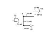
- the net in the schematic wiring data D1 will be described with reference to FIG.
- FIG. 2 is an image diagram of the net in the schematic wiring data D1.
- the net in this specification refers to a wiring network to all gates to which a signal output from a certain gate (logic circuit) is input, as indicated by a thick line in FIG.
- the signal output from the AND gate G1 is input to the buffers G2 and G3
- the wiring from the AND gate G1 to the buffers G2 and G3 is an example of a net.
- the schematic wiring data D1 includes information on wiring segments (partial wiring) in the x-axis and y-axis directions and connection points between the segments in the x-axis direction and the segments in the y-axis direction in each net. On the other hand, the schematic wiring data D1 does not include information on the wiring layer used for each segment.
- the net shown in FIG. 2 extends in the x-axis direction (hereinafter referred to as the x-axis direction) segments (partial wirings) S1, S3, S4, S6 and the y-axis direction (hereinafter referred to as the y-axis direction).
- Direction) segments S2 and S5 and the connection point between the x-axis direction segment and the y-axis direction segment and the connection point V between the segment and the gate.
- the target net selection unit 102 selects a net having a reference wiring length D3 or more from the wiring length data D2 of each net.
- a priority-targeted netlist D4 is created.
- priorities are assigned in order from the net having the longest wiring length, and the wiring layers are preferentially assigned by the wiring layer determining unit 103 from the net having the longest wiring length. This is because a net having a longer total wiring length has a larger wiring delay, and thus has a large influence on variations in signal delay (total of gate delay and wiring delay), and an improvement effect is also increased.
- the wiring layer determination unit 103 for the target net allocates a wiring layer for each segment in the net using the schematic wiring data D1 in order from the net with the highest priority in the target net list with priority D4. As a result, detailed wiring data in which the data of the used wiring layer is added to the target nets listed in the priority-target net list D4 is obtained.
- the wiring layer determination unit 103 for the target net calculates an index ⁇ that indicates how evenly a plurality of usable wiring layers are allocated in the target net for each combination of the segment and the wiring layer. . Then, according to the calculation result of the index ⁇ , a wiring layer is assigned to each segment so that a plurality of usable wiring layers are equalized. This is one of the most important points in the present invention, and details on the index ⁇ and the like will be described later.
- FIG. 3A is a diagram according to an example of the present embodiment, and is an example of detailed wiring data D5 corresponding to the schematic wiring data D1 of the net shown in FIG.
- three wiring layers M1 to M3 are used.
- a wiring layer M1 is assigned to the segments S1, S4, and S6, a wiring layer M2 is assigned to the segments S2 and S5, and a wiring layer M3 is assigned to the segment S3.
- the reason why the wiring layer M1 is allocated to the segments S1, S4, and S6 is that the wiring layer connected to the normal gate is a common wiring layer.
- the odd-numbered wiring layers M1, M3, are stacked in order from the bottom to the top. Even-numbered wiring layers M2, M4,... are used for the segments in the y-axis direction. Alternatively, if even-numbered wiring layers M2, M4,... Are used for the segments in the x-axis direction, odd-numbered wiring layers M1, M3,. Furthermore, as shown in FIG. 3A, normally, adjacent segments connected by vias (contacts) located at each connection point V are composed of upper and lower adjacent wiring layers.
- the wiring layer determination unit 104 allocates a wiring layer using the general wiring data D1 for all nets other than the target net to which the wiring layer is allocated by the wiring layer determination unit 103. Thereby, detailed wiring data D6 for all nets is obtained.
- the detailed wiring data D6 is data in which a wiring layer is assigned to each segment in each net. For example, the wiring layer determination unit 104 simply assigns the wiring layer M1 to the segment in the x-axis direction and assigns the wiring layer M2 to the segment in the y-axis direction.
- FIG. 4 is a block diagram of a wiring device for a semiconductor integrated circuit according to a comparative example of the first embodiment.
- the wiring device of the semiconductor integrated circuit according to the comparative example does not have a configuration surrounded by a dotted line in FIG. That is, the wiring layer determination unit 104 only assigns a wiring layer to each segment of all nets based on the schematic wiring data D1. Thereby, detailed wiring data D6 for all nets is obtained.
- the wiring layer determination unit 104 simply assigns the wiring layer M1 to the segment in the x-axis direction and assigns the wiring layer M2 to the segment in the y-axis direction.
- FIG. 3B is a diagram according to a comparative example of the present embodiment, and is an example of detailed wiring data D6 corresponding to the net schematic wiring data D1 shown in FIG.
- three wiring layers M1 to M3 can be used, but the wiring layer M1 is used for the segments S1, S3, S4, and S6 in the x-axis direction, and the wiring layer M2 is used for the segments S2 and S5 in the y-axis direction. Is assigned. That is, in FIG. 3A, the wiring layer M3 is assigned to the segment S3, whereas in FIG. 3B, the wiring layer M1 is assigned to the segment S3.
- the basic concept in the processing here is that in the target net selected by the target net selection unit 102 in order to reduce the variation in signal delay due to the manufacturing variation of the wiring, “as many wiring layers as possible, Use as evenly as possible. "
- the wiring delay varies by that amount due to variations in the shape of the wiring composed of the wiring layer. This is because variations in wiring resistance and capacitance, which are causes of wiring delay variation, are determined by wiring shape variations.
- the variation in shape is, for example, a variation in wiring width due to exposure or etching, or a variation in wiring film thickness due to film formation or CMP (Chemical-Mechanical-Polishing).
- the probability that the wiring capacity increases simultaneously in all the wiring layers of the net is reduced. Furthermore, the wiring layers may cancel each other's variations. Therefore, the variation in wiring delay is reduced. Specifically, when the wiring capacitance is dominant as a factor that determines the wiring delay, the wiring layer with the net varies in the direction of increasing the capacitance, and other wiring layers vary so that the capacitance decreases. Variations in total capacity are reduced. As a result, the amount of statistical variation (standard deviation and variance) of the wiring delay is reduced.
- the wiring capacitance is dominant as a cause of the wiring delay as described above. This is mainly true when the total net wiring length is relatively short. In this case, it can be considered that the wiring delay is simply proportional to the wiring capacity.
- the average wiring capacity C0 per unit length and its standard deviation ⁇ 0 are constant regardless of the location and wiring layer, and the wiring capacity per unit length of different wiring layers
- the correlation coefficient r0 (0 ⁇ r0 ⁇ 1) is constant.
- the average wiring capacity C0, the standard deviation ⁇ 0, and the correlation coefficient r0 are values determined from the measurement data. Assume that the total wiring length L of a certain net is a constant value.
- the wiring layers that can be used in the net are M1, M2,..., Mn (n: natural number), and the total wiring length for each wiring layer is L1, L2,. That is, the total wiring length of the usable wiring layer Mi (i: natural number and 1 ⁇ i ⁇ n) is Li.
- the wiring delay T when the variation is not taken into consideration is expressed by Expression (1), where ⁇ is a constant.
- i a natural number
- 1 ⁇ i ⁇ n L.
- the variance ⁇ (T) 2 of the wiring delay T is expressed by the equation (2).
- an appropriate wiring layer is assigned to each segment of the target net so that the index ⁇ expressed by Expression (3) is minimized.
- the index ⁇ indicates how evenly a plurality of wiring layers are allocated in the wiring.
- the connected segments need to be adjacent wiring layers (of course).
- the wiring layers are as shown in FIG. 3A. It is determined. For this reason, the wiring delay variation is smaller in FIG. 3A according to the present embodiment using the wiring layers M1, M2, and M3 than in FIG. 3B according to the comparative example using the wiring layers M1 and M2.
- the number of vias (that is, connection point V) connecting the wiring layers is the same, and the total wiring length does not change. Therefore, the wiring delay without considering the variation can be regarded as the same. it can.
- the used wiring layer is determined so as to avoid a wiring layer that has already been determined and arranged (a net having a higher wiring layer assignment order than the signal wiring, such as a power supply wiring and a clock wiring). .
- FIG. 5A is a diagram related to an example of the present embodiment, and is an example of the detailed wiring data D5.
- FIG. 5B is a diagram according to a comparative example of the present embodiment, and is an example of detailed wiring data D6.
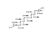
- the two inverters G11 and G12 include segments S11, S13, S15, S17, and S19 extending in the x-axis direction and segments S12, S14, S16, S18, and 10 extending in the y-axis direction. It is composed of a number of vias V.
- r0 0 in equation (2).
- the wiring layer M1 is assigned to the segments S11, S13, S15, S17, and S19
- the wiring layer M2 is assigned to the segments S12, S14, S16, and S18 as shown in FIG. 5B according to the comparative example.
- the ratio ⁇ (T) / T of the wiring delay variation to the wiring delay is calculated as in the expression (4).
- the wiring layer M1 is provided in the segments S11 and S19
- the wiring layer M2 is provided in the segments S12 and S18
- the wiring layer M3 is provided in the segments S13 and S17
- the wiring layer M4 is provided in the segments S14 and S16.
- the wiring layer M5 is allocated to the segment S15.
- FIG. 6 is a graph showing a comparison of the wiring delay variation widths of the example and the comparative example.
- a general 3 ⁇ is used as the variation width.
- the wiring delay variation width of the net formed of a single wiring layer is ⁇ 20%.
- the guard bandwidth in the design is reduced and the design is facilitated. Furthermore, effects such as design TAT shortening, chip area reduction, power consumption reduction, and performance improvement are expected.
- Expression (6) may be used by determining a certain appropriate coefficient r1 (0 ⁇ r1 ⁇ 1) as a calculation expression of the index ⁇ .
- the coefficient r1 in Expression (6) corresponds to the correlation coefficient r0 in Expression (2).
- equation (2) it was assumed that capacity was dominant over delay.
- Expression (6) the designer may set an appropriate coefficient r1 in consideration of the relationship between the capacitance, resistance, and wiring delay. Similar to the case of Expression (3), appropriate wiring layers are assigned to all the segments so that the index ⁇ is minimized. Many other formulas for calculating the index ⁇ are conceivable and are not limited to the formulas (3) and (6).
- Li ′ ⁇ i ⁇ Li (7)
- ⁇ i of the wiring layer with small variation is set small, and ⁇ i of the wiring layer with large variation is set large.
- the wiring layer with small variation is used longer than the wiring layer with large variation.
- Modification 3 of Embodiment 1 instead of setting the net having the reference wiring length D3 or more as the target net, the number of target nets may be determined in advance, and the wiring layers may be determined in order from the net having the longest total wiring length.
- Modification 4 of Embodiment 1 Instead of using the net having the reference wiring length D3 or more as the target net, a net designated in advance by the designer may be used as the target net. Alternatively, the reference wiring length D3 according to the first embodiment and the number of modifications 3 may be used together. This is effective when a designer can predict a net in which delay variation is a problem in timing convergence.
- an upper limit value may be set in advance for the index ⁇ .
- the number of wiring layers to be used may be reduced as long as the index ⁇ is not more than the upper limit value, instead of using as many wiring layers as possible.
- the wiring layer to be used may be determined again. As a result, an unnecessary increase in the number of used wiring layers can be avoided, so that the number of application target nets can be increased and the wiring process can be shortened.
- the upper limit value of the index ⁇ may be provided in stages. For example, all nets may be divided into several groups according to the total wiring length, and an upper limit value of the index ⁇ to be satisfied by the net belonging to the group may be provided for each group. Here, a smaller upper limit is set as the total wiring length is longer. When the modification 4 is used together, the upper limit value of the index ⁇ is set for each net designated by the designer.
- FIG. 7 is a block diagram of a wiring device for a semiconductor integrated circuit according to the second embodiment.
- the semiconductor integrated circuit wiring device according to the second embodiment includes a segment length calculation unit 201 and a division target segment selection unit 202.
- Each data D7 to D11 is stored in a storage device (not shown).
- one wiring layer is assigned to each segment acquired from the schematic wiring data D1.
- one segment acquired from the schematic wiring data D1 is further divided into a plurality of segments, and a wiring layer for each divided segment is assigned.
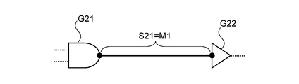
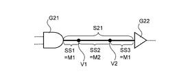
- one segment S21 shown in FIG. 8A acquired from the schematic wiring data D1 is usually composed of one wiring layer as shown in FIG. 8B.
- the segment S21 is composed of the wiring layer M1.
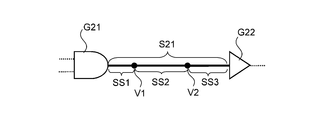
- segment division positions V1 and V2 as shown in FIG. 9A are provided for the segment S21 of FIG. 8A acquired from the schematic wiring data D1, and the segment S21 is a new segment SS1. , SS2, SS3.
- segment length data D7 of each segment is obtained.
- the segment selection segment 202 selects all segments whose segment length ratio (segment length / wiring length) in the net wiring length is equal to or greater than the reference value D8 from the segment length data D7 of each segment. As a result, a segment target segment list D9 is created. This is because a segment having a larger proportion of the total wiring length of the net is likely to become an obstacle to reducing the wiring delay variation.
- the segment dividing unit 203 sequentially divides the segments listed in the division target segment list D9 using a predetermined division ratio designation value D10. Thereby, segment division position data D11 is obtained. That is, as shown in FIG. 9A, segment division positions V1 and V2 are provided for the segment S21, and the segment S21 is divided into new segments SS1, SS2, and SS3.
- the predetermined division ratio designation value D10 is, for example, “provide one point at a position where a segment is divided into 1: 1” or “provide two points at a position where a segment is divided into 1: 1: 1 or 1: 2: 1”. It is specified data. Alternatively, the designer may arbitrarily designate the division ratio without the division ratio designation value D10.
- the wiring layer determination unit 103 assigns a wiring layer to each of the divided new segments determined from the segment division position data D11 using the same method as in the first embodiment.
- M1, M2, and M1 are respectively assigned to new segments SS1, SS2, and SS3 divided from the segment S21.
- the wiring layer M2 that should be mainly used in the y-axis direction is exceptionally used in the x-axis direction.
- the net between the AND gate G21 and the buffer G22 is composed of one segment S21. Of course, the same applies to one segment in a net composed of a plurality of segments. Can be divided into new segments.
- FIG. 10 is a graph showing a comparison of the wiring delay variation widths of the example and the comparative example.
- a general 3 ⁇ is used as an index of variation width.
- the wiring delay variation is reduced.
- a limit is set for the number of segment division positions set, that is, the number of vias.
- the upper limit value of the number of usable vias is determined in advance in proportion to the total wiring length of the net. If the number of vias in the net has already exceeded the upper limit as a result of rough wiring, segment division is not performed. If not, segment division is performed until the number of vias reaches the upper limit.
- the order in which the segments are divided is the order of the segment length / wiring length.
- the upper limit value of the number of vias is set to be proportional to the total wiring length of the net, but may be set to be proportional to the unit path length.
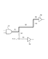
- FIG. 11 is a diagram for explaining a unit route. As indicated by a thick line in FIG. 11, the unit path is a path without a branch connecting one gate to one gate, and is a part of the net. When determining whether the number of vias exceeds the upper limit value, this unit path length is used instead of the total net wiring length in the first modification. For a signal path, the resistance of the branch does not affect the signal delay of that path. For this reason, it is considered more reasonable to examine the effect of increased resistance due to the addition of vias for each unit route than to the net.
- the segment division position is set in that unit route.
- the segment is not targeted for segment division.
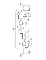
- FIG. 12 is a diagram for explaining a path. As indicated by a thick line in FIG. 12, a path is all nets included in a path connecting adjacent flip-flops. In FIG. 12, the network includes five nets N1 to N5 that form a path connecting the flip-flop FF1 and the flip-flop FF2. Note that in this specification, a flip-flop is included in a gate.
- the net N1 is a wiring from the flip-flop FF1 to the AND gate G31 and the buffer G32.
- the net N2 is a wiring from the AND gate G31 to the buffers G33 and G34.
- the net N3 is a wiring from the buffer G34 to the AND gate G35.
- the net N4 is a wiring from the AND gate G35 to the buffers G36 and G37.
- the net N5 is a wiring from the buffer G36 to the flip-flop FF2.
- the assignment of wiring layers by the wiring layer determination unit 103 in FIGS. 1 and 7 is performed in order from the path having the largest total wiring length.
- the wiring layer assigned to the net in the path having the longest total wiring length is not changed in the assignment of wiring layers of other paths. If this is applied to the fourth modification of the first embodiment, the designer can select the critical path assumed in the design as it is, and it is easier than selecting a net that may cause a problem. Further, in the timing verification after the detailed wiring by the wiring layer determination unit 104 in FIG. 1 or FIG. 7, the designer selects the path as it is when redesigning the path whose timing cannot be converged due to the wiring delay variation. Can do.
- the detailed wiring data D5 of the target net is first created prior to the creation of the detailed wiring data D6 in FIGS. 1 and 7, the detailed wiring data D5 of the target net is first created.
- the present invention may be applied as a correction means for the existing detailed wiring data D6.
- the target net may be selected from the detailed wiring data D6, and the wiring layer assigned to the segment in the net may be changed.
- the segment may be further divided into a plurality of segments, and the wiring layer assigned to the divided segments may be changed.
- the segment can be divided and changed among the divided segments as in the second embodiment. What is necessary is just to change the wiring layer. If the segment division position cannot be changed at a predetermined ratio, it may be changed at the closest ratio. Of course, you may correct the wiring layer of the segment of the other net which is obstructing. Furthermore, when selecting a target net, a net included in a path in which a timing error has occurred due to wiring delay variation as a result of timing verification may be set as the target net.
Landscapes
- Engineering & Computer Science (AREA)
- Computer Hardware Design (AREA)
- Physics & Mathematics (AREA)
- Theoretical Computer Science (AREA)
- Computer Networks & Wireless Communication (AREA)
- Evolutionary Computation (AREA)
- Geometry (AREA)
- General Engineering & Computer Science (AREA)
- General Physics & Mathematics (AREA)
- Design And Manufacture Of Integrated Circuits (AREA)
Abstract
複数のゲート間を結ぶ信号配線を、複数のセグメントに分割し、前記複数のセグメントのそれぞれに対して、n層(nは2以上の整数)の配線層のいずれか1つを少なくとも1回ずつ割り当てる半導体集積回路の配線方法であって、前記n層の配線層の割り当てに際し、前記複数のセグメントと前記n層の配線層との組み合わせから、前記n層の配線層が前記信号配線においてどの程度均等に割り当てられるかを示す指数を計算し、前記指数の計算結果に応じて、前記複数のセグメントに対して前記n層の配線層が均等になるように割り当てる半導体集積回路の配線方法である。これにより、半導体集積回路の配線遅延ばらつきを低減できる。
Description
本発明は、半導体集積回路の配線方法及び配線装置に関する。
LSI(Large Scale Integrated Curcuit)の微細化が進展するほど、配線の幅や膜厚などの配線形状のチップ間ばらつき(製造ばらつき)に起因した配線抵抗値や配線容量値のばらつきが大きくなる。また、配線抵抗及び配線容量に起因する配線遅延は、ゲート遅延ほど微細化の恩恵を享受できないため、微細化とともに信号遅延に占める配線遅延の割合が大きくなる。以上のことから、配線遅延ばらつきによる信号遅延ばらつきが大きくなり、回路設計が難しくなっている。従って、配線遅延ばらつきを低減可能な設計手法が希求されている。
特許文献1には、クロックスキューを低減するため、使用する配線層の大部分を同一配線層にしたクロックツリーが開示されている。同一配線層からなる配線同士であれば、その配線遅延は、製造ばらつきにより、同じように変動する。具体的には、製造ばらつきにより、ある配線の配線遅延が設計値より大きくなった場合、その配線と同一の配線層からなる他の配線の配線遅延も設計値より大きくなる。小さくなった場合も同様である。ここで、特許文献1の図1に示されるように、元々クロックツリーの各パスは同じ配線長になるように配置されている。そのため、使用する配線層を同一配線層にすれば、クロックツリーのパス間の遅延差(つまり、クロックスキュー)のばらつきは小さくなる。
また、特許文献2には、クロックスキューを低減するため、延長配線を付加することにより、各パスに使用する複数の配線層の使用比率をパス間で揃えたクロックツリーが開示されている。各パスに使用する複数の配線層の使用比率をパス間で揃えれば、各パスの配線遅延は、製造ばらつきにより、同じように変動する。従って、特許文献1と同様の理由から、クロックスキューのばらつきは小さくなる。
なお、特許文献3には、複数の配線層を有し、各配線層からなる配線の配線密度を全体として均等化した半導体装置が開示されている。しかし、上述の配線遅延ばらつきを低減可能なものではない。
発明者は以下の課題を見出した。
クロック配線は、通常の信号配線よりも優先して配線される。そのため、特許文献1及び2に開示されたように、各パスを同じ配線長にしたり、各パスに使用する複数の配線層の使用比率をパス間で揃えたりすることができる。つまり、クロック配線については、配線層や配線長、配線のレイアウトなどにおける自由度が大きい。他方、通常の信号配線は、クロック配線や電源配線の後にレイアウトされる。ここで、チップ面積を最小化するため、通常の信号配線については、配線層や配線長、配線のレイアウトなどにおける自由度が小さい。そのため、特許文献1及び2をそのまま信号配線へ適用することは難しかった。
クロック配線は、通常の信号配線よりも優先して配線される。そのため、特許文献1及び2に開示されたように、各パスを同じ配線長にしたり、各パスに使用する複数の配線層の使用比率をパス間で揃えたりすることができる。つまり、クロック配線については、配線層や配線長、配線のレイアウトなどにおける自由度が大きい。他方、通常の信号配線は、クロック配線や電源配線の後にレイアウトされる。ここで、チップ面積を最小化するため、通常の信号配線については、配線層や配線長、配線のレイアウトなどにおける自由度が小さい。そのため、特許文献1及び2をそのまま信号配線へ適用することは難しかった。
さらに、そもそも特許文献1及び2では、クロックスキュー(パス間の配線遅延の「差」)のばらつきを小さくすることはできたとしても、クロック配線における配線遅延自体のばらつきを低減することはできなかった。従って、特許文献1及び2により、信号配線おける配線遅延ばらつきを低減することもできなかった。
本発明に係る半導体集積回路の配線方法は、
複数のゲート間を結ぶ信号配線を、複数のセグメントに分割し、
前記複数のセグメントのそれぞれに対して、n層(nは2以上の整数)の配線層のいずれか1つを少なくとも1回ずつ割り当てる半導体集積回路の配線方法であって、
前記n層の配線層の割り当てに際し、
前記複数のセグメントと前記n層の配線層との組み合わせから、前記n層の配線層が前記信号配線においてどの程度均等に割り当てられるかを示す指数を計算し、
前記指数の計算結果に応じて、前記複数のセグメントに対して前記n層の配線層が均等になるように割り当てるものである。
複数のゲート間を結ぶ信号配線を、複数のセグメントに分割し、
前記複数のセグメントのそれぞれに対して、n層(nは2以上の整数)の配線層のいずれか1つを少なくとも1回ずつ割り当てる半導体集積回路の配線方法であって、
前記n層の配線層の割り当てに際し、
前記複数のセグメントと前記n層の配線層との組み合わせから、前記n層の配線層が前記信号配線においてどの程度均等に割り当てられるかを示す指数を計算し、
前記指数の計算結果に応じて、前記複数のセグメントに対して前記n層の配線層が均等になるように割り当てるものである。
本発明に係る半導体集積回路の配線装置は、
複数のゲート間を結ぶ信号配線が複数のセグメントに分割された配線データが、格納された記憶部と、
前記複数のセグメントのそれぞれに対して、n層(nは2以上の整数)の配線層のいずれか1つを少なくとも1回ずつ割り当てる配線層決定部と、を備え、
前記配線層決定部は、
前記複数のセグメントと前記n層の配線層との組み合わせから、前記n層の配線層が前記信号配線においてどの程度均等に割り当てられるかを示す指数を計算し、
前記指数の計算結果に応じて、前記複数のセグメントに対して前記n層の配線層が均等になるように割り当てるものである。
複数のゲート間を結ぶ信号配線が複数のセグメントに分割された配線データが、格納された記憶部と、
前記複数のセグメントのそれぞれに対して、n層(nは2以上の整数)の配線層のいずれか1つを少なくとも1回ずつ割り当てる配線層決定部と、を備え、
前記配線層決定部は、
前記複数のセグメントと前記n層の配線層との組み合わせから、前記n層の配線層が前記信号配線においてどの程度均等に割り当てられるかを示す指数を計算し、
前記指数の計算結果に応じて、前記複数のセグメントに対して前記n層の配線層が均等になるように割り当てるものである。
本発明では、複数のセグメントとn層の配線層との組み合わせから、n層の配線層が信号配線においてどの程度均等に割り当てられるかを示す指数を計算し、
指数の計算結果に応じて、複数のセグメントに対してn層の配線層が均等になるように割り当てる。そのため、配線遅延ばらつきを低減することができる。
指数の計算結果に応じて、複数のセグメントに対してn層の配線層が均等になるように割り当てる。そのため、配線遅延ばらつきを低減することができる。
本発明によれば、配線遅延ばらつきが低減された半導体集積回路の配線方法及び配線装置を提供することができる。
以下、本発明を適用した具体的な実施の形態について、図面を参照しながら詳細に説明する。ただし、本発明が以下の実施の形態に限定される訳ではない。また、説明を明確にするため、以下の記載及び図面は、適宜、簡略化されている。
(実施の形態1)
図1を参照して本発明の第1の実施の形態に係る半導体集積回路の配線装置について説明する。図1は、実施の形態1に係る半導体集積回路の配線装置のブロック図である。図1に示すように、この半導体集積回路の配線装置は、例えばLSIのロジック部の自動配置配線装置である。この半導体集積回路の配線装置は、配線長算出部101、対象ネット選択部102、対象ネット用の配線層決定部103、対象ネット以外のネット用の配線層決定部104、概略配線データD1、配線長データD2、基準配線長D3、優先順位付き対象ネットリストD4、対象ネットの詳細配線データD5、全ネットの詳細配線データD6を備えている。各データD1~D6は、図示されない記憶装置に格納されている。
図1を参照して本発明の第1の実施の形態に係る半導体集積回路の配線装置について説明する。図1は、実施の形態1に係る半導体集積回路の配線装置のブロック図である。図1に示すように、この半導体集積回路の配線装置は、例えばLSIのロジック部の自動配置配線装置である。この半導体集積回路の配線装置は、配線長算出部101、対象ネット選択部102、対象ネット用の配線層決定部103、対象ネット以外のネット用の配線層決定部104、概略配線データD1、配線長データD2、基準配線長D3、優先順位付き対象ネットリストD4、対象ネットの詳細配線データD5、全ネットの詳細配線データD6を備えている。各データD1~D6は、図示されない記憶装置に格納されている。
配線長算出部101は、概略配線データD1から各ネットの配線長を算出する。これにより、各ネットの配線長データD2が得られる。ここで、図2を用いて、概略配線データD1におけるネットについて説明する。図2は、概略配線データD1におけるネットのイメージ図である。本明細書におけるネットとは、図2において太線で示されたように、あるゲート(論理回路)から出力された信号が入力される全てのゲートまでの配線網をいう。具体的には、図2では、ANDゲートG1から出力された信号はバッファG2、G3に入力され、ANDゲートG1からバッファG2、G3までの配線が、ネットの一例である。ここで、概略配線データD1は、各ネットにおけるx軸及びy軸方向の配線セグメント(部分配線)、x軸方向のセグメントとy軸方向のセグメントとの接続点の情報を含んでいる。一方、概略配線データD1には、各セグメントに使用する配線層の情報は含まれていない。
ここで、図2に示されたネットは、x軸方向に延びた(以下、x軸方向の)セグメント(部分配線)S1、S3、S4、S6とy軸方向に延びた(以下、y軸方向の)セグメントS2、S5、x軸方向のセグメントとy軸方向のセグメントとの接続点及びセグメントとゲートとの接続点Vから構成されている。図2に示されたネットは、黒丸で示された8つの接続点Vを有している。セグメントS1の長さをL(S1)などとすると、図2に示されたネットの配線長LはL=L(S1)+L(S2)+L(S3)+L(S4)+L(S5)+L(S6)となる。
対象ネット選択部102は、各ネットの配線長データD2から基準配線長D3以上のネットを選択する。これにより、優先順位付き対象ネットリストD4が作成される。ここで、優先順位付き対象ネットリストD4において、配線長が長いネットから順に優先順位が付されており、配線長が長いネットから優先的に配線層決定部103により配線層が割り当てられる。これは、総配線長が長いネットほど、配線遅延が大きいため、信号遅延(ゲート遅延と配線遅延の合計)のばらつきに及ぼす影響も大きく、改善効果も大きくなるためである。
対象ネット用の配線層決定部103は、優先順位付き対象ネットリストD4において優先順位の高いネットから順に、概略配線データD1を用いて、ネットにおけるセグメント毎に配線層を割り当てる。これにより、優先順位付き対象ネットリストD4に挙げられた対象ネットに対して使用配線層のデータが付加された詳細配線データが得られる。ここで、対象ネット用の配線層決定部103は、セグメントと配線層との組み合わせのそれぞれについて、使用可能な複数の配線層が対象ネットにおいてどの程度均等に割り当てられるかを示す指数βを計算する。そして、指数βの計算結果に応じて、使用可能な複数の配線層が均等になるように、各セグメントに対して配線層を割り当てる。この点は、本発明において最も重要な点の1つであり、指数β等についての詳細は後述する。
詳細配線データD5は、各ネットにおいて各セグメントに対して配線層が割り当てられたデータである。図3Aは、本実施の形態の実施例に係る図であって、図2に示されたネットの概略配線データD1に対応する詳細配線データD5の一例である。図3Aでは、3つの配線層M1~M3が使用されている。そして、セグメントS1、S4、S6には配線層M1が、セグメントS2、S5には配線層M2が、セグメントS3には配線層M3が割り当てられている。ここで、セグメントS1、S4、S6に配線層M1が割り当てられるのは、通常ゲートに接続される配線層は共通の配線層だからである。
一般的に、配線層M1、M2、・・・、Mnが下から上へ順に積層されているとすると、x軸方向のセグメントには奇数番目の配線層M1、M3、・・・を用い、y軸方向のセグメントには偶数番目の配線層M2、M4、・・・を用いる。あるいは、x軸方向のセグメントに偶数番目の配線層M2、M4、・・・を用いれば、y軸方向のセグメントに奇数番目の配線層M1、M3、・・・を用いる。さらに、図3Aに示されるように、通常、各接続点Vに位置するビア(コンタクト)により接続された隣接するセグメントは上下に隣接する配線層から構成される。
配線層決定部104は、配線層決定部103により配線層が割り当てられた対象ネット以外の全てのネットについて、概略配線データD1を用いて配線層を割り当てる。これにより、全てのネットに対する詳細配線データD6が得られる。詳細配線データD6は、各ネットにおける各セグメントに対して配線層が割り当てられたデータである。配線層決定部104は、例えば、単純にx軸方向のセグメントに対して配線層M1を、y軸方向のセグメントに対して配線層M2を割り当てる。
次に、図4を用いて、実施の形態1の比較例に係る半導体集積回路の配線装置について説明する。図4は、実施の形態1の比較例に係る半導体集積回路の配線装置のブロック図である。比較例に係る半導体集積回路の配線装置は、図1において点線で囲まれた構成を有していない。つまり、配線層決定部104が、概略配線データD1に基づいて、全ネットの各セグメントに対して配線層を割り当てるのみである。これにより、全てのネットに対する詳細配線データD6が得られる。配線層決定部104は、例えば、単純にx軸方向のセグメントに対して配線層M1を、y軸方向のセグメントに対して配線層M2を割り当てる。
図3Bは、本実施の形態の比較例に係る図であって、図2に示されたネットの概略配線データD1に対応する詳細配線データD6の一例である。図3Bでも、3つの配線層M1~M3が使用可能であるが、x軸方向のセグメントS1、S3、S4、S6には配線層M1が、y軸方向のセグメントS2、S5には配線層M2が割り当てられている。つまり、図3Aでは、セグメントS3に配線層M3が割り当てられているのに対し、図3Bでは、セグメントS3に配線層M1が割り当てられている。
次に、対象ネット用の配線層決定部103での処理の詳細について説明する。ここでの処理における基本的概念は、配線の製造ばらつきに起因した信号遅延のばらつきを低減するために、対象ネット選択部102により選択された対象ネットにおいて、「可能な限り多くの配線層を、可能な限り均等な配分で使用する」というものである。
この理由を以下に述べる。あるネットに単一の配線層だけ用いた場合、その配線層からなる配線の形状ばらつきにより、配線遅延はその分だけばらつく。これは配線遅延ばらつきの要因である配線抵抗及び容量のばらつきが配線の形状ばらつきによって決定されるためである。ここで、形状ばらつきとは、例えば、露光やエッチングによる配線幅のばらつきや成膜やCMP(Chemical Mechanical Polishing)による配線膜厚のばらつきなどである。
これに対し、そのネットの配線長を変えずに多数の配線層を用いた場合、ネットの全配線層において同時に配線容量が大きくなるようにばらつく確率は小さくなる。さらに、各配線層が互いのばらつきをキャンセルし合う場合もある。そのため、配線遅延のばらつきは小さくなる。具体的には、配線遅延を決める要因として配線容量が支配的な場合、ネットのある配線層は容量が大きくなる方向にばらつき、他の配線層は容量が小さくなるようにばらつくと、そのネットの総容量のばらつきは小さくなる。結果として、配線遅延の統計的なばらつき量(標準偏差や分散)は小さくなる。
以下に、数式を用いて説明する。議論を簡略化するために、上述の通り、配線遅延の要因として配線容量が支配的な場合を考える。これは、主にネットの総配線長が比較的短い場合に当てはまる。この場合、配線遅延は簡易的に配線容量に比例すると考えることができる。また、やはり議論の簡略化のために、単位長さあたりの平均配線容量C0とその標準偏差σ0は箇所や配線層によらず一定であり、異なる配線層の単位長さあたりの配線容量同士の相関係数r0(0≦r0<1)は一定であるとする。ここで、平均配線容量C0、標準偏差σ0、相関係数r0は、測定データから定まる値である。今、あるネットの総配線長Lが一定値であるとする。そのネットで使用可能な配線層をM1、M2、・・・、Mn(n:自然数)とし、それらの配線層毎の総配線長をL1、L2、・・・、Lnとする。つまり、使用可能な配線層Mi(i:自然数かつ1≦i≦n)の総配線長をLiとする。このとき、ばらつきを考慮しない場合の配線遅延Tは、αをある定数として、式(1)で表される。
T=α・Σ(Li・C0)=α・L・C0 (1)
ここで、iは自然数かつ1≦i≦nであり、ΣLi=Lである。
従って、配線遅延Tの分散σ(T)2は式(2)で表される。

T=α・Σ(Li・C0)=α・L・C0 (1)
ここで、iは自然数かつ1≦i≦nであり、ΣLi=Lである。
従って、配線遅延Tの分散σ(T)2は式(2)で表される。
ここで、jは自然数かつ1≦j≦nである。上述の通り、0≦r0<1であるから、式(2)は、あるiに対してLi=L、j≠iなるjに対してLj=0のとき最大となり、L1=L2=・・・=Ln=L/nのとき最小となる。通常は両者の中間的な状態であるが、「可能な限り多くの配線層を、可能な限り均等な配分で使用する」ことにより、後者に近づけ、配線遅延のばらつきを低減できる。
なお、式(2)において仮にr0=1とすると、σ(T)2=α・σ02・L2となり、配線遅延ばらつきは、使用する配線層の数やその長さの配分に無関係となる。しかしながら、通常は、r0=0.4程度であるため、効果は十分に期待できる。以上の議論において、分かり易くするために行ったいくつかの仮定は効果の本質を損ねるものではなく、実際にも同様の効果が得られる。
本実施の形態では、式(3)で表される指数βが最小となるように、対象ネットの各セグメントに対して、適切な配線層を割り当てる。ここで、指数βは、複数の配線層が配線においてどの程度均等に割り当てられているかを示す。
β=Σ(Li2)/(ΣLi)2=Σ(Li2)/L2 (3)
β=Σ(Li2)/(ΣLi)2=Σ(Li2)/L2 (3)
この際に、配線層の選択にあたっては、接続されるセグメント同士は(当然ながら)隣接した配線層同士となっている必要がある。式(3)の指数βは、式(2)におけるr0=0の場合の、配線遅延に対する配線ばらつきの比率を表現する値であるが、実際にはr0>0であっても、式(3)の最小化により配線遅延ばらつきは低減される。
その結果、図2に示されたネットにおいて、上述の通り、使用可能な配線層が3つの配線層M1、M2、M3である場合(n=3の場合)、図3Aのように配線層が決定される。配線層M1、M2を使用した比較例に係る図3Bよりも配線層M1、M2、M3を使用した本実施の形態に係る図3Aの方が、上記理由から配線遅延ばらつきは小さくなる。ここで、図3Bと図3Aとでは、配線層間を接続するビア(つまり接続点V)の個数は同じであり、総配線長も変わらないため、ばらつきを考慮しない配線遅延は同一とみなすことができる。なお、使用配線層は、既に配線層が決定され、配置されている配線(電源配線、クロック配線などのように信号配線よりも配線層割り当て順位が上位のネット)を回避するように決定される。
次に、図5A、5Bを用いて、実施の形態1の他の実施例及び比較例について説明する。図5Aは、本実施の形態の実施例に係る図であって、詳細配線データD5の一例である。図5Bは、本実施の形態の比較例に係る図であって、詳細配線データD6の一例である。図5A、5Bに示すように、2つのインバータG11、G12が、x軸方向に延びたセグメントS11、S13、S15、S17、S19とy軸方向に延びたセグメントS12、S14、S16、S18、10個のビアVから構成されている。各セグメントの長さは、中央のセグメントS15以外のセグメントは全て長さ1、セグメントS15はその倍の長さ2であるとする。つまり、L=10とする。ここで、式(2)におけるr0=0である場合を考える。
比較例に係る図5Bのように、セグメントS11、S13、S15、S17、S19に配線層M1が、セグメントS12、S14、S16、S18に配線層M2が割り当てられたとする。このとき、L1=6、L2=4となる。式(1)、式(2)、r0=0、L=10から、配線遅延ばらつきの配線遅延に対する割合σ(T)/Tは式(4)のように計算される。
σ(T)/T
=sqrt(α2・σ02・Σ(Li2))/α・L・C0
=σ0/C0・sqrt(62+42)/10
=0.72・σ0/C0 (4)
σ(T)/T
=sqrt(α2・σ02・Σ(Li2))/α・L・C0
=σ0/C0・sqrt(62+42)/10
=0.72・σ0/C0 (4)
一方、実施例に係る図5Aのように、セグメントS11、S19に配線層M1が、セグメントS12、S18に配線層M2が、セグメントS13、S17に配線層M3が、セグメントS14、S16に配線層M4が、セグメントS15に配線層M5が、割り当てられたとする。このとき、L1=L2=L3=L4=L5=2となる。式(1)、式(2)、r0=0、L=10から、配線遅延ばらつきの配線遅延に対する割合σ(T)/Tは式(5)のように計算される。
σ(T)/T
=σ0/C0・sqrt(22+22+22+22+22)/10
=0.45・σ0/C0 (5)
従って、実施例は比較例と比べ、配線遅延ばらつき幅が、0.45/0.72=0.62倍に縮小される(つまり、ばらつき幅が38%削減される)。
σ(T)/T
=σ0/C0・sqrt(22+22+22+22+22)/10
=0.45・σ0/C0 (5)
従って、実施例は比較例と比べ、配線遅延ばらつき幅が、0.45/0.72=0.62倍に縮小される(つまり、ばらつき幅が38%削減される)。
図6は、実施例及び比較例の配線遅延ばらつき幅を比較して示したグラフである。ここで、ばらつき幅として一般的な3σを用いて考える。例えば、単一配線における単位長さあたりの容量値の3σが20%(3×σ0/C0=0.2)であるとする。つまり、配線容量ばらつき幅が±20%であるとする。このとき、式(1)から配線容量と配線遅延とは比例関係にあるから、単一配線層からなるネットの配線遅延ばらつき幅も±20%となる。
図6に示すように、図5Bの比較例における配線遅延ばらつき3×σ(T)/Tは、式(4)及び3×σ0/C0=0.2から0.72×0.2=0.144となる。つまり、配線遅延ばらつき幅は±14.4%となる。これに対し、図5Aの実施例における配線遅延ばらつき3×σ(T)/Tは、式(4)及び3×σ0/C0=0.2から0.45×0.2=0.09となる。つまり、配線遅延ばらつき幅は±9%となる。配線遅延ばらつき幅が削減されることにより、設計におけるガードバンド幅が小さくなり、設計が容易となる。さらに、設計TAT短縮、チップ面積削減、消費電力削減、性能向上などの効果が見込まれる。
(実施の形態1の変形例1)
式(3)に代わり、指数βの計算式として、ある適当な係数r1(0≦r1<1)を定めて、式(6)を用いてもよい。

式(6)の係数r1は、式(2)における相関係数r0に相当するものである。式(2)では、容量が遅延に対して支配的であると仮定していた。式(6)では、設計者が、容量、抵抗と配線遅延の関係を総合的に考慮して適切な係数r1を設定すればよい。式(3)の場合と同様に、指数βが最小になるように、全てのセグメントに対して、適切な配線層を割り当てる。なお、指数βの計算式は他にも多く考えられ、式(3)や式(6)に限定されるものではない。
式(3)に代わり、指数βの計算式として、ある適当な係数r1(0≦r1<1)を定めて、式(6)を用いてもよい。
(実施の形態1の変形例2)
式(3)及び(6)では、全ての配線層を同等に扱っていた。しかしながら、実際には、配線層によって膜厚や最小配線幅、絶縁膜の比誘電率が異なる場合があり、結果として容量や抵抗、それらのばらつきが異なる。そこで、容量や抵抗、ばらつきの小さい配線層を優先的に使う場合のために、配線層毎の重み付け係数γi(0≦γi)をあらかじめ設定しておく。次式(7)で計算されるLi’を、式(3)や式(6)のLiに代入することによりβを求める。
Li’=γi・Li (7)
例えば、ばらつきの小さい配線層のγiは小さく、ばらつきの大きい配線層のγiは大きく設定される。これにより、ばらつきの小さい配線層はばらつきの大きい配線層よりも長く使われることになる。
式(3)及び(6)では、全ての配線層を同等に扱っていた。しかしながら、実際には、配線層によって膜厚や最小配線幅、絶縁膜の比誘電率が異なる場合があり、結果として容量や抵抗、それらのばらつきが異なる。そこで、容量や抵抗、ばらつきの小さい配線層を優先的に使う場合のために、配線層毎の重み付け係数γi(0≦γi)をあらかじめ設定しておく。次式(7)で計算されるLi’を、式(3)や式(6)のLiに代入することによりβを求める。
Li’=γi・Li (7)
例えば、ばらつきの小さい配線層のγiは小さく、ばらつきの大きい配線層のγiは大きく設定される。これにより、ばらつきの小さい配線層はばらつきの大きい配線層よりも長く使われることになる。
(実施の形態1の変形例3)
基準配線長D3以上のネットを対象ネットとする代わりに、あらかじめ対象ネットの個数を定めておき、総配線長が長いネットから順に配線層を決定していってもよい。
基準配線長D3以上のネットを対象ネットとする代わりに、あらかじめ対象ネットの個数を定めておき、総配線長が長いネットから順に配線層を決定していってもよい。
(実施の形態1の変形例4)
基準配線長D3以上のネットを対象ネットとする代わりに、設計者があらかじめ指定したネットを対象ネットとしてもよい。または、実施の形態1に係る基準配線長D3や変形例3の個数と併用してもよい。設計者があらかじめ遅延ばらつきがタイミング収束において問題となるネットを予想できる場合に有効である。
基準配線長D3以上のネットを対象ネットとする代わりに、設計者があらかじめ指定したネットを対象ネットとしてもよい。または、実施の形態1に係る基準配線長D3や変形例3の個数と併用してもよい。設計者があらかじめ遅延ばらつきがタイミング収束において問題となるネットを予想できる場合に有効である。
(実施の形態1の変形例5)
指数βが小さいほど配線遅延ばらつきは小さくなるため、指数βにあらかじめ上限値を設けてもよい。その上で、各セグメントの配線層を決定する際に、できる限り多くの配線層を使用するのではなく、指数βが上限値以下となる範囲で、使用する配線層数を減らしてもよい。ここで、使用しない配線層を先に指定した後、指数βの値を確認し、上限値を超えていれば、使用する配線層を決定し直してもよい。これにより、不必要な使用配線層の増加を回避できるため、適用対象ネット数を増やしたり、配線工程を短縮したりすることができる。
指数βが小さいほど配線遅延ばらつきは小さくなるため、指数βにあらかじめ上限値を設けてもよい。その上で、各セグメントの配線層を決定する際に、できる限り多くの配線層を使用するのではなく、指数βが上限値以下となる範囲で、使用する配線層数を減らしてもよい。ここで、使用しない配線層を先に指定した後、指数βの値を確認し、上限値を超えていれば、使用する配線層を決定し直してもよい。これにより、不必要な使用配線層の増加を回避できるため、適用対象ネット数を増やしたり、配線工程を短縮したりすることができる。
また、指数βの上限値を段階的に設けてもよい。例えば、全ネットを総配線長によりいくつかのグループに分け、グループ毎にそのグループに属するネットが満たすべき指数βの上限値を設けてもよい。ここで、総配線長が長いほど小さな上限値を設定する。変形例4を併用する場合、設計者が指定するネットごとに指数βの上限値を設定する。
(実施の形態2)
次に、図7を用いて、本発明の第2の実施の形態に係る半導体集積回路の配線装置について説明する。図7は、実施の形態2に係る半導体集積回路の配線装置のブロック図である。図7に示すように、実施の形態2に係る半導体集積回路の配線装置は、実施の形態1に係る半導体集積回路の配線装置の構成に加え、セグメント長算出部201、分割対象セグメント選択部202、セグメント分割部203、セグメント長データD7、セグメント長/配線長の基準値D8、分割対象セグメントリストD9、分割比率指定値D10、セグメント分割位置データD11を備えている。各データD7~D11は、図示されない記憶装置に格納されている。
次に、図7を用いて、本発明の第2の実施の形態に係る半導体集積回路の配線装置について説明する。図7は、実施の形態2に係る半導体集積回路の配線装置のブロック図である。図7に示すように、実施の形態2に係る半導体集積回路の配線装置は、実施の形態1に係る半導体集積回路の配線装置の構成に加え、セグメント長算出部201、分割対象セグメント選択部202、セグメント分割部203、セグメント長データD7、セグメント長/配線長の基準値D8、分割対象セグメントリストD9、分割比率指定値D10、セグメント分割位置データD11を備えている。各データD7~D11は、図示されない記憶装置に格納されている。
実施の形態1では、概略配線データD1から取得したセグメント毎に1つの配線層を割り当てた。これに対し、実施の形態2では、概略配線データD1から取得した1つのセグメントをさらに複数のセグメントに分割し、分割されたセグメント毎の配線層を割り当てる。
具体的には、概略配線データD1から取得される図8Aに示される1つのセグメントS21は、通常、図8Bに示すように、1つの配線層で構成される。図8Bの例では、セグメントS21が配線層M1から構成されている。これに対して、本実施の形態では、概略配線データD1から取得される図8AのセグメントS21に対して、図9Aに示すようなセグメント分割位置V1、V2を設け、セグメントS21を新たなセグメントSS1、SS2、SS3に分割する。
図7のセグメント長算出部201は、概略配線データD1から各セグメントのセグメント長を算出する。これにより、各セグメントのセグメント長データD7が得られる。
分割対象セグメント選択部202は、各セグメントのセグメント長データD7からネットの配線長に占めるそのセグメント長の割合(セグメント長/配線長)が基準値D8以上である全てのセグメントを選択する。これにより、分割対象セグメントリストD9が作成される。ここで、ネットの総配線長に占める割合が大きいセグメントほど、配線遅延ばらつき低減の障害になり易いためである。
分割対象セグメント選択部202は、各セグメントのセグメント長データD7からネットの配線長に占めるそのセグメント長の割合(セグメント長/配線長)が基準値D8以上である全てのセグメントを選択する。これにより、分割対象セグメントリストD9が作成される。ここで、ネットの総配線長に占める割合が大きいセグメントほど、配線遅延ばらつき低減の障害になり易いためである。
セグメント分割部203は、分割対象セグメントリストD9にリストアップされたセグメントに対し、所定の分割比率指定値D10を用いて順に分割していく。これにより、セグメント分割位置データD11が得られる。つまり、図9Aに示すように、セグメントS21に対しセグメント分割位置V1、V2が設けられ、セグメントS21が新たなセグメントSS1、SS2、SS3へ分割される。所定の分割比率指定値D10は、例えば、「セグメントを1:1に分割する位置に1点設ける」や「1:1:1や1:2:1に分割する位置に2点設ける」などと規定されたデータである。あるいは、分割比率指定値D10なしに、設計者が任意に分割比率を指定してもよい。
そして、配線層決定部103は、実施の形態1と同様の手法を用いて、セグメント分割位置データD11から定まる分割された新たなセグメントのそれぞれに対して、配線層を割り当てる。例えば、図9Bでは、セグメントS21から分割された新たなセグメントSS1、SS2、SS3に対し、それぞれM1、M2、M1が割り当てられている。これにより、多くの配線層を、均等に割り当てやすくなるため、配線遅延ばらつきは低減する。ただし、この例では主にy軸方向に用いられるはずの配線層M2が、例外的にx軸方向で使用されることになる。なお、図9A、9Bでは、ANDゲートG21及びバッファG22間のネットが、1つのセグメントS21から構成されているが、当然のことながら、複数のセグメントから構成されるネットにおける1つのセグメントについても同様に新たなセグメントに分割することができる。
図9A、9Bでは、セグメントS21を1:2:1に分割する位置に2点のセグメント分割位置(配線層切換位置)が設けられている。実施の形態1と同様の仮定のもとに、同様の計算を行うことにより、図8A、8Bに示された比較例、図9A、9Bに示された実施例による配線遅延ばらつきの配線遅延に対する割合σ(T)/Tは、それぞれ式(7)、式(8)のようになる。
σ(T)/T
=σ0/C0・sqrt(42)/4
=σ0/C0 (7)
σ(T)/T
=σ0/C0・sqrt(22+22)/(2+2)
=0.71・σ0/C0 (8)
従って、ばらつき幅は、0.71/1=0.71倍に縮小される(ばらつき幅が29%削減される)。
σ(T)/T
=σ0/C0・sqrt(42)/4
=σ0/C0 (7)
σ(T)/T
=σ0/C0・sqrt(22+22)/(2+2)
=0.71・σ0/C0 (8)
従って、ばらつき幅は、0.71/1=0.71倍に縮小される(ばらつき幅が29%削減される)。
図10は、実施例及び比較例の配線遅延ばらつき幅を比較して示したグラフである。ここで、ばらつき幅の指標として一般的な3σを用いて考える。例えば、単一配線における単位長さあたりの容量値の3σが20%(3×σ0/C0=0.2)であるとする。
図10に示すように、図8Bの比較例における配線遅延ばらつき3×σ(T)/Tは、式(7)及び3×σ0/C0=0.2から1×0.2=0.2となる。つまり、配線遅延ばらつき幅は±20%となる。これに対し、図9Bの実施例における配線遅延ばらつき3×σ(T)/Tは、式(8)及び3×σ0/C0=0.2から0.71×0.2=0.142となる。つまり、配線遅延ばらつき幅は±14.2%となる。本実施の形態においても、実施の形態1と同様の効果が見込まれる。
図10に示すように、図8Bの比較例における配線遅延ばらつき3×σ(T)/Tは、式(7)及び3×σ0/C0=0.2から1×0.2=0.2となる。つまり、配線遅延ばらつき幅は±20%となる。これに対し、図9Bの実施例における配線遅延ばらつき3×σ(T)/Tは、式(8)及び3×σ0/C0=0.2から0.71×0.2=0.142となる。つまり、配線遅延ばらつき幅は±14.2%となる。本実施の形態においても、実施の形態1と同様の効果が見込まれる。
(実施の形態2の変形例1)
実施の形態2では、配線遅延ばらつきは低減される。一方、セグメント分割位置に設けられるビアにより抵抗が増加するため、配線遅延自体が増加する。そこで、セグメント分割位置の設定数、すなわちビア増加数に対する制限を設ける。ここで、セグメント分割位置が1点増えると、ビアも1個増える。あらかじめ、ネットの総配線長に比例して、使用可能なビア個数の上限値を決めておく。概略配線の結果、ネットのビア個数が既に上限値を超えている場合、セグメント分割は行わない。超えていない場合、ビア個数が上限値に達するまで、セグメント分割を行なう。セグメント分割を行う順番は、セグメント長/配線長が大きい順とする。
実施の形態2では、配線遅延ばらつきは低減される。一方、セグメント分割位置に設けられるビアにより抵抗が増加するため、配線遅延自体が増加する。そこで、セグメント分割位置の設定数、すなわちビア増加数に対する制限を設ける。ここで、セグメント分割位置が1点増えると、ビアも1個増える。あらかじめ、ネットの総配線長に比例して、使用可能なビア個数の上限値を決めておく。概略配線の結果、ネットのビア個数が既に上限値を超えている場合、セグメント分割は行わない。超えていない場合、ビア個数が上限値に達するまで、セグメント分割を行なう。セグメント分割を行う順番は、セグメント長/配線長が大きい順とする。
(実施の形態2の変形例2)
実施の形態2の変形例1では、ビア個数の上限値をネットの総配線長に比例するように設定したが、単位経路長に比例するように設定してもよい。図11は、単位経路を説明するための図である。図11に太線で示すように、単位経路とは、1つのゲートから1つのゲートまでを結ぶ分岐の無い経路であって、ネットの一部である。ビア個数が上限値を超えているかどうかを判断する際に、変形例1におけるネットの総配線長に代わり、この単位経路長を用いる。ある信号経路にとって、枝分かれ部分の抵抗は、その経路の信号遅延には影響しない。そのため、ビア追加による抵抗増加の影響は、ネットよりも単位経路毎に検討する方が合理的であると考えられる。
実施の形態2の変形例1では、ビア個数の上限値をネットの総配線長に比例するように設定したが、単位経路長に比例するように設定してもよい。図11は、単位経路を説明するための図である。図11に太線で示すように、単位経路とは、1つのゲートから1つのゲートまでを結ぶ分岐の無い経路であって、ネットの一部である。ビア個数が上限値を超えているかどうかを判断する際に、変形例1におけるネットの総配線長に代わり、この単位経路長を用いる。ある信号経路にとって、枝分かれ部分の抵抗は、その経路の信号遅延には影響しない。そのため、ビア追加による抵抗増加の影響は、ネットよりも単位経路毎に検討する方が合理的であると考えられる。
ある単位経路に対するビア個数が上限値を超えていない場合、その単位経路内でセグメント分割位置の設定を行う。複数の単位経路が同一のセグメントを共有している場合、そのうちのある経路のビア個数が上限値を超えていれば、そのセグメントはセグメント分割の対象とはしない。
実施の形態1、実施の形態1の変形例1~5、実施の形態2では、「ネット」を対象といているが、「パス」を対象としてもよい。つまり、ネット単位で配線層の割り当てを最適化するのではなく、パス単位で配線層の割り当てを最適化する。図12は、パスを説明するための図である。図12に太線で示すように、パスとは、隣接するフリップフロップ間を繋ぐ経路に含まれる全ネットである。図12では、フリップフロップFF1とフリップフロップFF2とを繋ぐパスを構成する5つのネットN1~N5からなる。なお、本明細書において、フリップフロップはゲートに含まれる。
ここで、図12に示すように、ネットN1はフリップフロップFF1からANDゲートG31及びバッファG32に至る配線である。ネットN2はANDゲートG31からバッファG33及びG34に至る配線である。ネットN3はバッファG34からANDゲートG35に至る配線である。ネットN4はANDゲートG35からバッファG36及びG37に至る配線である。ネットN5はバッファG36からフリップフロップFF2に至る配線である。
図1や図7における配線層決定部103による配線層の割り当ては、総配線長が大きいパスから順に行う。複数のパスで1つのネットを共有している場合、その中で最も総配線長が長いパスにおいてそのネットに割り当てられた配線層は、他のパスの配線層の割り当てにおいては変更しない。これを実施の形態1の変形例4に適用すれば、設計者が設計上想定されるクリティカルパスをそのまま選択でき、問題となり得るネットを選択するよりも容易である。さらに、図1や図7における配線層決定部104による詳細配線後のタイミング検証において、配線遅延ばらつきによりタイミング収束できなかったパスを、再設計の際に、設計者が当該パスをそのまま選択することができる。
なお、上記実施の形態において説明した方法は、LSIのロジック部の自動配置配線のみでなく、ロジック部以外の回路設計、自動でない回路設計にも適用可能である。
また、上記実施の形態では、図1や図7における詳細配線データD6の作成に先立ち、まず対象ネットの詳細配線データD5を作成している。しかしながら、既在の詳細配線データD6に対する修正手段として、本発明を適用してもよい。具体的には、詳細配線データD6から対象ネットを選択し、そのネットにおけるセグメントに割り当てられた配線層を変更すればよい。あるいは、実施の形態2のように、セグメントをさらに複数のセグメントに分割して、分割されたセグメントに割り当てられた配線層を変更してもよい。
例えば、他のネットの配線が障害になり、1つのセグメント全体の配線層を変更することができなければ、実施の形態2と同様に、そのセグメントを分割し、分割されたセグメントのうち変更可能なものの配線層を変更すればよい。セグメント分割位置は、あらかじめ決められた比率で変更できなければ、最もそれに近い比率で変更すればよい。もちろん、障害になっている他のネットのセグメントの配線層の方を修正してもよい。さらに、対象ネットを選択する際、タイミング検証の結果、配線遅延ばらつきが原因でタイミングエラーを生じているパスに含まれるネットを対象ネットとしてもよい。
以上、実施の形態を参照して本願発明を説明したが、本願発明は上記によって限定されるものではない。本願発明の構成や詳細には、発明のスコープ内で当業者が理解し得る様々な変更をすることができる。
この出願は、2011年4月5日に出願された日本出願特願2011-097021を基礎とする優先権を主張し、その開示の全てをここに取り込む。
101 配線長算出部
102 対象ネット選択部
103 配線層決定部
104 配線層決定部
201 セグメント長算出部
202 分割対象セグメント選択部
203 セグメント分割部
D1 概略配線データ
D2 配線長データ
D3 基準配線長
D4 対象ネットリスト
D5 詳細配線データ
D6 詳細配線データ
D7 セグメント長データ
D8 基準値
D9 分割対象セグメントリスト
D10 分割比率指定値
D11 セグメント分割位置データ
FF1、FF2 フリップフロップ
G1、G21、G31、G35 ANDゲート
G2、G3、G22、G32、G33、G34、G36、G37 バッファ
G11、G12 インバータ
M1-Mn 配線層
N1-N5 ネット
S1-S6、S11-S19、S21 セグメント
SS1-SS3 セグメント
102 対象ネット選択部
103 配線層決定部
104 配線層決定部
201 セグメント長算出部
202 分割対象セグメント選択部
203 セグメント分割部
D1 概略配線データ
D2 配線長データ
D3 基準配線長
D4 対象ネットリスト
D5 詳細配線データ
D6 詳細配線データ
D7 セグメント長データ
D8 基準値
D9 分割対象セグメントリスト
D10 分割比率指定値
D11 セグメント分割位置データ
FF1、FF2 フリップフロップ
G1、G21、G31、G35 ANDゲート
G2、G3、G22、G32、G33、G34、G36、G37 バッファ
G11、G12 インバータ
M1-Mn 配線層
N1-N5 ネット
S1-S6、S11-S19、S21 セグメント
SS1-SS3 セグメント
Claims (20)
- 複数のゲート間を結ぶ信号配線を、複数のセグメントに分割し、
前記複数のセグメントのそれぞれに対して、n層(nは2以上の整数)の配線層のいずれか1つを少なくとも1回ずつ割り当てる半導体集積回路の配線方法であって、
前記n層の配線層の割り当てに際し、
前記複数のセグメントと前記n層の配線層との組み合わせから、前記n層の配線層が前記信号配線においてどの程度均等に割り当てられるかを示す指数を計算し、
前記指数の計算結果に応じて、前記複数のセグメントに対して前記n層の配線層が均等になるように割り当てる半導体集積回路の配線方法。 - 前記n層の配線層の割り当てに際し、
長さが長い前記信号配線から順に、前記n層の配線層の割り当てを実行することを特徴とする請求項1に記載の半導体集積回路の配線方法。 - 前記n層の配線層の割り当てに際し、
前記複数のセグメントの少なくとも1つをさらに複数の新たなセグメントに分割し、当該新たなセグメントのそれぞれに対して、前記n層の配線層の割り当てを実行することを特徴とする請求項1又は2に記載の半導体集積回路の配線方法。 - 前記配線層決定部は、
互いに接続された隣接するセグメントには、互いに隣接した配線層を割り当てることを特徴とする請求項1~3のいずれか一項に記載の半導体集積回路の配線方法。 - 前記n層の配線層の割り当てに際し、
前記複数のゲートのそれぞれに接続されたセグメントには、いずれも同一の配線層を割り当てることを特徴とする請求項1~4のいずれか一項に記載の半導体集積回路の配線方法。 - 前記信号配線は、互いに隣接する前記複数のゲート間を結ぶネットであることを特徴とする請求項1~5のいずれかに一項に記載の半導体集積回路の配線方法。
- 前記複数のゲートは、2つのフリップフロップであり、
前記信号配線は、互いに隣接する前記2つのフリップフロップ間を結ぶパスであることを特徴とする請求項1~5のいずれか一項に記載の半導体集積回路の配線方法。 - 前記指数をβとして、次式により与えられることを特徴とする請求項1~7のいずれか一項に記載の半導体集積回路の配線方法。

- 前記係数r=0として前記指数βを計算することを特徴とする請求項8に記載の半導体集積回路の配線方法。
- 前記指数βが最小となる前記組み合わせにより前記n層の配線層の割り当てを実行することを特徴とする請求項8又は9に記載の半導体集積回路の配線方法。
- 複数のゲート間を結ぶ信号配線が複数のセグメントに分割された配線データが、格納された記憶部と、
前記複数のセグメントのそれぞれに対して、n層(nは2以上の整数)の配線層のいずれか1つを少なくとも1回ずつ割り当てる配線層決定部と、を備え、
前記配線層決定部は、
前記複数のセグメントと前記n層の配線層との組み合わせから、前記n層の配線層が前記信号配線においてどの程度均等に割り当てられるかを示す指数を計算し、
前記指数の計算結果に応じて、前記複数のセグメントに対して前記n層の配線層が均等になるように割り当てる半導体集積回路の配線装置。 - 前記信号配線の長さを算出する配線長算出部を更に備え、
前記配線層決定部は、前記配線長算出部により算出された長さが長い前記信号配線から順に、前記n層の配線層の割り当てを実行することを特徴とする請求項11に記載の半導体集積回路の配線装置。 - 前記複数のセグメントの少なくとも1つをさらに複数の新たなセグメントに分割するセグメント分割部を更に備え、
前記配線層決定部は、当該新たなセグメントのそれぞれに対して、前記n層の配線層の割り当てを実行することを特徴とする請求項11又は12に記載の半導体集積回路の配線装置。 - 前記配線層決定部は、
互いに接続された隣接するセグメントには、互いに隣接した配線層を割り当てることを特徴とする請求項11~13のいずれか一項に記載の半導体集積回路の配線装置。 - 前記配線層決定部は、
前記複数のゲートのそれぞれに接続されたセグメントには、いずれも同一の配線層を割り当てることを特徴とする請求項11~14のいずれか一項に記載の半導体集積回路の配線装置。 - 前記信号配線は、互いに隣接する前記複数のゲート間を結ぶネットであることを特徴とする請求項11~15のいずれかに一項に記載の半導体集積回路の配線装置。
- 前記複数のゲートは、2つのフリップフロップであり、
前記信号配線は、互いに隣接する前記2つのフリップフロップ間を結ぶパスであることを特徴とする請求項11~15のいずれか一項に記載の半導体集積回路の配線装置。 - 前記指数をβとして、次式により与えられることを特徴とする請求項11~17のいずれか一項に記載の半導体集積回路の配線装置。

- 前記配線層決定部は、
前記係数r=0として前記指数βを計算することを特徴とする請求項18に記載の半導体集積回路の配線装置。 - 前記配線層決定部は、
前記指数βが最小となる前記組み合わせにより前記n層の配線層の割り当てを実行することを特徴とする請求項18又は19に記載の半導体集積回路の配線装置。
Applications Claiming Priority (2)
| Application Number | Priority Date | Filing Date | Title |
|---|---|---|---|
| JP2011-097021 | 2011-04-25 | ||
| JP2011097021 | 2011-04-25 |
Publications (1)
| Publication Number | Publication Date |
|---|---|
| WO2012147285A1 true WO2012147285A1 (ja) | 2012-11-01 |
Family
ID=47071819
Family Applications (1)
| Application Number | Title | Priority Date | Filing Date |
|---|---|---|---|
| PCT/JP2012/002415 Ceased WO2012147285A1 (ja) | 2011-04-25 | 2012-04-06 | 半導体集積回路の配線方法及び配線装置 |
Country Status (1)
| Country | Link |
|---|---|
| WO (1) | WO2012147285A1 (ja) |
Citations (2)
| Publication number | Priority date | Publication date | Assignee | Title |
|---|---|---|---|---|
| JPS6148071A (ja) * | 1984-08-10 | 1986-03-08 | インタ−ナショナル ビジネス マシ−ンズ コ−ポレ−ション | 布線方法 |
| JP2006209702A (ja) * | 2005-01-31 | 2006-08-10 | Nec Electronics Corp | 半導体装置設計プログラム |
-
2012
- 2012-04-06 WO PCT/JP2012/002415 patent/WO2012147285A1/ja not_active Ceased
Patent Citations (2)
| Publication number | Priority date | Publication date | Assignee | Title |
|---|---|---|---|---|
| JPS6148071A (ja) * | 1984-08-10 | 1986-03-08 | インタ−ナショナル ビジネス マシ−ンズ コ−ポレ−ション | 布線方法 |
| JP2006209702A (ja) * | 2005-01-31 | 2006-08-10 | Nec Electronics Corp | 半導体装置設計プログラム |
Similar Documents
| Publication | Publication Date | Title |
|---|---|---|
| US9477801B2 (en) | Multi-threaded track assignment | |
| CN110297782B (zh) | 仲裁系统和方法 | |
| US20060281221A1 (en) | Enhanced routing grid system and method | |
| CN110705204B (zh) | 基于多阶段策略的时序感知层分配方法 | |
| Zhou et al. | Optimal river routing with crosstalk constraints | |
| US10831972B2 (en) | Capacity model for global routing | |
| WO2007149927A2 (en) | System and method for designing a common centroid layout for an integrated circuit | |
| US8495534B2 (en) | Post-placement cell shifting | |
| CN115983187B (zh) | 基于多策略的考虑总线偏差的层分配方法 | |
| US20190065636A1 (en) | Layout of large block synthesis blocks in integrated circuits | |
| Chang et al. | Obstacle-aware group-based length-matching routing for pre-assignment area-I/O flip-chip designs | |
| CN116341473A (zh) | 超大规模集成电路下时延驱动的层分配方法 | |
| CN116887079B (zh) | 层次分析法资源均衡虚拟数据中心光网络映射方法及系统 | |
| US8347257B2 (en) | Detailed routability by cell placement | |
| US9678530B2 (en) | Clock skew adjusting structure | |
| CN116127906B (zh) | 先进通孔柱技术下高性能层分配方法 | |
| Liu et al. | Incremental layer assignment for timing optimization | |
| US20090125860A1 (en) | Auto-Routing Small Jog Eliminator | |
| US5872719A (en) | Method of wiring semiconductor integrated circuit and semiconductor integrated circuit | |
| US10839130B1 (en) | Metal layer routing based on grid regions | |
| JP3705737B2 (ja) | 半導体集積回路のレイアウト方法 | |
| Zhong et al. | Whitespace insertion for through-silicon via planning on 3-D SoCs | |
| CN112784521A (zh) | 先进制程下时延驱动的层分配方法 | |
| Mo et al. | Fishbone: a block-level placement and routing scheme | |
| JP3548398B2 (ja) | 概略経路決定方法および概略経路決定方式 |
Legal Events
| Date | Code | Title | Description |
|---|---|---|---|
| 121 | Ep: the epo has been informed by wipo that ep was designated in this application |
Ref document number: 12776759 Country of ref document: EP Kind code of ref document: A1 |
|
| NENP | Non-entry into the national phase |
Ref country code: DE |
|
| 122 | Ep: pct application non-entry in european phase |
Ref document number: 12776759 Country of ref document: EP Kind code of ref document: A1 |
|
| NENP | Non-entry into the national phase |
Ref country code: JP |