WO2012144018A1 - Boost converter control device - Google Patents
Boost converter control device Download PDFInfo
- Publication number
- WO2012144018A1 WO2012144018A1 PCT/JP2011/059651 JP2011059651W WO2012144018A1 WO 2012144018 A1 WO2012144018 A1 WO 2012144018A1 JP 2011059651 W JP2011059651 W JP 2011059651W WO 2012144018 A1 WO2012144018 A1 WO 2012144018A1
- Authority
- WO
- WIPO (PCT)
- Prior art keywords
- phase
- boost converter
- motor
- voltage
- frequency
- Prior art date
Links
Images


Classifications
-
- H—ELECTRICITY
- H02—GENERATION; CONVERSION OR DISTRIBUTION OF ELECTRIC POWER
- H02M—APPARATUS FOR CONVERSION BETWEEN AC AND AC, BETWEEN AC AND DC, OR BETWEEN DC AND DC, AND FOR USE WITH MAINS OR SIMILAR POWER SUPPLY SYSTEMS; CONVERSION OF DC OR AC INPUT POWER INTO SURGE OUTPUT POWER; CONTROL OR REGULATION THEREOF
- H02M3/00—Conversion of dc power input into dc power output
- H02M3/02—Conversion of dc power input into dc power output without intermediate conversion into ac
- H02M3/04—Conversion of dc power input into dc power output without intermediate conversion into ac by static converters
- H02M3/10—Conversion of dc power input into dc power output without intermediate conversion into ac by static converters using discharge tubes with control electrode or semiconductor devices with control electrode
- H02M3/145—Conversion of dc power input into dc power output without intermediate conversion into ac by static converters using discharge tubes with control electrode or semiconductor devices with control electrode using devices of a triode or transistor type requiring continuous application of a control signal
- H02M3/155—Conversion of dc power input into dc power output without intermediate conversion into ac by static converters using discharge tubes with control electrode or semiconductor devices with control electrode using devices of a triode or transistor type requiring continuous application of a control signal using semiconductor devices only
- H02M3/156—Conversion of dc power input into dc power output without intermediate conversion into ac by static converters using discharge tubes with control electrode or semiconductor devices with control electrode using devices of a triode or transistor type requiring continuous application of a control signal using semiconductor devices only with automatic control of output voltage or current, e.g. switching regulators
-
- H—ELECTRICITY
- H02—GENERATION; CONVERSION OR DISTRIBUTION OF ELECTRIC POWER
- H02P—CONTROL OR REGULATION OF ELECTRIC MOTORS, ELECTRIC GENERATORS OR DYNAMO-ELECTRIC CONVERTERS; CONTROLLING TRANSFORMERS, REACTORS OR CHOKE COILS
- H02P6/00—Arrangements for controlling synchronous motors or other dynamo-electric motors using electronic commutation dependent on the rotor position; Electronic commutators therefor
- H02P6/10—Arrangements for controlling torque ripple, e.g. providing reduced torque ripple
-
- H—ELECTRICITY
- H02—GENERATION; CONVERSION OR DISTRIBUTION OF ELECTRIC POWER
- H02P—CONTROL OR REGULATION OF ELECTRIC MOTORS, ELECTRIC GENERATORS OR DYNAMO-ELECTRIC CONVERTERS; CONTROLLING TRANSFORMERS, REACTORS OR CHOKE COILS
- H02P21/00—Arrangements or methods for the control of electric machines by vector control, e.g. by control of field orientation
- H02P21/05—Arrangements or methods for the control of electric machines by vector control, e.g. by control of field orientation specially adapted for damping motor oscillations, e.g. for reducing hunting
-
- H—ELECTRICITY
- H02—GENERATION; CONVERSION OR DISTRIBUTION OF ELECTRIC POWER
- H02M—APPARATUS FOR CONVERSION BETWEEN AC AND AC, BETWEEN AC AND DC, OR BETWEEN DC AND DC, AND FOR USE WITH MAINS OR SIMILAR POWER SUPPLY SYSTEMS; CONVERSION OF DC OR AC INPUT POWER INTO SURGE OUTPUT POWER; CONTROL OR REGULATION THEREOF
- H02M1/00—Details of apparatus for conversion
- H02M1/0067—Converter structures employing plural converter units, other than for parallel operation of the units on a single load
- H02M1/007—Plural converter units in cascade
-
- H—ELECTRICITY
- H02—GENERATION; CONVERSION OR DISTRIBUTION OF ELECTRIC POWER
- H02M—APPARATUS FOR CONVERSION BETWEEN AC AND AC, BETWEEN AC AND DC, OR BETWEEN DC AND DC, AND FOR USE WITH MAINS OR SIMILAR POWER SUPPLY SYSTEMS; CONVERSION OF DC OR AC INPUT POWER INTO SURGE OUTPUT POWER; CONTROL OR REGULATION THEREOF
- H02M7/00—Conversion of ac power input into dc power output; Conversion of dc power input into ac power output
- H02M7/42—Conversion of dc power input into ac power output without possibility of reversal
- H02M7/44—Conversion of dc power input into ac power output without possibility of reversal by static converters
- H02M7/48—Conversion of dc power input into ac power output without possibility of reversal by static converters using discharge tubes with control electrode or semiconductor devices with control electrode
Definitions
- the present invention relates to a technical field of a boost converter control device that controls a boost converter in a motor drive system for driving a three-phase AC motor.
- Patent Document 1 In this kind of technical field, one that reduces voltage fluctuation has been proposed (for example, see Patent Document 1). According to the voltage converter disclosed in Patent Document 1, when the absolute value of the reactor current of the boost converter is small, it is possible to reduce the voltage fluctuation due to the influence of dead time by lowering the carrier frequency of the boost converter. It is said that there is.
- An inverter as a power converter installed between a boost converter that boosts a DC voltage supplied from a DC power supply and an electric load such as a motor usually includes a smoothing capacitor for voltage smoothing.
- the smoothing capacitor has a larger capacity and is less susceptible to voltage fluctuations and is stable, but the cost and physique increase. Therefore, for example, in a situation where there are not a few restrictions on installation space, cost, etc., such as drive control of a vehicle drive motor, there is a tendency to reduce the capacity of the smoothing capacitor.
- the voltage control circuit of the boost converter Is constructed as a PI control circuit composed of a proportional element (P) and an integral element (I), and cannot compensate for a 90-degree phase delay caused by a smoothing capacitor. For this reason, the voltage fluctuation of the smoothing capacitor cannot be suppressed in real time.
- the voltage control circuit of the boost converter is a PID control circuit in which a differential element (D) is added to the above-described configuration. Since the differential element has a phase advance characteristic of 90 degrees, the voltage fluctuation in the frequency band corresponding to the motor electrical frequency can be suitably suppressed by the PID control realized by the PID control circuit.
- D differential element
- the differential element generally has a larger control term (D term) in the higher frequency band.
- Voltage fluctuations that occur in the terminal voltage of the smoothing capacitor are roughly classified into at least two types, one is voltage fluctuations in the frequency band corresponding to the motor electrical frequency described above, and the other is the switching frequency of the inverter (several k to several tens of kHz). ) In the frequency band corresponding to (). Therefore, the differential element follows the switching ripple more than the voltage fluctuation in the frequency band corresponding to the motor electrical frequency.
- the frequency band of the switching ripple is in a region that exceeds the control speed of the input / output current of the DC power supply. If the differential element tries to follow the switching ripple in this way, the terminal voltage of the smoothing capacitor tends to become unstable. .
- the present invention has been made in view of such technical problems, and in a motor drive system including a boost converter and a power converter between a DC power source and an electrical load, a smoothing capacitor of the power converter is provided.
- An object of the present invention is to provide a control device for a boost converter capable of reducing the capacity without increasing the withstand voltage.
- a control device for a boost converter is provided between a DC power source, a three-phase AC motor, and the DC power source and the three-phase AC motor, and the three-phase AC motor.
- a power converter comprising a switching circuit corresponding to each of the three phases and a smoothing capacitor arranged in parallel with the switching circuit, and installed between the power converter and the DC power source,
- a boost converter control apparatus for controlling the boost converter in a motor drive system including a boost converter that boosts a DC voltage of a DC power source and supplies the boosted voltage to the power converter, and includes a proportional element, an integral element, and a derivative element And the differential element is configured as a band pass filter, and the output voltage of the boost converter is set to the voltage V across the smoothing capacitor.
- Calculating means for calculating a PID control amount corresponding to the current command value of the boost converter for maintaining the command value, and control means for controlling the output voltage of the boost converter based on the calculated PID control amount (Cla
- the boost converter control device means, for example, a computer device, a controller, a processor, or the like that includes a memory or the like as appropriate, and may include various electrical or magnetic elements or circuits as appropriate. is there.
- the control device for the boost converter includes at least a part of a control device that controls and controls other elements (for example, a power converter and a three-phase AC motor) that constitute the entire motor drive system according to the present invention. It may be a shared device.
- the boost converter control device includes a proportional element corresponding to the proportional term (P term), an integral element corresponding to the integral term (I term), and a differential element corresponding to the differential term (D term).
- PID control as a control amount corresponding to the current command value of the boost converter for maintaining or converging the inter-terminal voltage VH of the smoothing capacitor to the command value (hereinafter referred to as “VH command value” as appropriate) by the arithmetic means.
- VH command value a control amount corresponding to the current command value of the boost converter for maintaining or converging the inter-terminal voltage VH of the smoothing capacitor to the command value (hereinafter referred to as “VH command value” as appropriate) by the arithmetic means.
- VH command value the inter-terminal voltage
- the boost converter is driven by PID control as a kind of so-called feedback control under the control of the control means according to the present invention.
- the deviation used in performing this feedback control is preferably a VH command value as a control target determined according to the target torque and target rotation speed of the three-phase AC motor, and a terminal at that time. Deviation from voltage VH.
- the boost converter control device preferably includes a current command value as a PID control amount obtained by a control amount calculation according to the PID control law, and a current value of the boost converter at that time. Based on the deviation, the control amount for maintaining the current value of the boost converter at the current command value (for example, the PI control amount composed of the P term and the I term) is used as a duty signal to be used for comparison with the carrier signal. You may provide the other calculating means to calculate.
- the differential element has a phase advance characteristic of 90 °, and is suitable as an element that compensates for the phase delay of 90 ° generated by the smoothing capacitor. That is, the differential term obtained by the differential element makes it possible to match the phase of the DC current drawn from the DC power source in the process of feedback control with the phase of the power of the three-phase AC motor, and the output voltage of the boost converter ( It is possible to suitably suppress the voltage fluctuation corresponding to the motor electrical frequency generated in the inter-terminal voltage VH). That is, due to the technical idea that PID control is used to control the boost converter, it is not necessary to increase the withstand voltage required for the smoothing capacitor or the switching element of the power converter as the capacity of the smoothing capacitor is reduced. It is possible to reduce the capacity of the smoothing capacitor without increasing the physique.
- the differentiator reacts more sensitively at the higher frequency side, it is used for switching ripples of power converters that fluctuate in the high frequency side of the motor electrical frequency (generally the order differs by about one to two digits).
- the control amount (D term) is more greatly affected.
- the effect of suppressing the voltage fluctuation corresponding to the motor electrical frequency to be suppressed is reduced, and the switching ripple of the power converter cannot be fully tracked. Therefore, the voltage VH between the terminals of the smoothing capacitor may be changed.
- the differential element is configured as a BPF (band pass filter) instead of a normal differentiator.
- the BPF is means for passing a signal in a certain frequency band (which may be variable depending on the design) centered on the cutoff frequency fc, or amplifying it according to a gain that is set as appropriate.
- the BPF has a phase advance characteristic of 90 ° almost the same as that of the differentiator in a part of the low frequency band on the low frequency side from the cut-off frequency fc (specifically, the BPF is low with 90 ° as the upper limit).
- the phase is advanced toward the frequency side).
- BPF is used as a differentiating element as an alternative element of the differentiator, only voltage fluctuation corresponding to the motor electric frequency can be efficiently suppressed depending on the design of the cut-off frequency fc.
- (1) and (2) and the frequency band to which the electric frequency of the motor that defines the frequency characteristics of the voltage fluctuation to be suppressed belong and the frequency band to which the switching ripple of the power converter that should not be originally followed belong Derived from very different things.
- the boost converter control device of the present invention since the differential element for calculating the differential term in the calculation means is BPF, while suppressing the voltage fluctuation corresponding to the motor electrical frequency, the power conversion Excessive reaction to the switching ripple of the vessel can also be suppressed. As a result, the terminal voltage VH of the smoothing capacitor can be stably maintained, so that it is possible to realize a reduction in the capacity of the smoothing capacitor without increasing cost and size.
- the design or setting of the cut-off frequency fc is important.
- the setting band of the cut-off frequency fc that can clearly dominate the effect is so wide that no numerical limitation is required.
- the cutoff frequency of the BPF may be set within the bands shown in the following (1) to (3).
- a band between the physical upper limit value of the motor electrical frequency and the physical lower limit value of the switching frequency of the power converter (as described above, a relatively wide band).
- phase advance amount for example, a phase advance amount of “90 ° ⁇ ” or more
- a band in which a sufficient signal passing amount (for example, a signal passing amount of “0 ⁇ ” dB or more) is ensured with respect to a desired motor electric frequency to be surely suppressed.
- the boost converter is connected between a reactor having one end connected to the positive electrode of the DC power source, and the other end of the reactor and the power converter.
- a second diode is connected between a reactor having one end connected to the positive electrode of the DC power source, and the other end of the reactor and the power converter.
- the output voltage of the boost converter equivalent to the terminal voltage VH of the smoothing capacitor is controlled with relatively good controllability by controlling the switching state of the first and second switching elements. can do. Therefore, voltage fluctuation corresponding to the motor electrical frequency generated in the terminal voltage VH of the smoothing capacitor can be suitably suppressed.
- the current command value of the boost converter is a command value (target value) of the reactor current flowing through the reactor.
- the cut-off frequency of the band-pass filter is equal to or higher than the upper limit value of the motor electrical frequency proportional to the rotational speed of the three-phase AC motor, and the power converter It is less than the lower limit value of the carrier frequency (Claim 3).
- the cutoff frequency of the BPF is set in a frequency range that is not less than the upper limit value of the motor electrical frequency and less than the lower limit value of the carrier frequency of the power converter. Therefore, while ensuring a sufficient phase advance amount and signal passing amount with respect to the motor electrical frequency, it is not following the switching frequency of the switching circuit, which is affected by the carrier frequency of the power converter (for example, inverter). can do. That is, it is possible to effectively suppress only the voltage fluctuation corresponding to the motor electric frequency or to preferentially suppress the voltage fluctuation corresponding to the motor electric frequency.
- the “upper limit value of the motor electrical frequency” in this aspect is not limited to the physical upper limit value that the motor electrical frequency can take.
- the motor electrical frequency is proportional to the number of magnetic pole pairs provided in the three-phase AC motor and the motor rotation speed. Therefore, the physical upper limit value of the motor rotation speed can be a kind of upper limit value of this kind of motor electrical frequency, but in addition, it should be surely suppressed beforehand experimentally, empirically or theoretically. In the case where there is a motor electrical frequency band that has been clarified, the frequency corresponding to the upper limit value of such a band can also be the upper limit value of this type of motor electrical frequency.
- such a “band to be surely suppressed” refers to a relatively high torque at which a three-phase AC motor can output a relatively high torque in view of the relationship between the driving characteristics of the motor and the voltage fluctuation level of the smoothing capacitor.
- a band corresponding to a low rotation region may be used.
- the voltage control means is configured such that, when the rotational speed of the three-phase AC motor is equal to or higher than a predetermined value, the differential element is replaced with the PID control amount. An invalid PI control amount is calculated, and the output control means controls the output voltage based on the calculated PI control amount.
- the PID control using the BPF as a differential element is switched to the PI control that makes the BPF substantially invalid.
- This switching is realized, for example, by changing the differential gain to a value corresponding to zero.
- the BPF decreases in phase advance amount as the motor electrical frequency transitions to the high frequency side.
- the phase is delayed.
- Such a decrease in the phase lead amount or an increase in the phase delay amount reduces the effect of suppressing the fluctuation of the inter-terminal voltage VH of the smoothing capacitor by the PID control.
- the motor rotation region to be significantly suppressed is lower than the motor rotation speed limit (for example, about 3000 rpm). ) In many cases.
- FIG. 1 is a system configuration diagram of a motor drive system according to a first embodiment of the present invention.
- FIG. 2 is a block diagram of a boost converter control unit in a control device provided in the motor drive system of FIG. 1. It is a block diagram of the voltage control calculating part in the boost converter control part of FIG.
- FIG. 3 is a block diagram of a current control calculation unit in the boost converter control unit of FIG. 2.
- FIG. 2 is a block diagram of an inverter control unit in a control device provided in the motor drive system of FIG. 1. It is a figure which illustrates the phase relationship of motor electric power, the voltage between terminals, and a battery current in connection with the effect of the control apparatus with which the motor drive system of FIG. 1 is equipped.
- FIG. 2 is a block diagram of a boost converter control unit in a control device provided in the motor drive system of FIG. 1. It is a figure which illustrates the phase relationship of motor electric power, the voltage between terminals, and a battery current in connection with the effect of the
- FIG. 2 is a schematic Bode diagram related to the effect of a control device provided in the motor drive system of FIG. 1. It is a flowchart of the VH fluctuation suppression control process which concerns on 2nd Embodiment of this invention.
- FIG. 9 is a drive characteristic diagram of a three-phase AC motor that conceptually describes a reference frequency fmtb according to the process of FIG. 8.
- FIG. 1 is a system configuration diagram conceptually showing the configuration of the motor drive system 10.
- the motor drive system 10 includes a control device 100, a boost converter 200, an inverter 300, a smoothing capacitor C, a DC power source B, and a three-phase AC motor M1.
- the control device 100 is an electronic control unit as an example of a “boost converter control device” according to the present invention, which is configured to be able to control the operation of the motor drive system 10.
- the control device 100 includes, for example, one or a plurality of CPU (Central Processing Unit), MPU (Micro Processing Unit), various processors or various controllers, or ROM (Read Only Memory), RAM (Random Access Memory), buffer memory, Various processing units such as a single or a plurality of ECUs (Electronic Controlled Units), various controllers, or various computer systems such as a microcomputer device, which can appropriately include various storage means such as a flash memory, can be employed.
- the control device 100 includes, as functional elements, a boost converter control unit 110 and an inverter control unit 120 (not shown in FIG. 1). The configuration of each control unit will be described later.
- Boost converter 200 is an example of a “boost converter” according to the present invention that includes a reactor L1, switching elements Q1 and Q2, and diodes D1 and D2.
- Reactor L1 has one end connected to a positive electrode line (not shown) connected to the positive electrode of DC power supply B, and the other end is an intermediate point between switching element Q1 and switching element Q2, that is, an emitter terminal of switching element Q1. And a connection point with the collector terminal of the switching element Q2.
- the switching elements Q1 and Q2 are connected in series between the positive electrode line and a negative electrode line (reference numeral omitted) connected to the negative electrode of the DC power source B, and the collector terminal of the switching element Q1 is connected to the positive electrode line.
- the emitter terminal of the switching element Q2 is connected to the negative electrode line.
- the switching elements Q1 and Q2 are examples of the “first switching element” and the “second switching element” according to the present invention, respectively.
- the diodes D1 and D2 are rectifying elements that allow only current from the emitter side to the collector side in each switching element.
- the diodes D1 and D2 are examples of the “first diode” and the “second diode” according to the present invention, respectively.
- the switching elements Q1 and Q2 and each switching element (Q3 to Q8) of the inverter 300 to be described later are configured as, for example, an IGBT (Insulated Gate Bipolar Transistor), a power MOS (Metal Oxide Semiconductor) transistor, or the like.
- IGBT Insulated Gate Bipolar Transistor
- MOS Metal Oxide Semiconductor
- the inverter 300 includes a U-phase arm (not shown) including a p-side switching element Q3 and an n-side switching element Q4, a V-phase arm (not shown) and a p-side switching element including a p-side switching element Q5 and an n-side switching element Q6. It is an example of the "power converter" concerning the present invention provided with the W phase arm (code abbreviation) containing Q7 and n side switching element Q8. Each arm of the inverter 300 is connected in parallel between the positive electrode line and the negative electrode line. Rectifier diodes D3 to D8 that flow current from the emitter side to the collector side are respectively connected to the switching elements Q3 to Q8, similarly to the switching elements Q1 and Q2. Further, intermediate points between the p-side switching element and the n-side switching element of each phase arm in inverter 300 are connected to the respective phase coils of three-phase AC motor M1.
- the smoothing capacitor C is a voltage smoothing capacitor connected between the positive electrode line and the negative electrode line, and is an example of the “smoothing capacitor” according to the present invention.
- the inter-terminal voltage of the smoothing capacitor C that is, the voltage between the positive electrode line and the negative electrode line is an example of the “inter-terminal voltage VH” according to the present invention.
- DC power supply B is a rechargeable power storage device, for example, various secondary batteries such as a nickel metal hydride battery and a lithium ion battery.
- various secondary batteries such as a nickel metal hydride battery and a lithium ion battery.
- an electric double phase capacitor, a large capacity capacitor, a flywheel, or the like may be used instead of or in addition to this type of secondary battery.
- the three-phase AC motor M1 is a three-phase AC motor generator in which a permanent magnet is embedded in a rotor.
- the three-phase AC motor M1 is mechanically connected to a driving wheel of a vehicle (not shown), and is configured to be able to generate torque for driving the vehicle.
- the three-phase AC motor M1 can also perform power regeneration (power generation) in response to an input of kinetic energy of the vehicle during braking of the vehicle.
- the three-phase AC motor M1 is mechanically connected to an engine (not shown), and can perform power regeneration by the power of the engine or assist the power of the engine. .
- the motor drive system 10 is provided with a sensor group (not shown).
- Each of the sensors constituting the sensor group is electrically connected to the control device 100, and the detected value is grasped in real time by the control device 100.
- the boost converter 200 and the inverter 300 are electrically connected to the control device 100, and the drive state is controlled by the control device 100.
- boost converter 200 boosts the voltage between the positive electrode line and the negative electrode line, that is, inter-terminal voltage VH to be equal to or higher than the output voltage of DC power supply B based on signal PWC supplied from control device 100. It is possible. At this time, if the inter-terminal voltage VH is lower than the VH command value which is the target voltage, the on-duty of the switching element Q2 is relatively increased, and the current flowing through the positive line from the DC power supply B side to the inverter 300 side is increased. And the inter-terminal voltage VH can be increased.
- the inter-terminal voltage VH is higher than the VH command value, the on-duty of the switching element Q1 is relatively increased, and the current flowing through the positive line from the inverter 300 side to the DC power supply B side can be increased.
- the inter-voltage VH can be reduced.
- FIG. 2 is a block diagram of the boost converter control unit 110.
- the same reference numerals are given to the same portions as those in FIG. 1, and the description thereof will be omitted as appropriate.
- FIG. 2 and the subsequent description with reference to FIGS. 3, 4, and 5, the operation of the embodiment is described simultaneously with the configuration of the embodiment.
- a boost converter control unit 110 includes an inverter input calculation unit 111, an adder / subtractor 112, a voltage control calculation unit 113, a carrier generation unit 114, a comparator 115, an S / H (sample hold) circuit 116, an adder / subtractor 117, A current control calculation unit 118 is provided.
- Boost converter control unit 110 is an example of a “boost converter control device” according to the present invention in a narrow sense.
- the inverter input calculation unit 111 is a circuit that generates a VH command value VHtg representing a target value of the inter-terminal voltage VH that is the output voltage of the boost converter 200. For example, the inverter input calculation unit 111 generates the VH command value VHtg based on the output value of the three-phase AC motor M1 calculated from the torque command value TR of the three-phase AC motor M1 and the motor rotation speed MRN.
- the addition / subtraction unit 112 subtracts the detected value of the inter-terminal voltage VH from the VH command value VHtg, and outputs the subtraction result (VH deviation) to the voltage control calculation unit 113.
- the voltage control calculation unit 113 When the voltage control calculation unit 113 receives a VH deviation as a subtraction result obtained by subtracting the detection value of the inter-terminal voltage VH from the VH command value VHtg from the addition / subtraction unit 112, the voltage control calculation unit 113 matches the inter-terminal voltage VH with the VH command value VHtg. Current command value IR is calculated based on this VH deviation. The voltage control calculation unit 113 sends the calculated current command value IR to the adder / subtractor 117. The configuration and operation of the voltage control calculation unit 113 will be described later.
- the carrier generation unit 114 is a circuit that generates a carrier Car that is a triangular wave having a carrier frequency fcar.
- the generated carrier Car is sent to the comparator 115 and the S / H circuit 116.
- the S / H circuit 116 samples and holds the reactor current IL at the timing of the peak and valley of the waveform of the carrier Car received from the carrier generation unit 114, respectively.
- the adder / subtractor 117 subtracts the detected value of the reactor current IL sampled and held by the S / H circuit 116 from the current command value IR sent from the voltage control calculation unit 113.
- the current deviation as the subtraction result is sent to the current control calculation unit 118.
- the current control calculation unit 118 based on the current deviation sent from the adder / subtractor 117, a control amount for making the reactor current IL coincide with the current command value IR is calculated.
- the current control calculation unit 118 outputs the calculated control amount to the comparator 115 as the duty command value d.
- the configuration and operation of the current control calculation unit 118 will be described later.
- the comparator 115 is configured to compare the magnitude relation between the duty command value d and the carrier signal, and to generate the signal PWC described above in which the logic state changes according to the magnitude relation.
- the generated signal PWC is output to the switching elements Q1 and Q2 of the boost converter 200 so that each switching element is driven.
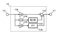
- FIG. 3 is a block diagram of the voltage control calculation unit 113.
- the same reference numerals are given to the same portions as those in FIG. 2, and the description thereof will be omitted as appropriate.
- the voltage control calculation unit 113 includes a proportional element composed of an amplifier 113A, an integral element composed of an amplifier 113B and an integrator 113C, a differential element composed of an amplifier 113D and a BPF 113E, and an adder 113F according to the present invention. It is a processor which is an example of “calculation means”. In the voltage control calculation unit 113, the proportional term (P term), the integral term (I term), and the differential term (D term) are calculated by these elements, and the calculated control terms are added by the adder 113F. Finally, the PID control amount corresponding to the current command value IR described above is calculated.
- the amplifier 113A is an amplifier related to the calculation of the P term of the PID control amount, and is configured to amplify the above-described VH deviation output from the adder / subtractor 112 according to a predetermined proportional gain kpv and send it to the adder 113F. It has become.
- the amplifier 113B is an amplifier related to the calculation of the I term in the PID control amount, and is configured to amplify the above-described VH deviation sent from the adder / subtractor 112 according to a predetermined integral gain kiv and send it to the integrator 113C. It has become.
- the integrator 113C integrates the VH deviation sent from the amplifier 113B and multiplied by the integration gain kiv, and then sends it to the adder 113F.
- the amplifier 113C is an amplifier related to the calculation of the D term of the PID control amount, and is configured to amplify the above-described VH deviation sent from the adder / subtractor 112 according to a predetermined differential gain kdv and send it to the BPF 113E. ing. In the BPF 113E, the VH deviation sent from the amplifier 113C multiplied by the differential gain kdv passes according to the band pass characteristic, and then sent to the adder 113F.
- the PID control amounts of the P term, the I term, and the D term supplied from the amplifier 113A, the integrator 113C, and the BPF 113E are added and processed as a current command value IR that is an output value of the voltage control calculation unit 113.
- the data is output to the adder / subtractor 117.
- the voltage control calculation unit 113 is configured as described above.
- FIG. 4 is a block diagram of the current control calculation unit 118.
- the same reference numerals are given to the same portions as those in FIG. 2, and the description thereof will be omitted as appropriate.
- a current control calculation unit 118 is a processor including a proportional element composed of an amplifier 118A, an integral element composed of an amplifier 118B and an integrator 118C, and an adder 118D.
- the proportional term (P term) and the integral term (I term) are calculated by each of these elements, and the calculated control terms are added by the adder 118D, and finally the duty described above.
- the PI control amount corresponding to d is calculated.
- the amplifier 118A is an amplifier related to the calculation of the P term in the PI control amount, and is configured to amplify the current deviation output from the adder / subtractor 117 according to a predetermined proportional gain kpi and send the amplified current deviation to the adder 118D. It has become.
- the amplifier 118B is an amplifier related to the calculation of the I term of the PI control amount, and is configured to amplify the above-described current deviation sent from the adder / subtractor 117 according to a predetermined integral gain kii and send it to the integrator 118C. It has become.
- the integrator 118C integrates the current deviation sent from the amplifier 118B and multiplied by the integration gain kii, and then sends it to the adder 118D.
- the current control calculation unit 118 is configured as described above.
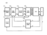
- FIG. 5 is a block diagram of the inverter control unit 120.
- the same reference numerals are given to the same portions as those in the above-described drawings, and the description thereof will be omitted as appropriate.
- the inverter control unit 120 includes a current command conversion unit 121, a current control unit 122, a two-phase / three-phase conversion unit 123, a three-phase / two-phase conversion unit 124, a carrier generation unit 114 (the boost converter control unit 110 and And a PWM converter 125.
- the current command conversion unit 121 generates a two-phase current command value (Idtg, Iqtg) based on the torque command value TR of the three-phase AC motor M1.
- the v-phase current Iv and the w-phase current Iw are supplied to the three-phase / two-phase converter 124 as feedback information.
- the three-phase current value is converted from the v-phase current Iv and the w-phase current Iw into a two-phase current value composed of the d-axis current Id and the q-axis current Iq.
- the converted two-phase current value is sent to the current control unit 122.
- the current control unit 122 based on the difference between the two-phase current command value generated in the current command conversion unit 121 and the two-phase current values Id and Iq received from the three-phase / two-phase conversion unit 124, d A two-phase voltage command value composed of the shaft voltage Vd and the q-axis voltage is generated. The generated two-phase voltage command values Vd and Vqh are sent to the two-phase / three-phase converter 123.
- the two-phase voltage command values Vd and Vq are converted into the three-phase voltage command values Vu, Vv and Vw.
- the converted three-phase voltage command values Vu, Vv, and Vw are sent to the PWM conversion unit 125.
- the PWM conversion unit 125 is configured to receive a carrier Car having a predetermined carrier frequency fcar from the carrier generation unit 114, and the carrier Car and the converted three-phase voltage command values Vu, Vv, and Vw. And the u-layer switching signals Gup and Gun, the v-phase switching signals Gvp and Gvn, and the w-phase switching signals Gwp and Gwn are generated in the inverter 300 by changing the logic state according to the comparison result. Supply.
- the signal with the identifier “p” is added to drive the p-side switching elements (Q3, Q5 and Q7) among the switching elements of each phase.
- the signal having the identifier “n” added thereto means a drive signal for driving the n-side switching elements (Q4, Q6, and Q8) among the switching elements of the respective phases.
- a switching signal for turning on the p-side switching element is generated.
- a switching signal for turning on the n-side switching element is generated. That is, the switching signal is a signal that is turned on and off, and one of the p-side and n-side switching elements is always on and the other is off.
- inverter 300 When inverter 300 is changed or maintained in the driving state of each switching element defined by each phase switching signal, three-phase AC motor M1 is driven according to the circuit state corresponding to the changed or maintained driving state. It has a configuration.
- Such a control mode of the inverter 300 is a so-called PWM control mode.
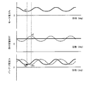
- FIG. 6 illustrates the phase relationship between the motor power Pm, which is the output power of the three-phase AC motor M1, the terminal voltage VH, which is the voltage across the smoothing capacitor C, and the battery current Ib, which is the output current of the battery B.
- the broken lines relating to the phase characteristics of the inter-terminal voltage VH and the battery current Ib indicate characteristics when the voltage control calculation unit 113 executes PI control instead of PID control.
- the PI control is affected by a 90 ° phase delay in the smoothing capacitor C before the influence appears in the inter-terminal voltage VH. Therefore, the influence of the white circle p1 appears in the inter-terminal voltage VH as the white circle p2 shown in the figure.
- the battery current Ib determined by feeding back the inter-terminal voltage VH is also affected by the phase delay in the smoothing capacitor C, and changes in a phase opposite to the inter-terminal voltage VH as shown by a white circle p3 shown on the broken line.
- the waveform of the battery current Ib does not match the actual waveform of the motor power Pm, and fluctuations in the inter-terminal voltage VH corresponding to the motor electrical frequency fmt cannot be suppressed.
- the withstand voltage of each of the switching elements of the smoothing capacitor C and the inverter 300 is at least as much as the fluctuation width of the inter-terminal voltage VH, and an increase in cost and size is inevitable.
- the phase of the battery current Ib and the phase of the motor power Pm can be matched on the time axis by the phase advance characteristic of the differential element. This is shown by the solid line.
- the battery current Ib takes the value of the illustrated black circle p4 with respect to the power point of the illustrated white circle p1.
- the waveform of the inter-terminal voltage VH is ideally a waveform having no voltage fluctuation corresponding to the motor electrical frequency, as shown by the solid line in the figure.
- the motor electrical frequency fmt is a value obtained by multiplying the reciprocal of the motor rotational speed per second by the number of magnetic pole pairs of the three-phase AC motor M1, for example, in the case of a three-phase AC motor having four magnetic pole pairs.
- FIG. 7 is a schematic Bode diagram conceptually showing the characteristics of the BPF 113E.
- the upper part represents the frequency characteristic of the passing signal level of the differential element in the voltage control calculation unit 113, and the lower part represents the frequency characteristic of the phase.
- a thick broken line in the figure is a characteristic when a general differentiator is employed as a differentiating element, and is a comparative example to be used for comparison with the present embodiment.
- the phase of the passing signal advances by 90 ° without depending on the frequency of the input signal. Therefore, a differentiator is useful as a differential element in terms of phase.
- the passing signal level of the differentiator increases linearly on the Bode diagram with respect to the frequency of the input signal. Therefore, the D term in the PID control is greatly influenced by the signal on the high frequency side when the inter-terminal voltage VH includes a signal having a frequency higher than the motor electrical frequency.
- the carrier frequency fcar of the carrier Car supplied from the carrier generation unit 114 described above is higher than the motor electrical frequency fmt, and the switching frequency of each switching element constituting the inverter 300 is approximately several k to several tens of kHz. It belongs to the high frequency region. Therefore, when a differentiator is used as the differentiating element, the differentiator tries to follow the voltage fluctuation corresponding to the switching frequency of the inverter 300 rather than the voltage fluctuation corresponding to the motor electric frequency. In addition to not being able to effectively suppress voltage fluctuations, the voltage VH between terminals of the smoothing capacitor C may become unstable.
- the pass signal level almost coincides with the case of the differentiator on the lower frequency side than the cut-off frequency fc indicated by the chain line in the figure, and the pass signal level is higher on the higher frequency side than the cut-off frequency fc. Attenuates due to the bandpass effect of the BPF.
- a phase advance characteristic almost identical to that of the differentiator is observed on the lower frequency side than the cut-off frequency fc, and in particular, the phase advance amount is 90 ° on the lower frequency side. Asymptotically.
- the BPF 113E has substantially the same effect as the differentiator.
- the differential element does not act on the voltage fluctuation corresponding to the switching frequency of the inverter 300 unlike the differentiator due to the signal attenuation action on the higher frequency side than the cutoff frequency fc. For this reason, voltage fluctuations corresponding to the motor electrical frequency can be selectively and reliably suppressed.
- the phase advance amount of the passing signal is zero at the cutoff frequency fc, and the passing signal is delayed from the input signal on the higher frequency side than the cutoff frequency fc.
- the frequency band that can be taken by the motor electrical frequency fmt is the illustrated band FBmtr (see hatching region) and the frequency band that can be used by the switching frequency of the inverter 300 is the illustrated band FBinv (hatching region)
- the cut-off frequency fc is accurately set, the region in which the phase advance amount decreases and the region in which the phase delay is subsequently generated do not overlap with the band FBmtr.
- the cut-off frequency fc of the BPF 113E is the middle of these two bands on the Bode diagram (on the higher frequency side than the upper limit value of the range that the motor electrical frequency fmt can actually take, and the inverter 300 It is located on the lower frequency side than the lower limit of the range that the switching frequency can actually take (in short, the carrier frequency fcar), and in the band FBmtr, the voltage fluctuation corresponding to the motor electrical frequency in the smoothing capacitor C is approximately.
- the setting mode of the cut-off frequency fc has a relatively large allowable range, for example, (90 ⁇ ) ° ( ⁇ in the illustrated band FBmtr corresponding to the motor electrical frequency.
- the signal is surely attenuated in the illustrated band FBinv corresponding to the switching frequency of the inverter 300 (for example, an attenuation of ⁇ 10 dB is ensured). It may be set on the lower frequency side than the cutoff frequency fc.
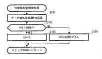
- FIG. 8 is a flowchart of the VH fluctuation suppression control process. This process is executed during the drive period of the motor drive system 10 in accordance with, for example, a control program stored in the ROM.
- the system configuration according to the second embodiment is equivalent to the motor drive system 10 according to the first embodiment.
- the control device 100 calculates the motor electrical frequency fmt (step S101).
- the definition of the motor electrical frequency fmt is as described above.
- the control device 100 determines whether or not the calculated motor electrical frequency fmt is a value on the higher frequency side than the reference frequency fmtb (step S102).
- step S101 If the motor electrical frequency fmt is higher than the reference frequency fmtb (step S101: YES), the control device 100 sets the differential gain kdv in the BPF 113E to zero via the voltage control calculation unit 113 (step S101). S103). The state in which the differential gain kdv is zero is equivalent to the voltage control calculation unit 113 performing PI control instead of PID control.
- step S101 NO
- the control device 100 maintains the differential gain kdv at the common D gain (assuming that the gain is equivalent to that in the first embodiment).
- Step S104 When the gain setting is completed, the process returns to step S101.
- the VH fluctuation suppression control process is executed as described above.
- FIG. 9 is a drive characteristic diagram of the three-phase AC motor M1.
- the vertical axis and the horizontal axis represent the motor torque Tm and the motor rotation speed Nm, respectively.
- the voltage fluctuation corresponding to the motor electrical frequency in the smoothing capacitor C depends on the motor electrical frequency fmt if only the frequency characteristic is seen, but the fluctuation range is also affected by the motor torque Tm. Specifically, the lower the motor torque Tm, the smaller the fluctuation range related to the voltage fluctuation.
- the reference frequency fmtb described above is a frequency corresponding to the reference motor rotation speed.
- the motor electrical frequency fmt is a value on the higher frequency side than the reference frequency fmtb that is determined in advance as a voltage fluctuation corresponding to the motor electrical frequency.
- the necessity for voltage fluctuation suppression is small, and the control mode of boost converter 200 is switched from PID control to PI control.
- the control mode of boost converter 200 is switched from PID control to PI control.
- the reference frequency fmtb is about 1/2 to 1/4 of the cut-off frequency fc from the viewpoint of securing a desirable phase advance characteristic. Is desirable. Therefore, in the case where the reference motor rotation speed is determined in advance, after the reference frequency fmtb is determined as the motor electrical frequency corresponding to the reference motor rotation speed, the frequency value is about 2 to 4 times the fmtb. As a result, the cutoff frequency fc of the BPF 113E can be determined.
- the present invention is not limited to the above-described embodiment, and can be appropriately changed without departing from the spirit or idea of the invention that can be read from the claims and the entire specification, and control of the boost converter accompanying such a change.
- the apparatus is also included in the technical scope of the present invention.
- the present invention can be applied to control of a boost converter in AC motor drive control.
- SYMBOLS 10 Motor drive system, 100 ... Control apparatus, 110 ... Boost converter control part, 113 ... Voltage control calculating part, 113E ... BPF (bandpass filter), 120 ... Inverter control part, 200 ... Boost converter, 300 ... Inverter, C ... smoothing capacitor, B ... DC power supply, M1 ... three-phase AC motor.
Abstract
Description
以下、図面を参照して、本発明の好適な各種実施形態について説明する。 <Embodiment of the Invention>
Various preferred embodiments of the present invention will be described below with reference to the drawings.
<実施形態の構成>
始めに、図1を参照し、本実施形態に係るモータ駆動システム10の構成について説明する。ここに、図1は、モータ駆動システム10の構成を概念的に表すシステム構成図である。 <First Embodiment>
<Configuration of Embodiment>
First, the configuration of the
<電圧制御演算部113におけるPID制御の効果>
次に、図6を参照し、本実施形態の効果として、PID制御の効果について説明する。ここに、図6は、三相交流モータM1の出力電力たるモータ電力Pm、平滑コンデンサCの端子間電圧である端子間電圧VH及びバッテリBの出力電流であるバッテリ電流Ibの位相関係を説明する図である。 <Effect of embodiment>
<Effect of PID Control in Voltage
Next, the effect of PID control will be described as an effect of this embodiment with reference to FIG. FIG. 6 illustrates the phase relationship between the motor power Pm, which is the output power of the three-phase AC motor M1, the terminal voltage VH, which is the voltage across the smoothing capacitor C, and the battery current Ib, which is the output current of the battery B. FIG.
次に、図7を参照し、本実施形態の効果として、BPF113Eの効果について説明する。ここに、図7は、BPF113Eの特性を概念的に表す模式的なボード線図である。 <Effect of BPF in Voltage
Next, with reference to FIG. 7, the effect of BPF113E is demonstrated as an effect of this embodiment. FIG. 7 is a schematic Bode diagram conceptually showing the characteristics of the BPF 113E.
次に、図8を参照し、本発明の第2実施形態として、制御装置100により実行されるVH変動抑制制御処理について説明する。ここに、図8は、VH変動抑制制御処理のフローチャートである。尚、この処理は、例えばROMに格納される制御プログラムに従って、モータ駆動システム10の駆動期間において実行される。尚、第2実施形態に係るシステム構成は、第1実施形態に係るモータ駆動システム10と同等であるとする。 Second Embodiment
Next, a VH fluctuation suppression control process executed by the
Claims (4)
- 直流電源と、
三相交流モータと、
前記直流電源と前記三相交流モータとの間に設けられ、前記三相交流モータの三相各々に対応するスイッチング回路及び該スイッチング回路に対し電気的に並列に配置された平滑コンデンサを含んでなる電力変換器と、
前記電力変換器と前記直流電源との間に設置され、前記直流電源の直流電圧を昇圧して前記電力変換器に供給する昇圧コンバータと
を備えたモータ駆動システムにおいて前記昇圧コンバータを制御する昇圧コンバータの制御装置であって、
比例要素、積分要素及び微分要素を備え、且つ該微分要素が帯域通過フィルタとして構成されると共に、前記昇圧コンバータの出力電圧を前記平滑コンデンサの端子間電圧VHの指令値に維持するための前記昇圧コンバータの電流指令値に相当するPID制御量を演算する演算手段と、
前記演算されたPID制御量に基づいて前記昇圧コンバータの出力電圧を制御する制御手段と
を具備することを特徴とする昇圧コンバータの制御装置。 DC power supply,
A three-phase AC motor,
A switching circuit provided between the DC power supply and the three-phase AC motor and corresponding to each of the three phases of the three-phase AC motor; and a smoothing capacitor disposed in parallel with the switching circuit. A power converter;
A boost converter that is installed between the power converter and the DC power supply, and that boosts a DC voltage of the DC power supply and supplies the boosted converter to the power converter. A control device of
The booster includes a proportional element, an integral element, and a differential element, and the differential element is configured as a band pass filter, and maintains the output voltage of the boost converter at a command value of the terminal voltage VH of the smoothing capacitor. Computing means for computing a PID control amount corresponding to the current command value of the converter;
And a control means for controlling the output voltage of the boost converter based on the calculated PID control amount. - 前記昇圧コンバータは、
前記直流電源の正極に一端が接続されるリアクトルと、
前記リアクトルの他端と前記電力変換器との間に接続される第1スイッチング素子と、
前記リアクトルの他端と前記直流電源の負極との間に接続される第2スイッチング素子と、
前記第1及び第2スイッチング素子に夫々逆並列に接続される第1及び第2ダイオードと
を含む
ことを特徴とする請求の範囲第1項に記載の昇圧コンバータの制御装置。 The boost converter includes:
A reactor having one end connected to the positive electrode of the DC power supply;
A first switching element connected between the other end of the reactor and the power converter;
A second switching element connected between the other end of the reactor and the negative electrode of the DC power source;
2. The boost converter control device according to claim 1, comprising: first and second diodes connected in antiparallel to the first and second switching elements, respectively. 3. - 前記帯域通過フィルタのカットオフ周波数は、前記三相交流モータの回転速度に比例するモータ電気周波数の上限値以上、且つ前記電力変換器のキャリア周波数の下限値未満である
ことを特徴とする請求の範囲第1項に記載の昇圧コンバータの制御装置。 The cut-off frequency of the band-pass filter is not less than an upper limit value of a motor electrical frequency proportional to a rotation speed of the three-phase AC motor and less than a lower limit value of a carrier frequency of the power converter. The control device for a boost converter according to claim 1 in the range. - 前記演算手段は、前記三相交流モータの回転速度が所定値以上である場合に、前記PID制御量に替えて、前記微分要素が無効となるPI制御量を演算し、
前記制御手段は、前記演算されたPI制御量に基づいて前記出力電圧を制御する
ことを特徴とする請求の範囲第1項に記載の昇圧コンバータの制御装置。 When the rotational speed of the three-phase AC motor is equal to or higher than a predetermined value, the calculation means calculates a PI control amount that makes the differential element invalid, instead of the PID control amount,
2. The boost converter control device according to claim 1, wherein the control unit controls the output voltage based on the calculated PI control amount. 3.
Priority Applications (6)
| Application Number | Priority Date | Filing Date | Title |
|---|---|---|---|
| JP2013510769A JP5637303B2 (en) | 2011-04-19 | 2011-04-19 | Boost converter controller |
| PCT/JP2011/059651 WO2012144018A1 (en) | 2011-04-19 | 2011-04-19 | Boost converter control device |
| EP11863860.0A EP2701296B1 (en) | 2011-04-19 | 2011-04-19 | Boost converter control device |
| CN201180070281.2A CN103477546B (en) | 2011-04-19 | 2011-04-19 | The control device of booster converter |
| EP16160998.7A EP3051678B1 (en) | 2011-04-19 | 2011-04-19 | Boost converter control apparatus |
| US14/112,139 US9035594B2 (en) | 2011-04-19 | 2011-04-19 | Boost converter control apparatus |
Applications Claiming Priority (1)
| Application Number | Priority Date | Filing Date | Title |
|---|---|---|---|
| PCT/JP2011/059651 WO2012144018A1 (en) | 2011-04-19 | 2011-04-19 | Boost converter control device |
Publications (1)
| Publication Number | Publication Date |
|---|---|
| WO2012144018A1 true WO2012144018A1 (en) | 2012-10-26 |
Family
ID=47041168
Family Applications (1)
| Application Number | Title | Priority Date | Filing Date |
|---|---|---|---|
| PCT/JP2011/059651 WO2012144018A1 (en) | 2011-04-19 | 2011-04-19 | Boost converter control device |
Country Status (5)
| Country | Link |
|---|---|
| US (1) | US9035594B2 (en) |
| EP (2) | EP3051678B1 (en) |
| JP (1) | JP5637303B2 (en) |
| CN (1) | CN103477546B (en) |
| WO (1) | WO2012144018A1 (en) |
Cited By (4)
| Publication number | Priority date | Publication date | Assignee | Title |
|---|---|---|---|---|
| CN105811848A (en) * | 2016-03-21 | 2016-07-27 | 太原理工大学 | Proportional integral (PI) control method for variable gain of switched reluctance motor |
| JP2021516531A (en) * | 2018-03-19 | 2021-07-01 | トゥラ イーテクノロジー,インコーポレイテッド | Pulsed electromechanical control |
| JP7187818B2 (en) | 2018-05-22 | 2022-12-13 | 株式会社デンソー | Rotating electric machine control device |
| JP7371175B2 (en) | 2017-03-10 | 2023-10-30 | ローム株式会社 | DC/DC converter |
Families Citing this family (18)
| Publication number | Priority date | Publication date | Assignee | Title |
|---|---|---|---|---|
| US20130076128A1 (en) * | 2011-09-28 | 2013-03-28 | Caterpillar, Inc. | Active Switching Frequency Modulation |
| US9003216B2 (en) | 2011-10-03 | 2015-04-07 | Microsoft Technology Licensing, Llc | Power regulation of power grid via datacenter |
| JP6248596B2 (en) * | 2013-12-10 | 2017-12-20 | トヨタ自動車株式会社 | Motor controller for hybrid vehicle |
| JP6007939B2 (en) * | 2014-04-23 | 2016-10-19 | 株式会社デンソー | Switching control device |
| KR101575294B1 (en) * | 2014-06-02 | 2015-12-21 | 현대자동차 주식회사 | Method of estimating voltage of input terminal of inverter and method of controlling motor using the same |
| CN105391286B (en) * | 2015-11-06 | 2018-05-01 | 上海斐讯数据通信技术有限公司 | A kind of power-supplying circuit based on high-pass platform |
| US10944352B2 (en) | 2018-03-19 | 2021-03-09 | Tula eTechnology, Inc. | Boosted converter for pulsed electric machine control |
| US11623529B2 (en) | 2018-03-19 | 2023-04-11 | Tula eTechnology, Inc. | Pulse modulated control with field weakening for improved motor efficiency |
| JP6985222B2 (en) * | 2018-08-03 | 2021-12-22 | 日立Astemo株式会社 | Boost converter controller |
| US11011972B1 (en) * | 2019-11-18 | 2021-05-18 | Infineon Technologies Austria Ag | Frequency alignment and switch-over in power supplies |
| US11628730B2 (en) | 2021-01-26 | 2023-04-18 | Tula eTechnology, Inc. | Pulsed electric machine control |
| EP4308405A1 (en) | 2021-03-15 | 2024-01-24 | TULA eTechnology, Inc. | Methods of optimizing waveforms for electric motors |
| US11695361B2 (en) | 2021-06-14 | 2023-07-04 | Tula eTechnology, Inc. | Electric machines with efficient torque transitions |
| US11557996B1 (en) | 2021-07-08 | 2023-01-17 | Tula eTechnology, Inc. | Methods of reducing vibrations for electric motors |
| US11345241B1 (en) | 2021-08-12 | 2022-05-31 | Tula eTechnology, Inc. | Method of optimizing system efficiency for battery powered electric motors |
| US11916498B2 (en) | 2021-09-08 | 2024-02-27 | Tule eTechnology Inc. | Electric machine torque adjustment based on waveform integer multiples |
| US11637466B1 (en) | 2021-10-18 | 2023-04-25 | Tula Etechnology Inc. | Mechanical and electromechanical arrangements for field-weakening of an electric machine that utilizes permanent magnets |
| US11888424B1 (en) | 2022-07-18 | 2024-01-30 | Tula eTechnology, Inc. | Methods for improving rate of rise of torque in electric machines with stator current biasing |
Citations (4)
| Publication number | Priority date | Publication date | Assignee | Title |
|---|---|---|---|---|
| JPH0914265A (en) * | 1995-06-27 | 1997-01-14 | Shinko Electric Co Ltd | Magnetic bearing compensating circuit |
| JP2004112904A (en) | 2002-09-18 | 2004-04-08 | Toyota Motor Corp | Voltage converter, voltage conversion method, and computer-readable recording medium with program for making computer control voltage conversion recorded thereon |
| JP2006254518A (en) * | 2005-03-08 | 2006-09-21 | Yaskawa Electric Corp | Chopper device and control method for the same |
| JP2010200534A (en) * | 2009-02-26 | 2010-09-09 | Toyota Motor Corp | Voltage conversion device |
Family Cites Families (3)
| Publication number | Priority date | Publication date | Assignee | Title |
|---|---|---|---|---|
| JP2002171778A (en) * | 2000-09-25 | 2002-06-14 | Aisin Seiki Co Ltd | Device for suppressing and controlling vibrations of electric motor and designing technique in suppression and control of the vibrations of the electric motor |
| CN100406708C (en) * | 2003-07-02 | 2008-07-30 | 蒂艾克思股份有限公司 | Free piston stirling engine control |
| JP4052195B2 (en) * | 2003-07-31 | 2008-02-27 | トヨタ自動車株式会社 | Voltage conversion device and computer-readable recording medium recording program for causing computer to execute control of voltage conversion |
-
2011
- 2011-04-19 EP EP16160998.7A patent/EP3051678B1/en active Active
- 2011-04-19 EP EP11863860.0A patent/EP2701296B1/en active Active
- 2011-04-19 WO PCT/JP2011/059651 patent/WO2012144018A1/en active Application Filing
- 2011-04-19 JP JP2013510769A patent/JP5637303B2/en active Active
- 2011-04-19 CN CN201180070281.2A patent/CN103477546B/en active Active
- 2011-04-19 US US14/112,139 patent/US9035594B2/en active Active
Patent Citations (4)
| Publication number | Priority date | Publication date | Assignee | Title |
|---|---|---|---|---|
| JPH0914265A (en) * | 1995-06-27 | 1997-01-14 | Shinko Electric Co Ltd | Magnetic bearing compensating circuit |
| JP2004112904A (en) | 2002-09-18 | 2004-04-08 | Toyota Motor Corp | Voltage converter, voltage conversion method, and computer-readable recording medium with program for making computer control voltage conversion recorded thereon |
| JP2006254518A (en) * | 2005-03-08 | 2006-09-21 | Yaskawa Electric Corp | Chopper device and control method for the same |
| JP2010200534A (en) * | 2009-02-26 | 2010-09-09 | Toyota Motor Corp | Voltage conversion device |
Cited By (5)
| Publication number | Priority date | Publication date | Assignee | Title |
|---|---|---|---|---|
| CN105811848A (en) * | 2016-03-21 | 2016-07-27 | 太原理工大学 | Proportional integral (PI) control method for variable gain of switched reluctance motor |
| JP7371175B2 (en) | 2017-03-10 | 2023-10-30 | ローム株式会社 | DC/DC converter |
| JP2021516531A (en) * | 2018-03-19 | 2021-07-01 | トゥラ イーテクノロジー,インコーポレイテッド | Pulsed electromechanical control |
| JP7082679B2 (en) | 2018-03-19 | 2022-06-08 | トゥラ イーテクノロジー,インコーポレイテッド | Pulsed electromechanical control |
| JP7187818B2 (en) | 2018-05-22 | 2022-12-13 | 株式会社デンソー | Rotating electric machine control device |
Also Published As
| Publication number | Publication date |
|---|---|
| US9035594B2 (en) | 2015-05-19 |
| EP3051678B1 (en) | 2017-07-05 |
| JP5637303B2 (en) | 2014-12-10 |
| EP3051678A1 (en) | 2016-08-03 |
| JPWO2012144018A1 (en) | 2014-07-28 |
| CN103477546A (en) | 2013-12-25 |
| US20140028225A1 (en) | 2014-01-30 |
| EP2701296A1 (en) | 2014-02-26 |
| CN103477546B (en) | 2016-04-20 |
| EP2701296A4 (en) | 2015-11-18 |
| EP2701296B1 (en) | 2019-07-24 |
Similar Documents
| Publication | Publication Date | Title |
|---|---|---|
| JP5637303B2 (en) | Boost converter controller | |
| JP5429403B2 (en) | Boost converter controller | |
| JP4706324B2 (en) | Control device for motor drive system | |
| JP4353304B2 (en) | Motor drive control device | |
| JP5472475B2 (en) | Control device for motor drive system | |
| JP5910752B2 (en) | Boost converter controller | |
| WO2010137128A1 (en) | Converter control device and electric vehicle using the same | |
| JP2010161907A (en) | Controller for motor driving control system | |
| US10224857B2 (en) | Motor controller | |
| JP2010119268A (en) | Apparatus and method for detecting fault of inverter | |
| JP2018186684A (en) | Automobile | |
| JP6852539B2 (en) | Rotating machine control device | |
| JP5210822B2 (en) | AC motor control device and electric vehicle equipped with the same | |
| JP5407553B2 (en) | Motor control device | |
| JP7415579B2 (en) | Vehicle drive control system | |
| JP2015201937A (en) | voltage conversion device | |
| JP2010124662A (en) | Motor drive system | |
| JP6221824B2 (en) | Control device for power converter | |
| JP5686110B2 (en) | Control device for AC electric machine drive system | |
| JP2015202018A (en) | voltage conversion device | |
| JP2010166707A (en) | Controller of ac motor | |
| JP2014099949A (en) | Step-up converter controller | |
| JP2008211926A (en) | Power converter and its control method |
Legal Events
| Date | Code | Title | Description |
|---|---|---|---|
| WWE | Wipo information: entry into national phase |
Ref document number: 201180070281.2 Country of ref document: CN |
|
| 121 | Ep: the epo has been informed by wipo that ep was designated in this application |
Ref document number: 11863860 Country of ref document: EP Kind code of ref document: A1 |
|
| WWE | Wipo information: entry into national phase |
Ref document number: 14112139 Country of ref document: US Ref document number: 2011863860 Country of ref document: EP |
|
| ENP | Entry into the national phase |
Ref document number: 2013510769 Country of ref document: JP Kind code of ref document: A |
|
| NENP | Non-entry into the national phase |
Ref country code: DE |