WO2012127573A1 - 光論理素子 - Google Patents
光論理素子 Download PDFInfo
- Publication number
- WO2012127573A1 WO2012127573A1 PCT/JP2011/056596 JP2011056596W WO2012127573A1 WO 2012127573 A1 WO2012127573 A1 WO 2012127573A1 JP 2011056596 W JP2011056596 W JP 2011056596W WO 2012127573 A1 WO2012127573 A1 WO 2012127573A1
- Authority
- WO
- WIPO (PCT)
- Prior art keywords
- quantum dot
- quantum dots
- optical logic
- quantum
- distance
- Prior art date
- Legal status (The legal status is an assumption and is not a legal conclusion. Google has not performed a legal analysis and makes no representation as to the accuracy of the status listed.)
- Ceased
Links
Images



Classifications
-
- G—PHYSICS
- G02—OPTICS
- G02F—OPTICAL DEVICES OR ARRANGEMENTS FOR THE CONTROL OF LIGHT BY MODIFICATION OF THE OPTICAL PROPERTIES OF THE MEDIA OF THE ELEMENTS INVOLVED THEREIN; NON-LINEAR OPTICS; FREQUENCY-CHANGING OF LIGHT; OPTICAL LOGIC ELEMENTS; OPTICAL ANALOGUE/DIGITAL CONVERTERS
- G02F3/00—Optical logic elements; Optical bistable devices
- G02F3/02—Optical bistable devices
-
- B—PERFORMING OPERATIONS; TRANSPORTING
- B82—NANOTECHNOLOGY
- B82Y—SPECIFIC USES OR APPLICATIONS OF NANOSTRUCTURES; MEASUREMENT OR ANALYSIS OF NANOSTRUCTURES; MANUFACTURE OR TREATMENT OF NANOSTRUCTURES
- B82Y20/00—Nanooptics, e.g. quantum optics or photonic crystals
-
- G—PHYSICS
- G02—OPTICS
- G02F—OPTICAL DEVICES OR ARRANGEMENTS FOR THE CONTROL OF LIGHT BY MODIFICATION OF THE OPTICAL PROPERTIES OF THE MEDIA OF THE ELEMENTS INVOLVED THEREIN; NON-LINEAR OPTICS; FREQUENCY-CHANGING OF LIGHT; OPTICAL LOGIC ELEMENTS; OPTICAL ANALOGUE/DIGITAL CONVERTERS
- G02F1/00—Devices or arrangements for the control of the intensity, colour, phase, polarisation or direction of light arriving from an independent light source, e.g. switching, gating or modulating; Non-linear optics
- G02F1/01—Devices or arrangements for the control of the intensity, colour, phase, polarisation or direction of light arriving from an independent light source, e.g. switching, gating or modulating; Non-linear optics for the control of the intensity, phase, polarisation or colour
- G02F1/015—Devices or arrangements for the control of the intensity, colour, phase, polarisation or direction of light arriving from an independent light source, e.g. switching, gating or modulating; Non-linear optics for the control of the intensity, phase, polarisation or colour based on semiconductor elements having potential barriers, e.g. having a PN or PIN junction
- G02F1/017—Structures with periodic or quasi periodic potential variation, e.g. superlattices, quantum wells
-
- G—PHYSICS
- G02—OPTICS
- G02F—OPTICAL DEVICES OR ARRANGEMENTS FOR THE CONTROL OF LIGHT BY MODIFICATION OF THE OPTICAL PROPERTIES OF THE MEDIA OF THE ELEMENTS INVOLVED THEREIN; NON-LINEAR OPTICS; FREQUENCY-CHANGING OF LIGHT; OPTICAL LOGIC ELEMENTS; OPTICAL ANALOGUE/DIGITAL CONVERTERS
- G02F1/00—Devices or arrangements for the control of the intensity, colour, phase, polarisation or direction of light arriving from an independent light source, e.g. switching, gating or modulating; Non-linear optics
- G02F1/01—Devices or arrangements for the control of the intensity, colour, phase, polarisation or direction of light arriving from an independent light source, e.g. switching, gating or modulating; Non-linear optics for the control of the intensity, phase, polarisation or colour
- G02F1/015—Devices or arrangements for the control of the intensity, colour, phase, polarisation or direction of light arriving from an independent light source, e.g. switching, gating or modulating; Non-linear optics for the control of the intensity, phase, polarisation or colour based on semiconductor elements having potential barriers, e.g. having a PN or PIN junction
- G02F1/017—Structures with periodic or quasi periodic potential variation, e.g. superlattices, quantum wells
- G02F1/01791—Quantum boxes or quantum dots
-
- G—PHYSICS
- G02—OPTICS
- G02F—OPTICAL DEVICES OR ARRANGEMENTS FOR THE CONTROL OF LIGHT BY MODIFICATION OF THE OPTICAL PROPERTIES OF THE MEDIA OF THE ELEMENTS INVOLVED THEREIN; NON-LINEAR OPTICS; FREQUENCY-CHANGING OF LIGHT; OPTICAL LOGIC ELEMENTS; OPTICAL ANALOGUE/DIGITAL CONVERTERS
- G02F2202/00—Materials and properties
- G02F2202/10—Materials and properties semiconductor
- G02F2202/101—Ga×As and alloy
Definitions
- the present invention relates to the technical field of optical logic elements that perform optical logic operations using, for example, near-field light or propagating light.
- an element including a first quantum point, a second quantum point, and a third quantum point in order of increasing size is proposed.
- the adjustment signal energy is input to the third quantum point.
- the energy forbidden to move to the third quantum point is output from the second quantum point as signal energy (see Patent Document 1).
- the present invention has been made in view of the above problems, for example, and an object thereof is to provide an optical logic element capable of performing a stable logic operation.
- an optical logic element of the present invention includes a substrate, and first and second quantum dots that are arranged on the substrate and can transfer energy by near-field interaction,
- the distance between the first quantum dot and the second quantum dot is 13 nm (nanometer) to 26 nm.
- the first quantum dots and the second quantum dots including, for example, indium arsenic (InAs) are disposed on the substrate including, for example, gallium arsenide (GaAs).
- the first quantum dots and the second quantum dots may be arranged on a plane parallel to the substrate surface, or along a direction perpendicular to the substrate surface (that is, a height direction), They may be arranged (laminated) at different distances from the substrate surface.
- the optical logic element is not limited to the first quantum dot and the second quantum dot, and may include three or more quantum dots. That is, in the present invention, among the plurality of quantum dots, one quantum dot is referred to as a “first quantum dot”, and another quantum dot disposed in proximity to the one quantum dot is referred to as a “second quantum dot”. For convenience.
- the first quantum dots and the second quantum dots are arranged so that the distance between the first quantum dots and the second quantum dots is within a range of 13 nm to 26 nm.
- the “distance between the first quantum dot and the second quantum dot” is the shortest distance between the outer edge (ie, the surface) of the first quantum dot and the outer edge (ie, the surface) of the second quantum dot. Means distance.
- the following matters have been found. That is, if the distance between the first quantum dot and the second quantum dot is relatively long, the near-field interaction does not work between the first quantum dot and the second quantum dot, and no logic operation is performed in the optical logic element. There is a fear. On the other hand, if the distance between the first quantum dots and the second quantum dots is relatively short, there is a possibility that light (that is, energy) is not appropriately emitted from the quantum dots.
- the present inventor uses a plurality of samples in which the distance between the first quantum dot and the second quantum dot is different from each other, and an appropriate range of the distance between the first quantum dot and the second quantum dot is 13 nm to It was experimentally found to be 26 nm.
- the range is not affected or hardly affected by the size of the quantum dots.
- the distance between the first quantum dots and the second quantum dots is set to 13 nm to 26 nm. Therefore, according to the present invention, it is possible to provide an optical logic element that enables stable logic operation.
- the logical operation is performed by irradiating the optical logic element with light having a predetermined wavelength. Since various known modes can be applied to the logical operation, a detailed description thereof is omitted.
- the distance between the first quantum dots and the second quantum dots is 17 nm to 24 nm.
- the first quantum dot and the second quantum dot include a material different from a material constituting the first quantum dot and a material constituting the second quantum dot. Are stacked on the substrate so as to face each other with an intermediate layer formed therebetween.
- the first quantum dots and the second quantum dots are stacked so as to face each other with the intermediate layer interposed therebetween. That is, in this aspect, (i) an intermediate layer is stacked on the first quantum dot, and a second quantum dot is stacked on the intermediate layer, or (ii) on the second quantum dot An intermediate layer is stacked, and the first quantum dots are stacked on the intermediate layer. With this configuration, the installation area of the optical logic element can be reduced, which is very advantageous in practice.
- opposite means that one of the first quantum dots and the second quantum dots is arranged on one surface of the intermediate layer, and the other surface opposite to the one surface of the intermediate layer, It is only necessary that the other of the first quantum dots and the second quantum dots is arranged, and the present invention is not limited to the case where the first quantum dots and the second quantum dots are overlapped when viewed in plan on the substrate.
- FIG. 6 is a characteristic diagram showing a relationship between a distance d and a wavelength difference between the first level and the second level. It is an example of the quantum dot observed by HAADF-STEM. It is a conceptual diagram which shows an example of arrangement
- FIG. 1 is a conceptual diagram showing the configuration of the optical logic element of this embodiment.
- the optical logic device 1 includes a GaAs substrate 11, a GaAs buffer layer 12 stacked on the (001) plane of the GaAs substrate 11, and a stack on the GaAs buffer layer 12.
- the optical logic element 1 may be configured to include three or more quantum dot layers. Moreover, the material which comprises the optical logic element 1 is not restricted to the material mentioned above.
- the optical logic element 1 when the optical logic element 1 is irradiated with light having a predetermined wavelength from below the GaAs substrate 11 of the optical logic element 1, a near-field interaction works between the InAs quantum dots 21 and the InAs quantum dots 22 (specifically Specifically, for example, energy is exchanged via near-field light) and a predetermined logical operation is performed.
- the optical logic device 1 is configured such that the distance d (see FIG. 1) between the InAs quantum dots 21 and the InAs quantum dots 22 is 13 nm to 26 nm, preferably 17 nm to 24 nm. As shown in FIG. 1, the distance d means the distance between the outer edge of the InAs quantum dot 21 and the outer edge of the InAs quantum dot 22.
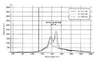
- FIG. 2 is an example of the relationship between the distance d and a PL (Photoluminescence) emission peak
- FIG. 3 is another example of the relationship between the distance d and the PL emission peak
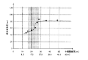
- FIG. 4 is a characteristic diagram showing the relationship between the distance d and the wavelength difference between the first level and the second level.
- the first level PL emission peak (peaks appearing at wavelengths 1230 nm to 1300 nm) becomes longer, so that the first level is increased. -It can be seen that the wavelength difference between the second levels increases.
- FIGS. 2 and 3 there is a PL emission peak in the vicinity of a wavelength of 1060 nm. This is a case where the laser beam irradiated for the measurement of the PL emission characteristic is detected as noise.
- FIG. 4 shows the relationship between the wavelength difference between the first level and the second level of the PL emission peak described above and the distance d.
- the distance d is 13 nm to 17 nm
- the wavelength difference between the first level and the second level gradually increases (that is, the wavelength of the PL emission peak mainly at the second level becomes longer).
- the distance d is 17 nm to 26 nm
- the wavelength difference between the first level and the second level rapidly increases.
- the distance d is 26 nm or more, there is no significant change in the wavelength difference between the first level and the second level.
- the near-field interaction As a result, it has been found that the wavelength of the PL emission peak at the second level mainly increases. For this reason, if the distance d between the InAs quantum dots 21 and the InAs quantum dots 22 is set so as to be within a section where the wavelength difference between the first level and the second level changes, the near-field interaction is stabilized. Will work. That is, the optical logic element 1 can be made to perform a stable logic operation.
- the optical logic element 1 can perform more stable logic operation. Is possible.
- HAADF-SREM High-Angle Angular Dark-Field Scanning Transmission Electron Microscopy: High Angle Scattering Dark Field Scanning Transmission Electron Microscopy.
- the InAs quantum dots included in the second quantum dot layer (upper layer) are formed immediately above the InAs quantum dots included in the first quantum dot layer (lower layer). I understand. This is because distortion caused by the InAs quantum dots 21 occurs on the surface (upper surface) of the intermediate layer 13 (see FIG. 1).
- the “InAs quantum dots 21” and “InAs quantum dots 22” according to the present embodiment are examples of the “first quantum dots” and the “second quantum dots” according to the present invention, respectively.
- the present invention is also applicable to an optical logic element including only one quantum dot layer, for example.
- the distance d between the InAs quantum dots 21 and InAs quantum dots 22 formed in the upper layer of the GaAs substrate 11 is within the above-mentioned range of 13 nm to 26 nm. Desirably, it may be set within a range of 17 nm to 24 nm.
- Optical logic element 11 ... GaAs substrate, 12 ... GaAs buffer layer, 13 ... intermediate layer, 14 ... cap layer, 21, 22 ... InAs quantum dots
Landscapes
- Physics & Mathematics (AREA)
- Nonlinear Science (AREA)
- Optics & Photonics (AREA)
- General Physics & Mathematics (AREA)
- Chemical & Material Sciences (AREA)
- Engineering & Computer Science (AREA)
- Nanotechnology (AREA)
- Life Sciences & Earth Sciences (AREA)
- Biophysics (AREA)
- Crystallography & Structural Chemistry (AREA)
- Semiconductor Lasers (AREA)
Abstract
光論理素子(1)は、基板(11)と、該基板上に配置され、近接場相互作用によりエネルギーを授受可能な第1量子ドット(21)及び第2量子ドット(22)と、を備える。ここで特に、第1量子ドット及び第2量子ドット間の距離は、13nm~26nmである。このように構成すれば、安定して論理動作が行われる光論理素子を提供することができる。
Description
本発明は、例えば近接場光或いは伝播光を用いて光論理動作を行う光論理素子の技術分野に関する。
この種の素子として、例えば、夫々大きさが異なる、小さい順に、第1の量子点、第2の量子点及び第3の量子点を備える素子が提案されている。ここでは特に、第1の量子点から第2の量子点へ、該第2の量子点から第3の量子点へ、エネルギー移動が生じる際に、第3の量子点に調整信号エネルギーが入力されると、第3の量子点への移動が禁制されたエネルギーが、信号エネルギーとして第2の量子点から出力されることが開示されている(特許文献1参照)。
特許文献1に記載されているような素子を用いて、例えば光論理素子を構成した場合、素子に含まれる量子ドットの配置によっては、適切に論理動作が行われない可能性があるという技術的問題点がある。
本発明は、例えば上記問題点に鑑みてなされたものであり、安定して論理動作が行われる光論理素子を提供することを課題とする。
本発明の光論理素子は、上記課題を解決するために、基板と、前記基板上に配置され、近接場相互作用によりエネルギーを授受可能な第1量子ドット及び第2量子ドットと、を備え、前記第1量子ドット及び前記第2量子ドット間の距離が、13nm(ナノメートル)~26nmである。
本発明の光論理素子によれば、例えばガリウムヒ素(GaAs)等を含んでなる基板上に、例えばインジウムヒ素(InAs)等を含んでなる第1量子ドット及び第2量子ドットが配置されている。ここで、第1量子ドット及び第2量子ドットは、基板面に平行な平面上に配置されていてもよいし、該基板面に対して垂直な方向(即ち、高さ方向)に沿って、基板面から互いに異なる距離に配置(積層)されていてもよい。
また、当該光論理素子は、第1量子ドット及び第2量子ドットに限らず、3つ以上の量子ドットを備えていてよい。つまり、本発明では、複数の量子ドットのうち、一の量子ドットを「第1量子ドット」と、該一の量子ドットに近接して配置されている他の量子ドットを「第2量子ドット」と、便宜上称している。
本発明では特に、第1量子ドット及び第2量子ドット間の距離が、13nm~26nmの範囲内になるように、該第1量子ドット及び第2量子ドットが配置されている。ここで、「第1量子ドット及び第2量子ドット間の距離」とは、第1量子ドットの外縁(即ち、表面)と、第2量子ドットの外縁(即ち、表面)と、の間の最短距離を意味する。
本願発明者の研究によれば、以下の事項が判明している。即ち、第1量子ドット及び第2量子ドット間の距離が、比較的長いと、第1量子ドット及び第2量子ドット間において近接場相互作用が働かず、光論理素子において論理動作が行われないおそれがある。他方、第1量子ドット及び第2量子ドット間の距離が、比較的短いと、量子ドットから適切に光(即ち、エネルギー)が発せられないおそれがある。
そこで、本願発明者は、第1量子ドット及び第2量子ドット間の距離が相互に異なる複数のサンプルを用いて、第1量子ドット及び第2量子ドット間の距離の適切な範囲が、13nm~26nmであることを実験的に見出した。ここで、該範囲は、量子ドットの大きさの影響を受けない又はほとんど受けないことが本願発明者の研究により判明している。
本発明の光論理素子は、上述の如く、第1量子ドット及び第2量子ドット間の距離が、13nm~26nmに設定されている。従って、本発明によれば、安定した論理動作を可能とする光論理素子を提供することができる。尚、論理動作は、当該光論理素子に対して、所定の波長を有する光が照射されることにより行われる。論理動作には、公知の各種態様を適用可能であるので、その詳細についての説明は省略する。
本発明の光論理素子の一態様では、前記第1量子ドット及び前記第2量子ドット間の距離が、17nm~24nmである。
この態様によれば、より安定した論理動作を可能とする光論理素子を提供することができ、実用上非常に有利である。
本発明の光論理素子の他の態様では、前記第1量子ドット及び前記第2量子ドットは、前記第1量子ドットを構成する材料及び前記第2量子ドットを構成する材料とは異なる材料を含んでなる中間層を挟んで相対向するように、前記基板上に積層されている。
この態様によれば、第1量子ドット及び第2量子ドットは、中間層を挟んで相対向するように積層されている。つまり、この態様では、(i)第1量子ドットの上に中間層が積層され、該中間層の上に第2量子ドットが積層されている、或いは、(ii)第2量子ドットの上に中間層が積層され、該中間層の上に第1量子ドットが積層されている。このように構成すれば、当該光論理素子の設置面積を抑制することができ、実用上非常に有利である。
尚、「相対向する」とは、中間層の一の面に、第1量子ドット及び第2量子ドットの一方が配置され、中間層の該一の面とは反対側の他の面に、第1量子ドット及び第2量子ドットの他方が配置されていればよく、基板上で平面的に見て、第1量子ドット及び第2量子ドットが重なっている場合に限られない。
本発明の作用及び他の利得は次に説明する実施するための形態から明らかにされる。
以下、本発明に係る光論理素子の実施形態を、図面に基づいて説明する。尚、以下の図では、各層・各部材を図面上で認識可能な程度の大きさとするため、各層・各部材毎に縮尺を異ならしめてある。
本実施形態に係る光論理素子の構成について、図1を参照して説明する。図1は、本実施形態の光論理素子の構成を示す概念図である。
図1に示すように、光論理素子1は、GaAs基板11と、該GaAs基板11の(001)面上に積層されたGaAsバッファ層12と、該GaAsバッファ層12上に積層され、InAs量子ドット21を含んでなる第1量子ドット層と、該第1量子ドット層上に積層され、GaAsを含んでなる中間層13と、該中間層13上に積層され、InAs量子ドット22を含んでなる第2量子ドット層と、該第2量子ドット層上に積層され、GaAsを含んでなるキャップ層14と、を備えて構成されている。
尚、光論理素子1は、量子ドット層を3層以上備えて構成されていてもよい。また、光論理素子1を構成する材料は、上述した材料に限られない。
光論理素子1は、例えば該光論理素子1のGaAs基板11の下方から所定の波長を有する光が照射されると、InAs量子ドット21及びInAs量子ドット22間において近接場相互作用が働き(具体的には例えば、近接場光を介したエネルギーの授受)、所定の論理動作が行われるように構成されている。
本実施形態では特に、InAs量子ドット21及びInAs量子ドット22間の距離d(図1参照)が、13nm~26nm、望ましくは17nm~24nmになるように、光論理素子1が構成されている。尚、図1に示すように、距離dは、InAs量子ドット21の外縁と、InAs量子ドット22の外縁との間の距離を意味する。
ここで、距離dの範囲の根拠について、図2乃至図4を参照して具体的に説明する。図2は、距離dと、PL(Photoluminescence)発光ピークとの関係の一例であり、図3は、距離dと、PL発光ピークとの関係の他の例である。図4は、距離dと、第1準位-第2準位間波長差との関係を示す特性図である。
図2及び図3に示すように、距離dが大きくなるに従って、主に第2準位のPL発光ピーク(波長1230nm~1300nmに現れるピーク)の波長が長波長化することにより、第1準位-第2準位間波長差が大きくなることがわかる。
尚、図2及び図3において、波長1060nm近傍にPL発光のピークが存在しているが、これは、PL発光特性の測定のために照射されたレーザ光がノイズとして検出されたものである。
図4に、上述したPL発光ピークの第1準位-第2準位間波長差と、距離dとの関係を示す。距離dが13nm~17nmでは、第1準位-第2準位間波長差が緩やかに上昇している(即ち、主に第2準位のPL発光ピークの波長が長波長化する)。距離dが17nm~26nmでは、第1準位-第2準位間波長差が急激に上昇している。そして、距離dが26nm以上では、第1準位-第2準位間波長差に大きな変化は見られない。
本願発明者の研究によれば、第1準位-第2準位間波長差が変化する区間(即ち、距離dが13nm~26nm;図4中の網掛け部分参照)では、近接場相互作用の影響により、主に第2準位のPL発光ピークの波長が長波長化することが、判明している。このため、InAs量子ドット21及びInAs量子ドット22間の距離dを、第1準位-第2準位間波長差が変化する区間内になるように設定すれば、近接場相互作用が安定して働くこととなる。即ち、光論理素子1に、安定した論理動作をさせることが可能となる。
特に距離dが17nm~24nmでは、近接場相互作用が比較的強く働くと考えられるので(図4に示すように、変化が大きいため)、光論理素子1に、より安定した論理動作をさせることが可能となる。
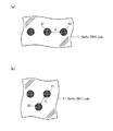
尚、本実施形態に係る光論理素子1(距離d=23.6nm)をHAADF-SREM(High-Angle Annular Dark-Field Scanning Transmission Electron Microscopy:高角度散乱暗視野走査透過電子顕微鏡法)により観察すると、例えば図5(a)に示すように、第1量子ドット層(下層)に含まれるInAs量子ドットの直上に、第2量子ドット層(上層)に含まれるInAs量子ドットが形成されていることがわかる。これは、中間層13(図1参照)の表面(上面)に、InAs量子ドット21に起因する歪みが生じるためである。
他方、比較例に係る光論理素子(距離d=34.4nm)をHAADF-SREMにより観察すると、例えば図5(b)に示すように、上層に形成されたInAs量子ドットは、下層に形成されたInAs量子ドットの影響をほとんど、又は全く受けないことがわかる。これは、中間層膜厚が比較的厚くなるため、下層に形成されたInAs量子ドットに起因する歪みが、中間層の表面に現れにくくなる又は現れないためである。
本実施形態に係る「InAs量子ドット21」及び「InAs量子ドット22」は、夫々、本発明に係る「第1量子ドット」及び「第2量子ドット」の一例である。
<変形例>
上述した実施形態では、InAs量子ドットが積層されている態様について説明したが、本発明は、例えば量子ドット層を1層のみ備える光論理素子にも適用可能である。この場合は、図6(a)及び(b)に示すように、GaAs基板11の上層に形成されたInAs量子ドット21及びInAs量子ドット22間の距離dを、上述した13nm~26nmの範囲内、望ましくは17nm~24nmの範囲内に設定すればよい。
上述した実施形態では、InAs量子ドットが積層されている態様について説明したが、本発明は、例えば量子ドット層を1層のみ備える光論理素子にも適用可能である。この場合は、図6(a)及び(b)に示すように、GaAs基板11の上層に形成されたInAs量子ドット21及びInAs量子ドット22間の距離dを、上述した13nm~26nmの範囲内、望ましくは17nm~24nmの範囲内に設定すればよい。
本発明は、上述した実施形態に限られるものではなく、請求の範囲及び明細書全体から読み取れる発明の要旨或いは思想に反しない範囲で適宜変更可能であり、そのような変更を伴う光論理素子もまた本発明の技術的範囲に含まれるものである。
1…光論理素子、11…GaAs基板、12…GaAsバッファ層、13…中間層、14…キャップ層、21、22…InAs量子ドット
Claims (3)
- 基板と、
前記基板上に配置され、近接場相互作用によりエネルギーを授受可能な第1量子ドット及び第2量子ドットと、
を備え、
前記第1量子ドット及び前記第2量子ドット間の距離が、13nm~26nmである
ことを特徴とする光論理素子。 - 前記第1量子ドット及び前記第2量子ドット間の距離が、17nm~24nmであることを特徴とする請求項1に記載の光論理素子。
- 前記第1量子ドット及び前記第2量子ドットは、前記第1量子ドットを構成する材料及び前記第2量子ドットを構成する材料とは異なる材料を含んでなる中間層を挟んで相対向するように、前記基板上に積層されていることを特徴とする請求項1に記載の光論理素子。
Priority Applications (1)
| Application Number | Priority Date | Filing Date | Title |
|---|---|---|---|
| PCT/JP2011/056596 WO2012127573A1 (ja) | 2011-03-18 | 2011-03-18 | 光論理素子 |
Applications Claiming Priority (1)
| Application Number | Priority Date | Filing Date | Title |
|---|---|---|---|
| PCT/JP2011/056596 WO2012127573A1 (ja) | 2011-03-18 | 2011-03-18 | 光論理素子 |
Publications (1)
| Publication Number | Publication Date |
|---|---|
| WO2012127573A1 true WO2012127573A1 (ja) | 2012-09-27 |
Family
ID=46878770
Family Applications (1)
| Application Number | Title | Priority Date | Filing Date |
|---|---|---|---|
| PCT/JP2011/056596 Ceased WO2012127573A1 (ja) | 2011-03-18 | 2011-03-18 | 光論理素子 |
Country Status (1)
| Country | Link |
|---|---|
| WO (1) | WO2012127573A1 (ja) |
Citations (1)
| Publication number | Priority date | Publication date | Assignee | Title |
|---|---|---|---|---|
| JPH07307454A (ja) * | 1993-09-16 | 1995-11-21 | Toshiba Corp | 量子効果装置、回転方式論理装置および半導体装置の製造方法 |
-
2011
- 2011-03-18 WO PCT/JP2011/056596 patent/WO2012127573A1/ja not_active Ceased
Patent Citations (1)
| Publication number | Priority date | Publication date | Assignee | Title |
|---|---|---|---|---|
| JPH07307454A (ja) * | 1993-09-16 | 1995-11-21 | Toshiba Corp | 量子効果装置、回転方式論理装置および半導体装置の製造方法 |
Non-Patent Citations (1)
| Title |
|---|
| KOICHI AKABANE ET AL.: "Tajusekiso InAs Ryoshi Dot ni Okeru Reiki Ido", DAI 57 KAI THE JAPAN SOCIETY OF APPLIED PHYSICS KANKEI RENGO KOENKAI, vol. 57, no. 3, 3 March 2010 (2010-03-03), pages 03-216 * |
Similar Documents
| Publication | Publication Date | Title |
|---|---|---|
| US9499400B2 (en) | Optical devices and methods of controlling propagation directions of light from the optical devices | |
| JP4871994B2 (ja) | 導波路に結合されるナノ粒子 | |
| Sanvitto et al. | Observation of ultrahigh quality factor in a semiconductor microcavity | |
| WO2007108218A1 (ja) | 2次元フォトニック結晶面発光レーザ | |
| US20180217331A1 (en) | A slow-light generating optical device and a method of producing slow light with low losses | |
| WO2013172161A1 (ja) | 光学素子及び光検出器 | |
| Huang et al. | Bright single photon emission from quantum dots embedded in a broadband planar optical antenna | |
| CN107329207B (zh) | 一种石墨烯-半导体双脊型混合表面等离子波导结构 | |
| CN106526725A (zh) | 一种基于半导体增益和石墨烯的spp装置 | |
| CN106165123A (zh) | 用于声子的电场控制元件 | |
| JP6901087B2 (ja) | 光デバイス及びその製造方法 | |
| Alfaraj et al. | Silicon‐Integrated Next‐Generation Plasmonic Devices for Energy‐Efficient Semiconductor Applications | |
| WO2012127573A1 (ja) | 光論理素子 | |
| JP5796074B2 (ja) | 近接場光デバイスの製造方法及び近接場光デバイス | |
| Bracher et al. | Optical study of lithographically defined, subwavelength plasmonic wires and their coupling to embedded quantum emitters | |
| CN107037535B (zh) | 一种金属-半导体双纳米线型混合表面等离子波导结构 | |
| Dufaux et al. | Surface plasmon coupling to nanoscale Schottky-type electrical detectors | |
| JP2009111167A (ja) | 面発光型半導体レーザ素子 | |
| Briscoe et al. | Surface-plasmon-polariton assisted modification of spontaneous emission of colloidal quantum dots in metal nanostructures | |
| Shneen et al. | Controllable surface Plasmon polariton propagation length using a suitable quantum dot material | |
| CN207992502U (zh) | 一种石墨烯-半导体双脊型混合表面等离子波导结构 | |
| CN107678080A (zh) | 一种可调谐的石墨烯纳米激光器 | |
| CN111175871B (zh) | 一种基于近对称保护型连续束缚态的亚波长光栅结构 | |
| Guo et al. | Numerical study of a high-resolution far-field scanning optical microscope via a surface plasmon-modulated light source | |
| EP4675495A1 (en) | Optical device |
Legal Events
| Date | Code | Title | Description |
|---|---|---|---|
| 121 | Ep: the epo has been informed by wipo that ep was designated in this application |
Ref document number: 11861484 Country of ref document: EP Kind code of ref document: A1 |
|
| NENP | Non-entry into the national phase |
Ref country code: DE |
|
| 122 | Ep: pct application non-entry in european phase |
Ref document number: 11861484 Country of ref document: EP Kind code of ref document: A1 |
|
| NENP | Non-entry into the national phase |
Ref country code: JP |