WO2012124606A1 - 非同期データ転送装置 - Google Patents
非同期データ転送装置 Download PDFInfo
- Publication number
- WO2012124606A1 WO2012124606A1 PCT/JP2012/055990 JP2012055990W WO2012124606A1 WO 2012124606 A1 WO2012124606 A1 WO 2012124606A1 JP 2012055990 W JP2012055990 W JP 2012055990W WO 2012124606 A1 WO2012124606 A1 WO 2012124606A1
- Authority
- WO
- WIPO (PCT)
- Prior art keywords
- wiring
- transmitter
- receiver
- mode
- failure
- Prior art date
- Legal status (The legal status is an assumption and is not a legal conclusion. Google has not performed a legal analysis and makes no representation as to the accuracy of the status listed.)
- Ceased
Links
Images






Classifications
-
- H—ELECTRICITY
- H04—ELECTRIC COMMUNICATION TECHNIQUE
- H04L—TRANSMISSION OF DIGITAL INFORMATION, e.g. TELEGRAPHIC COMMUNICATION
- H04L25/00—Baseband systems
- H04L25/02—Details ; arrangements for supplying electrical power along data transmission lines
- H04L25/0264—Arrangements for coupling to transmission lines
- H04L25/028—Arrangements specific to the transmitter end
- H04L25/0282—Provision for current-mode coupling
-
- H—ELECTRICITY
- H04—ELECTRIC COMMUNICATION TECHNIQUE
- H04L—TRANSMISSION OF DIGITAL INFORMATION, e.g. TELEGRAPHIC COMMUNICATION
- H04L25/00—Baseband systems
- H04L25/02—Details ; arrangements for supplying electrical power along data transmission lines
- H04L25/0264—Arrangements for coupling to transmission lines
- H04L25/0292—Arrangements specific to the receiver end
- H04L25/0294—Provision for current-mode coupling
Definitions
- the present invention relates to an asynchronous data transfer apparatus. More particularly, the present invention relates to an asynchronous data transfer device having delay time and wiring fault tolerance.
- SoC system-on-chip
- a system LSI is generally composed of an IP core (Intellectual Property Core), which is a plurality of processing function units.
- IP cores such as arithmetic, digital signal arithmetic (DSP), and memory can be integrated in one chip of a system LSI.
- DSP digital signal arithmetic
- a method of communicating between these IP cores via a router arranged adjacent to the IP core based on packet information is called a network-on-chip (NoC) (Non-Patent Document 1). reference).
- Each IP core arranged in one chip in the network on chip operates at the clock frequency of each IP core. That is, each IP core normally operates at a different clock frequency.
- As a communication method between IP cores there are a synchronous method using a clock used in bus communication and an asynchronous communication method using no clock. The synchronous method has no design freedom and consumes a lot of power.
- This asynchronous communication method includes a four-phase method and a two-phase method (see Non-Patent Documents 2 and 3).
- a four-phase protocol is used, and a router and a communication link are designed using a pseudo-delay-insensitive logic method (hereinafter also referred to as QDI logic type) (non-delayed).
- QDI logic type pseudo-delay-insensitive logic method
- the total wiring length in one chip of the system LSI is 1 km (see Non-Patent Document 5). Not only does the number of wires increase further, but open failures due to electromigration of wires are becoming a serious problem, and it is necessary to examine the reliability of the wires (see Non-Patent Documents 5 to 8). ).
- FIG. 17 is a block diagram showing a configuration of a conventional asynchronous data transfer apparatus 100.
- FIG. 17A shows a case where the wiring is normal
- FIG. 17B shows a case where the wiring has an open failure.
- an internal wiring 103 is formed between a plurality of adjacent modules 101 and 102 in the LSI.
- Modules 101 and 102 are, for example, IP cores.
- the internal wiring 103 is formed of a wiring layer using copper (Cu) in the current technology.
- Cu copper
- FIG. 18 is a diagram showing a communication link in an asynchronous data transfer device of QDI logic type. As shown in this figure, communication is performed between the modules 101 and 102 by handshaking based on a request (request) -acknowledgment (reception confirmation). First, the left module 101 transmits data having request information from the input port, that is, (DATA + REQ). Second, the right module 102 receives the transmitted data at the output port, and then transmits an acknowledgment signal (hereinafter referred to as an ACK signal) serving as reception confirmation information to the left module.
- an acknowledgment signal hereinafter referred to as an ACK signal
- FIG. 19 is a diagram showing a problem of a conventional method for detecting a wiring fault in an output port.
- data is received when all input data is detected at the output port of the module. Even if only one bit of data is not received, no data is received. This loss of 1 bit is caused by a wiring failure or a delay failure. However, these two failures cannot be distinguished at the output port of the module. Since no data is received when a wiring failure occurs, communication becomes fatal. In order to prevent a fatal state, a temporal assumption for detecting a wiring failure is effective.
- the asynchronous data transfer apparatus is not of the QDI logic type as shown in the output port of Table 1. Therefore, it is impossible for the QDI logic type asynchronous data transfer device to detect only a wiring failure at the output port.
- Non-Patent Document 9 proposes a method of replacing a failed wiring with a normal wiring at the time of a wiring failure, but does not specify the failure detection method.
- Non-Patent Document 10 permanent failure detection is performed by duplicating data transfer and comparing the two data, but the data transfer function cannot be recovered.
- Non-Patent Document 11 the data transfer is triplicated and the majority of the data is taken to detect the wiring fault and maintain (recover) the data transfer function.
- the detection method is within a certain time range, that is, a delay. Since it is based on assumptions, coexistence of delay fault tolerance and wiring fault tolerance has not been realized.
- Non-Patent Documents 12 and 13 propose to deal with wiring failures at an algorithm level instead of a circuit level as in Non-Patent Documents 9 to 11.
- Non-Patent Document 9 proposes a method of replacing a failed wiring with a normal wiring at the time of a wiring failure as described above.
- the failure detection method is not specified.
- Non-Patent Document 10 permanent failure detection is performed, but the data transfer function cannot be recovered.
- Non-Patent Document 11 since the detection method is based on a delay assumption within a certain time range, that is, not the QDI logic type, coexistence of delay fault tolerance and wiring fault tolerance is not realized.
- the reliability of the circuit during operation may be reduced due to variations in semiconductor process, power supply voltage, and temperature.
- wiring faults cannot be detected. Even if a wiring failure can be detected, it takes a long time to detect the wiring failure, so the influence on the operation of the entire network-on-chip system becomes very large. For this reason, it is difficult to realize a network-on-chip having high reliability.
- an object of the present invention is to provide an asynchronous data transfer apparatus that can detect a wiring fault without delay assumption by monitoring the amount of current and has both a delay fault tolerance and a wiring fault tolerance.
- an asynchronous protocol conversion device includes an LSI asynchronous data transfer device disposed between IP cores, a first wiring connected to the first IP core, and a second wiring A second wiring connected to the IP core, a transmitter connected to the first wiring, a receiver connected to the second wiring, and a third wiring connecting the transmitter and the receiver;
- the transmitter includes an input unit having an encoder and an input control unit, and an output unit, and the encoder of the transmitter is a current driver that detects an open fault in the third wiring.
- a circuit is provided.
- the receiver preferably includes an input unit and an output unit including a decoder and an output control unit.
- the transmitter and receiver preferably operate in a pseudo delay insensitive logic manner.
- the encoder preferably includes a current source, an inverter connected to the current source, a current mirror circuit connected to the inverter, and an inverter connected to the current mirror circuit.
- the decoder preferably includes a current mirror circuit and an inverter connected to the current mirror circuit.
- an IN signal is input to the input unit of the transmitter
- a DATA signal and an ERR_DATA signal are output from the input unit to the receiver
- an OUT signal is output from the output unit of the receiver.
- a DATA BLOCK is composed of an IN signal, a DATA signal, an ERR_DATA signal, and an OUT signal, and the DATA BLOCK performs operations in a normal mode, a failure mode, a configuration mode, and a recovery mode.
- a wiring failure is detected by the encoder, the transmitter transitions to the failure mode, and in the failure mode, the transmitter sends the failure information to the receiver.
- the receiver transitions to failure mode
- the transmitter transitions to configuration mode based on the recovery code
- the transmitter transmits the recovery code to the receiver
- the receiver transitions to the configuration mode
- the transmitter is reconfigured to eliminate the wiring having a wiring fault based on the recovery code in the configuration mode
- the transmitter transitions to the recovery mode.
- the receiver transitions to the recovery mode by the signal from the transmitter, and in the recovery mode, the signal from the transmitter to the receiver replaces the wiring having a wiring fault with a normal wiring. Sending It is.
- asynchronous data transfer can be performed without delay assumption, that is, without delay assumption by monitoring the current amount as described above, and the delay fault tolerance and monitoring of the current amount on the input side can be detected.
- the detection can be performed at high speed. Therefore, the influence on the operation of the entire network-on-chip system at the time of the wiring fault can be minimized.
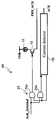
- FIG. 2 is a diagram illustrating an architecture of a communication link of the present invention. It is a circuit diagram of the input control part of a transmitter.
- FIG. 4 is a block diagram of a decoder in the receiver. It is a figure explaining operation
- Asynchronous data transfer device 2 Transmitter 3: Wiring 3a: First wiring 3b: Second wiring 3c: Second wiring 4: Receiver 5: Encoder 5a, 5b: AND circuit 5c: OR circuit 5d : First multiplexer 5e: second multiplexer 6: input control units 6a, 6b: OR circuits 6c, 6d, 6e: AND circuits 6f, 6g: asynchronous RS latches 6h, 6i, 6j, 6k, 6l, 6m: Asynchronous G latch 6n: multiplexer 7: decoder 7a: AND circuit 7b: multiplexer 7c: C element 8: output control unit 8a: pass transistors 8b, 8c: asynchronous RS latches 8d, 8e, 8f: AND circuits 8g, 8h, 8i, 8j, 8k: OR circuit 11: Driver circuits 11a, 11b, 11c, 11d: Current driver circuit 12: Current source 13, 15: Inverter 14: Karen Mirror circuit 16, 17: current receiving circuit 18: OR circuit 11
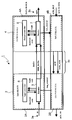
- FIG. 1 is a block diagram showing a configuration of an asynchronous data transfer apparatus 1 according to the present invention.
- an asynchronous data transfer apparatus 1 according to the present invention includes a first wiring 3a connected to a first IP core described later and a second wiring described later in an LSI disposed between IP cores.
- a second wiring 3b connected to the IP core, a transmitter 2 connected to the first wiring 3a, a receiver 4 connected to the second wiring 3b, a transmitter 2 and a receiver 4,
- a third wiring 3c for connecting the two.
- the transmitter 2 includes an input unit (INPUT BLOCK) 2A to which an IN signal is input and an output unit (OUTPUT BLOCK) 2B.
- the input unit 2A includes an encoder 5 to which an IN signal is input, and an input control unit 6 connected to the encoder 5.
- the receiver 4 includes an output unit (OUTPUT BLOCK) 4A to which a DATA signal and an ERR_DATA signal are input from the transmitter 2, and an input unit (INPUT BLOCK) 4B.
- the output unit 4 ⁇ / b> A includes a decoder 7 to which the DATA signal and the ERR_DATA signal are input from the transmitter 2, and an output control unit 8 connected to the decoder 7.
- the IN signal input to the input unit 2A of the transmitter 2, the DATA signal and the ERR_DATA signal output from the input unit 2A of the transmitter 2 and received by the output unit 4A of the receiver 4, and the output unit 4A of the receiver 4 are collectively referred to as DATA BLOCK (data block).
- ACK_IN signal output from the output unit 2B of the transmitter 2 the ACK signal and the ERR_ACK signal transmitted from the input unit 4B of the receiver 4 to the output unit 2B of the transmitter 2, and the input to the input unit 4B of the receiver 4 ACK_OUT signals to be transmitted are collectively called ACK BLOCK (acknowledge block).
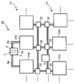
- FIG. 2 is a block diagram showing a configuration of the LSI 20 in which the asynchronous data transfer apparatus 1 of the present invention is arranged.
- the LSI 20 disposed as shown in the figure includes a plurality of IP cores 21 and the asynchronous data transfer apparatus 1 of the present invention disposed adjacent to the plurality of IP cores 21.
- the transmitter 2 of the asynchronous data transfer apparatus 1 is connected to the first IP core 21a via the first wiring 3a.
- the receiver 4 of the asynchronous data transfer apparatus 1 is connected to the second IP core 21b via the second wiring 3b.
- the asynchronous data transfer apparatus 1 is a communication link between the IP core 21a and the IP core 21b.
- the asynchronous data transfer device 1 may be inserted between the IP cores 21, for example, between the wirings connected between the IP core 21 c and the IP core 21 d and connected between the router 22 that transmits and receives asynchronous data.
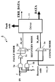
- FIG. 3 is a block diagram of the encoder 5 in the transmitter 2 shown in FIG.
- the encoder 5 includes a first AND circuit 5a and a second AND circuit 5b to which an IN signal is connected, an OR circuit 5c to which an output of the first AND circuit 5a is input, an output of the OR circuit 5c, and the like. Is input to the first multiplexer 5d, the second multiplexer 5e to which the output of the second AND circuit 5b and the like are input, and the driver circuit 11 to which the outputs of the first and second multiplexers 5d and 5e are input. And is composed of.
- the IN signal is 1-of-4 encoded (see Non-Patent Document 12).
- the signs of the IN signal and the DATA signal are the same.
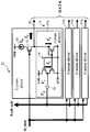
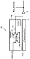
- FIG. 4 is a circuit diagram of the driver 11 in the encoder 5.
- the driver circuit 11 includes four current driver circuits 11a, 11b, 11c, and 11d.
- the current driver circuit 11a includes a current source 12 connected to the power supply Vdd, an inverter 13 connected to the current source 12, a current mirror circuit 14 connected to the source of the inverter 13, and an output of the current mirror circuit 14. And an inverter 15 connected to the.
- I in is separated into I w and I d when there is no wiring failure.
- the voltage level Vd is low.
- the wiring 3c flowing I w is I d increases since open. Since I d is copied to I c using the current mirror circuit 14, V c drops with a large I d .
- V d becomes high by the inverter 15, and the high signal V d generates a fault code.
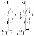
- FIG. 5 is a circuit diagram for explaining that a wiring fault insensitive to the delay time can be detected based on the current monitoring of the present invention.
- FIG. 5A shows a case where there is no fault in the wiring 3c
- FIG. 5B shows a wiring 3c. Shows a case where an open failure occurs.
- FIG. 5 (a) when there is no fault in the wiring 3c at the input ports, current I in is separated into transmission current I w and the detected current I d.
- the I out transmission current I w flows through the wiring 3c.
- the resistance of the wiring 3c increases with time due to electromigration, the transmission current Iw decreases and the detection current Id increases.
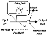
- FIG. 6 is a diagram showing the link architecture of the present invention.
- the information on the wiring failure is obtained by feedback on the input side of the transmitter 2. Since there is no need to distinguish between wiring faults and delay faults, wiring faults can be detected without making temporal assumptions. Thereby, as shown in Table 8 to be described later, it is insensitive to the delay time, that is, it is possible to detect a wiring failure with the QDI logic type.
- FIG. 7 is a circuit diagram of the input control unit 6 of the transmitter 2.
- the input controller 6 includes two OR circuits 6a and 6b, three AND circuits 6c, 6d and 6e, two asynchronous RS latches 6f and 6g, and six asynchronous G latches 6h and 6i. , 6j, 6k, 6l, 6m and a multiplexer 6n.
- Table 2 shows the 1-of-4 code for DATA BLOCK during the normal mode.
- the data is represented by a 4-bit code word (code word).
- FIG. 8 is a circuit diagram of the output unit 2B of the transmitter 2.
- the output unit 2B includes a current receiving circuit 16 to which an ERR_ACK signal is input, a current receiving circuit 17 to which an ACK signal is input, and an OR circuit 18 to which outputs of the current receiving circuits 16 and 17 are input.
- the current receiving circuit 16 includes a current mirror circuit 14 and an inverter 15 connected to the current mirror circuit 14.
- the current receiving circuit 17 is configured similarly to the current receiving circuit 16.
- FIG. 9 is a circuit diagram of the decoder 7 in the receiver 4.
- the decoder 7 includes a detector 19 to which a DATA signal and an ERR_DATA signal are input, an AND circuit 7a to which an Out # data signal and a failure mode signal which are outputs of the detector 19 are input, and an output of the AND circuit 7a.
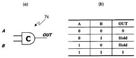
- FIG. 10A and 10B are diagrams for explaining the operation of the C element 7c.
- FIG. 10A is a circuit diagram showing the configuration of the C element 7c
- FIG. 10B shows a truth table of the operation of the C element 7c.
- the C element 7c is a bistable storage element used in an asynchronous circuit, and is also called a waiting circuit or a junction circuit.
- FIG. 10B when all inputs become logic “1”, the output becomes logic “1”, and when all inputs become logic “0”, the output becomes logic “0”. In the state where logic “1” and “0” are mixed in the input, the previous output is maintained.
- FIG. 11 is a circuit diagram of the detector 19 in the decoder 7.
- the detector 19 includes four current detectors 19a, 19b, 19c, and 19d.
- Each of the current detectors 19a to 19d includes a current mirror circuit 14 to which a DATA signal is input and an inverter 15 connected to the output of the current mirror circuit 14.
- the current detector 19e to which the ERR_DATA signal is input also has the same configuration as the current detector 19a.
- the current detector 19a converts the current Iout into a voltage Vout .
- the sign of the DATA signal and the OUT signal is the same.
- the ERR_DATA signal becomes “1”. “1” means “failure”.
- the mode transitions to the failure mode.
- the recovery code is stored in the receiver 4 when the recovery code is transmitted from the transmitter 2. This stored data changes the mode to the configuration mode.
- the output selector composed of the multiplexer 7b in FIG. 9 the connection between (DATA, ERR_DATA) and OUT is reestablished so as to exclude the wiring 3c having an open fault from the wiring 3c based on the recovery code. Composed.
- the data is then transmitted by a 1-of-5 code that passes through DATA, ERR_DATA. Then, the mode transitions to the recovery mode.
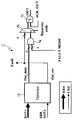
- FIG. 12 is a circuit diagram of the output control unit 8 of the receiver 4.
- the output control unit 8 includes a first asynchronous RS latch 8b, a second asynchronous RS latch 8c, and three AND circuits 8d, 8e, and 8f, to which a signal from the decoder 7 is input via the pass transistor 8a. And 5 OR circuits and 8g, 8h, 8i, 8j, and 8k.
- FIG. 13 is a circuit diagram of the input unit 4B of the receiver 4.
- the input unit 4B includes two AND circuits 25 connected to Ack # internal, an inverter 13 connected to the output of the first AND circuit 25a, a current source 12 connected to the inverter 13, and a second AND circuit.
- the current detector 19f is connected to the output of the circuit 25b.
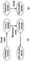
- FIG. 14 is a diagram illustrating the modes of DATA BLOCK and ACK BLOCK, where (a) shows four modes of DATA BLOCK and (b) shows two modes of the ACK BLOCK block.
- the normal mode NVMAL
- the failure mode FAULT
- the configuration mode CONFIG
- CONFIG configuration mode
- CONFIG configuration mode
- CONFIG configuration mode
- RECOVERY recovery mode
- FIG. 14B in the ACK BLOCK, the normal mode (NORMAL) and the recovery mode (RECOVERY) are performed depending on the state of the wiring 3c used for transmission and reception of the ACK BLOCK signal.
- the communication link uses a 4-phase code. Data transmission between the transmitter 2 and the receiver 4 is performed by a current mode signal, and other circuits use a voltage mode signal.
- FIG. 15 is a timing chart of a system that recovers from a failure.
- one wiring 3c related to the data “3” among the wirings 3c is open.
- DATA BLOCK and ACK BLOCK are operating in normal mode.
- the DATA BLOCK mode will be described.
- the operation is based on the 1-of-4 code.
- Table 3 shows a two-line code for ACK BLOCK.
- the transmitter 2 detects the ACK signal and transmits (0, 0, 0, 0) as a spacer to the receiver 4.
- the receiver 4 detects the spacer and transmits (0, 0) as a spacer to the transmitter 2.
- the 4-phase protocol requires 4 steps per communication.
- DATA BLOCK uses a four-phase protocol.
- Table 4 shows the 1-line code for DATA BLOCK during failure mode.
- the ERR_DATA signal is represented by a 1-bit code word.
- the transmitter 2 transmits failure information (Fault) to the receiver 4 as failure information.
- failure code failure code
- the transmitter 2 changes to the failure mode.
- the DATA signal does not change from (0, 0, 0, 0).
- the recovery code is generated based on the fault code.
- the receiver 4 detects the fault information (Fault)
- the mode of the receiver 4 transitions to the fault mode, and the preparation for receiving the recovery code is completed in the configuration mode which is the next mode. Then, the mode of the transmitter 2 transitions to the recovery mode.
- Table 5 shows the 1-of-4 code for DATA BLOCK during the configuration mode.
- the recovery code is generated in order to eliminate the wiring 3c having an open failure.
- the receiver 4 When the receiver 4 changes to the configuration mode, the open wiring 3c related to the data “3” is replaced by the wiring 3c of the ERR_DATA signal. In the configuration mode, the receiver 4 replaces a wiring having a wiring failure with a normal wiring based on the recovery code. Finally, the mode of the transmitter 2 transitions to the recovery mode.
- Table 6 shows the 1-of-5 code for DATA BLOCK during the recovery mode.
- the transmitter 2 transmits (0, 0, 0, 0, 1) to the receiver 4 as data “3”.
- the receiver 4 recognizes (0, 0, 0, 0, 1) as data “3”, and as a result, operates in the recovery mode.
- the operation is performed in the recovery mode in which data transfer is performed under a wiring failure related to the data “3”.
- the output of the encoder 5 becomes a recovery code. Since the recovery code is generated using the wiring 3c having no failure, the failure code returns to (0, 0, 0, 0).
- the connection between (DATA, ERR_DATA) and IN has an open failure in the wiring 3c based on the recovery code. Reconfigured to eliminate one wiring that has.
- the data of the DATA signal and the ERR_DATA signal is transmitted by a 1-of-5 code.
- a signal from the transmitter 2 to the receiver 4, for example, an ERR_DATA signal is transmitted by replacing a wiring having a wiring failure with a normal wiring.
- the ACK BLOCK mode With respect to the ACK signal, the failure-recovery mode transitions as shown in FIG. First, the ACK signal is operating in normal mode.
- the two-line code of ACK BLOCK changes from (1, 0) to (0, 1) as shown in Table 3.
- the output unit 2B of the transmitter 2 detects the Acknowledgment information by the logical sum of the two-line codes in any mode, so that the Acknowledgment information is received under a wiring failure of the ACK BLOCK. Acknowledgment information is also called confirmation information.
- the asynchronous data transfer apparatus 1 of the present invention it is possible to realize detection of an open (permanent) failure of the wiring based on the monitoring of the current amount. That is, during data transfer, the input current is divided into a “data transfer current” I w to the receiving side and a “feedback current” I d for monitoring. Since the total value of the two current amounts is constant, the “data transfer current” I w is cut off at the time of a wiring failure, while the “feedback current” I d increases monotonously. By detecting an increase in “feedback current” I d on the transmission side, it becomes possible to detect a wiring failure without assuming a delay.
- the function as the asynchronous data transfer apparatus 1 is restored by replacing the detected faulty wiring with the spare normal wiring 3c.
- the asynchronous data transfer apparatus 1 of the present invention can realize wiring fault tolerance while having the delay fault tolerance of QDI logic type asynchronous data transfer.
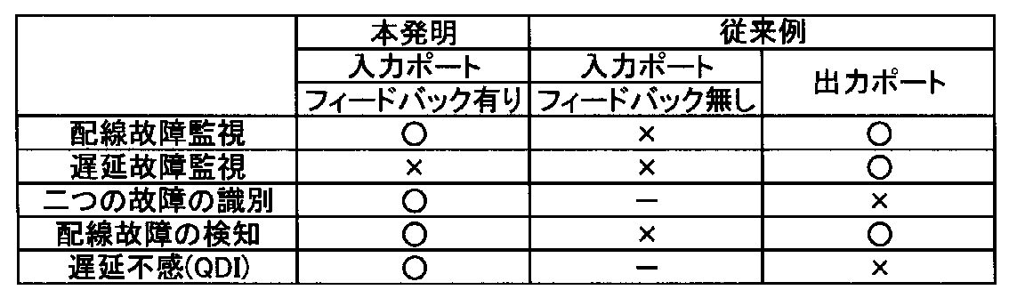
- Table 7 shows the functions of the asynchronous data transfer apparatus 1 of the present invention. Table 7 also shows the functions of the conventional asynchronous data transfer apparatus shown in Table 1. As shown in Table 7, in the asynchronous data transfer apparatus 1 of the present invention, it is possible to perform wiring failure monitoring and detection at an input port, which has not been possible in the past, in the QDI logic type.
- a circuit of the asynchronous data transfer apparatus 1 of the present invention was created by a 0.13 ⁇ m CMOS technology of Silterra and evaluated by HSPICE.
- the length of the wiring 3c between the transmitter 2 and the receiver 4 is 1 mm.
- the wiring 3c was simulated with a pie model. As parameters of the pie model, the resistance was 91 ⁇ / mm and the capacitance was 84 fF / mm.
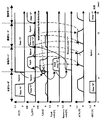
- FIG. 16 is a timing chart of the simulation.
- FIG. 16 shows a case where the wiring 3c has a failure of Data “3”.
- I in was 165 ⁇ A.
- I d increases. Transition to the failure mode so that this I d restores the communication link.
- Table 8 is a table comparing the present invention with comparative examples. As shown in Table 8, in the case of the present invention, wiring failure detection and operation correction under a wiring failure, that is, recovery is possible. It also supports the QDI logic type that is insensitive to delay time. The number of wirings was 2n + 3 for n bits, and the number of transistors used was 1280. The throughput was 837 Mbps, the power consumption was 584 ⁇ W, and the energy was 698 fJ / bit.
- the conventional example using the 1-of-4 code supports the QDI logic type, but cannot detect a wiring failure and correct the operation under a wiring failure.
- the number of wirings was 2n + 1 for n bits, and the number of transistors used was 545.
- the throughput was 840 Mbps, the power consumption was 328 ⁇ W, and the energy was 388 fJ / bit.
- the conventional example using the duplicated 1-of-4 code does not support the QDI logic type, but can detect a wiring fault but cannot correct the operation under a wiring fault. It is.
- the number of wirings was 2 ⁇ (2n + 1) for n bits, and the number of transistors used was 1049.
- the throughput was 741 Mbps, the power consumption was 616 ⁇ W, and the energy was 831 fJ / bit.
- the conventional example using the tripled 1-of-4 code does not correspond to the QDI logic type, but detects a wiring fault and corrects the operation under a wiring fault as in the present invention. In other words, recovery is possible.
- the number of wires was 3 ⁇ (2n + 1) for n bits, and the number of transistors used was 1223.
- the throughput was 622 Mbps, the power consumption was 761 ⁇ W, and the energy was 1223 fJ / bit.
- the asynchronous data transfer apparatus 1 having delay and wiring fault tolerance according to the present invention is compatible with the QDI logic type that is insensitive to the delay time, and can detect the wiring fault and recover the faulty wiring.
- the number of transistors used in the asynchronous data transfer device 1 of the present invention is the number between the comparative example 2 and the comparative example 3, but the throughput is as high as the comparative example 1.
- the power consumption was lower than Comparative Examples 2 and 3. Further, even when the number of transistors is expanded to n bits, the input control unit 6 and the output control unit 8 do not depend on the bit width, so that the number of transistors is smaller than those in the second and third comparative examples.
- the network-on-chip using the asynchronous data transfer device 1 of the present invention not only has resistance to delay fluctuations due to process, power supply voltage, and temperature fluctuations, but also has wiring fault tolerance due to aging degradation of the LSI 20.
- a highly reliable system can be realized. Therefore, it can be used for in-vehicle and space system-on-chip (SoC) which is expected to be used in harsh environments. It can also be applied to 4th generation mobile phones.
- SoC space system-on-chip
- the asynchronous data transfer apparatus 1 is an asynchronous type that does not use a clock signal, it is possible to reduce the power accompanying the deletion of the circuit that generates the clock signal, so that the power of the system can be reduced. .
Landscapes
- Engineering & Computer Science (AREA)
- Power Engineering (AREA)
- Computer Networks & Wireless Communication (AREA)
- Signal Processing (AREA)
- Dc Digital Transmission (AREA)
- Manipulation Of Pulses (AREA)
Abstract
電流量の監視による遅延仮定なしで配線故障の検出ができ、遅延故障耐性と配線故障耐性を同時に有する非同期データ転送装置を提供する。IPコア間に配設するLSIの非同期データ転送装置1において、第1のIPコアに接続する第1の配線3aと、第2のIPコアに接続する第2の配線3bと、第1の配線3aに接続する送信器2と、第2の配線3bに接続する受信器4と、送信器2と受信器4とを接続する第3の配線3cと、を含み、送信器2は、符号器5と入力制御部6とを有する入力部2Aと、出力部2Bと、を含み、送信器2の符号器5は、第3の配線3cのオープン故障を検出する電流ドライバ回路11a,11b,11c,11dを備える。
Description
本発明は、非同期データ転送装置に関する。さらに、詳しくは、本発明は、遅延時間及び配線故障耐性を有する、非同期データ転送装置に関する。
半導体集積回路は、最小加工寸法の微細化が進み、量産レベルの最小加工寸法は32nmに達しており、集積されるトランジスタ数の規模が大きくなっている。このような大規模集積回路は、システムLSIとも呼ばれている。システムLSIは、システムオンチップ(System-on-Chips:SoC)とも呼ばれている。
システムLSIは、一般に複数の処理機能単位であるIPコア(Intellectual Property Core)で構成されている。近年の最小加工寸法の微細化によって、システムLSIの1チップ中には演算、デジタル信号演算(DSP)、メモリ等のIPコアが集積できるようになっている。これらIPコア間をパケット情報に基づき、IPコアに隣接して配設されるルーターを介して通信する方式がネットワークオンチップ(Network-on-Chip:NoC)と呼ばれている(非特許文献1参照)。
ネットワークオンチップ内の1チップ中に配置される各IPコアは、各IPコアのクロック周波数で動作している。つまり、各IPコアは、通常異なるクロック周波数で動作している。各IPコア間の通信方式としては、バス通信等で用いられるクロックによる同期方式とクロックを用いない非同期通信方式がある。同期方式では、設計自由度がなく消費電力が多い。
近年、各IPコア間の通信方式としては、上記した従来の同期方式の欠点を改善するため、非同期通信方式が採用されることが多くなってきている。この非同期通信方式にも4相方式と2相方式がある(非特許文献2,3参照)。
4相の非同期通信方式では、4相方式のプロトコルを用い、擬似遅延不感の論理方式(quasi-delay-insensitive、以下、QDI論理型とも呼ぶ。)によるルーターや通信リンクが設計されている(非特許文献4参照)。
さらに、システムLSIの1チップ中の総配線長は、1kmにもなってきている(非特許文献5参照)。配線数はさらに増加するだけでなく、配線のエレクトロマイグレーションによるオープン(断線)の故障が深刻な問題になりつつあり、配線の信頼性に対する検討が必要になっている(非特許文献5~8参照)。
図17は、従来の非同期データ転送装置100の構成を示すブロック図であり、(a)は配線が正常な場合、(b)は配線がオープン故障の場合を示している。
図17(a)に示すように、非同期データ転送装置100は、LSI中の隣接する複数のモジュール101、102との間に内部配線103が形成されている。モジュール101、102は、例えばIPコアである。故障が無い場合には、モジュール101とモジュール102との間で非同期通信が行われている。内部配線103は、現状の技術では、銅(Cu)を用いた配線層で形成されている。
しかしながら、図17(b)に示すように、トランジスタの動作中に、エレクトマイグレーションによってCu配線に空孔(ボイドとも呼ぶ。)が生じた場合には、配線103にオープンの故障が生じる(非特許文献6参照)。さらに、加工寸法の微細化によって電流密度が増加するので、オープンによる故障の問題は、将来の技術ではよりクリチカルになる(非特許文献7参照)。
図18は、QDI論理型の非同期データ転送装置における通信リンクを示す図である。この図に示すように、通信はモジュール101と102との間で、リクエスト(要求)-アクノレッジ(受信確認)に基づくハンドシェイキングによって行われている。
最初に、左のモジュール101は、入力ポートからリクエスト情報を有しているデータ、つまり、(DATA+REQ)を送信する。
第2に、右のモジュール102は、送信されたデータを出力ポートで受信し、それから、受信確認情報となるアクノレッジ信号(以下、ACK信号と呼ぶ。)を左側のモジュールに送信する。
最初に、左のモジュール101は、入力ポートからリクエスト情報を有しているデータ、つまり、(DATA+REQ)を送信する。
第2に、右のモジュール102は、送信されたデータを出力ポートで受信し、それから、受信確認情報となるアクノレッジ信号(以下、ACK信号と呼ぶ。)を左側のモジュールに送信する。
ファンアウトの点における配線は大凡等しい遅延時間でなければならないという仮定の上記QDI型論理では、時間的な制約がないので、非同期回路はプロセスばらつき及び電圧と温度との変動によって生じる遅延故障に対して影響を受けないという利点がある(非特許文献4)。
しかしながら、配線故障のような永久故障は、QDI論理型の非同期データ転送装置にとって致命的な状態となる。それぞれの通信リンクにおいて、その出力が変わる前には(DATA+REQ)信号又は(ACK)信号に対して待機しているので、配線故障によって(DATA+REQ)信号又は(ACK)信号が変化しないときは、出力は決して変わらない。
しかしながら、配線故障のような永久故障は、QDI論理型の非同期データ転送装置にとって致命的な状態となる。それぞれの通信リンクにおいて、その出力が変わる前には(DATA+REQ)信号又は(ACK)信号に対して待機しているので、配線故障によって(DATA+REQ)信号又は(ACK)信号が変化しないときは、出力は決して変わらない。
図19は、出力ポートにおける従来の配線故障を検出する方法の問題点を示す図である。QDI論理型の論理では、入力される全てのデータがモジュールの出力ポートで検出されたときに、データが受信される。もしも、ただの1ビットのデータが受信されない場合でも、データが受信されない。この1ビットの喪失は、配線故障又は遅延故障によって発生する。しかしながら、これらの二つの故障は、モジュールの出力ポートで見分けることができない。配線故障が発生した場合にはデータが受信されないので、通信は致命的な状態となる。致命的な状態を防止するためには、配線故障を検出する時間的な仮定が有効となる。
しかしながら、時間的な仮定をした場合には、表1の出力ポートに示すように、非同期データ転送装置がQDI論理型ではなくなる。従って、出力ポートにおいてQDI論理型の非同期データ転送装置が配線故障だけを検出することは、不可能である。

配線故障だけを検出するためは、配線故障と遅延故障とを区別する必要がある。遅延故障は、送信された信号だけに影響するので、遅延故障は入力ポートでは無視できる。QDI論理型の非同期データ転送装置が配線故障だけを検出するためには、入力ポートにおいて配線故障を検出する必要がある。しかしながら、表1の入力ポートに示すように、従来のアーキテクチャーでは、入力ポートにおいて配線故障と遅延故障の両方とも検出できなかった。
非特許文献9には、配線故障時に、故障の配線を正常の配線と入れ替える方法が提案されているが、その故障検出方法については明記されていない。
非特許文献10には、データ転送を二重化しその二つのデータを比較することで永久故障検出を行っているが、データ転送機能の回復を行うことができない。
非特許文献11では、データ転送を三重化し、そのデータの多数決を取ることで、配線故障検出およびデータ転送機能の維持(回復)を行っているが、その検出方法はある時間範囲内、つまり遅延仮定に基づいているため、遅延故障耐性と配線故障耐性の両立は実現されていない。
非特許文献12及び13には、非特許文献9~11のように回路的なレベルではなく、アルゴリズムレベルで配線故障に対応することが提案されている。
L. Benini and G. De Micheli, "Networks on chips: A new SoC paradigm," IEEE Trans. Comput., vol. 35, no.1, pp.70-78, Jan. 2002
M. Krstic, et al., "Globally asynchronous locally synchronous circuits: Overview and outlook," IEEE Des. Test Comput., vol. 24, no.5, pp.430-441, Sep./Oct. 2007
D. Lattard, E. Beigne, R. Clemidy, Y. Durand, R. Lemaire, P. Vivet, and F. Berens, "A Reconfigurable Baseband Platform Based on an Asynchronous Network-on-Chip," IEEE J. Solid-State Circuits (JSSC), vol.43, no.1, Jan. 2008
J. Sparso, and S. Furber, "Principles of Asynchronous Circuit Design," Kluwer Academic Publisher, pp.9-28, 2001
International Technology Roadmap for Semiconductors, 2007 edition, Interconnect Chapter; http://www.itrs.net/Links/2QQ1ITRS/2007#Chapters/2007#Interconnect.pdf
J. Gill, T. Sullivan, S. Yankee, H. Barth and A. von Glasow, "Investigation of via-dominated multi-modal electromigration failure distributions in dual damascene Cu interconnects with a discussion of the statistical implications," Proc. Int. Ref. Phys. Symp., pp.298-304, 2002
Z. Choi, M. Tsukasa, J. M. Lee, G. -H. Choi, S. Choi and J. -T. Moon, "Effect of pre-existing void in sub-30nm Cu Interconnect Reliability," Proc. IEEE Int. Reliability Physics Symposium (IRPS), pp.903-905, 2010
Y. Ohtake, N. Onizawa, and T. Hanyu, "High-Performance Asynchronous Intra-Chip Communication Link Based on a Multiple-Valued- Current-Mode Single-Track Scheme," Proc. IEEE Int. Symp., Circuits and Systems, pp.1000-1003, Taipei, Taiwan, May 2009
T Lehtonen, P. Liljeberg and J. Plosila, "Online Reconfigurable Self-Timed Links for Fault Tolerant NoC," VLSI Design, vol. 2007, Article ID 94676, 2007
T. Verdel and Y. Makris, "Duplication-Based Concurrent Error Detection in Asynchronous Circuits: Shortcomings and Remedies," Proc. IEEE Int. Symp. Defect and Fault Tolerance in VLSI Systems 2002, pp.345-353, 2002
S. Almukharizim and O. Sinanoglu, "A Hazard-Free Majority Voter for TMR-Based Fault Tolerance in Asynchronous Circuits," Proc. Design and Test Workshop 2007, pp.93-98, 2007
V. Puente, J. A. Gregorio, F. Vallejo and R. Beivide, "Immunet: A cheap and robust fault-tolerant packet routing mechanism," ACMSIGARCH Computer Architecture News, 32(2):198, 2004
D. Fick, A. DeOrio, G. Chen, V. Bertacco, D. Sylvester and D. Blaauw, "A Highly Resilient Routing Algorithm for Fault-Tolerant NoCs," Proc Design, Automation and Test in Europe, 2009, pp.21-26, 2009
W. J. Bainbridge, and S. B. Furber, "Delay Insensitive System-on-Chip Interconnect using l-of-4 Data Encoding," Proc. 7th IEEE Int. Symp. Asynchronous Circuits Syst., pp.74-82, Mar. 2001
従来の回路レベルでの配線故障の対応方法(非特許文献9~11)において、非特許文献9では、前述の通り、配線故障時に、故障の配線を正常の配線と入れ替える方法が提案されているが、故障検出方法については明記されていない。
非特許文献10では、永久故障検出を行っているが、データ転送機能を回復することができない。
非特許文献11では、検出方法はある時間範囲内、つまりQDI論理型ではなく遅延仮定に基づいているため、遅延故障耐性と配線故障耐性の両立は実現されていない。
非同期データ転送装置において遅延故障耐性がない場合には、半導体プロセス、電源電圧、温度のばらつきにより、回路動作時の信頼性の低下を招く。また、配線故障耐性がないことにより、配線故障の検出ができない。たとえ配線故障の検出ができても、配線故障の検出までに時間が掛かるため、ネットワークオンチップシステム全体の動作に与える影響は非常に大きくなる。このため、高信頼性を有しているネットワークオンチップの実現は困難であった。
このように、従来の非同期データ転送装置では、遅延故障耐性と配線故障耐性を同時に有している非同期データ転送装置が実現されていないという課題がある。
本発明は、上記課題に鑑み、電流量の監視による遅延仮定なしで配線故障検出ができ、遅延故障耐性と配線故障耐性を同時に有する非同期データ転送装置を提供することを目的としている。
上記目的を達成するため、本発明に従う非同期プロトコル変換装置は、IPコア間に配設されるLSIの非同期データ転送装置において、第1のIPコアに接続される第1の配線と、第2のIPコアに接続される第2の配線と、第1の配線に接続される送信器と、第2の配線に接続される受信器と、送信器と受信器とを接続する第3の配線と、を含み、送信器は、符号器と入力制御部とを有している入力部と、出力部と、を含み、送信器の符号器は、第3の配線のオープン故障を検出する電流ドライバ回路を備えていることを特徴とする。
上記構成において、受信器は、好ましくは、入力部と、復号器と出力制御部とを有している出力部と、を含んでいる。
送信器及び受信器は、好ましくは、擬似遅延不感の論理方式で動作をする。
符号器は、好ましくは、電流源と、電流源に接続されるインバータと、インバータに接続されるカレントミラー回路と、カレントミラー回路に接続されるインバータと、を含んで構成されている。
復号器は好ましくは、カレントミラー回路と、カレントミラー回路に接続されるインバータと、を含んで構成されている。
好ましくは、送信器の入力部にはIN信号が入力され、入力部から受信器にDATA信号及びERR_DATA信号が出力され、受信器の出力部からOUT信号が出力される。
好ましくは、IN信号、DATA信号、ERR_DATA信号及びOUT信号からDATA BLOCKが構成され、該DATA BLOCKは、正常モード、故障モード、構成モード及び復旧モードの動作を行う。
本発明の非同期データ転送装置によれば、好ましくは、正常モードにおいて、配線故障を符号器で検出して、送信器は故障モードに遷移し、故障モードでは、送信器は故障情報を受信器に送信し、同時に復旧符号を故障符号に基づいて生成し、受信器は故障モードに遷移し、送信器は、復旧符号に基づいて構成モードに遷移し、送信器が復旧符号を受信器に送信すると、受信器が前記構成モードに遷移し、送信器は、構成モードにおいて、復旧符号に基づいて配線故障を有している配線を排除するように再構成され、送信器は、復旧モードに遷移し、受信器は、構成モードにおいて、送信器からの信号によって復旧モードに遷移し、復旧モードにおいて、送信器から受信器への信号は、配線故障を有している配線を正常な配線に置き換えて送信される。
本発明の非同期データ転送装置によれば、非同期データ転送が遅延の仮定なし、つまり、上記した電流量の監視による遅延仮定なしで配線故障検出ができる遅延故障耐性と、入力側の電流量の監視によって配線故障耐性とを同時に実現できる。遅延故障耐性によりLSI内部のプロセス、電源電圧、温度ばらつきによる影響を受けることなく、信頼性の高い回路動作が可能になる。さらに、配線故障を遅延仮定なしに検出できることから検出を高速に行うことが可能となるため、配線故障時にネットワークオンチップのシステム全体の動作に与える影響を最小限にすることが可能となる。
1:非同期データ転送装置
2:送信器
3:配線
3a:第1の配線
3b:第2の配線
3c:第2の配線
4:受信器
5:符号器
5a,5b:AND回路
5c:OR回路
5d:第1のマルチプレクサ
5e:第2のマルチプレクサ
6:入力制御部
6a,6b:OR回路
6c,6d,6e:AND回路
6f、6g:非同期式RSラッチ
6h,6i,6j,6k,6l,6m:非同期式Gラッチ
6n:マルチプレクサ
7:復号器
7a:AND回路
7b:マルチプレクサ
7c:C素子
8:出力制御部
8a:パストランジスタ
8b,8c:非同期RSラッチ
8d,8e,8f:AND回路
8g,8h,8i,8j,8k:OR回路
11:ドライバ回路
11a,11b,11c,11d:電流ドライバ回路
12:電流源
13,15:インバータ
14:カレントミラー回路
16,17:電流受信回路
18:OR回路
19:検知器
19a,19b,19c,19d,19e,19f:電流検知器
20:LSI
21:IPコア
22:ルーター
25:AND回路
以下、図面を参照しながら本発明の実施形態を具体的に説明する。
図1は、本発明の非同期データ転送装置1の構成を示すブロック図である。この図に示すように、本発明の非同期データ転送装置1は、IPコア間に配設されるLSIにおいて、後述する第1のIPコアに接続される第1の配線3aと、後述する第2のIPコアに接続される第2の配線3bと、第1の配線3aに接続される送信器2と、第2の配線3bに接続される受信器4と、送信器2と受信器4とを接続する第3の配線3cと、を含んで構成されている。
送信器2は、IN信号が入力される入力部(INPUT BLOCK)2Aと出力部(OUTPUT BLOCK)2Bとから構成されている。入力部2AはIN信号が入力される符号器5と、符号器5に接続される入力制御部6とから構成されている。
受信器4は、送信器2からDATA信号及びERR_DATA信号が入力される出力部(OUTPUT BLOCK)4Aと入力部(INPUT BLOCK)4Bとから構成されている。出力部4Aは、送信器2からDATA信号及びERR_DATA信号が入力される復号器7と、復号器7に接続される出力制御部8とから構成されている。
送信器2の入力部2Aに入力されるIN信号と、送信器2の入力部2Aから出力され受信器4の出力部4Aで受信されるDATA信号及びERR_DATA信号と、受信器4の出力部4Aから出力されるOUT信号と、を纏めてDATA BLOCK(データブロック)と呼ぶ。
送信器2の出力部2Bから出力されるACK_IN信号と、送信器2の出力部2Bに受信器4の入力部4Bから送信されるACK信号及びERR_ACK信号と、受信器4の入力部4Bに入力されるACK_OUT信号と、を纏めてACK BLOCK(アクノレッジブロック)と呼ぶ。
図2は、本発明の非同期データ転送装置1が配設されるLSI20の構成を示すブロック図である。図に示すように配設されるLSI20は、複数のIPコア21と、複数のIPコア21に隣接して配設される本発明の非同期データ転送装置1とを含んで構成されている。非同期データ転送装置1の送信器2は、第1の配線3aを介して第1のIPコア21aに接続されている。非同期データ転送装置1の受信器4は、第2の配線3bを介して第2のIPコア21bに接続されている。非同期データ転送装置1は、IPコア21aとIPコア21bとの通信リンクとなっている。さらに、非同期データ転送装置1は、IPコア21間、例えば、IPコア21cとIPコア21dに接続され非同期データの送受信を行うルーター22等の間を接続する配線間に挿入されていてもよい。
図3は、図1に示す送信器2中の符号器5のブロック図である。符号器5は、IN信号が接続される第1のAND回路5a及び第2のAND回路5bと、第1のAND回路5aの出力が入力されるOR回路5cと、このOR回路5cの出力等が入力される第1のマルチプレクサ5dと、第2のAND回路5bの出力等が入力される第2のマルチプレクサ5eと、第1及び第2のマルチプレクサ5d,5eの出力が入力されるドライバ回路11と、から構成されている。
IN信号は、1-of-4符号化されているとする(非特許文献12参照)。正常モードでは、IN信号とDATA信号の符号は同じである。
図4は、符号器5中のドライバ11の回路図である。ドライバ回路11は、4つの電流ドライバ回路11a,11b,11c,11dから構成されている。電流ドライバ回路11aは、電源Vddに接続される電流源12と、この電流源12に接続されるインバータ13と、このインバータ13のソースに接続されるカレントミラー回路14と、カレントミラー回路14の出力に接続されるインバータ15とから構成されている。
各電流ドライバ回路11a~11dにおいて、Iinは、配線故障が無い場合にはIwとIdに分離する。ここで、電圧レベルVdは低(Low)である。
一度配線故障が生じると、Iwを流す配線3cがオープンになるのでIdが大きくなる。カレントミラー回路14を使用してIdがIcにコピーされるので、Vcは大きなIdによって低下する。その結果、Vdはインバータ15によって高(High)となり、高(High)の信号Vdが故障符号(Fault code)を生成する。
各電流ドライバ回路11a~11dにおいて、Iinは、配線故障が無い場合にはIwとIdに分離する。ここで、電圧レベルVdは低(Low)である。
一度配線故障が生じると、Iwを流す配線3cがオープンになるのでIdが大きくなる。カレントミラー回路14を使用してIdがIcにコピーされるので、Vcは大きなIdによって低下する。その結果、Vdはインバータ15によって高(High)となり、高(High)の信号Vdが故障符号(Fault code)を生成する。
図5は、本発明の電流の監視に基づく遅延時間に鈍感な配線故障の検出ができることを説明する回路図であり、(a)は配線3cに故障が無いときを、(b)は配線3cにオープンの故障が生じた場合を示している。
図5(a)に示すように、配線3cに故障が無いときには、入力ポートにおいて、電流Iinは、送信電流Iwと検出電流Idに分離する。配線3cに故障が無い場合には、DATA信号が送信されたときには、送信電流Iwが配線3cを流れてIoutとなる。エレクトロマイグレーションによって配線3cの抵抗が時間と共に増大することによって、送信電流Iwは減少し、検出電流Idが増加する。
一方、図5(b)に示すように、配線3cにオープンの故障が発生すると、Ioutは流れなくなり、検出電流Idが増加する。オープンの故障中の検出電流Idは、配線故障が無い場合に比較して大きいので、検出電流Idを閾値と比較することで配線故障の有無を識別できる。このため、電流の流れの監視に基づく遅延時間に鈍感な配線故障を検出することができる。
図6は、本発明のリンクのアーキテクチャーを示す図である。この図に示すように、配線故障の情報は、送信器2の入力側におけるフィードバックによって得られる。配線故障と遅延故障とを区別する必要がないので、配線故障は時間的な仮定をしないで検出することができる。これにより、後述する表8に示すように、遅延時間に鈍感な、つまり、QDI論理型で配線故障を検出することができる。
図7は、送信器2の入力制御部6の回路図である。入力制御部6は、2個のOR回路6a,6bと、3個のAND回路6c,6d,6eと、2個の非同期式RSラッチ6f,6gと、6個の非同期式Gラッチ6h,6i,6j,6k,6l,6mと、マルチプレクサ6nと、から構成されている。
入力制御部6に接続される符号器5の電流ドライバ回路11a~11dでは、後述する正常モードで、配線3cのオープン故障が検出されると、故障符号が生成されて、入力制御部6に送信される。入力制御部6は、故障符号を受信する。
表2は、上記正常モード中のDATA BLOCK用の1-of-4符号を示している。ここで、データは4ビットの符号語(コードワード)で表されている。
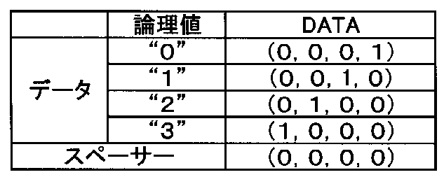
図8は、送信器2の出力部2Bの回路図である。出力部2Bは、ERR_ACK信号が入力される電流受信回路16と、ACK信号が入力される電流受信回路17と、電流受信回路16,17の出力が入力されるOR回路18とから構成されている。電流受信回路16は、カレントミラー回路14と、カレントミラー回路14に接続されるインバータ15とから構成されている。電流受信回路17も電流受信回路16と同様に構成されている。
図9は、受信器4中の復号器7の回路図である。復号器7はDATA信号及びERR_DATA信号が入力される検知器19と、この検知器19の出力であるOut#data信号と故障モード信号とが入力されるAND回路7aと、このAND回路7aの出力と検知器19の出力であるOut#err信号が入力されるマルチプレクサ7bと、マルチプレクサ7bの出力が入力されるC素子7cとから構成されている。
図10は、C素子7cの動作を説明する図であり、それぞれ(a)はC素子7cの構成を示す回路図、(b)はC素子7cの動作の真理値表を示している。図10(a)に示すように、C素子7cは、非同期式の回路に使用される双安定の記憶素子であり、待ち合わせ回路や合流回路とも呼ばれている。
図10(b)に示すように、全ての入力が論理"1"になると出力が論理"1"になり、全ての入力が論理"0"になると出力が論理"0"になる。入力に論理"1"と"0"が混在した状態では、直前の出力を維持する。
図10(b)に示すように、全ての入力が論理"1"になると出力が論理"1"になり、全ての入力が論理"0"になると出力が論理"0"になる。入力に論理"1"と"0"が混在した状態では、直前の出力を維持する。
図11は、復号器7中の検知器19の回路図である。検知器19は、4つの電流検知器19a,19b,19c,19dから構成されている。電流検知器19a~19dのそれぞれは、DATA信号が入力されるカレントミラー回路14と、カレントミラー回路14の出力に接続されるインバータ15と、から構成されている。ERR_DATA信号が入力される電流検知器19eも、上記電流検知器19aと同様の構成である。
図11に示すように、電流検知器19aでは電流Ioutが電圧Voutに変換される。正常モードでは、DATA信号とOUT信号の符号は同じである。
一度配線故障が生じると、ERR_DATA信号は"1"となる。"1"は、「故障」を意味する。これにより、モードは故障モードに遷移する。
故障モードでは、復旧符号が送信器2から送信されたとき、復旧符号は受信器4に記憶される。この記憶データはモードを構成モードに遷移させる。
図9のマルチプレクサ7bからなる出力セレクタでは、(DATA,ERR_DATA)とOUTとの間の接続は、復旧符号に基づいて配線3cの内、オープン故障を有している配線3cを排除するように再構成される。それからデータは、DATA,ERR_DATAを通過する1-of-5符号によって送信される。そして、モードは復旧モードに遷移する。
一度配線故障が生じると、ERR_DATA信号は"1"となる。"1"は、「故障」を意味する。これにより、モードは故障モードに遷移する。
故障モードでは、復旧符号が送信器2から送信されたとき、復旧符号は受信器4に記憶される。この記憶データはモードを構成モードに遷移させる。
図9のマルチプレクサ7bからなる出力セレクタでは、(DATA,ERR_DATA)とOUTとの間の接続は、復旧符号に基づいて配線3cの内、オープン故障を有している配線3cを排除するように再構成される。それからデータは、DATA,ERR_DATAを通過する1-of-5符号によって送信される。そして、モードは復旧モードに遷移する。
図12は、受信器4の出力制御部8の回路図である。出力制御部8は、復号器7からの信号がパストランジスタ8aを介して入力される第1の非同期RSラッチ8bと、第2の非同期RSラッチ8cと、3個のAND回路8d,8e,8fと、5個のOR回路と8g,8h,8i,8j,8kと、から構成されている。
図13は、受信器4の入力部4Bの回路図である。入力部4Bは、Ack#internalに接続される二つのAND回路25と、第1のAND回路25aの出力に接続されるインバータ13と、インバータ13に接続される電流源12と、第2のAND回路25bの出力に接続される電流検知器19fとから構成されている。
図14は、DATA BLOCKとACK BLOCKのモードを示す図であり、(a)は、DATA BLOCKの4モード、(b)は、ACK BLOCKブロックの2モードを示している。
図14(a)に示すように、DATA BLOCKでは、DATA BLOCKの信号の送信及び受信に使用される配線3cの状態によって、正常モード(NORMAL)、故障モード(FAULT)、構成モード(CONFIG)及び復旧モード(RECOVERY)の四つの動作を行う。
図14(b)に示すように、ACK BLOCKでは、ACK BLOCKの信号の送信及び受信に使用される配線3cの状態によって、正常モード(NORMAL)と、復旧モード(RECOVERY)の動作を行う。
図14(a)に示すように、DATA BLOCKでは、DATA BLOCKの信号の送信及び受信に使用される配線3cの状態によって、正常モード(NORMAL)、故障モード(FAULT)、構成モード(CONFIG)及び復旧モード(RECOVERY)の四つの動作を行う。
図14(b)に示すように、ACK BLOCKでは、ACK BLOCKの信号の送信及び受信に使用される配線3cの状態によって、正常モード(NORMAL)と、復旧モード(RECOVERY)の動作を行う。
通信リンクでは、4相符号を使用している。送信器2と受信器4との間のデータ伝送は、電流モードの信号で行い、他の回路は電圧モードの信号を使用している。
図15は、故障から復旧するシステムのタイミングチャートである。この例では、配線3cの内、データ"3"に関連する一つの配線3cはオープンである。最初に、DATA BLOCKとACK BLOCKとは、正常モードで動作している。
最初にDATA BLOCKのモードについて説明する。
正常モードでは、非同期データ転送装置1における通信リンク(非特許文献14参照)と同様に、1-of-4符号に基づいて動作している。
正常モードでは、非同期データ転送装置1における通信リンク(非特許文献14参照)と同様に、1-of-4符号に基づいて動作している。
最初に、データ"0"として(0,0,0,1)が送信器2から受信器4へ送信される。
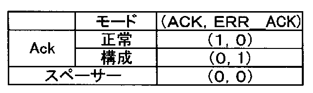
2番目に、受信器4はデータ"0"を検出し、そしてデータ"0"の受信に対してACK信号として(1,0)を送信器2に送信する。
2番目に、受信器4はデータ"0"を検出し、そしてデータ"0"の受信に対してACK信号として(1,0)を送信器2に送信する。
ここで、表3は、ACK BLOCK用の2線符号を示している。
3番目に、送信器2はACK信号を検出し、そしてスペーサーとして(0,0,0,0)を受信器4に送信する。
4番目に、受信器4はスペーサーを検出し、そしてスペーサーとして(0,0)を送信器2に送信する。このようにして、4相プロトコルでは、1通信当たり4ステップが必要となる。DATA BLOCKでは、4相方式のプロトコルを用いている。
4番目に、受信器4はスペーサーを検出し、そしてスペーサーとして(0,0)を送信器2に送信する。このようにして、4相プロトコルでは、1通信当たり4ステップが必要となる。DATA BLOCKでは、4相方式のプロトコルを用いている。
データ"3"が送信されたとき、配線故障は送信器2中の符号器5で検出される。これにより、送信器2のモードは故障モードに遷移する。
表4は故障モード中のDATA BLOCK用の1線符号を示している。ERR_DATA信号は、1ビットの符号語(コードワード)で表されている。

送信器2は故障情報として故障情報(Fault)を受信器4に送信する。故障符号が生成されると送信器2は故障モードに変化する。一方、DATA信号は(0,0,0,0)から変化しない。同時に、復旧符号は故障符号に基づいて生成される。
受信器4が故障情報(Fault)を検出すると、受信器4のモードは故障モードに遷移し、次のモードである構成モードで復旧符号を受信する準備が整う。それから、送信器2のモードは復旧モードに遷移する。
受信器4が故障情報(Fault)を検出すると、受信器4のモードは故障モードに遷移し、次のモードである構成モードで復旧符号を受信する準備が整う。それから、送信器2のモードは復旧モードに遷移する。
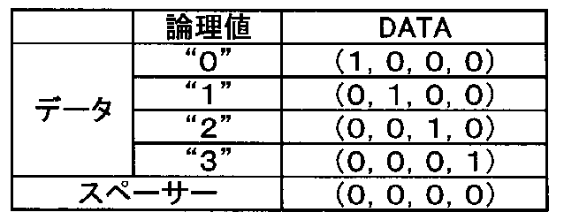
表5は、構成モード中のDATA BLOCK用の1-of-4符号を示している。
復旧符号は、オープン故障を有している配線3cを排除するために生成される。送信器2が復旧符号"3"として(0,0,0,1)を受信器4へ送信した場合、受信器4は、既に故障モードにおいて故障情報を受信しているので、(0,0,0,1)を復旧符号"3"として認識する。
復旧符号は、オープン故障を有している配線3cを排除するために生成される。送信器2が復旧符号"3"として(0,0,0,1)を受信器4へ送信した場合、受信器4は、既に故障モードにおいて故障情報を受信しているので、(0,0,0,1)を復旧符号"3"として認識する。
受信器4が構成モードに変化すると、データ"3"に関係するオープン配線3cは、ERR_DATA信号の配線3cによって置き換えられる。受信器4は、構成モードにおいて、復旧符号に基づいて配線故障を有している配線を正常な配線に置き換える。最後に、送信器2のモードは、復旧モードに遷移する。
表6は、復旧モード中におけるDATA BLOCK用の1-of-5符号を示している。
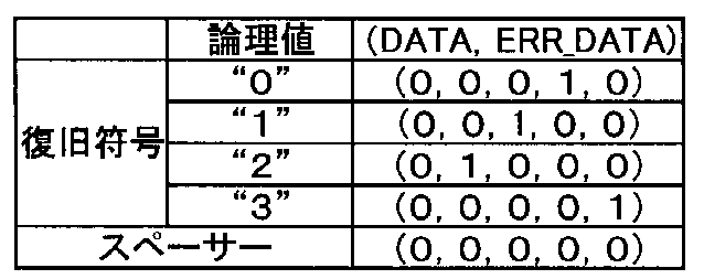
送信器2は、データ"3"として(0,0,0,0,1)を受信器4に送信する。
受信器4は、データ"3"として(0,0,0,0,1)を認識し、その結果、復旧モードで動作する。これにより、データ"3"に関係する配線故障下でデータ転送を行う復旧モードで動作する。
受信器4は、データ"3"として(0,0,0,0,1)を認識し、その結果、復旧モードで動作する。これにより、データ"3"に関係する配線故障下でデータ転送を行う復旧モードで動作する。
モードが構成モードに遷移するとき、符号器5の出力は復旧符号となる。復旧符号は故障の無い配線3cを使用して生成されるので、故障符号は(0,0,0,0)に戻る。
図3の第1のAND回路5a及び第2のAND回路5bからなる入力セレクタでは、(DATA,ERR_DATA)とINとの間の接続は、復旧符号に基づいて配線3cの内オープン故障を有している一つの配線を排除するように再構成される。
モードが復旧モードに遷移するとき、DATA信号及びERR_DATA信号のデータは1-of-5符号によって送信される。復旧モードにおいて、送信器2から受信器4への信号、例えばERR_DATA信号は、配線故障を有している配線を正常な配線に置き換えて送信される。
図3の第1のAND回路5a及び第2のAND回路5bからなる入力セレクタでは、(DATA,ERR_DATA)とINとの間の接続は、復旧符号に基づいて配線3cの内オープン故障を有している一つの配線を排除するように再構成される。
モードが復旧モードに遷移するとき、DATA信号及びERR_DATA信号のデータは1-of-5符号によって送信される。復旧モードにおいて、送信器2から受信器4への信号、例えばERR_DATA信号は、配線故障を有している配線を正常な配線に置き換えて送信される。
次に、ACK BLOCKのモードについて説明する。
ACK信号に対して、故障-復旧系のモードは、図14(b)に示すように遷移する。
第一に、ACK信号は正常モードで動作している。
ACK BLOCKの配線故障が受信器4の入力部4Bで検出されたときには、ACK BLOCKの2線符号は、表3に示すように(1,0)から(0,1)に変化する。
復旧モードでは、送信器2の出力部2Bはどのモードでも2線符号の論理和によってAcknowledgement情報を検出することで、Acknowledgement情報はACK BLOCKの配線故障下で受信される。Acknowledgement情報は、確認情報とも呼ばれている。
ACK信号に対して、故障-復旧系のモードは、図14(b)に示すように遷移する。
第一に、ACK信号は正常モードで動作している。
ACK BLOCKの配線故障が受信器4の入力部4Bで検出されたときには、ACK BLOCKの2線符号は、表3に示すように(1,0)から(0,1)に変化する。
復旧モードでは、送信器2の出力部2Bはどのモードでも2線符号の論理和によってAcknowledgement情報を検出することで、Acknowledgement情報はACK BLOCKの配線故障下で受信される。Acknowledgement情報は、確認情報とも呼ばれている。
送信器2の入力制御部6の動作について、纏めて説明する。
(正常モード)
符号器5の電流ドライバ11a~11dでオープン故障が検出されると、故障符号が生成され、入力制御部6に送出される。故障符号は、表2に示す符号と同じである。この故障符号は図7に示す入力制御部6の非同期RSラッチ6gに入力される。
(故障モード)
符号器5の電流ドライバでオープン故障が検出されると、故障符号に対応した4線の内の1線が高(high)となることで、故障符号が生成される。これにより、表4のERR_DATA信号に対応する故障情報(Fault)が生成される。
(構成モード)
符号器5の故障符号が低(low)になると同時に、CONFIG MODE信号を高(high)にする(図3のCONFIG MODE信号を参照)。
次に、表5に示す復旧符号を生成する。
(復旧モード)
CONFIG MODE信号をlowにすると同時に、RECOVERY MODE信号を高(high)にする(図3のRECOVERY MODE信号を参照)。
次に受信器4の出力制御部8の動作について、纏めて説明する。
(正常モード)
送信器2から表4のFaultが転送されてくると、Fault(Out#err)が高(high)になる。この信号は、図12に示す受信器4の出力制御部8で受信し、非同期RSラッチ8bに入力される。
(故障モード)
図12におけるFAULT MODE信号を高(high)にする。
(構成モード)
図12において、表5の復旧符号であるRecovery codeによってOut#data信号が、送信器2から送信されてくると、受信器4の出力制御部8で受信され、第2の非同期RSラッチ8cに保存される。
(復旧モード)
図12のRECOVERY MODE信号を高(high)にする。
(正常モード)
送信器2から表4のFaultが転送されてくると、Fault(Out#err)が高(high)になる。この信号は、図12に示す受信器4の出力制御部8で受信し、非同期RSラッチ8bに入力される。
(故障モード)
図12におけるFAULT MODE信号を高(high)にする。
(構成モード)
図12において、表5の復旧符号であるRecovery codeによってOut#data信号が、送信器2から送信されてくると、受信器4の出力制御部8で受信され、第2の非同期RSラッチ8cに保存される。
(復旧モード)
図12のRECOVERY MODE信号を高(high)にする。
以上、説明したように、本発明の非同期データ転送装置1によれば、電流量の監視に基づく配線のオープン(永久)故障の検出を実現することができる。つまり、データ転送時に入力電流を受信側への「データ転送電流」Iwと、監視用の「フィードバック電流」Idに分流を行う。この2つの電流量の合計値は一定なため、配線故障時は「データ転送電流」Iwがカットオフされる一方で、「フィードバック電流」Idは単調に増加する。「フィードバック電流」Idの増加を送信側で検出することで、遅延仮定なしに配線故障が検出可能になる。検出した故障配線を予備の正常な配線3cと入れ替えることで、非同期データ転送装置1としての機能が回復する。
これにより、本発明の非同期データ転送装置1では、QDI論理型の非同期データ転送の遅延故障耐性を有しながら、配線故障耐性を実現することが可能となる。
これにより、本発明の非同期データ転送装置1では、QDI論理型の非同期データ転送の遅延故障耐性を有しながら、配線故障耐性を実現することが可能となる。
本発明の非同期データ転送装置1の機能を表7に示す。表7には、表1の従来の非同期データ転送装置の機能も示している。表7に示すように、本発明の非同期データ転送装置1では、従来できなかった入力ポートでの配線故障監視と検知とをQDI論理型で行うことができる。
以下、本発明を実施例によりさらに詳細に説明する。
本発明の非同期データ転送装置1の回路をSilterra社の0.13μmのCMOS技術で作成し、HSPICEで評価した。送信器2と受信器4との間の配線3cの長さは1mmである。配線3cはパイモデルでシミュレーションした。パイモデルのパラメータとして、抵抗は91Ω/mmとし、容量は84fF/mmとした。
本発明の非同期データ転送装置1の回路をSilterra社の0.13μmのCMOS技術で作成し、HSPICEで評価した。送信器2と受信器4との間の配線3cの長さは1mmである。配線3cはパイモデルでシミュレーションした。パイモデルのパラメータとして、抵抗は91Ω/mmとし、容量は84fF/mmとした。
図16は、シミュレーションのタイミングチャートである。図16では、配線3cがData"3"の故障の場合を示す。Iinは165μAとした。
図16に示すように、DATA信号がオープン故障を有する配線3cを介して送信されるとき、Idが大きくなる。このIdが通信リンクを復旧するように故障モードに遷移する。
図16に示すように、DATA信号がオープン故障を有する配線3cを介して送信されるとき、Idが大きくなる。このIdが通信リンクを復旧するように故障モードに遷移する。
表8は、本発明を比較例と対比した表である。
表8に示すように、本発明の場合には、配線故障検出と配線故障下での動作補正、つまり復旧が可能である。また、遅延時間に不感であるQDI論理型に対応している。配線数はnビットに対して2n+3であり、使用したトランジスタ数は1280個であった。スループットは837Mbps、消費電力は584μW、エネルギーは698fJ/bitであった。

表8に示すように、本発明の場合には、配線故障検出と配線故障下での動作補正、つまり復旧が可能である。また、遅延時間に不感であるQDI論理型に対応している。配線数はnビットに対して2n+3であり、使用したトランジスタ数は1280個であった。スループットは837Mbps、消費電力は584μW、エネルギーは698fJ/bitであった。
一方、1-of-4符号による従来例(非特許文献9参照)では、QDI論理型には対応しているが、配線故障検出と配線故障下での動作補正ができない。配線数はnビットに対して2n+1であり、使用したトランジスタ数は545個であった。スループットは840Mbps、消費電力は328μW、エネルギーは388fJ/bitであった。
一方、二重化した1-of-4符号による従来例(非特許文献10参照)では、QDI論理型には対応していないが、配線故障検出はできるが、配線故障下での動作補正ができないものである。配線数はnビットに対して2×(2n+1)であり、使用したトランジスタ数は1049個であった。スループットは741Mbps、消費電力は616μW、エネルギーは831fJ/bitであった。
一方、三重化した1-of-4符号による従来例(非特許文献11参照)では、QDI論理型には対応していないが、本発明と同様に配線故障検出と配線故障下での動作補正、つまり復旧が可能である。配線数はnビットに対して3×(2n+1)であり、使用したトランジスタ数は1223個であった。スループットは622Mbps、消費電力は761μW、エネルギーは1223fJ/bitであった。
上記の結果から、本発明の遅延及び配線故障耐性を有する非同期データ転送装置1は、遅延時間に不感であるQDI論理型に対応し、配線故障の検出と故障した配線の復旧が可能である。また、本発明の非同期データ転送装置1の使用トランジスタ数は、比較例2と比較例3との間の数であるが、スループットは、比較例1と同様に高速である。またその消費電力は、比較例2及び3よりも低くなった。また、nビットへ拡張した場合でも入力制御部6及び出力制御部8はビット幅に依存しないことから、トランジスタ数は比較例2及び比較例3よりも小さくなる。
本発明の非同期データ転送装置1を使用したネットワークオンチップは、プロセス、電源電圧、温度変動に伴う遅延変動耐性を有するだけでなく、LSI20の経年劣化に伴う配線故障耐性をも有しているので、信頼性の高いシステムを実現できる。このため、過酷な環境下での使用が見込まれる車載用及び宇宙用のシステムオンチップ(SoC)に用いることができる。第4世代の携帯電話等にも応用できる。
本発明の非同期データ転送装置1はクロック信号を用いない非同期式であることから、クロック信号を生成する回路の削除に伴う電力の削減も可能であるために、システムの低電力化も可能である。
本発明は、上記実施の形態に限定されるものではなく、特許請求の範囲に記載した発明の範囲内で種々の変形が可能であり、それらも本発明の範囲内に含まれることはいうまでもない。
Claims (8)
- IPコア間に配設されるLSIの非同期データ転送装置において、
第1のIPコアに接続される第1の配線と、
第2のIPコアに接続される第2の配線と、
上記第1の配線に接続される送信器と、
上記第2の配線に接続される受信器と、
上記送信器と上記受信器とを接続する第3の配線と、を含み、
上記送信器は、符号器と入力制御部とを有している入力部と、出力部と、を含み、
上記送信器の符号器は、上記第3の配線のオープン故障を検出する電流ドライバ回路を備えていることを特徴とする、非同期データ転送装置。 - 前記受信器は、入力部と、復号器と出力制御部とを有している出力部と、を含んでいることを特徴とする、請求項1に記載の非同期データ転送装置。
- 前記送信器及び受信器は、擬似遅延不感の論理方式の動作を行なうことを特徴とする、請求項1又は2に記載の非同期データ転送装置。
- 前記符号器は、電流源と、該電流源に接続されるインバータと、該インバータに接続されるカレントミラー回路と、該カレントミラー回路に接続されるインバータと、を含んで構成されることを特徴とする、請求項1に記載の非同期データ転送装置。
- 前記復号器は、カレントミラー回路と、該カレントミラー回路に接続されるインバータと、を含んで構成されることを特徴とする、請求項2に記載の非同期データ転送装置。
- 前記送信器の入力部にはIN信号が入力され、該入力部から前記受信器にDATA信号及びERR_DATA信号が出力され、前記受信器の出力部からOUT信号が出力されることを特徴とする、請求項1に記載の非同期データ転送装置。
- 前記IN信号、前記DATA信号、前記ERR_DATA信号、及び前記OUT信号によりDATA BLOCKが構成され、該DATA BLOCKは、正常モード、故障モード、構成モード及び復旧モードの動作を行うことを特徴とする、請求項6に記載の非同期データ転送装置。
- 前記正常モードにおいて、配線故障を前記符号器で検出して、前記送信器は前記故障モードに遷移し、
前記故障モードでは、前記送信器は故障情報を前記受信器に送信し、同時に復旧符号を故障符号に基づいて生成し、前記受信器は故障モードに遷移し、
前記送信器は、上記復旧符号に基づいて前記構成モードに遷移し、該送信器が上記復旧符号を受信器に送信すると、該受信器が前記構成モードに遷移し、
前記送信器は、前記構成モードにおいて、上記復旧符号に基づいて配線故障を有している配線を排除するように再構成され、該送信器は、復旧モードに遷移し、
前記受信器は、前記構成モードにおいて、前記送信器からの信号によって復旧モードに遷移し、
前記復旧モードにおいて、前記送信器から前記受信器への信号は、前記配線故障を有している配線を正常な配線に置き換えて送信されることを特徴とする、請求項6又は7に記載の非同期データ転送装置。
Applications Claiming Priority (2)
| Application Number | Priority Date | Filing Date | Title |
|---|---|---|---|
| JP2011054861A JP2012191531A (ja) | 2011-03-12 | 2011-03-12 | 非同期データ転送装置 |
| JP2011-054861 | 2011-03-12 |
Publications (1)
| Publication Number | Publication Date |
|---|---|
| WO2012124606A1 true WO2012124606A1 (ja) | 2012-09-20 |
Family
ID=46830679
Family Applications (1)
| Application Number | Title | Priority Date | Filing Date |
|---|---|---|---|
| PCT/JP2012/055990 Ceased WO2012124606A1 (ja) | 2011-03-12 | 2012-03-08 | 非同期データ転送装置 |
Country Status (3)
| Country | Link |
|---|---|
| JP (1) | JP2012191531A (ja) |
| TW (1) | TW201246514A (ja) |
| WO (1) | WO2012124606A1 (ja) |
Families Citing this family (1)
| Publication number | Priority date | Publication date | Assignee | Title |
|---|---|---|---|---|
| TWI841454B (zh) * | 2023-07-21 | 2024-05-01 | 乾瞻科技股份有限公司 | 適用於裸片對裸片的連接介面及其線道連接方法 |
Citations (1)
| Publication number | Priority date | Publication date | Assignee | Title |
|---|---|---|---|---|
| JP2007501550A (ja) * | 2003-08-06 | 2007-01-25 | ローベルト ボッシュ ゲゼルシャフト ミット ベシュレンクテル ハフツング | 双方向のシングルワイヤデータ伝送方法および装置 |
-
2011
- 2011-03-12 JP JP2011054861A patent/JP2012191531A/ja not_active Withdrawn
-
2012
- 2012-03-08 WO PCT/JP2012/055990 patent/WO2012124606A1/ja not_active Ceased
- 2012-03-12 TW TW101108260A patent/TW201246514A/zh unknown
Patent Citations (1)
| Publication number | Priority date | Publication date | Assignee | Title |
|---|---|---|---|---|
| JP2007501550A (ja) * | 2003-08-06 | 2007-01-25 | ローベルト ボッシュ ゲゼルシャフト ミット ベシュレンクテル ハフツング | 双方向のシングルワイヤデータ伝送方法および装置 |
Non-Patent Citations (1)
| Title |
|---|
| BENINI, L. ET AL.: "Networks on chips: a new SoC paradigm", COMPUTER, vol. 35, no. 1, January 2002 (2002-01-01), pages 70 - 78 * |
Also Published As
| Publication number | Publication date |
|---|---|
| TW201246514A (en) | 2012-11-16 |
| JP2012191531A (ja) | 2012-10-04 |
Similar Documents
| Publication | Publication Date | Title |
|---|---|---|
| Raghunathan et al. | A survey of techniques for energy efficient on-chip communication | |
| Bertozzi et al. | Xpipes: A network-on-chip architecture for gigascale systems-on-chip | |
| Tsai et al. | A fault-tolerant NoC scheme using bidirectional channel | |
| Hosseini et al. | Expression of Concern: A fault-aware dynamic routing algorithm for on-chip networks | |
| Frantz et al. | Dependable network-on-chip router able to simultaneously tolerate soft errors and crosstalk | |
| Tamhankar et al. | Performance driven reliable link design for networks on chips | |
| Rossi et al. | Power consumption of fault tolerant busses | |
| Zonouz et al. | A fault tolerant NoC architecture for reliability improvement and latency reduction | |
| Tamhankar et al. | Timing-error-tolerant network-on-chip design methodology | |
| JP2012191531A (ja) | 非同期データ転送装置 | |
| Nunez-Yanez et al. | Adaptive routing strategies for fault-tolerant on-chip networks in dynamically reconfigurable systems | |
| Karimi | Online network-on-chip switch fault detection and diagnosis using functional switch faults | |
| Neishaburi et al. | ERAVC: Enhanced reliability aware NoC router | |
| CN102904807A (zh) | 一种通过数据分割传输实现容错可重构片上网络的方法 | |
| Louis et al. | Reliable router architecture with elastic buffer for NoC architecture | |
| Siddagangappa | Asynchronous NoC with fault tolerant mechanism: a comprehensive review | |
| Pasca et al. | Configurable serial fault-tolerant link for communication in 3D integrated systems | |
| De Micheli | Designing robust systems with uncertain information | |
| Xiangming et al. | Configurable redundant routing for network on chip | |
| JP2017208736A (ja) | ネットワークオンチップ用の欠陥耐性ルータ | |
| Satish et al. | Faulty Node Detection and Correction of Route in Network-On-Chip (NoC) | |
| Yoneda et al. | Network-on-Chip based multiple-core centralized ECUs for safety-critical automotive applications | |
| Patooghy et al. | A low-overhead and reliable switch architecture for Network-on-Chips | |
| Dumitras et al. | Enabling on-chip diversity through architectural communication design | |
| Shirmohammadi et al. | ReNo: novel switch architecture for reliability improvement of NoCs |
Legal Events
| Date | Code | Title | Description |
|---|---|---|---|
| 121 | Ep: the epo has been informed by wipo that ep was designated in this application |
Ref document number: 12758079 Country of ref document: EP Kind code of ref document: A1 |
|
| DPE1 | Request for preliminary examination filed after expiration of 19th month from priority date (pct application filed from 20040101) | ||
| NENP | Non-entry into the national phase |
Ref country code: DE |
|
| 122 | Ep: pct application non-entry in european phase |
Ref document number: 12758079 Country of ref document: EP Kind code of ref document: A1 |