WO2012117928A1 - タッチパネル付き表示装置及びその駆動方法 - Google Patents
タッチパネル付き表示装置及びその駆動方法 Download PDFInfo
- Publication number
- WO2012117928A1 WO2012117928A1 PCT/JP2012/054380 JP2012054380W WO2012117928A1 WO 2012117928 A1 WO2012117928 A1 WO 2012117928A1 JP 2012054380 W JP2012054380 W JP 2012054380W WO 2012117928 A1 WO2012117928 A1 WO 2012117928A1
- Authority
- WO
- WIPO (PCT)
- Prior art keywords
- touch panel
- display device
- voltage
- liquid crystal
- panel
- Prior art date
- Legal status (The legal status is an assumption and is not a legal conclusion. Google has not performed a legal analysis and makes no representation as to the accuracy of the status listed.)
- Ceased
Links
Images







Classifications
-
- G—PHYSICS
- G06—COMPUTING OR CALCULATING; COUNTING
- G06F—ELECTRIC DIGITAL DATA PROCESSING
- G06F3/00—Input arrangements for transferring data to be processed into a form capable of being handled by the computer; Output arrangements for transferring data from processing unit to output unit, e.g. interface arrangements
- G06F3/01—Input arrangements or combined input and output arrangements for interaction between user and computer
- G06F3/03—Arrangements for converting the position or the displacement of a member into a coded form
- G06F3/041—Digitisers, e.g. for touch screens or touch pads, characterised by the transducing means
- G06F3/044—Digitisers, e.g. for touch screens or touch pads, characterised by the transducing means by capacitive means
- G06F3/0446—Digitisers, e.g. for touch screens or touch pads, characterised by the transducing means by capacitive means using a grid-like structure of electrodes in at least two directions, e.g. using row and column electrodes
-
- G—PHYSICS
- G06—COMPUTING OR CALCULATING; COUNTING
- G06F—ELECTRIC DIGITAL DATA PROCESSING
- G06F3/00—Input arrangements for transferring data to be processed into a form capable of being handled by the computer; Output arrangements for transferring data from processing unit to output unit, e.g. interface arrangements
- G06F3/01—Input arrangements or combined input and output arrangements for interaction between user and computer
- G06F3/03—Arrangements for converting the position or the displacement of a member into a coded form
- G06F3/041—Digitisers, e.g. for touch screens or touch pads, characterised by the transducing means
- G06F3/0412—Digitisers structurally integrated in a display
-
- G—PHYSICS
- G06—COMPUTING OR CALCULATING; COUNTING
- G06F—ELECTRIC DIGITAL DATA PROCESSING
- G06F3/00—Input arrangements for transferring data to be processed into a form capable of being handled by the computer; Output arrangements for transferring data from processing unit to output unit, e.g. interface arrangements
- G06F3/01—Input arrangements or combined input and output arrangements for interaction between user and computer
- G06F3/03—Arrangements for converting the position or the displacement of a member into a coded form
- G06F3/041—Digitisers, e.g. for touch screens or touch pads, characterised by the transducing means
- G06F3/0416—Control or interface arrangements specially adapted for digitisers
- G06F3/04166—Details of scanning methods, e.g. sampling time, grouping of sub areas or time sharing with display driving
-
- G—PHYSICS
- G06—COMPUTING OR CALCULATING; COUNTING
- G06F—ELECTRIC DIGITAL DATA PROCESSING
- G06F3/00—Input arrangements for transferring data to be processed into a form capable of being handled by the computer; Output arrangements for transferring data from processing unit to output unit, e.g. interface arrangements
- G06F3/01—Input arrangements or combined input and output arrangements for interaction between user and computer
- G06F3/03—Arrangements for converting the position or the displacement of a member into a coded form
- G06F3/041—Digitisers, e.g. for touch screens or touch pads, characterised by the transducing means
- G06F3/0416—Control or interface arrangements specially adapted for digitisers
- G06F3/0418—Control or interface arrangements specially adapted for digitisers for error correction or compensation, e.g. based on parallax, calibration or alignment
-
- G—PHYSICS
- G06—COMPUTING OR CALCULATING; COUNTING
- G06F—ELECTRIC DIGITAL DATA PROCESSING
- G06F3/00—Input arrangements for transferring data to be processed into a form capable of being handled by the computer; Output arrangements for transferring data from processing unit to output unit, e.g. interface arrangements
- G06F3/01—Input arrangements or combined input and output arrangements for interaction between user and computer
- G06F3/03—Arrangements for converting the position or the displacement of a member into a coded form
- G06F3/041—Digitisers, e.g. for touch screens or touch pads, characterised by the transducing means
- G06F3/0416—Control or interface arrangements specially adapted for digitisers
- G06F3/0418—Control or interface arrangements specially adapted for digitisers for error correction or compensation, e.g. based on parallax, calibration or alignment
- G06F3/04184—Synchronisation with the driving of the display or the backlighting unit to avoid interferences generated internally
-
- G—PHYSICS
- G06—COMPUTING OR CALCULATING; COUNTING
- G06F—ELECTRIC DIGITAL DATA PROCESSING
- G06F3/00—Input arrangements for transferring data to be processed into a form capable of being handled by the computer; Output arrangements for transferring data from processing unit to output unit, e.g. interface arrangements
- G06F3/01—Input arrangements or combined input and output arrangements for interaction between user and computer
- G06F3/03—Arrangements for converting the position or the displacement of a member into a coded form
- G06F3/041—Digitisers, e.g. for touch screens or touch pads, characterised by the transducing means
- G06F3/044—Digitisers, e.g. for touch screens or touch pads, characterised by the transducing means by capacitive means
-
- G—PHYSICS
- G06—COMPUTING OR CALCULATING; COUNTING
- G06F—ELECTRIC DIGITAL DATA PROCESSING
- G06F2203/00—Indexing scheme relating to G06F3/00 - G06F3/048
- G06F2203/041—Indexing scheme relating to G06F3/041 - G06F3/045
- G06F2203/04112—Electrode mesh in capacitive digitiser: electrode for touch sensing is formed of a mesh of very fine, normally metallic, interconnected lines that are almost invisible to see. This provides a quite large but transparent electrode surface, without need for ITO or similar transparent conductive material
Definitions
- the present invention relates to a display device having a capacitive touch panel and a driving method thereof.
- the capacitive touch panel obtains a detection output based on the capacitance difference between the electrodes when the finger is not in contact and when the finger is in contact.
- FIG. 19 is a cross-sectional view showing a schematic configuration of a conventional liquid crystal display device with a capacitive touch panel.
- a conventional liquid crystal display device 100 is configured by laminating a liquid crystal panel (LCD: Liquid Crystal Display) 100, a touch panel (TP: Touch Panel) 200, and a cover glass 300 in this order.
- the touch panel 200 is disposed on the liquid crystal panel 100 through an air gap.
- a touch panel integrated with a liquid crystal display device is arranged with no air gap between the touch panel and the distance between the touch functional layer of the touch panel and the liquid crystal panel. Getting closer.
- the capacitive touch panel When the capacitive touch panel is integrated (in-cell) as described above, it is strongly affected by noise generated by the liquid crystal panel. That is, when the touch panel performs a detection operation while the liquid crystal panel performs display, radiation noise generated from the liquid crystal panel adversely affects the detection sensitivity of the touch panel. Therefore, in order to prevent the performance of the capacitive touch panel from deteriorating, a technology for reducing the influence of noise from the liquid crystal panel has been developed.
- the touch panel is driven by driving the touch panel during a period in which the liquid crystal panel is not performing display driving (period in which display between frames is not performed).
- the noise received from the LCD panel is reduced.
- Non-Patent Document 1 since it is necessary to secure a display period (about 14 ms) for one frame, there is an upper limit on the sensing time of the touch panel. For this reason, the signal which a touch panel detects falls, and the performance of a touch panel cannot be improved effectively.
- the touch panel is driven using a period in which display between frames is not performed. Therefore, the frequency of coordinate output on the touch panel is limited to 60 Hz.
- the frequency of coordinate output requires 180 Hz to 240 Hz or more. The technique disclosed in Non-Patent Document 1 cannot cope with such high-speed driving of the touch panel.
- the present invention has been made in view of the above problems, and an object of the present invention is to provide a display device with a touch panel that improves the detection accuracy by suppressing the influence of noise without limiting the frequency of coordinate output in the touch panel. There is to do.
- the present inventors diligently studied to solve the above-mentioned problem, and found that in the display panel of the display device, radiation noise is generated at the moment when the voltage supplied to the data signal line is changed.
- a display device with a touch panel is arranged on the surface of an observer side of the display panel and the display panel or provided inside the display panel in order to solve the above-described problem.
- a display device with a touch panel comprising a capacitive touch panel,
- the display panel is A plurality of data signal lines and a plurality of scanning signal lines orthogonal to each other;
- a data signal line driving circuit for sequentially supplying a voltage to each of the plurality of data signal lines,
- the touch panel A plurality of transmitting electrodes and a plurality of receiving electrodes orthogonal to each other;
- An integration circuit A switching element that connects any one of the plurality of receiving electrodes and the integrating circuit;
- Control means for switching on and off of the switching element at least once while a voltage is supplied to the plurality of data signal lines,
- the control means is characterized in that the switching element is kept on or off for a certain period from the moment when the data signal line driving circuit changes the voltage.
- the touch panel when the voltage supplied to the transmission electrode changes in the touch panel, electric charge flows from the reception electrode. At this time, the switching element is in an ON state, and the receiving electrode and the integrating circuit are connected.
- the touch panel can perform touch detection by integrating the electric charge flowing from the receiving electrode by the integration circuit.
- the switching element can be switched on and off at least once while the data signal line driving circuit supplies a voltage for display to the data signal line. That is, the touch panel performs driving for touch detection during a display period of the display panel.
- the switching element is kept on or off for a certain period from the moment when the voltage of the data signal line changes.
- the switching element when the switching element is kept in the off state for a certain period of time, the receiving electrode and the integrating circuit are disconnected while noise is generated. Therefore, the integration circuit can avoid being affected by radiation noise.
- the integration circuit integrates the electric charge flowing from the receiving electrode before and after the generation of noise. For this reason, the potential amplitude V noise of the noise source between the start of integration and the end of integration becomes zero.
- the noise amount Q noise affecting the integration circuit is determined between the capacitance C sense-LCD formed between the liquid crystal panel and the reception electrode, and the integration start time and the integration end time. Is obtained by the product of the potential amplitude V noise of the noise source. For this reason, if the potential amplitude V noise of the noise source is zero, the noise amount Q noise is zero. Therefore, the integration circuit can integrate the charge flowing from the receiving electrode without being affected by noise.
- the display device with a touch panel sufficiently secures the detection time of the touch panel by driving the touch panel during the display period of the display panel while suppressing the influence of noise. be able to. Thereby, the detection accuracy of the touch panel can be improved.
- the frequency of the output (coordinate output) by the integration circuit is not limited to 60 Hz, it is possible to suitably cope with high-speed input to the touch panel.
- An operation method of a display device with a touch panel includes a display panel and a capacitive touch panel that is disposed on an observer-side surface of the display panel or provided in the display panel
- An operation method of a display device with a touch panel comprising:
- the display panel is A plurality of data signal lines and a plurality of scanning signal lines orthogonal to each other;
- a data signal line driving circuit for sequentially supplying a voltage to each of the plurality of data signal lines,
- the touch panel A plurality of transmitting electrodes and a plurality of receiving electrodes orthogonal to each other;
- An integration circuit A switching element that connects any one of the plurality of receiving electrodes and the integrating circuit;
- Control means for switching on and off of the switching element at least once while a voltage is supplied to the plurality of data signal lines,
- the control means is characterized in that the switching element is kept on or off for a certain period from the moment when the data signal line driving circuit changes the voltage.
- a display device with a touch panel is a display device with a touch panel including a display panel and a capacitance-type touch panel disposed on an observer-side surface of the display panel.
- the panel includes a plurality of data signal lines and a plurality of scanning signal lines orthogonal to each other, and a data signal line driving circuit that sequentially supplies a voltage to each of the plurality of data signal lines
- the touch panel includes: Voltages are supplied to the plurality of transmission electrodes and the plurality of reception electrodes orthogonal to each other, the integration circuit, the switching element connecting any one of the plurality of reception electrodes and the integration circuit, and the plurality of data signal lines.
- Control means for switching on and off the switching element at least once during the operation comprising the data signal A certain period from the moment the drive circuit has changed the voltage, to maintain the on or off state of the switching element, it is possible to suitably improve the detection accuracy of the touch panel.
- FIG. 3 is a timing chart for explaining a basic operation of the liquid crystal panel shown in FIG. 2. It is a timing chart for demonstrating the waveform of the radiation noise generate
- FIG. It is a figure which shows the various voltage waveform at the time of carrying out alternating current drive of the common electrode of a liquid crystal panel. It is a figure which shows the various voltage waveforms at the time of carrying out direct current drive of the common electrode of a liquid crystal panel. It is sectional drawing which shows schematic structure of the conventional liquid crystal display device with an electrostatic capacitance type touch panel.
- FIG. 2 is a cross-sectional view illustrating a schematic configuration of the liquid crystal display device (display device with a touch panel) 1 according to the present embodiment.
- the liquid crystal display device 1 is configured by laminating a liquid crystal panel (LCD: Liquid Crystal Display) 10, a touch panel (TP: Touch Panel) 20, and a cover glass 30 in this order.
- the touch panel 20 is directly disposed on the surface on the viewer side of the liquid crystal panel 10. That is, there is no air gap between the liquid crystal panel 10 and the touch panel 20.
- the touch panel 20 is a capacitive touch panel.
- a capacitance is formed between the finger 2 and the electrode of the touch panel 20.
- the touch panel 20 detects the touch or non-touch of the finger based on the capacitance difference between the electrodes when the finger 2 is not touching and when the finger 2 is touching.
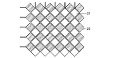
- FIG. 3 is a top view showing an X electrode (transmission electrode; transmission line; drive line) 21 and a Y electrode (reception electrode; reception line; sense line) 22 included in the touch panel 20.
- a plurality of X electrodes 21 are arranged on the substrate of the touch panel 20, and a plurality of Y electrodes are arranged so as to be orthogonal to these.
- Each of the X electrode 21 and the Y electrode 22 is formed in a pattern in which wide portions and narrow portions are alternately arranged along the extending direction.
- FIG. 4 is a diagram showing the processing circuit 40 provided in the touch panel 20.
- the processing circuit 40 includes a signal generator 23 connected to the X electrode 21, a sampling switch 41 connected to the Y electrode 22, an integration circuit 42, an amplifier 43, a reset switch (reset means) 44, A charge cancel circuit 45, a detector 47, and a timing controller 48 are provided.
- the touch panel 20 employs a mutual capacitance method, and the X electrode 21 and the Y electrode 22 are coupled by a capacitor 24.
- a processing circuit 40 shown in FIG. 4 represents a processing circuit for an arbitrary X electrode 21 and Y electrode 22 among the plurality of X electrodes 21 and the plurality of Y electrodes 22 shown in FIG. That is, in this embodiment, it is assumed that a sampling switch 41, an integration circuit 42, an amplifier 43, a reset switch 44, and the like are provided for each of the plurality of Y electrodes 22. Each of the plurality of Y electrodes 22 is connected to each integrating circuit 42 via each sampling switch 41.
- One detector 47 is arranged so as to be connectable to all the integrating circuits 42 arranged in the processing circuit 40. That is, the detector 47 is arranged for each processing circuit 40, in other words, for each Y electrode 22.
- the embodiment of the present invention is not limited to this, and a configuration in which one common detector 47 is arranged for the plurality of Y electrodes 22 may be employed.
- the signal generator 23 outputs a periodic voltage signal to the X electrode.
- a current flows through the Y electrode 22 when the voltage signal supplied to the X electrode changes from the H level to the L level or from the L level to the H level.
- the sampling switch 41 is disposed between the Y electrode 22 and the integration circuit 42.
- the sampling switch 41 When the signal generator 23 changes the voltage signal from the L level to the H level, the sampling switch 41 is turned on by being connected to the terminal “1”. Thereby, the Y electrode 22 and the integrating circuit 42 are connected.
- the signal generator 23 when the signal generator 23 changes the voltage signal from the H level to the L level, the signal generator 23 is in the OFF state because it is connected to the terminal “0”. Thereby, the Y electrode 22 is grounded.
- the reset switch 44 grounds the integrating circuit 42 when it is in the on state, and resets its integrating capacitance.
- the reset switch 44 controls the detection period on the touch panel 20 to a predetermined cycle by switching on and off.
- the output timing of the voltage signal from the signal generator 23 and the on / off timing of the sampling switch 41 and the reset switch 44 are controlled by the timing controller 48.
- the integration circuit 42 includes an operational amplifier and an integration capacitor Cs.
- the integration capacitor Cs accumulates the charge that has flowed to the Y electrode 22 when the sampling switch 41 is on.
- the capacity 24 changes between when the finger is not in contact and when the finger is in contact (the capacity is reduced when the finger is in contact).
- the integrating circuit 42 outputs a voltage proportional to the capacitance difference of the coupling capacitance 24 between the X electrode 21 and the Y electrode 22 by integrating the current value flowing through the Y electrode 22.
- the detector 47 detects the contact or non-contact of the finger by measuring the difference in output voltage by the integration circuit 42.
- the configuration of the processing circuit 40 is not limited to that described above, and the touch panel 20 includes an integration circuit 42, an amplifier 43, and a reset switch 44 that are provided so as to be selectively connected to the plurality of Y electrodes 22. Each may be provided.
- the processing circuit 40 For a detailed configuration of the processing circuit 40, reference can be made to US Pat. No. 6,452,514.
- FIG. 5 is a diagram illustrating an example of a timing chart for explaining the operation of the touch panel 20.
- FIG. 6 is a diagram showing a table summarizing the operation steps of the touch panel 20.
- FIG. 5 shows an example of the timing control signal input to each sampling switch 41 and each reset switch 44 and the output voltage of any integration circuit 42.
- the touch panel 20 repeats the following steps A to F.
- the reset switch 44 is turned off by the timing control signal.
- the integration capacity of the integration circuit 42 is reset to an initial state (for example, 0 V) (step A).
- the sampling switch 41 connects the terminal “1” with the timing control signal while the voltage signal supplied to the X electrode 21 changes from the L level to the H level.
- the Y electrode 22 is connected to the integrating circuit 42 via the terminal “1”.
- the electric charge flowing from the Y electrode 22 is transferred to the integration capacitor of the integration circuit 42 (step C).
- the sampling switch 41 is connected to the terminal “0” by the timing control signal, and the Y electrode 22 is electrically grounded via the terminal “0”.
- the charge in the integrating circuit 42 is held, and a hold state is set (step E).
- Step B and Step D are dead times, and none of the switches and terminals are connected.
- integration is performed at least once by repeating steps B to E at least once in one X electrode 21. Then, when the process of the certain X electrode 21 is finished, a reset process is executed, and then, in the next X electrode 21, Step B to Step E are repeated at least once.
- step C the detector 47 measures the output voltage of the integrating circuit 42 while the sampling switch 41 connects the terminal “0” and maintains the hold state (step F). After the measurement, the reset switch 44 is turned off again by the timing control signal and can return to step A.
- FIG. 7 is a diagram showing an electrode configuration on the active matrix substrate in the liquid crystal panel 10.
- the liquid crystal panel 10 is configured by sandwiching a liquid crystal layer between an active matrix substrate and a counter substrate.
- a plurality of source bus lines (data signal lines) 13 and a plurality of gate bus lines (scanning signal lines) 14 are arranged on the active matrix substrate.
- the plurality of source bus lines 13 and the plurality of gate bus lines 14 are orthogonal to each other, and the display area is divided into a matrix.
- the liquid crystal panel 10 is an active matrix type liquid crystal panel of an SSD (Source Shared Driving) method.
- the plurality of source bus lines 13 are arranged corresponding to the sub-pixels of the three primary colors constituting the display color, that is, red (R), green (G), and blue (B).
- the corresponding three lines are configured as one set.
- Sub-pixels corresponding to the respective colors are formed at the intersections of the source bus lines 13 and the gate bus lines 14, thereby constituting pixels.
- the plurality of source bus lines 13 are connected to the source driver (data signal line driving circuit) 12 via the SSD switch 15 for each group.
- the SSD switch 15 is controlled to be turned on / off by a control signal from a control circuit (not shown), and the plurality of source bus lines 13 are sequentially connected to the source driver 12. That is, the plurality of source bus lines 13 are supplied with data signals (voltage signals) in the order of RGB for each group.
- the plurality of gate bus lines 14 are connected to a gate driver (scanning signal line driving circuit) 11.
- the plurality of gate bus lines 14 are sequentially selected by the gate driver 11 and supplied with scanning signals.
- the display panel 10 performs writing by supplying a data signal from the source bus line 13 to the pixels connected to the selected gate bus line 14 while the gate bus line 14 is selected. As a result, display on the display panel 10 is performed.
- the numbers of the source bus lines 13 and the gate bus lines 14 illustrated in FIG. 7 are exemplary and are not particularly limited.
- FIG. 8 is a diagram illustrating an example of a timing chart for explaining the operation of the liquid crystal panel 10.
- SSD (R), SSD (G), and SSD (B) indicate control signals for connecting the SSD switch 15 to each source bus line 13 corresponding to R, G, and B.
- GL (n) indicates the potential of the exemplary nth gate bus line 14, and SL (R), SL (G), and SL (B) indicate the respective subpixels of R, G, and B. The potential of the source bus line 13 is shown.
- the driving method of the liquid crystal panel 10 outputs the data signal by dividing it into three in one horizontal scanning period.
- Each SSD switch 15 is turned on when the control signal is at the H level.
- the SSD switch 15 is connected to the source bus line 13 corresponding to the color when the control signals corresponding to R, G, and B are at the H level.
- a desired source voltage is applied to the source bus line 13 connected to the source driver 12.
- writing is performed on the display pixel connected to the source bus line 13 on the selected gate bus line 14.
- FIG. 9 is a diagram illustrating a driving waveform and a noise waveform of the liquid crystal panel 10.
- noise is generated at the moment when the SSD switch 15 is turned on. That is, the present inventors have found that noise is generated at the moment when the voltage applied to the source bus line 13 changes.
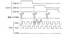
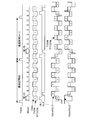
- FIG. 1 is a timing chart for explaining a driving method of the touch panel 20 according to the first embodiment.
- FIG. 1 shows the timing for synchronizing the operation of the liquid crystal panel 10 shown in FIG. 8 and the operation of the touch panel 20 shown in FIG.
- FIG. 1 shows a period in which Step B to Step E are repeated among the operations of the touch panel 20 described above. That is, in the driving method of the touch panel 20 according to the first embodiment, the control signal of the reset switch 44 is kept at L level during the display period on the liquid crystal panel 10, and the voltage is sequentially supplied to each X electrode 21. Switch on / off at least once.
- the control signal of the SSD switch 15 is at the beginning of the period when the control signal of the SSD switch 15 is at the H level (in other words, the SSD switch 15 is on).
- the timing control signal of the sampling switch 41 is kept at the L level in the touch panel 20. That is, in the touch panel 20, the terminal “0” of the sampling switch 41 is connected (ON state) in the initial period (fixed period) P, and the hold (step E) is maintained.
- the initial period P is preferably set according to the generation period obtained by analyzing the generation period of radiation noise from the liquid crystal panel 10 with an oscilloscope or the like. Specifically, the initial period P is preferably a period of 2 ⁇ s to 4 ⁇ s from the moment when the control signal of the SSD switch 15 is changed to the H level, that is, the moment when the voltage applied to the source bus line 13 is changed. However, if the resistance of the counter electrode of the liquid crystal panel 10 is reduced, the initial period P can be made shorter.
- the Y electrode 22 and the integrating circuit 42 are disconnected from each other during the generation of radiation noise. For this reason, even if the Y electrode 22 receives radiation noise generated from the display panel 10, the integration circuit 42 is not affected by the radiation noise from the Y electrode 22. Therefore, according to the driving method according to the first embodiment, the touch panel 20 is driven during the display period of the display panel 10 and the output voltage of the integration circuit 42 is not affected by radiation noise. Can be improved.
- the period during which the touch panel 10 is held is a period during which the touch panel 10 overlaps the initial period P as shown in FIG.
- the driving method according to the first embodiment is realized by the timing controller 48 (control means) also controlling the sampling switch 41, the signal generator 23, and the reset switch 44.
- FIG. 10 is a timing chart for explaining a driving method of the liquid crystal panel 10 according to the second embodiment. 10 shows the timing for synchronizing the operation of the liquid crystal panel 10 shown in FIG. 8 and the operation of the touch panel 20 shown in FIG.
- FIG. 10 shows a period in which Step B to Step E are repeated among the operations of the touch panel 20 described above. That is, also in the driving method of the touch panel 20 according to the second embodiment, similarly to the first embodiment, the control signal of the reset switch 44 is kept at the L level and the voltage is sequentially applied to the X electrodes 21 during the display period in the liquid crystal panel 10. The sampling switch 41 is turned on / off.
- the timing control signal of the sampling switch 41 is kept at the H level in the initial period P of the liquid crystal panel 10 and the touch panel 20. That is, in the touch panel 20, in the initial period P, the terminal “1” of the sampling switch 41 is connected (off state), and the charge transfer state (step E) is maintained. Therefore, in the second embodiment, the integration circuit 42 integrates the charge flowing from the Y electrode 22 before and after the generation of radiation noise.
- the period during which the touch panel 10 maintains the charge transfer state is preferably a period during which the touch panel 10 overlaps the initial period P, but may be a period that covers at least the initial period P.
- the counter electrode of the liquid crystal panel 10 serves as a noise source, and radiation noise generated from the counter electrode is added to the integration capacitance of the integration circuit 42 via the Y electrode 22 of the touch panel 20.
- the influence received by the touch panel 20 described here means the amount of noise Q noise added to the integration capacitance of the integration circuit 42. Therefore, in the following, a model expression of the noise amount in a simple model will be described.
- FIG. 11 is a diagram illustrating a relationship among the liquid crystal panel 10, the Y electrode 22 of the touch panel 20, and the integration circuit 42.
- a capacitor C sense-LCD is formed between the counter electrode or source bus line of the liquid crystal panel 10 and the Y electrode (sense line) 22 of the touch panel 20. This capacitance C sense-LCD is expressed by the following equation (1).
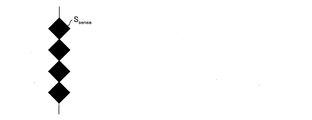
- Equation 1 S Sense represents the area per Y electrode 22 as shown in FIG. D represents the distance between the counter electrode of the liquid crystal panel 10 and the Y electrode 22 of the touch panel 20. Further, ⁇ represents a dielectric constant.
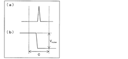
- FIGS. 12A and 12B are diagrams showing examples of radiation noise waveforms generated from the liquid crystal panel 10.
- FIG. 12A and 12B are diagrams showing examples of radiation noise waveforms generated from the liquid crystal panel 10.
- noise is generated, but no noise is generated both at the start of integration by the integration circuit 42 and at the end of integration, and therefore, between the start of integration and the end of integration.
- the noise voltage amplitude V noise is zero.
- FIG. 12B since noise is generated at the start of integration by the integration circuit 42 and no noise is generated at the end of integration, the noise voltage amplitude V between the start of integration and the end of integration. noise has a certain value.
- model expression of the noise amount Q noise received by the integration capacitor of the integration circuit 42 is expressed by the following expression (2).
- Qnoise Csense- LCD.Vnoise ... Formula (2)
- the terminal “1” of the sampling switch 41 is connected while the initial period P overlaps, and the Y electrode 22 is connected to the integrating circuit 42.
- noise is generated during integration by the integrating circuit 42, but no noise is generated at the start of integration, and the noise returns to the initial voltage at the end of integration. For this reason, the noise voltage amplitude V noise between the integration start time and the integration end time by the integration circuit 42 becomes zero.
- the amount of noise Q noise received by the integrating circuit 42 in the second embodiment is zero. That is, according to the driving method according to the second embodiment, the touch panel 20 is driven during the display period of the display panel 10, and the output voltage of the integration circuit 42 is not affected by radiation noise. Can be improved.
- FIG. 14 is an enlarged view showing a radiation noise waveform generated from the liquid crystal panel 10 and a timing control signal of the sampling switch 41 (switching element 41; SW41).
- the initial period P in which radiation noise occurs is shown in an enlarged manner.
- a common matter in the first and second embodiments is that the sampling switch 41 is not switched during the initial period P.
- the operation of switching the sampling switch 41 is performed.
- the timing control signal of the sampling switch 41 changes from L level to H level.
- the connection is switched from the terminal “0” to the terminal “1”, and the integration by the integration circuit 42 starts in the middle of the initial period P.
- the noise voltage amplitude V noise between the start of integration and the end of integration has an arbitrary value. Therefore, the noise amount Q noise received by the integration circuit 42 in the first comparative example has a value obtained from the above equation (2).
- the touch panel 20 performs the detection operation without switching the sampling switch 41 in the initial period P, so that the integration capacitance of the integration circuit 42 receives noise while driving the touch panel 20 in the display period of the display panel 10. Can be avoided. According to such a detection operation, the detection accuracy of the touch panel 20 can be improved.
- the touch panel drive frequency (frequency of voltage output by the integration circuit 42) is limited to 60 Hz as in the conventional technique (for example, Non-Patent Document 1). Absent. For example, when handwritten input such as a pen is performed, the pen tip moves at a high speed, so that generally a touch panel drive frequency of 180 Hz to 240 Hz or more is required. Therefore, this embodiment has an advantage over high-speed input using a pen or the like.
- the sensing time is limited to about 2 ms.
- the detection operation (steps A to F described above) by the touch panel 20 can be performed without time-dividing the frame.
- the sensing time charge transfer time
- FIG. 15 is a cross-sectional view illustrating a schematic configuration of a liquid crystal display device 1a having a configuration in which a touch panel is in-celled in a liquid crystal panel.
- the liquid crystal display device 1 a is configured by laminating a cover glass 30 on a liquid crystal panel 20 a in which the touch panel 20 is in-celled.
- the touch panel 20 is provided in-cell inside the liquid crystal panel 20a. Therefore, it is not necessary to separately arrange the touch panel 20 on the surface of the liquid crystal panel 20a, and the liquid crystal display device 1a can be further downsized.
- FIG. 16A is a diagram illustrating a planar structure of the liquid crystal panel 10.
- FIG. 16B is a diagram illustrating an equivalent circuit of one pixel included in the liquid crystal panel 10.
- FIG. 16C is a diagram showing a cross section of the liquid crystal panel 10.
- the liquid crystal panel 10 includes a counter-side glass substrate 51, a TFT-side glass substrate 52, and a liquid crystal layer 53 sandwiched therebetween.
- a common electrode (upper electrode) 54 is formed on the surface of the opposite glass substrate 51 facing the liquid crystal layer 53.
- a pixel electrode (lower electrode) 55 is formed on the surface of the TFT side glass substrate 52 facing the liquid crystal layer 53. Therefore, the liquid crystal layer 53 is sandwiched between the common electrode 54 and the pixel electrode 55.
- the liquid crystal panel 10 is provided with a matrix pixel array composed of a plurality of scanning signal lines (GL) and a plurality of data signal lines (SL).
- FIG. 16B shows an equivalent circuit of one pixel.
- TCOM corresponds to the common electrode 55
- Vpixel corresponds to the pixel electrode 55.
- the TCOM is formed on the opposing glass substrate 51 so as to cover the entire surface of the pixel array.
- Vpixel is formed separately for each pixel.
- the liquid crystal panel 10 applies an arbitrary voltage to the liquid crystal layer 62 (LC) by controlling the electrode applied to Vpixel.
- the liquid crystal display device 1 controls the alignment state of the liquid crystal layer 53 by applying a predetermined voltage between the common electrode 54 and the pixel electrode 55. Thereby, the transmittance of light passing through the liquid crystal layer 53 is controlled.
- the common electrode 54 TCOM
- AC alternating current
- DC direct current
- FIG. 17 is a diagram illustrating various voltage waveforms when the common electrode 54 of the liquid crystal panel 10 is AC driven.
- one period of the vertical synchronizing signal Vsync corresponds to a period of one frame, and is usually 1/60 second, that is, about 16.6 ms.
- the gate driver 11 sequentially scans the scanning signal GL one by one during one frame.
- a counter electrode driver (voltage applying means) (not shown) applies an AC voltage to the counter electrode 54 (TCOM).
- the source driver 12 applies a voltage having an arbitrary amplitude to the pixel electrode 55 (Vpixel). By applying these voltages, the voltage applied to the liquid crystal layer 53 is controlled.
- the amplitude of the voltage applied to the Vpixel can be suppressed to about half compared with the DC driving of the TCOM described later, so that the power consumption can be further reduced.
- FIG. 18 is a diagram showing various voltage waveforms when the common electrode 54 of the liquid crystal panel 10 is DC-driven.
- the counter electrode driver applies a DC voltage to the counter electrode 54 (TCOM).
- the source driver 12 applies a voltage having an arbitrary amplitude to the pixel electrode 55 (Vpixel). By applying these voltages, the voltage applied to the liquid crystal layer 53 is controlled. It can be said that the DC drive of TCOM is a simpler system than the AC drive of TCOM described above. However, the amplitude of the voltage applied to Vpixel tends to be relatively large.
- the liquid crystal panel 10 according to the present embodiment reduces the number of lines connected to the source driver 12 by adopting the SSD method, but one embodiment of the present invention is not limited to this, and the SSD is not limited thereto. It is not necessary to adopt the method.
- an initial period from the moment when the voltage of the source bus line 13 is changed to the next time when the voltage is changed may be an initial period P.
- touch panel 20 is a mutual capacitance method
- one embodiment of the present invention can also be applied to a self-capacitance method.
- the certain period is set in advance in accordance with a generation period of radiation noise from the display panel.
- the certain period is preferably 2 ⁇ s to 4 ⁇ s.
- the influence of radiation noise generated from the display panel can be suppressed more appropriately. Therefore, the detection accuracy of a touch panel can be improved more suitably.
- the display panel further includes means for generating a synchronization signal, and the touch panel operates in accordance with the synchronization signal.
- the touch panel is preferably a mutual capacitive touch panel.
- a display device including a mutual capacitive touch panel with high detection accuracy can be realized.
- the display panel further includes an SSD switch.
- an SSD display device including a touch panel with high detection accuracy can be realized.
- the display device with a touch panel preferably further includes voltage application means for applying a DC voltage to the counter electrode of the display panel.
- the present invention can be suitably used for a display device with a touch panel.
Landscapes
- Engineering & Computer Science (AREA)
- General Engineering & Computer Science (AREA)
- Theoretical Computer Science (AREA)
- Human Computer Interaction (AREA)
- Physics & Mathematics (AREA)
- General Physics & Mathematics (AREA)
- Position Input By Displaying (AREA)
- Control Of Indicators Other Than Cathode Ray Tubes (AREA)
Abstract
タッチパネル(20)は、互いに直交する複数のドライブライン(21)及び複数のセンスラインと、センスラインに接続されたサンプリングスイッチ(41)と、サンプリングスイッチ(41)を介してセンスラインに接続される積分回路とを備えている。サンプリングスイッチ(41)は、ソースバスラインの電圧が変化する瞬間から一定期間(P)、オン状態またはオフ状態を保つ。
Description
本発明は、静電容量型タッチパネルを有する表示装置及びその駆動方法に関するものである。
近年、Apple社製のi-Phone(登録商標)やi-Pad(登録商標)等により代表される、静電容量型タッチパネル付き表示装置の利用が広まっている。静電容量型タッチパネルは、指の非接触時と接触時におけるそれぞれの電極の容量差によって検出出力を得ている。
従来の静電容量型タッチパネル付き表示装置の典型例について、図19を参照して説明する。図19は、従来の静電容量型タッチパネル付き液晶表示装置の概略的な構成を示す断面図である。この図に示すように、従来の液晶表示装置100は、液晶パネル(LCD:Liquid Crystal Display)100、タッチパネル(TP:Touch Panel)200、カバーガラス300が順に積層されることにより構成されている。タッチパネル200はエアギャップを介して液晶パネル100上に配置されている。
また、近年、タッチパネルのコスト低減、モジュール薄型化、軽量化、高機能化が求められており、これらを達成するためにタッチパネルと表示装置との一体化(インセル化)が進められている。例えば、将来的には、液晶表示装置と一体化されたタッチパネルは、液晶パネルとの間にエアギャップがない構成で配置されることによって、タッチパネルのタッチ機能層と液晶パネルとの間の距離がより近くなっていく。
静電容量型タッチパネルは、上述のように一体化(インセル化)された場合、液晶パネルが発生するノイズの影響を強く受けることになる。すなわち、液晶パネルが表示を行いながらタッチパネルが検出動作を行う際、液晶パネルから発生する輻射ノイズがタッチパネルの検出感度に悪影響を及ぼしてしまう。そこで、静電容量型タッチパネルの性能が低下することを防ぐためには、液晶パネルからのノイズの影響を低減させる技術が開発されている。
例えば、非特許文献1に開示された技術では、フレームを時分割し、液晶パネルが表示駆動を行っていない期間(フレーム間の表示を行っていない期間)にタッチパネルを駆動させることによって、タッチパネルが液晶パネルから受けるノイズを低減させている。
「Touch Panel Embedded IPS-LCD with parasitic Current Reduction Technique」, Hiroshi Haga et. al.,SID 2010,p.669-672
しかしながら、非特許文献1に開示された技術では、1フレームの表示期間(約14ms)を確保する必要があるために、タッチパネルのセンシング時間に上限が存在する。このため、タッチパネルが検出するシグナルは低下し、タッチパネルの性能を効果的に向上させることができない。
また、非特許文献1に開示された技術では、フレーム間の表示を行っていない期間を利用してタッチパネルを駆動するため、タッチパネルにおける座標出力の周波数は60Hzに限定されてしまう。例えば、ペンなどの手書き入力による高速入力を検出するためには、一般的に、座標出力の周波数が180Hz~240Hz以上必要である。非特許文献1に開示された技術では、このようなタッチパネルの高速駆動に対して対応することができない。
本発明は、上記の問題に鑑みてなされたものであり、その目的は、タッチパネルにおける座標出力の周波数を制限されずに、ノイズの影響を抑えて検出精度を向上させたタッチパネル付き表示装置を提供することにある。
本発明者らは、上記課題を解決するために鋭意検討したところ、表示装置における表示パネルでは、データ信号線に供給される電圧が変化した瞬間に輻射ノイズが発生することを見出した。
そこで、本発明の一態様に係るタッチパネル付き表示装置は、上記課題を解決するために、表示パネルと、前記表示パネルの観測者側の面上に配置されるかまたは前記表示パネルの内部に設けられる静電容量型のタッチパネルとを備えるタッチパネル付き表示装置であって、
前記表示パネルは、
互いに直交する複数のデータ信号線及び複数の走査信号線と、
前記複数のデータ信号線の各々に対して順に電圧を供給するデータ信号線駆動回路とを備えており、
前記タッチパネルは、
互いに直交する複数の送信電極及び複数の受信電極と、
積分回路と、
前記複数の受信電極のいずれか1つと前記積分回路とを接続するスイッチング素子と、
前記複数のデータ信号線に電圧が供給されている間に、少なくとも1回以上、前記スイッチング素子のオン・オフを切り替える制御手段とを備えており、
前記制御手段は、前記データ信号線駆動回路が前記電圧を変化させた瞬間から一定期間、前記スイッチング素子のオン状態またはオフ状態を保つことを特徴としている。
前記表示パネルは、
互いに直交する複数のデータ信号線及び複数の走査信号線と、
前記複数のデータ信号線の各々に対して順に電圧を供給するデータ信号線駆動回路とを備えており、
前記タッチパネルは、
互いに直交する複数の送信電極及び複数の受信電極と、
積分回路と、
前記複数の受信電極のいずれか1つと前記積分回路とを接続するスイッチング素子と、
前記複数のデータ信号線に電圧が供給されている間に、少なくとも1回以上、前記スイッチング素子のオン・オフを切り替える制御手段とを備えており、
前記制御手段は、前記データ信号線駆動回路が前記電圧を変化させた瞬間から一定期間、前記スイッチング素子のオン状態またはオフ状態を保つことを特徴としている。
上記構成では、タッチパネルにおいて、送信電極に供給された電圧が変化する際、受信電極から電荷が流れる。このときスイッチング素子はオン状態になっており、受信電極と積分回路とを接続している。積分回路が受信電極から流れる電荷を積分することによって、タッチパネルはタッチ検出を行うことができる。
また、上記構成では、データ信号線駆動回路がデータ信号線に対して表示のための電圧を供給している間、スイッチング素子は、少なくとも1回以上、オン・オフを切り替えられる。すなわち、タッチパネルは、表示パネルによる表示期間に、タッチ検出のための駆動を行うことになる。
さらに、上記構成において、スイッチング素子は、データ信号線の電圧が変化した瞬間から一定期間、オン状態またはオフ状態を保っている。
例えば、上記一定期間にスイッチング素子がオフ状態を保っている場合、ノイズが発生している間、受信電極と積分回路とは切り離されていることになる。よって、積分回路は輻射ノイズの影響を受けることを回避することができる。
また、上記初期期間の間にスイッチング素子がオン状態を保っている場合、積分回路はノイズの発生前から発生後までの間、受信電極から流れる電荷を積分することになる。このため、積分開始時と積分終了時との間におけるノイズ源の電位振幅Vnoiseは0になる。ここで、積分回路に影響を与えるノイズ量Qnoiseは、モデル式によれば、液晶パネルと受信電極との間に形成される容量Csense‐LCDと、積分開始時と積分終了時との間におけるノイズ源の電位振幅Vnoiseとの積により求められる。このため、ノイズ源の電位振幅Vnoiseは0であれば、ノイズ量Qnoiseは0になる。よって、積分回路はノイズの影響を受けることなしに、受信電極から流れる電荷を積分することができる。
以上のように、本発明の一態様に係るタッチパネル付き表示装置は、ノイズの影響を抑制しつつ、表示パネルの表示期間にもタッチパネルの駆動を行うことによって、タッチパネルの検出時間を十分に確保することができる。これによって、タッチパネルの検出精度を向上させることができる。また、積分回路による出力(座標出力)の周波数が60Hzに制限されないため、タッチパネルに対する高速入力に対して、好適に対応することができる。
本発明の一態様に係るタッチパネル付き表示装置の動作方法は、表示パネルと、前記表示パネルの観測者側の面上に配置されるかまたは前記表示パネルの内部に設けられる静電容量型のタッチパネルとを備えるタッチパネル付き表示装置の動作方法であって、
前記表示パネルは、
互いに直交する複数のデータ信号線及び複数の走査信号線と、
前記複数のデータ信号線の各々に対して順に電圧を供給するデータ信号線駆動回路とを備えており、
前記タッチパネルは、
互いに直交する複数の送信電極及び複数の受信電極と、
積分回路と、
前記複数の受信電極のいずれか1つと前記積分回路とを接続するスイッチング素子と、
前記複数のデータ信号線に電圧が供給されている間に、少なくとも1回以上、前記スイッチング素子のオン・オフを切り替える制御手段とを備えており、
前記制御手段は、前記データ信号線駆動回路が前記電圧を変化させた瞬間から一定期間、前記スイッチング素子のオン状態またはオフ状態を保つことを特徴とする。
前記表示パネルは、
互いに直交する複数のデータ信号線及び複数の走査信号線と、
前記複数のデータ信号線の各々に対して順に電圧を供給するデータ信号線駆動回路とを備えており、
前記タッチパネルは、
互いに直交する複数の送信電極及び複数の受信電極と、
積分回路と、
前記複数の受信電極のいずれか1つと前記積分回路とを接続するスイッチング素子と、
前記複数のデータ信号線に電圧が供給されている間に、少なくとも1回以上、前記スイッチング素子のオン・オフを切り替える制御手段とを備えており、
前記制御手段は、前記データ信号線駆動回路が前記電圧を変化させた瞬間から一定期間、前記スイッチング素子のオン状態またはオフ状態を保つことを特徴とする。
上記方法によれば、本発明の一態様に係るタッチパネル付き表示装置に関して上述した効果と同様の効果を奏する。
本発明の他の目的、特徴、および優れた点は、以下に示す記載によって十分分かるであろう。また、本発明の利点は、添付図面を参照した次の説明で明白になるであろう。
本発明の一態様に係るタッチパネル付き表示装置は、表示パネルと、前記表示パネルの観測者側の面上に配置される静電容量型のタッチパネルとを備えるタッチパネル付き表示装置であって、前記表示パネルは、互いに直交する複数のデータ信号線及び複数の走査信号線と、前記複数のデータ信号線の各々に対して順に電圧を供給するデータ信号線駆動回路とを備えており、前記タッチパネルは、互いに直交する複数の送信電極及び複数の受信電極と、積分回路と、前記複数の受信電極のいずれか1つと前記積分回路とを接続するスイッチング素子と、前記複数のデータ信号線に電圧が供給されている間に、少なくとも1回以上、前記スイッチング素子のオン・オフを切り替える制御手段とを備えており、前記制御手段は、前記データ信号線駆動回路が前記電圧を変化させた瞬間から一定期間、前記スイッチング素子のオン状態またはオフ状態を保つため、タッチパネルの検出精度を好適に向上させることができる。
以下、図面を参照して、本発明の一実施形態に係る液晶表示装置の一実施形態について説明する。
〔1.液晶表示装置1について〕
図2は、本実施形態に係る液晶表示装置(タッチパネル付き表示装置)1の概略的な構成を示す断面図である。
図2は、本実施形態に係る液晶表示装置(タッチパネル付き表示装置)1の概略的な構成を示す断面図である。
図2に示すように、液晶表示装置1は、液晶パネル(LCD:Liquid Crystal Display)10、タッチパネル(TP:Touch Panel)20、カバーガラス30が順に積層されることにより構成されている。タッチパネル20は、液晶パネル10における観察者側の面上に直接配置されている。すなわち、液晶パネル10とタッチパネル20との間にはエアギャップがない。
本実施形態において、タッチパネル20は静電容量型タッチパネルである。カバーガラス30上に観察者の指2が接触すると、指2とタッチパネル20の電極との間には容量が形成される。タッチパネル20は、指2の非接触時と接触時におけるそれぞれの電極の容量差によって、指のタッチまたは非タッチを検出している。
〔2.タッチパネル20について〕
(タッチパネル20の構成)
図3は、タッチパネル20が備えるX電極(送信電極;送信ライン;ドライブライン)21と及びY電極(受信電極;受信ライン;センスライン)22を示す上面図である。図3に示すように、タッチパネル20の基板上には、複数のX電極21が配置され、これらと直交するように複数のY電極が配置されている。X電極21及びY電極22は、それぞれ、その延伸方向に沿って幅広部と幅狭部とが交互に配列されたパターンをなして形成されている。
(タッチパネル20の構成)
図3は、タッチパネル20が備えるX電極(送信電極;送信ライン;ドライブライン)21と及びY電極(受信電極;受信ライン;センスライン)22を示す上面図である。図3に示すように、タッチパネル20の基板上には、複数のX電極21が配置され、これらと直交するように複数のY電極が配置されている。X電極21及びY電極22は、それぞれ、その延伸方向に沿って幅広部と幅狭部とが交互に配列されたパターンをなして形成されている。
図4は、タッチパネル20の備える処理回路40を示す図である。
図4に示すように、処理回路40は、X電極21に接続された信号発生器23、Y電極22に接続されたサンプリングスイッチ41、積分回路42、アンプ43、リセットスイッチ(リセット手段)44、電荷キャンセル回路45、検出器47、及びタイミングコントローラ48を備えている。また、本実施形態において、タッチパネル20は相互容量方式を採用しており、X電極21とY電極22とは容量24によって結合している。
図4に示す処理回路40は、図3に示す複数のX電極21及び複数のY電極22のうち、任意のX電極21及びY電極22に対する処理回路を代表して示している。すなわち、本実施形態では、複数のY電極22の各々に対応して、サンプリングスイッチ41、積分回路42、アンプ43、及びリセットスイッチ44等がそれぞれ設けられているものとする。複数のY電極22の各々は、各サンプリングスイッチ41を介して、各積分回路42にそれぞれ接続する。また、検出器47は、処理回路40に配置された全ての積分回路42と接続可能なように1つ配置されている。すなわち、検出器47は、処理回路40ごとに、換言すればY電極22ごとに配置されている。しかし、本発明の一実施形態はこれに限らず、複数のY電極22に対して共通の1つの検出器47を配置する構成であってもよい。
信号発生器23は、周期的な電圧信号をX電極に出力する。X電極に供給される電圧信号がHレベルからLレベル、またはLレベルからHレベルに変化したときに、Y電極22に電流が流れる。
サンプリングスイッチ41は、Y電極22と積分回路42との間に配置される。サンプリングスイッチ41は、信号発生器23が電圧信号をLレベルからHレベルに変化させるとき、端子「1」に接続されていることによりオン状態になっている。これにより、Y電極22と積分回路42とを接続している。一方、信号発生器23が電圧信号をHレベルからLレベルに変化させるとき、端子「0」に接続されていることによりオフ状態になっている。これにより、Y電極22を接地させている。
リセットスイッチ44は、オン状態のときに積分回路42を接地させ、その積分容量をリセットする。リセットスイッチ44は、オン・オフの切り替えにより、タッチパネル20における検出期間を所定の周期に制御する。
信号発生器23による電圧信号の出力タイミングと、サンプリングスイッチ41及びリセットスイッチ44のオン・オフのタイミングとは、タイミングコントローラ48によって制御される。
積分回路42は、オペアンプ及び積分容量Csから構成される。積分容量Csは、サンプリングスイッチ41がオンの時、Y電極22に流れた電荷を蓄積する。ここで、指の非接触時と接触時とでは容量24が変化する(指の接触時には容量が小さくなる)。このため、積分回路42は、Y電極22に流れた電流値を積分することにより、X電極21とY電極22との結合容量24の容量差に比例する電圧を出力する。
検出器47は、積分回路42による出力電圧の差を計測することによって、指の接触または非接触を検出する。
なお、処理回路40の構成は、上述のものに限られず、タッチパネル20は、複数のY電極22に対して選択的に接続するように設けられた積分回路42、アンプ43、及びリセットスイッチ44をそれぞれ備えていてもよい。処理回路40の詳細な構成については、米国特許6,452,514号を参照することができる。
(タッチパネル20の動作)
次に、タッチパネル20の動作について図5及び図6を参照して説明する。
次に、タッチパネル20の動作について図5及び図6を参照して説明する。
図5は、タッチパネル20の動作を説明するためのタイミングチャートの一例を示す図である。また、図6は、タッチパネル20の動作の工程をまとめた表を示す図である。
なお、図5では、任意のある1つのX電極21に供給される電圧の波形を示している。また、図5において、各サンプリングスイッチ41及び各リセットスイッチ44の各々に入力されるタイミング制御信号、任意の積分回路42の出力電圧の例を示している。
また、図6において、サンプリングスイッチ41における端子「0」および端子「1」、ならびにリセットスイッチ44について、記号「×」は接続状態を示し、記号「-」は非接続状態を示す。
図5及び図6に示すように、タッチパネル20は、以下のステップA~Fを繰り返して行う。
まず、リセットスイッチ44がタイミング制御信号によりオフ状態になる。これによって、積分回路42の積分容量が初期状態(例えば0V)にリセットされる(ステップA)。
次いで、リセットスイッチ44がオン状態になった後、X電極21に供給される電圧信号がLレベルからHレベルに変化する間、サンプリングスイッチ41は、タイミング制御信号により端子「1」を接続する。これにより、Y電極22は、端子「1」を介して積分回路42に接続される。このとき、Y電極22から流れる電荷が積分回路42の積分容量に転送される(ステップC)。
その後、サンプリングスイッチ41はタイミング制御信号により端子「0」を接続し、Y電極22は端子「0」を介して電気的に接地される。これにより、積分回路42内の電荷は保持され、ホールド状態になる(ステップE)。
なお、ステップB及びステップDはデッドタイムであり、いずれのスイッチ及び端子も接続されない状態である。
本実施形態では、1つのあるX電極21において、ステップBからステップEまでを少なくとも1回繰り返することによって、少なくとも1回積分を行う。そして、当該あるX電極21の処理が終われば、リセット処理を実行し、それから、次のX電極21において、ステップBからステップEまでを少なくとも1回繰り返し実行する。
最後の電荷転送(ステップC)を行った後、サンプリングスイッチ41が端子「0」を接続してホールド状態を維持する間、検出器47が積分回路42の出力電圧を測定する(ステップF)。測定後、リセットスイッチ44はタイミング制御信号により再びオフ状態になり、ステップAに戻ることができる。
〔3.液晶パネル10について〕
(液晶パネル10の構成)
次に、液晶パネル10の構成について図7を参照して簡単に説明する。
(液晶パネル10の構成)
次に、液晶パネル10の構成について図7を参照して簡単に説明する。
図7は、液晶パネル10におけるアクティブマトリクス基板上の電極構成を示す図である。
液晶パネル10は、アクティブマトリクス基板と対向基板との間に液晶層を挟むことにより構成される。アクティブマトリクス基板には、複数のソースバスライン(データ信号線)13と、複数のゲートバスライン(走査信号線)14とが配置されている。アクティブマトリクス基板において、複数のソースバスライン13と複数のゲートバスライン14とは互いに直行し、表示領域をマトリクス状に分割している。
また、本実施の形態に係る液晶パネル10は、SSD(Source Shared Driving)方式のアクティブマトリクス型液晶パネルである。複数のソースバスライン13は、表示色を構成する3原色、すなわち赤(R)、緑(G)、青(B)の各副画素に対応して配置されており、R、G、Bに対応する3本を一組として構成されている。ソースバスライン13とゲートバスライン14との交点には、各色に対応する副画素がそれぞれ形成され、これにより画素が構成される。
複数のソースバスライン13は、組ごとに、SSDスイッチ15を介してソースドライバ(データ信号線駆動回路)12に接続される。SSDスイッチ15は、制御回路(図示しない)による制御信号によってオン/オフを制御され、複数のソースバスライン13は、順次、ソースドライバ12に接続される。すなわち、複数のソースバスライン13は、各組ごとに、RGBの順にデータ信号(電圧信号)を供給される。
また、複数のゲートバスライン14はゲートドライバ(走査信号線駆動回路)11に接続されている。複数のゲートバスライン14は、ゲートドライバ11によって順次選択され、走査信号が供給される。
表示パネル10は、ゲートバスライン14が選択されている間、選択されたゲートバスライン14に接続されている画素に対して、ソースバスライン13からデータ信号を供給することによって書き込みを行う。これによって表示パネル10の表示が行われる。
なお、図7に示すソースバスライン13及びゲートバスライン14の数は例示的なものであり、特に限定されない。
(液晶パネル10の動作)
次に、液晶パネル10の動作について、図8を用いて説明する。図8は、液晶パネル10の動作を説明するためのタイミングチャートの一例を示す図である。
次に、液晶パネル10の動作について、図8を用いて説明する。図8は、液晶パネル10の動作を説明するためのタイミングチャートの一例を示す図である。
図8において、SSD(R),SSD(G),SSD(B)は、SSDスイッチ15を、R,G,Bに対応する各ソースバスライン13に接続するための制御信号を示している。GL(n)は、例示的なn番目のゲートバスライン14の電位を示し、SL(R),SL(G),SL(B)は、R、G、Bの各副画素に対応する各ソースバスライン13の電位を示している。
図8に示すように、本実施形態に係る液晶パネル10の駆動方法は、1水平走査期間にデータ信号を3分割して出力するものである。各SSDスイッチ15は、制御信号がHレベルのときにオン状態になる。具体的には、SSDスイッチ15は、R、G、Bに対応する各制御信号がHレベルのときに、当該色に対応するソースバスライン13と接続する。これにより、ソースドライバ12と接続されたソースバスライン13には所望のソース電圧が印加される。このとき、選択されたゲートバスライン14上において、当該ソースバスライン13と接続された表示画素には書き込みが行われる。
(液晶パネル10から発生する輻射ノイズ)
ここで、本発明者らは、液晶パネル10から発生する輻射ノイズを解析した結果、図9に示すような波形を得ることができた。図9は、液晶パネル10の駆動波形とノイズ波形とを示す図である。図9に示すように、液晶パネル10では、SSDスイッチ15がオンになった瞬間にノイズが発生している。すなわち、本発明者らは、ソースバスライン13に加わる電圧が変化した瞬間にノイズが発生することを見出した。
ここで、本発明者らは、液晶パネル10から発生する輻射ノイズを解析した結果、図9に示すような波形を得ることができた。図9は、液晶パネル10の駆動波形とノイズ波形とを示す図である。図9に示すように、液晶パネル10では、SSDスイッチ15がオンになった瞬間にノイズが発生している。すなわち、本発明者らは、ソースバスライン13に加わる電圧が変化した瞬間にノイズが発生することを見出した。
〔4.液晶パネル10とタッチパネル20の同期〕
本実施形態では、液晶パネル10に駆動に対してタッチパネル20の駆動を同期させることによって、タッチパネル20は、液晶パネル10から発生する輻射ノイズの影響を受けないようにすることができる。このような効果を発揮するための、液晶パネル10と同期させたタッチパネル20との駆動方法について、以下に説明する。
本実施形態では、液晶パネル10に駆動に対してタッチパネル20の駆動を同期させることによって、タッチパネル20は、液晶パネル10から発生する輻射ノイズの影響を受けないようにすることができる。このような効果を発揮するための、液晶パネル10と同期させたタッチパネル20との駆動方法について、以下に説明する。
(実施例1)
図1は、実施例1に係るタッチパネル20の駆動方法を説明するためのタイミングチャートである。なお、図1は、図8に示す液晶パネル10における動作と、図5に示すタッチパネル20における動作とを同期させるタイミングを示すものである。
図1は、実施例1に係るタッチパネル20の駆動方法を説明するためのタイミングチャートである。なお、図1は、図8に示す液晶パネル10における動作と、図5に示すタッチパネル20における動作とを同期させるタイミングを示すものである。
図1は、上述したタッチパネル20の動作うち、ステップBからステップEが繰り返される期間を示している。すなわち、実施例1に係るタッチパネル20の駆動方法では、液晶パネル10における表示期間において、リセットスイッチ44の制御信号をLレベルに保ち、各X電極21に電圧を順次供給し、各サンプリングスイッチ41のオン・オフを少なくとも1回以上切り替えている。
また図1に示すように、実施例1に係るタッチパネル20の駆動方法では、SSDスイッチ15の制御信号がHレベル(SSDスイッチ15がオン状態)の期間の初期、言い換えると、ソースバスライン13に表示のための電圧が供給される期間の初期(以下、初期期間Pと称する)において、タッチパネル20においてサンプリングスイッチ41のタイミング制御信号をLレベルに保っている。すなわち、タッチパネル20では、初期期間(一定期間)Pにおいて、サンプリングスイッチ41の端子「0」が接続し(オン状態)、ホールド(ステップE)が保たれる。
なお、初期期間Pは、液晶パネル10からの輻射ノイズの発生期間をオシロスコープなどにより分析し、求められた発生期間に合わせて設定することが好ましい。具体的には、初期期間Pは、SSDスイッチ15の制御信号をHレベルに変化させた瞬間、すなわちソースバスライン13に加わる電圧が変化した瞬間から2μs~4μsの期間であることが好ましい。ただし、液晶パネル10の対向電極の抵抗を低減させれば、初期期間Pをさらに短い期間にすることも可能である。
したがって、実施例1に係る駆動方法では、輻射ノイズの発生中、Y電極22と積分回路42とが非接続状態になる。このため、例えY電極22が表示パネル10から発生する輻射ノイズを受けたとしても、積分回路42は、Y電極22から当該輻射ノイズの影響を受けることはない。よって、実施例1に係る駆動方法によれば、表示パネル10の表示期間にタッチパネル20を駆動させつつ、積分回路42の出力電圧に輻射ノイズの影響が乗ることはないため、タッチパネル20の検出精度を向上させることができる。
なお、タッチパネル10がホールドを保つ期間は、図1に示すように、初期期間Pにオーバーラップする間であることが好ましいが、少なくとも初期期間Pをカバーする期間であればよい。
また、実施例1に係る駆動方法は、タイミングコントローラ48(制御手段)が、サンプリングスイッチ41、信号発生器23、及びリセットスイッチ44も制御することによって実現される。
(実施例2)
図10は、実施例2に係る液晶パネル10の駆動方法を説明するためのタイミングチャートである。なお、図10は、図8に示す液晶パネル10における動作と、図5に示すタッチパネル20における動作とを、同期させるタイミングを示すものである。
図10は、実施例2に係る液晶パネル10の駆動方法を説明するためのタイミングチャートである。なお、図10は、図8に示す液晶パネル10における動作と、図5に示すタッチパネル20における動作とを、同期させるタイミングを示すものである。
図10は、上述したタッチパネル20の動作うち、ステップBからステップEが繰り返される期間を示している。すなわち、実施例2に係るタッチパネル20の駆動方法においても、実施例1と同様に、液晶パネル10における表示期間において、リセットスイッチ44の制御信号をLレベルに保ち、各X電極21に電圧を順次供給し、各サンプリングスイッチ41のオン・オフを切り替えている。
図10に示すように、実施例2に係る液晶パネル10の駆動方法では、液晶パネル10における初期期間P、タッチパネル20において、サンプリングスイッチ41のタイミング制御信号がHレベルを保っている。すなわち、タッチパネル20では、初期期間Pにおいて、サンプリングスイッチ41の端子「1」が接続し(オフ状態)、電荷転送の状態(ステップE)が保たれる。よって、実施例2では、輻射ノイズの発生前から発生後までの間、積分回路42がY電極22から流れる電荷を積分していることになる。
なお、その他の事項については、実施例1における説明と同様である。例えば、タッチパネル10が電荷転送の状態を保つ期間は、初期期間Pにオーバーラップする間であることが好ましいが、少なくとも初期期間Pをカバーする期間であればよい。
ここで、実施例2の効果を説明する前に、液晶パネル10から発生する輻射ノイズによって、タッチパネル20が受ける影響について説明する。
本実施形態では、液晶パネル10の対向電極がノイズ源となり、この対向電極から発生した輻射ノイズが、タッチパネル20のY電極22を介して積分回路42の積分容量に加えられる。すなわち、ここで説明するタッチパネル20が受ける影響とは、積分回路42の積分容量に加えられるノイズ量Qnoiseを意味する。よって、以下では、シンプルなモデルにおけるノイズ量のモデル式について説明する。
図11は、液晶パネル10、タッチパネル20のY電極22、及び積分回路42の関係を示す図である。図11に示すように、液晶パネル10の対向電極またはソースバスラインと、タッチパネル20のY電極(センスライン)22との間には、容量Csense‐LCDが形成される。この容量Csense‐LCDは以下の式(1)により表される。

なお、式1において、SSenceは、図13に示すように1本のY電極22あたりの面積を表す。また、dは、液晶パネル10の対向電極と、タッチパネル20のY電極22との間の距離を表す。また、εは誘電率を表す。
図12の(a)および(b)は、液晶パネル10から発生する輻射ノイズ波形の例を示す図である。なお説明のために、タッチパネル20が上述のステップCを行う間、すなわち、積分回路42が積分を行っている間に、図12の(a)および(b)に示すような輻射ノイズが発生したものと仮定する。
図12の(a)では、ノイズが発生しているが、積分回路42による積分開始時と積分終了時との両方ではノイズが発生していないため、積分開始時と積分終了時との間のノイズ電圧振幅Vnoiseが0である。一方、図12の(b)では、積分回路42による積分開始時にノイズが発生しており、積分終了時にはノイズが発生していないため、積分開始時と積分終了時との間のノイズ電圧振幅Vnoiseはある値を有する。
以上をまとめると、積分回路42の積分容量が受けるノイズ量Qnoiseのモデル式は、以下の式(2)により表される。
Qnoise=Csense‐LCD・Vnoise ・・・式(2)
実施例2では、初期期間Pにオーバーラップする間、サンプリングスイッチ41の端子「1」が接続されており、Y電極22は積分回路42と接続している。ここで、積分回路42による積分の途中にノイズが発生しているが、積分開始時にはノイズが発生しておらず、また、積分終了時にはノイズが初期電圧に戻っている。このため、積分回路42による積分開始時と積分終了時との間のノイズ電圧振幅Vnoiseは0になる。
実施例2では、初期期間Pにオーバーラップする間、サンプリングスイッチ41の端子「1」が接続されており、Y電極22は積分回路42と接続している。ここで、積分回路42による積分の途中にノイズが発生しているが、積分開始時にはノイズが発生しておらず、また、積分終了時にはノイズが初期電圧に戻っている。このため、積分回路42による積分開始時と積分終了時との間のノイズ電圧振幅Vnoiseは0になる。
したがって、上記式(2)によれば、実施例2において積分回路42が受けるノイズ量Qnoiseは0になる。すなわち、実施例2に係る駆動方法によれば、表示パネル10の表示期間にタッチパネル20を駆動させつつ、積分回路42の出力電圧に輻射ノイズの影響が乗ることはないため、タッチパネル20の検出精度を向上させることができる。
(比較例との比較)
次に、実施例1及び2による作用効果について、図14を参照し、比較例1及び2と比較しながら説明する。図14は、液晶パネル10から発生する輻射ノイズ波形と、サンプリングスイッチ41(スイッチング素子41;SW41)のタイミング制御信号とを拡大して示す図である。なお、図14では、輻射ノイズが発生する初期期間Pを拡大して示している。
次に、実施例1及び2による作用効果について、図14を参照し、比較例1及び2と比較しながら説明する。図14は、液晶パネル10から発生する輻射ノイズ波形と、サンプリングスイッチ41(スイッチング素子41;SW41)のタイミング制御信号とを拡大して示す図である。なお、図14では、輻射ノイズが発生する初期期間Pを拡大して示している。
図14に示すように、実施例1及び2において共通する事項は、初期期間Pの間に、サンプリングスイッチ41を切り替えないということである。一方、比較例1及び2では、初期期間Pの間に、サンプリングスイッチ41を切り替える動作を行っている。
具体的には、比較例1では、初期期間Pの間に、サンプリングスイッチ41のタイミング制御信号がLレベルからHレベルに変化している。これによって、サンプリングスイッチ41では、端子「0」から端子「1」に接続が切り替えられ、初期期間Pの途中から積分回路42による積分が開始する。このため、積分開始時と積分終了時との間におけるノイズ電圧振幅Vnoiseは任意の値を有する。よって、比較例1において積分回路42が受けるノイズ量Qnoiseは、上記式(2)より求められる値を有する。
また、比較例2では、初期期間Pの間に、サンプリングスイッチ41のタイミング制御信号がHレベルからLレベルに変化している。これによって、サンプリングスイッチ41では、端子「1」から端子「0」に接続が切り替えられ、初期期間Pの途中で積分回路42による積分が終了している。このため、積分開始時と積分終了時との間におけるノイズ電圧振幅Vnoiseは任意の値を有する。よって、比較例2において積分回路42が受けるノイズ量Qnoiseは、上記式(2)より求められる値を有する。
以上により、タッチパネル20は、初期期間Pにサンプリングスイッチ41を切り替えることなく検出動作を行うことによって、表示パネル10の表示期間にタッチパネル20を駆動させつつ、積分回路42の積分容量がノイズを受けることを回避することができる。このような検出動作によれば、タッチパネル20の検出精度を向上させることができる。
(その他の効果)
また、実施例1及び2によれば、タッチパネル20において、タッチパネル駆動周波数(積分回路42による電圧出力の周波数)が、従来の技術(例えば非特許文献1)のように60Hzに制限されることはない。例えば、ペンなどの手書き入力を行う場合、ペン先が高速で動くため、一般的にはタッチパネル駆動周波数が180Hz~240Hz以上必要である。よって、本実施形態は、ペンなどによる高速入力に対して優位性を有する。
また、実施例1及び2によれば、タッチパネル20において、タッチパネル駆動周波数(積分回路42による電圧出力の周波数)が、従来の技術(例えば非特許文献1)のように60Hzに制限されることはない。例えば、ペンなどの手書き入力を行う場合、ペン先が高速で動くため、一般的にはタッチパネル駆動周波数が180Hz~240Hz以上必要である。よって、本実施形態は、ペンなどによる高速入力に対して優位性を有する。
また、従来の技術(例えば非特許文献1)では、フレームを時分割してタッチパネルのセンシング時間に割り当てているため、当該センシング時間が約2msに制限されている。しかしながら、本実施形態によれば、フレームを時分割せずとも、タッチパネル20による検出動作(上述のステップA~F)を行うことができる。例えば、実施例1に係る駆動方法を10インチクラスのタッチパネル付き表示装置(SSDなし)に適用した場合、そのセンシング時間(電荷転送の時間)は以下の式(3)により求められる。
センシング時間=1/60-GL数×初期期間P ・・・式(3)
したがって、GL数が768本(XGA=i‐pad)である場合、センシング時間は、初期期間P=1usのとき15.9msであり、初期期間P=2usのとき15.1msであり、初期期間P=4usのとき13.6msである。よって、従来技術に比べてより多くのセンシング時間を確保することができるため、タッチパネルの感度を向上させることができることが分かる。
したがって、GL数が768本(XGA=i‐pad)である場合、センシング時間は、初期期間P=1usのとき15.9msであり、初期期間P=2usのとき15.1msであり、初期期間P=4usのとき13.6msである。よって、従来技術に比べてより多くのセンシング時間を確保することができるため、タッチパネルの感度を向上させることができることが分かる。
〔5.インセル型〕
本発明の一実施形態は図2に示す構成の液晶表示装置1に限定されず、例えば図15に示す構成の液晶表示装置1aとしても実現される。図15は、タッチパネルが液晶パネルにインセル化された構成の液晶表示装置1aの概略的な構成を示す断面図である。図15に示すように、液晶表示装置1aは、タッチパネル20がインセル化された液晶パネル20aに、カバーガラス30が積層されることにより構成されている。タッチパネル20は、液晶パネル20aの内部にインセル化されて設けられている。したがって、液晶パネル20aの面上に別途タッチパネル20を配置する必要がないので、液晶表示装置1aをより小型化できる。
本発明の一実施形態は図2に示す構成の液晶表示装置1に限定されず、例えば図15に示す構成の液晶表示装置1aとしても実現される。図15は、タッチパネルが液晶パネルにインセル化された構成の液晶表示装置1aの概略的な構成を示す断面図である。図15に示すように、液晶表示装置1aは、タッチパネル20がインセル化された液晶パネル20aに、カバーガラス30が積層されることにより構成されている。タッチパネル20は、液晶パネル20aの内部にインセル化されて設けられている。したがって、液晶パネル20aの面上に別途タッチパネル20を配置する必要がないので、液晶表示装置1aをより小型化できる。
〔6.駆動方式の違い〕
図16の(a)は、液晶パネル10の平面構造を示す図である。図16の(b)は、液晶パネル10が備える1画素の等価回路を示す図である。図16の(c)は、液晶パネル10の断面を示す図である。
図16の(a)は、液晶パネル10の平面構造を示す図である。図16の(b)は、液晶パネル10が備える1画素の等価回路を示す図である。図16の(c)は、液晶パネル10の断面を示す図である。
図16の(c)に示すように、液晶パネル10は、対向側ガラス基板51と、TFT側ガラス基板52と、これらの間に挟まれた液晶層53とを備えている。対向側ガラス基板51における液晶層53に向いた面には、共通電極(上部電極)54が形成されている。TFT側ガラス基板52における液晶層53に向いた面には、画素電極(下部電極)55が形成されている。したがって液晶層53は、共通電極54と画素電極55とによって挟まれている。
図16の(a)に示すように、液晶パネル10には、複数の走査信号線(GL)と複数のデータ信号線(SL)とによって構成されるマトリクス状の画素アレイを備えている。図16の(b)は、一つの画素の等価回路を示す。この図において、TCOMは共通電極55に相当し、Vpixelは画素電極55に相当する。TCOMは、画素アレイの全面を覆うように対向側ガラス基板51上に形成されている。一方、Vpixelは、1画素ごとに分かれて形成されている。液晶パネル10は、Vpixelに印加される電極を制御することによって、液晶層62(LC)に任意の電圧を印加する。
液晶表示装置1は、共通電極54と画素電極55との間に所定の電圧を印加することによって、液晶層53の配向状態を制御する。これにより、液晶層53を透過する光の透過率を制御する。この際、共通電極54(TCOM)を交流(AC)駆動または直流(DC)駆動する。それぞれの駆動方式について、図17および図18を参照して以下に説明する。
(TCOMの交流駆動)
図17は、液晶パネル10の共通電極54を交流駆動する際の各種の電圧波形を示す図である。この図の例では、垂直同期信号Vsyncの1周期が1フレームの期間に相当し、通常は60分の1秒すなわち約16.6msとなる。ゲートドライバ11は、1フレームの間に、走査信号GLを1本ずつ順に走査していく。その際、図示しない対向電極ドライバ(電圧印加手段)が、対向電極54(TCOM)に対して交流の電圧を印加する。一方、ソースドライバ12は、画素電極55(Vpixel)に対して任意の振幅の電圧を印加する。これらの電圧印加によって、液晶層53に印加される電圧が制御される。TCOMを交流駆動することによって、Vpixelに印加される電圧の振幅を、後述するTCOMの直流駆動に比べて約半分に抑えることができるので、消費電力をより低減させることができる。
図17は、液晶パネル10の共通電極54を交流駆動する際の各種の電圧波形を示す図である。この図の例では、垂直同期信号Vsyncの1周期が1フレームの期間に相当し、通常は60分の1秒すなわち約16.6msとなる。ゲートドライバ11は、1フレームの間に、走査信号GLを1本ずつ順に走査していく。その際、図示しない対向電極ドライバ(電圧印加手段)が、対向電極54(TCOM)に対して交流の電圧を印加する。一方、ソースドライバ12は、画素電極55(Vpixel)に対して任意の振幅の電圧を印加する。これらの電圧印加によって、液晶層53に印加される電圧が制御される。TCOMを交流駆動することによって、Vpixelに印加される電圧の振幅を、後述するTCOMの直流駆動に比べて約半分に抑えることができるので、消費電力をより低減させることができる。
(TCOMの直流駆動)
図18は、液晶パネル10の共通電極54を直流駆動する際の各種の電圧波形を示す図である。この図に示すように、対向電極ドライバは、対向電極54(TCOM)に対して直流の電圧を印加する。一方、ソースドライバ12は、画素電極55(Vpixel)に対して任意の振幅の電圧を印加する。これらの電圧印加によって、液晶層53に印加される電圧が制御される。TCOMの直流駆動は、上述したTCOMの交流駆動に比べて単純な方式であると言える。しかし、Vpixelに印加される電圧の振幅が比較的大きくなってしまう傾向がある。
図18は、液晶パネル10の共通電極54を直流駆動する際の各種の電圧波形を示す図である。この図に示すように、対向電極ドライバは、対向電極54(TCOM)に対して直流の電圧を印加する。一方、ソースドライバ12は、画素電極55(Vpixel)に対して任意の振幅の電圧を印加する。これらの電圧印加によって、液晶層53に印加される電圧が制御される。TCOMの直流駆動は、上述したTCOMの交流駆動に比べて単純な方式であると言える。しかし、Vpixelに印加される電圧の振幅が比較的大きくなってしまう傾向がある。
(両者の比較)
TCOMの交流駆動と直流駆動とを比較すると、本発明の一実施形態においては直流駆動の方が好ましい。理由は次の通りである。本実施の形態のように、液晶パネル10をタッチパネル20と組み合わせて用いる用途では、TCOMを交流駆動すると、TCOMに印加される電圧が変化することによって、一定のノイズが発生する。そして、このノイズが原因となって、タッチパネル20における検出精度が低下してしまう問題が発生する。一方、TCOMを直流駆動する場合は、TCOMに印加される電圧が変化しないので、ノイズが発生しない。したがって、タッチパネル20における検出精度をより高めることができる。
TCOMの交流駆動と直流駆動とを比較すると、本発明の一実施形態においては直流駆動の方が好ましい。理由は次の通りである。本実施の形態のように、液晶パネル10をタッチパネル20と組み合わせて用いる用途では、TCOMを交流駆動すると、TCOMに印加される電圧が変化することによって、一定のノイズが発生する。そして、このノイズが原因となって、タッチパネル20における検出精度が低下してしまう問題が発生する。一方、TCOMを直流駆動する場合は、TCOMに印加される電圧が変化しないので、ノイズが発生しない。したがって、タッチパネル20における検出精度をより高めることができる。
〔7.その他〕
なお、本実施形態に係る液晶パネル10は、SSD方式を採用することにより、ソースドライバ12に接続する線を低減させているが、本発明の一実施形態はこれに限られるものではなく、SSD方式を採用せずともよい。この場合、ソースバスライン13の電圧を変化させた瞬間から次に変化させる瞬間までの間における初期期間を、初期期間Pとすればよい。
なお、本実施形態に係る液晶パネル10は、SSD方式を採用することにより、ソースドライバ12に接続する線を低減させているが、本発明の一実施形態はこれに限られるものではなく、SSD方式を採用せずともよい。この場合、ソースバスライン13の電圧を変化させた瞬間から次に変化させる瞬間までの間における初期期間を、初期期間Pとすればよい。
また、本実施形態に係るタッチパネル20は相互容量方式であるが、本発明の一実施形態は自己容量方式のものにも適用可能である。
(変形例)
また、本発明の一態様に係るタッチパネル付き表示装置において、前記一定期間は、前記表示パネルからの輻射ノイズの発生期間に合わせて予め設定されていることが好ましい。これにより、積分回路の出力電圧に液晶表示パネルの輻射ノイズが乗ることがないため、タッチパネルの検出精度をより一層向上できる。
また、本発明の一態様に係るタッチパネル付き表示装置において、前記一定期間は、前記表示パネルからの輻射ノイズの発生期間に合わせて予め設定されていることが好ましい。これにより、積分回路の出力電圧に液晶表示パネルの輻射ノイズが乗ることがないため、タッチパネルの検出精度をより一層向上できる。
また、本発明の一態様に係るタッチパネル付き表示装置において、前記一定期間は2μs~4μsであることが好ましい。
上記構成によれば、表示パネルから発生する輻射ノイズの影響をより適切に抑制することができる。よって、タッチパネルの検出精度をより好適に向上させることができる。
また、本発明の一態様に係るタッチパネル付き表示装置において、前記表示パネルは、同期信号を発生する手段をさらに備えており、前記タッチパネルは、前記同期信号に応じて動作することが好ましい。
上記の構成によれば、表示パネルの表示期間にタッチパネルを動作させつつ、積分回路の積分容量がノイズを受けることを回避できる。そのため、タッチパネルの検出精度をより一層向上できる。
また、本発明の一態様に係るタッチパネル付き表示装置において、前記タッチパネルは、相互容量方式のタッチパネルであることが好ましい。
上記の構成によれば、検出精度の高い相互容量方式のタッチパネルを備えた表示装置を実現できる。
また、本発明の一態様に係るタッチパネル付き表示装置において、前記表示パネルは、SSDスイッチをさらに備えていることが好ましい。
上記の構成によれば、検出精度の高いタッチパネルを備えたSSD方式の表示装置を実現することができる。
また、本発明の一態様に係るタッチパネル付き表示装置は、前記表示パネルの対向電極に直流電圧を印加する電圧印加手段をさらに備えていることが好ましい。
上記の構成によれば、対向電極の電位変化に起因するノイズが発生しないので、タッチパネルの検出精度をより高めることができるという効果を奏する。
本発明は上述した実施形態に限定されるものではなく、請求項に示した範囲で種々の変更が可能であり、異なる実施形態にそれぞれ開示された技術的手段を適宜組み合わせて得られる実施形態についても本発明の技術的範囲に含まれる。
本発明の他の目的、特徴、および優れた点は、以下に示す記載によって十分分かるであろう。また、本発明の利点は、添付図面を参照した次の説明で明白になるであろう。
本発明は、タッチパネル付き表示装置に対して好適に利用することができる。
1 液晶表示装置
10 液晶パネル
11 ゲートドライバ
12 ソースドライバ
13 ソースバスライン
14 ゲートバスライン
15 SSDスイッチ
20 タッチパネル
21 X電極
22 Y電極
23 信号発生器
24 容量
30 カバーガラス
40 処理回路
41 サンプリングスイッチ
42 積分回路
44 リセットスイッチ
47 検出器
48 タイミングコントローラ
51 対向側ガラス基板
52 TFT側ガラス基板
53 液晶層
54 対向電極
55 画素電極
10 液晶パネル
11 ゲートドライバ
12 ソースドライバ
13 ソースバスライン
14 ゲートバスライン
15 SSDスイッチ
20 タッチパネル
21 X電極
22 Y電極
23 信号発生器
24 容量
30 カバーガラス
40 処理回路
41 サンプリングスイッチ
42 積分回路
44 リセットスイッチ
47 検出器
48 タイミングコントローラ
51 対向側ガラス基板
52 TFT側ガラス基板
53 液晶層
54 対向電極
55 画素電極
Claims (8)
- 表示パネルと、前記表示パネルの観察者側の面上に配置されるかまたは前記表示パネルの内部に設けられる静電容量型のタッチパネルとを備えるタッチパネル付き表示装置であって、
前記表示パネルは、
互いに直交する複数のデータ信号線及び複数の走査信号線と、
前記複数のデータ信号線の各々に対して順に電圧を供給するデータ信号線駆動回路とを備えており、
前記タッチパネルは、
互いに直交する複数の送信電極及び複数の受信電極と、
積分回路と、
前記複数の受信電極のいずれか1つと前記積分回路とを接続するスイッチング素子と、
前記複数のデータ信号線に電圧が供給されている間に、少なくとも1回以上、前記スイッチング素子のオン・オフを切り替える制御手段とを備えており、
前記制御手段は、前記データ信号線駆動回路が前記電圧を変化させた瞬間から一定期間、前記スイッチング素子のオン状態またはオフ状態を保つことを特徴とするタッチパネル付き表示装置。 - 前記一定期間は、前記表示パネルからの輻射ノイズの発生期間に合わせて予め設定されていることを特徴とする請求項1に記載のタッチパネル付き表示装置。
- 前記一定期間は2μs~4μsであることを特徴とする請求項1または2に記載のタッチパネル付き表示装置。
- 前記表示パネルは、同期信号を発生する手段をさらに備えており、
前記タッチパネルは、前記同期信号に応じて動作することを特徴とする請求項1~3のいずれか1項に記載のタッチパネル付き表示装置。 - 前記タッチパネルは、相互容量方式のタッチパネルであることを特徴とする請求項1~3のいずれか1項に記載のタッチパネル付き表示装置。
- 前記表示パネルは、SSDスイッチをさらに備えていることを特徴とする請求項1に記載のタッチパネル付き表示装置。
- 前記表示パネルの対向電極に直流の電圧を印加する電圧印加手段をさらに備えていることを特徴とする請求項1に記載のタッチパネル付き表示装置。
- 表示パネルと、前記表示パネルの観察者側の面上に配置されるかまたは前記表示パネルの内部に設けられる静電容量型のタッチパネルとを備えるタッチパネル付き表示装置の動作方法であって、
前記表示パネルは、
互いに直交する複数のデータ信号線及び複数の走査信号線と、
前記複数のデータ信号線の各々に対して順に電圧を供給するデータ信号線駆動回路とを備えており、
前記タッチパネルは、
互いに直交する複数の送信電極及び複数の受信電極と、
積分回路と、
前記複数の受信電極のいずれか1つと前記積分回路とを接続するスイッチング素子と、
前記複数のデータ信号線に電圧が供給されている間に、少なくとも1回以上、前記スイッチング素子のオン・オフを切り替える制御手段とを備えており、
前記制御手段は、前記データ信号線駆動回路が前記電圧を変化させた瞬間から一定期間、前記スイッチング素子のオン状態またはオフ状態を保つことを特徴とする駆動方法。
Priority Applications (1)
| Application Number | Priority Date | Filing Date | Title |
|---|---|---|---|
| US14/001,544 US9342183B2 (en) | 2011-03-01 | 2012-02-23 | Touch panel equipped display device and driving method for the same |
Applications Claiming Priority (2)
| Application Number | Priority Date | Filing Date | Title |
|---|---|---|---|
| JP2011044380 | 2011-03-01 | ||
| JP2011-044380 | 2011-03-01 |
Publications (1)
| Publication Number | Publication Date |
|---|---|
| WO2012117928A1 true WO2012117928A1 (ja) | 2012-09-07 |
Family
ID=46757865
Family Applications (1)
| Application Number | Title | Priority Date | Filing Date |
|---|---|---|---|
| PCT/JP2012/054380 Ceased WO2012117928A1 (ja) | 2011-03-01 | 2012-02-23 | タッチパネル付き表示装置及びその駆動方法 |
Country Status (2)
| Country | Link |
|---|---|
| US (1) | US9342183B2 (ja) |
| WO (1) | WO2012117928A1 (ja) |
Cited By (6)
| Publication number | Priority date | Publication date | Assignee | Title |
|---|---|---|---|---|
| US20140049512A1 (en) * | 2012-06-28 | 2014-02-20 | Shanghai Tianma Micro-electronics Co., Ltd. | Driving method for touch screen |
| US20140071360A1 (en) * | 2008-03-19 | 2014-03-13 | Egalax_Empia Technology Inc. | Touch display and method for driving a plurality of touch driving electrodes of touch display |
| JP2014157285A (ja) * | 2013-02-15 | 2014-08-28 | Toyobo Co Ltd | 画像表示装置 |
| CN104657012A (zh) * | 2013-11-15 | 2015-05-27 | 禾瑞亚科技股份有限公司 | 触控显示装置及其多条触控驱动电极的驱动方法 |
| EP2738652A4 (en) * | 2012-09-24 | 2016-03-16 | Shanghai Tianma Micro Elect Co | BUILT-IN CAPACITIVE TOUCH DISPLAY SCREEN AND METHOD AND SYSTEM FOR TOUCH POINT DETECTION THEREFOR |
| US10234994B2 (en) | 2015-03-11 | 2019-03-19 | Sharp Kabushiki Kaisha | Touch-panel-equipped display device |
Families Citing this family (6)
| Publication number | Priority date | Publication date | Assignee | Title |
|---|---|---|---|---|
| US9256332B2 (en) * | 2014-03-19 | 2016-02-09 | Pixart Imaging Inc. | Concurrent driving capacitive touch sensing device capable of resending drive signals |
| KR102230549B1 (ko) | 2014-09-12 | 2021-03-22 | 삼성디스플레이 주식회사 | 접촉 감지 기능을 가진 광학계 및 이를 포함하는 표시 장치 |
| WO2016051735A1 (ja) * | 2014-09-29 | 2016-04-07 | 株式会社Joled | 表示装置及び表示装置の駆動方法 |
| US20170123486A1 (en) * | 2015-11-02 | 2017-05-04 | Cirque Corporation | Series offset capacitor for internal reference based capacitive sampling |
| CN105260076A (zh) * | 2015-11-25 | 2016-01-20 | 深圳市华星光电技术有限公司 | 触控面板及其驱动方法、触控显示器 |
| KR102532091B1 (ko) * | 2018-11-16 | 2023-05-15 | 엘지디스플레이 주식회사 | 표시 장치 |
Citations (2)
| Publication number | Priority date | Publication date | Assignee | Title |
|---|---|---|---|---|
| JP2006079405A (ja) * | 2004-09-10 | 2006-03-23 | Oki Electric Ind Co Ltd | 情報処理装置、及び情報処理装置の制御方法 |
| WO2010024179A1 (ja) * | 2008-08-25 | 2010-03-04 | シャープ株式会社 | 表示装置 |
Family Cites Families (4)
| Publication number | Priority date | Publication date | Assignee | Title |
|---|---|---|---|---|
| WO2000044018A1 (en) | 1999-01-26 | 2000-07-27 | Harald Philipp | Capacitive sensor and array |
| US6624835B2 (en) * | 2001-01-09 | 2003-09-23 | National Semiconductor Corporation | System and method for noise reduction in touch screen system |
| US8243027B2 (en) * | 2006-06-09 | 2012-08-14 | Apple Inc. | Touch screen liquid crystal display |
| TWI417624B (zh) * | 2009-11-19 | 2013-12-01 | Innolux Display Corp | 觸控顯示裝置 |
-
2012
- 2012-02-23 US US14/001,544 patent/US9342183B2/en not_active Expired - Fee Related
- 2012-02-23 WO PCT/JP2012/054380 patent/WO2012117928A1/ja not_active Ceased
Patent Citations (2)
| Publication number | Priority date | Publication date | Assignee | Title |
|---|---|---|---|---|
| JP2006079405A (ja) * | 2004-09-10 | 2006-03-23 | Oki Electric Ind Co Ltd | 情報処理装置、及び情報処理装置の制御方法 |
| WO2010024179A1 (ja) * | 2008-08-25 | 2010-03-04 | シャープ株式会社 | 表示装置 |
Cited By (9)
| Publication number | Priority date | Publication date | Assignee | Title |
|---|---|---|---|---|
| US20140071360A1 (en) * | 2008-03-19 | 2014-03-13 | Egalax_Empia Technology Inc. | Touch display and method for driving a plurality of touch driving electrodes of touch display |
| US9645431B2 (en) * | 2008-03-19 | 2017-05-09 | Egalax_Empia Technology Inc. | Touch display and method for driving a plurality of touch driving electrodes of touch display |
| US20140049512A1 (en) * | 2012-06-28 | 2014-02-20 | Shanghai Tianma Micro-electronics Co., Ltd. | Driving method for touch screen |
| US9778769B2 (en) * | 2012-06-28 | 2017-10-03 | Shanghai Tianma Micro-electronics Co., Ltd. | Methods for driving a touch screen |
| EP2738652A4 (en) * | 2012-09-24 | 2016-03-16 | Shanghai Tianma Micro Elect Co | BUILT-IN CAPACITIVE TOUCH DISPLAY SCREEN AND METHOD AND SYSTEM FOR TOUCH POINT DETECTION THEREFOR |
| JP2014157285A (ja) * | 2013-02-15 | 2014-08-28 | Toyobo Co Ltd | 画像表示装置 |
| CN104657012A (zh) * | 2013-11-15 | 2015-05-27 | 禾瑞亚科技股份有限公司 | 触控显示装置及其多条触控驱动电极的驱动方法 |
| CN104657012B (zh) * | 2013-11-15 | 2018-01-05 | 禾瑞亚科技股份有限公司 | 触控显示装置及其多条触控驱动电极的驱动方法 |
| US10234994B2 (en) | 2015-03-11 | 2019-03-19 | Sharp Kabushiki Kaisha | Touch-panel-equipped display device |
Also Published As
| Publication number | Publication date |
|---|---|
| US9342183B2 (en) | 2016-05-17 |
| US20130335374A1 (en) | 2013-12-19 |
Similar Documents
| Publication | Publication Date | Title |
|---|---|---|
| WO2012117928A1 (ja) | タッチパネル付き表示装置及びその駆動方法 | |
| CN107451517B (zh) | 包括传感器屏幕的显示装置及其驱动方法 | |
| CN101676846B (zh) | 接触检测设备和显示设备 | |
| CN102681715B (zh) | 用于驱动触摸传感器的设备和方法 | |
| US9785283B2 (en) | Display device provided with sensor and method of driving the same | |
| TWI636387B (zh) | 具有內建觸控螢幕的顯示裝置及其驅動方法 | |
| CN102446026B (zh) | 具有触摸屏面板的显示装置 | |
| CN105045423B (zh) | 修改解调以避免干扰 | |
| CN103309495B (zh) | 具有集成触摸屏的显示装置 | |
| KR102297485B1 (ko) | 터치 스크린 패널 구동방법 | |
| CN104182108B (zh) | 阵列基板、触控显示装置及驱动方法 | |
| US20100238134A1 (en) | Capacitive sensing using a segmented common voltage electrode of a display | |
| US10176777B2 (en) | Display device, method of driving display device, and electronic apparatus | |
| US10788918B2 (en) | Touch display device, method of driving the same, and display panel | |
| CN103049128A (zh) | 显示设备、驱动电路、驱动方法和电子设备 | |
| KR101862397B1 (ko) | 터치 센서 내장형 표시장치 | |
| US10620744B2 (en) | Display device with touch detection function | |
| US20140192018A1 (en) | Touch detection device, display device with touch detecting function, and electronic apparatus | |
| CN105786232A (zh) | 内嵌式触控显示装置检测方法 | |
| KR101365818B1 (ko) | 터치 센싱 장치와 그 구동 방법 | |
| KR102388990B1 (ko) | 터치 디스플레이 장치와 이의 구동 방법 및 터치 구동 회로 | |
| KR20170015810A (ko) | 터치 IC(integrated circuit) 및 터치 디스플레이 장치와 이의 구동 방법 | |
| KR102004925B1 (ko) | 표시장치 및 그 구동방법 | |
| KR102520692B1 (ko) | 터치 센싱 시스템 | |
| KR20160015780A (ko) | 터치 스크린을 포함하는 표시장치 |
Legal Events
| Date | Code | Title | Description |
|---|---|---|---|
| 121 | Ep: the epo has been informed by wipo that ep was designated in this application |
Ref document number: 12752014 Country of ref document: EP Kind code of ref document: A1 |
|
| WWE | Wipo information: entry into national phase |
Ref document number: 14001544 Country of ref document: US |
|
| NENP | Non-entry into the national phase |
Ref country code: DE |
|
| 122 | Ep: pct application non-entry in european phase |
Ref document number: 12752014 Country of ref document: EP Kind code of ref document: A1 |
|
| NENP | Non-entry into the national phase |
Ref country code: JP |