WO2011122576A1 - Light-emitting device - Google Patents
Light-emitting device Download PDFInfo
- Publication number
- WO2011122576A1 WO2011122576A1 PCT/JP2011/057683 JP2011057683W WO2011122576A1 WO 2011122576 A1 WO2011122576 A1 WO 2011122576A1 JP 2011057683 W JP2011057683 W JP 2011057683W WO 2011122576 A1 WO2011122576 A1 WO 2011122576A1
- Authority
- WO
- WIPO (PCT)
- Prior art keywords
- phosphor
- light
- light emitting
- phosphor layer
- emitting device
- Prior art date
Links
Images


Classifications
-
- H—ELECTRICITY
- H01—ELECTRIC ELEMENTS
- H01L—SEMICONDUCTOR DEVICES NOT COVERED BY CLASS H10
- H01L33/00—Semiconductor devices with at least one potential-jump barrier or surface barrier specially adapted for light emission; Processes or apparatus specially adapted for the manufacture or treatment thereof or of parts thereof; Details thereof
- H01L33/48—Semiconductor devices with at least one potential-jump barrier or surface barrier specially adapted for light emission; Processes or apparatus specially adapted for the manufacture or treatment thereof or of parts thereof; Details thereof characterised by the semiconductor body packages
- H01L33/50—Wavelength conversion elements
- H01L33/501—Wavelength conversion elements characterised by the materials, e.g. binder
- H01L33/502—Wavelength conversion materials
-
- H—ELECTRICITY
- H01—ELECTRIC ELEMENTS
- H01L—SEMICONDUCTOR DEVICES NOT COVERED BY CLASS H10
- H01L33/00—Semiconductor devices with at least one potential-jump barrier or surface barrier specially adapted for light emission; Processes or apparatus specially adapted for the manufacture or treatment thereof or of parts thereof; Details thereof
- H01L33/48—Semiconductor devices with at least one potential-jump barrier or surface barrier specially adapted for light emission; Processes or apparatus specially adapted for the manufacture or treatment thereof or of parts thereof; Details thereof characterised by the semiconductor body packages
- H01L33/50—Wavelength conversion elements
- H01L33/507—Wavelength conversion elements the elements being in intimate contact with parts other than the semiconductor body or integrated with parts other than the semiconductor body
Definitions
- the present invention relates to a light emitting device, and more particularly, to a light emitting device including a phosphor layer having high light emission efficiency and high light extraction efficiency.
- a phosphor is held in a sealing resin covering the light emitting element, and the light emitted from the light emitting element is color-converted by the phosphor and radiated to the outside.
- a sealing resin covering the light emitting element
- the film thickness of the phosphor layer and the filling rate of the phosphor contained therein are set to specific values. Further, it is described that it is possible to prevent disconnection of a bonding wire that electrically connects a semiconductor light emitting element.
- the light-emitting device described in Patent Document 1 uses a phosphor layer having a large thickness, so that among the phosphors emitted from phosphors arranged at positions close to the semiconductor light-emitting element among the phosphor layers, The ratio of self-absorption by the same type of phosphor before reaching the light emission surface is large, and the ratio of absorption by the sealing resin until it reaches the light emission surface is large. There has been a problem that the luminous efficiency is low (first problem). In addition, by using a phosphor layer with a large thickness, among the phosphors emitted from the phosphors arranged at positions close to the semiconductor light emitting element among the phosphor layers, other phosphors are required before reaching the light exit surface.
- the temperature of the phosphor also rises due to the heat generated by the loss during color conversion in the phosphor, and as a result, there is a problem that the luminous efficiency of the semiconductor light emitting device and the phosphor layer is lowered ( Fourth problem).
- a light emitting device is configured using a semiconductor light emitting element that emits light from ultraviolet light to near ultraviolet light and a phosphor that emits visible light when excited by light from the semiconductor light emitting element
- the semiconductor light emitting element When the ratio of the light that is output as it is without being converted into visible light by the phosphor layer increases, the luminous efficiency of the phosphor layer decreases (fifth problem).
- a light emitting device is configured using a semiconductor light emitting device that emits light from ultraviolet light to near ultraviolet light and a phosphor that emits visible light when excited by light from the semiconductor light emitting device, the light emitting device emits light from the phosphor layer.
- the ratio of the light emitted to the semiconductor light emitting element side in the visible light generated increases, there is a problem that the light emission efficiency of the light emitting device decreases (sixth problem).
- the phosphor layer directly covers the semiconductor light emitting element as in the light emitting device described in Patent Document 1, the positions of the phosphor layer and the semiconductor light emitting element can be moved, or they can be removed and replaced. As long as the configuration is not different, there is a problem that the emission spectrum of the light emitting device cannot be easily changed (seventh problem).
- the inventors of the present invention have made extensive studies to solve the first and second problems, and have focused on the structure of the phosphor layer provided in the light emitting device. And, by using a thin and dense phosphor layer with a specific value for the thickness of the phosphor layer and the filling rate of the phosphor contained in the phosphor layer, the self-absorption of light between the phosphors is reduced and the phosphor The present inventors have found that the light emission efficiency of the phosphor can be increased, the light scattering efficiency of the phosphor can be prevented, and the light extraction efficiency from the phosphor layer can be enhanced.
- the present invention A light-emitting device configured to include a semiconductor light-emitting element and a phosphor layer, (I) The semiconductor light emitting device emits light having a wavelength of 350 nm or more and 520 nm or less, (Ii) The phosphor layer includes a phosphor that is excited by light emitted from the semiconductor light emitting element and can emit light including a component having a longer wavelength than the light emitted from the semiconductor light emitting element.
- the phosphor layer contains the phosphor in a volume filling ratio of 15% or more, (Iv) In the phosphor layer, a ratio (D v / D n ) between the volume-based average particle diameter Dv and the number-based average particle diameter D n of the phosphor is 1.2 or more and 25 or less. Is a light emitting device.
- the phosphor layer has a thickness of 2 to 10 times the volume-based median diameter D 50v of the phosphor.
- the phosphor preferably has a volume-based median diameter D 50v of 2 ⁇ m or more and 30 ⁇ m or less.
- the present invention also provides: A light-emitting device configured to include a semiconductor light-emitting element and a phosphor layer, (I) The semiconductor light emitting device emits light having a wavelength of 350 nm or more and 520 nm or less, (Ii) The phosphor layer includes a phosphor that is excited by light emitted from the semiconductor light emitting element and can emit light having a longer wavelength than light emitted from the semiconductor light emitting element; (Iii) The phosphor layer has a thickness of 2 to 10 times the volume-based median diameter D 50v of the phosphor, (Iv) In the phosphor layer, a ratio (D v / D n ) between the volume-based average particle diameter Dv and the number-based average particle diameter D n of the phosphor is 1.2 or more and 25 or less. Is a light emitting device.
- a difference between the maximum thickness and the minimum thickness is preferably a volume-based median diameter D 50v or less of the phosphor layer.
- the present invention is a light emitting device comprising a semiconductor light emitting element and a phosphor layer
- the semiconductor light emitting device emits light having a wavelength of 350 nm or more and 520 nm or less
- the phosphor layer includes a phosphor that is excited by light emitted from the semiconductor light emitting element and can emit light having a longer wavelength than light emitted from the semiconductor light emitting element;
- a ratio (D v / D n ) of the volume-based average particle diameter D v and the number-based average particle diameter D n of the phosphor is 1.2 or more and 25 or less
- the phosphor layer is a light emitting device characterized in that the difference between the maximum thickness and the minimum thickness is not more than the volume-based median diameter D 50v of the phosphor layer.
- the phosphor layer includes a binder resin.
- the phosphors have overlapping wavelength ranges in the emission wavelength region in the emission spectrum and the excitation wavelength region in the excitation spectrum.
- the phosphor is excited by light emitted from the semiconductor light emitting element, and the semiconductor light emitting element emits a first phosphor that can emit first light having a longer wavelength than light emitted from the semiconductor light emitting element. It is a preferable aspect that it contains a second phosphor that is excited by light and can emit second light having a longer wavelength than the first light.
- the second phosphor is a phosphor that is excited by the first light and can emit second light having a longer wavelength than the first light.
- the value of D 50v of the first phosphor it is preferred embodiment the difference between the value of D 50v of the second phosphor is 1 ⁇ m or more.
- the phosphor layer includes a first light emitting member and a second light emitting member, (I) The first light emitting member contains the first phosphor, (Ii) The second light emitting member contains the second phosphor, (Iii) In the phosphor layer, the first light emitting member and the second light emitting member are preferably formed as separate members in a direction perpendicular to the thickness direction of the phosphor layer.
- the light emitting device has a distance between the semiconductor light emitting element and the phosphor layer of 0.1 mm to 500 mm.
- the light-emitting device reflects at least part of light emitted from the semiconductor light-emitting element and transmits at least part of light emitted from the phosphor. Is preferably provided on the light emitting surface side of the light emitting device of the phosphor layer.
- the light-emitting device transmits at least part of light emitted from the semiconductor light-emitting element and reflects at least part of light emitted from the phosphor. Is preferably provided on the semiconductor light emitting element side of the phosphor layer.
- the phosphor layer includes an A region and a B region having different emission spectra
- the light-emitting device has a thickness of the phosphor layer or the semiconductor light-emitting element. It is a preferable aspect that it is possible to adjust the ratio of light emitted from the semiconductor light emitting element to the A region and the B region by moving in a direction perpendicular to the vertical direction.
- the self-absorption of light between phosphors and the absorption of light by the sealing resin are reduced to increase the light emission efficiency of the phosphor, and further, the light scattering of the phosphor is prevented and the light extraction efficiency from the phosphor layer is increased.
- An enhanced light-emitting device can be provided.
- FIG. 1 It is an enlarged view of the interface of the light emitting members which exist in the fluorescent substance layer of the light-emitting device of this invention. It is an enlarged view of the interface of the light emitting members which exist in the fluorescent substance layer of the light-emitting device of this invention. It is a figure which shows the several example of the pattern of the fluorescent substance layer used for the light-emitting device of this invention. It is a figure which shows the several example of the pattern of the fluorescent substance layer used for the light-emitting device of this invention. It is a figure which shows an example of the pattern of the fluorescent substance layer used for the light-emitting device of this invention. It is a figure which shows the conceptual diagram of the light-emitting device of Experimental example 1.
- FIG. 1 shows the conceptual diagram of the light-emitting device of Experimental example 1.
- 5 is a graph showing the relationship between the volume filling factor of the phosphor in the phosphor layer and the total luminous flux in the light emitting device of Experimental Example 1.
- 10 is a graph showing the relationship between the phosphor layer thickness and the total luminous flux in the light emitting devices of Experimental Examples 5 to 12.
- the light emitting device of the present invention is a light emitting device having a semiconductor light emitting element and a phosphor layer.
- the normal light emitting device includes a package for holding the semiconductor light emitting element.
- the phosphor layer provided in the light emitting device of the present invention is preferably a densely formed phosphor layer containing a phosphor.
- the amount of the sealing resin used can be reduced by densely filling the phosphor, light absorption by the sealing resin can be reduced, and the luminous efficiency can be reduced. Can be increased.
- CCFL applications have conventionally been densely filled with phosphors that can be excited by absorbing vacuum ultraviolet rays. It was.
- the luminous efficiency can be increased when the amount of the sealing resin used is reduced by packing the phosphor more precisely.
- the fact that the phosphor layer is dense can be expressed by the volume filling factor of the phosphor in the phosphor layer.
- the luminous efficiency is improved when the volume filling factor of the phosphor in the phosphor layer is 15% or more. Can be increased.
- the volume filling rate is less than 15%, light from the semiconductor light emitting element that is not excited by the phosphor in the phosphor layer increases, and in the phosphor layer including the sealing resin, the phosphor is sealed against the phosphor. Since the amount of resin used becomes excessive, the proportion of light absorbed by the sealing resin increases, and the light emission efficiency decreases.
- the volume filling rate is preferably 20% or more, more preferably 40% or more, and still more preferably 50% or more.
- the upper limit is not particularly limited, it is usually not much higher than this value because it is about 74% even in the close-packing, but for example, when using a combination of large and small particles having greatly different particle diameters, this value is exceeded. There is also.
- the phosphor can be packed more densely when the particle size of the phosphor is distributed than when the particle size of the phosphor is uniform.
- D v / D n is a ratio (D v / D n ) between the volume-based average particle diameter D v and the number-based average particle diameter D n of the phosphor.
- D v / D n is preferably 1.2 or more, more preferably 1.35 or more, further preferably 1.5 or more, particularly preferably 1.8 or more, and 2.0 or more. Most preferred.
- D v / D n is preferably 25 or less, more preferably 15 or less, further preferably 10 or less, still more preferably 5 or less, particularly preferably 3 or less, and most preferably 2.5 or less. If D v / D n is too large, there will be phosphor particles with significantly different weights, and the phosphor particles will tend to be non-uniformly dispersed in the phosphor layer.
- the phosphor layer can be made dense, and in particular, the volume filling factor of the phosphor in the phosphor layer can be easily set to the lower limit value or more. And the luminous efficiency can be increased. Furthermore, since the viscosity when mixed with the binder resin can be reduced due to the distribution of the particle diameter, the thickness of the phosphor layer can be easily made uniform, and color unevenness can be suppressed. can do.
- the D v and D n can be calculated from a frequency-based particle size distribution curve measured using a particle size distribution measuring apparatus whose measurement principle is a laser diffraction / scattering method to be described later.
- the phosphor layer of the present invention may contain only one kind of phosphor or may contain a plurality of kinds of phosphors.
- the above D v / D n represents the particle size ratio of one kind of phosphor.
- the above D v / D n is a mixture of the respective phosphors, and the particle size ratio of the phosphor mixture is set as follows. It shall represent.
- the number of peaks (peaks) in the frequency reference particle size distribution curve of the phosphor mixture may be two or more. In that case, can be made easily in the above range D v / D n of the phosphor mixture, also, since it is possible to reduce the viscosity when mixed with a binder resin, a phosphor layer There is a tendency that uneven thickness of the layer when applied by screen printing or the like can be suppressed.
- the volume filling rate is obtained by (1) determining the volume of the phosphor layer by measuring the thickness and area of the phosphor layer, and (2) after removing the sealing resin and the binder from the phosphor layer. It is obtained by measuring the weight, measuring the weight of the phosphor contained in the phosphor layer, calculating the volume using the specific gravity of the phosphor, and (3) comparing them.
- the layer density of the phosphor layer is preferably 1.0 g / cm 3 or more, and more preferably 2.0 g / cm 3 or more.
- the layer density is smaller than 1.0 g / cm 3
- the proportion of the phosphor layer other than the phosphor increases so much that the light of the semiconductor light emitting device that is not excited by the phosphor is emitted. It will increase.
- the volume-based median diameter D 50v is preferably 2 ⁇ m or more, and more preferably 5 ⁇ m or more. Moreover, the thing of 30 micrometers or less is preferable, and the thing of 20 micrometers or less can be used more preferably.
- the volume-based median diameter D 50v is a volume-based relative when a sample is measured and a particle size distribution (cumulative distribution) is obtained using a particle size distribution measuring apparatus based on a laser diffraction / scattering method. It is defined as the particle size at which the particle amount is 50%.
- a measuring method for example, a phosphor is put in ultrapure water, an ultrasonic disperser (manufactured by Kaijo Co., Ltd.) is used, the frequency is 19 KHz, the intensity of the ultrasonic wave is 5 W, and the sample is ultrasonicated for 25 seconds.
- the transmittance is adjusted to a range of 88% to 92% using a flow cell, and after confirming that the particles are not aggregated, the particle size is measured by a laser diffraction type particle size distribution analyzer (Horiba LA-300).
- a laser diffraction type particle size distribution analyzer Horiba LA-300
- An example is a method of measuring in a diameter range of 0.1 ⁇ m to 600 ⁇ m.
- a dispersing agent may be used.
- the phosphor is placed in an aqueous solution containing 0.0003% by weight of Tamol (manufactured by BASF). In the same manner as described above, it may be measured after being dispersed with ultrasonic waves.
- the self-absorption of light between the phosphors is reduced by setting the thickness of the phosphor layer to preferably 2 to 10 times the volume-based median diameter of the phosphor contained in the phosphor layer. , Light scattering by the phosphor can be reduced. When the thickness of the phosphor layer is too thin, the excitation light from the semiconductor light emitting element is not sufficiently converted by the phosphor layer, and thus the intensity of the output light tends to decrease.
- the thickness of the phosphor layer is not less than 3 times the median diameter of the phosphor, and particularly preferably not less than 4 times.
- the thickness of the phosphor layer is 9 times or less of the median diameter of the phosphor, particularly preferably 8 times or less, more preferably 7 times or less, still more preferably 6 times or less, and most preferably 5 times. It is as follows. The thickness of the phosphor layer can be measured by cutting the phosphor layer in the thickness direction and observing the cross section with an electron microscope such as SEM.
- measure the total thickness of the phosphor layer and the substrate coated with the phosphor layer with a micrometer and measure the thickness of the substrate again with the micrometer after peeling the phosphor layer from the substrate.
- the thickness can be directly measured by removing a part of the phosphor layer and measuring the level difference between the remaining part of the phosphor layer and the peeled part using a stylus type film thickness meter.
- the luminous efficiency of the light emitting device can be increased by setting the thickness of the phosphor layer within the above range.
- the phosphor layer of the present invention preferably has a thickness of 1 mm or less. More preferably, it is 500 ⁇ m or less, and further preferably 300 ⁇ m or less.
- the thickness of the phosphor layer does not include the thickness of the substrate when the phosphor layer is formed on a transparent substrate that transmits near-ultraviolet light and visible light.
- the phosphor layer is manufactured by a method of applying the phosphor on a transparent substrate that transmits visible light.
- the difference between the maximum thickness and the minimum thickness is preferably not more than the volume-based median diameter D 50v of the phosphor, and not more than 0.8 times D 50v. Is more preferable, and 0.5 times or less is more preferable.
- the difference between the maximum thickness and the minimum thickness of the phosphor layer is too large, the emission color is different between the thick and thin portions of the phosphor layer, and the color tends to be uneven.
- the phosphor layer easily densified by making the D v / D n of the phosphor contained in the phosphor layer as the range, it is possible to increase the luminous efficiency.
- the viscosity when mixed with the binder resin can be reduced due to the distribution of the particle diameter, the difference between the maximum thickness and the minimum thickness of the phosphor layer is easily within the above range.
- a light emitting device that achieves both color unevenness suppression and high light emission efficiency can be obtained.
- the difference between the maximum thickness and the minimum thickness is preferably 20 ⁇ m or less, more preferably 15 ⁇ m or less, further preferably 10 ⁇ m or less, and more preferably 8 ⁇ m or less. It is particularly preferable that the thickness is 5 ⁇ m or less.
- the volume-based median diameter represents the median diameter of the phosphor mixture when each phosphor layer contains a plurality of types of phosphors, for example, red, green, and blue phosphors. Shall.
- the phosphor layer of the present invention when the surface on the light emitting side of the light emitting device has an uneven shape, fluorescence is easily scattered on the surface of the phosphor layer, and is not emitted into the phosphor layer. Since the amount of returning fluorescence is reduced, the light extraction efficiency from the phosphor layer is preferably increased.
- the surface roughness Ra on the light emission side of the phosphor layer is preferably 1 ⁇ m or more.
- the surface roughness in this invention is arithmetic mean roughness based on Japanese Industrial Standard (JIS) B0601.
- Method for producing phosphor layer> As a manufacturing method of the above-mentioned phosphor layer, the same method as the manufacturing method of the light emitting member mentioned later can be used. Moreover, you may manufacture by the method of forming by screen printing, a doctor blade, the method of forming by inkjet printing, the transfer method, the exposure-type coating method used for application
- a silicone resin, an acrylic urethane resin, a polyester urethane resin, or the like is preferably used as a binder resin because of ease of application and leveling in screen printing.
- a low-viscosity resin because the ratio of the phosphor increases to form a dense layer, and the paste becomes highly viscous and difficult to apply.
- the viscosity is preferably 3000 cp or less, more preferably 2000 cp or less, and particularly preferably The resin of 1000 cp or less is used.
- a resin having a viscosity of preferably 10 cp or more, more preferably 50 cp or more, and particularly preferably 100 cp or more is used.
- an organic solvent may be added and kneaded.
- the viscosity can be adjusted by using an organic solvent.
- the phosphor can be more densely filled in the phosphor layer by removing the organic solvent by heating after transfer to the substrate.
- the organic solvent cyclohexanone, xylene, or the like is preferably used because it is difficult to volatilize at room temperature and volatilizes quickly when heated.
- the material of the transmissive substrate is not particularly limited as long as it is transparent to visible light, but glass, plastic and the like can be used.
- an epoxy resin, a silicone resin, an acrylic resin, a polycarbonate resin, a PET resin, and a PEN resin are preferable, and a PET resin, a PEN resin, and a polycarbonate resin are more preferable, and a PET resin is more preferable.
- an adhesive mainly composed of a resin such as a silicone resin or an epoxy resin is applied on a transparent substrate by a method such as dispensing or spraying. Then, an adhesive layer may be formed, and phosphor powder may be sprayed onto the adhesive layer using a compressed gas or the like.
- the phosphor used in the present invention is a phosphor that can be excited by light emitted from the semiconductor light emitting element and emit light having a longer wavelength than light emitted from the semiconductor light emitting element.
- the phosphor used in the present invention often has overlapping wavelength ranges in the emission wavelength region in the emission spectrum and the excitation wavelength region in the excitation spectrum. In this case, the fluorescence emitted by a certain phosphor particle is absorbed by another phosphor particle of the same type, and the other phosphor particle is excited by the absorbed light to emit fluorescence. May happen.
- the light emitting device of the present invention can improve the luminous efficiency of the phosphor even when the phosphor of such conditions is used.
- the fluorescent substance used by this invention may be comprised only by 1 type of fluorescent substance, and may be comprised from the fluorescent substance mixture containing two or more types of fluorescent substance.
- a first phosphor that can emit light having a longer wavelength than the light emitted from the semiconductor light emitting element when excited by light emitted from the semiconductor light emitting element may be contained.
- a second phosphor that can emit light having a longer wavelength than the light emitted from the first phosphor when excited by the light emitted from the semiconductor light emitting element may be contained.
- the first phosphor is capable of emitting first light having a longer wavelength than the light emitted from the semiconductor light emitting device when excited by the light emitted from the semiconductor light emitting device
- the second phosphor It may be one that can be excited by the first light and emit second light having a longer wavelength than the first light. Further, it may further include a third phosphor that is excited by light emitted from the semiconductor light emitting element and can emit light having a longer wavelength than light emitted from the semiconductor light emitting element. The body may be excited by the first light and / or the second light to emit a third light having a longer wavelength than the first light and / or the second light.
- the D 50v value may be the same or different depending on the phosphor species.
- the value of D 50v is often different depending on the phosphor species.
- the maximum difference in D 50v values is usually 1 ⁇ m or more, preferably 3 ⁇ m or more, more preferably 5 ⁇ m or more, still more preferably 8 ⁇ m or more, and particularly preferably It is 10 ⁇ m or more, usually 30 ⁇ m or less, preferably 25 ⁇ m or less, more preferably 20 ⁇ m or less, further preferably 17 ⁇ m or less, still more preferably 15 ⁇ m or less, and particularly preferably 12 ⁇ m or less.
- D v / D n of the phosphor mixture can be easily set in the above range.
- the type of the phosphor used in the present invention is appropriately selected. As for the red, green, blue, and yellow phosphors, the following are listed as typical phosphors.
- the red phosphor is composed of, for example, fractured particles having a red fracture surface and emits light in the red region (Mg, Ca, Sr, Ba) 2 Si 5 N 8 : Europium activated alkaline earth represented by Eu.
- Silicon nitride phosphor which is composed of growing particles having a substantially spherical shape as a regular crystal growth shape, and emits light in the red region (Y, La, Gd, Lu) 2 O 2 S: expressed by Eu Europium activated rare earth oxychalcogenide phosphor, oxynitride and / or oxysulfide containing at least one element selected from the group consisting of Ti, Zr, Hf, Nb, Ta, W, and Mo a phosphor containing, phosphor part or all of the Al element contains an oxynitride having an alpha siAlON structure substituted by Ga element, M 2 XF 6: Mn (here, M Li, containing Na, K, Rb, contain one or more selected from the group consisting of Cs and NH 4, X is Ge, Si, Sn, Ti, Na, at least one member selected from the group consisting of Al and Zr Mn 4+ activated fluoro complex phosphors such as
- Eu-activated oxysulfide phosphors such as (La, Y) 2 O 2 S: Eu
- Eu-activated oxides such as Y (V, P) O 4 : Eu, Y 2 O 3 : Eu Phosphor, (Ba, Sr, Ca, Mg) 2 SiO 4 : Eu, Mn, (Ba, Mg) 2 SiO 4 : Eu, Mn activated silicate phosphor such as Eu, Mn, (Ca, Sr) S : Eu activated sulfide phosphor such as Eu, YAlO 3 : Eu activated aluminate phosphor such as Eu, LiY 9 (SiO 4 ) 6 O 2 : Eu, Ca 2 Y 8 (SiO 4 ) 6 O 2 : Eu, (Sr, Ba, Ca) 3 SiO 5 : Eu, Sr 2 BaSiO 5 : Eu activated silicate phosphor such as Eu, (Y, Gd) 3 Al 5 O 12 : Ce,
- SrAlSi 4 N 7 described in International Publication WO2008-096300 and Sr 2 Al 2 Si 9 O 2 N 14 : Eu described in US Pat. No. 7,524,437 may be used.
- Eu-activated nitride phosphors such as (Mg, Ca, Sr, Ba) AlSiN 3 : Eu, and CaAlSi (N, O) 3 : Eu (abbreviation: CASON). Since these phosphors exemplified as preferred have a wide excitation band from 350 nm to 600 nm, when used together with a blue phosphor, a green phosphor or a yellow phosphor, they are excited by absorbing their emission. There is a possibility of emitting fluorescence.
- Europium-activated alkaline earth silicate composed of silicon oxynitride-based phosphors, composed of fractured particles having a fracture surface, and emitting in the green region (Ba, Ca, Sr, Mg) 2 SiO 4 : Eu -Based phosphors, Eu-activated oxynitride phosphors such as M 3 Si 6 O 12 N 2 : Eu (where M represents an alkaline earth metal element) described in International Publication WO 2007-088966 Etc.
- Eu-activated aluminate phosphors such as Sr 4 Al 14 O 25 : Eu, (Ba, Sr, Ca) Al 2 O 4 : Eu, (Sr, Ba) Al 2 Si 2 O 8 : Eu (Ba, Mg) 2 SiO 4 : Eu, (Ba, Sr, Ca, Mg) 2 SiO 4 : Eu, (Ba, Sr, Ca) 2 (Mg, Zn) Si 2 O 7 : Eu Activated silicate phosphor, Y 2 SiO 5 : Ce, Tb activated silicate phosphor such as Ce, Tb, Eu activated borate phosphate such as Sr 2 P 2 O 7 —Sr 2 B 2 O 5 : Eu Phosphor, Sr 2 Si 3 O 8 -2SrCl 2 : Eu-activated halosilicate phosphor such as Eu, Zn 2 SiO 4 : Mn-activated silicate phosphor such as Mn, CeMgAl 11 O 19 : Tb,
- Blue phosphor> As the blue phosphor, a europium-activated barium magnesium aluminate-based phosphor represented by BaMgAl 10 O 17 : Eu, which is composed of growing particles having a substantially hexagonal shape as a regular crystal growth shape, and emits light in the blue region.
- Europium-activated phosphors composed of system-based phosphors and grown particles having a substantially cubic shape as a regular crystal growth shape and emitting light in the blue region (Ca, Sr, Ba) 2 B 5 O 9 Cl: Eu It is composed of alkaline earth chloroborate phosphors and fractured particles having a fracture surface, and emits light in the blue-green region (Sr, Ca, Ba) l 2 O 4: Eu or (Sr, Ca, Ba) 4 Al 14 O 25: activated alkaline earth with europium aluminate-based phosphor such as represented by the Eu and the like.
- Sn-activated phosphate phosphors such as Sr 2 P 2 O 7 : Sn, Sr 4 Al 14 O 25 : Eu, BaMgAl 10 O 17 : Eu, BaAl 8 O 13 : Eu-activated aluminate phosphors such as Eu, Ce-activated thiogallate phosphors such as SrGa 2 S 4 : Ce, CaGa 2 S 4 : Ce, (Ba, Sr, Ca) MgAl 10 O 17 : Eu, BaMgAl 10 O 17 : Eu, Tb, Sm activated aluminate phosphor such as Eu, Tb, Sm, (Ba, Sr, Ca) MgAl 10 O 17 : Eu, Mn activated aluminate phosphor such as Eu, Mn (Sr, Ca, Ba, Mg) 10 (PO 4 ) 6 Cl 2 : Eu, (Ba, Sr, Ca) 5 (PO 4 ) 3
- (Sr, Ca, Ba) 10 (PO 4 ) 6 Cl 2 : Eu 2+ and BaMgAl 10 O 17 : Eu can be preferably used.
- Yellow phosphor examples include various oxide-based, nitride-based, oxynitride-based, sulfide-based, and oxysulfide-based phosphors.
- RE 3 M 5 O 12 Ce (where RE represents at least one element selected from the group consisting of Y, Tb, Gd, Lu, and Sm, and M represents Al, Ga, and Sc.
- Ma 3 Mb 2 Mc 3 O 12 Ce (where Ma is a divalent metal element, Mb is a trivalent metal element, and Mc is a tetravalent element).
- a garnet-based phosphor having a garnet structure represented by AE 2 MdO 4 : Eu (where AE is selected from the group consisting of Ba, Sr, Ca, Mg, and Zn). Represents at least one element, and Md represents Si and / or Ge.) Orthosilicate phosphors represented by the above, etc., and part of oxygen of the constituent elements of these phosphors is replaced with nitrogen oxynitride-based phosphors, AEAlSiN 3: e (where, AE is, Ba, Sr, Ca, represents at least one element selected from the group consisting of Mg and Zn.) was activated nitride phosphors having CaAlSiN 3 structures such as with Ce Examples include phosphors.
- yellow phosphors include sulfide-based fluorescence such as CaGa 2 S 4 : Eu, (Ca, Sr) Ga 2 S 4 : Eu, (Ca, Sr) (Ga, Al) 2 S 4 : Eu.
- Body, Ca x (Si, Al) 12 (O, N) 16 a phosphor activated with Eu such as an oxynitride-based phosphor having a SiAlON structure such as Eu, (M 1-AB Eu A Mn B ) 2 (BO 3 ) 1-P (PO 4 ) P X (where M represents one or more elements selected from the group consisting of Ca, Sr and Ba, and X represents F, Cl and Br) Represents one or more elements selected from the group consisting of A, B, and P each satisfying 0.001 ⁇ A ⁇ 0.3, 0 ⁇ B ⁇ 0.3, and 0 ⁇ P ⁇ 0.2.
- Eu-activated or Eu- and Mn-co-activated halogenated borate phosphor such as La 3 Si 6 , which may contain an alkaline earth metal element It is also possible to use a Ce-activated nitride phosphor having an N 11 structure. Note that a part of the Ce-activated nitride phosphor described above may be partially substituted with Ca or O.
- the phosphor layer of the present invention may be provided with one type of light emitting member containing the phosphor or with a plurality of types.
- a first light emitting member and a second light emitting member wherein the first light emitting member includes a first phosphor that is excited by light emitted from the semiconductor light emitting element and can emit light having a longer wavelength than light emitted from the semiconductor light emitting element.
- the second light emitting member contains a second phosphor that can emit light having a longer wavelength than light emitted from the first phosphor when excited by light emitted from the semiconductor light emitting element.
- the first light emitting member and the second light emitting member are formed as separate members in a direction perpendicular to the thickness direction of the phosphor layer, so that cascade excitation can be prevented, and light emission in the phosphor layer can be prevented. Since efficiency can be improved, it is preferable. Furthermore, you may provide the 3rd light emission member containing the 3rd fluorescent substance which can emit the light containing the component of a wavelength different from a 1st fluorescent substance and a 2nd fluorescent substance.
- the first phosphor and the second phosphor can be appropriately selected according to the wavelength of light emitted from the semiconductor light emitting element.
- the wavelength of the excitation light of the semiconductor light emitting device is in the near ultraviolet region or the violet region, that is, when the wavelength is about 350 nm to 430 nm
- blue, green, and red phosphors are selected according to the target emission spectrum. Can be selected.
- the first phosphor is blue and the second phosphor is yellow, the first phosphor is green, the second phosphor is red, and the third phosphor is blue.
- Examples include an embodiment in which one phosphor is blue, the second phosphor is green, and the third phosphor is red, and an embodiment in which the first phosphor is blue, the second phosphor is red, and the third phosphor is green.
- the wavelength of the excitation light of the semiconductor light emitting element is in the blue region, that is, when the wavelength is about 430 nm to 480 nm
- the blue light usually uses the light emission of the semiconductor light emitting element as it is, so that the first phosphor
- An example in which the green is green and the second phosphor is red can be exemplified.
- the first light emitting member and the second light emitting member are preferably formed as separate members in a direction perpendicular to the thickness direction of the phosphor layer. More preferably, the first light emitting members are not adjacent to each other and the second light emitting members are not adjacent to each other.
- the first light emitting member and the second light emitting member include, for example, a first light emitting member including the first phosphor on a transparent substrate that transmits near ultraviolet light and visible light, and the second phosphor.
- the 2nd light emitting member containing is arranged next to each other.
- “As a separate member” means that if the first light emitting member and the second light emitting member are arranged on the transparent substrate, they are not formed after mixing both members, but independently. It means a state in which a layer is formed. That is, the first phosphor and the second phosphor included in the first light emitting member and the second light emitting member are present in different spatial regions without being mixed with each other.
- A-1) a phosphor layer made of a light emitting member containing a mixture of a red phosphor and a green phosphor
- a-2 a phosphor layer made of a light emitting member containing a yellow phosphor
- a-3 a green phosphor
- the second light emitting member and the third light emitting member containing the yellow phosphor are separately applied as separate members.
- (B-1) A phosphor layer comprising a light emitting member containing a mixture of red phosphor, green phosphor and blue phosphor (b-2) From a light emitting member comprising a mixture of blue phosphor and yellow phosphor
- the phosphor layer (b-3) comprises a first light-emitting member containing a green phosphor, a second light-emitting member containing a red phosphor, and a third light-emitting member containing a blue phosphor as separate members.
- Body layer (b-4) A phosphor layer formed by separately coating a first light emitting member containing a blue phosphor, a second light emitting member containing a green phosphor, and a third light emitting member containing a red phosphor as separate members.
- B-5) A phosphor layer (b) in which a first light-emitting member including a blue phosphor, a second light-emitting member including a red phosphor, and a third light-emitting member including a green phosphor are separately applied as separate members.
- a first light emitting member including a blue phosphor and a first light emitting member including a yellow phosphor are separately applied as separate members.
- phosphor powder, binder resin and organic solvent are kneaded to form a paste, the paste is applied onto a transparent substrate, dried and baked to remove the organic solvent. It may be manufactured, or it may be pasted with a phosphor and an organic solvent without using a binder, and a dried and sintered product may be manufactured by press molding.
- a binder it can be used without limitation of its kind, and it is preferable to use an epoxy resin, a silicone resin, an acrylic resin, a polycarbonate resin, or the like.
- the material is not particularly limited as long as it is transparent to visible light, but glass, plastic (for example, epoxy resin, silicone resin, acrylic resin, polycarbonate resin, etc.) Etc. can be used.
- plastic for example, epoxy resin, silicone resin, acrylic resin, polycarbonate resin, etc.
- glass is preferable from the viewpoint of durability.
- the phosphor layer of the present invention includes a plurality of types of light emitting members, separate light emitting members formed in a direction perpendicular to the thickness direction are arranged in the thickness direction of the phosphor layer at the interface between the light emitting members. It is preferable that the portion overlapping with the layer is reduced because cascade excitation can be prevented and luminous efficiency can be improved.
- the phosphor layer emits light when the ratio of the area of the plurality of types of phosphors in the thickness direction of the phosphor layer to the light emission area in the light emitting device is 0% or more and 20% or less. Efficiency can be improved, which is preferable.
- the “light emission area in the light emitting device” means the area of the portion of the surface area of the light emitting device through which light is emitted from the light emitting device to the outside.
- the area of a portion where a plurality of types of phosphors exist in the thickness direction of the phosphor layer refers to a portion where a plurality of types of phosphors exist in the thickness direction of the phosphor layer. Therefore, it means the projected area when projected onto the surface on the emission direction side.
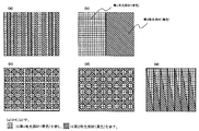
- FIGS. 7-1 to 7-3 show contact surfaces of adjacent light emitting members. On the contact surface, there is a portion where a plurality of types of phosphors overlap in the thickness direction of the fluorescent layer. In this overlapping portion, cascade excitation is very likely to occur. Therefore, the state of FIG. 7-1 is preferable to the state of FIG. 7-2 because cascade excitation can be prevented. Further, it is more preferable that cascade excitation can be further prevented by adopting a configuration as shown in FIG. 7-3 by providing a light shielding portion between the light emitting members.
- the area ratio of the portion where a plurality of the phosphors are present is preferably 10% or less, more preferably 5% or less, and most preferably 0%.
- the area of the overlapping portion where a plurality of types of phosphors overlap is measured by cutting the phosphor layer in the thickness direction and observing the cross section with an electron microscope such as SEM. be able to. Since the phosphor layer of the present invention is manufactured by arranging a plurality of light emitting members, there are a plurality of contact surfaces where the light emitting members are formed adjacent to each other. Therefore, the area of the overlapping portion where a plurality of types of phosphors overlap is represented by the sum of the areas of the overlapping portions existing in the light emission area of the light emitting device of the phosphor layer.
- the first light emitting member and the second light emitting member are preferably disposed as separate members in a direction perpendicular to the thickness direction of the phosphor layer.
- Various modes can be considered for the arrangement.
- examples of the shapes of the first light emitting member and the second light emitting member include a stripe shape, a triangular shape, a quadrangular shape, a hexagonal shape, and a circular shape.
- the first light emitting member and the second light emitting member are preferably arranged as a pattern, and the first light emitting member and the second light emitting member are further arranged in a stripe shape.
- “arranged as a pattern” includes at least one or more first light emitting members and one or more second light emitting members, and the first light emitting member and the second light emitting member are not adjacent to each other.
- “arranged in stripes” means that the first light emitting member and the second light emitting member have the same size and the same shape, and the first member emits light without the same members adjoining each other. The member and the second light emitting member are alternately arranged.
- the first light emitting member and the second light emitting member have a quadrangular shape of the same size and shape, and the same members are not adjacent to each other and are alternately arranged. Is mentioned. Hereinafter, a specific arrangement pattern of the light emitting members will be described.
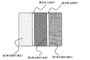
- FIG. 8 shows a first light emitting member including a green phosphor as a phosphor layer and a second light emitting member including a red phosphor when the semiconductor light emitting device emits light having a wavelength in the near ultraviolet or violet region.
- a pattern of a phosphor layer provided with a third light emitting member containing a blue phosphor is shown.
- FIGS. 8A and 8B show a phosphor layer pattern in which rectangular light-emitting members are arranged in stripes, and FIGS. 8C, 8D, and 8E show circular light emission.
- positioned the member is represented, (f) represents the pattern of the fluorescent substance layer which has arrange
- the semiconductor light emitting device when the semiconductor light emitting device emits light having a wavelength in the near ultraviolet or purple region, the first light emitting member including a blue phosphor as the phosphor layer and the second light emitting member including a yellow phosphor are provided.
- the phosphor layer pattern may be used. Such phosphor layer patterns are shown in FIGS. 9A to 9E.
- a phosphor including a first light emitting member including a green phosphor as a phosphor layer and a second light emitting member including a red phosphor may be a layer pattern.
- the pattern in this case is also the pattern shown in FIG. 9 and can be exemplified by a pattern in which the first light emitting member is green and the second light emitting member is red.
- the semiconductor light emitting device when the semiconductor light emitting device emits light having a wavelength in the blue region and a transparent substrate that transmits visible light is used, the semiconductor light emitting device is arranged without arranging the third light emitting member containing the blue phosphor.
- the semiconductor light emitting device is arranged without arranging the third light emitting member containing the blue phosphor.
- FIG. 8 and 9 it can also be set as the pattern which provides a light-shielding part in the interface of each light emitting member.
- FIG. 10 shows a pattern in which a light shielding portion is provided at the interface of each light emitting member in FIG.
- the light shielding part is preferably arranged so as to prevent light emitted from the first light emitting member from entering the second light emitting member. Moreover, it is preferable that a light shielding part is a black matrix or a reflecting material, and it is more preferable that it is a reflecting material. Specific examples of the light shielding part include those obtained by dispersing highly reflective particles in a binder resin.
- the highly reflective particles are preferably alumina particles, titania particles, silica particles, zirconia particles, more preferably alumina particles, titania particles, silica particles, and more preferably alumina particles.
- the semiconductor light emitting device of the present invention emits excitation light of a phosphor contained in the first light emitting member and the second light emitting member.
- the wavelength of the excitation light is 350 nm or more and 520 nm or less, preferably 370 nm or more, more preferably 380 nm or more.
- it is 500 nm or less, More preferably, it is 480 nm or less.
- light emitted from the semiconductor light emitting element be light in the near ultraviolet or violet region because the color rendering properties of the light emitted from the light emitting device can be improved.
- the semiconductor light-emitting device include semiconductor light-emitting devices using InGaAlN-based, GaAlN-based, InGaAlN-based semiconductors, and the like that are crystal-grown on a substrate such as silicon carbide, sapphire, and gallium nitride by a method such as MOCVD. .
- a substrate such as silicon carbide, sapphire, and gallium nitride by a method such as MOCVD.
- MOCVD gallium nitride
- the present invention is preferably used for a light emitting device having such a large light emitting area.
- the light emitting device of the present invention can include a package for holding a semiconductor light emitting element, and its shape and material are arbitrary. As a specific shape, a plate shape, a cup shape, or the like can be used according to the application. Among these, a cup-shaped package is preferable because it can have directivity in the light emission direction and can effectively use light emitted from the light-emitting device. In the case of a cup-shaped package, the area of the opening from which light is emitted is preferably 120% or more and 600% or less of the bottom area.
- the package material an appropriate material such as an inorganic material such as metal, alloy glass or carbon, or an organic material such as synthetic resin can be used.
- a material having a high light reflectance in the near ultraviolet region and the visible light region in general.
- highly reflective packages include those formed of silicone resin and containing light diffusing particles.
- the light diffusing particles include titania and alumina.
- the light-emitting device of the present invention includes a band-pass filter that reflects at least a part of light emitted from the semiconductor light-emitting element and transmits at least a part of light emitted from the phosphor. It is preferable to provide on the exit surface side.
- a bandpass filter that transmits at least part of the excitation light emitted from the semiconductor light emitting element and reflects at least part of the light emitted from the phosphor on the semiconductor light emitting element side of the phosphor layer.
- a metal wiring for supplying electric power from the outside to the semiconductor light emitting element, a cap for protecting the light emission direction side of the phosphor layer, and the like can be appropriately disposed.
- the light-emitting device of the present invention has two or more regions having different emission spectra, for example, an A region and a B region, and the phosphor layer or the semiconductor light-emitting element is a phosphor layer. It is preferable to be configured to move in a direction perpendicular to the thickness direction.
- the A region and the B region of the phosphor layer are regions having different emission spectra of light emitted from the respective regions, and therefore the A region and B occupying the light emission region of the light emitting device.
- the emission spectrum of light emitted from the light emitting device can be continuously adjusted, so that a light emitting device that emits light of a desired emission spectrum can be obtained.
- the A region and the B region are regions having different color temperatures of emitted light
- the light emitted from the light emitting device can be changed by changing the ratio of the A region and the B region in the light emitting region of the light emitting device.
- the color temperature can be continuously adjusted, for example, from 2800K to 6500K.
- the areas of the first light emitting member and the second light emitting member are the same, that is, the patterns are the same.
- the semiconductor light emitting element emits excitation light in the blue region, for example, the same first light emitting member (green) is used for both the A region and the B region, and the second light emitting member used in the A region is included for the second light emitting member.
- the emission spectrum can be changed by including a phosphor of the same color as the phosphor (red) and a different type of phosphor in the second light emitting member used in the B region.
- the emission spectrum can also be changed by changing the content of the phosphor included in the second light emitting member.
- the emission spectrum can be changed.
- the area of the second light emitting member used in the B region can be made larger than the area of the second light emitting member used in the A region.
- the A region and the B region of the fluorescent layer of the present invention are appropriately arranged so that the emission spectra are different. In particular, it is preferable to appropriately arrange the A region and the B region so that the color temperatures of the emitted colors are different.
- a mode in which red and green phosphors are separately applied for a semiconductor light emitting device that emits light in the blue wavelength range A mode in which red, green, and blue phosphors are separately applied for semiconductor light emitting devices that emit light in the near ultraviolet or ultraviolet region, A mode in which blue and yellow phosphors are separately applied for a semiconductor light emitting device that emits light in the near ultraviolet or ultraviolet region, are appropriately combined.
- the phosphor layer of the present invention having such an A region and a B region is designed to be larger than the emission area of the light emitting device, the phosphor layer is moved to move the light emitted from the A region and the B region.
- the ratio of two types of light having different emission spectra can be adjusted. Even if the phosphor layer is not moved, the emission spectrum can be adjusted by moving the semiconductor light emitting element (or the package in the case of having a package).
- the movement direction may be linear movement or rotational movement.
- the present invention will be described with reference to embodiments of the light emitting device of the present invention.
- the present invention is not limited to the following embodiments, and may be arbitrarily modified and implemented without departing from the gist of the present invention. can do.
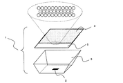
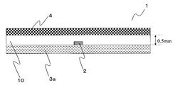
- the light-emitting device 1 is a light-emitting device in which a semiconductor light-emitting element 2 is arranged on a plane, and the semiconductor light-emitting element 2 is arranged on the bottom surface of the recess of the package 3.
- a phosphor layer 4 is disposed in the opening of the package 3.
- the semiconductor light emitting device 2 may be a near ultraviolet semiconductor light emitting device that emits light having a wavelength in the near ultraviolet region, a purple semiconductor light emitting device that emits light in the purple region, or a blue semiconductor light emitting device that emits light in the blue region.
- a purple semiconductor light emitting element will be described as an example.
- one semiconductor light emitting element may be disposed (FIG. 1), or a plurality of semiconductor light emitting elements may be disposed in a planar shape (FIG. 2). It is also possible to arrange one semiconductor light emitting element having a large output to form a light emitting device. In particular, it is preferable to arrange a plurality of semiconductor light-emitting elements in a planar shape or to arrange one semiconductor light-emitting element having a large output because surface illumination can be easily achieved.
- the package 3 holds the semiconductor light emitting element and the phosphor layer.
- the package 3 has a cup shape having an opening and a recess, and the semiconductor light emitting element 2 is disposed on the bottom surface of the recess.
- the dimension of the recessed part of the package 3 is set to such a dimension that the light emitting device 1 can emit light in a predetermined direction.
- an electrode (not shown) for supplying power to the semiconductor light emitting element from the outside of the light emitting device 1 is provided at the bottom of the recess of the package 3.
- the package 3 is preferably a highly reflective package, so that light hitting the wall surface (tapered portion) of the package 3 can be emitted in a predetermined direction, and loss of light can be prevented.
- the phosphor layer 4 is disposed in the opening of the package 3.
- the opening of the recess of the package 3 is covered with the phosphor layer 4, and light from the semiconductor light emitting element 2 does not pass through the phosphor layer 4 and is not emitted from the light emitting device 1.
- the phosphor layer 4 is formed on a transparent substrate 5 that transmits near-ultraviolet light and visible light.
- a transparent substrate 5 that transmits near-ultraviolet light and visible light.
- the phosphor layer 4 formed on the transparent substrate is a layer having a thickness of 1 mm or less.
- the distance between the semiconductor light emitting element 2 and the phosphor layer 4 is long, and the distance is preferably 0.1 mm or more, more preferably 0.3 mm or more, and 0 0.5 mm or more is more preferable, 1 mm or more is particularly preferable, 500 mm or less is preferable, 300 mm or less is more preferable, 100 mm or less is further preferable, and 10 mm or less is particularly preferable.
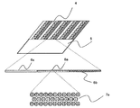
- FIG. 3 shows an embodiment in which the phosphor layer 4 includes first to third light emitting members 6a to 6c.
- the first light emitting member 6a is a light emitting member including the green phosphor 7a.
- the first light emitting member 6a is excited by the light of the purple semiconductor light emitting element 2 and has a longer wavelength component than the light in the purple region.
- the second light emitting member 6b is a light emitting member including a red phosphor, and is excited by the light of the purple semiconductor light emitting element 2 to emit light in the green region emitted from the green phosphor included in the first light emitting member. It emits light in the red region, which is a longer wavelength component.
- the third light emitting member 6c is a light emitting member including a blue phosphor, and is provided for generating white light.
- each light emitting member is appropriately selected according to the type of the semiconductor light emitting element to be used.
- the third light emitting member is not necessary, and the light from the blue semiconductor light emitting element is generated to generate white light. It can be used as it is as blue light.
- each light emitting member has an area where a plurality of types of phosphors exist in the thickness direction of the phosphor layer with respect to the light emission area of the phosphor layer in the light emitting device, that is, the area of the opening of the package 3. And 0% or more and 20% or less. Since there are a plurality of light emitting members in the light emission area, the area of a portion where a plurality of types of phosphors exist is calculated as the sum of the areas of the plurality of portions.
- a band-pass filter 9 can be provided on the light emitting surface side of the phosphor layer 4 and / or the semiconductor light emitting element side.
- the “light emitting surface side of the light emitting device of the phosphor layer 4” is the surface of the surface perpendicular to the thickness direction of the phosphor layer 4 that emits light to the outside of the light emitting device. In other words, when referring to FIG. 4, it means above the phosphor layer 4.
- the “semiconductor light emitting element side of the phosphor layer 4” means the side of the surface that emits light into the light emitting device among the surfaces perpendicular to the thickness direction of the phosphor layer 4, that is, If it demonstrates using FIG.
- the band-pass filter 9 has a property of transmitting only light having a predetermined wavelength, transmits at least part of light emitted from the semiconductor light emitting element, and reflects at least part of light emitted from the phosphor.
- the pass filter between the package 3 and the phosphor layer 4 the fluorescence emitted from the phosphor can be prevented from entering the package again, and the light emission efficiency of the light emitting device can be improved.
- a band pass filter that reflects at least part of light emitted from the semiconductor light emitting element and transmits at least part of light emitted from the phosphor is provided on the light emitting surface side of the light emitting device of the phosphor layer 4.
- the light emitted from the semiconductor light emitting element that has passed without being absorbed by the phosphor can be returned again to the phosphor layer to excite the phosphor, and the luminous efficiency of the light emitting device can be increased.
- the band pass filter is appropriately selected according to the semiconductor light emitting element 2. Also, as shown in FIG. 4, by arranging a plurality of semiconductor light emitting elements in a planar shape, it is possible to increase the proportion of light incident in the thickness direction of the bandpass filter out of the light emitted from the semiconductor light emitting elements.
- the bandpass filter can be used more efficiently.
- the phosphor layer 4 has two regions of different emission spectra, for example, an A region 4a and a B region 4b having different color temperatures, and the size of the phosphor layer 4 is It is designed to be larger than the size of the opening of the package 3. Then, the phosphor layer 4 having a larger area than the opening of the package 3 is horizontally slid while covering the opening of the package 3 (arrow 8 in the figure is an example of the horizontal sliding direction of the phosphor layer 4). It is possible to adjust the color temperature of the white light emitted from the light emitting device 1 by adjusting the ratio of the light emitted from the semiconductor light emitting element 2 to the A region and the B region. It is also possible to slide the package 3 horizontally without sliding the phosphor layer 4 horizontally.
- the A region 4a of the phosphor layer is a high color temperature region where the color temperature of the emission color is 6500K
- the B region 4b is a low color temperature region where the color temperature of the emission color is 2800K
- the areas of the A region and the B region are In the light emitting device 1 having the same area as the opening of the package, pale white light having a color temperature of 6500K is emitted when the opening of the package 3 is entirely covered with the A region 4a of the phosphor layer.
- white light having a color temperature of about 4600K, which is between 2800K and 6500K is emitted.
- FIG. 6 shows a schematic diagram of another embodiment of the arrangement of the semiconductor light emitting element 2, the package 3, and the phosphor layer 4.
- FIG. 6A shows the embodiment of FIG. 1 in which the phosphor layer 4 is disposed in the opening of the package 3.
- the phosphor layer 4 or the package 3 is installed so that it can move in the direction of the arrow.
- the light emitted from the semiconductor light emitting element 2 becomes fluorescent in the phosphor layer 4 and is emitted outside the apparatus.
- FIG. 6B shows a form in which the periphery of the semiconductor light emitting element 2 is arranged so as to be covered with the phosphor layer 4.
- the phosphor layer 4 can be moved in the direction of the arrow, and the package 3 can be moved in the direction of the arrow.
- FIG. 6C shows a form in which the phosphor layer 4 is disposed on the surface of the package 3, and the semiconductor light emitting element 2 is held by a translucent member provided in the opening and disposed so as to emit light downward in the drawing. is there.
- the phosphor layer 4 can be moved in the direction of the arrow along the shape of the recess of the package 3, and the semiconductor light emitting element 2 is installed so as to be moved in the direction of the arrow.
- the light emitted from the semiconductor light emitting element 2 becomes fluorescent in the phosphor layer 4, and the fluorescent light is reflected by the package 3 including a reflective material and emitted outside the apparatus.
- the distance between the semiconductor light emitting element 2 and the phosphor layer 4 is long, and the distance is preferably 0.1 mm or more, more preferably 0.3 mm or more, and 0.5 mm or more. Is more preferably 1 mm or more, preferably 500 mm or less, more preferably 300 mm or less, further preferably 100 mm or less, and particularly preferably 50 mm or less.
- the excitation light per fluorescent substance unit area can be weakened and the photodegradation of fluorescent substance can be prevented.
- the present invention will be described more specifically with reference to experimental examples.
- the present invention is not limited to the following experimental examples, and may be arbitrarily modified and implemented without departing from the scope of the present invention.
- Can do the measurement of the particle diameter and particle size distribution of the phosphor, the measurement of the thickness of the phosphor layer, and the measurement of the emission spectrum of the light emitting device in the experimental example were performed by the following methods.
- the volume average median diameter D 50v was obtained from the particle diameter value when the integrated value calculated from the intensity of the frequency-based particle size distribution curve was 50%.
- the frequency-based particle size distribution curve was able to measure the particle size distribution by a laser diffraction / scattering method. Specifically, a phosphor is placed in ultrapure water, and using an ultrasonic disperser (manufactured by Kaijo Co., Ltd.), the frequency is 19 KHz, the ultrasonic intensity is 5 W, and the sample is ultrasonically dispersed for 25 seconds.
- a laser diffraction particle size distribution analyzer (Horiba) It was possible to measure in a particle size range of 0.1 ⁇ m to 600 ⁇ m with a mill LA-300).
- the volume-based average particle diameter D v is calculated from the frequency-based particle size distribution curve by the formula ⁇ (v / d) / ⁇ v
- the number-based average particle diameter D n is calculated from the frequency-based particle size distribution curve by ⁇ It calculated from the calculation formula of (v / d 2 ) / ⁇ (v / d 3 ).
- d is a representative value of each particle size channel
- v is a volume-based percentage for each channel.
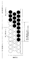
- Measurement of phosphor layer thickness For the thickness of the phosphor layer, measure the total thickness of the phosphor layer and the substrate coated with the phosphor layer with a micrometer, and measure the thickness of the substrate after peeling the phosphor layer from the substrate. Calculated with In addition, the difference between the maximum value and the minimum value of the thickness was calculated by measuring film thicknesses at arbitrary four different points.
- CSMS phosphors having a peak wavelength represented by Ca 3 (Sc, Mg) 2 Si 3 O 12 : Ce of 514 nm (volume-based median diameter: 12 ⁇ m) and (Sr , Ca) AlSiN 3 : SCASN phosphor having a peak wavelength represented by 630 nm (volume-based median diameter: 10 ⁇ m) is used, and a silicone resin (Toray Dow Corning Co., Ltd.) is used as the binder resin used in the phosphor layer.
- a silicone resin Toray Dow Corning Co., Ltd.
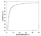
- FIG. 12 shows a simulation result of the value of the total luminous flux when the volume filling factor of the phosphor in the phosphor layer is changed. As is apparent from FIG. 12, the total luminous flux increases rapidly as the volume filling rate increases in the range of 2% to 7%, whereas the volume increases in the range of 7% to 15%.
- the total luminous flux gradually increases as the filling factor increases, and the total luminous flux hardly increases as the volume filling factor increases at 15% or more, particularly 20% or more. That is, if the volume filling rate is 15% or more, particularly 20% or more, it is possible to suppress the influence of light absorption by the sealing resin to the maximum, and the light emission efficiency of the light emitting device can be improved.
- a light emitting device including a semiconductor light emitting element module and a phosphor layer was produced, and the total luminous flux thereof was measured.
- Cavity bottom surface of 3528SMD type PPA resin package by using a silicon resin-based transparent die-bond paste as an InGaN-based LED chip of 350 ⁇ m square and main emission peak wavelength 405 nm formed using a sapphire substrate as a semiconductor light emitting device module Glued on top. After bonding, the die bond paste was cured by heating at 150 ° C. for 2 hours, and then the LED chip-side electrode and the package-side electrode were connected using an Au wire having a diameter of 25 ⁇ m.
- the phosphor, Sr 5-b Ba b ( PO 4) 3 Cl: peak wavelength represented by Eu is 450 nm SBCA phosphor (volume-based median diameter D 50v: 11 ⁇ m, D v / D n 1.
- GLS-HF polyester urethane resin
- the phosphor layer is prepared by first putting a predetermined amount of the binder resin and the three types of phosphors in the same container, and mixing and stirring them with Awatori Nertaro (Sinky Corporation). It was produced by applying a plurality of times onto a PET resin having a thickness of 100 ⁇ m using ST-310F1G), and drying it by heating at 150 ° C. for 30 minutes to solidify the resin.
- the light emitting surface (opening portion of the package) of the semiconductor light emitting device module and the phosphor layer are in close contact, and the upper surface of the semiconductor light emitting device and the lower surface of the phosphor layer are spaced apart by a distance of 0.85 mm.
- a light emitting device was manufactured.
- the space between the phosphor layer and the semiconductor light emitting element was an air layer. Table 1 shows values of various emission characteristics (chromaticity coordinates (Cx, Cy), correlated color temperature, total luminous flux) calculated from the obtained emission spectrum.
- Example 3 A light emitting device including a semiconductor light emitting module and a phosphor layer was produced in the same manner as in Experimental Example 2 except that the phosphor content in the phosphor layer was 21% by volume filling rate, and the light emission was performed. The spectrum was measured. Table 1 shows values of various emission characteristics (chromaticity coordinates (Cx, Cy), correlated color temperature, total luminous flux) calculated from the obtained emission spectrum.
- Example 4 A light emitting device including a semiconductor light emitting module and a phosphor layer was produced in the same manner as in Experimental Example 3 except that the phosphor content in the phosphor layer was 12% in volume filling ratio, and the light emission was performed. The spectrum was measured. Table 1 shows values of various emission characteristics (chromaticity coordinates (Cx, Cy), correlated color temperature, total luminous flux) calculated from the obtained emission spectrum. The values of the total luminous flux obtained in Experimental Examples 2 to 4 are relative values when the numerical value obtained in Experimental Example 4 is set to 100.
- a phosphor layer having a high volume filling rate can be produced.
- the number of peaks in the frequency standard particle size distribution curve of the phosphor mixture was one.
- Example 6 A light emitting device including a semiconductor light emitting module and a phosphor layer was produced in the same manner as in Experimental Example 5 except that the number of times of application onto the PET resin was changed to 2, and the total luminous flux thereof was measured.
- Example 7 A light emitting device including a semiconductor light emitting module and a phosphor layer was produced in the same manner as in Experimental Example 5 except that the number of times of application onto the PET resin was changed to 3, and the total luminous flux thereof was measured.
- Example 8 A light emitting device including a semiconductor light emitting module and a phosphor layer was produced in the same manner as in Experimental Example 5 except that the number of times of application onto the PET resin was changed to 4, and the total luminous flux thereof was measured.
- Example 9 A light emitting device including a semiconductor light emitting module and a phosphor layer was produced in the same manner as in Experimental Example 5 except that the number of times of application onto the PET resin was changed to 5, and the total luminous flux thereof was measured.
- Example 10 A light emitting device including a semiconductor light emitting module and a phosphor layer was produced in the same manner as in Experimental Example 5 except that the number of coatings on the PET resin was changed to 6, and the total luminous flux thereof was measured.
- Example 11 A light emitting device including a semiconductor light emitting module and a phosphor layer was prepared in the same manner as in Experimental Example 5 except that the number of times of application onto the PET resin was set to 7, and the emission spectrum thereof was measured.
- Example 12 A light emitting device including a semiconductor light emitting module and a phosphor layer was produced in the same manner as in Experimental Example 5 except that the number of times of application onto the PET resin was changed to 8, and the emission spectrum was measured.
- Table 2 and FIG. 13 show the values of the emission characteristics (total luminous flux) and the average layer thickness calculated from the obtained emission spectrum.
- the present invention can be used in the field where light is used, and can be suitably used for, for example, indoor and outdoor lighting.
- the present invention has been described by exemplifying specific embodiments, those skilled in the art can easily understand that the embodiments can be changed without departing from the scope of the present invention.
Abstract
Disclosed is a light-emitting device wherein self-absorption of light among phosphors is reduced, the light-emitting efficiency of the phosphors is increased by reducing the absorption of fluorescence by a sealing resin, and wherein optical scattering of the phosphor is prevented and the light extraction efficiency from a phosphor layer is increased. The disclosed light-emitting device is configured to have a semiconductor light-emitting element and a phosphor layer, the phosphor layer being a compact phosphor layer wherein the particle size distribution of the phosphor contained in said layer, and the filling ratio of the phosphor contained in said layer are specified values.
Description
本発明は、発光装置、特に、発光効率が高く、かつ、光取り出し効率の高い蛍光体層を備える発光装置に関する。
The present invention relates to a light emitting device, and more particularly, to a light emitting device including a phosphor layer having high light emission efficiency and high light extraction efficiency.
半導体発光素子を用いた発光装置は、発光素子を覆う封止樹脂中に蛍光体を保持させ、発光素子から照射された光を蛍光体で色変換して外部に照射している。例えば特許文献1では、蛍光体と封止樹脂とを含む蛍光体層を備える発光装置において、蛍光体層の膜厚と、その中に含まれる蛍光体の充填率を特定の値とすることで、半導体発光素子を電気的に接続しているボンディングワイヤの断線を防止できることが記載されている。
In a light emitting device using a semiconductor light emitting element, a phosphor is held in a sealing resin covering the light emitting element, and the light emitted from the light emitting element is color-converted by the phosphor and radiated to the outside. For example, in Patent Document 1, in a light emitting device including a phosphor layer including a phosphor and a sealing resin, the film thickness of the phosphor layer and the filling rate of the phosphor contained therein are set to specific values. Further, it is described that it is possible to prevent disconnection of a bonding wire that electrically connects a semiconductor light emitting element.
しかしながら、特許文献1に記載の発光装置は、厚みの大きい蛍光体層を用いていることにより、蛍光体層の中でも半導体発光素子に近い位置に配置された蛍光体から発せられた蛍光のうち、光射出面に到達するまでに同種類の蛍光体によって自己吸収される割合が多く、また、光出射面に到達するまでに封止樹脂によって吸収される割合が多く、その結果、蛍光体層の発光効率が低くなるという課題があった(第1の課題)。
また、厚みの大きい蛍光体層を用いていることにより、蛍光体層の中でも半導体発光素子に近い位置に配置された蛍光体から発せられた蛍光のうち、光射出面に到達するまでに他の蛍光体によって散乱される割合が多く、その結果、蛍光体層における光取り出し効率が低くなるという課題があった(第2の課題)。
また、蛍光体層中に発光色の異なる複数の蛍光体を混合して含有させた場合には、ある一種の蛍光体が発した蛍光を他種の蛍光体が吸収する現象、いわゆるカスケード励起が起こり、蛍光体層の発光効率が低くなるという課題があった(第3の課題)。
さらに、特許文献1に記載の発光装置のように、蛍光体層が半導体発光素子を直接覆うように構成した場合には、半導体発光素子の光出力が高くなるにつれて、半導体発光素子の温度が上昇するだけでなく、蛍光体での色変換の際の損失によって発生する熱で蛍光体の温度も上昇し、その結果、半導体発光素子及び蛍光体層の発光効率が低くなるという課題があった(第4の課題)。
また、紫外光から近紫外光に発光する半導体発光素子と、前記半導体発光素子からの光によって励起されて可視光を発する蛍光体を用いて発光装置を構成した場合には、前記半導体発光素子からの光のうち、蛍光体層で可視光に変換されずにそのまま出力される光の割合が多くなると、蛍光体層の発光効率が低くなるという課題があった(第5の課題)。
さらに、紫外光から近紫外光に発光する半導体発光素子と、前記半導体発光素子からの光によって励起されて可視光を発する蛍光体を用いて発光装置を構成した場合には、蛍光体層から発せられる可視光のうち、半導体発光素子側に射出される光の割合が多くなると、発光装置の発光効率が低くなるという課題があった(第6の課題)。
また、特許文献1に記載の発光装置のように、蛍光体層が半導体発光素子を直接覆うようにした場合は、蛍光体層や半導体発光素子の位置を動かしたり、それらを取り外して交換できるような構成としない限りは、容易に発光装置の発光スペクトルを変えることができないという課題があった(第7の課題)。 However, the light-emitting device described inPatent Document 1 uses a phosphor layer having a large thickness, so that among the phosphors emitted from phosphors arranged at positions close to the semiconductor light-emitting element among the phosphor layers, The ratio of self-absorption by the same type of phosphor before reaching the light emission surface is large, and the ratio of absorption by the sealing resin until it reaches the light emission surface is large. There has been a problem that the luminous efficiency is low (first problem).
In addition, by using a phosphor layer with a large thickness, among the phosphors emitted from the phosphors arranged at positions close to the semiconductor light emitting element among the phosphor layers, other phosphors are required before reaching the light exit surface. There is a large proportion of the light scattered by the phosphor, and as a result, there is a problem that the light extraction efficiency in the phosphor layer is low (second problem).
In addition, when a plurality of phosphors with different emission colors are mixed and contained in the phosphor layer, a phenomenon in which the fluorescence emitted by one type of phosphor is absorbed by another type of phosphor, so-called cascade excitation, occurs. This occurred and there was a problem that the luminous efficiency of the phosphor layer was lowered (third problem).
Further, when the phosphor layer is configured to directly cover the semiconductor light emitting element as in the light emitting device described inPatent Document 1, the temperature of the semiconductor light emitting element increases as the light output of the semiconductor light emitting element increases. In addition, the temperature of the phosphor also rises due to the heat generated by the loss during color conversion in the phosphor, and as a result, there is a problem that the luminous efficiency of the semiconductor light emitting device and the phosphor layer is lowered ( Fourth problem).
When a light emitting device is configured using a semiconductor light emitting element that emits light from ultraviolet light to near ultraviolet light and a phosphor that emits visible light when excited by light from the semiconductor light emitting element, the semiconductor light emitting element When the ratio of the light that is output as it is without being converted into visible light by the phosphor layer increases, the luminous efficiency of the phosphor layer decreases (fifth problem).
Furthermore, when a light emitting device is configured using a semiconductor light emitting device that emits light from ultraviolet light to near ultraviolet light and a phosphor that emits visible light when excited by light from the semiconductor light emitting device, the light emitting device emits light from the phosphor layer. When the ratio of the light emitted to the semiconductor light emitting element side in the visible light generated increases, there is a problem that the light emission efficiency of the light emitting device decreases (sixth problem).
Further, when the phosphor layer directly covers the semiconductor light emitting element as in the light emitting device described inPatent Document 1, the positions of the phosphor layer and the semiconductor light emitting element can be moved, or they can be removed and replaced. As long as the configuration is not different, there is a problem that the emission spectrum of the light emitting device cannot be easily changed (seventh problem).
また、厚みの大きい蛍光体層を用いていることにより、蛍光体層の中でも半導体発光素子に近い位置に配置された蛍光体から発せられた蛍光のうち、光射出面に到達するまでに他の蛍光体によって散乱される割合が多く、その結果、蛍光体層における光取り出し効率が低くなるという課題があった(第2の課題)。
また、蛍光体層中に発光色の異なる複数の蛍光体を混合して含有させた場合には、ある一種の蛍光体が発した蛍光を他種の蛍光体が吸収する現象、いわゆるカスケード励起が起こり、蛍光体層の発光効率が低くなるという課題があった(第3の課題)。
さらに、特許文献1に記載の発光装置のように、蛍光体層が半導体発光素子を直接覆うように構成した場合には、半導体発光素子の光出力が高くなるにつれて、半導体発光素子の温度が上昇するだけでなく、蛍光体での色変換の際の損失によって発生する熱で蛍光体の温度も上昇し、その結果、半導体発光素子及び蛍光体層の発光効率が低くなるという課題があった(第4の課題)。
また、紫外光から近紫外光に発光する半導体発光素子と、前記半導体発光素子からの光によって励起されて可視光を発する蛍光体を用いて発光装置を構成した場合には、前記半導体発光素子からの光のうち、蛍光体層で可視光に変換されずにそのまま出力される光の割合が多くなると、蛍光体層の発光効率が低くなるという課題があった(第5の課題)。
さらに、紫外光から近紫外光に発光する半導体発光素子と、前記半導体発光素子からの光によって励起されて可視光を発する蛍光体を用いて発光装置を構成した場合には、蛍光体層から発せられる可視光のうち、半導体発光素子側に射出される光の割合が多くなると、発光装置の発光効率が低くなるという課題があった(第6の課題)。
また、特許文献1に記載の発光装置のように、蛍光体層が半導体発光素子を直接覆うようにした場合は、蛍光体層や半導体発光素子の位置を動かしたり、それらを取り外して交換できるような構成としない限りは、容易に発光装置の発光スペクトルを変えることができないという課題があった(第7の課題)。 However, the light-emitting device described in
In addition, by using a phosphor layer with a large thickness, among the phosphors emitted from the phosphors arranged at positions close to the semiconductor light emitting element among the phosphor layers, other phosphors are required before reaching the light exit surface. There is a large proportion of the light scattered by the phosphor, and as a result, there is a problem that the light extraction efficiency in the phosphor layer is low (second problem).
In addition, when a plurality of phosphors with different emission colors are mixed and contained in the phosphor layer, a phenomenon in which the fluorescence emitted by one type of phosphor is absorbed by another type of phosphor, so-called cascade excitation, occurs. This occurred and there was a problem that the luminous efficiency of the phosphor layer was lowered (third problem).
Further, when the phosphor layer is configured to directly cover the semiconductor light emitting element as in the light emitting device described in
When a light emitting device is configured using a semiconductor light emitting element that emits light from ultraviolet light to near ultraviolet light and a phosphor that emits visible light when excited by light from the semiconductor light emitting element, the semiconductor light emitting element When the ratio of the light that is output as it is without being converted into visible light by the phosphor layer increases, the luminous efficiency of the phosphor layer decreases (fifth problem).
Furthermore, when a light emitting device is configured using a semiconductor light emitting device that emits light from ultraviolet light to near ultraviolet light and a phosphor that emits visible light when excited by light from the semiconductor light emitting device, the light emitting device emits light from the phosphor layer. When the ratio of the light emitted to the semiconductor light emitting element side in the visible light generated increases, there is a problem that the light emission efficiency of the light emitting device decreases (sixth problem).
Further, when the phosphor layer directly covers the semiconductor light emitting element as in the light emitting device described in
本発明者らは、上記第1の課題及び第2の課題を解決すべく鋭意研究を重ね、発光装置に備える蛍光体層の構成に着目した。そして、蛍光体層の厚さと蛍光体層に含まれる蛍光体の充填率を特定の値とした薄くて緻密な蛍光体層を用いることで、蛍光体同士の光の自己吸収を減少させ蛍光体の発光効率を高めることができ、さらに蛍光体の光散乱を防止し蛍光体層からの光の取り出し効率を高めることができることを見出し、発明を完成させた。本発明は、
半導体発光素子と、蛍光体層とを有して構成される発光装置であって、
(i)前記半導体発光素子は350nm以上520nm以下の波長を有する光を発し、
(ii)前記蛍光体層は、前記半導体発光素子が発する光によって励起されて、前記半導体発光素子が発する光よりも長波長の成分を含む光を発しうる蛍光体を含み、
(iii)前記蛍光体層は、前記蛍光体を体積充填率で15%以上含有しており、
(iv)前記蛍光体層において、前記蛍光体の体積基準の平均粒子径Dvと個数基準の平均粒子径Dnの比(Dv/Dn)が1.2以上25以下である
ことを特徴とする発光装置である。 The inventors of the present invention have made extensive studies to solve the first and second problems, and have focused on the structure of the phosphor layer provided in the light emitting device. And, by using a thin and dense phosphor layer with a specific value for the thickness of the phosphor layer and the filling rate of the phosphor contained in the phosphor layer, the self-absorption of light between the phosphors is reduced and the phosphor The present inventors have found that the light emission efficiency of the phosphor can be increased, the light scattering efficiency of the phosphor can be prevented, and the light extraction efficiency from the phosphor layer can be enhanced. The present invention
A light-emitting device configured to include a semiconductor light-emitting element and a phosphor layer,
(I) The semiconductor light emitting device emits light having a wavelength of 350 nm or more and 520 nm or less,
(Ii) The phosphor layer includes a phosphor that is excited by light emitted from the semiconductor light emitting element and can emit light including a component having a longer wavelength than the light emitted from the semiconductor light emitting element.
(Iii) The phosphor layer contains the phosphor in a volume filling ratio of 15% or more,
(Iv) In the phosphor layer, a ratio (D v / D n ) between the volume-based average particle diameter Dv and the number-based average particle diameter D n of the phosphor is 1.2 or more and 25 or less. Is a light emitting device.
また、前記蛍光体層は、前記蛍光体の体積基準のメディアン径D50vの2倍以上10倍以下の厚さを有していることが好ましい態様である。
Moreover, it is a preferable aspect that the phosphor layer has a thickness of 2 to 10 times the volume-based median diameter D 50v of the phosphor.
また、前記蛍光体は、前記体積基準のメディアン径D50vが2μm以上30μm以下であることが好ましい態様である。
In addition, the phosphor preferably has a volume-based median diameter D 50v of 2 μm or more and 30 μm or less.
また、本発明は、
半導体発光素子と、蛍光体層とを有して構成される発光装置であって、
(i)前記半導体発光素子は350nm以上520nm以下の波長を有する光を発し、
(ii)前記蛍光体層は、前記半導体発光素子が発する光によって励起されて、前記半導体発光素子が発する光よりも長波長光を発しうる蛍光体を含み、
(iii)前記蛍光体層は、前記蛍光体の体積基準のメディアン径D50vの2倍以上10倍以下の厚さを有しており、
(iv)前記蛍光体層において、前記蛍光体の体積基準の平均粒子径Dvと個数基準の平均粒子径Dnの比(Dv/Dn)が1.2以上25以下である
ことを特徴とする発光装置である。 The present invention also provides:
A light-emitting device configured to include a semiconductor light-emitting element and a phosphor layer,
(I) The semiconductor light emitting device emits light having a wavelength of 350 nm or more and 520 nm or less,
(Ii) The phosphor layer includes a phosphor that is excited by light emitted from the semiconductor light emitting element and can emit light having a longer wavelength than light emitted from the semiconductor light emitting element;
(Iii) The phosphor layer has a thickness of 2 to 10 times the volume-based median diameter D 50v of the phosphor,
(Iv) In the phosphor layer, a ratio (D v / D n ) between the volume-based average particle diameter Dv and the number-based average particle diameter D n of the phosphor is 1.2 or more and 25 or less. Is a light emitting device.
また、前記蛍光体層は、最大厚さ及び最小厚さの差が、前記蛍光体層の体積基準のメディアン径D50v以下であることが好ましい態様である。
Further, in the phosphor layer, a difference between the maximum thickness and the minimum thickness is preferably a volume-based median diameter D 50v or less of the phosphor layer.
また、本発明は、半導体発光素子と、蛍光体層とを有して構成される発光装置であって、
(i)前記半導体発光素子は350nm以上520nm以下の波長を有する光を発し、
(ii)前記蛍光体層は、前記半導体発光素子が発する光によって励起されて、前記半導体発光素子が発する光よりも長波長光を発しうる蛍光体を含み、
(iii)前記蛍光体層において、前記蛍光体の体積基準の平均粒子径Dvと個数基準の平均粒子径Dnの比(Dv/Dn)が1.2以上25以下であり、
(iv)前記蛍光体層は、最大厚さ及び最小厚さの差が、前記蛍光体層の体積基準のメディアン径D50v以下である
ことを特徴とする発光装置である。 Further, the present invention is a light emitting device comprising a semiconductor light emitting element and a phosphor layer,
(I) The semiconductor light emitting device emits light having a wavelength of 350 nm or more and 520 nm or less,
(Ii) The phosphor layer includes a phosphor that is excited by light emitted from the semiconductor light emitting element and can emit light having a longer wavelength than light emitted from the semiconductor light emitting element;
(Iii) In the phosphor layer, a ratio (D v / D n ) of the volume-based average particle diameter D v and the number-based average particle diameter D n of the phosphor is 1.2 or more and 25 or less,
(Iv) The phosphor layer is a light emitting device characterized in that the difference between the maximum thickness and the minimum thickness is not more than the volume-based median diameter D 50v of the phosphor layer.
また、前記蛍光体層は、バインダー樹脂を含むことが好ましい態様である。
In addition, it is preferable that the phosphor layer includes a binder resin.
また、前記蛍光体は、発光スペクトルにおける発光波長領域と、励起スペクトルにおける励起波長領域とで波長範囲が重複していることが好ましい態様である。
Moreover, it is a preferable aspect that the phosphors have overlapping wavelength ranges in the emission wavelength region in the emission spectrum and the excitation wavelength region in the excitation spectrum.
また、前記蛍光体は、前記半導体発光素子が発する光により励起されて前記半導体発光素子が発する光よりも長波長の第1の光を発しうる第1の蛍光体と、前記半導体発光素子が発する光により励起されて前記第1の光よりも長波長の第2の光を発しうる第2の蛍光体とを含有することが好ましい態様である。
In addition, the phosphor is excited by light emitted from the semiconductor light emitting element, and the semiconductor light emitting element emits a first phosphor that can emit first light having a longer wavelength than light emitted from the semiconductor light emitting element. It is a preferable aspect that it contains a second phosphor that is excited by light and can emit second light having a longer wavelength than the first light.
また、前記第2の蛍光体は、前記第1の光により励起されて前記第1の光よりも長波長の第2の光を発しうる蛍光体であることが好ましい態様である。
Further, it is preferable that the second phosphor is a phosphor that is excited by the first light and can emit second light having a longer wavelength than the first light.
また、前記第1の蛍光体のD50vの値と、前記第2の蛍光体のD50vの値との差が1μm以上であることが好ましい態様である。
Further, the value of D 50v of the first phosphor, it is preferred embodiment the difference between the value of D 50v of the second phosphor is 1μm or more.
また、第3の課題を解決するには、前記蛍光体層は第1発光部材及び第2発光部材を備え、
(i)前記第1発光部材は、前記第1の蛍光体を含有し、
(ii)前記第2発光部材は、前記第2の蛍光体を含有し、
(iii)前記蛍光体層において第1発光部材及び第2発光部材は、蛍光体層の厚さ方向に対して垂直の方向に、各々別の部材として形成されていることが好ましい態様である。 In order to solve the third problem, the phosphor layer includes a first light emitting member and a second light emitting member,
(I) The first light emitting member contains the first phosphor,
(Ii) The second light emitting member contains the second phosphor,
(Iii) In the phosphor layer, the first light emitting member and the second light emitting member are preferably formed as separate members in a direction perpendicular to the thickness direction of the phosphor layer.
また、第4の課題を解決するには、前記発光装置は、前記半導体発光素子と前記蛍光体層との間の距離を0.1mm以上500mm以下とすることが好ましい態様である。
In order to solve the fourth problem, it is preferable that the light emitting device has a distance between the semiconductor light emitting element and the phosphor layer of 0.1 mm to 500 mm.
また、第5の課題を解決するには、前記発光装置は、前記半導体発光素子が発する光の少なくとも一部を反射し、かつ、前記蛍光体が発する光の少なくとも一部を透過するバンドパスフィルターを、前記蛍光体層の発光装置の光の射出面側に備えることが好ましい態様である。
In order to solve the fifth problem, the light-emitting device reflects at least part of light emitted from the semiconductor light-emitting element and transmits at least part of light emitted from the phosphor. Is preferably provided on the light emitting surface side of the light emitting device of the phosphor layer.
また、第6の課題を解決するには、前記発光装置は、前記半導体発光素子が発する光の少なくとも一部を透過し、かつ、前記蛍光体が発する光の少なくとも一部を反射するバンドパスフィルターを、前記蛍光体層の前記半導体発光素子側に備えることが好ましい態様である。
In order to solve the sixth problem, the light-emitting device transmits at least part of light emitted from the semiconductor light-emitting element and reflects at least part of light emitted from the phosphor. Is preferably provided on the semiconductor light emitting element side of the phosphor layer.
また、第7の課題を解決するには、前記蛍光体層は発光スペクトルが異なるA領域とB領域とを含み、前記発光装置は、前記蛍光体層又は前記半導体発光素子が蛍光体層の厚さ方向に対して垂直の方向に移動することで、前記半導体発光素子からA領域及びB領域に照射される光の割合を調整することが可能であることが好ましい態様である。
In order to solve the seventh problem, the phosphor layer includes an A region and a B region having different emission spectra, and the light-emitting device has a thickness of the phosphor layer or the semiconductor light-emitting element. It is a preferable aspect that it is possible to adjust the ratio of light emitted from the semiconductor light emitting element to the A region and the B region by moving in a direction perpendicular to the vertical direction.
本発明により、蛍光体同士の光の自己吸収及び封止樹脂による光の吸収を減少させ蛍光体の発光効率を高め、さらに蛍光体の光散乱を防止し蛍光体層からの光の取り出し効率を高めた発光装置を提供することができる。
According to the present invention, the self-absorption of light between phosphors and the absorption of light by the sealing resin are reduced to increase the light emission efficiency of the phosphor, and further, the light scattering of the phosphor is prevented and the light extraction efficiency from the phosphor layer is increased. An enhanced light-emitting device can be provided.
本発明の発光装置は、半導体発光素子、および蛍光体層を有する発光装置である。また、通常発光装置は、半導体発光素子を保持するためのパッケージを備える。
The light emitting device of the present invention is a light emitting device having a semiconductor light emitting element and a phosphor layer. The normal light emitting device includes a package for holding the semiconductor light emitting element.
<1.蛍光体層>
<1-1.蛍光体層の特性>
本発明の発光装置が備える蛍光体層は、蛍光体を含み、緻密に形成した蛍光体層であることが好ましい。 <1. Phosphor layer>
<1-1. Characteristics of phosphor layer>
The phosphor layer provided in the light emitting device of the present invention is preferably a densely formed phosphor layer containing a phosphor.
<1-1.蛍光体層の特性>
本発明の発光装置が備える蛍光体層は、蛍光体を含み、緻密に形成した蛍光体層であることが好ましい。 <1. Phosphor layer>
<1-1. Characteristics of phosphor layer>
The phosphor layer provided in the light emitting device of the present invention is preferably a densely formed phosphor layer containing a phosphor.
蛍光体層を緻密にすることで、蛍光体層において蛍光体により励起されない半導体発光素子からの光を減らすことができ、発光効率を高めることができる。さらに、封止樹脂を供えた蛍光体層においては、蛍光体を緻密に充填することで封止樹脂の使用量を減らすことができ、封止樹脂による光吸収を減らすことができ、発光効率を高めることができる。
特開2007-194147号公報や特開2008-179781号公報に記載されているように、CCFL用途においては、従来から真空紫外線を吸収して励起可能な蛍光体を緻密に充填することが行われていた。しかしながら、CCFL用途と同様にLED用途において、近紫外~可視光を吸収して励起可能な蛍光体を緻密に充填してしまうと、蛍光体粒子間の距離が小さくなることに起因して、ある蛍光体粒子から発せられた光が、近傍に存在する他の蛍光体粒子によって自己吸収又はカスケード励起される確率が高くなり、結果として発光効率が低減することが知られていた。このため、LED用途においては蛍光体を緻密にしないほうが良いと考えられていた。しかしながら本発明者らが検討したところ、意外にも自己吸収又はカスケード励起に起因する発光効率の低下よりも、封止樹脂の光吸収に起因する発光効率の低下の影響が大きいことが見出され、蛍光体をより緻密に充填することで封止樹脂の使用量を減らした場合のほうが発光効率を高めることが可能となることがわかった。
蛍光体層が緻密であることは、蛍光体層における蛍光体の体積充填率で表すことができ、本発明では蛍光体層における蛍光体の体積充填率が15%以上である場合に発光効率を高めることができる。体積充填率が15%を下回る場合には、蛍光体層において蛍光体により励起されない半導体発光素子からの光が増加し、また、封止樹脂を備えた蛍光体層においては、蛍光体に対する封止樹脂の使用量が過剰となるため、封止樹脂によって吸収される光の割合が高くなり、発光効率が低下する。好ましくは体積充填率が20%以上、より好ましくは40%以上、更に好ましくは50%以上である。上限は特に限定されないが、最密充填でも74%程度であるためこの値より大きくなることは通常あまりないが、例えば、粒子径が大きく異なる大小の粒子を組み合わせて用いれば、この値を超える場合もある。 By densifying the phosphor layer, light from the semiconductor light-emitting element that is not excited by the phosphor in the phosphor layer can be reduced, and luminous efficiency can be increased. Furthermore, in the phosphor layer provided with the sealing resin, the amount of the sealing resin used can be reduced by densely filling the phosphor, light absorption by the sealing resin can be reduced, and the luminous efficiency can be reduced. Can be increased.
As described in Japanese Patent Application Laid-Open Nos. 2007-194147 and 2008-179781, CCFL applications have conventionally been densely filled with phosphors that can be excited by absorbing vacuum ultraviolet rays. It was. However, in LED applications as well as CCFL applications, there is a small distance between the phosphor particles when the phosphor that can be excited by absorbing near ultraviolet to visible light is densely packed. It has been known that the light emitted from the phosphor particles is likely to be self-absorbed or cascade-excited by other phosphor particles present in the vicinity, resulting in a decrease in luminous efficiency. For this reason, it has been considered that it is better not to make the phosphor dense in LED applications. However, as a result of investigations by the present inventors, it was surprisingly found that the effect of the decrease in the light emission efficiency due to the light absorption of the sealing resin is greater than the decrease in the light emission efficiency due to the self absorption or cascade excitation. It has been found that the luminous efficiency can be increased when the amount of the sealing resin used is reduced by packing the phosphor more precisely.
The fact that the phosphor layer is dense can be expressed by the volume filling factor of the phosphor in the phosphor layer. In the present invention, the luminous efficiency is improved when the volume filling factor of the phosphor in the phosphor layer is 15% or more. Can be increased. When the volume filling rate is less than 15%, light from the semiconductor light emitting element that is not excited by the phosphor in the phosphor layer increases, and in the phosphor layer including the sealing resin, the phosphor is sealed against the phosphor. Since the amount of resin used becomes excessive, the proportion of light absorbed by the sealing resin increases, and the light emission efficiency decreases. The volume filling rate is preferably 20% or more, more preferably 40% or more, and still more preferably 50% or more. Although the upper limit is not particularly limited, it is usually not much higher than this value because it is about 74% even in the close-packing, but for example, when using a combination of large and small particles having greatly different particle diameters, this value is exceeded. There is also.
前述のように、蛍光体の粒子径が揃っている場合よりも、蛍光体の粒子径に分布がある場合のほうが、より蛍光体を緻密に充填することができる。また、例えば“The Structure and Rheology of Complex Fluids”(Ronald G.Larson Oxford University Press 1999)の268頁、図6.3のグラフに記載されているように、単一粒径の粒子を媒質中に分散させた分散液よりも、粒径の異なる粒子を混ぜて粒子径に分布を持たせたものの方が、分散液中の粒子濃度を高くした場合であっても粘度が低くなる傾向があり、特に、粒子径の分布の幅が広くなるにつれて粘度が低くなる傾向がある。従って、蛍光体の粒子径が揃っているものを用いた場合よりも、蛍光体の粒子径に分布があるものを用いた場合のほうが、蛍光体層製造時の取り扱い性がよくなり、例えば、スクリーン印刷で製造する場合には容易に塗布することができる。粒子径の分布の度合いを示す指標としては、蛍光体の体積基準の平均粒子径Dvと個数基準の平均粒子径Dnの比(Dv/Dn)がある。本願発明においては、Dv/Dnが1.2以上であることが好ましく、1.35以上がより好ましく、1.5以上がさらに好ましく、1.8以上が特に好ましく、2.0以上が最も好ましい。Dv/Dnが小さすぎる場合には蛍光体を緻密に充填することが難しく、また、粒子径を揃えるため工程、例えば篩工程などが必須となるためコスト高となる傾向がある。一方で、Dv/Dnが25以下であることが好ましく、15以下がより好ましく、10以下がさらに好ましく、5以下がよりさらに好ましく、3以下が特に好ましく、2.5以下が最も好ましい。Dv/Dnが大きすぎる場合には重量が大きく異なる蛍光体粒子が存在することになり、蛍光体層中において蛍光体粒子の分散が不均一となる傾向がある。
なお、Dv/Dnを前記範囲のものとすることで、蛍光体層を緻密にすることができ、特に、蛍光体層における蛍光体の体積充填率を容易に前記下限値以上とすることができ、発光効率を高めることができる。さらには、粒子径に分布があることに起因してバインダー樹脂と混合した際の粘度を低減することができるため、蛍光体層の厚さを容易に均一にすることができ、色ムラを抑制することができる。
また、前記Dv、Dnは、後述するレーザー回折・散乱法を測定原理とする粒度分布測定装置を用いて測定した頻度基準粒度分布曲線から算出することができる。 As described above, the phosphor can be packed more densely when the particle size of the phosphor is distributed than when the particle size of the phosphor is uniform. For example, as described in the graph of FIG. 6.3, page 268 of “The Structure and Rheology of Complex Fluids” (Ronald G. Larson Oxford University 1999), FIG. Compared with the dispersed liquid, those with different particle diameters mixed to have a distribution in the particle diameter tend to have lower viscosity even when the particle concentration in the dispersion is increased, In particular, the viscosity tends to decrease as the particle size distribution width increases. Therefore, when using a phosphor having a particle size distribution than when using a phosphor having a uniform particle size, the handleability of the phosphor layer is improved, for example, When producing by screen printing, it can be easily applied. As an index indicating the degree of particle size distribution, there is a ratio (D v / D n ) between the volume-based average particle diameter D v and the number-based average particle diameter D n of the phosphor. In the present invention, D v / D n is preferably 1.2 or more, more preferably 1.35 or more, further preferably 1.5 or more, particularly preferably 1.8 or more, and 2.0 or more. Most preferred. When D v / D n is too small, it is difficult to densely fill the phosphor, and a process for uniforming the particle diameter, such as a sieving process, is essential, which tends to increase costs. On the other hand, D v / D n is preferably 25 or less, more preferably 15 or less, further preferably 10 or less, still more preferably 5 or less, particularly preferably 3 or less, and most preferably 2.5 or less. If D v / D n is too large, there will be phosphor particles with significantly different weights, and the phosphor particles will tend to be non-uniformly dispersed in the phosphor layer.
By setting D v / D n within the above range, the phosphor layer can be made dense, and in particular, the volume filling factor of the phosphor in the phosphor layer can be easily set to the lower limit value or more. And the luminous efficiency can be increased. Furthermore, since the viscosity when mixed with the binder resin can be reduced due to the distribution of the particle diameter, the thickness of the phosphor layer can be easily made uniform, and color unevenness can be suppressed. can do.
The D v and D n can be calculated from a frequency-based particle size distribution curve measured using a particle size distribution measuring apparatus whose measurement principle is a laser diffraction / scattering method to be described later.
本発明の蛍光体層は、唯一種類の蛍光体のみ含有してもよく、また複数種類の蛍光体を含有しても良い。蛍光体層が一種類の蛍光体のみ含有する場合には、上記Dv/Dnは一種類の蛍光体の粒径比を表すものとする。一方、蛍光体層が複数種類、例えば赤色、緑色、青色の蛍光体を含有する場合には、上記Dv/Dnは、それぞれの蛍光体を混合物とし、その蛍光体混合物の粒径比を表すものとする。
The phosphor layer of the present invention may contain only one kind of phosphor or may contain a plurality of kinds of phosphors. When the phosphor layer contains only one kind of phosphor, the above D v / D n represents the particle size ratio of one kind of phosphor. On the other hand, when the phosphor layer contains a plurality of types of phosphors, for example, red, green and blue phosphors, the above D v / D n is a mixture of the respective phosphors, and the particle size ratio of the phosphor mixture is set as follows. It shall represent.
また、D50vが異なる蛍光体を複数混合した蛍光体混合物を用いた場合には、蛍光体混合物の頻度基準粒度分布曲線においてピーク(山)の数が2つ以上になっていてもよい。その場合には、蛍光体混合物のDv/Dnを容易に前述の範囲のものとすることができ、また、バインダー樹脂と混合した場合に粘度を低減させることができるため、蛍光体層をスクリーン印刷などによって塗布した際の層の厚むらを抑制することができる傾向がある。
Further, when a phosphor mixture in which a plurality of phosphors having different D 50v are mixed is used, the number of peaks (peaks) in the frequency reference particle size distribution curve of the phosphor mixture may be two or more. In that case, can be made easily in the above range D v / D n of the phosphor mixture, also, since it is possible to reduce the viscosity when mixed with a binder resin, a phosphor layer There is a tendency that uneven thickness of the layer when applied by screen printing or the like can be suppressed.
本発明において、体積充填率は、(1)蛍光体層の厚みと面積を測定することで蛍光体層の体積を求め、(2)蛍光体層から封止樹脂や結合剤を除去した後にその重量を測定することで、前記蛍光体層に含まれる蛍光体の重量を測定し、蛍光体の比重を用いてその体積を算出し、(3)それらを比較することで得られる。
In the present invention, the volume filling rate is obtained by (1) determining the volume of the phosphor layer by measuring the thickness and area of the phosphor layer, and (2) after removing the sealing resin and the binder from the phosphor layer. It is obtained by measuring the weight, measuring the weight of the phosphor contained in the phosphor layer, calculating the volume using the specific gravity of the phosphor, and (3) comparing them.
また、蛍光体層が緻密であるためには、蛍光体層の層密度が1.0g/cm3以上であることが好ましく、2.0g/cm3以上であることが更に好ましい。層密度が1.0g/cm3より小さい場合には、蛍光体層中における蛍光体以外のもの(例えば空隙やバインダーなど)が占める割合が増えすぎ、蛍光体により励起されない半導体発光素子の光が増加してしまう。
Further, in order for the phosphor layer to be dense, the layer density of the phosphor layer is preferably 1.0 g / cm 3 or more, and more preferably 2.0 g / cm 3 or more. When the layer density is smaller than 1.0 g / cm 3, the proportion of the phosphor layer other than the phosphor (for example, voids and binders) increases so much that the light of the semiconductor light emitting device that is not excited by the phosphor is emitted. It will increase.
蛍光体の粒径は、上記蛍光体の体積基準の平均粒子径Dvと個数基準の平均粒子径Dnの比(Dv/Dn)の要件を満たす限り、蛍光体を塗布する方法などに応じて適宜選択することができるが、通常体積基準のメディアン径D50vは2μm以上のものが好ましく、5μm以上のものがより好ましく使用できる。また、30μm以下のものが好ましく、20μm以下のものがより好ましく使用できる。ここで体積基準のメディアン径D50vとは、レーザー回折・散乱法を測定原理とする粒度分布測定装置を用いて、試料を測定し、粒度分布(累積分布)を求めたときの体積基準の相対粒子量が50%になる粒子径と定義される。測定方法としては例えば、超純水中に蛍光体を入れ、超音波分散器((株)カイジョ製)を用いて周波数を19KHz、超音波の強さを5Wとし、25秒間試料を超音波で分散させた後に、フローセルを用いて透過率88%から92%の範囲に調整し、凝集していないことを確認した上で、レーザー回折式粒度分布測定装置(堀場製作所 LA-300)により、粒径範囲0.1μm~600μmにて測定する方法が挙げられる。また、上述の方法では蛍光体粒子が凝集してしまう場合には、分散剤をもちいてもよく、例としてはタモール(BASF社製)などを0.0003重量%を含む水溶液中に蛍光体を入れ、上述の方法と同様に超音波で分散させた上で測定してもよい。
As long as the particle size of the phosphor satisfies the requirements of the ratio (D v / D n ) of the volume-based average particle size D v and the number-based average particle size D n of the phosphor, a method of applying the phosphor, etc. The volume-based median diameter D 50v is preferably 2 μm or more, and more preferably 5 μm or more. Moreover, the thing of 30 micrometers or less is preferable, and the thing of 20 micrometers or less can be used more preferably. Here, the volume-based median diameter D 50v is a volume-based relative when a sample is measured and a particle size distribution (cumulative distribution) is obtained using a particle size distribution measuring apparatus based on a laser diffraction / scattering method. It is defined as the particle size at which the particle amount is 50%. As a measuring method, for example, a phosphor is put in ultrapure water, an ultrasonic disperser (manufactured by Kaijo Co., Ltd.) is used, the frequency is 19 KHz, the intensity of the ultrasonic wave is 5 W, and the sample is ultrasonicated for 25 seconds. After the dispersion, the transmittance is adjusted to a range of 88% to 92% using a flow cell, and after confirming that the particles are not aggregated, the particle size is measured by a laser diffraction type particle size distribution analyzer (Horiba LA-300). An example is a method of measuring in a diameter range of 0.1 μm to 600 μm. In the above method, when the phosphor particles aggregate, a dispersing agent may be used. For example, the phosphor is placed in an aqueous solution containing 0.0003% by weight of Tamol (manufactured by BASF). In the same manner as described above, it may be measured after being dispersed with ultrasonic waves.
また、蛍光体層を薄層とすることで、蛍光体同士の光の自己吸収を減らし、蛍光体による光散乱を減らすことができる。本発明では蛍光体層の厚さを、好ましくは、蛍光体層に含まれる蛍光体の体積基準のメディアン径の2倍以上10倍以下とすることで、蛍光体同士の光の自己吸収を減らし、蛍光体による光散乱を減らすことができる。蛍光体層の厚さが薄すぎる場合には、半導体発光素子からの励起光が蛍光体層で十分に変換されないため、出力光の強度が低下する傾向がある。より好ましくは、蛍光体層の厚さが蛍光体のメディアン径の3倍以上であり、特に好ましくは4倍以上である。一方蛍光体層の厚さが厚すぎる場合には、蛍光体同士の光の自己吸収が増加し、出力光の強度が低下する傾向がある。より好ましくは、蛍光体層の厚さが蛍光体のメディアン径の9倍以下であり、特に好ましくは8倍以下、さらに好ましくは7倍以下、またさらに好ましくは6倍以下、最も好ましくは5倍以下である。蛍光体層の厚さは、蛍光体層を厚さ方向に切断し、その断面をSEMなどの電子顕微鏡で観察することで測定することができる。また、蛍光体層が塗布されている基板と蛍光体層を合わせた厚さをマイクロメーターで測定しておき、基板から蛍光体層を剥がした後に基板の厚さを再びマイクロメーターで測定することで蛍光体層の厚さを測定することができる。同様に蛍光体層の一部を剥がし、触針式膜厚計を使用して蛍光体層の残っている部分と剥がした部分の段差を測定することで直接厚さを計測することもできる。
Also, by making the phosphor layer thin, self-absorption of light between the phosphors can be reduced, and light scattering by the phosphor can be reduced. In the present invention, the self-absorption of light between the phosphors is reduced by setting the thickness of the phosphor layer to preferably 2 to 10 times the volume-based median diameter of the phosphor contained in the phosphor layer. , Light scattering by the phosphor can be reduced. When the thickness of the phosphor layer is too thin, the excitation light from the semiconductor light emitting element is not sufficiently converted by the phosphor layer, and thus the intensity of the output light tends to decrease. More preferably, the thickness of the phosphor layer is not less than 3 times the median diameter of the phosphor, and particularly preferably not less than 4 times. On the other hand, when the phosphor layer is too thick, the self-absorption of light between the phosphors increases, and the intensity of the output light tends to decrease. More preferably, the thickness of the phosphor layer is 9 times or less of the median diameter of the phosphor, particularly preferably 8 times or less, more preferably 7 times or less, still more preferably 6 times or less, and most preferably 5 times. It is as follows. The thickness of the phosphor layer can be measured by cutting the phosphor layer in the thickness direction and observing the cross section with an electron microscope such as SEM. Also, measure the total thickness of the phosphor layer and the substrate coated with the phosphor layer with a micrometer, and measure the thickness of the substrate again with the micrometer after peeling the phosphor layer from the substrate. Can measure the thickness of the phosphor layer. Similarly, the thickness can be directly measured by removing a part of the phosphor layer and measuring the level difference between the remaining part of the phosphor layer and the peeled part using a stylus type film thickness meter.
前述のとおり、蛍光体層の厚さを前記範囲のものとすることで発光装置の発光効率を高めることができる。加えて、蛍光体層に含有される蛍光体のDv/Dnを前記範囲のものとすることで蛍光体層を容易に緻密にすることができ、より発光効率を高めることができるとともに、粒子径に分布があることに起因してバインダー樹脂と混合した際の粘度を低減することができるため、蛍光体層の厚さを容易に均一にすることができ、高い発光効率と色ムラ抑制を両立した発光装置とすることができる。
As described above, the luminous efficiency of the light emitting device can be increased by setting the thickness of the phosphor layer within the above range. In addition, it is possible to be able to a phosphor layer to facilitate dense in making the D v / D n of the phosphor contained in the phosphor layer as the range, enhance the luminous efficiency, Due to the distribution of the particle size, the viscosity when mixed with the binder resin can be reduced, so the thickness of the phosphor layer can be made uniform easily, and high luminous efficiency and color unevenness suppression Can be obtained.
本発明の蛍光体層は、厚さが1mm以下であることが好ましい。500μm以下であることがより好ましく、300μm以下であることが更に好ましい。上記蛍光体層の厚さは、蛍光体層が近紫外光及び可視光を透過する透過性の基板上に形成されている場合には、基板の厚さを含まない。一方、本発明では蛍光体層の厚みが薄いため、可視光を透過する透過性の基板上に蛍光体を塗布する方法により製造することが簡易で好ましい。
The phosphor layer of the present invention preferably has a thickness of 1 mm or less. More preferably, it is 500 μm or less, and further preferably 300 μm or less. The thickness of the phosphor layer does not include the thickness of the substrate when the phosphor layer is formed on a transparent substrate that transmits near-ultraviolet light and visible light. On the other hand, in the present invention, since the thickness of the phosphor layer is thin, it is preferable that the phosphor layer is manufactured by a method of applying the phosphor on a transparent substrate that transmits visible light.
また、本発明の蛍光体層は、最大厚さ及び最小厚さの差が、前記蛍光体の体積基準のメディアン径D50v以下であることが好ましく、D50vの0.8倍以下であることがより好ましく、0.5倍以下であることがより好ましい。蛍光体層の最大厚さ及び最小厚さの差が大きすぎる場合には、蛍光体層の厚いところと薄いところとで発光色が異なり、色ムラとなっていまう傾向がある。
In the phosphor layer of the present invention, the difference between the maximum thickness and the minimum thickness is preferably not more than the volume-based median diameter D 50v of the phosphor, and not more than 0.8 times D 50v. Is more preferable, and 0.5 times or less is more preferable. When the difference between the maximum thickness and the minimum thickness of the phosphor layer is too large, the emission color is different between the thick and thin portions of the phosphor layer, and the color tends to be uneven.
前述のとおり、蛍光体層に含有される蛍光体のDv/Dnを前記範囲のものとすることで蛍光体層を容易に緻密にすることができ、発光効率を高めることができる。加えて、粒子径に分布があることに起因してバインダー樹脂と混合した際の粘度を低減することができるため、容易に蛍光体層の最大厚さ及び最小厚さの差を前記範囲のものとすることができ、色ムラ抑制と高い発光効率を両立させた発光装置とすることができる。
As described above, it is possible to make the phosphor layer easily densified by making the D v / D n of the phosphor contained in the phosphor layer as the range, it is possible to increase the luminous efficiency. In addition, since the viscosity when mixed with the binder resin can be reduced due to the distribution of the particle diameter, the difference between the maximum thickness and the minimum thickness of the phosphor layer is easily within the above range. Thus, a light emitting device that achieves both color unevenness suppression and high light emission efficiency can be obtained.
なお、本発明の蛍光体層は、最大厚さ及び最小厚さの差が、20μm以下であることが好ましく、15μm以下であることがより好ましく、10μm以下であることがさらに好ましく、8μm以下であることが特に好ましく、5μm以下であることが最も好ましい。なお、上記体積基準のメディアン径は、蛍光体層が複数種類、例えば赤色、緑色、青色の蛍光体を含有する場合には、それぞれの蛍光体を混合物とし、その蛍光体混合物のメディアン径について表すものとする。
In the phosphor layer of the present invention, the difference between the maximum thickness and the minimum thickness is preferably 20 μm or less, more preferably 15 μm or less, further preferably 10 μm or less, and more preferably 8 μm or less. It is particularly preferable that the thickness is 5 μm or less. The volume-based median diameter represents the median diameter of the phosphor mixture when each phosphor layer contains a plurality of types of phosphors, for example, red, green, and blue phosphors. Shall.
一方で、本発明の蛍光体層は、発光装置の光射出側の表面が凹凸を有する形状である場合は、蛍光体層表面で蛍光が散乱されやすくなり、射出されずに蛍光体層内に戻る蛍光の量が少なくなるため、蛍光体層からの光取り出し効率が高くなり好ましい。具体的には、蛍光体層の光射出側の表面粗さRaが1μm以上であることが好ましい。なお、本発明における表面粗さとは、日本工業規格(JIS)のB0601に準拠する算術平均粗さである。
On the other hand, in the phosphor layer of the present invention, when the surface on the light emitting side of the light emitting device has an uneven shape, fluorescence is easily scattered on the surface of the phosphor layer, and is not emitted into the phosphor layer. Since the amount of returning fluorescence is reduced, the light extraction efficiency from the phosphor layer is preferably increased. Specifically, the surface roughness Ra on the light emission side of the phosphor layer is preferably 1 μm or more. In addition, the surface roughness in this invention is arithmetic mean roughness based on Japanese Industrial Standard (JIS) B0601.
<1-2.蛍光体層の製造方法>
前述の蛍光体層の製造方法としては、後述する発光部材の製造方法と同じ方法を用いることができる。
また、スクリーン印刷やドクターブレードにて形成する方法や、インクジェット印刷にて形成する方法、転写法、CRT(Cathod Ray Tube)の塗布に用いられる露光式塗布方法等により、製造してもよい。
スクリーン印刷にて形成する場合には、蛍光体粉末とバインダー樹脂とを混練してペースト化し、パターン化されたスクリーンを用いてスキージで透過性の基板へ転写することで製造することができる。スクリーン印刷において塗布のし易さ、レベリング性という理由から、バインダー樹脂としては、シリコーン樹脂、アクリルウレタン樹脂、ポリエステルウレタン樹脂などが好ましく用いられる。特に、緻密層形成にために蛍光体の割合が多くなりペーストが高粘度化し塗布しにくくなるという理由から低粘度の樹脂を用いることが好ましく、粘度が3000cp以下、より好ましくは2000cp以下、特に好ましくは1000cp以下の樹脂が用いられる。また、好ましくは粘度が10cp以上、より好ましくは50cp以上、特に好ましくは100cp以上の樹脂が用いられる。
また、蛍光体粉末とバインダー樹脂とを混練してペーストを作成する際に、有機溶剤を添加して混練しても良い。有機溶剤を使用することで粘度を調整することができる。また、基板に転写した後に加熱して有機溶剤を除去することで、蛍光体層中において蛍光体をより緻密に充填することができる。常温で揮発しにくく加熱すると速やかに揮発するという理由から、有機溶剤としてはシクロヘキサノン、キシレンなどが好ましく用いられる。
また、透過性の基板の材質としては、可視光に対して透明であれば特段制限無いが、ガラス、プラスチックなどが使用できる。プラスチックの中でも、好ましくはエポキシ樹脂、シリコーン樹脂、アクリル樹脂、ポリカーボネート樹脂、PET樹脂、PEN樹脂などであり、より好ましくはPET樹脂、PEN樹脂、ポリカーボネート樹脂、さらに好ましくはPET樹脂である。
それ以外に、特開2008-135539に記載の方法、具体的には、シリコーン樹脂やエポキシ樹脂などの樹脂を主成分とする接着剤を、ディスペンスやスプレーなどの方法により透過性の基板上に塗布して接着剤層を形成し、前記接着剤層に蛍光体粉末を圧縮ガスなどを用いて吹き付けることで形成しても良い。 <1-2. Method for producing phosphor layer>
As a manufacturing method of the above-mentioned phosphor layer, the same method as the manufacturing method of the light emitting member mentioned later can be used.
Moreover, you may manufacture by the method of forming by screen printing, a doctor blade, the method of forming by inkjet printing, the transfer method, the exposure-type coating method used for application | coating of CRT (Cathod Ray Tube), etc.
In the case of forming by screen printing, the phosphor powder and the binder resin can be kneaded to form a paste and transferred to a transmissive substrate with a squeegee using a patterned screen. As the binder resin, a silicone resin, an acrylic urethane resin, a polyester urethane resin, or the like is preferably used as a binder resin because of ease of application and leveling in screen printing. In particular, it is preferable to use a low-viscosity resin because the ratio of the phosphor increases to form a dense layer, and the paste becomes highly viscous and difficult to apply. The viscosity is preferably 3000 cp or less, more preferably 2000 cp or less, and particularly preferably The resin of 1000 cp or less is used. Further, a resin having a viscosity of preferably 10 cp or more, more preferably 50 cp or more, and particularly preferably 100 cp or more is used.
Further, when the phosphor powder and the binder resin are kneaded to create a paste, an organic solvent may be added and kneaded. The viscosity can be adjusted by using an organic solvent. In addition, the phosphor can be more densely filled in the phosphor layer by removing the organic solvent by heating after transfer to the substrate. As the organic solvent, cyclohexanone, xylene, or the like is preferably used because it is difficult to volatilize at room temperature and volatilizes quickly when heated.
The material of the transmissive substrate is not particularly limited as long as it is transparent to visible light, but glass, plastic and the like can be used. Among plastics, an epoxy resin, a silicone resin, an acrylic resin, a polycarbonate resin, a PET resin, and a PEN resin are preferable, and a PET resin, a PEN resin, and a polycarbonate resin are more preferable, and a PET resin is more preferable.
In addition, the method described in Japanese Patent Application Laid-Open No. 2008-135539, specifically, an adhesive mainly composed of a resin such as a silicone resin or an epoxy resin is applied on a transparent substrate by a method such as dispensing or spraying. Then, an adhesive layer may be formed, and phosphor powder may be sprayed onto the adhesive layer using a compressed gas or the like.
<2-1.蛍光体>
本発明で用いられる蛍光体は、前記半導体発光素子が発する光によって励起されて、前記半導体発光素子が発する光よりも長波長光を発しうる蛍光体である。
また、本発明で用いられる蛍光体は、発光スペクトルにおける発光波長領域と、励起スペクトルにおける励起波長領域とで波長範囲が重複していることが多い。この場合には、ある蛍光体粒子が発した蛍光を、同一種の他の蛍光体粒子が吸収し、該他の蛍光体粒子はその吸収した光によって励起されて蛍光を発する、いわゆる自己吸収現象が起こる場合がある。本発明の発光装置は、このような条件の蛍光体を用いた場合であっても、蛍光体の発光効率を向上させることができる。
なお、本発明で用いられる蛍光体は、1種類の蛍光体のみで構成されていてもよいし、2種類以上の複数種の蛍光体を含有する蛍光体混合物から構成されていてもよい。2種類以上の複数種の蛍光体を含有する場合には、例えば、半導体発光素子が発する光により励起されて前記半導体発光素子が発する光よりも長波長光を発しうる第1の蛍光体と、半導体発光素子が発する光により励起されて前記第1の蛍光体が発する光よりも長波長光を発しうる第2の蛍光体とを含有していてもよい。さらには、第1の蛍光体が、前記半導体発光素子が発する光により励起されて前記半導体発光素子が発する光よりも長波長の第1の光を発しうるものであり、第2の蛍光体が前記第1の光により励起されて前記第1の光よりも長波長の第2の光を発しうるものであっても良い。また、半導体発光素子が発する光により励起されて前記半導体発光素子が発する光よりも長波長光を発しうる第3の蛍光体をさらに含有していてもよく、その場合には、第3の蛍光体が前記第1の光及び/又は第2の光により励起されて前記第1の光及び/又は第2の光よりも長波長の第3の光を発しうるものであっても良い。
また、前述の2種類以上の複数種の蛍光体を用いる場合には、蛍光体種によってD50vの値は同じであっても良く、異なっていても良い。通常、前述のように発光波長が異なる蛍光体を複数種用いる場合には、蛍光体種によってD50vの値は異なる場合が多い。D50vの値が異なる蛍光体を複数用いた場合の、D50vの値の差の最大値は、通常1μm以上、好ましくは3μm以上、より好ましくは5μm以上、さらに好ましくは8μm以上、特に好ましくは10μm以上であり、通常30μm以下、好ましくは25μm以下、より好ましくは20μm以下、さらに好ましくは17μm以下、よりさらに好ましくは15μm以下、特に好ましくは12μm以下である。このように、D50vの値の差の最大値が前記範囲である蛍光体混合物を用いることによって、蛍光体混合物のDv/Dnを容易に前記範囲にすることができる。
本発明で用いられる蛍光体の種類は適宜選択されるが、赤色、緑色、青色、黄色蛍光体については代表的な蛍光体として、下記のものが挙げられる。 <2-1. Phosphor>
The phosphor used in the present invention is a phosphor that can be excited by light emitted from the semiconductor light emitting element and emit light having a longer wavelength than light emitted from the semiconductor light emitting element.
In addition, the phosphor used in the present invention often has overlapping wavelength ranges in the emission wavelength region in the emission spectrum and the excitation wavelength region in the excitation spectrum. In this case, the fluorescence emitted by a certain phosphor particle is absorbed by another phosphor particle of the same type, and the other phosphor particle is excited by the absorbed light to emit fluorescence. May happen. The light emitting device of the present invention can improve the luminous efficiency of the phosphor even when the phosphor of such conditions is used.
In addition, the fluorescent substance used by this invention may be comprised only by 1 type of fluorescent substance, and may be comprised from the fluorescent substance mixture containing two or more types of fluorescent substance. In the case of containing two or more types of phosphors, for example, a first phosphor that can emit light having a longer wavelength than the light emitted from the semiconductor light emitting element when excited by light emitted from the semiconductor light emitting element; A second phosphor that can emit light having a longer wavelength than the light emitted from the first phosphor when excited by the light emitted from the semiconductor light emitting element may be contained. Furthermore, the first phosphor is capable of emitting first light having a longer wavelength than the light emitted from the semiconductor light emitting device when excited by the light emitted from the semiconductor light emitting device, and the second phosphor It may be one that can be excited by the first light and emit second light having a longer wavelength than the first light. Further, it may further include a third phosphor that is excited by light emitted from the semiconductor light emitting element and can emit light having a longer wavelength than light emitted from the semiconductor light emitting element. The body may be excited by the first light and / or the second light to emit a third light having a longer wavelength than the first light and / or the second light.
In addition, when two or more kinds of phosphors are used, the D 50v value may be the same or different depending on the phosphor species. Usually, when a plurality of phosphors having different emission wavelengths are used as described above, the value of D 50v is often different depending on the phosphor species. When a plurality of phosphors having different D 50v values are used, the maximum difference in D 50v values is usually 1 μm or more, preferably 3 μm or more, more preferably 5 μm or more, still more preferably 8 μm or more, and particularly preferably It is 10 μm or more, usually 30 μm or less, preferably 25 μm or less, more preferably 20 μm or less, further preferably 17 μm or less, still more preferably 15 μm or less, and particularly preferably 12 μm or less. Thus, by using a phosphor mixture having a maximum difference in D 50v values in the above range, D v / D n of the phosphor mixture can be easily set in the above range.
The type of the phosphor used in the present invention is appropriately selected. As for the red, green, blue, and yellow phosphors, the following are listed as typical phosphors.
<2-2.赤色蛍光体>
赤色蛍光体としては、例えば、赤色破断面を有する破断粒子から構成され、赤色領域の発光を行なう(Mg,Ca,Sr,Ba)2Si5N8:Euで表されるユウロピウム付活アルカリ土類シリコンナイトライド系蛍光体、規則的な結晶成長形状としてほぼ球形状を有する成長粒子から構成され、赤色領域の発光を行なう(Y,La,Gd,Lu)2O2S:Euで表されるユウロピウム付活希土類オキシカルコゲナイド系蛍光体、Ti、Zr、Hf、Nb、Ta、W、及びMoよりなる群から選ばれる少なくも1種の元素を含有する酸窒化物および/または酸硫化物を含有する蛍光体であって、Al元素の一部または全てがGa元素で置換されたアルファサイアロン構造をもつ酸窒化物を含有する蛍光体、M2XF6:Mn(ここで、MはLi,Na,K,Rb,CsおよびNH4からなる群から選ばれる一種以上を含有し、XはGe、Si,Sn,Ti,Na,AlおよびZrからなる群より選ばれる1種以上を含有する)などのMn4+付活フルオロ錯体蛍光体などを用いることができる。 <2-2. Red phosphor>
The red phosphor is composed of, for example, fractured particles having a red fracture surface and emits light in the red region (Mg, Ca, Sr, Ba) 2 Si 5 N 8 : Europium activated alkaline earth represented by Eu. Silicon nitride phosphor, which is composed of growing particles having a substantially spherical shape as a regular crystal growth shape, and emits light in the red region (Y, La, Gd, Lu) 2 O 2 S: expressed by Eu Europium activated rare earth oxychalcogenide phosphor, oxynitride and / or oxysulfide containing at least one element selected from the group consisting of Ti, Zr, Hf, Nb, Ta, W, and Mo a phosphor containing, phosphor part or all of the Al element contains an oxynitride having an alpha siAlON structure substituted by Ga element, M 2 XF 6: Mn (here, M Li, containing Na, K, Rb, contain one or more selected from the group consisting of Cs and NH 4, X is Ge, Si, Sn, Ti, Na, at least one member selected from the group consisting of Al and Zr Mn 4+ activated fluoro complex phosphors such as
また、そのほか、(La,Y)2O2S:Eu等のEu付活酸硫化物蛍光体、Y(V,P)O4:Eu、Y2O3:Eu等のEu付活酸化物蛍光体、(Ba,Sr,Ca,Mg)2SiO4:Eu,Mn、(Ba,Mg)2SiO4:Eu,Mn等のEu,Mn付活珪酸塩蛍光体、(Ca,Sr)S:Eu等のEu付活硫化物蛍光体、YAlO3:Eu等のEu付活アルミン酸塩蛍光体、LiY9(SiO4)6O2:Eu、Ca2Y8(SiO4)6O2:Eu、(Sr,Ba,Ca)3SiO5:Eu、Sr2BaSiO5:Eu等のEu付活珪酸塩蛍光体、(Y,Gd)3Al5O12:Ce、(Tb,Gd)3Al5O12:Ce等のCe付活アルミン酸塩蛍光体、(Ca,Sr,Ba)2Si5N8:Eu、(Mg,Ca,Sr,Ba)SiN2:Eu、(Mg,Ca,Sr,Ba)AlSiN3:Eu等のEu付活窒化物蛍光体、(Mg,Ca,Sr,Ba)AlSiN3:Ce等のCe付活窒化物蛍光体、(Sr,Ca,Ba,Mg)10(PO4)6Cl2:Eu,Mn等のEu,Mn付活ハロリン酸塩蛍光体、Ba3MgSi2O8:Eu,Mn、(Ba,Sr,Ca,Mg)3(Zn,Mg)Si2O8:Eu,Mn等のEu,Mn付活珪酸塩蛍光体、3.5MgO・0.5MgF2・GeO2:Mn等のMn付活ゲルマン酸塩蛍光体、Eu付活αサイアロン等のEu付活酸窒化物蛍光体、(Gd,Y,Lu,La)2O3:Eu,Bi等のEu,Bi付活酸化物蛍光体、(Gd,Y,Lu,La)2O2S:Eu,Bi等のEu,Bi付活酸硫化物蛍光体、(Gd,Y,Lu,La)VO4:Eu,Bi等のEu,Bi付活バナジン酸塩蛍光体、SrY2S4:Eu,Ce等のEu,Ce付活硫化物蛍光体、CaLa2S4:Ce等のCe付活硫化物蛍光体、(Ba,Sr,Ca)MgP2O7:Eu,Mn、(Sr,Ca,Ba,Mg,Zn)2P2O7:Eu,Mn等のEu,Mn付活リン酸塩蛍光体、(Y,Lu)2WO6:Eu,Mo等のEu,Mo付活タングステン酸塩蛍光体、(Ba,Sr,Ca)xSiyN2:Eu,Ce(但し、x、y、zは、1以上の整数)等のEu,Ce付活窒化物蛍光体、(Ca,Sr,Ba,Mg)10(PO4)6(F,Cl,Br,OH)2:Eu,Mn等のEu,Mn付活ハロリン酸塩蛍光体、((Y,Lu,Gd,Tb)1-xScxCey)2(Ca,Mg)1-r(Mg,Zn)2+rSiz-qGeqO12+δ等のCe付活珪酸塩蛍光体等を用いることも可能である。また、国際公開WO2008-096300号公報に記載されているSrAlSi4N7や、米国特許7524437号公報に記載されているSr2Al2Si9O2N14:Euを用いることもできる。
このうち、(Mg,Ca,Sr,Ba)AlSiN3:Eu等のEu付活窒化物蛍光体、CaAlSi(N,O)3:Eu(略称:CASON)を用いることが好ましい。好ましいものとして例示したこれらの蛍光体は、350nmから600nmにかけて幅広い励起帯を有するため、青色蛍光体や緑色蛍光体や黄色蛍光体と併用した際に、それらの発光を吸収して励起されて青色蛍光を発光する可能性がある。 In addition, Eu-activated oxysulfide phosphors such as (La, Y) 2 O 2 S: Eu, Eu-activated oxides such as Y (V, P) O 4 : Eu, Y 2 O 3 : Eu Phosphor, (Ba, Sr, Ca, Mg) 2 SiO 4 : Eu, Mn, (Ba, Mg) 2 SiO 4 : Eu, Mn activated silicate phosphor such as Eu, Mn, (Ca, Sr) S : Eu activated sulfide phosphor such as Eu, YAlO 3 : Eu activated aluminate phosphor such as Eu, LiY 9 (SiO 4 ) 6 O 2 : Eu, Ca 2 Y 8 (SiO 4 ) 6 O 2 : Eu, (Sr, Ba, Ca) 3 SiO 5 : Eu, Sr 2 BaSiO 5 : Eu activated silicate phosphor such as Eu, (Y, Gd) 3 Al 5 O 12 : Ce, (Tb, Gd) 3 Al 5 O 12: Ce-activated aluminate phosphor such as Ce, (Ca, Sr, Ba ) 2 Si 5 N 8: Eu, (Mg, Ca, Sr, B ) SiN 2: Eu, (Mg , Ca, Sr, Ba) AlSiN 3: Eu -activated nitride phosphor such as Eu, (Mg, Ca, Sr , Ba) AlSiN 3: Ce -activated nitride phosphor such as Ce (Sr, Ca, Ba, Mg) 10 (PO 4 ) 6 Cl 2 : Eu, Mn-activated halophosphate phosphor such as Eu, Mn, Ba 3 MgSi 2 O 8 : Eu, Mn, (Ba, Sr, Ca, Mg) 3 (Zn, Mg) Si 2 O 8 : Eu, Mn activated silicate phosphor such as Eu, Mn, 3.5MgO · 0.5MgF 2 · GeO 2 : Mn activated such as Mn Germanate phosphor, Eu-activated oxynitride phosphor such as Eu-activated α-sialon, (Gd, Y, Lu, La) 2 O 3 : Eu, Bi-activated oxide phosphor such as Eu and Bi, (Gd, Y, Lu, La ) 2 O 2 S: Eu, Eu Bi, etc., Bi Tsukekatsusan sulfide phosphor, (Gd Y, Lu, La) VO 4 : Eu, Eu Bi, etc., Bi-activated vanadate phosphor, SrY 2 S 4: Eu, Eu such as Ce, Ce-activated sulfide phosphor, CaLa 2 S 4: Ce-activated sulfide phosphors such as Ce, Eu such as (Ba, Sr, Ca) MgP 2 O 7 : Eu, Mn, (Sr, Ca, Ba, Mg, Zn) 2 P 2 O 7 : Eu, Mn , Mn activated phosphor phosphor, (Y, Lu) 2 WO 6 : Eu, Mo activated tungstate phosphor, (Ba, Sr, Ca) x Si y N 2 : Eu, Eu, Ce activated nitride phosphors such as Ce (where x, y, z are integers of 1 or more), (Ca, Sr, Ba, Mg) 10 (PO 4 ) 6 (F, Cl, Br, OH) 2: Eu, Eu such as Mn, Mn-activated halophosphate phosphor, ((Y, Lu, Gd , Tb) 1-x Sc x Ce y) 2 (Ca, g) 1-r (Mg, Zn) can be used for 2 + r Si zq GeqO 12+ δ Ce -activated silicate phosphor such like. Further, SrAlSi 4 N 7 described in International Publication WO2008-096300 and Sr 2 Al 2 Si 9 O 2 N 14 : Eu described in US Pat. No. 7,524,437 may be used.
Among these, it is preferable to use Eu-activated nitride phosphors such as (Mg, Ca, Sr, Ba) AlSiN 3 : Eu, and CaAlSi (N, O) 3 : Eu (abbreviation: CASON). Since these phosphors exemplified as preferred have a wide excitation band from 350 nm to 600 nm, when used together with a blue phosphor, a green phosphor or a yellow phosphor, they are excited by absorbing their emission. There is a possibility of emitting fluorescence.
<2-3.緑色蛍光体>
緑色蛍光体としては、例えば、破断面を有する破断粒子から構成され、緑色領域の発光を行なう(Mg,Ca,Sr,Ba)Si2O2N2:Euで表されるユウロピウム付活アルカリ土類シリコンオキシナイトライド系蛍光体、破断面を有する破断粒子から構成され、緑色領域の発光を行なう(Ba,Ca,Sr,Mg)2SiO4:Euで表されるユウロピウム付活アルカリ土類シリケート系蛍光体、国際公開WO2007-088966号公報に記載されているM3Si6O12N2:Eu(但し、Mはアルカリ土類金属元素を表す。)等のEu付活酸窒化物蛍光体等が挙げられる。 <2-3. Green phosphor>
Examples of the green phosphor include europium activated alkaline earth composed of (Mg, Ca, Sr, Ba) Si 2 O 2 N 2 : Eu that is composed of fractured particles having a fracture surface and emits light in the green region. Europium-activated alkaline earth silicate composed of silicon oxynitride-based phosphors, composed of fractured particles having a fracture surface, and emitting in the green region (Ba, Ca, Sr, Mg) 2 SiO 4 : Eu -Based phosphors, Eu-activated oxynitride phosphors such as M 3 Si 6 O 12 N 2 : Eu (where M represents an alkaline earth metal element) described in International Publication WO 2007-088966 Etc.
また、そのほか、Sr4Al14O25:Eu、(Ba,Sr,Ca)Al2O4:Eu等のEu付活アルミン酸塩蛍光体、(Sr,Ba)Al2Si2O8:Eu、(Ba,Mg)2SiO4:Eu、(Ba,Sr,Ca,Mg)2SiO4:Eu、(Ba,Sr,Ca)2(Mg,Zn)Si2O7:Eu等のEu付活珪酸塩蛍光体、Y2SiO5:Ce,Tb等のCe,Tb付活珪酸塩蛍光体、Sr2P2O7-Sr2B2O5:Eu等のEu付活硼酸リン酸塩蛍光体、Sr2Si3O8-2SrCl2:Eu等のEu付活ハロ珪酸塩蛍光体、Zn2SiO4:Mn等のMn付活珪酸塩蛍光体、CeMgAl11O19:Tb、Y3Al5O12:Tb等のTb付活アルミン酸塩蛍光体、Ca2Y8(SiO4)6O2:Tb、La3Ga5SiO14:Tb等のTb付活珪酸塩蛍光体、(Sr,Ba,Ca)Ga2S4:Eu,Tb,Sm等のEu,Tb,Sm付活チオガレート蛍光体、Y3(Al,Ga)5O12:Ce、(Y,Ga,Tb,La,Sm,Pr,Lu)3(Al,Ga)5O12:Ce等のCe付活アルミン酸塩蛍光体、Ca3Sc2Si3O12:Ce、Ca3(Sc,Mg,Na,Li)2Si3O12:Ce等のCe付活珪酸塩蛍光体、CaSc2O4:Ce等のCe付活酸化物蛍光体、SrSi2O2N2:Eu、(Sr,Ba,Ca)Si2O2N2:Eu、Eu付活βサイアロン等のEu付活酸窒化物蛍光体、BaMgAl10O17:Eu,Mn等のEu,Mn付活アルミン酸塩蛍光体、SrAl2O4:Eu等のEu付活アルミン酸塩蛍光体、(La,Gd,Y)2O2S:Tb等のTb付活酸硫化物蛍光体、LaPO4:Ce,Tb等のCe,Tb付活リン酸塩蛍光体、ZnS:Cu,Al、ZnS:Cu,Au,Al等の硫化物蛍光体、(Y,Ga,Lu,Sc,La)BO3:Ce,Tb、Na2Gd2B2O7:Ce,Tb、(Ba,Sr)2(Ca,Mg,Zn)B2O6:K,Ce,Tb等のCe,Tb付活硼酸塩蛍光体、Ca8Mg(SiO4)4Cl2:Eu,Mn等のEu,Mn付活ハロ珪酸塩蛍光体、(Sr,Ca,Ba)(Al,Ga,In)2S4:Eu等のEu付活チオアルミネート蛍光体やチオガレート蛍光体、(Ca,Sr)8(Mg,Zn)(SiO4)4Cl2:Eu,Mn等のEu,Mn付活ハロ珪酸塩蛍光体、等を用いることも可能である。また、国際公開WO2009-072043号公報に記載されているSr5Al5Si21O2N35:Euや、国際公開WO2007-105631号公報に記載されているSr3Si13Al3N21O2:Euを用いることもできる。
このうち、(Ba,Ca,Sr,Mg)2SiO4:Eu、BaMgAl10O17:Eu,Mn、Eu付活βサイアロン、M3Si6O12N2:Eu(但し、Mはアルカリ土類金属元素を表す。)などを好ましく用いることができる。好ましいものとして例示したこれらの蛍光体のうち、(Ba,Ca,Sr,Mg)2SiO4:EuやEu付活βサイアロンやM3Si6O12N2:Eu(但し、Mはアルカリ土類金属元素を表す。)は350nmから500nmにかけて、BaMgAl10O17:Eu,Mnは350nmから440nmにかけて幅広い励起帯を有するため、青色蛍光体と併用した際に、青色蛍光体の発光を吸収して励起されて緑色蛍光を発光する可能性がある。 In addition, Eu-activated aluminate phosphors such as Sr 4 Al 14 O 25 : Eu, (Ba, Sr, Ca) Al 2 O 4 : Eu, (Sr, Ba) Al 2 Si 2 O 8 : Eu (Ba, Mg) 2 SiO 4 : Eu, (Ba, Sr, Ca, Mg) 2 SiO 4 : Eu, (Ba, Sr, Ca) 2 (Mg, Zn) Si 2 O 7 : Eu Activated silicate phosphor, Y 2 SiO 5 : Ce, Tb activated silicate phosphor such as Ce, Tb, Eu activated borate phosphate such as Sr 2 P 2 O 7 —Sr 2 B 2 O 5 : Eu Phosphor, Sr 2 Si 3 O 8 -2SrCl 2 : Eu-activated halosilicate phosphor such as Eu, Zn 2 SiO 4 : Mn-activated silicate phosphor such as Mn, CeMgAl 11 O 19 : Tb, Y 3 al 5 O 12: Tb-activated aluminate phosphors such as Tb, Ca 2 Y 8 (SiO 4) 6 O 2: Tb, La 3 Ga 5 S O 14: Tb-activated silicate phosphors such as Tb, (Sr, Ba, Ca ) Ga 2 S 4: Eu, Tb, Eu and Sm and the like, Tb, Sm-activated thiogallate phosphor, Y 3 (Al, Ga ) 5 O 12 : Ce, (Y, Ga, Tb, La, Sm, Pr, Lu) 3 (Al, Ga) 5 O 12 : Ce-activated aluminate phosphor such as Ce, Ca 3 Sc 2 Si 3 O 12 : Ce, Ca 3 (Sc, Mg, Na, Li) 2 Si 3 O 12 : Ce activated silicate phosphor such as Ce, CaSc 2 O 4 : Ce activated oxide phosphor such as Ce, SrSi 2 O 2 N 2 : Eu, (Sr, Ba, Ca) Si 2 O 2 N 2 : Eu, Eu-activated oxynitride phosphors such as Eu-activated β-sialon, BaMgAl 10 O 17 : Eu, Mn, etc. Eu, Mn-activated aluminate phosphor, SrAl 2 O 4: Eu-activated aluminate phosphor such as Eu, (La, G , Y) 2 O 2 S: Tb Tsukekatsusan sulfide phosphor such as Tb, LaPO 4: Ce, Ce and Tb such, Tb-activated phosphate phosphor, ZnS: Cu, Al, ZnS : Cu, Au , sulfide phosphor such as Al, (Y, Ga, Lu , Sc, La) BO 3: Ce, Tb,Na 2 Gd 2 B 2 O 7: Ce, Tb, (Ba, Sr) 2 (Ca, Mg , Zn) B 2 O 6 : Ce, Tb activated borate phosphor such as K, Ce, Tb, etc., Ca 8 Mg (SiO 4 ) 4 Cl 2 : Eu, Mn activated halosilicate fluorescence such as Eu, Mn, etc. Body, (Sr, Ca, Ba) (Al, Ga, In) 2 S 4 : Eu-activated thioaluminate phosphor such as Eu and thiogallate phosphor, (Ca, Sr) 8 (Mg, Zn) (SiO 4 It is also possible to use Eu, Mn activated halosilicate phosphors such as 4 Cl 2 : Eu, Mn. Moreover, Sr 5 Al 5 Si 21 O 2 N 35 : Eu described in International Publication WO2009-072043 and Sr 3 Si 13 Al 3 N 21 O 2 described in International Publication WO2007-105631 : Eu can also be used.
Of these, (Ba, Ca, Sr, Mg) 2 SiO 4 : Eu, BaMgAl 10 O 17 : Eu, Mn, Eu-activated β-sialon, M 3 Si 6 O 12 N 2 : Eu (where M is alkaline earth) Represents a similar metal element) and the like can be preferably used. Among these phosphors exemplified as preferred ones, (Ba, Ca, Sr, Mg) 2 SiO 4 : Eu, Eu-activated β sialon, M 3 Si 6 O 12 N 2 : Eu (where M is alkaline earth) Represents a similar metal element.) BaMgAl 10 O 17 : Eu, Mn has a wide excitation band from 350 nm to 440 nm from 350 nm to 500 nm, and therefore absorbs light emission of the blue phosphor when used in combination with the blue phosphor. Excited to emit green fluorescence.
このうち、(Ba,Ca,Sr,Mg)2SiO4:Eu、BaMgAl10O17:Eu,Mn、Eu付活βサイアロン、M3Si6O12N2:Eu(但し、Mはアルカリ土類金属元素を表す。)などを好ましく用いることができる。好ましいものとして例示したこれらの蛍光体のうち、(Ba,Ca,Sr,Mg)2SiO4:EuやEu付活βサイアロンやM3Si6O12N2:Eu(但し、Mはアルカリ土類金属元素を表す。)は350nmから500nmにかけて、BaMgAl10O17:Eu,Mnは350nmから440nmにかけて幅広い励起帯を有するため、青色蛍光体と併用した際に、青色蛍光体の発光を吸収して励起されて緑色蛍光を発光する可能性がある。 In addition, Eu-activated aluminate phosphors such as Sr 4 Al 14 O 25 : Eu, (Ba, Sr, Ca) Al 2 O 4 : Eu, (Sr, Ba) Al 2 Si 2 O 8 : Eu (Ba, Mg) 2 SiO 4 : Eu, (Ba, Sr, Ca, Mg) 2 SiO 4 : Eu, (Ba, Sr, Ca) 2 (Mg, Zn) Si 2 O 7 : Eu Activated silicate phosphor, Y 2 SiO 5 : Ce, Tb activated silicate phosphor such as Ce, Tb, Eu activated borate phosphate such as Sr 2 P 2 O 7 —Sr 2 B 2 O 5 : Eu Phosphor, Sr 2 Si 3 O 8 -2SrCl 2 : Eu-activated halosilicate phosphor such as Eu, Zn 2 SiO 4 : Mn-activated silicate phosphor such as Mn, CeMgAl 11 O 19 : Tb, Y 3 al 5 O 12: Tb-activated aluminate phosphors such as Tb, Ca 2 Y 8 (SiO 4) 6 O 2: Tb, La 3 Ga 5 S O 14: Tb-activated silicate phosphors such as Tb, (Sr, Ba, Ca ) Ga 2 S 4: Eu, Tb, Eu and Sm and the like, Tb, Sm-activated thiogallate phosphor, Y 3 (Al, Ga ) 5 O 12 : Ce, (Y, Ga, Tb, La, Sm, Pr, Lu) 3 (Al, Ga) 5 O 12 : Ce-activated aluminate phosphor such as Ce, Ca 3 Sc 2 Si 3 O 12 : Ce, Ca 3 (Sc, Mg, Na, Li) 2 Si 3 O 12 : Ce activated silicate phosphor such as Ce, CaSc 2 O 4 : Ce activated oxide phosphor such as Ce, SrSi 2 O 2 N 2 : Eu, (Sr, Ba, Ca) Si 2 O 2 N 2 : Eu, Eu-activated oxynitride phosphors such as Eu-activated β-sialon, BaMgAl 10 O 17 : Eu, Mn, etc. Eu, Mn-activated aluminate phosphor, SrAl 2 O 4: Eu-activated aluminate phosphor such as Eu, (La, G , Y) 2 O 2 S: Tb Tsukekatsusan sulfide phosphor such as Tb, LaPO 4: Ce, Ce and Tb such, Tb-activated phosphate phosphor, ZnS: Cu, Al, ZnS : Cu, Au , sulfide phosphor such as Al, (Y, Ga, Lu , Sc, La) BO 3: Ce, Tb,
Of these, (Ba, Ca, Sr, Mg) 2 SiO 4 : Eu, BaMgAl 10 O 17 : Eu, Mn, Eu-activated β-sialon, M 3 Si 6 O 12 N 2 : Eu (where M is alkaline earth) Represents a similar metal element) and the like can be preferably used. Among these phosphors exemplified as preferred ones, (Ba, Ca, Sr, Mg) 2 SiO 4 : Eu, Eu-activated β sialon, M 3 Si 6 O 12 N 2 : Eu (where M is alkaline earth) Represents a similar metal element.) BaMgAl 10 O 17 : Eu, Mn has a wide excitation band from 350 nm to 440 nm from 350 nm to 500 nm, and therefore absorbs light emission of the blue phosphor when used in combination with the blue phosphor. Excited to emit green fluorescence.
<2-4.青色蛍光体>
青色蛍光体としては、規則的な結晶成長形状としてほぼ六角形状を有する成長粒子から構成され、青色領域の発光を行なうBaMgAl10O17:Euで表されるユウロピウム付活バリウムマグネシウムアルミネート系蛍光体、規則的な結晶成長形状としてほぼ球形状を有する成長粒子から構成され、青色領域の発光を行なう(Ca,Sr,Ba)5(PO4)3Cl:Euで表されるユウロピウム付活ハロリン酸カルシウム系蛍光体、規則的な結晶成長形状としてほぼ立方体形状を有する成長粒子から構成され、青色領域の発光を行なう(Ca,Sr,Ba)2B5O9Cl:Euで表されるユウロピウム付活アルカリ土類クロロボレート系蛍光体、破断面を有する破断粒子から構成され、青緑色領域の発光を行なう(Sr,Ca,Ba)Al2O4:Euまたは(Sr,Ca,Ba)4Al14O25:Euで表されるユウロピウム付活アルカリ土類アルミネート系蛍光体等が挙げられる。 <2-4. Blue phosphor>
As the blue phosphor, a europium-activated barium magnesium aluminate-based phosphor represented by BaMgAl 10 O 17 : Eu, which is composed of growing particles having a substantially hexagonal shape as a regular crystal growth shape, and emits light in the blue region. Europium activated calcium halophosphate represented by (Ca, Sr, Ba) 5 (PO 4 ) 3 Cl: Eu, which is composed of growing particles having a substantially spherical shape as a regular crystal growth shape. Europium-activated phosphors composed of system-based phosphors and grown particles having a substantially cubic shape as a regular crystal growth shape and emitting light in the blue region (Ca, Sr, Ba) 2 B 5 O 9 Cl: Eu It is composed of alkaline earth chloroborate phosphors and fractured particles having a fracture surface, and emits light in the blue-green region (Sr, Ca, Ba) l 2 O 4: Eu or (Sr, Ca, Ba) 4 Al 14 O 25: activated alkaline earth with europium aluminate-based phosphor such as represented by the Eu and the like.
また、そのほか、青色蛍光体としては、Sr2P2O7:Sn等のSn付活リン酸塩蛍光体、Sr4Al14O25:Eu、BaMgAl10O17:Eu、BaAl8O13:Eu等のEu付活アルミン酸塩蛍光体、SrGa2S4:Ce、CaGa2S4:Ce等のCe付活チオガレート蛍光体、(Ba,Sr,Ca)MgAl10O17:Eu、BaMgAl10O17:Eu,Tb,Sm等のEu,Tb,Sm付活アルミン酸塩蛍光体、(Ba,Sr,Ca)MgAl10O17:Eu,Mn等のEu,Mn付活アルミン酸塩蛍光体、(Sr,Ca,Ba,Mg)10(PO4)6Cl2:Eu、(Ba,Sr,Ca)5(PO4)3(Cl,F,Br,OH):Eu,Mn,Sb等のEu,Tb,Sm付活ハロリン酸塩蛍光体、BaAl2Si2O8:Eu、(Sr,Ba)3MgSi2O8:Eu等のEu付活珪酸塩蛍光体、Sr2P2O7:Eu等のEu付活リン酸塩蛍光体、ZnS:Ag、ZnS:Ag,Al等の硫化物蛍光体、Y2SiO5:Ce等のCe付活珪酸塩蛍光体、CaWO4等のタングステン酸塩蛍光体、(Ba,Sr,Ca)BPO5:Eu,Mn、(Sr,Ca)10(PO4)6・nB2O3:Eu、2SrO・0.84P2O5・0.16B2O3:Eu等のEu,Mn付活硼酸リン酸塩蛍光体、Sr2Si3O8・2SrCl2:Eu等のEu付活ハロ珪酸塩蛍光体等を用いることも可能である。
このうち、(Sr,Ca,Ba)10(PO4)6Cl2:Eu2+、BaMgAl10O17:Euを好ましく用いることができる。また、(Sr,Ca,Ba)10(PO4)6Cl2:Eu2+で示される蛍光体のうち、SraBabEux(PO4)cCld(c、d及びxは、2.7≦c≦3.3、0.9≦d≦1.1、0.3≦x≦1.2を満足する数であり、xは好ましくは0.3≦x≦1.0である。さらに、a及びbは、a+b=5-xかつ0.05≦b/(a+b)≦0.6の条件を満足するものであり、b/(a+b)は好ましくは0.1≦b/(a+b)≦0.6である。)で示される蛍光体を好ましく用いることができる。 In addition, as the blue phosphor, Sn-activated phosphate phosphors such as Sr 2 P 2 O 7 : Sn, Sr 4 Al 14 O 25 : Eu, BaMgAl 10 O 17 : Eu, BaAl 8 O 13 : Eu-activated aluminate phosphors such as Eu, Ce-activated thiogallate phosphors such as SrGa 2 S 4 : Ce, CaGa 2 S 4 : Ce, (Ba, Sr, Ca) MgAl 10 O 17 : Eu, BaMgAl 10 O 17 : Eu, Tb, Sm activated aluminate phosphor such as Eu, Tb, Sm, (Ba, Sr, Ca) MgAl 10 O 17 : Eu, Mn activated aluminate phosphor such as Eu, Mn (Sr, Ca, Ba, Mg) 10 (PO 4 ) 6 Cl 2 : Eu, (Ba, Sr, Ca) 5 (PO 4 ) 3 (Cl, F, Br, OH): Eu, Mn, Sb, etc. Eu, Tb, Sm activated halophosphate phosphor, BaAl 2 Si 2 O 8 : Eu, (Sr, Ba) 3 MgSi 2 O 8 : Eu-activated silicate phosphor such as Eu, Sr 2 P 2 O 7 : Eu-activated phosphate phosphor such as Eu, ZnS: Ag, ZnS : Sulfide phosphors such as Ag and Al, Y 2 SiO 5 : Ce activated silicate phosphors such as Ce, Tungsten phosphors such as CaWO 4 , (Ba, Sr, Ca) BPO 5 : Eu, Mn , (Sr, Ca) 10 ( PO 4) 6 · nB 2 O 3: Eu, 2SrO · 0.84P 2O 5 · 0.16B 2 O 3: Eu such as Eu, Mn-activated borate phosphate phosphors It is also possible to use Eu-activated halosilicate phosphors such as Sr 2 Si 3 O 8 .2SrCl 2 : Eu.
Among these, (Sr, Ca, Ba) 10 (PO 4 ) 6 Cl 2 : Eu 2+ and BaMgAl 10 O 17 : Eu can be preferably used. Further, (Sr, Ca, Ba) 10 (PO 4) 6 Cl 2: Among the phosphors represented by Eu 2+, Sr a Ba b Eu x (PO 4) c Cl d (c, d and x are 2.7 ≦ c ≦ 3.3, 0.9 ≦ d ≦ 1.1, 0.3 ≦ x ≦ 1.2, and x is preferably 0.3 ≦ x ≦ 1.0 Furthermore, a and b satisfy the condition of a + b = 5-x and 0.05 ≦ b / (a + b) ≦ 0.6, and b / (a + b) is preferably 0.1 ≦ b. /(A+b)≦0.6) can be preferably used.
このうち、(Sr,Ca,Ba)10(PO4)6Cl2:Eu2+、BaMgAl10O17:Euを好ましく用いることができる。また、(Sr,Ca,Ba)10(PO4)6Cl2:Eu2+で示される蛍光体のうち、SraBabEux(PO4)cCld(c、d及びxは、2.7≦c≦3.3、0.9≦d≦1.1、0.3≦x≦1.2を満足する数であり、xは好ましくは0.3≦x≦1.0である。さらに、a及びbは、a+b=5-xかつ0.05≦b/(a+b)≦0.6の条件を満足するものであり、b/(a+b)は好ましくは0.1≦b/(a+b)≦0.6である。)で示される蛍光体を好ましく用いることができる。 In addition, as the blue phosphor, Sn-activated phosphate phosphors such as Sr 2 P 2 O 7 : Sn, Sr 4 Al 14 O 25 : Eu, BaMgAl 10 O 17 : Eu, BaAl 8 O 13 : Eu-activated aluminate phosphors such as Eu, Ce-activated thiogallate phosphors such as SrGa 2 S 4 : Ce, CaGa 2 S 4 : Ce, (Ba, Sr, Ca) MgAl 10 O 17 : Eu, BaMgAl 10 O 17 : Eu, Tb, Sm activated aluminate phosphor such as Eu, Tb, Sm, (Ba, Sr, Ca) MgAl 10 O 17 : Eu, Mn activated aluminate phosphor such as Eu, Mn (Sr, Ca, Ba, Mg) 10 (PO 4 ) 6 Cl 2 : Eu, (Ba, Sr, Ca) 5 (PO 4 ) 3 (Cl, F, Br, OH): Eu, Mn, Sb, etc. Eu, Tb, Sm activated halophosphate phosphor, BaAl 2 Si 2 O 8 : Eu, (Sr, Ba) 3 MgSi 2 O 8 : Eu-activated silicate phosphor such as Eu, Sr 2 P 2 O 7 : Eu-activated phosphate phosphor such as Eu, ZnS: Ag, ZnS : Sulfide phosphors such as Ag and Al, Y 2 SiO 5 : Ce activated silicate phosphors such as Ce, Tungsten phosphors such as CaWO 4 , (Ba, Sr, Ca) BPO 5 : Eu, Mn , (Sr, Ca) 10 ( PO 4) 6 · nB 2 O 3: Eu, 2SrO · 0.84P 2
Among these, (Sr, Ca, Ba) 10 (PO 4 ) 6 Cl 2 : Eu 2+ and BaMgAl 10 O 17 : Eu can be preferably used. Further, (Sr, Ca, Ba) 10 (PO 4) 6 Cl 2: Among the phosphors represented by Eu 2+, Sr a Ba b Eu x (PO 4) c Cl d (c, d and x are 2.7 ≦ c ≦ 3.3, 0.9 ≦ d ≦ 1.1, 0.3 ≦ x ≦ 1.2, and x is preferably 0.3 ≦ x ≦ 1.0 Furthermore, a and b satisfy the condition of a + b = 5-x and 0.05 ≦ b / (a + b) ≦ 0.6, and b / (a + b) is preferably 0.1 ≦ b. /(A+b)≦0.6) can be preferably used.
<2-5.黄色蛍光体>
黄色蛍光体としては、各種の酸化物系、窒化物系、酸窒化物系、硫化物系、酸硫化物系等の蛍光体が挙げられる。特に、RE3M5O12:Ce(ここで、REは、Y、Tb、Gd、Lu、及びSmからなる群から選ばれる少なくとも1種類の元素を表し、Mは、Al、Ga、及びScからなる群から選ばれる少なくとも1種類の元素を表す。)やMa3Mb2Mc3O12:Ce(ここで、Maは2価の金属元素、Mbは3価の金属元素、Mcは4価の金属元素を表す。)等で表されるガーネット構造を有するガーネット系蛍光体、AE2MdO4:Eu(ここで、AEは、Ba、Sr、Ca、Mg、及びZnからなる群から選ばれる少なくとも1種類の元素を表し、Mdは、Si、及び/又はGeを表す。)等で表されるオルソシリケート系蛍光体、これらの系の蛍光体の構成元素の酸素の一部を窒素で置換した酸窒化物系蛍光体、AEAlSiN3:Ce(ここで、AEは、Ba、Sr、Ca、Mg及びZnからなる群から選ばれる少なくとも1種類の元素を表す。)等のCaAlSiN3構造を有する窒化物系蛍光体をCeで付活した蛍光体が挙げられる。 <2-5. Yellow phosphor>
Examples of the yellow phosphor include various oxide-based, nitride-based, oxynitride-based, sulfide-based, and oxysulfide-based phosphors. In particular, RE 3 M 5 O 12 : Ce (where RE represents at least one element selected from the group consisting of Y, Tb, Gd, Lu, and Sm, and M represents Al, Ga, and Sc. Or Ma 3 Mb 2 Mc 3 O 12 : Ce (where Ma is a divalent metal element, Mb is a trivalent metal element, and Mc is a tetravalent element). A garnet-based phosphor having a garnet structure represented by AE 2 MdO 4 : Eu (where AE is selected from the group consisting of Ba, Sr, Ca, Mg, and Zn). Represents at least one element, and Md represents Si and / or Ge.) Orthosilicate phosphors represented by the above, etc., and part of oxygen of the constituent elements of these phosphors is replaced with nitrogen oxynitride-based phosphors, AEAlSiN 3: e (where, AE is, Ba, Sr, Ca, represents at least one element selected from the group consisting of Mg and Zn.) was activated nitride phosphors having CaAlSiN 3 structures such as with Ce Examples include phosphors.
また、その他、黄色蛍光体としては、CaGa2S4:Eu、(Ca,Sr)Ga2S4:Eu、(Ca,Sr)(Ga,Al)2S4:Eu等の硫化物系蛍光体、Cax(Si,Al)12(O,N)16:Eu等のSiAlON構造を有する酸窒化物系蛍光体等のEuで付活した蛍光体、(M1-A-BEuAMnB)2(BO3)1-P(PO4)PX(但し、Mは、Ca、Sr、及びBaからなる群より選ばれる1種以上の元素を表し、Xは、F、Cl、及びBrからなる群より選ばれる1種以上の元素を表す。A、B、及びPは、各々、0.001≦A≦0.3、0≦B≦0.3、0≦P≦0.2を満たす数を表す。)等のEu付活又はEu,Mn共付活ハロゲン化ホウ酸塩蛍光体、アルカリ土類金属元素を含有していても良い、La3Si6N11構造を有するCe付活窒化物系蛍光体等を用いることも可能である。なお、前述のCe付活窒化物系蛍光体は、その一部がCaやOで一部置換されていても良い。
Other examples of yellow phosphors include sulfide-based fluorescence such as CaGa 2 S 4 : Eu, (Ca, Sr) Ga 2 S 4 : Eu, (Ca, Sr) (Ga, Al) 2 S 4 : Eu. Body, Ca x (Si, Al) 12 (O, N) 16 : a phosphor activated with Eu such as an oxynitride-based phosphor having a SiAlON structure such as Eu, (M 1-AB Eu A Mn B ) 2 (BO 3 ) 1-P (PO 4 ) P X (where M represents one or more elements selected from the group consisting of Ca, Sr and Ba, and X represents F, Cl and Br) Represents one or more elements selected from the group consisting of A, B, and P each satisfying 0.001 ≦ A ≦ 0.3, 0 ≦ B ≦ 0.3, and 0 ≦ P ≦ 0.2. Eu-activated or Eu- and Mn-co-activated halogenated borate phosphor, such as La 3 Si 6 , which may contain an alkaline earth metal element It is also possible to use a Ce-activated nitride phosphor having an N 11 structure. Note that a part of the Ce-activated nitride phosphor described above may be partially substituted with Ca or O.
<3.発光部材>
本発明の蛍光体層は、蛍光体を含む発光部材を1種類備えていても、複数種類備えていてもよい。第1発光部材及び第2発光部材を備え、前記第1発光部材は、半導体発光素子が発する光により励起されて前記半導体発光素子が発する光よりも長波長光を発しうる第1の蛍光体を含有し、前記第2発光部材は、半導体発光素子が発する光により励起されて前記第1の蛍光体が発する光よりも長波長光を発しうる第2の蛍光体を含有し、前記蛍光体層において第1発光部材及び第2発光部材は、蛍光体層の厚さ方向に対して垂直の方向に、各々別の部材として形成されていることが、カスケード励起を防止でき、蛍光体層における発光効率を高めることができるため好ましい。さらに、第1の蛍光体及び第2の蛍光体とは異なる波長の成分を含む光を発しうる第3の蛍光体を含有する第3発光部材を備えていても良い。 <3. Light emitting member>
The phosphor layer of the present invention may be provided with one type of light emitting member containing the phosphor or with a plurality of types. A first light emitting member and a second light emitting member, wherein the first light emitting member includes a first phosphor that is excited by light emitted from the semiconductor light emitting element and can emit light having a longer wavelength than light emitted from the semiconductor light emitting element. And the second light emitting member contains a second phosphor that can emit light having a longer wavelength than light emitted from the first phosphor when excited by light emitted from the semiconductor light emitting element. The first light emitting member and the second light emitting member are formed as separate members in a direction perpendicular to the thickness direction of the phosphor layer, so that cascade excitation can be prevented, and light emission in the phosphor layer can be prevented. Since efficiency can be improved, it is preferable. Furthermore, you may provide the 3rd light emission member containing the 3rd fluorescent substance which can emit the light containing the component of a wavelength different from a 1st fluorescent substance and a 2nd fluorescent substance.
上記第1の蛍光体、及び第2の蛍光体は、半導体発光素子の発する光の波長に応じて適宜選択することができる。例えば、半導体発光素子の励起光の波長が近紫外領域又は紫領域の場合、すなわち波長が350nm~430nm程度である場合には、目標とする発光スペクトルに応じて、青、緑、赤の蛍光体を選択することができる。また、必要に応じて青緑、黄、橙など中間色の蛍光体を使用しても良い。具体的には第1蛍光体を青色とし、第2蛍光体を黄色とする態様や、第1蛍光体を緑色、第2蛍光体を赤色、更に第3蛍光体として青色とする態様や、第1蛍光体を青色、第2蛍光体を緑色、第3蛍光体を赤色とする態様や、第1蛍光体を青色、第2蛍光体を赤色、第3蛍光体を緑色とする態様が例示できる。
また、半導体発光素子の励起光の波長が青色領域の場合、すなわち波長が430nm~480nm程度である場合には、通常、青色の光は半導体発光素子の発光をそのまま使用するので、第1蛍光体を緑色とし、第2蛍光体を赤とする態様が例示できる。 The first phosphor and the second phosphor can be appropriately selected according to the wavelength of light emitted from the semiconductor light emitting element. For example, when the wavelength of the excitation light of the semiconductor light emitting device is in the near ultraviolet region or the violet region, that is, when the wavelength is about 350 nm to 430 nm, blue, green, and red phosphors are selected according to the target emission spectrum. Can be selected. Moreover, you may use the fluorescent substance of intermediate colors, such as blue-green, yellow, and orange, as needed. Specifically, the first phosphor is blue and the second phosphor is yellow, the first phosphor is green, the second phosphor is red, and the third phosphor is blue. Examples include an embodiment in which one phosphor is blue, the second phosphor is green, and the third phosphor is red, and an embodiment in which the first phosphor is blue, the second phosphor is red, and the third phosphor is green. .
Further, when the wavelength of the excitation light of the semiconductor light emitting element is in the blue region, that is, when the wavelength is about 430 nm to 480 nm, the blue light usually uses the light emission of the semiconductor light emitting element as it is, so that the first phosphor An example in which the green is green and the second phosphor is red can be exemplified.
本発明の蛍光体層は、上記第1発光部材及び第2発光部材が、蛍光体層の厚さ方向に対して垂直の方向に各々別の部材として形成されていることが好ましい。第1発光部材同士が隣り合うことなく、第2発光部材同士が隣り合うことなく形成されていることがより好ましい。
上記第1発光部材及び第2発光部材は、例えば、近紫外光及び可視光を透過する透過性の基板上に、上記第1の蛍光体を含む第1発光部材、及び上記第2の蛍光体を含む第2発光部材を隣り合わせて配置する。「別の部材として」とは、上記透過性の基板上に第1発光部材及び第2発光部材を配置する場合であれば、両部材を混合してから形成するのではなく、それぞれ独立して層を形成している状態を意味する。つまりは、第1発光部材及び第2発光部材に含まれる第1の蛍光体及び第2の蛍光体が、互いに混ざることなく別々の空間領域で存在する。 In the phosphor layer of the present invention, the first light emitting member and the second light emitting member are preferably formed as separate members in a direction perpendicular to the thickness direction of the phosphor layer. More preferably, the first light emitting members are not adjacent to each other and the second light emitting members are not adjacent to each other.
The first light emitting member and the second light emitting member include, for example, a first light emitting member including the first phosphor on a transparent substrate that transmits near ultraviolet light and visible light, and the second phosphor. The 2nd light emitting member containing is arranged next to each other. “As a separate member” means that if the first light emitting member and the second light emitting member are arranged on the transparent substrate, they are not formed after mixing both members, but independently. It means a state in which a layer is formed. That is, the first phosphor and the second phosphor included in the first light emitting member and the second light emitting member are present in different spatial regions without being mixed with each other.
以下、本発明の蛍光体層中の発光部材の態様を半導体発光素子との関係において例示する。
(a)青色領域の励起光を発する半導体発光素子を用いる場合は、以下の各(a-1)~(a-4)の態様が挙げられる。
(a-1)赤色蛍光体及び緑色蛍光体を混合した混合物を含む発光部材からなる蛍光体層
(a-2)黄色蛍光体を含む発光部材からなる蛍光体層
(a-3)緑色蛍光体を含む第1発光部材、及び赤色蛍光体を含む第2発光部材を各々別の部材として塗り分けてなる蛍光体層
(a-4)緑色蛍光体を含む第1発光部材、赤色蛍光体を含む第2発光部材、及び黄色蛍光体を含む第3発光部材を各々別の部材として塗り分けてなる蛍光体層
(b)近紫外領域又は紫領域の励起光を発する半導体発光素子を用いる場合は、以下の(b-1)~(b-9)の態様が挙げられる。
(b-1)赤色蛍光体、緑色蛍光体及び青色蛍光体を混合した混合物を含む発光部材からなる蛍光体層
(b-2)青色蛍光体及び黄色蛍光体を混合した混合物を含む発光部材からなる蛍光体層
(b-3)緑色蛍光体を含む第1発光部材、赤色蛍光体を含む第2発光部材、及び青色蛍光体を含む第3発光部材を各々別の部材として塗り分けてなる蛍光体層
(b-4)青色蛍光体を含む第1発光部材、緑色蛍光体を含む第2発光部材、及び赤色蛍光体を含む第3発光部材を各々別の部材として塗り分けてなる蛍光体層
(b-5)青色蛍光体を含む第1発光部材、赤色蛍光体を含む第2発光部材、及び緑色蛍光体を含む第3発光部材を各々別の部材として塗り分けてなる蛍光体層
(b-6)青色蛍光体を含む第1発光部材、及び黄色蛍光体を含む第2発光部材を各々別の部材として塗り分けてなる蛍光体層
(b-7)緑色蛍光体を含む第1発光部材、赤色蛍光体を含む第2発光部材、青色蛍光体を含む第3発光部材、及び黄色蛍光体を含む第4発光部材を各々別の部材として塗り分けてなる蛍光体層
(b-8)青色蛍光体を含む第1発光部材、緑色蛍光体を含む第2発光部材、赤色蛍光体を含む第3発光部材、及び黄色蛍光体を含む第4発光部材を各々別の部材として塗り分けてなる蛍光体層
(b-9)青色蛍光体を含む第1発光部材、赤色蛍光体を含む第2発光部材、緑色蛍光体を含む第3発光部材、及び黄色蛍光体を含む第4発光部材を各々別の部材として塗り分けてなる蛍光体層
なお、上記の半導体発光素子と蛍光体との組み合わせを選択すると、発光装置が発する光を白色とすることができる。 Hereinafter, the aspect of the light emitting member in the phosphor layer of the present invention will be exemplified in relation to the semiconductor light emitting element.
(A) In the case of using a semiconductor light emitting device that emits excitation light in the blue region, the following embodiments (a-1) to (a-4) are exemplified.
(A-1) a phosphor layer made of a light emitting member containing a mixture of a red phosphor and a green phosphor (a-2) a phosphor layer made of a light emitting member containing a yellow phosphor (a-3) a green phosphor A phosphor layer (a-4) in which a first light-emitting member containing green and a second light-emitting member containing red phosphor are separately applied as separate members (a-4) a first light-emitting member containing a green phosphor and a red phosphor When using a semiconductor light emitting element that emits excitation light in the near-ultraviolet region or the purple region, the second light emitting member and the third light emitting member containing the yellow phosphor are separately applied as separate members. The following embodiments (b-1) to (b-9) are mentioned.
(B-1) A phosphor layer comprising a light emitting member containing a mixture of red phosphor, green phosphor and blue phosphor (b-2) From a light emitting member comprising a mixture of blue phosphor and yellow phosphor The phosphor layer (b-3) comprises a first light-emitting member containing a green phosphor, a second light-emitting member containing a red phosphor, and a third light-emitting member containing a blue phosphor as separate members. Body layer (b-4) A phosphor layer formed by separately coating a first light emitting member containing a blue phosphor, a second light emitting member containing a green phosphor, and a third light emitting member containing a red phosphor as separate members. (B-5) A phosphor layer (b) in which a first light-emitting member including a blue phosphor, a second light-emitting member including a red phosphor, and a third light-emitting member including a green phosphor are separately applied as separate members. -6) a first light emitting member including a blue phosphor and a first light emitting member including a yellow phosphor. A phosphor layer (b-7) obtained by separately coating the light emitting members as separate members, a first light emitting member including a green phosphor, a second light emitting member including a red phosphor, a third light emitting member including a blue phosphor, And a phosphor layer (b-8) in which the fourth light emitting member containing yellow phosphor is separately applied as a separate member (b-8) a first light emitting member containing blue phosphor, a second light emitting member containing green phosphor, red fluorescence A phosphor layer (b-9) in which a third light-emitting member including a body and a fourth light-emitting member including a yellow phosphor are separately applied as separate members; a first light-emitting member including a blue phosphor; and a red phosphor A phosphor layer formed by coating the second light-emitting member including the third light-emitting member including the green phosphor and the fourth light-emitting member including the yellow phosphor as separate members. When the combination of is selected, the light emitted from the light emitting device is white Door can be.
前述の発光部材の製造方法としては、蛍光体粉末とバインダー樹脂と有機溶剤とを混練してペースト化し、ペーストを透過性の基板上に塗布し、乾燥・焼成を行い有機溶剤を除去することで製造してもよく、バインダーを用いず蛍光体と有機溶剤でペースト化し、乾燥・焼結物をプレス成型により製造してもよい。バインダーを用いる場合には、その種類の制限無く用いることができ、エポキシ樹脂やシリコーン樹脂、アクリル樹脂、ポリカーボネート樹脂等を用いることが好ましい。
As a method for manufacturing the above-described light emitting member, phosphor powder, binder resin and organic solvent are kneaded to form a paste, the paste is applied onto a transparent substrate, dried and baked to remove the organic solvent. It may be manufactured, or it may be pasted with a phosphor and an organic solvent without using a binder, and a dried and sintered product may be manufactured by press molding. When a binder is used, it can be used without limitation of its kind, and it is preferable to use an epoxy resin, a silicone resin, an acrylic resin, a polycarbonate resin, or the like.
可視光を透過する透過性の基板を用いる場合、その材質は、可視光に対して透明であれば特段制限ないが、ガラス、プラスチック(例えば、エポキシ樹脂やシリコーン樹脂、アクリル樹脂、ポリカーボネート樹脂など)などが使用できる。近紫外領域の波長による励起の場合には耐久性の点からガラスが好ましい。
When a transparent substrate that transmits visible light is used, the material is not particularly limited as long as it is transparent to visible light, but glass, plastic (for example, epoxy resin, silicone resin, acrylic resin, polycarbonate resin, etc.) Etc. can be used. In the case of excitation by a wavelength in the near ultraviolet region, glass is preferable from the viewpoint of durability.
<4.発光部材の重複面積>
本発明の蛍光体層は複数種類の発光部材を含む場合、厚さ方向に対して垂直の方向に形成される別々の発光部材が、その発光部材同士の界面において、蛍光体層の厚さ方向に重なる部分が低減するように形成されると、カスケード励起を防止し、発光効率を向上させることができるため好ましい。具体的に蛍光体層は、発光装置における光の射出面積に対する、蛍光体層の厚さ方向に蛍光体が複数種類存在する部分の面積の割合が、0%以上20%以下であると、発光効率を向上させることができ、好ましい。
ここで、「発光装置における光の射出面積」とは、発光装置の表面積のうち、発光装置から外部に光が射出される光が通過する部分の面積のことを意味する。また、「蛍光体層の厚さ方向に蛍光体が複数種類存在する部分の面積」とは、蛍光体層の厚さ方向に蛍光体が複数種類存在する部分を、蛍光体層の厚さ方向から、射出方向側の面に投影した際の投影面積のことを意味する。 <4. Overlapping area of light emitting member>
When the phosphor layer of the present invention includes a plurality of types of light emitting members, separate light emitting members formed in a direction perpendicular to the thickness direction are arranged in the thickness direction of the phosphor layer at the interface between the light emitting members. It is preferable that the portion overlapping with the layer is reduced because cascade excitation can be prevented and luminous efficiency can be improved. Specifically, the phosphor layer emits light when the ratio of the area of the plurality of types of phosphors in the thickness direction of the phosphor layer to the light emission area in the light emitting device is 0% or more and 20% or less. Efficiency can be improved, which is preferable.
Here, the “light emission area in the light emitting device” means the area of the portion of the surface area of the light emitting device through which light is emitted from the light emitting device to the outside. In addition, “the area of a portion where a plurality of types of phosphors exist in the thickness direction of the phosphor layer” refers to a portion where a plurality of types of phosphors exist in the thickness direction of the phosphor layer. Therefore, it means the projected area when projected onto the surface on the emission direction side.
図7-1~図7-3は、隣り合う発光部材の接触面を表している。その接触面では蛍光層の厚さ方向に複数種類の蛍光体が重複している部分が存在する。この重複部分においては、非常にカスケード励起が生じやすい。そのため、図7-2の状態よりも図7-1の状態とすることで、カスケード励起を防止することができ、好ましい。さらに、発光部材の間に遮光部を設けることなどの方法により図7-3のような構成とすることでカスケード励起をより防止することができ、更に好ましい。上記蛍光体が複数存在する部分の面積の割合は、好ましくは10%以下、さらに好ましくは5%以下、最も好ましくは0%である。
FIGS. 7-1 to 7-3 show contact surfaces of adjacent light emitting members. On the contact surface, there is a portion where a plurality of types of phosphors overlap in the thickness direction of the fluorescent layer. In this overlapping portion, cascade excitation is very likely to occur. Therefore, the state of FIG. 7-1 is preferable to the state of FIG. 7-2 because cascade excitation can be prevented. Further, it is more preferable that cascade excitation can be further prevented by adopting a configuration as shown in FIG. 7-3 by providing a light shielding portion between the light emitting members. The area ratio of the portion where a plurality of the phosphors are present is preferably 10% or less, more preferably 5% or less, and most preferably 0%.
本発明の蛍光体層における、複数種類の蛍光体が重複している重複部分の面積は、蛍光体層を厚さ方向に切断し、その断面をSEMなどの電子顕微鏡で観察することで測定することができる。本発明の蛍光体層は、発光部材を複数個配置して製造するため、発光部材同士が隣り合って形成される接触面が複数箇所存在することとなる。そのため、複数種類の蛍光体が重複している重複部分の面積とは、蛍光体層の、発光装置における光の射出面積中に存在する重複部分の面積の和で表す。
In the phosphor layer of the present invention, the area of the overlapping portion where a plurality of types of phosphors overlap is measured by cutting the phosphor layer in the thickness direction and observing the cross section with an electron microscope such as SEM. be able to. Since the phosphor layer of the present invention is manufactured by arranging a plurality of light emitting members, there are a plurality of contact surfaces where the light emitting members are formed adjacent to each other. Therefore, the area of the overlapping portion where a plurality of types of phosphors overlap is represented by the sum of the areas of the overlapping portions existing in the light emission area of the light emitting device of the phosphor layer.
<5.蛍光体のパターン>
本発明の蛍光体層が複数種類の発光部材を含む場合、第1発光部材及び第2発光部材が蛍光体層の厚さ方向に対して垂直の方向に別部材として配置されることが好ましいが、その配置の態様は様々な態様が考えられる。
まず、第1発光部材及び第2発光部材の形状としては、ストライプ状、三角形状、四角形状、六角形状、円形状などが例示される。 <5. Phosphor pattern>
When the phosphor layer of the present invention includes a plurality of types of light emitting members, the first light emitting member and the second light emitting member are preferably disposed as separate members in a direction perpendicular to the thickness direction of the phosphor layer. Various modes can be considered for the arrangement.
First, examples of the shapes of the first light emitting member and the second light emitting member include a stripe shape, a triangular shape, a quadrangular shape, a hexagonal shape, and a circular shape.
また、本発明の蛍光体層は、第1発光部材及び第2発光部材がパターンとして配置されていることが好ましく、第1発光部材及び第2発光部材がストライプ状に配置されていることが更に好ましい。ここで「パターンとして配置」とは、少なくとも1つ以上の第1発光部材と1つ以上の第2発光部材を含み、かつ、同一部材同士が隣り合うことなく、第1発光部材と第2発光部材とが交互に配置された単位を、規則的に繰り返して配置したものをいう。また、ここで「ストライプ状に配置」とは、第1発光部材と第2発光部材とが同じ大きさで、かつ同じ形状を有しており、同一部材同士が隣り合うことなく、第1発光部材と第2発光部材とが交互に配置されているものをいう。ストライプ状の具体例としては、第1発光部材及び第2発光部材が同じ大きさかつ形状の四角形状を有しており、同一部材同士が隣り合うことなく、それらが交互に配置されているものが挙げられる。以下、具体的な発光部材の配置パターンを説明する。
In the phosphor layer of the present invention, the first light emitting member and the second light emitting member are preferably arranged as a pattern, and the first light emitting member and the second light emitting member are further arranged in a stripe shape. preferable. Here, “arranged as a pattern” includes at least one or more first light emitting members and one or more second light emitting members, and the first light emitting member and the second light emitting member are not adjacent to each other. A unit in which members are alternately arranged regularly and repeatedly. Here, “arranged in stripes” means that the first light emitting member and the second light emitting member have the same size and the same shape, and the first member emits light without the same members adjoining each other. The member and the second light emitting member are alternately arranged. As a specific example of the stripe shape, the first light emitting member and the second light emitting member have a quadrangular shape of the same size and shape, and the same members are not adjacent to each other and are alternately arranged. Is mentioned. Hereinafter, a specific arrangement pattern of the light emitting members will be described.
図8は、半導体発光体素子が近紫外または紫領域の波長の光を発する場合に、蛍光体層として緑色の蛍光体を含む第1発光部材、及び赤色の蛍光体を含む第2発光部材、その他青色の蛍光体を含む第3発光部材を備えた蛍光体層のパターンを表している。
図8(a)及び(b)は、長方形の形状の発光部材をストライプ状に配置した蛍光体層のパターンを表しており、(c)、(d)及び(e)は円形の形状の発光部材を配置した蛍光体層のパターンを表しており、(f)は三角形の形状の発光部材を配置した蛍光体層のパターンを表している。 FIG. 8 shows a first light emitting member including a green phosphor as a phosphor layer and a second light emitting member including a red phosphor when the semiconductor light emitting device emits light having a wavelength in the near ultraviolet or violet region. In addition, a pattern of a phosphor layer provided with a third light emitting member containing a blue phosphor is shown.
FIGS. 8A and 8B show a phosphor layer pattern in which rectangular light-emitting members are arranged in stripes, and FIGS. 8C, 8D, and 8E show circular light emission. The pattern of the fluorescent substance layer which has arrange | positioned the member is represented, (f) represents the pattern of the fluorescent substance layer which has arrange | positioned the light emitting member of a triangular shape.
一方、半導体発光体素子が近紫外または紫領域の波長の光を発する場合には、蛍光体層として青色の蛍光体を含む第1発光部材、及び黄色の蛍光体を含む第2発光部材を備えた蛍光体層のパターンであってもよい。このような蛍光体層のパターンを図9の(a)~(e)に示す。
On the other hand, when the semiconductor light emitting device emits light having a wavelength in the near ultraviolet or purple region, the first light emitting member including a blue phosphor as the phosphor layer and the second light emitting member including a yellow phosphor are provided. Alternatively, the phosphor layer pattern may be used. Such phosphor layer patterns are shown in FIGS. 9A to 9E.
また、半導体発光体素子が青色領域の波長の光を発する場合には、蛍光体層として緑色の蛍光体を含む第1発光部材、及び赤色の蛍光体を含む第2発光部材を備えた蛍光体層のパターンであってもよい。この場合のパターンも、図9に示すパターンであって、第1発光部材が緑色であり第2発光部材が赤色であるパターンが例示できる。
In addition, when the semiconductor light emitting device emits light having a wavelength in the blue region, a phosphor including a first light emitting member including a green phosphor as a phosphor layer and a second light emitting member including a red phosphor. It may be a layer pattern. The pattern in this case is also the pattern shown in FIG. 9 and can be exemplified by a pattern in which the first light emitting member is green and the second light emitting member is red.
その他、半導体発光素子が青色領域の波長の光を発する場合であって、可視光を透過する透過性の基板を用いる場合には、青色蛍光体を含む第3発光部材を配置せずに半導体発光素子から発せられた青色光をそのまま透過させ、使用するパターンも挙げられる。
さらに、図8及び9において、各発光部材の界面に遮光部を設けるパターンとすることもできる。具体的な態様としては、例えば図8(b)において各発光部材の界面に遮光部を設けるパターンを図10に示す。遮光部は、第1発光部材から発せられた光が第2発光部材へ入射することを防止するように配置されていると好ましい。また、遮光部がブラックマトリックス又は反射材であることが好ましく、反射材であることがより好ましい。
また、遮光部の具体例としては、バインダー樹脂中に高反射粒子を分散させたものなどが挙げられる。高反射粒子としては、好ましくはアルミナ粒子、チタニア粒子、シリカ粒子、ジルコニア粒子、より好ましくはアルミナ粒子、チタニア粒子、シリカ粒子、さらに好ましくはアルミナ粒子である。 In addition, when the semiconductor light emitting device emits light having a wavelength in the blue region and a transparent substrate that transmits visible light is used, the semiconductor light emitting device is arranged without arranging the third light emitting member containing the blue phosphor. There is also a pattern in which blue light emitted from the element is transmitted as it is and used.
Furthermore, in FIG. 8 and 9, it can also be set as the pattern which provides a light-shielding part in the interface of each light emitting member. As a specific mode, for example, FIG. 10 shows a pattern in which a light shielding portion is provided at the interface of each light emitting member in FIG. The light shielding part is preferably arranged so as to prevent light emitted from the first light emitting member from entering the second light emitting member. Moreover, it is preferable that a light shielding part is a black matrix or a reflecting material, and it is more preferable that it is a reflecting material.
Specific examples of the light shielding part include those obtained by dispersing highly reflective particles in a binder resin. The highly reflective particles are preferably alumina particles, titania particles, silica particles, zirconia particles, more preferably alumina particles, titania particles, silica particles, and more preferably alumina particles.
<6.半導体発光素子>
本発明の半導体発光素子は、第1発光部材及び第2発光部材に含有される蛍光体の励起光を発するものである。励起光の波長は350nm以上520nm以下であり、好ましくは370nm以上、より好ましくは380nm以上である。また、好ましくは500nm以下であり、より好ましくは480nm以下である。
特に、半導体発光素子が発する光を、近紫外又は紫領域の光とすると、発光装置が発する光の演色性を高めることができるため好ましい。 <6. Semiconductor light emitting device>
The semiconductor light emitting device of the present invention emits excitation light of a phosphor contained in the first light emitting member and the second light emitting member. The wavelength of the excitation light is 350 nm or more and 520 nm or less, preferably 370 nm or more, more preferably 380 nm or more. Moreover, Preferably it is 500 nm or less, More preferably, it is 480 nm or less.
In particular, it is preferable that light emitted from the semiconductor light emitting element be light in the near ultraviolet or violet region because the color rendering properties of the light emitted from the light emitting device can be improved.
半導体発光素子の具体例としては、シリコンカーバイド、サファイア、窒化ガリウム等の基板に、MOCVD法等の方法で結晶成長されたInGaAlN系、GaAlN系、InGaAlN系半導体等を用いた半導体発光素子が挙げられる。本発明の発光装置では、半導体発光素子は複数個平面状に並べて用いることが好ましい。このような大きな発光面積を有する発光装置に本発明は好ましく用いられる。
Specific examples of the semiconductor light-emitting device include semiconductor light-emitting devices using InGaAlN-based, GaAlN-based, InGaAlN-based semiconductors, and the like that are crystal-grown on a substrate such as silicon carbide, sapphire, and gallium nitride by a method such as MOCVD. . In the light emitting device of the present invention, it is preferable to use a plurality of semiconductor light emitting elements arranged in a plane. The present invention is preferably used for a light emitting device having such a large light emitting area.
<7.その他本発明の発光装置に含んでも良い部材>
本発明の発光装置は、半導体発光素子を保持するためのパッケージを備えることができ、その形状及び材質は任意である。具体的な形状としては、板状、カップ状等、その用途に応じて適当な形状とすることができる。その中でもカップ状のパッケージは、光の射出方向に指向性を持たせることができ、発光装置が放出する光を有効に利用できるため、好ましい。カップ状のパッケージとする場合には、光の射出する開口部の面積が、底面積の120%以上600%以下であることが好ましい。また、パッケージの材料としては、金属、合金ガラス、カーボン等の無機材料、合成樹脂等の有機材料など、用途に応じて適当
なものを用いることができる。 <7. Other members that may be included in the light emitting device of the present invention>
The light emitting device of the present invention can include a package for holding a semiconductor light emitting element, and its shape and material are arbitrary. As a specific shape, a plate shape, a cup shape, or the like can be used according to the application. Among these, a cup-shaped package is preferable because it can have directivity in the light emission direction and can effectively use light emitted from the light-emitting device. In the case of a cup-shaped package, the area of the opening from which light is emitted is preferably 120% or more and 600% or less of the bottom area. As the package material, an appropriate material such as an inorganic material such as metal, alloy glass or carbon, or an organic material such as synthetic resin can be used.
本発明でパッケージを用いる場合には、近紫外領域及び可視光領域全般の光の反射率が高い材質を用いることが好ましい。このような高反射パッケージとしては、シリコーン樹脂で形成され光拡散粒子を含むものが挙げられる。光拡散粒子としては、チタニアやアルミナが挙げられる。
When using a package in the present invention, it is preferable to use a material having a high light reflectance in the near ultraviolet region and the visible light region in general. Examples of such highly reflective packages include those formed of silicone resin and containing light diffusing particles. Examples of the light diffusing particles include titania and alumina.
また、本発明の発光装置は、半導体発光素子が発する光の少なくとも一部を反射し、かつ、蛍光体が発する光の少なくとも一部を透過するバンドパスフィルターを、蛍光体層の発光装置の光の射出面側に備えることが好ましい。このような態様を採ることで、蛍光体に吸収されず蛍光体層を通過した励起光を再び蛍光体層に戻して蛍光体を励起させることができ、発光装置の出力を向上させることができる。
加えて、半導体発光素子が発する励起光の少なくとも一部を透過し、かつ、蛍光体が発する光の少なくとも一部を反射するバンドパスフィルターを、蛍光体層の半導体発光素子側に備えることが好ましい。このような態様を採ることで、蛍光体から発せられた蛍光が再度パッケージ内へ入光することを防ぐことができ、発光装置の出力を向上させることができる。
本発明で用いるバンドパスフィルターは適宜市販のものを用いることができ、その種類は、半導体発光素子の種類に応じて適宜選択される。 The light-emitting device of the present invention includes a band-pass filter that reflects at least a part of light emitted from the semiconductor light-emitting element and transmits at least a part of light emitted from the phosphor. It is preferable to provide on the exit surface side. By adopting such an embodiment, the excitation light that has not been absorbed by the phosphor and has passed through the phosphor layer can be returned to the phosphor layer again to excite the phosphor, and the output of the light emitting device can be improved. .
In addition, it is preferable to provide a bandpass filter that transmits at least part of the excitation light emitted from the semiconductor light emitting element and reflects at least part of the light emitted from the phosphor on the semiconductor light emitting element side of the phosphor layer. . By adopting such a mode, it is possible to prevent the fluorescence emitted from the phosphor from entering the package again, and to improve the output of the light emitting device.
A commercially available band pass filter can be used as appropriate for the present invention, and the type thereof is appropriately selected according to the type of the semiconductor light emitting element.
その他、半導体発光素子に外部からの電力を供給するための金属配線や、蛍光体層の光の射出方向側を保護するためのキャップなどを適宜配置することができる。
In addition, a metal wiring for supplying electric power from the outside to the semiconductor light emitting element, a cap for protecting the light emission direction side of the phosphor layer, and the like can be appropriately disposed.
<8.本発明の発光装置>
本発明の発光装置は、後述するように、蛍光体層に発光スペクトルの異なる2つ以上の領域、例えばA領域及びB領域を有し、かつ、蛍光体層又は半導体発光素子が蛍光体層の厚さ方向に対して垂直の方向に移動するように構成されていることが好ましい。 <8. Light-emitting device of the present invention>
As will be described later, the light-emitting device of the present invention has two or more regions having different emission spectra, for example, an A region and a B region, and the phosphor layer or the semiconductor light-emitting element is a phosphor layer. It is preferable to be configured to move in a direction perpendicular to the thickness direction.
このような構成を採用する場合、蛍光体層が有するA領域及びB領域は、それぞれの領域から射出する光の発光スペクトルが異なる領域であるため、発光装置の光射出領域に占めるA領域及びB領域の割合を変化させることで、発光装置から射出される光の発光スペクトルを連続的に調整することができるので、所望の発光スペクトルの光を射出する発光装置とすることができる。特に、A領域とB領域とを、射出する光の色温度が異なる領域とすると、発光装置の光射出領域に占めるA領域及びB領域の割合を変化させることで、発光装置から射出される光の色温度を、例えば2800Kから6500Kまで連続的に調整することができる。
When such a configuration is adopted, the A region and the B region of the phosphor layer are regions having different emission spectra of light emitted from the respective regions, and therefore the A region and B occupying the light emission region of the light emitting device. By changing the ratio of the regions, the emission spectrum of light emitted from the light emitting device can be continuously adjusted, so that a light emitting device that emits light of a desired emission spectrum can be obtained. In particular, if the A region and the B region are regions having different color temperatures of emitted light, the light emitted from the light emitting device can be changed by changing the ratio of the A region and the B region in the light emitting region of the light emitting device. The color temperature can be continuously adjusted, for example, from 2800K to 6500K.
発光スペクトルの異なるA領域とB領域を設けるためには、例えばA領域とB領域で、第1発光部材と第2発光部材の面積を同一、すなわちパターンは同一にして、第1発光部材及び/又は第2発光部材に含まれる蛍光体の種類や含有量を変えることで、発光スペクトルを調整することが考えられる。半導体発光素子が青色領域の励起光を発する場合には、例えば、A領域B領域とも同じ第1発光部材(緑色)を用い、第2発光部材についてはA領域において用いた第2発光部材が含む蛍光体と同色の蛍光体(赤色)であって種類の異なる蛍光体を、B領域において用いた第2発光部材に含ませることで、発光スペクトルを変化させることができる。加えて、A領域とB領域において、第2発光部材に含む蛍光体の含有量を変化させることでも発光スペクトルを変化させることができる。
In order to provide the A region and the B region having different emission spectra, for example, in the A region and the B region, the areas of the first light emitting member and the second light emitting member are the same, that is, the patterns are the same. Alternatively, it may be possible to adjust the emission spectrum by changing the type and content of the phosphor contained in the second light emitting member. When the semiconductor light emitting element emits excitation light in the blue region, for example, the same first light emitting member (green) is used for both the A region and the B region, and the second light emitting member used in the A region is included for the second light emitting member. The emission spectrum can be changed by including a phosphor of the same color as the phosphor (red) and a different type of phosphor in the second light emitting member used in the B region. In addition, in the A region and the B region, the emission spectrum can also be changed by changing the content of the phosphor included in the second light emitting member.
一方、A領域とB領域で、同様の第1発光部材および第2発光部材を用い、各領域全体の面積に占める第2発光部材の面積の割合をA領域とB領域で変化させることでも、発光スペクトルを変化させることができる。例えば、A領域において用いた第2発光部材の面積よりも、B領域において用いた第2発光部材の面積を大きくすることなどができる。
On the other hand, by using the same first light emitting member and second light emitting member in the A region and the B region, and changing the ratio of the area of the second light emitting member in the total area of each region between the A region and the B region, The emission spectrum can be changed. For example, the area of the second light emitting member used in the B region can be made larger than the area of the second light emitting member used in the A region.
本発明の蛍光層が有するA領域とB領域は、発光スペクトルが異なるように適宜配置される。特に、A領域とB領域とで、発光色の色温度が異なるように適宜配置することが好ましい。蛍光体層におけるA領域とB領域の態様としては、
・青色領域の波長光を発する半導体発光素子用に、赤色、緑色の蛍光体を塗り分けた態様、
・近紫外または紫外領域の波長光を発する半導体発光素子用に、赤色、緑色、青色の蛍光体を塗り分けた態様、
・近紫外または紫外領域の波長光を発する半導体発光素子用に、青色、黄色の蛍光体を塗り分けた態様、
を適宜組み合わせたものが挙げられる。 The A region and the B region of the fluorescent layer of the present invention are appropriately arranged so that the emission spectra are different. In particular, it is preferable to appropriately arrange the A region and the B region so that the color temperatures of the emitted colors are different. As an aspect of the A region and the B region in the phosphor layer,
A mode in which red and green phosphors are separately applied for a semiconductor light emitting device that emits light in the blue wavelength range,
A mode in which red, green, and blue phosphors are separately applied for semiconductor light emitting devices that emit light in the near ultraviolet or ultraviolet region,
A mode in which blue and yellow phosphors are separately applied for a semiconductor light emitting device that emits light in the near ultraviolet or ultraviolet region,
Are appropriately combined.
このようなA領域及びB領域を有する本発明の蛍光体層は、発光装置の射出面積よりも大きく設計されるため、蛍光体層を移動させることで、A領域から発せられる光とB領域から発せられる光の、発光スペクトルの異なる2種類の光の割合を調整することができる。蛍光体層を移動させなくても、半導体発光素子(パッケージを有する場合にはパッケージ)を移動させることでも、発光スペクトルを調整することができる。
Since the phosphor layer of the present invention having such an A region and a B region is designed to be larger than the emission area of the light emitting device, the phosphor layer is moved to move the light emitted from the A region and the B region. The ratio of two types of light having different emission spectra can be adjusted. Even if the phosphor layer is not moved, the emission spectrum can be adjusted by moving the semiconductor light emitting element (or the package in the case of having a package).
蛍光体層及び/又は半導体発光素子を移動させる手段としては、手動・アクチュエーター・モーター駆動などが考えられる。移動方向は直線移動であっても回転移動であってもよい。
As a means for moving the phosphor layer and / or the semiconductor light emitting element, manual operation, actuator driving, motor driving, and the like can be considered. The movement direction may be linear movement or rotational movement.
以下、本発明の発光装置の実施形態を挙げて本発明について説明するが、本発明は以下の実施形態に限定されるものではなく、本発明の要旨を逸脱しない範囲において任意に変形して実施することができる。
Hereinafter, the present invention will be described with reference to embodiments of the light emitting device of the present invention. However, the present invention is not limited to the following embodiments, and may be arbitrarily modified and implemented without departing from the gist of the present invention. can do.
図1及び図2に、本発明の発光装置1の全体図の模式図を示す。
発光装置1は、半導体発光素子2を平面上に配置した発光装置であり、半導体発光素子2はパッケージ3の凹部の底面に配置されている。そしてパッケージ3の開口部には蛍光体層4が配置されている。 1 and 2 are schematic views of an overall view of thelight emitting device 1 of the present invention.
The light-emittingdevice 1 is a light-emitting device in which a semiconductor light-emitting element 2 is arranged on a plane, and the semiconductor light-emitting element 2 is arranged on the bottom surface of the recess of the package 3. A phosphor layer 4 is disposed in the opening of the package 3.
発光装置1は、半導体発光素子2を平面上に配置した発光装置であり、半導体発光素子2はパッケージ3の凹部の底面に配置されている。そしてパッケージ3の開口部には蛍光体層4が配置されている。 1 and 2 are schematic views of an overall view of the
The light-emitting
半導体発光素子2は近紫外領域の波長を有する光を発する近紫外半導体発光素子、紫領域の波長の光を発する紫半導体発光素子、青領域の波長の光を発する青色半導体発光素子を用いることが可能であるが、本実施形態では紫半導体発光素子を例にとって説明する。また、本実施態様のように、1個の半導体発光素子を配置しても良いし(図1)、複数個の半導体発光素子を平面状に配置しても良い(図2)。また、出力の大きい半導体発光素子を1個配置して発光装置とすることも可能である。特に、複数個の半導体発光素子を平面状に配置する、又は、出力の大きい半導体発光素子を1個配置すると、容易に面照明とすることができるため好ましい。
The semiconductor light emitting device 2 may be a near ultraviolet semiconductor light emitting device that emits light having a wavelength in the near ultraviolet region, a purple semiconductor light emitting device that emits light in the purple region, or a blue semiconductor light emitting device that emits light in the blue region. Although possible, in the present embodiment, a purple semiconductor light emitting element will be described as an example. Further, as in this embodiment, one semiconductor light emitting element may be disposed (FIG. 1), or a plurality of semiconductor light emitting elements may be disposed in a planar shape (FIG. 2). It is also possible to arrange one semiconductor light emitting element having a large output to form a light emitting device. In particular, it is preferable to arrange a plurality of semiconductor light-emitting elements in a planar shape or to arrange one semiconductor light-emitting element having a large output because surface illumination can be easily achieved.
パッケージ3は、半導体発光素子および蛍光体層を保持するものであり、本実施の態様では開口部と凹部を有するカップ型の形状であり、凹部の底面に半導体発光素子2が配置されている。パッケージ3がカップ型の形状である場合、発光装置から放出される光に指向性を持たせることができ、射出する光を有利に利用できるようになっている。なお、パッケージ3の凹部の寸法は、発光装置1が光を所定方向に向けて放出できるような寸法に設定されている。また、パッケージ3の凹部の底部には、発光装置1の外部から半導体発光素子に電力を供給するための電極(図示せず)が設けられている。パッケージ3は高反射パッケージを用いることが好ましく、パッケージ3の壁面(テーパ部)に当たった光が所定の方向に射出でき、光のロスを防ぐことができる。
The package 3 holds the semiconductor light emitting element and the phosphor layer. In the present embodiment, the package 3 has a cup shape having an opening and a recess, and the semiconductor light emitting element 2 is disposed on the bottom surface of the recess. When the package 3 has a cup shape, the light emitted from the light emitting device can have directivity, and the emitted light can be advantageously used. In addition, the dimension of the recessed part of the package 3 is set to such a dimension that the light emitting device 1 can emit light in a predetermined direction. In addition, an electrode (not shown) for supplying power to the semiconductor light emitting element from the outside of the light emitting device 1 is provided at the bottom of the recess of the package 3. The package 3 is preferably a highly reflective package, so that light hitting the wall surface (tapered portion) of the package 3 can be emitted in a predetermined direction, and loss of light can be prevented.
パッケージ3の開口部には蛍光体層4が配置される。パッケージ3の凹部の開口部は蛍光体層4により覆われており、半導体発光素子2からの光が蛍光体層4を通過せず発光装置1から発光されることはない。
The phosphor layer 4 is disposed in the opening of the package 3. The opening of the recess of the package 3 is covered with the phosphor layer 4, and light from the semiconductor light emitting element 2 does not pass through the phosphor layer 4 and is not emitted from the light emitting device 1.
蛍光体層4は、近紫外光及び可視光を透過する透過性基板5の上に形成されている。透過性基板5を用いるとスクリーン印刷が可能となり、蛍光体層4の形成が容易である。透過性基板上に形成された蛍光体層4は厚さが1mm以下の層となっている。
The phosphor layer 4 is formed on a transparent substrate 5 that transmits near-ultraviolet light and visible light. When the transmissive substrate 5 is used, screen printing is possible, and the phosphor layer 4 can be easily formed. The phosphor layer 4 formed on the transparent substrate is a layer having a thickness of 1 mm or less.
図1又は図2に示す本発明の形態は、いずれも半導体発光素子2と蛍光体層4の距離が離れており、その距離は0.1mm以上が好ましく、0.3mm以上がより好ましく、0.5mm以上がさらに好ましく、1mm以上が特に好ましく、500mm以下であることが好ましく、300mm以下がより好ましく、100mm以下がさらに好ましく、10mm以下が特に好ましい。このような形態とすることで、蛍光体単位面積当たりの励起光を弱くし蛍光体の光劣化を防止することができ、また、半導体発光素子の温度が上昇した場合であっても蛍光体層の温度が上昇することとを防止することができる。また、このような形態とすることで、半導体発光素子と電極とをボンディングワイヤを用いて接続した場合であっても、蛍光体層から発せられた熱がボンディングワイヤ付近まで伝熱することを抑止でき、また、蛍光体層にクラックが生じてもその引張り力がボンディングワイヤまで伝達することを抑止できるので、結果として、ボンディングワイヤの断線を防ぐことができる。
1 and FIG. 2, the distance between the semiconductor light emitting element 2 and the phosphor layer 4 is long, and the distance is preferably 0.1 mm or more, more preferably 0.3 mm or more, and 0 0.5 mm or more is more preferable, 1 mm or more is particularly preferable, 500 mm or less is preferable, 300 mm or less is more preferable, 100 mm or less is further preferable, and 10 mm or less is particularly preferable. By adopting such a form, it is possible to weaken the excitation light per unit area of the phosphor and prevent photodegradation of the phosphor, and even when the temperature of the semiconductor light emitting element rises, the phosphor layer Can be prevented from rising. Further, by adopting such a configuration, even when the semiconductor light emitting device and the electrode are connected using a bonding wire, heat generated from the phosphor layer is prevented from being transferred to the vicinity of the bonding wire. In addition, even if a crack occurs in the phosphor layer, it is possible to prevent the tensile force from being transmitted to the bonding wire, and as a result, disconnection of the bonding wire can be prevented.
ここまで図1及び図2の実施形態について説明したが、その他の実施形態を取ることもできる。具体的には図3に、蛍光体層4が、第1発光部材6a乃至第3発光部材6cを備える実施形態を示す。
第1発光部材6aは、本実施形態においては緑色蛍光体7aを含む発光部材であり、紫半導体発光素子2の光により励起されて、紫領域の光よりも長波長成分である緑色領域の光を発する。
第2発光部材6bは、本実施形態においては赤色蛍光体を含む発光部材であり、紫半導体発光素子2の光により励起されて、第1発光部材に含まれる緑色蛍光体が発する緑色領域の光よりも長波長成分である赤色領域の光を発する。
第3発光部材6cは、本実施形態においては青色蛍光体を含む発光部材であり、白色光を生成するために備えられているものである。 Although the embodiments of FIGS. 1 and 2 have been described so far, other embodiments can be employed. Specifically, FIG. 3 shows an embodiment in which thephosphor layer 4 includes first to third light emitting members 6a to 6c.
In the present embodiment, the firstlight emitting member 6a is a light emitting member including the green phosphor 7a. The first light emitting member 6a is excited by the light of the purple semiconductor light emitting element 2 and has a longer wavelength component than the light in the purple region. To emit.
In the present embodiment, the secondlight emitting member 6b is a light emitting member including a red phosphor, and is excited by the light of the purple semiconductor light emitting element 2 to emit light in the green region emitted from the green phosphor included in the first light emitting member. It emits light in the red region, which is a longer wavelength component.
In the present embodiment, the thirdlight emitting member 6c is a light emitting member including a blue phosphor, and is provided for generating white light.
第1発光部材6aは、本実施形態においては緑色蛍光体7aを含む発光部材であり、紫半導体発光素子2の光により励起されて、紫領域の光よりも長波長成分である緑色領域の光を発する。
第2発光部材6bは、本実施形態においては赤色蛍光体を含む発光部材であり、紫半導体発光素子2の光により励起されて、第1発光部材に含まれる緑色蛍光体が発する緑色領域の光よりも長波長成分である赤色領域の光を発する。
第3発光部材6cは、本実施形態においては青色蛍光体を含む発光部材であり、白色光を生成するために備えられているものである。 Although the embodiments of FIGS. 1 and 2 have been described so far, other embodiments can be employed. Specifically, FIG. 3 shows an embodiment in which the
In the present embodiment, the first
In the present embodiment, the second
In the present embodiment, the third
発光部材は、用いる半導体発光素子の種類に応じて適宜選択され、青色半導体発光素子を用いる場合には上記第3発光部材は必要なく、青色半導体発光素子からの光を、白色光を生成するための青色光としてそのまま利用することができる。また、それぞれの発光部材は、蛍光体層の厚さ方向に蛍光体が複数種類存在する部分の面積が、蛍光体層の発光装置における光の射出面積、すなわちパッケージ3の開口部の面積に対して0%以上20%以下になるように備えられている。光の射出面積中には複数の発光部材が存在するため、上記蛍光体が複数種類存在する部分の面積は複数部分の面積の総和で算出される。
The light emitting member is appropriately selected according to the type of the semiconductor light emitting element to be used. When the blue semiconductor light emitting element is used, the third light emitting member is not necessary, and the light from the blue semiconductor light emitting element is generated to generate white light. It can be used as it is as blue light. In addition, each light emitting member has an area where a plurality of types of phosphors exist in the thickness direction of the phosphor layer with respect to the light emission area of the phosphor layer in the light emitting device, that is, the area of the opening of the package 3. And 0% or more and 20% or less. Since there are a plurality of light emitting members in the light emission area, the area of a portion where a plurality of types of phosphors exist is calculated as the sum of the areas of the plurality of portions.
また、図4のように、蛍光体層4の発光装置の光の射出面側及び/又は半導体発光素子側にバンドパスフィルター9を設けることができる。ここで、「蛍光体層4の発光装置の光の射出面側」とは、蛍光体層4の厚さ方向とは垂直方向の面のうち、光を発光装置の外部に射出するほうの面の側、つまり、図4を用いて説明すると、蛍光体層4の上方を意味する。また、「蛍光体層4の半導体発光素子側」とは、蛍光体層4の厚さ方向とは垂直方向の面のうち、光を発光装置の内部に射出するほうの面の側、つまり、図4を用いて説明すると、蛍光体層4の下方を意味する。
バンドパスフィルター9は、所定の波長を持つ光のみ透過する性質を持っており、半導体発光素子が発する光の少なくとも一部を透過し、かつ、蛍光体が発する光の少なくとも一部を反射するバンドパスフィルターをパッケージ3と蛍光体層4の間に備えることにより、蛍光体から発せられた蛍光が再度パッケージ内へ入光することを防ぐことができ、発光装置の発光効率を高めることができる。一方、半導体発光素子が発する光の少なくとも一部を反射し、かつ、蛍光体が発する光の少なくとも一部を透過するバンドパスフィルターを蛍光体層4の発光装置の光の射出面側に備えることにより、蛍光体に吸収されず通過した半導体発光素子が発した光を再び蛍光体層に戻して蛍光体を励起させることができ、発光装置の発光効率を高めることができる。上記バンドパスフィルターは、半導体発光素子2に応じて、適宜選択される。また、図4のように、半導体発光素子を平面状に複数配置することで、半導体発光素子から発せられた光のうち、バンドパスフィルターの厚さ方向に入射する光の割合を増やすことができ、前記バンドパスフィルターをより効率的に利用することができる。 In addition, as shown in FIG. 4, a band-pass filter 9 can be provided on the light emitting surface side of the phosphor layer 4 and / or the semiconductor light emitting element side. Here, the “light emitting surface side of the light emitting device of the phosphor layer 4” is the surface of the surface perpendicular to the thickness direction of the phosphor layer 4 that emits light to the outside of the light emitting device. In other words, when referring to FIG. 4, it means above the phosphor layer 4. The “semiconductor light emitting element side of the phosphor layer 4” means the side of the surface that emits light into the light emitting device among the surfaces perpendicular to the thickness direction of the phosphor layer 4, that is, If it demonstrates using FIG. 4, the lower part of the fluorescent substance layer 4 will be meant.
The band-pass filter 9 has a property of transmitting only light having a predetermined wavelength, transmits at least part of light emitted from the semiconductor light emitting element, and reflects at least part of light emitted from the phosphor. By providing the pass filter between the package 3 and the phosphor layer 4, the fluorescence emitted from the phosphor can be prevented from entering the package again, and the light emission efficiency of the light emitting device can be improved. On the other hand, a band pass filter that reflects at least part of light emitted from the semiconductor light emitting element and transmits at least part of light emitted from the phosphor is provided on the light emitting surface side of the light emitting device of the phosphor layer 4. Thus, the light emitted from the semiconductor light emitting element that has passed without being absorbed by the phosphor can be returned again to the phosphor layer to excite the phosphor, and the luminous efficiency of the light emitting device can be increased. The band pass filter is appropriately selected according to the semiconductor light emitting element 2. Also, as shown in FIG. 4, by arranging a plurality of semiconductor light emitting elements in a planar shape, it is possible to increase the proportion of light incident in the thickness direction of the bandpass filter out of the light emitted from the semiconductor light emitting elements. The bandpass filter can be used more efficiently.
バンドパスフィルター9は、所定の波長を持つ光のみ透過する性質を持っており、半導体発光素子が発する光の少なくとも一部を透過し、かつ、蛍光体が発する光の少なくとも一部を反射するバンドパスフィルターをパッケージ3と蛍光体層4の間に備えることにより、蛍光体から発せられた蛍光が再度パッケージ内へ入光することを防ぐことができ、発光装置の発光効率を高めることができる。一方、半導体発光素子が発する光の少なくとも一部を反射し、かつ、蛍光体が発する光の少なくとも一部を透過するバンドパスフィルターを蛍光体層4の発光装置の光の射出面側に備えることにより、蛍光体に吸収されず通過した半導体発光素子が発した光を再び蛍光体層に戻して蛍光体を励起させることができ、発光装置の発光効率を高めることができる。上記バンドパスフィルターは、半導体発光素子2に応じて、適宜選択される。また、図4のように、半導体発光素子を平面状に複数配置することで、半導体発光素子から発せられた光のうち、バンドパスフィルターの厚さ方向に入射する光の割合を増やすことができ、前記バンドパスフィルターをより効率的に利用することができる。 In addition, as shown in FIG. 4, a band-
The band-
また、図5のように、蛍光体層4は、発光スペクトルが異なる、たとえば、色温度が異なるA領域4a、およびB領域4bの2つの領域を有し、蛍光体層4の大きさは、パッケージ3の開口部の大きさよりも大きく設計される。そして、パッケージ3の開口部よりも面積の大きな蛍光体層4を、パッケージ3の開口部を覆いつつ水平摺動することで(図中矢印8は蛍光体層4の水平摺動方向の例)、半導体発光素子2からA領域及びB領域に照射される光の割合を調整し、発光装置1から射出される白色光の色温度を調整することができる。蛍光体層4を水平摺動せず、パッケージ3を水平摺動することでも良い。
Further, as shown in FIG. 5, the phosphor layer 4 has two regions of different emission spectra, for example, an A region 4a and a B region 4b having different color temperatures, and the size of the phosphor layer 4 is It is designed to be larger than the size of the opening of the package 3. Then, the phosphor layer 4 having a larger area than the opening of the package 3 is horizontally slid while covering the opening of the package 3 (arrow 8 in the figure is an example of the horizontal sliding direction of the phosphor layer 4). It is possible to adjust the color temperature of the white light emitted from the light emitting device 1 by adjusting the ratio of the light emitted from the semiconductor light emitting element 2 to the A region and the B region. It is also possible to slide the package 3 horizontally without sliding the phosphor layer 4 horizontally.
例えば、蛍光体層のA領域4aを発光色の色温度が6500Kの高色温度領域とし、B領域4bを発光色の色温度が2800Kの低色温度領域とし、A領域およびB領域の面積をパッケージの開口部とそれぞれ同じ面積とした場合の発光装置1においては、パッケージ3の開口部を蛍光体層のA領域4aで全て覆う場合には色温度6500Kの青白い白色光が射出される。パッケージ3の開口部をA領域4aとB領域4bでおおよそ半分ずつ覆う場合には、2800Kと6500Kの中間である4600K程度の色温度を有する白色光が射出される。一方、パッケージ3の開口部をB領域4bで全て覆う場合には、色温度2800Kの電球色の白色光が射出される。このように、パッケージ3の開口部を覆う蛍光体層の領域を移動させることで、連続的に発光色の色温度を調整することができるので、所望の色温度の光を射出する発光装置とすることができる。
For example, the A region 4a of the phosphor layer is a high color temperature region where the color temperature of the emission color is 6500K, the B region 4b is a low color temperature region where the color temperature of the emission color is 2800K, and the areas of the A region and the B region are In the light emitting device 1 having the same area as the opening of the package, pale white light having a color temperature of 6500K is emitted when the opening of the package 3 is entirely covered with the A region 4a of the phosphor layer. When the opening of the package 3 is covered approximately half by the A region 4a and the B region 4b, white light having a color temperature of about 4600K, which is between 2800K and 6500K, is emitted. On the other hand, when all the openings of the package 3 are covered with the B region 4b, light bulb-colored white light having a color temperature of 2800K is emitted. In this way, the color temperature of the emission color can be continuously adjusted by moving the region of the phosphor layer covering the opening of the package 3, and thus a light emitting device that emits light of a desired color temperature, can do.
次に、図6に、半導体発光素子2、パッケージ3、蛍光体層4の配置についてのその他の実施形態の模式図を示す。
図6(a)は図1の実施形態であり、蛍光体層4をパッケージ3の開口部に配置する形態である。蛍光体層4またはパッケージ3を矢印方向に移動することができるよう設置されている。半導体発光素子2から発せられた光は蛍光体層4で蛍光となり、装置外部に放出される。
図6(b)は、半導体発光素子2の周囲を蛍光体層4で覆うように配置する形態である。蛍光体層4を矢印方向に移動させることができ、パッケージ3を矢印方向に移動させることができるように設置されている。半導体発光素子2から発せられた光は蛍光体層4で蛍光となり、装置外部に放出される。
図6(c)は、パッケージ3の表面に蛍光体層4を配置し、半導体発光素子2は、開口部に備える透光部材により保持され、図中下方に光を発するように配置する形態である。蛍光体層4をパッケージ3の凹部の形状に沿って矢印方向に移動させることができ、半導体発光素子2を矢印方向に移動させることができるように設置されている。半導体発光素子2から発せられた光は、蛍光体層4で蛍光となり、該蛍光は反射材を含むパッケージ3により反射され、装置外部に放出される。 Next, FIG. 6 shows a schematic diagram of another embodiment of the arrangement of the semiconductorlight emitting element 2, the package 3, and the phosphor layer 4.
FIG. 6A shows the embodiment of FIG. 1 in which thephosphor layer 4 is disposed in the opening of the package 3. The phosphor layer 4 or the package 3 is installed so that it can move in the direction of the arrow. The light emitted from the semiconductor light emitting element 2 becomes fluorescent in the phosphor layer 4 and is emitted outside the apparatus.
FIG. 6B shows a form in which the periphery of the semiconductorlight emitting element 2 is arranged so as to be covered with the phosphor layer 4. The phosphor layer 4 can be moved in the direction of the arrow, and the package 3 can be moved in the direction of the arrow. The light emitted from the semiconductor light emitting element 2 becomes fluorescent in the phosphor layer 4 and is emitted outside the apparatus.
FIG. 6C shows a form in which thephosphor layer 4 is disposed on the surface of the package 3, and the semiconductor light emitting element 2 is held by a translucent member provided in the opening and disposed so as to emit light downward in the drawing. is there. The phosphor layer 4 can be moved in the direction of the arrow along the shape of the recess of the package 3, and the semiconductor light emitting element 2 is installed so as to be moved in the direction of the arrow. The light emitted from the semiconductor light emitting element 2 becomes fluorescent in the phosphor layer 4, and the fluorescent light is reflected by the package 3 including a reflective material and emitted outside the apparatus.
図6(a)は図1の実施形態であり、蛍光体層4をパッケージ3の開口部に配置する形態である。蛍光体層4またはパッケージ3を矢印方向に移動することができるよう設置されている。半導体発光素子2から発せられた光は蛍光体層4で蛍光となり、装置外部に放出される。
図6(b)は、半導体発光素子2の周囲を蛍光体層4で覆うように配置する形態である。蛍光体層4を矢印方向に移動させることができ、パッケージ3を矢印方向に移動させることができるように設置されている。半導体発光素子2から発せられた光は蛍光体層4で蛍光となり、装置外部に放出される。
図6(c)は、パッケージ3の表面に蛍光体層4を配置し、半導体発光素子2は、開口部に備える透光部材により保持され、図中下方に光を発するように配置する形態である。蛍光体層4をパッケージ3の凹部の形状に沿って矢印方向に移動させることができ、半導体発光素子2を矢印方向に移動させることができるように設置されている。半導体発光素子2から発せられた光は、蛍光体層4で蛍光となり、該蛍光は反射材を含むパッケージ3により反射され、装置外部に放出される。 Next, FIG. 6 shows a schematic diagram of another embodiment of the arrangement of the semiconductor
FIG. 6A shows the embodiment of FIG. 1 in which the
FIG. 6B shows a form in which the periphery of the semiconductor
FIG. 6C shows a form in which the
図6に示す本発明の形態は、いずれも半導体発光素子2と蛍光体層4の距離が離れており、その距離は0.1mm以上が好ましく、0.3mm以上がより好ましく、0.5mm以上がさらに好ましく、1mm以上が特に好ましく、500mm以下であることが好ましく、300mm以下がより好ましく、100mm以下がさらに好ましく、50mm以下が特に好ましい。このような形態とすることで、蛍光体単位面積当たりの励起光を弱くし蛍光体の光劣化を防止することができる。また、このような形態とすることで、半導体発光素子と電極とをボンディングワイヤを用いて接続した場合であっても、蛍光体層から発せられた熱がボンディングワイヤ付近まで伝熱することを抑止でき、また、蛍光体層にクラックが生じてもその引張り力がボンディングワイヤまで伝達することを抑止できるので、結果として、ボンディングワイヤの断線を防ぐことができる。
In each of the embodiments of the present invention shown in FIG. 6, the distance between the semiconductor light emitting element 2 and the phosphor layer 4 is long, and the distance is preferably 0.1 mm or more, more preferably 0.3 mm or more, and 0.5 mm or more. Is more preferably 1 mm or more, preferably 500 mm or less, more preferably 300 mm or less, further preferably 100 mm or less, and particularly preferably 50 mm or less. By setting it as such a form, the excitation light per fluorescent substance unit area can be weakened and the photodegradation of fluorescent substance can be prevented. Further, by adopting such a configuration, even when the semiconductor light emitting device and the electrode are connected using a bonding wire, heat generated from the phosphor layer is prevented from being transferred to the vicinity of the bonding wire. In addition, even if a crack occurs in the phosphor layer, it is possible to prevent the tensile force from being transmitted to the bonding wire, and as a result, disconnection of the bonding wire can be prevented.
以下、実験例を示して本発明について更に具体的に説明するが、本発明は以下の実験例に限定されるものではなく、本発明の要旨を逸脱しない範囲において任意に変更して実施することができる。なお、実験例における蛍光体の粒子径・粒度分布の測定、蛍光体層の厚さの測定、発光装置の発光スペクトルの測定は、以下の方法で行った。
Hereinafter, the present invention will be described more specifically with reference to experimental examples. However, the present invention is not limited to the following experimental examples, and may be arbitrarily modified and implemented without departing from the scope of the present invention. Can do. In addition, the measurement of the particle diameter and particle size distribution of the phosphor, the measurement of the thickness of the phosphor layer, and the measurement of the emission spectrum of the light emitting device in the experimental example were performed by the following methods.
[粒子径・粒度分布の測定]
体積平均メディアン径D50vは、頻度基準粒度分布曲線の強度より計算し得た積算値が50%のときの粒子径値から得た。前記頻度基準粒度分布曲線は、レーザー回折・散乱法により粒度分布を測定し得た。
具体的には、超純水中に蛍光体を入れ、超音波分散器((株)カイジョ製)を用いて周波数を19KHz、超音波の強さを5Wとし、25秒間試料を超音波で分散させた後に、フローセルを用いて光軸上の初期透過率を88%から92%の範囲に調整し、モニターにて凝集していないことを確認した上で、レーザー回折式粒度分布測定装置(堀場製作所 LA-300)により、粒径範囲0.1μm~600μmにて測定し得た。
なお、体積基準の平均粒子径Dvは前記頻度基準粒度分布曲線からΣ(v/d)/Σvの計算式より算出し、個数基準の平均粒子径Dnは前記頻度基準粒度分布曲線からΣ(v/d2)/Σ(v/d3)の計算式より算出した。なおここでdは各粒径チャンネルの代表値、vはチャンネルごとの体積基準のパーセントである。 [Measurement of particle size and particle size distribution]
The volume average median diameter D 50v was obtained from the particle diameter value when the integrated value calculated from the intensity of the frequency-based particle size distribution curve was 50%. The frequency-based particle size distribution curve was able to measure the particle size distribution by a laser diffraction / scattering method.
Specifically, a phosphor is placed in ultrapure water, and using an ultrasonic disperser (manufactured by Kaijo Co., Ltd.), the frequency is 19 KHz, the ultrasonic intensity is 5 W, and the sample is ultrasonically dispersed for 25 seconds. After adjusting the initial transmittance on the optical axis in the range of 88% to 92% using a flow cell, and confirming that it is not aggregated with a monitor, a laser diffraction particle size distribution analyzer (Horiba) It was possible to measure in a particle size range of 0.1 μm to 600 μm with a mill LA-300).
The volume-based average particle diameter D v is calculated from the frequency-based particle size distribution curve by the formula Σ (v / d) / Σv, and the number-based average particle diameter D n is calculated from the frequency-based particle size distribution curve by Σ It calculated from the calculation formula of (v / d 2 ) / Σ (v / d 3 ). Here, d is a representative value of each particle size channel, and v is a volume-based percentage for each channel.
[蛍光体層の厚さの測定]
蛍光体層の厚さは、蛍光体層が塗布されている基板と蛍光体層を合わせた厚さをマイクロメーターで測定し、基板から蛍光体層を剥がしたのち基板の厚さを測定することで計算した。なお、厚さの最大値と最小値の差は、任意の異なる4点の膜厚を測定することで計算した。 [Measurement of phosphor layer thickness]
For the thickness of the phosphor layer, measure the total thickness of the phosphor layer and the substrate coated with the phosphor layer with a micrometer, and measure the thickness of the substrate after peeling the phosphor layer from the substrate. Calculated with In addition, the difference between the maximum value and the minimum value of the thickness was calculated by measuring film thicknesses at arbitrary four different points.
[発光装置の発光スペクトルの測定]
半導体発光装置に20mAの電流を通電し、ファイバマルチチャンネル分光器(オーシャンオプティクス社製USB2000(積算波長範囲:200nm~1100nm、受光方式:積分球(直径1.5インチ))を用いて、発光スペクトルを測定した。 [Measurement of emission spectrum of light emitting device]
Using a fiber multichannel spectrometer (USB2000 manufactured by Ocean Optics (integrated wavelength range: 200 nm to 1100 nm, light receiving method: integrating sphere (diameter 1.5 inches)) with a current of 20 mA supplied to the semiconductor light emitting device. Was measured.
<体積充填率と全光束の、シミュレーションによる検討>
[実験例1]
図11に示す発光装置において、蛍光体層中の蛍光体の体積充填率を変化させた場合の全光束の値をシミュレーションにより検討した。
具体的には、半導体発光素子としては発光ピーク波長が450nmの青色LEDを用いて、蛍光体層としては蛍光体をバインダー樹脂中に均一に分散保持されたものを用いて、それらが0.5mmの距離をおいて離間して配置された発光装置とした。蛍光体層に含有される蛍光体としては、Ca3(Sc,Mg)2Si3O12:Ceで表されるピーク波長が514nmのCSMS蛍光体(体積基準のメディアン径:12μm)および(Sr,Ca)AlSiN3:Euで表されるピーク波長が630nmのSCASN蛍光体(体積基準のメディアン径:10μm)を用い、蛍光体層に用いられているバインダー樹脂としてはシリコーン樹脂(東レダウコーニング社製OE6336)を用いて、いずれの体積充填率においても発光装置から発せられる光の色度が相関色温度が5500Kの黒体輻射上となるように、適宜蛍光体混合比を調整した。なお、蛍光体層と半導体発光素子の間の空間は空気層とした。
蛍光体層中の蛍光体の体積充填率を変化させた場合の全光束の値のシミュレーション結果を図12に示す。図12から明らかなように、体積充填率が2%~7%の範囲では、体積充填率の増加とともに全光束が急激に増加しているのに対して、7%~15%の範囲では体積充填率の増加に対して全光束は緩やかに増加しており、15%以上、特に20%以上では体積充填率の増加に対して全光束はほとんど増加しなくなっている。つまり、体積充填率を15%以上、特に20%以上にすれば、封止樹脂による光吸収の影響を最大限に抑えることが可能となり、発光装置の発光効率を向上させることができる。 <Simulation study of volume filling factor and total luminous flux>
[Experimental Example 1]
In the light emitting device shown in FIG. 11, the value of the total luminous flux when the volume filling factor of the phosphor in the phosphor layer was changed was examined by simulation.
Specifically, a blue LED having an emission peak wavelength of 450 nm is used as a semiconductor light emitting element, and a phosphor layer in which a phosphor is uniformly dispersed and held in a binder resin is used. The light-emitting device is arranged so as to be spaced apart from each other. As the phosphor contained in the phosphor layer, CSMS phosphors having a peak wavelength represented by Ca 3 (Sc, Mg) 2 Si 3 O 12 : Ce of 514 nm (volume-based median diameter: 12 μm) and (Sr , Ca) AlSiN 3 : SCASN phosphor having a peak wavelength represented by 630 nm (volume-based median diameter: 10 μm) is used, and a silicone resin (Toray Dow Corning Co., Ltd.) is used as the binder resin used in the phosphor layer. OE 6336) was used, and the phosphor mixture ratio was adjusted as appropriate so that the chromaticity of light emitted from the light-emitting device became black body radiation with a correlated color temperature of 5500 K at any volume filling rate. The space between the phosphor layer and the semiconductor light emitting element was an air layer.
FIG. 12 shows a simulation result of the value of the total luminous flux when the volume filling factor of the phosphor in the phosphor layer is changed. As is apparent from FIG. 12, the total luminous flux increases rapidly as the volume filling rate increases in the range of 2% to 7%, whereas the volume increases in the range of 7% to 15%. The total luminous flux gradually increases as the filling factor increases, and the total luminous flux hardly increases as the volume filling factor increases at 15% or more, particularly 20% or more. That is, if the volume filling rate is 15% or more, particularly 20% or more, it is possible to suppress the influence of light absorption by the sealing resin to the maximum, and the light emission efficiency of the light emitting device can be improved.
<体積充填率と全光束の、実測による検討>
[実験例2]
半導体発光素子モジュールと蛍光体層とを備える発光装置を作製し、その全光束を測定した。
半導体発光素子モジュールとして、サファイア基板を用いて形成された350μm角、主発光ピーク波長405nmのInGaN系LEDチップ1個を、シリコーン樹脂ベースの透明ダイボンドペーストを用いて、3528SMD型PPA樹脂パッケージのキャビティ底面上に接着した。接着後、150℃、2時間の加熱によりダイボンドペーストを硬化させたうえで、直径25μmのAu線を用いてLEDチップ側の電極とパッケージ側の電極とを接続した。ボンディングワイヤは2本とした。
蛍光体としては、Sr5-bBab(PO4)3Cl:Euで表されるピーク波長が450nmのSBCA蛍光体(体積基準のメディアン径D50v:11μm、Dv/Dn=1.73)、Ba3Si6O12N2:Euで表されるピーク波長が535nmのBSON蛍光体(体積基準のメディアン径D50v:20μm、Dv/Dn=1.32)、およびCaAlSi(N,O)3:Euで表されるピーク波長が630nmのCASON蛍光体(体積基準のメディアン径D50v:18μm、Dv/Dn=1.50)を用い、バインダー樹脂としてはポリエステルウレタン樹脂(帝国インキ社製GLS-HF(メジウム))を用いて、蛍光体層中における蛍光体の含有量が体積充填率で35%となるように、また、発光装置から発せられる光の相関色温度が約5800Kとなるように、適宜蛍光体混合比を調整した。
蛍光体層の作製は、まず所定量のバインダー樹脂と前記3種類の蛍光体とを同一容器に入れ、あわとり練太郎(シンキー社製)によって混合攪拌したものを、スクリーン印刷機(奥原電気社製ST-310F1G)を用いて厚さ100μmのPET樹脂上に複数回塗布し、それを150℃、30分の加熱によって乾燥させて樹脂を固化させることで作製した。
上記半導体発光素子モジュールの光出射面(パッケージの開口部)と蛍光体層を密着させ、半導体発光素子の上面と蛍光体層の下面とが0.85mmの距離をおいて離間して配置されている発光装置を作製した。なお、蛍光体層と半導体発光素子の間の空間は空気層とした。
得られた発光スペクトルより算出された各種発光特性の値(色度座標(Cx,Cy)、相関色温度、全光束)を、表1に示す。 <Investigation by actual measurement of volume filling factor and total luminous flux>
[Experiment 2]
A light emitting device including a semiconductor light emitting element module and a phosphor layer was produced, and the total luminous flux thereof was measured.
Cavity bottom surface of 3528SMD type PPA resin package by using a silicon resin-based transparent die-bond paste as an InGaN-based LED chip of 350 μm square and main emission peak wavelength 405 nm formed using a sapphire substrate as a semiconductor light emitting device module Glued on top. After bonding, the die bond paste was cured by heating at 150 ° C. for 2 hours, and then the LED chip-side electrode and the package-side electrode were connected using an Au wire having a diameter of 25 μm. Two bonding wires were used.
The phosphor, Sr 5-b Ba b ( PO 4) 3 Cl: peak wavelength represented by Eu is 450 nm SBCA phosphor (volume-based median diameter D 50v: 11μm, D v / D n = 1. 73), a BSON phosphor having a peak wavelength represented by Ba 3 Si 6 O 12 N 2 : Eu of 535 nm (volume-based median diameter D 50v : 20 μm, D v / D n = 1.32), and CaAlSi ( N, O) 3 : CASON phosphor having a peak wavelength represented by Eu of 630 nm (volume-based median diameter D 50v : 18 μm, D v / D n = 1.50), and binder resin is polyester urethane resin (GLS-HF (medium) manufactured by Teikoku Ink Co., Ltd.), so that the phosphor content in the phosphor layer is 35% by volume filling, and the correlated color temperature of light emitted from the light emitting device As it will be approximately 5800K, and adjusted appropriately phosphor mixture ratio.
The phosphor layer is prepared by first putting a predetermined amount of the binder resin and the three types of phosphors in the same container, and mixing and stirring them with Awatori Nertaro (Sinky Corporation). It was produced by applying a plurality of times onto a PET resin having a thickness of 100 μm using ST-310F1G), and drying it by heating at 150 ° C. for 30 minutes to solidify the resin.
The light emitting surface (opening portion of the package) of the semiconductor light emitting device module and the phosphor layer are in close contact, and the upper surface of the semiconductor light emitting device and the lower surface of the phosphor layer are spaced apart by a distance of 0.85 mm. A light emitting device was manufactured. The space between the phosphor layer and the semiconductor light emitting element was an air layer.
Table 1 shows values of various emission characteristics (chromaticity coordinates (Cx, Cy), correlated color temperature, total luminous flux) calculated from the obtained emission spectrum.
[実験例3]
蛍光体層中における蛍光体の含有量が体積充填率で21%となるようにした以外は実験例2と同様にして、半導体発光モジュールと蛍光体層とを備える発光装置を作製し、その発光スペクトルを測定した。
得られた発光スペクトルより算出された各種発光特性の値(色度座標(Cx,Cy)、相関色温度、全光束)を、表1に示す。 [Experiment 3]
A light emitting device including a semiconductor light emitting module and a phosphor layer was produced in the same manner as in Experimental Example 2 except that the phosphor content in the phosphor layer was 21% by volume filling rate, and the light emission was performed. The spectrum was measured.
Table 1 shows values of various emission characteristics (chromaticity coordinates (Cx, Cy), correlated color temperature, total luminous flux) calculated from the obtained emission spectrum.
[実験例4]
蛍光体層中における蛍光体の含有量が体積充填率で12%となるようにした以外は実験例3と同様にして、半導体発光モジュールと蛍光体層とを備える発光装置を作製し、その発光スペクトルを測定した。
得られた発光スペクトルより算出された各種発光特性の値(色度座標(Cx,Cy)、相関色温度、全光束)を、表1に示す。なお、実験例2~4で得られた全光束の値は、実験例4で得られた数値を100とした場合の相対値である。 [Experimental Example 4]
A light emitting device including a semiconductor light emitting module and a phosphor layer was produced in the same manner as in Experimental Example 3 except that the phosphor content in the phosphor layer was 12% in volume filling ratio, and the light emission was performed. The spectrum was measured.
Table 1 shows values of various emission characteristics (chromaticity coordinates (Cx, Cy), correlated color temperature, total luminous flux) calculated from the obtained emission spectrum. The values of the total luminous flux obtained in Experimental Examples 2 to 4 are relative values when the numerical value obtained in Experimental Example 4 is set to 100.

表1から明らかなように、図12のシミュレーション結果と同様に、蛍光体の体積充填率を増加させることによって全光束が増加することが確認された。これは、蛍光体層中における蛍光体の体積充填率が増加するに伴い、蛍光体層において蛍光体によって励起されない半導体発光素子からの光を減らすことができ、さらに、封止樹脂の使用量を減らすことにより封止樹脂によって吸収される光の割合を減らすことができているからであると考えられる。
なお、実験例2~4のいずれにおいても、SBCA蛍光体、BSON蛍光体およびCASON蛍光体からなる蛍光体混合物のDv/Dn比は2.19であった。つまり、このように比較的粒度分布の幅広い蛍光体混合物を用いているので、体積充填率が高い蛍光体層を作製することができている。なお、前記蛍光体混合物の頻度基準粒度分布曲線におけるピークの数は1つであった。
さらには、実験例2の蛍光体層においては、蛍光体層の厚さの最大値と最小値の差は4μmとなっており、前記蛍光体混合物の体積基準のメディアン径D50v(=13.6μm)の0.3倍程度であり、非常に均一な蛍光体層を作製することができている。 As is clear from Table 1, it was confirmed that the total luminous flux increased by increasing the volume filling factor of the phosphor, similarly to the simulation result of FIG. As the volume filling rate of the phosphor in the phosphor layer increases, the light from the semiconductor light emitting element that is not excited by the phosphor in the phosphor layer can be reduced, and the amount of sealing resin used can be reduced. This is probably because the ratio of light absorbed by the sealing resin can be reduced.
In any of Experimental Examples 2 to 4, the D v / D n ratio of the phosphor mixture composed of the SBCA phosphor, the BSON phosphor, and the CASON phosphor was 2.19. That is, since a phosphor mixture having a relatively wide particle size distribution is used as described above, a phosphor layer having a high volume filling rate can be produced. The number of peaks in the frequency standard particle size distribution curve of the phosphor mixture was one.
Furthermore, in the phosphor layer of Experimental Example 2, the difference between the maximum value and the minimum value of the thickness of the phosphor layer is 4 μm, and the volume-based median diameter D 50v (= 13. 6 μm), and a very uniform phosphor layer can be produced.
<蛍光体層の厚さと全光束の、実測による検討>
[実験例5]
蛍光体層中における蛍光体の含有量が体積充填率で24%となるようにし、相関色温度を2800Kにし、PET樹脂上への塗布回数を1回にした以外は実験例3と同様にして、半導体発光モジュールと蛍光体層とを備える発光装置を作製し、その全光束を測定した。 <Investigation by actual measurement of phosphor layer thickness and total luminous flux>
[Experimental Example 5]
Except that the phosphor content in the phosphor layer is 24% in volume filling ratio, the correlated color temperature is 2800 K, and the number of coatings on the PET resin is one, the same as in Experimental Example 3. A light emitting device including a semiconductor light emitting module and a phosphor layer was produced, and the total luminous flux thereof was measured.
[実験例6]
PET樹脂上への塗布回数を2回にした以外は実験例5と同様にして、半導体発光モジュールと蛍光体層とを備える発光装置を作製し、その全光束を測定した。 [Experimental Example 6]
A light emitting device including a semiconductor light emitting module and a phosphor layer was produced in the same manner as in Experimental Example 5 except that the number of times of application onto the PET resin was changed to 2, and the total luminous flux thereof was measured.
[実験例7]
PET樹脂上への塗布回数を3回にした以外は実験例5と同様にして、半導体発光モジュールと蛍光体層とを備える発光装置を作製し、その全光束を測定した。 [Experimental Example 7]
A light emitting device including a semiconductor light emitting module and a phosphor layer was produced in the same manner as in Experimental Example 5 except that the number of times of application onto the PET resin was changed to 3, and the total luminous flux thereof was measured.
[実験例8]
PET樹脂上への塗布回数を4回にした以外は実験例5と同様にして、半導体発光モジュールと蛍光体層とを備える発光装置を作製し、その全光束を測定した。 [Experimental Example 8]
A light emitting device including a semiconductor light emitting module and a phosphor layer was produced in the same manner as in Experimental Example 5 except that the number of times of application onto the PET resin was changed to 4, and the total luminous flux thereof was measured.
[実験例9]
PET樹脂上への塗布回数を5回にした以外は実験例5と同様にして、半導体発光モジュールと蛍光体層とを備える発光装置を作製し、その全光束を測定した。 [Experimental Example 9]
A light emitting device including a semiconductor light emitting module and a phosphor layer was produced in the same manner as in Experimental Example 5 except that the number of times of application onto the PET resin was changed to 5, and the total luminous flux thereof was measured.
[実験例10]
PET樹脂上への塗布回数を6回にした以外は実験例5と同様にして、半導体発光モジュールと蛍光体層とを備える発光装置を作製し、その全光束を測定した。 [Experimental Example 10]
A light emitting device including a semiconductor light emitting module and a phosphor layer was produced in the same manner as in Experimental Example 5 except that the number of coatings on the PET resin was changed to 6, and the total luminous flux thereof was measured.
[実験例11]
PET樹脂上への塗布回数を7回にした以外は実験例5と同様にして、半導体発光モジュールと蛍光体層とを備える発光装置を作製し、その発光スペクトルを測定した。 [Experimental Example 11]
A light emitting device including a semiconductor light emitting module and a phosphor layer was prepared in the same manner as in Experimental Example 5 except that the number of times of application onto the PET resin was set to 7, and the emission spectrum thereof was measured.
[実験例12]
PET樹脂上への塗布回数を8回にした以外は実験例5と同様にして、半導体発光モジュールと蛍光体層とを備える発光装置を作製し、その発光スペクトルを測定した。
得られた発光スペクトルより算出された発光特性の値(全光束)および平均層厚の結果を、表2及び図13に示す。 [Experimental example 12]
A light emitting device including a semiconductor light emitting module and a phosphor layer was produced in the same manner as in Experimental Example 5 except that the number of times of application onto the PET resin was changed to 8, and the emission spectrum was measured.
Table 2 and FIG. 13 show the values of the emission characteristics (total luminous flux) and the average layer thickness calculated from the obtained emission spectrum.

表2及び図13から明らかなように、メディアン径(=17.0μm)に対する相対平均層厚が約1倍~約4倍の範囲では、相対平均層厚の増加とともに全光束が急激に増加しているのに対して、約4倍~約10倍の範囲では、相対平均層厚の増加とともに全光束が徐々に減少している。これは、約1倍~約4倍の範囲では、蛍光体の使用量の増加に伴って発光量が増加するが、約4倍~約10倍の範囲では、蛍光体の使用量の増加に伴う発光量の増加よりも、蛍光体の使用量の増加に伴う自己吸収及び/又はカスケード励起の増加による寄与のほうが大きくなっているのだと考えられる。
As is clear from Table 2 and FIG. 13, when the relative average layer thickness with respect to the median diameter (= 17.0 μm) is in the range of about 1 to 4 times, the total luminous flux increases rapidly as the relative average layer thickness increases. On the other hand, in the range of about 4 times to about 10 times, the total luminous flux gradually decreases as the relative average layer thickness increases. This is because in the range of about 1 to about 4 times, the amount of emitted light increases as the amount of phosphor used increases, but in the range of about 4 to about 10 times, the amount of phosphor used increases. It is considered that the contribution due to the increase in self-absorption and / or cascade excitation accompanying the increase in the amount of phosphor used is greater than the increase in the amount of light emission associated therewith.
本発明は光を用いる分野において用いることができ、例えば屋内及び屋外の照明などに好適に用いることができる。なお、本発明は特定の態様を例示して説明したが、本発明の範囲から外れることなく実施形態の変更が可能であることは、当業者は容易に理解できる。
The present invention can be used in the field where light is used, and can be suitably used for, for example, indoor and outdoor lighting. Although the present invention has been described by exemplifying specific embodiments, those skilled in the art can easily understand that the embodiments can be changed without departing from the scope of the present invention.
1 発光装置
2 半導体発光素子
3 パッケージ
3a 配線基板
4 蛍光体層
4a A領域
4b B領域
5 透光性基板
6a 第1発光部材
6b 第2発光部材
6c 第3発光部材
7a 第1の蛍光体
7b 第2の蛍光体
8 摺動方向
9 バンドパスフィルター
10 空気層 DESCRIPTION OFSYMBOLS 1 Light-emitting device 2 Semiconductor light emitting element 3 Package 3a Wiring board | substrate 4 Phosphor layer 4a A area | region 4b B area | region 5 Translucent board | substrate 6a 1st light emitting member 6b 2nd light emitting member 6c 3rd light emitting member 7a 1st fluorescent substance 7b 1st 2 phosphor 8 sliding direction 9 band pass filter 10 air layer
2 半導体発光素子
3 パッケージ
3a 配線基板
4 蛍光体層
4a A領域
4b B領域
5 透光性基板
6a 第1発光部材
6b 第2発光部材
6c 第3発光部材
7a 第1の蛍光体
7b 第2の蛍光体
8 摺動方向
9 バンドパスフィルター
10 空気層 DESCRIPTION OF
Claims (16)
- 半導体発光素子と、蛍光体層とを有して構成される発光装置であって、
(i)前記半導体発光素子は350nm以上520nm以下の波長を有する光を発し、
(ii)前記蛍光体層は、前記半導体発光素子が発する光によって励起されて、前記半導体発光素子が発する光よりも長波長光を発しうる蛍光体を含み、
(iii)前記蛍光体層は、前記蛍光体を体積充填率で15%以上含有しており、
(iv)前記蛍光体層において、前記蛍光体の体積基準の平均粒子径Dvと個数基準の平均粒子径Dnの比(Dv/Dn)が1.2以上25以下である
ことを特徴とする発光装置。 A light-emitting device configured to include a semiconductor light-emitting element and a phosphor layer,
(I) The semiconductor light emitting device emits light having a wavelength of 350 nm or more and 520 nm or less,
(Ii) The phosphor layer includes a phosphor that is excited by light emitted from the semiconductor light emitting element and can emit light having a longer wavelength than light emitted from the semiconductor light emitting element;
(Iii) The phosphor layer contains the phosphor in a volume filling ratio of 15% or more,
(Iv) In the phosphor layer, a ratio (D v / D n ) between the volume-based average particle diameter D v and the number-based average particle diameter D n of the phosphor is 1.2 or more and 25 or less. A light emitting device characterized. - 前記蛍光体層は、前記蛍光体の体積基準のメディアン径D50vの2倍以上10倍以下の厚さを有していることを特徴とする、請求項1に記載の発光装置。 2. The light emitting device according to claim 1, wherein the phosphor layer has a thickness that is not less than 2 times and not more than 10 times a volume-based median diameter D 50v of the phosphor.
- 前記蛍光体は、前記体積基準のメディアン径D50vが2μm以上30μm以下であることを特徴とする、請求項1または2に記載の発光装置。 The light-emitting device according to claim 1, wherein the phosphor has a volume-based median diameter D 50v of 2 μm or more and 30 μm or less.
- 半導体発光素子と、蛍光体層とを有して構成される発光装置であって、
(i)前記半導体発光素子は350nm以上520nm以下の波長を有する光を発し、
(ii)前記蛍光体層は、前記半導体発光素子が発する光によって励起されて、前記半導体発光素子が発する光よりも長波長光を発しうる蛍光体を含み、
(iii)前記蛍光体層は、前記蛍光体の体積基準のメディアン径D50vの2倍以上10倍以下の厚さを有しており、
(iv)前記蛍光体層において、前記蛍光体の体積基準の平均粒子径Dvと個数基準の平均粒子径Dnの比(Dv/Dn)が1.2以上25以下である
ことを特徴とする発光装置。 A light-emitting device configured to include a semiconductor light-emitting element and a phosphor layer,
(I) The semiconductor light emitting device emits light having a wavelength of 350 nm or more and 520 nm or less,
(Ii) The phosphor layer includes a phosphor that is excited by light emitted from the semiconductor light emitting element and can emit light having a longer wavelength than light emitted from the semiconductor light emitting element;
(Iii) The phosphor layer has a thickness of 2 to 10 times the volume-based median diameter D 50v of the phosphor,
(Iv) In the phosphor layer, a ratio (D v / D n ) between the volume-based average particle diameter D v and the number-based average particle diameter D n of the phosphor is 1.2 or more and 25 or less. A light emitting device characterized. - 前記蛍光体層は、最大厚さ及び最小厚さの差が、前記蛍光体層の体積基準のメディアン径D50v以下であることを特徴とする、請求項1乃至4のいずれか1項に記載の発光装置。 5. The phosphor layer according to claim 1, wherein a difference between a maximum thickness and a minimum thickness of the phosphor layer is not more than a volume-based median diameter D 50v of the phosphor layer. 6. Light-emitting device.
- 半導体発光素子と、蛍光体層とを有して構成される発光装置であって、
(i)前記半導体発光素子は350nm以上520nm以下の波長を有する光を発し、
(ii)前記蛍光体層は、前記半導体発光素子が発する光によって励起されて、前記半導体発光素子が発する光よりも長波長光を発しうる蛍光体を含み、
(iii)前記蛍光体層において、前記蛍光体の体積基準の平均粒子径Dvと個数基準の平均粒子径Dnの比(Dv/Dn)が1.2以上25以下であり、
(iv)前記蛍光体層は、最大厚さ及び最小厚さの差が、前記蛍光体層の体積基準のメディアン径D50v以下である
ことを特徴とする発光装置。 A light-emitting device configured to include a semiconductor light-emitting element and a phosphor layer,
(I) The semiconductor light emitting device emits light having a wavelength of 350 nm or more and 520 nm or less,
(Ii) The phosphor layer includes a phosphor that is excited by light emitted from the semiconductor light emitting element and can emit light having a longer wavelength than light emitted from the semiconductor light emitting element;
(Iii) In the phosphor layer, a ratio (D v / D n ) of the volume-based average particle diameter D v and the number-based average particle diameter D n of the phosphor is 1.2 or more and 25 or less,
(Iv) The phosphor layer is characterized in that the difference between the maximum thickness and the minimum thickness of the phosphor layer is not more than the volume-based median diameter D 50v of the phosphor layer. - 前記蛍光体層は、バインダー樹脂を含むことを特徴とする、請求項1乃至6のいずれか1項に記載の発光装置。 The light-emitting device according to claim 1, wherein the phosphor layer includes a binder resin.
- 前記蛍光体は、発光スペクトルにおける発光波長領域と、励起スペクトルにおける励起波長領域とで波長範囲が重複していることを特徴とする、請求項1乃至7のいずれか1項に記載の発光装置。 The light emitting device according to any one of claims 1 to 7, wherein the phosphor has an overlapping wavelength range between an emission wavelength region in an emission spectrum and an excitation wavelength region in an excitation spectrum.
- 前記蛍光体は、前記半導体発光素子が発する光により励起されて前記半導体発光素子が発する光よりも長波長の第1の光を発しうる第1の蛍光体と、前記半導体発光素子が発する光により励起されて前記第1の光よりも長波長の第2の光を発しうる第2の蛍光体とを含有することを特徴とする、請求項1乃至8のいずれか1項に記載の発光装置。 The phosphor is excited by light emitted from the semiconductor light emitting element, and emits first light having a longer wavelength than light emitted from the semiconductor light emitting element, and light emitted from the semiconductor light emitting element. The light emitting device according to claim 1, further comprising a second phosphor that is excited to emit second light having a longer wavelength than the first light. .
- 前記第2の蛍光体は、前記第1の光により励起されて前記第1の光よりも長波長の第2の光を発しうる蛍光体であることを特徴とする、請求項9に記載の発光装置。 10. The phosphor according to claim 9, wherein the second phosphor is a phosphor that can be excited by the first light to emit second light having a longer wavelength than the first light. Light emitting device.
- 前記第1の蛍光体のD50vの値と、前記第2の蛍光体のD50vの値との差が1μm以上であることを特徴とする、請求項9又は10に記載の発光装置。 Wherein the value of D 50v of the first phosphor, and wherein the difference between the value of D 50v of the second phosphor is 1μm or more, the light-emitting device according to claim 9 or 10.
- 前記蛍光体層は第1発光部材及び第2発光部材を備え、
(i)前記第1発光部材は、前記第1の蛍光体を含有し、
(ii)前記第2発光部材は、前記第2の蛍光体を含有し、
(iii)前記蛍光体層において第1発光部材及び第2発光部材は、蛍光体層の厚さ方向に対して垂直の方向に、各々別の部材として形成されていることを特徴とする、請求項9乃至11のいずれか1項に記載の発光装置。 The phosphor layer includes a first light emitting member and a second light emitting member,
(I) The first light emitting member contains the first phosphor,
(Ii) The second light emitting member contains the second phosphor,
(Iii) In the phosphor layer, the first light emitting member and the second light emitting member are respectively formed as separate members in a direction perpendicular to the thickness direction of the phosphor layer. Item 12. The light emitting device according to any one of Items 9 to 11. - 前記発光装置は、前記半導体発光素子と前記蛍光体層との間の距離が0.1mm以上500mm以下であることを特徴とする、請求項1乃至12のいずれか1項に記載の発光装置。 The light emitting device according to any one of claims 1 to 12, wherein a distance between the semiconductor light emitting element and the phosphor layer is 0.1 mm or more and 500 mm or less.
- 前記発光装置は、前記半導体発光素子が発する光の少なくとも一部を反射し、かつ、前記蛍光体が発する光の少なくとも一部を透過するバンドパスフィルターを、前記蛍光体層の発光装置の光の射出面側に備えることを特徴とする、請求項1乃至13のいずれか1項に記載の発光装置。 The light emitting device reflects a band pass filter that reflects at least a part of light emitted from the semiconductor light emitting element and transmits at least a part of light emitted from the phosphor. The light-emitting device according to claim 1, wherein the light-emitting device is provided on an emission surface side.
- 前記発光装置は、前記半導体発光素子が発する光の少なくとも一部を透過し、かつ、前記蛍光体が発する光の少なくとも一部を反射するバンドパスフィルターを、前記蛍光体層の前記半導体発光素子側に備えることを特徴とする、請求項1乃至14のいずれか1項に記載の発光装置。 The light-emitting device includes a band-pass filter that transmits at least part of light emitted from the semiconductor light-emitting element and reflects at least part of light emitted from the phosphor. The light emitting device according to claim 1, wherein the light emitting device is provided.
- 前記蛍光体層は発光スペクトルが異なるA領域とB領域とを含み、前記発光装置は、前記蛍光体層又は前記半導体発光素子が蛍光体層の厚さ方向に対して垂直の方向に移動することで、前記半導体発光素子からA領域及びB領域に照射される光の割合を調整することが可能であることを特徴とする、請求項1乃至15のいずれか1項に記載の発光装置。 The phosphor layer includes an A region and a B region having different emission spectra, and in the light emitting device, the phosphor layer or the semiconductor light emitting element moves in a direction perpendicular to the thickness direction of the phosphor layer. The light-emitting device according to claim 1, wherein a ratio of light emitted from the semiconductor light-emitting element to the A region and the B region can be adjusted.
Priority Applications (3)
| Application Number | Priority Date | Filing Date | Title |
|---|---|---|---|
| EP11762800A EP2555260A1 (en) | 2010-03-30 | 2011-03-28 | Light-emitting device |
| CN201180017076XA CN102823002A (en) | 2010-03-30 | 2011-03-28 | Light-emitting device |
| US13/632,871 US20130075773A1 (en) | 2010-03-30 | 2012-10-01 | Light emitting device |
Applications Claiming Priority (2)
| Application Number | Priority Date | Filing Date | Title |
|---|---|---|---|
| JP2010-079347 | 2010-03-30 | ||
| JP2010079347 | 2010-03-30 |
Related Child Applications (1)
| Application Number | Title | Priority Date | Filing Date |
|---|---|---|---|
| US13/632,871 Continuation US20130075773A1 (en) | 2010-03-30 | 2012-10-01 | Light emitting device |
Publications (1)
| Publication Number | Publication Date |
|---|---|
| WO2011122576A1 true WO2011122576A1 (en) | 2011-10-06 |
Family
ID=44712271
Family Applications (1)
| Application Number | Title | Priority Date | Filing Date |
|---|---|---|---|
| PCT/JP2011/057683 WO2011122576A1 (en) | 2010-03-30 | 2011-03-28 | Light-emitting device |
Country Status (6)
| Country | Link |
|---|---|
| US (1) | US20130075773A1 (en) |
| EP (1) | EP2555260A1 (en) |
| JP (1) | JP2011228673A (en) |
| CN (1) | CN102823002A (en) |
| TW (1) | TW201203618A (en) |
| WO (1) | WO2011122576A1 (en) |
Families Citing this family (15)
| Publication number | Priority date | Publication date | Assignee | Title |
|---|---|---|---|---|
| JP5856816B2 (en) * | 2011-11-14 | 2016-02-10 | 株式会社小糸製作所 | Light emitting device |
| JP2013207241A (en) * | 2012-03-29 | 2013-10-07 | Mitsubishi Chemicals Corp | Semiconductor light-emitting device, semiconductor light-emitting system, and luminaire |
| EP2833422A4 (en) | 2012-03-30 | 2015-04-01 | Mitsubishi Chem Corp | Semiconductor light-emitting device, and illumination device |
| JP6030845B2 (en) * | 2012-04-16 | 2016-11-24 | シャープ株式会社 | Light emitting device and backlight |
| US9761763B2 (en) * | 2012-12-21 | 2017-09-12 | Soraa, Inc. | Dense-luminescent-materials-coated violet LEDs |
| JP2014139998A (en) | 2013-01-21 | 2014-07-31 | Toshiba Corp | Semiconductor light-emitting device |
| US8933478B2 (en) | 2013-02-19 | 2015-01-13 | Cooledge Lighting Inc. | Engineered-phosphor LED packages and related methods |
| US8754435B1 (en) | 2013-02-19 | 2014-06-17 | Cooledge Lighting Inc. | Engineered-phosphor LED package and related methods |
| JP2014216445A (en) * | 2013-04-25 | 2014-11-17 | 株式会社小糸製作所 | Light-emitting device |
| CN105900251A (en) * | 2013-11-13 | 2016-08-24 | 纳米技术有限公司 | LED cap containing quantum dot phosphors |
| JP2015142046A (en) * | 2014-01-29 | 2015-08-03 | シャープ株式会社 | Wavelength conversion member, light-emitting device, and method of producing wavelength conversion member |
| KR102408618B1 (en) * | 2015-02-16 | 2022-06-14 | 쑤저우 레킨 세미컨덕터 컴퍼니 리미티드 | Light emitting device package and lighting apparatus including the same |
| WO2017126440A1 (en) * | 2016-01-22 | 2017-07-27 | 日本特殊陶業株式会社 | Wavelength conversion member and light-emitting device |
| KR102070569B1 (en) * | 2016-04-25 | 2020-01-29 | 니뽄 도쿠슈 도교 가부시키가이샤 | Wavelength conversion member, manufacturing method and light emitting device |
| KR20180090002A (en) * | 2017-02-02 | 2018-08-10 | 서울반도체 주식회사 | Light emitting diode package |
Citations (14)
| Publication number | Priority date | Publication date | Assignee | Title |
|---|---|---|---|---|
| JP2007194147A (en) | 2006-01-20 | 2007-08-02 | Matsushita Electric Ind Co Ltd | Fluorescent lamp, method of forming phosphor film, backlight unit, and liquid crystal display device equipped with backlight unit |
| WO2007088966A1 (en) | 2006-02-02 | 2007-08-09 | Mitsubishi Chemical Corporation | Complex oxynitride phosphor, light-emitting device using same, image display, illuminating device, phosphor-containing composition and complex oxynitride |
| WO2007105631A1 (en) | 2006-03-10 | 2007-09-20 | Kabushiki Kaisha Toshiba | Phosphor and light-emitting device |
| JP2007317952A (en) * | 2006-05-26 | 2007-12-06 | Matsushita Electric Works Ltd | Light emitting device, white light source using same, and illuminating apparatus |
| JP2008078225A (en) * | 2006-09-19 | 2008-04-03 | Matsushita Electric Ind Co Ltd | Light-emitting device |
| JP2008135539A (en) | 2006-11-28 | 2008-06-12 | Dowa Electronics Materials Co Ltd | Light-emitting apparatus and manufacturing method thereof |
| JP2008179781A (en) | 2007-01-19 | 2008-08-07 | Kismart Corp | Wavelength converting structure and manufacture and use of the same |
| WO2008096300A1 (en) | 2007-02-06 | 2008-08-14 | Philips Intellectual Property & Standards Gmbh | Red emitting luminescent materials |
| JP2008251664A (en) | 2007-03-29 | 2008-10-16 | Toshiba Lighting & Technology Corp | Illumination apparatus |
| JP2009081288A (en) * | 2007-09-26 | 2009-04-16 | Toshiba Corp | Method of manufacturing white light emitting lamp for lighting |
| US7524437B2 (en) | 2005-03-04 | 2009-04-28 | Dowa Electronics Materials Co., Ltd. | Phosphor and manufacturing method of the same, and light emitting device using the phosphor |
| WO2009072043A1 (en) | 2007-12-03 | 2009-06-11 | Philips Intellectual Property & Standards Gmbh | Light emitting device comprising a green emitting sialon-based material |
| WO2009094994A1 (en) * | 2008-01-31 | 2009-08-06 | Osram Opto Semiconductors Gmbh | Optoelectronic module and projection device comprising the optoelectronic module |
| JP2009181955A (en) * | 2008-01-31 | 2009-08-13 | Samsung Electronics Co Ltd | Wavelength conversion member, light source assembly including the same, and liquid crystal display |
Family Cites Families (19)
| Publication number | Priority date | Publication date | Assignee | Title |
|---|---|---|---|---|
| JP3175902B2 (en) * | 1994-12-28 | 2001-06-11 | 株式会社巴川製紙所 | Non-magnetic one-component developer |
| DE69823193T2 (en) * | 1997-05-06 | 2005-03-17 | Kabushiki Kaisha Toshiba, Kawasaki | RADIATION REINFORCEMENT SCREEN, RADIATION RECEPTOR AND RADIATION INSPECTION DEVICE WITH SUCH A SCREEN |
| US5813753A (en) * | 1997-05-27 | 1998-09-29 | Philips Electronics North America Corporation | UV/blue led-phosphor device with efficient conversion of UV/blues light to visible light |
| US5813752A (en) * | 1997-05-27 | 1998-09-29 | Philips Electronics North America Corporation | UV/blue LED-phosphor device with short wave pass, long wave pass band pass and peroit filters |
| TW577915B (en) * | 1998-08-26 | 2004-03-01 | Toshiba Corp | Red-emitting phosphor for cathode-ray tube, and cathode-ray tube |
| US20020061981A1 (en) * | 1999-06-11 | 2002-05-23 | Donald Robert J. | Compositions comprising hydrogenated block copolymers and end-use applications thereof |
| US7675039B2 (en) * | 2002-09-26 | 2010-03-09 | Kabushiki Kaisha Toshiba | Phosphor sheet for radiation detector, radiation detector and apparatus for radiographic equipment |
| JP4207537B2 (en) * | 2002-11-08 | 2009-01-14 | 日亜化学工業株式会社 | Phosphor and light emitting device |
| JP4078990B2 (en) * | 2003-01-23 | 2008-04-23 | 松下電器産業株式会社 | Conductive paste, circuit forming substrate using the conductive paste, and manufacturing method thereof |
| US7302205B2 (en) * | 2004-01-29 | 2007-11-27 | Ricoh Company, Ltd. | Process cartridge and image forming apparatus |
| JP4517783B2 (en) * | 2004-08-31 | 2010-08-04 | 日亜化学工業株式会社 | Rare earth boroaluminate phosphor and light emitting device using the same |
| KR20070043151A (en) * | 2005-10-20 | 2007-04-25 | 삼성전기주식회사 | Dispersant with silane head and phosphor paste compositions comprising the same |
| JP4473284B2 (en) * | 2006-03-31 | 2010-06-02 | Dowaエレクトロニクス株式会社 | Light emitting device and manufacturing method thereof |
| WO2008004640A1 (en) * | 2006-07-05 | 2008-01-10 | Ube Industries, Ltd. | Sialon-base oxynitride phosphors and process for production thereof |
| JP4859050B2 (en) * | 2006-11-28 | 2012-01-18 | Dowaエレクトロニクス株式会社 | Light emitting device and manufacturing method thereof |
| US8426882B2 (en) * | 2007-09-21 | 2013-04-23 | Kabushiki Kaisha Toshiba | White light-emitting lamp for illumination and illuminating device using the same |
| WO2009095204A2 (en) * | 2008-01-29 | 2009-08-06 | Syngenta Participations Ag | Use of spinetoram as molluscicide and compositon containing it |
| JP2009195889A (en) * | 2008-02-25 | 2009-09-03 | Opt Creation:Kk | Apparatus for manufacturing nanobubble liquid |
| JP2011016282A (en) * | 2009-07-08 | 2011-01-27 | Ricoh Printing Systems Ltd | Printing apparatus |
-
2011
- 2011-03-28 WO PCT/JP2011/057683 patent/WO2011122576A1/en active Application Filing
- 2011-03-28 JP JP2011070875A patent/JP2011228673A/en active Pending
- 2011-03-28 CN CN201180017076XA patent/CN102823002A/en active Pending
- 2011-03-28 EP EP11762800A patent/EP2555260A1/en not_active Withdrawn
- 2011-03-30 TW TW100110977A patent/TW201203618A/en unknown
-
2012
- 2012-10-01 US US13/632,871 patent/US20130075773A1/en not_active Abandoned
Patent Citations (14)
| Publication number | Priority date | Publication date | Assignee | Title |
|---|---|---|---|---|
| US7524437B2 (en) | 2005-03-04 | 2009-04-28 | Dowa Electronics Materials Co., Ltd. | Phosphor and manufacturing method of the same, and light emitting device using the phosphor |
| JP2007194147A (en) | 2006-01-20 | 2007-08-02 | Matsushita Electric Ind Co Ltd | Fluorescent lamp, method of forming phosphor film, backlight unit, and liquid crystal display device equipped with backlight unit |
| WO2007088966A1 (en) | 2006-02-02 | 2007-08-09 | Mitsubishi Chemical Corporation | Complex oxynitride phosphor, light-emitting device using same, image display, illuminating device, phosphor-containing composition and complex oxynitride |
| WO2007105631A1 (en) | 2006-03-10 | 2007-09-20 | Kabushiki Kaisha Toshiba | Phosphor and light-emitting device |
| JP2007317952A (en) * | 2006-05-26 | 2007-12-06 | Matsushita Electric Works Ltd | Light emitting device, white light source using same, and illuminating apparatus |
| JP2008078225A (en) * | 2006-09-19 | 2008-04-03 | Matsushita Electric Ind Co Ltd | Light-emitting device |
| JP2008135539A (en) | 2006-11-28 | 2008-06-12 | Dowa Electronics Materials Co Ltd | Light-emitting apparatus and manufacturing method thereof |
| JP2008179781A (en) | 2007-01-19 | 2008-08-07 | Kismart Corp | Wavelength converting structure and manufacture and use of the same |
| WO2008096300A1 (en) | 2007-02-06 | 2008-08-14 | Philips Intellectual Property & Standards Gmbh | Red emitting luminescent materials |
| JP2008251664A (en) | 2007-03-29 | 2008-10-16 | Toshiba Lighting & Technology Corp | Illumination apparatus |
| JP2009081288A (en) * | 2007-09-26 | 2009-04-16 | Toshiba Corp | Method of manufacturing white light emitting lamp for lighting |
| WO2009072043A1 (en) | 2007-12-03 | 2009-06-11 | Philips Intellectual Property & Standards Gmbh | Light emitting device comprising a green emitting sialon-based material |
| WO2009094994A1 (en) * | 2008-01-31 | 2009-08-06 | Osram Opto Semiconductors Gmbh | Optoelectronic module and projection device comprising the optoelectronic module |
| JP2009181955A (en) * | 2008-01-31 | 2009-08-13 | Samsung Electronics Co Ltd | Wavelength conversion member, light source assembly including the same, and liquid crystal display |
Non-Patent Citations (1)
| Title |
|---|
| RONALD G. LARSON: "The Structure and Rheology of Complex Fluids", 1999, OXFORD UNIVERSITY PRESS |
Also Published As
| Publication number | Publication date |
|---|---|
| US20130075773A1 (en) | 2013-03-28 |
| EP2555260A1 (en) | 2013-02-06 |
| JP2011228673A (en) | 2011-11-10 |
| CN102823002A (en) | 2012-12-12 |
| TW201203618A (en) | 2012-01-16 |
Similar Documents
| Publication | Publication Date | Title |
|---|---|---|
| WO2011122576A1 (en) | Light-emitting device | |
| WO2013147195A1 (en) | Semiconductor light-emitting device, and illumination device | |
| TWI403570B (en) | Fluorescent material and method of manufacturing the same, fluorescent material containing composition, light emitting device and use thereof | |
| JP5245222B2 (en) | Phosphor and light emitting device using the same | |
| TWI394817B (en) | White light-emitting device | |
| US8043528B2 (en) | Luminescent material | |
| EP2141215A1 (en) | Phosphor and method for producing the same, phosphor-containing composition, light-emitting device, image display device, and illuminating device | |
| JP2009013186A (en) | Coated phosphor particles, method for producing coated phosphor particles, phosphor-containing composition, light emitting device, image display device and illuminating device | |
| JP2008111080A (en) | Method of surface-treating fluorescent substance, fluorescent substance, fluorescent substance-containing composition, light emitting device, image display device, and illuminating device | |
| JP2008095091A (en) | Fluorescent substance and its production method, fluorescent substance containing composition, light emitting device, image display device, and illuminating device | |
| JP2009057554A (en) | Method for producing fluorescent material, fluorescent material obtained by the same, fluorescent material-containing composition using the fluorescent material, light emitting device, lighting device and image display device | |
| JP2009040918A (en) | Fluorescent substance and its production method, composition containing fluorescent substance, light emitting device, and image display and illuminating device | |
| JP2011159809A (en) | White light-emitting device | |
| JP2008038081A (en) | Fluorophor and light-emitting device using the same | |
| JP2015211150A (en) | Wavelength conversion member and illumination device using the same | |
| JP2009040944A (en) | Phosphor, phosphor-containing composition, light emitter, lighting apparatus, and image display device | |
| JP4187033B2 (en) | Light emitting device | |
| JP2008050493A (en) | Phosphor and light-emitting device by using the same | |
| JP5590092B2 (en) | Phosphor, phosphor-containing composition, light emitting device, image display device and lighting device | |
| JP2009161576A (en) | Fluorescent substance and light emitting apparatus using it | |
| JP2008174621A (en) | Phosphor, phosphor-containing composition, light-emitting device, image display device and illumination device | |
| JP4899431B2 (en) | Nitride-based phosphor and light-emitting device using the same | |
| JP2015183085A (en) | Phosphor, phosphor-containing composition, light-emitting device, luminaire, and liquid crystal display device | |
| JP4923728B2 (en) | Phosphor-containing composition, light emitting device, lighting device, and image display device | |
| JP2009126891A (en) | Oxide fluorophor and its production method, and fluorophor-containing composition, light-emitting device, image display device and illuminating device |
Legal Events
| Date | Code | Title | Description |
|---|---|---|---|
| WWE | Wipo information: entry into national phase |
Ref document number: 201180017076.X Country of ref document: CN |
|
| 121 | Ep: the epo has been informed by wipo that ep was designated in this application |
Ref document number: 11762800 Country of ref document: EP Kind code of ref document: A1 |
|
| NENP | Non-entry into the national phase |
Ref country code: DE |
|
| WWE | Wipo information: entry into national phase |
Ref document number: 2011762800 Country of ref document: EP |