WO2011033645A1 - 光増幅装置 - Google Patents
光増幅装置 Download PDFInfo
- Publication number
- WO2011033645A1 WO2011033645A1 PCT/JP2009/066330 JP2009066330W WO2011033645A1 WO 2011033645 A1 WO2011033645 A1 WO 2011033645A1 JP 2009066330 W JP2009066330 W JP 2009066330W WO 2011033645 A1 WO2011033645 A1 WO 2011033645A1
- Authority
- WO
- WIPO (PCT)
- Prior art keywords
- signal light
- optical
- port
- light
- interference
- Prior art date
- Legal status (The legal status is an assumption and is not a legal conclusion. Google has not performed a legal analysis and makes no representation as to the accuracy of the status listed.)
- Ceased
Links
Images








Classifications
-
- H—ELECTRICITY
- H04—ELECTRIC COMMUNICATION TECHNIQUE
- H04J—MULTIPLEX COMMUNICATION
- H04J14/00—Optical multiplex systems
- H04J14/02—Wavelength-division multiplex systems
- H04J14/0278—WDM optical network architectures
- H04J14/0279—WDM point-to-point architectures
Definitions
- the present invention relates to an optical amplifying apparatus that performs optical amplification of signal light.
- Optical amplifiers that are key devices for constructing optical communication networks include erbium-doped fiber amplifiers (EDFA), semiconductor optical amplifiers (SOA), Raman amplifiers, and Raman amplifiers. It has been put into practical use.
- EDFA erbium-doped fiber amplifiers
- SOA semiconductor optical amplifiers
- Raman amplifiers Raman amplifiers
- OPA optical parametric amplifier
- HNLF high non-linear fiber
- Parametric amplification amplifies the intensity of signal light by a non-linear optical effect, and the signal light and the pump light are made of a highly non-linear fiber without using a conventional linear amplification medium such as EDF (Erbium-Doped Fiber). It is a phenomenon that occurs by interacting with each other.
- EDF Erbium-Doped Fiber
- OPA has lower noise than conventional optical amplifiers, and has a characteristic that it operates in a wide band and ultra high speed (in femtosecond units).
- the band can also be operated outside the EDFA amplification band.
- Non-Patent Document 1 a first optical amplifier that amplifies and outputs pumping light having an amplification band including the wavelength of pumping light, and pumping light output from the first optical amplifier is outside the amplification band of the first optical amplifier.
- an optical parametric amplifier that supplies signal light having a wavelength to a nonlinear optical medium has been proposed (Patent Document 1).
- an optical parametric amplifier that performs optical parametric amplification of WDM (Wavelength Division Multiplexing) signal light has been proposed (Non-Patent Document 1).
- FIG. 17 shows the input / output characteristics of OPA.
- the horizontal axis represents the input power of the signal light to the OPA, and the vertical axis represents the output power of the signal light after being amplified by the OPA.
- the energy of the pump light is given to the input signal light, and the signal light is amplified and output (actually idler light is also generated), but the signal light power is the same as the pump light power As the level approaches, the amplification factor of the signal light decreases and the output power is saturated as shown in FIG.
- wavelength-multiplexed multi-wavelength signal (WDM signal) light is input to the OPA having such characteristics to cause amplification.
- WDM signal wavelength-multiplexed multi-wavelength signal
- the input power at the time of input to the OPA varies with time depending on the data timing between signals, but the OPA responds to ultra-high speed (in femtosecond units), and the gain depends on the input power. Due to the difference, a phenomenon (gain modulation) in which the gains are different in time occurs. For this reason, when amplifying WDM signal light, there is a problem that it cannot be amplified at a constant amplification factor.
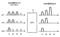
- FIG. 18 is a diagram for explaining the problem. It is assumed that WDM signal light of 3 channels (3 wavelengths) is input to the OPA 5. Also, with respect to the time direction, channel ch1 is 1, 1, 1, 0 intensity modulated light, channel ch2 is 1, 1, 0, 0 intensity modulated light, and channel ch3 is 1, 0, 0. , 0 intensity modulated light.
- the input power is high at time t1, so the amplification factor is low and the output power is low.
- the input power is low and the amplification factor is high and the output power is high.
- a level difference occurs in the output signal light for each time of OPA5.
- the phenomenon of time variation in the amplified output light level is caused by the fact that in OPA5, mutual gain modulation (XGM: CrossCGain Modulation) occurs when the WDM signal light is amplified. It can be seen.
- the mutual gain modulation is a phenomenon in which light of another channel undergoes intensity modulation mutually by turning on / off the light of a certain channel in the input light of a plurality of wavelengths.
- the pumping light moves at high speed in photon energy in units of femtoseconds. At this time, the photon energy of the pumping light is changed to each of the WDM signal light. Since the signal light pulse is not linearly proportionally distributed (linear amplification), time fluctuation occurs in the amplified output light level.
- the EDFA that is generally widely used as an optical amplifier has a response speed in microseconds. For example, even if signal light having a pulse width in picoseconds is input, it follows the time fluctuation of the input light level. Without amplification, it can be amplified at a constant amplification factor.
- the amplification factor is also the same as the time fluctuation of the input light level. It will fluctuate.
- the present invention has been made in view of the above points, and an object thereof is to provide an optical amplifying device that enables amplification while suppressing fluctuations in amplification factor according to the input power of signal light.
- an optical amplifying apparatus that performs optical amplification.
- This optical amplifying device causes each signal light of the wavelength multiplexed signal light to interfere with the optical pulse across multiple codes within the same wavelength, compresses the deviation between the peak power and bottom power of the signal light pulse,
- a multi-symbol interference generator for generating a signal, an optical amplifier having a characteristic of mutual gain modulation, amplifying the interference signal light, and outputting the amplified interference signal light, and canceling the interference of the amplified interference signal light
- a multi-symbol interference canceller that restores the deviation.
- optical amplifier in order to amplify a signal having a small deviation between peak power and bottom power, optical amplification with suppressed mutual gain modulation is performed. Thereafter, the intersymbol interference canceller cancels the interference of the amplified interference signal light and restores the deviation.
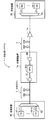
- FIG. 1 is a diagram illustrating a configuration example of an optical amplification device.
- the optical amplifying apparatus 1 includes a multi-symbol interference generator 10, an optical amplifier 20, and a multi-symbol interference canceller 30.
- at least an optical amplifying device according to the following embodiments may be provided in one housing.
- the multi-symbol interference generator 10 causes each signal light waveform included in the received wavelength multiplexed signal light (WDM signal light) to interfere over two or more codes in which one code within the same wavelength is continuous. Then, the deviation (level difference) between the peak power and bottom power of the signal light pulse is compressed to generate interference signal light.
- WDM signal light wavelength multiplexed signal light
- the optical amplifier 20 amplifies the interference signal light and outputs the amplified interference signal light.
- the optical amplifier 20 corresponds to, for example, OPA and is an optical amplifier having a mutual gain modulation characteristic.
- the multi-symbol interference canceler 30 cancels the multi-symbol interference generated by the multi-symbol interference generator 10 with respect to the amplified interference signal light, and calculates the deviation between the peak power and the bottom power of the signal light pulse. Restore.
- Optical parametric amplification applies four-wave mixing (FWM: Four-Wave-Mixing), which is one of nonlinear optical effects generated in an optical fiber.
- FWM is one of the phenomena that should normally be avoided in WDM optical transmission, but depending on the application, it is an important foundation for optical transmission technology.
- G S exp ( ⁇ L) [1 + ⁇ 2 (L)] (1)
- L is the optical fiber length
- ⁇ is the loss factor of the optical fiber.
- ⁇ (L) represents a nonlinear optical phase shift and is given by Expression (2).
- Equation (3) ⁇ ⁇ P P (0) ⁇ k (L) (2)
- P P (0) is the input power of the pumping light
- k (L) is the nonlinear interaction length, which is given by Equation (3).
- ⁇ ( ⁇ ⁇ n 2 ) / (c ⁇ A eff ) (4) Is the optical frequency, n 2 is the nonlinear refractive index in the optical fiber, c is the speed of light, and A eff is the effective core area.
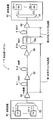
- FIG. 2 is a diagram illustrating the operation of the optical amplification device 1.
- the multi-symbol interference generator 10 is a medium or device that imparts chromatic dispersion, and causes each signal light pulse of the WDM signal light to interfere over multiple codes within the same wavelength, and on the time axis.
- the pulse width is expanded by compressing the deviation between the peak power and the bottom power when combined.
- Interference signal light which is WDM signal light that has undergone intersymbol interference, can greatly suppress the adverse effect of mutual gain modulation that occurs when optical parametric amplification is performed, and can also improve gain linearity.
- the pulse of each signal light is greatly expanded, and interference between multiple codes is performed to compress the deviation between the peak power and the bottom power (ideally, interference is continued until a continuous light (CW) state is reached. is there).
- the effect of leveling out to a low total power can be obtained.
- the pulse width is increased by a factor of 10
- the total power is reduced to about one-tenth, so that the output power of the optical amplifier 20 is not saturated, but is a linear amplification region where the amplification factor does not substantially vary according to the input power. It becomes possible to operate. Even in a saturated region, the adverse effect of the mutual gain modulation can be greatly suppressed because the deviation between the signal lights is compressed.
- the multi-symbol interference canceller 30 is a medium or device that performs chromatic dispersion compensation.
- the amplified interference signal light amplified and output by the optical amplifier 20 is subjected to cancellation of multi-symbol interference by the multi-symbol interference canceller 30, and the deviation between the peak power and the bottom power of the signal light pulse is restored. Is restored (the pulse width of the amplified interference signal light is compressed) and output as amplified signal light.
- the self-phase modulation (SPM (Self-Phase Modulation) that causes the optical spectrum width of the signal light to expand) is a phase modulation that causes the optical spectrum width to expand depending on the peak power of the signal light itself. , Represented by equation (6).
- ⁇ SPM (L) ⁇ ⁇ P S (0) ⁇ k (L) (6)
- P S is the power of the signal light itself.
- cross-phase modulation XPM (Cross-Phase Modulation): phase modulation in which the phase of the signal light fluctuates by turning on / off the signal light of another wavelength
- XPM Cross-phase modulation in which the phase of the signal light fluctuates by turning on / off the signal light of another wavelength
- the following phase modulation is performed by the light power P Sa.
- ⁇ XPM (L) 2 ⁇ ⁇ P Sa (0) ⁇ k (L) (7)
- Both of these phase modulations are proportional to the peak power of the pulse (in the case of nonlinear chirp, it is proportional to the time change of the pulse shape, that is, the slope).
- nonlinear crosstalk is accompanied by the above-described self-phase modulation or cross-phase modulation that causes deterioration of signal quality generated when amplifying signal light of two wavelengths or more.
- FIG. 3 shows the occurrence of nonlinear crosstalk.
- the optical amplifying apparatus 1 reduces or suppresses non-linear crosstalk caused by self-phase modulation or cross-phase modulation in order to reduce the peak power by reducing the optical pulse shape of the signal light and reduce the slope of the pulse. It is also possible to plan.
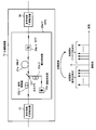
- FIG. 4 is a diagram illustrating a configuration example of an optical amplification device that performs optical amplification by OPA.
- the optical amplifier 20 performs optical parametric amplification, and includes a multi-symbol interference generator 10, an OPA 20a, and a multi-symbol interference canceller 30.
- the OPA 20a includes a highly nonlinear fiber (HNLF) 21a, polarization controllers (PCs) 22a-1 and 22a-2, a pumping light source 23a, an optical coupler C1, and a band pass filter (BPF) 24a.
- the polarization controller 22a-1 corresponds to the first polarization controller
- the polarization controller 22a-2 corresponds to the second polarization controller.
- the HNLF 21a is a highly nonlinear optical fiber with high generation efficiency of nonlinear optical effects.
- a photonic crystal fiber in addition to HNLF, a photonic crystal fiber, a semiconductor optical amplifier, a LiNbO 3 waveguide (PPLN: Periodically Poled Lithium Niobate) having a quasi phase matching structure, a silicon photonics type waveguide, or the like is used. Also good.
- PPLN Periodically Poled Lithium Niobate
- the polarization controller 22a-1 adjusts and controls the polarization (polarization) state of the input signal light.
- the excitation light source 23a emits excitation light. Note that the wavelength of the pumping light is the same as or near to the zero dispersion wavelength of the HNLF 21a (the highest gain can be obtained by making the pumping light having the same wavelength as the zero dispersion wavelength of the HNLF 21a).
- the polarization controller 22a-2 adjusts and controls the polarization state of the excitation light.
- the optical coupler C1 combines the signal light and the excitation light after polarization control, and inputs the combined light to the HNLF 21a.
- the BPF 24a performs filtering to remove the excitation light and idler light generated during optical parametric amplification.
- Each of the polarization controllers 22a-1 and 22a-2 controls the polarization state so that the polarization direction of the signal light and the polarization direction of the excitation light are the same. That is, the polarization state of the signal light and the excitation light is converted so as to be both linearly polarized light, and control is performed so that the polarization states are parallel to each other.
- the signal light is amplified by the FWM, but at the same time, idler light having a new wavelength is also generated. Since the output light from the HNLF 21a includes an idler light component in addition to the signal light and the excitation light, only the signal light component amplified by the BPF 24a is transmitted.
- FIG. 5 is a diagram illustrating a configuration example of an optical amplifying apparatus that performs optical amplification with a polarization diversity configuration.
- the optical amplifier 20 performs polarization diversity amplification, and includes a multi-symbol interference generator 10, a polarization diversity amplifier 20b, and a multi-symbol interference canceller 30.
- the polarization diversity amplifier 20b includes a pumping light source 21b, a polarization controller 22b-1 that adjusts and controls the polarization state of the pumping light, an optical coupler C2 that combines interference signal light and pumping light, and a polarization multiplexing / demultiplexing element. It includes a PBS (Polarization Beam Spliter) 23b, an HNLF 24b, a polarization controller 22b-2, and a BPF 25b.
- the polarization controller 22b-1 corresponds to the first polarization controller
- the polarization controller 22b-2 corresponds to the second polarization controller.
- the PBS 23b has four ports, ports p1 to p4.
- the input end of the polarization controller 22b-2 is connected to the port p2 of the PBS 23b, one end of the HNLF 24b is connected to the output end of the polarization controller 22b-2, and the other end of the HNLF 24b is connected to the port p3 of the PBS 23b.
- a loop R is formed.
- the input end of the BPF 25b is connected to the port p4 of the PBS 23b, and the BPF 25b performs a filtering process on the output light from the loop R (removes the excitation light and idler light and transmits the amplified signal light).
- the OPA 20a in FIG. 4 described above is a polarization-dependent amplifier. Since the excitation light is oscillated from the internal components, fluctuations in the polarization state can be neglected. However, the input signal light propagates through the optical fiber transmission line and reaches the polarization state. Is fluctuating.
- the polarization controller 22a-1 always follows the change in the polarization state of the signal light (the signal light interfered by the multi-symbol interference generator 10) propagating through the optical fiber transmission line.
- the polarization control is performed to match the polarization state of the excitation light (to obtain the maximum efficiency gain by matching the polarization states of the signal light and the excitation light).
- the polarization diversity amplifier 20b in FIG. 5 is a polarization-independent amplifier from which the polarization dependence is removed.
- the amplifier is configured to obtain a gain of maximum efficiency without having a polarization controller for controlling the polarization state of the signal light propagating through the optical fiber transmission line.
- the optical coupler C2 combines the input signal light and the excitation light to output the combined light, and the combined light is input to the port p1 of the PBS 23b.
- the signal light input to the port p1 is polarized and separated into orthogonal components by the PBS 23b, and the optical energy is separated in the x direction at the port p2 and in the y direction at the port p3.
- the optical energy of the signal light separated in the x direction is defined as signal light E Sx
- the optical energy of the signal light separated in the y direction is defined as signal light E Sy .
- the signal light E Sx propagates counterclockwise in the loop R, is amplified by the HNLF 24b, and then enters the port p3. Further, the signal light E Sy propagates clockwise through the loop R, and after being amplified by the HNLF 24b, is input to the port p2.
- the polarization controller 22b-2 rotates the polarization state of the signal light E Sx and E Sy by 90 degrees, thereby causing the signal light E Sx input to the port p3 and the signal light E Sy input to the port p2 to be rotated. Are combined by polarization and output from the port p4.
- the ratio of the optical powers of the signal light E Sx and the signal light E Sy varies depending on the polarization state of the input signal light, but the signal light E Sx and the signal light E Sy are subjected to the same amplification factor in the loop R.
- polarization independent operation is realized. This is achieved by adjusting the excitation light input to the loop R as follows.
- the excitation light is adjusted in polarization state by the polarization controller 22b-1, combined with the signal light by the optical coupler C2, and then input to the port p1 of the PBS 23b.
- the excitation light is polarized and separated by the PBS 23b, and light energy is separated in the x direction at the port p2 and in the y direction at the port p3.
- the light energy of the excitation light separated in the x direction is referred to as excitation light E Px
- the light energy of the excitation light separated in the y direction is referred to as excitation light E Py .
- the optical power ratio between the excitation light E Px and the excitation light E Py can be adjusted by changing the angle input to the PBS 23b by adjusting the polarization controller 22b-1.
- polarization control is performed so that the amplification factors received by the signal lights E Sx and E Sy propagating clockwise and counterclockwise are the same, that is, the optical powers of the excitation lights E Px and E Py are the same.
- the polarization state is adjusted in the unit 22b-1.
- the amplification factors can be set to be equal, and an amplification operation independent of the polarization state of the signal light is enabled.
- the signal light E Sx is amplified by the excitation light E Px and propagates counterclockwise in the loop R
- the signal light E Sy is amplified by the excitation light E Py and rotates in the loop R clockwise.
- the signal light E Sx and the signal light E Sy are amplified with the same amplification factor regardless of the ratio of energy division by the PBS 23b. . Then, by combining and outputting at the port p4 of the PBS 23b, the amplified signal light can be output from the port p4 regardless of the polarization state of the signal light at the port p1.
- FIG. 6 is a diagram illustrating a configuration example of an optical amplifying apparatus that performs optical amplification by SOA.
- the optical amplifying apparatus 1c performs amplification by changing the gain by a drive current to the optical semiconductor, and includes a multi-symbol interference generator 10, an SOA 20c, and a multi-symbol interference canceller 30.
- An optical semiconductor is a medium in which a carrier inversion distribution is formed when a current is applied, and can thereby amplify input light.
- the SOA 20c using such an optical semiconductor can be considered to have a constant inversion distribution and a constant gain value when the input optical power is small, but when the input optical power is large, the inversion distribution decreases due to the stimulated emission process. Along with this, a gain saturation phenomenon occurs in which the gain decreases. When gain saturation occurs, a waveform distortion in which the output signal waveform is not proportional to the input signal waveform occurs, or mutual gain modulation occurs when the WDM signal light is collectively amplified.
- the optical amplifier 20 corresponds to the OPA 20a, the polarization diversity amplifier 20b, the SOA 20c, and the like, which generate mutual gain modulation at the time of optical amplification, and can be applied to any of the optical amplifiers. Then, it demonstrates as what uses OPA20a.
- FIG. 7 is a diagram illustrating a configuration example of an optical amplification device.
- the optical amplifying apparatus 1a-1 includes a multi-symbol interference generator 10-1, an OPA 20a, and an interference canceller 30-1.
- the multi-symbol interference generator 10-1 corresponds to the optical fiber f1
- the multi-symbol interference canceler 30-1 corresponds to the optical fiber f2.
- the optical fiber f1 corresponds to, for example, SMF (Single Mode Fiber) or DCF (Dispersion Compensation Fiber). The same applies to the optical fiber f2, which has chromatic dispersion characteristics (group delay characteristics) opposite to those of the optical fiber f1.
- the WDM signal light When the WDM signal light is input to the optical fiber f1, the WDM signal light propagating through the optical fiber transmission line F1 is subjected to dispersion compensation to some extent at the point P1, and the WDM signal light after dispersion compensation is optical. It is input to the fiber f1 (or there may be a dispersion compensator that performs chromatic dispersion compensation of the WDM signal light that has propagated through the optical fiber transmission line F1 at the point P1).
- FIG. 8 is a diagram illustrating a configuration example of an optical amplification device.
- the optical amplifying device 1a-2 includes a multi-symbol interference generator 10-2, an OPA 20a, and a multi-symbol interference canceller 30-2.
- the multi-symbol interference generator 10-2 includes an optical circulator 11, an FBG 12, and an optical isolator I.
- the multi-symbol interference canceller 30-2 includes an optical circulator 31, an FBG 32, and an optical isolator I.
- An optical isolator is a device that passes required light only in the direction of the arrow in the figure and does not pass light in the reverse direction.
- the port p1 of the optical circulator 11 is connected to one end of the optical fiber transmission line F1 through which the WDM signal light is transmitted, the port p2 is connected to the input / output port p7 of the FBG 12, and the port p3 is connected to the input end (polarization) of the OPA 20a. Connected to the input terminal of the controller 22a-1.
- the port p4 of the optical circulator 31 is connected to the output end of the OPA 20a (the output end of the BPF 24a), the port p5 is connected to the input / output port p8 of the FBG 32, and the port p6 is an optical fiber that outputs WDM signal light. Connected to one end of the transmission line F2.
- the FBG has a grating (diffraction grating) formed on the core of the optical fiber inside the FBG, and the light incident through the optical circulator is reflected by the grating (diffraction grating), and the optical circulator is again used. Output via.
- the grating period changes in the longitudinal direction of the optical fiber, and light of different wavelengths is reflected at different points in the FBG. As a result, a difference in optical path length depending on the wavelength occurs, and the wavelength dispersion characteristic is obtained.
- the WDM signal light that has propagated through the optical fiber transmission line F 1 is input to the port p 1 of the optical circulator 11.
- the WDM signal light input to the port p1 is already subjected to dispersion compensation in the previous stage of the port p1 (a dispersion compensator may exist in the previous stage of the port p1, or the WDM signal light may be present).
- Dispersion compensation may be performed at a relay point or the like on the optical fiber transmission line F1 until the signal light reaches the optical amplifying device 1a-2).
- the optical circulator 11 outputs the received WDM signal light to the port p2.
- the FBG 12 receives the WDM signal light output from the port p2 of the optical circulator 11 at the port p7, and causes the signal light waveform of each channel to interfere over multiple codes. Then, the deviation between the peak power and the bottom power when combined on the time axis is compressed, the pulse width is expanded, and reflected toward the port p 2 of the optical circulator 11.
- the optical circulator 11 When the optical circulator 11 receives the reflected light (interference signal light) from the FBG 12 at the port p2, the optical circulator 11 outputs it from the port p3 and transmits it to the OPA 20a.
- the OPA 20a performs optical parametric amplification of the interference signal light to generate amplified interference signal light, and transmits the amplified interference signal light to the port p4 of the optical circulator 31.
- the optical circulator 31 outputs the received amplified interference signal light to the port p5.
- the FBG 32 receives the amplified interference signal light output from the port p5 of the optical circulator 31 at the port p8, and cancels interference between multiple codes.
- the optical circulator 31 When receiving the reflected light (amplified signal light) from the FBG 32 at the port p5, the optical circulator 31 outputs the light from the port p6 toward the optical fiber transmission line F2.
- FIG. 9 is a diagram showing group delay characteristics of the multi-symbol interference generator 10-2 and the multi-symbol interference canceller 30-2.
- the horizontal axis represents wavelength (nm) and the vertical axis represents group delay (ps).
- the group delay characteristic (group delay function) of the FBG 12 increases the group delay time on the short wavelength side and the group delay time on the long wavelength side with respect to the input WDM signal light ⁇ 1 to ⁇ n, as shown in the graph g11. .
- the FBG 32 having a group delay characteristic whose slope is opposite (reverse sign) from the graph g11. To compensate for chromatic dispersion.
- the group delay time on the short wavelength side is reduced and the group delay time on the long wavelength side is increased with respect to the amplified interference signal light ⁇ 1 to ⁇ n.
- the multi-symbol interference generator 10-2 and the multi-symbol interference canceler 30-2 can perform the same operation as described above if they have group delay characteristics in which the slopes of the group delay functions are opposite to each other. Therefore, the FBG 12 of the multi-symbol interference generator 10-2 has a group delay characteristic as shown in the graph g12, and the FBG 32 of the multi-symbol interference canceller 30-2 as shown in the graph g11. A similar effect can be obtained even with a configuration having delay characteristics.
- FIG. 10 is a diagram showing the reflection characteristics of the multi-symbol interference generator 10-2 and the multi-symbol interference canceller 30-2.
- the horizontal axis represents wavelength (nm), and the vertical axis represents reflected light level (dB).
- the level of the reflected light from the FBG indicates that there is no change for each wavelength.
- the reflected light level after the chromatic dispersion is given by the FBG 12 is equal in the wavelengths ⁇ 1 to ⁇ n of each channel of the WDM signal light. Further, the reflected light level after the chromatic dispersion is compensated by the FBG 32 is the same in the wavelengths ⁇ 1 to ⁇ n of each channel of the WDM signal light.
- FIG. 11 is a diagram illustrating a configuration example of an optical amplification device.
- the optical amplifying apparatus 1a-3 includes a multi-symbol interference generator 10-3, an OPA 20a, and a multi-symbol interference canceler 30-3.
- the multi-symbol interference generator 10-3 includes an optical circulator 11, FBGs # 1- ⁇ 1 to # 1- ⁇ n, and an optical isolator 13.
- Multi-symbol interference canceller 30-3 includes an optical circulator 31, FBGs # 2- ⁇ 1 to # 2- ⁇ n, and an optical isolator 33.
- the input port of the optical isolator 13 is connected to one end of the optical fiber transmission line F1 through which WDM signal light is transmitted, and the output port is connected to the port p1 of the optical circulator 11.
- the port p2 of the optical circulator 11 is connected to the input / output port p7 of FBG # 1- ⁇ 1, and the port p3 is connected to the input terminal of the OPA 20a.
- FBGs # 1- ⁇ 1 to # 1- ⁇ n are serially connected.
- the input port of the optical isolator 33 is connected to the output terminal of the OPA 20a, and the output port is connected to the port p4 of the optical circulator 31.
- the port p5 of the optical circulator 31 is connected to the input / output port p8 of FBG # 2- ⁇ 1, and the port p6 is connected to one end of the optical fiber transmission line F2 that outputs WDM signal light. Further, FBGs # 2- ⁇ 1 to # 2- ⁇ n are serially connected.
- the WDM signal light that has propagated through the optical fiber transmission line F1 passes through the optical isolator 13 and enters the port p1 of the optical circulator 11.
- the WDM signal light input to the port p1 is already subjected to dispersion compensation in the previous stage of the port p1 (a dispersion compensator may exist in the previous stage of the port p1, or the WDM signal light may be present).
- Dispersion compensation may be performed at a relay point or the like on the optical fiber transmission line F1 until the signal light reaches the optical amplifying device 1a-3).
- the optical circulator 11 outputs the received WDM signal light to the port p2.
- Each of FBGs # 1- ⁇ 1 to # 1- ⁇ n receives each channel corresponding to WDM signal light ⁇ 1 to ⁇ n output from the port p2 of the optical circulator 11, and the signal light waveform of each channel is received. Increase the pulse width.
- the pulse width of the signal light having the wavelength ⁇ 1 is enlarged and reflected toward the port p2 of the optical circulator 11.
- the pulse width of the signal light having the wavelength ⁇ 2 is expanded and reflected toward the port p2 of the optical circulator 11.
- the pulse width of the signal light having the wavelength ⁇ n is expanded and reflected toward the port p2 of the optical circulator 11.
- the optical circulator 11 When the optical circulator 11 receives the reflected light (interference signal light) from the FBGs # 1- ⁇ 1 to # 1- ⁇ n at the port p2, the optical circulator 11 outputs it from the port p3 and transmits it to the OPA 20a.
- the OPA 20 a performs optical parametric amplification of the interference signal light to generate amplified interference signal light, and transmits the amplified interference signal light to the optical isolator 33.
- the optical circulator 31 receives the amplified interference signal light that has passed through the optical isolator 33 at the port p4 and outputs it to the port p5.
- Each of the FBGs # 2- ⁇ 1 to # 2- ⁇ n receives each channel corresponding to the amplified interference signal light ⁇ 1 to ⁇ n output from the port p5 of the optical circulator 31, and sets the pulse width of each channel. Compress and restore.
- FBG # 2- ⁇ 1 the pulse width of the signal light having the wavelength ⁇ 1 is restored to the original, and reflected toward the port p5 of the optical circulator 31.
- FBG # 2- ⁇ 2 the pulse width of the signal light having the wavelength ⁇ 2 is restored to the original and reflected toward the port p5 of the optical circulator 31.
- FBG # 2- ⁇ n the pulse width of the signal light having the wavelength ⁇ n is restored and reflected toward the port p5 of the optical circulator 31.
- the optical circulator 31 When the optical circulator 31 receives the reflected light (amplified signal light) from the FBGs # 2- ⁇ 1 to # 2- ⁇ n at the port p5, the optical circulator 31 outputs the light from the port p6 toward the optical fiber transmission line F2.
- the relationship between the group delay characteristics and the reflection characteristics of the multi-symbol interference generator 10-3 and the multi-symbol interference canceler 30-3 of the optical amplifying apparatus 1a-3 are the same as those in FIGS. Omitted.
- FIG. 12 is a diagram illustrating a configuration example of an optical transmission system.
- the optical transmission system 1-1 includes a transmission device 40, a reception device 50, and an optical amplification device 1a.
- the optical amplification device 1a is used as a relay device.
- the transmission device 40 includes transmitters 41-1 to 41-n and a wavelength multiplexer 42, and the reception device 50 includes a wavelength separation unit 51 and reception units 52-1 to 52-n.
- the optical amplifying apparatus 1a includes a multi-symbol interference generator 10, an OPA 20a, and a multi-symbol interference canceller 30, and the multi-symbol interference generator 10 and the multi-symbol interference canceller 30 have the group delay function with respect to each other. It has a group delay characteristic that is reversed.
- the optical fiber transmission line connecting the devices is composed of a DM (Dispersion Managed) line 7.
- the DM line 7 includes SMF and DCF, and is a transmission line that is dispersion managed so that dispersion compensation is performed for each relay section (for example, positive dispersion and negative dispersion are alternately arranged). Thus, a transmission line whose dispersion is approximately compensated).
- Each of the transmitters 41-1 to 41-n in the transmission device 40 outputs signal light having wavelengths ⁇ 1 to ⁇ n.
- the wavelength multiplexer 42 performs wavelength multiplexing of the signal lights ⁇ 1 to ⁇ n to generate WDM signal light.
- WDM signal light propagates through a DM line 7 which is an optical fiber transmission line that compensates for positive and negative chromatic dispersion, and is input to an optical amplifying apparatus 1a used as a repeater.
- the WDM signal light is input to the optical amplifying apparatus 1a on the transmission line of the DM line 7 in a dispersion-compensated state, relayed and amplified by the optical amplifying apparatus 1a, and transmitted to the subsequent stage.
- the wavelength separation unit 51 in the receiving device 50 performs wavelength separation of the propagated WDM signal light and outputs signal light ⁇ 1 to ⁇ n.
- Each of the reception units 52-1 to 52-n performs predetermined reception processing on the signal lights ⁇ 1 to ⁇ n.
- FIG. 13 is a diagram illustrating a modification of the optical transmission system.
- the optical transmission system 1-2 includes a transmission device 40, a reception device 50, a repeater 60, and an OPA 20a.
- the optical fiber transmission line between the transmission device 40 and the reception device 50 includes a first optical fiber transmission line and a second optical fiber transmission line, and the first optical fiber transmission line is formed by a plurality of repeaters 60.
- the SMFs 8-1 to 8-m to be connected are included, and the second optical fiber transmission line is constituted by the DCF 9.
- Each of the transmitters 41-1 to 41-n in the transmission device 40 outputs signal light having wavelengths ⁇ 1 to ⁇ n.
- the wavelength multiplexer 42 performs wavelength multiplexing of the signal lights ⁇ 1 to ⁇ n to generate WDM signal light.
- the WDM signal light output from the transmission device 40 propagates through the SMFs 8-1 to 8-m while being relay-amplified by the repeater 60 arranged at each relay point.
- the SMFs 8-1 to 8-m correspond to the multi-symbol interference generator 10 and are propagated through the SMFs 8-1 to 8-m, thereby causing chromatic dispersion in the WDM signal light, and having chromatic dispersion.
- WDM signal light is input to the OPA 20a in a state where chromatic dispersion (interference) is applied without performing chromatic dispersion compensation.
- the OPA 20a amplifies and outputs the input WDM signal light (corresponding to interference signal light).
- the DCF 9 corresponds to the multi-symbol interference canceller 30 and performs dispersion compensation of the amplified interference signal light output from the OPA 20a to cancel the interference.
- the wavelength separation unit 51 in the receiving device 50 performs wavelength separation of the WDM signal light output from the DCF 9 and outputs signal light ⁇ 1 to ⁇ n.
- Each of the reception units 52-1 to 52-n performs predetermined reception processing on the signal lights ⁇ 1 to ⁇ n.
- the SMFs 8-1 to 8-m are not compensated for the chromatic dispersion on the first optical fiber transmission line. Inter-symbol interference is generated, and the deviation between the peak power and the bottom power of the signal light is compressed.
- the chromatic dispersion is compensated by the DCF 9 to eliminate multi-symbol interference and transmitted to the receiving apparatus 50.
- FIG. 14 is a diagram illustrating a modification of the optical amplifying device 1.
- the optical amplifying device 1d includes a multi-symbol interference generator 10, an OPA 20a-1, and an interference canceller 30.
- the OPA 20a-1 includes an HNLF 21a, polarization controllers 22a-1, 22a-2, a pumping light source 23a, an optical coupler C1, and a BPF 24a-1.
- the substantial configuration of the optical amplifying device 1d is the same as the configuration described above with reference to FIG. 4, and the BPF filtering operation is different.
- multi-code interference is generated by the multi-code interference generator 10 for the WDM signal light of the wavelength group A, and optical parametric amplification is performed by the OPA 20a-1.
- the BPF 24a-1 blocks the excitation light and the amplified WDM signal light of the wavelength group A and transmits the idler light of the wavelength group B.
- the idle light of the wavelength group B is canceled by the multi-symbol interference canceller 30 and returned to the original pulse width and output.
- the OPA not only gives gain to the signal light, but also sends a signal called idler light at a position (frequency band) symmetrical to the original signal light with the wavelength of the excitation light as the center. appear.
- This idler light has the same data as the signal light.
- the OPA can also perform wavelength conversion, and outputs the wavelength-converted amplified signal light by outputting the idler light side component generated during optical amplification by the highly nonlinear fiber as in the optical amplifier 1d. Can also be output.
- the effect of improving the waveform in the optical amplifying apparatus 1 was examined based on the gain characteristics of OPA using HNLF.
- the gain characteristics of the OPA differ depending on the nonlinear coefficient ( ⁇ ) of the HNLF, the fiber (L), and the power (P P ) of the pumping light.
- ⁇ 25 W ⁇ 1 km ⁇ 1
- L 600 m
- P P 27 dBm parameter.
- FIG. 15 is a diagram showing the gain characteristics of OPA.
- the horizontal axis represents the input power (dBm) of the signal light, and the vertical axis represents the gain (dB).
- dBm input power
- dB gain
- FIG. 15 when the power of the input signal light is from ⁇ 20 dBm to around 0 dBm, it is a linear amplification region where a constant gain is obtained (region where an output level with a constant amplification factor is obtained with respect to the input level). When the power increases and exceeds the linear amplification region, a constant gain cannot be obtained.
- the minimum mark level is “1”.
- the maximum value of N is “N” because the mark levels of N wavelengths are all “1” in terms of time.
- FIG. 16 is a diagram showing input / output characteristics of OPA.
- the horizontal axis represents the input level difference (dB), and the vertical axis represents the output level difference (dB).
- dB input level difference
- dB output level difference
- N 40 and 40-wave signal light is input to the OPA.
- Signal light having a level difference of 16 dB may be input to the OPA).
- the level difference of the output signal follows every bit of the ultra high speed signal (> 100 Gb / s) as well as the 2.5 Gb / s and 10 Gb / s signals because the OPA response speed is about femtoseconds.
- the level of the output signal fluctuates at an extremely high speed at the bit level.
- the difference between the OPA output signals can be reduced by compressing the deviation between the bottom level and the mark level by the multi-symbol interference generator 10 of the optical amplifying apparatus 1. is there.
- the multi-symbol interference generator 10 As to how much interference should be generated, from the graph of FIG. 16, for example, if the output level difference is to be suppressed to 0.5 dB ( ⁇ 10%) or less, the multi-symbol interference generator 10 It can be seen that the interference setting may be performed so that the input level difference is about 4.5 dB or less at the 1 dB saturation point, and about 1.5 dB or less at the 2 dB saturation point, and about 1 dB or less at the 3 dB saturation point. .
- Gain characteristics differ depending on the nonlinear coefficient of HNLF, fiber length, pumping light power, and signal format. Accordingly, the input / output characteristics corresponding to FIG. 16 are obtained according to these, and the requirements required for the multi-symbol interference generator 10 are determined.
- the optical signal amplification apparatus 1 when the optical amplification apparatus 1 performs optical amplification with an optical amplifier having the characteristics of mutual gain modulation in the amplification of WDM signal light, the optical signal amplification apparatus 1 causes each signal light waveform included in the WDM signal light to interfere, Optical amplification is performed after compressing the deviation between the peak power and bottom power of the signal light waveform, and after optical amplification, the deviation between the peak power and bottom power of the signal light waveform is restored by eliminating interference. .
Landscapes
- Engineering & Computer Science (AREA)
- Computer Networks & Wireless Communication (AREA)
- Signal Processing (AREA)
- Optical Communication System (AREA)
- Optical Modulation, Optical Deflection, Nonlinear Optics, Optical Demodulation, Optical Logic Elements (AREA)
Abstract
信号光の入力パワーの瞬間変動に対して利得の線形性を向上する。 多符号間干渉発生器は、受信した波長多重信号光に含まれる各信号光パルスを、同一の波長内において多符号間に渡って干渉させて、信号光パルスのピークパワーとボトムパワーとの偏差を圧縮して、干渉信号光を生成する。光増幅器は、相互利得変調の特性を有し、偏差の圧縮された干渉信号光を増幅して、増幅干渉信号光を出力する。多符号間干渉解消器は、干渉を解消して信号光パルスのピークパワーとボトムパワーとの偏差を復元する。
Description
本発明は、信号光の光増幅を行う光増幅装置に関する。
光通信ネットワークを構築するキーデバイスである光増幅器には、エルビウム添加光ファイバ増幅器(EDFA:Erbium Doped Fiber Amplifier)、半導体光増幅器(SOA:Semiconductor Optical Amplifier)、ラマンアンプ(Raman Amplifier)等があり広く実用化されている。
一方、近年では、これらの光増幅器に比べ、雑音指数の低い低雑音光増幅器である光パラメトリック増幅器(OPA:Optical Parametric Amplifier)が注目されている。
OPAは、非線形光学効果(ガラス中に比較的強いパワーの光を伝搬させたときに、光強度に応じてガラスの物性が変化して、光学的な応答が線形性を失う現象)の発生効率が高い高非線形ファイバ(HNLF:High Non-Linear Fiber)に対し、信号光と励起光を入力して、パラメトリック増幅(Parametric Amplification)を起こさせる。
OPAは、非線形光学効果(ガラス中に比較的強いパワーの光を伝搬させたときに、光強度に応じてガラスの物性が変化して、光学的な応答が線形性を失う現象)の発生効率が高い高非線形ファイバ(HNLF:High Non-Linear Fiber)に対し、信号光と励起光を入力して、パラメトリック増幅(Parametric Amplification)を起こさせる。
パラメトリック増幅は、非線形光学効果によって信号光の強度を増幅するものであり、従来のEDF(Erbium-Doped Fiber)のような線形増幅媒体を用いずに、信号光と励起光とが高非線形ファイバの中で相互作用することで生じる現象である。
OPAは、従来の光増幅器よりも低雑音であり、広帯域、超高速(フェムト秒単位)に動作する特徴を持つ。また、帯域については、EDFAの増幅帯域外においても動作させることが可能である。
従来技術としては、励起光の波長を含む増幅帯域を有して励起光を増幅して出力する第1光増幅器と、第1光増幅器から出力される励起光を第1光増幅器の増幅帯域外に波長を有する信号光とともに非線形光学媒質に供給する光パラメトリック増幅器が提案されている(特許文献1)。また、WDM(Wavelength Division Multiplexing)信号光の光パラメトリック増幅を行う光パラメトリック増幅器が提案されている(非特許文献1)。
Amplification of WDM Signals in Fiber-Based Optical Parametric Amplifiers, Tomas Torounidis et. al., IEEE PHOTONICS TECHNOLOGY LETTERS, VOL. 15 NO.8, 2003, pp1061-1063
OPAでは、入力する信号光のパワーが増大して、励起光のパワーに近づいていくと、励起光のエネルギーが枯渇して増幅率が低下し、出力パワーが飽和する現象が発生する。
図17はOPAの入出力特性を示す図である。横軸はOPAへの信号光の入力パワー、縦軸はOPAによって増幅された後の信号光の出力パワーである。
図17はOPAの入出力特性を示す図である。横軸はOPAへの信号光の入力パワー、縦軸はOPAによって増幅された後の信号光の出力パワーである。
光パラメトリック増幅時、励起光のエネルギーが入力信号光に与えられて、信号光は増幅されて出力するが(実際にはアイドラ(idler)光も発生する)、信号光パワーが励起光パワーと同一レベルに近づくにつれて、図17に示すように、信号光の増幅率が低下して出力パワーが飽和する。
このような特性を持つOPAに対して、波長多重された多波長信号(WDM信号)光を入力して増幅を起こさせるとする。この場合、WDM信号光では、信号間のデータタイミングによって、OPAへ入力するときの入力パワーが時間的に変動するが、OPAは、超高速(フェムト秒単位)に応答し、入力パワーによって利得が異なるため、利得が時間的に異なる現象(利得変調)が発生してしまう。このため、WDM信号光を増幅する場合、一定の増幅率で増幅することができないといった問題があった。
図18は問題点を説明するための図である。3チャネル(3波長)のWDM信号光がOPA5に入力するものとする。また、時間方向に対して、チャネルch1は1、1、1、0の強度変調光であり、チャネルch2は1、1、0、0の強度変調光であり、チャネルch3は1、0、0、0の強度変調光であるとする。
時間t1におけるWDM信号光の入力パワーは3(=1+1+1)となり、時間t2では、WDM信号光の入力パワーは2(=1+1+0)となり、時間t3では、WDM信号光の入力パワーは1(=1+0+0)となる。
このように、入力パワーに時間変動を持つWDM信号光が、OPA5に入力すると、時間t1~t3のそれぞれの入力パワーが異なるので、時間t1~t3の入力光に対する増幅率も異なり、OPA5の増幅出力光レベルには時間変動が生じることになる。
この例の場合、時間t1では入力パワーが高いので、増幅率が低くなって出力パワーが低くなるが、時間t3では入力パワーが低いために増幅率が高くなって出力パワーが高くなる。結果的にOPA5の時間毎の出力信号光にレベル差が生じてしまう。
上記のように、増幅出力光レベルに時間変動が生じる現象は、OPA5においては、WDM信号光の増幅の際には、相互利得変調(XGM:Cross Gain Modulation)が発生していることが原因と見られる。相互利得変調は、入力された複数の波長の光において、あるチャネルの光のオン/オフにより、他のチャネルの光が相互に強度変調を受ける現象である。
OPA5において、WDM信号光と励起光との間で相互利得変調が生じると、励起光がフェムト秒単位でフォトンエネルギーの高速移動が行われ、このとき、励起光のフォトンエネルギーがWDM信号光の各信号光パルスに線形的に比例分配(線形増幅)されないために、増幅出力光レベルに時間変動が生じてしまう。
これは、時間軸上においてWDM信号光のエネルギー分布の偏差が極めて大きいことに起因するものである(なお、WDM信号光を一定の増幅率で増幅できない現象については、上記の非特許文献1にも指摘されている)。
光増幅器として一般的に広く用いられるEDFAでは、マイクロ秒単位の応答速度であるので、例えば、ピコ秒単位のパルス幅を持つ信号光が入力しても、その入力光レベルの時間変動には追従せず、一定の増幅率で増幅することができる。
しかし、従来のOPA5の場合は、フェムト秒単位で応答する高速性を持つために、ピコ秒単位のパルス幅を持つ信号光が入力すると、その入力光レベルの時間変動と同じように増幅率も変動してしまうのである。
なお、上記ではOPAに関する問題点として説明したが、上記の問題点は、OPAに限るものではなく、相互利得変調特性を有する光増幅器として、例えば、SOA等についても同様に生じるものである。
本発明はこのような点に鑑みてなされたものであり、信号光の入力パワーに応じた増幅率の変動を抑制した増幅を可能にした光増幅装置を提供することを目的とする。
上記課題を解決するために、光増幅を行う光増幅装置が提供される。この光増幅装置は、波長多重信号光の各信号光を、同一波長内において多符号間に渡り光パルスを干渉させ、信号光パルスのピークパワーとボトムパワーとの偏差を圧縮し、干渉信号光を生成する多符号間干渉発生器と、相互利得変調の特性を有し、前記干渉信号光を増幅して、増幅干渉信号光を出力する光増幅器と、前記増幅干渉信号光の干渉を解消して、前記偏差を復元する多符号間干渉解消器とを有する。
光増幅器では、ピークパワーとボトムパワーの偏差が小さい信号を増幅するために、相互利得変調が抑制された光増幅が行われる。その後、多符号間干渉解消器は、増幅された干渉信号光の干渉を解消して偏差を復元する。
信号光の入力パワーの瞬間変動に応じた増幅率の変動を抑制して、利得の線形性を向上することが可能になる。
本発明の上記および他の目的、特徴および利点は本発明の例として好ましい実施の形態を表す添付の図面と関連した以下の説明により明らかになるであろう。
本発明の上記および他の目的、特徴および利点は本発明の例として好ましい実施の形態を表す添付の図面と関連した以下の説明により明らかになるであろう。
以下、本発明の実施の形態を図面を参照して説明する。図1は光増幅装置の構成例を示す図である。光増幅装置1は、多符号間干渉発生器10、光増幅器20および多符号間干渉解消器30を備える。別の態様では、1つの筐体の中に少なくとも以下の実施例にかかる光増幅装置を備えてもよい。
多符号間干渉発生器10は、受信した波長多重信号光(WDM信号光)に含まれる各信号光波形を、同一の波長内の1つの符号が連続した2つ以上の符号に渡って干渉させて、信号光パルスのピークパワーとボトムパワーとの偏差(レベル差)を圧縮して、干渉信号光を生成する。
光増幅器20は、干渉信号光を増幅して、増幅干渉信号光を出力する。光増幅器20は、例えば、OPAに該当し、相互利得変調の特性を有する光増幅器である。多符号間干渉解消器30は、増幅干渉信号光に対して、多符号間干渉発生器10で発生させた多符号間干渉を解消して、信号光パルスのピークパワーとボトムパワーとの偏差を復元する。
次に光パラメトリック増幅の動作について説明する。光パラメトリック増幅は、光ファイバ中で発生する非線形光学効果の1つである四光波混合(FWM:Four Wave Mixing)を応用している。FWMは、WDMの光伝送において通常は回避すべき現象の1つであるが、応用によっては光伝送技術の重要な基盤となるものである。
FWMは、光ファイバの零分散波長(λ0)に、同じ波長の励起光(λP)と、励起光とは異なる波長の信号光(λS)を光ファイバに入射すると、第三の光であるアイドラ光(λI)が発生する現象である。
以下、1波の信号光における光パラメトリック増幅について説明する。信号光と励起光との間の相互作用において、励起光のエネルギーの一部が、信号光およびアイドラ光にほぼ均等に与えられる。FWMを用いたOPAでは、入力される信号光のパワーが、励起光のパワーに比べて十分に小さい場合、OPAの増幅率は励起光のパワーと高非線形ファイバの特性によって決まり、ほぼ一定の値をとる。
光ファイバから出力される信号光の利得GSは、式(1)のように記述される。
GS=exp(-αL)[1+φ2(L)]・・・(1)
なお、Lは光ファイバ長、αは光ファイバの損失係数である。また、φ(L)は、非線形光位相シフトを表し、式(2)で与えられる。
GS=exp(-αL)[1+φ2(L)]・・・(1)
なお、Lは光ファイバ長、αは光ファイバの損失係数である。また、φ(L)は、非線形光位相シフトを表し、式(2)で与えられる。
φ(L)=γ・PP(0)・k(L)・・・(2)
ここで、PP(0)は、励起光の入力パワーであり、k(L)は非線形相互作用長であって、式(3)で与えられる。
ここで、PP(0)は、励起光の入力パワーであり、k(L)は非線形相互作用長であって、式(3)で与えられる。
k(L)=(1-exp(-αL))/αL・・・(3)
また、γは、三次非線形定数を表し、式(4)で与えられる。
γ=(ω・n2)/(c・Aeff)・・・(4)
なお、ωは光周波数、n2は光ファイバ内の非線形屈折率、cは光速、Aeffは有効コア断面積を表す。
また、γは、三次非線形定数を表し、式(4)で与えられる。
γ=(ω・n2)/(c・Aeff)・・・(4)
なお、ωは光周波数、n2は光ファイバ内の非線形屈折率、cは光速、Aeffは有効コア断面積を表す。
ここで、信号光の周波数をωS、励起光の周波数をωP、アイドラ光の周波数をωCとすると、下記の式(5)の関係を満足する。
ωP-ωC=ωS-ωP≠0・・・(5)
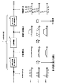
次に光増幅装置1の動作について説明する。図2は光増幅装置1の動作を示す図である。多符号間干渉発生器10は、波長分散量を付与する媒質または装置であって、WDM信号光の各信号光パルスを、同一の波長内において多符号に渡って干渉させて、時間軸上で合成したときのピークパワーとボトムパワーとの偏差を圧縮してパルス幅を拡大させる。
ωP-ωC=ωS-ωP≠0・・・(5)
次に光増幅装置1の動作について説明する。図2は光増幅装置1の動作を示す図である。多符号間干渉発生器10は、波長分散量を付与する媒質または装置であって、WDM信号光の各信号光パルスを、同一の波長内において多符号に渡って干渉させて、時間軸上で合成したときのピークパワーとボトムパワーとの偏差を圧縮してパルス幅を拡大させる。
多符号間干渉したWDM信号光である干渉信号光は、光パラメトリック増幅したときに生じる相互利得変調の悪影響を大きく抑制することができるとともに、利得の線形性を向上することができる。
例えば、時間的にデータ信号(マークレベル)が多いタイミング(時間t1)の場合には、そのまま高い合計パワーで光増幅すると、出力パワーが飽和してしまうが、これを多符号間干渉発生器10によって、各信号光のパルスを大幅に拡大し、多符号間で干渉させてピークパワーとボトムパワーの偏差を圧縮させる(連続光(CW:continuous wave)状態になるまで干渉させるのが理想的である)。
多符号間干渉を生じさせることによって、低い合計パワーに均される効果が得られる。パルス幅が10倍になれば、およそ10分の1程度の合計パワーに下がるため、光増幅器20の出力パワーが飽和した領域ではなく、入力パワーに応じて増幅率がほぼ変動しない線形増幅領域で動作させることが可能になる。また、飽和した領域であっても、信号光間の偏差が圧縮されているため、相互利得変調の悪影響を大きく抑圧することができる。
一方、多符号間干渉解消器30は、波長分散補償を行う媒質または装置である。光増幅器20で増幅出力された増幅干渉信号光は、多符号間干渉解消器30によって、多符号間干渉が解消され、信号光パルスのピークパワーとボトムパワーとの偏差が復元されて、パルス幅が元に戻され(増幅干渉信号光のパルス幅が圧縮され)、増幅信号光となって出力する。このような処理を施すことによって、光増幅器20の相互利得変調の悪影響を抑圧・低減した多波長の一括線形増幅が可能になる。
ここで、信号光の光スペクトル幅の拡大を引き起こす自己位相変調(SPM(Self-Phase Modulation):信号光自身のピークパワーに応じて発生量が変わり、光スペクトル幅の拡大を引き起こす位相変調)は、式(6)により表される。
φSPM(L)=γ・PS(0)・k(L)・・・(6)
PSは、信号光自身のパワーである。また、相互位相変調(XPM(Cross-Phase Modulation):他波長の信号光のオン/オフにより信号光の位相が変動する位相変調)は、変調を受ける信号光とは異なる波長を持つ別の信号光のパワーPSaによって、下記の位相変調を受ける。
PSは、信号光自身のパワーである。また、相互位相変調(XPM(Cross-Phase Modulation):他波長の信号光のオン/オフにより信号光の位相が変動する位相変調)は、変調を受ける信号光とは異なる波長を持つ別の信号光のパワーPSaによって、下記の位相変調を受ける。
φXPM(L)=2γ・PSa(0)・k(L)・・・(7)
これらの位相変調は、ともにパルスのピークパワーに比例する(非線形チャープとする場合には、パルス形状の時間変化、つまり傾きに比例する)。
これらの位相変調は、ともにパルスのピークパワーに比例する(非線形チャープとする場合には、パルス形状の時間変化、つまり傾きに比例する)。
ここで、従来の光増幅において、例えばOPAでは、上記の自己位相変調や、2波長以上の信号光を増幅する際に発生する信号品質の劣化を招く相互位相変調等により、非線形クロストークが伴うといった問題があった。なお、図3に非線形クロストークの発生の様子を示す。従来のOPA5において光パラメトリック増幅を行うと、増幅された信号光の近傍波長に対して、非線形クロストークが発生する。
これに対し、光増幅装置1では、信号光の光パルス形状を広げることでピークパワーを下げ、パルスの傾きを小さくするため、自己位相変調や相互位相変調等で生じる非線形クロストークの低減、抑圧を図ることも可能になる。
次に光増幅装置1の構成について詳しく説明する。最初に光パラメトリック増幅器を適用した光増幅装置について説明する。
図4はOPAによって光増幅を行う光増幅装置の構成例を示す図である。光増幅装置1aは、光増幅器20が光パラメトリック増幅を行うものであり、多符号間干渉発生器10、OPA20aおよび多符号間干渉解消器30を備える。
図4はOPAによって光増幅を行う光増幅装置の構成例を示す図である。光増幅装置1aは、光増幅器20が光パラメトリック増幅を行うものであり、多符号間干渉発生器10、OPA20aおよび多符号間干渉解消器30を備える。
OPA20aは、高非線形ファイバ(HNLF)21a、偏光制御器(PC:Polarization Controller)22a-1、22a-2、励起光光源23a、光カプラC1およびバンドパスフィルタ(BPF:Band Pass Filter)24aを含む。なお、偏光制御器22a-1は、第1の偏光制御器に該当し、偏光制御器22a-2は、第2の偏光制御器に該当する。
HNLF21aは、非線形光学効果の発生効率が高い高非線形光ファイバである。なお、非線形媒質としては、HNLFの他に、フォトニック結晶ファイバ、半導体光アンプ、擬似位相整合構造を有するLiNbO3導波路(PPLN:Periodically Poled Lithium Niobate)、シリコンフォトニクス型導波路等を使用してもよい。
偏光制御器22a-1は、入力信号光の偏光(偏波)状態を調整・制御する。励起光光源23aは、励起光を発出する。なお、励起光の波長は、HNLF21aの零分散波長に対して同一または近傍の波長とする(HNLF21aの零分散波長と同じ波長の励起光を入射することで最も高い利得を得ることができる)。
偏光制御器22a-2は、励起光の偏光状態を調整・制御する。光カプラC1は、偏光制御された後の信号光および励起光を合波して、合波光をHNLF21aに入力する。BPF24aは、励起光と、光パラメトリック増幅時に発生するアイドラ光とを除去するフィルタリングを行う。
動作について説明する。偏光制御器22a-1、22a-2それぞれは、信号光の偏光方向と励起光の偏光方向とが同一となるように偏光状態を制御する。すなわち、信号光と励起光の偏光状態がともに直線偏光となるように変換し、互いに平行な偏光状態となるように制御する。
偏光状態がともに直線偏光で互いに平行な偏光状態である信号光と励起光とが、光カプラC1で合波されてHNLF21aに入力することにより、HNLF21a内で光パラメトリック増幅が最大効率で生じて最大の利得が発生することになる(なお、信号光と励起光との偏光状態が直交する場合には、HNLF21a内では殆どFWMは発生しないので、光パラメトリック増幅が生じない)。
なお、HNLF21aの内部では、FWMによって信号光が増幅されるが、同時に新たな波長のアイドラ光も発生する。HNLF21aからの出力光には、信号光と励起光の他にアイドラ光の成分があるために、BPF24aによって、増幅された信号光成分のみを透過させる。
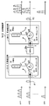
次に偏波ダイバーシティ構成を適用した光増幅装置について説明する。図5は偏波ダイバーシティ構成によって光増幅を行う光増幅装置の構成例を示す図である。光増幅装置1bは、光増幅器20が偏波ダイバーシティ増幅を行うものであり、多符号間干渉発生器10、偏波ダイバーシティ増幅器20bおよび多符号間干渉解消器30を備える。
偏波ダイバーシティ増幅器20bは、励起光光源21b、励起光の偏光状態を調整・制御する偏光制御器22b-1、干渉信号光と励起光を合波する光カプラC2、偏波合分波素子であるPBS(Polarization Beam Splitter:偏光ビームスプリッタ)23b、HNLF24b、偏光制御器22b-2およびBPF25bを含む。なお、偏光制御器22b-1は、第1の偏光制御器に該当し、偏光制御器22b-2は、第2の偏光制御器に該当する。
PBS23bは、ポートp1~p4の4つのポートを有している。PBS23bのポートp2に、偏光制御器22b-2の入力端が接続し、偏光制御器22b-2の出力端にHNLF24bの一端が接続し、HNLF24bの他端がPBS23bのポートp3に接続することで、ループRが形成される。
また、BPF25bの入力端は、PBS23bのポートp4に接続し、BPF25bは、ループRからの出力光に対するフィルタリング処理を行う(励起光とアイドラ光を除去して増幅信号光を透過させる)。
ここで、上述した図4のOPA20aは、偏光依存型の増幅器である。励起光は内部の構成要素から発振されるものであるから、偏光状態の変動はほとんど無視することができるが、入力信号光は、光ファイバ伝送路等を伝搬して到達することにより、偏光状態が変動している。
したがって、OPA20aの構成においては、偏光制御器22a-1によって、光ファイバ伝送路を伝搬してきた信号光(多符号間干渉発生器10によって干渉されている信号光)の偏光状態の変動を常に追随しながら偏光制御を行って、励起光の偏光状態と一致させている(信号光と励起光との偏光状態を一致させて最大効率の利得を得るため)。
これに対し、図5の偏波ダイバーシティ増幅器20bでは、偏光依存性を除去した偏光無依存型の増幅器である。光ファイバ伝送路を伝搬してきた信号光の偏光状態を制御する偏光制御器を持たずに、最大効率の利得を得るように構成された増幅器である。
動作について説明する。光カプラC2は、入力信号光と励起光とを合波して、合波光を出力し、合波光は、PBS23bのポートp1へ入力する。ポートp1へ入力した信号光は、PBS23bによって直交成分が偏光分離され、ポートp2においてはx方向、ポートp3においてはy方向にそれぞれ光エネルギーが分離される。x方向に分離された信号光の光エネルギーを信号光ESx、y方向に分離された信号光の光エネルギーを信号光ESyとする。
信号光ESxは、ループRを反時計回りに伝搬し、HNLF24bで増幅を受けた後、ポートp3へ入力する。また、信号光ESyは、ループRを時計回りに伝搬し、HNLF24bで増幅を受けた後、ポートp2へ入力する。
このとき、偏光制御器22b-2によって、信号光ESx、ESyの偏光状態を90度回転させることによって、ポートp3に入力された信号光ESxとポートp2に入力された信号光ESyは、偏光合成されてポートp4から出力される。
信号光ESxと信号光ESyの光パワーの比は、入力される信号光の偏光状態によって変動するが、信号光ESxと信号光ESyがループR内部で受ける増幅率が同じであれば、偏光無依存動作が実現される。これは、ループRに入力される励起光を以下のように調整することで達成される。
励起光は、偏光制御器22b-1によって偏光状態が調整され、光カプラC2により信号光と合波された後に、PBS23bのポートp1へ入力される。励起光は、PBS23bにより偏光分離され、ポートp2においてはx方向、ポートp3においてはy方向にそれぞれ光エネルギーが分離される。x方向に分離された励起光の光エネルギーを励起光EPx、y方向に分離された励起光の光エネルギーを励起光EPyとする。
励起光EPxと励起光EPyの光パワー比は、偏光制御器22b-1を調整することによって、PBS23bへ入力する角度を変えて調整することができる。このとき、時計回りと反時計回りに伝搬する信号光ESx、ESyが受ける増幅率が同じになるように、すなわち励起光EPx、EPyの光パワーが同じになるように、偏光制御器22b-1において偏光状態を調整する。これによって、増幅率を等しく設定することができ、信号光の偏光状態に依存しない増幅動作を可能にする。
上記の動作についてまとめると、PBS23bのポートp1へ励起光を入力した場合、ポートp2から励起光EPxが出力し、ポートp3から励起光EPyが出力する。励起光EPxと励起光EPyとは互いに等しい光エネルギーである。そして、このような励起光が設定入力されているときに、信号光がPBS23bに入力し、ポートp2から信号光ESxが出力し、ポートp3から信号光ESyが出力する。
すると、HNLF24b内において、信号光ESxは、励起光EPxによって増幅されてループRを反時計周りに伝搬し、信号光ESyは、励起光EPyによって増幅されてループRを時計周りに伝搬する。
励起光EPxと励起光EPyとは共に同じ励起パワーであるので、信号光ESxと信号光ESyとは、PBS23bによってエネルギーが分割される比率にかかわらず、同じ増幅率で増幅される。そして、PBS23bのポートp4において合成出力することにより、ポートp1における信号光の偏光状態によらずに、ポートp4から増幅された信号光が出力できるのである。
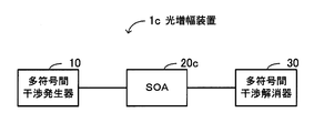
次にSOAを適用した光増幅装置について説明する。図6はSOAによって光増幅を行う光増幅装置の構成例を示す図である。光増幅装置1cは、光半導体への駆動電流により利得を変化させて増幅を行うものであり、多符号間干渉発生器10、SOA20cおよび多符号間干渉解消器30を備える。
光半導体は、電流を印加するとキャリアの反転分布が形成される媒質であり、これにより入力光に対して増幅作用を及ぼすことができる。このような光半導体を用いたSOA20cは、入力光パワーが小さいときには反転分布は一定で利得値を一定とみなすことができるが、入力光パワーが大きいと、誘導放出過程により反転分布が減少し、これに伴い利得が低下する利得飽和現象が発生する。利得飽和が起こると、出力信号波形が入力信号波形に比例しない波形歪を生じたり、WDM信号光を一括増幅する際には、相互利得変調が生じたりすることになる。
したがって、このような特性を持つSOA20cを使用して光増幅する場合にも、光増幅装置1の機能・構成を備えることにより(すなわち、多符号間干渉発生器10および多符号間干渉解消器30を備えることにより)、WDM信号光の入力パワーに応じた増幅率の変動を抑制して、線形増幅を行うことが可能になる。
次に光増幅装置1の多符号間干渉発生器10および多符号間干渉解消器30の具体的な構成について説明する。なお、光増幅器20としては、光増幅時に相互利得変調が生じる、上記のようなOPA20a、偏波ダイバーシティ増幅器20b、SOA20c等が該当し、いずれの光増幅器に対しても対応可能なので、以降の説明では、OPA20aを使用するものとして説明する。
図7は光増幅装置の構成例を示す図である。光増幅装置1a-1は、多符号間干渉発生器10-1、OPA20aおよび干渉解消器30-1を備える。多符号間干渉発生器10-1は、光ファイバf1に該当し、多符号間干渉解消器30-1は、光ファイバf2に該当する。
光ファイバf1は、例えば、SMF(Single Mode Fiber)、DCF(Dispersion Compensation Fiber)が該当する。光ファイバf2も同様であり、光ファイバf1と反対符号の波長分散特性(群遅延特性)を有するものである。
なお、WDM信号光が光ファイバf1に入力する際には、光ファイバ伝送路F1を伝搬してきたWDM信号光は、ポイントP1において分散補償がある程度なされており、分散補償後のWDM信号光が光ファイバf1に入力するものである(または、ポイントP1において、光ファイバ伝送路F1を伝搬してきたWDM信号光の波長分散補償を実行する分散補償器が存在してもよい)。
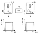
次に多符号間干渉発生器10および多符号間干渉解消器30がFBG(Fiber Bragg Grating:ファイバ・ブラッグ・グレーティング)を含む場合の光増幅装置について説明する。図8は光増幅装置の構成例を示す図である。光増幅装置1a-2は、多符号間干渉発生器10-2、OPA20aおよび多符号間干渉解消器30-2を備える。多符号間干渉発生器10-2は、光サーキュレータ11とFBG12、光アイソレータIを含む。多符号間干渉解消器30-2は、光サーキュレータ31とFBG32、光アイソレータIを含む。なお、光アイソレータは、図の矢印方向にのみ所要の光を通して、逆方向には光は通さないデバイスである。
光サーキュレータ11のポートp1は、WDM信号光が伝送される光ファイバ伝送路F1の一端と接続し、ポートp2は、FBG12の入出力ポートp7と接続し、ポートp3は、OPA20aの入力端(偏光制御器22a-1の入力端)と接続する。
一方、光サーキュレータ31のポートp4は、OPA20aの出力端(BPF24aの出力端)と接続し、ポートp5は、FBG32の入出力ポートp8と接続し、ポートp6は、WDM信号光を出力する光ファイバ伝送路F2の一端と接続する。
なお、FBGは、FBG内部の光ファイバのコア上にグレーティング(回折格子)が形成されており、光サーキュレータを介して入射された光を、グレーティング(回折格子)で反射して、再び光サーキュレータを介して出力する。FBGでは、グレーティングの周期が光ファイバの長手方向に変化しており、異なる波長の光は、FBG内の異なる点で反射する。これにより、波長による光路長差が生じて波長分散特性を有することになる。
ここで、光ファイバ伝送路F1を伝搬してきたWDM信号光は、光サーキュレータ11のポートp1に入力する。なお、ポートp1に入力するときのWDM信号光は、ポートp1の前段においてすでに分散補償が施されているものである(ポートp1の前段部に分散補償器が存在していてもよいし、WDM信号光が光増幅装置1a-2に到達するまでに、光ファイバ伝送路F1上の中継ポイント等で分散補償が施されていてもよい)。
光サーキュレータ11は、受信したWDM信号光をポートp2へ出力する。FBG12は、光サーキュレータ11のポートp2から出力されたWDM信号光をポートp7で受信し、各チャネルの信号光波形を多符号に渡って干渉させる。そして、時間軸上で合成したときのピークパワーとボトムパワーとの偏差を圧縮してパルス幅を拡大させ、光サーキュレータ11のポートp2へ向けて反射させる。
光サーキュレータ11は、FBG12からの反射光(干渉信号光)をポートp2で受信すると、ポートp3から出力してOPA20aへ送信する。OPA20aは、干渉信号光の光パラメトリック増幅を行って増幅干渉信号光を生成し、光サーキュレータ31のポートp4へ向けて送信する。
光サーキュレータ31は、受信した増幅干渉信号光をポートp5へ出力する。FBG32は、光サーキュレータ31のポートp5から出力された増幅干渉信号光をポートp8で受信し、多符号間の干渉を解消する。
そして、信号光波形のピークパワーとボトムパワーとの偏差を復元して、パルス幅を元に戻し、光サーキュレータ31のポートp5へ向けて反射させる。光サーキュレータ31は、FBG32からの反射光(増幅信号光)をポートp5で受信すると、ポートp6から光ファイバ伝送路F2へ向けて出力する。
図9は多符号間干渉発生器10-2および多符号間干渉解消器30-2の群遅延特性を示す図である。横軸は波長(nm)、縦軸は群遅延(ps)である。FBG12の群遅延特性(群遅延関数)は、グラフg11に示すように、入力WDM信号光λ1~λnに対し、短波長側の群遅延時間を大きくし、長波長側の群遅延時間を小さくする。
これによって、各チャネルの信号光パルスに対して波長分散を与えて、多符号間に渡って干渉させ、時間軸上で合成したときのピークパワーとボトムパワーとの偏差を圧縮して、パルス幅を拡大させる。
一方、OPA20aによる光パラメトリック増幅後のパルス幅が拡大している増幅干渉信号光を、元のパルス幅に戻すためには、グラフg11とは傾きが逆(逆符号)の群遅延特性を持つFBG32によって波長分散補償を施す。
すなわち、FBG32の群遅延特性は、グラフg12に示すように、増幅干渉信号光λ1~λnに対し、短波長側の群遅延時間を小さくし、長波長側の群遅延時間を大きくする。これによって、各チャネルの信号光波形に対して波長分散を補償して、多符号間の干渉を解消し、信号光波形のピークパワーとボトムパワーとの偏差を復元して、パルス幅を元に戻す。
なお、多符号間干渉発生器10-2および多符号間干渉解消器30-2では、互いに群遅延関数の傾きが逆方向となる群遅延特性を持たせれば上記と同じ動作が行える。したがって、多符号間干渉発生器10-2のFBG12に対して、グラフg12のような群遅延特性を持たせ、多符号間干渉解消器30-2のFBG32に対して、グラフg11のような群遅延特性を持たせるような構成にしても同様な効果が得られる。
図10は多符号間干渉発生器10-2および多符号間干渉解消器30-2の反射特性を示す図である。横軸は波長(nm)、縦軸は反射光のレベル(dB)である。FBGからの反射光のレベルは、波長毎に変化はないことを示している。
すなわち、FBG12によって波長分散が付与された後の反射光レベルは、WDM信号光の各チャネルの波長λ1~λnにおいて等しい。また、FBG32によって波長分散が補償された後の反射光レベルは、WDM信号光の各チャネルの波長λ1~λnにおいて等しい。
次に多段接続されたFBGを含む多符号間干渉発生器10および多符号間干渉解消器30を有する光増幅装置について説明する。図11は光増幅装置の構成例を示す図である。光増幅装置1a-3は、多符号間干渉発生器10-3、OPA20aおよび多符号間干渉解消器30-3を備える。
多符号間干渉発生器10-3は、光サーキュレータ11、FBG#1-λ1~#1-λnおよび光アイソレータ13を含む。多符号間干渉解消器30-3は、光サーキュレータ31、FBG#2-λ1~#2-λnおよび光アイソレータ33を含む。
光アイソレータ13の入力ポートは、WDM信号光が伝送される光ファイバ伝送路F1の一端と接続し、出力ポートは、光サーキュレータ11のポートp1と接続する。光サーキュレータ11のポートp2は、FBG#1-λ1の入出力ポートp7と接続し、ポートp3は、OPA20aの入力端と接続する。また、FBG#1-λ1~#1-λnはシリアルに接続される。
一方、光アイソレータ33の入力ポートは、OPA20aの出力端と接続し、出力ポートは、光サーキュレータ31のポートp4と接続する。光サーキュレータ31のポートp5は、FBG#2-λ1の入出力ポートp8と接続し、ポートp6は、WDM信号光を出力する光ファイバ伝送路F2の一端と接続する。また、FBG#2-λ1~#2-λnはシリアルに接続される。
ここで、光ファイバ伝送路F1を伝搬してきたWDM信号光は、光アイソレータ13を通過して、光サーキュレータ11のポートp1に入力する。なお、ポートp1に入力するときのWDM信号光は、ポートp1の前段においてすでに分散補償が施されているものである(ポートp1の前段部に分散補償器が存在していてもよいし、WDM信号光が光増幅装置1a-3に到達するまでに、光ファイバ伝送路F1上の中継ポイント等で分散補償が施されていてもよい)。
光サーキュレータ11は、受信したWDM信号光をポートp2へ出力する。FBG#1-λ1~#1-λnそれぞれは、光サーキュレータ11のポートp2から出力されたWDM信号光λ1~λnに対して、自身に該当する各チャネルを受信し、各チャネルの信号光波形のパルス幅を広げる。
すなわち、FBG#1-λ1では、波長λ1の信号光のパルス幅を拡大させ、光サーキュレータ11のポートp2へ向けて反射させる。また、FBG#1-λ2では、波長λ2の信号光のパルス幅を拡大させ、光サーキュレータ11のポートp2へ向けて反射させる。同様にして、FBG#1-λnでは、波長λnの信号光のパルス幅を拡大させ、光サーキュレータ11のポートp2へ向けて反射させる。
光サーキュレータ11は、FBG#1-λ1~#1-λnからの反射光(干渉信号光)をポートp2で受信すると、ポートp3から出力してOPA20aへ送信する。OPA20aは、干渉信号光の光パラメトリック増幅を行って増幅干渉信号光を生成し、光アイソレータ33へ送信する。
光サーキュレータ31は、光アイソレータ33を通過した、増幅干渉信号光をポートp4で受信してポートp5へ出力する。FBG#2-λ1~#2-λnそれぞれは、光サーキュレータ31のポートp5から出力された増幅干渉信号光λ1~λnに対して、自身に該当する各チャネルを受信し、各チャネルのパルス幅を圧縮して復元する。
すなわち、FBG#2-λ1では、波長λ1の信号光のパルス幅を元に戻し、光サーキュレータ31のポートp5へ向けて反射させる。また、FBG#2-λ2では、波長λ2の信号光のパルス幅を元に戻し、光サーキュレータ31のポートp5へ向けて反射させる。同様にして、FBG#2-λnでは、波長λnの信号光のパルス幅を元に戻し、光サーキュレータ31のポートp5へ向けて反射させる。
光サーキュレータ31は、FBG#2-λ1~#2-λnからの反射光(増幅信号光)をポートp5で受信すると、ポートp6から光ファイバ伝送路F2へ向けて出力する。なお、光増幅装置1a-3の多符号間干渉発生器10-3および多符号間干渉解消器30-3の群遅延特性の関係および反射特性は図9、図10と同じであるので説明は省略する。
また、上記では、多符号間干渉発生器10および多符号間干渉解消器30に対してFBGを使用した例を示したが、VIPA(Virtually Imaged Phased Array)型分散補償器のような分散補償器を用いることも可能である。または、FBG、VIPA、SMF、DCF等を適宜組み合わせた構成にしてもよい。
次に光増幅装置1を適用した光伝送システムについて説明する。図12は光伝送システムの構成例を示す図である。光伝送システム1-1は、送信装置40、受信装置50および光増幅装置1aを備え、光増幅装置1aは、中継装置として使用される。
送信装置40は、送信器41-1~41-nおよび波長多重器42を含み、受信装置50は、波長分離部51および受信部52-1~52-nを含む。光増幅装置1aは、多符号間干渉発生器10、OPA20aおよび多符号間干渉解消器30を含み、多符号間干渉発生器10と多符号間干渉解消器30とは互いに群遅延関数の傾きが逆向きとなる群遅延特性を有する。
また、装置間を接続する光ファイバ伝送路は、DM(Dispersion Managed)ライン7で構成される。DMライン7は、SMFおよびDCFを含み、中継区間毎に分散補償が施されるように分散マネージメントされている伝送路である(例えば、正の分散と負の分散を交互になるように配置して、分散がおよそ補償される伝送路とする)。
送信装置40内の送信器41-1~41-nそれぞれは、波長λ1~λnの信号光を出力する。波長多重器42は、信号光λ1~λnの信号光の波長多重を行ってWDM信号光を生成する。
WDM信号光は、正負の波長分散を補償した光ファイバ伝送路であるDMライン7を伝搬し、中継装置として使用される光増幅装置1aに入力する。WDM信号光は、DMライン7の伝送路上で、およそ分散補償された状態で光増幅装置1aに入力し、光増幅装置1aによって中継増幅されて後段へ向けて伝送される。
受信装置50内の波長分離部51は、伝搬されてきたWDM信号光の波長分離を行って、信号光λ1~λnを出力する。受信部52-1~52-nそれぞれは、信号光λ1~λnに対する所定の受信処理を行う。
次に光伝送システムの変形例について説明する。図13は光伝送システムの変形例を示す図である。光伝送システム1-2は、送信装置40、受信装置50、中継器60およびOPA20aを備える。
また、送信装置40と受信装置50間の光ファイバ伝送路は、第1の光ファイバ伝送路と第2の光ファイバ伝送路を備え、第1の光ファイバ伝送路は、複数の中継器60によって接続されるSMF8-1~8-mを含み、第2の光ファイバ伝送路は、DCF9で構成される。
送信装置40内の送信器41-1~41-nそれぞれは、波長λ1~λnの信号光を出力する。波長多重器42は、信号光λ1~λnの信号光の波長多重化を行ってWDM信号光を生成する。
送信装置40から出力されたWDM信号光は、中継ポイント毎に配置された中継器60で中継増幅されながら、SMF8-1~8-mを伝搬する。SMF8-1~8-mは、多符号間干渉発生器10に該当し、SMF8-1~8-mを通じて伝搬されることによって、WDM信号光には波長分散が生じ、波長分散を有した状態でOPA20aに入力する。
すなわち、第1の光ファイバ伝送路では、波長分散補償を行わず、波長分散(干渉)が付与された状態でOPA20aにWDM信号光が入力する。OPA20aは、入力したWDM信号光(干渉信号光に該当)を増幅して出力する。
DCF9は、多符号間干渉解消器30に該当し、OPA20aから出力された増幅干渉信号光の分散補償を行って、干渉を解消する。受信装置50内の波長分離部51は、DCF9から出力されたWDM信号光の波長分離を行って、信号光λ1~λnを出力する。受信部52-1~52-nそれぞれは、信号光λ1~λnに対する所定の受信処理を行う。
このように、光伝送システム1-2において、OPA20aに入力するまでのWDM信号光に対しては、第1の光ファイバ伝送路上で波長分散を補償せずに、SMF8-1~8-mで多符号間干渉を発生させて、信号光のピークパワーとボトムパワーの偏差を圧縮する。
そして、波長分散が生じて干渉が付与されているWDM信号光をOPA20aで一括増幅した後に、DCF9で波長分散を補償して多符号間干渉を解消させて、受信装置50へ伝送するものである。
次に光増幅装置1の変形例について説明する。図14は光増幅装置1の変形例を示す図である。光増幅装置1dは、多符号間干渉発生器10、OPA20a-1および干渉解消器30を備える。OPA20a-1は、HNLF21a、偏光制御器22a-1、22a-2、励起光光源23a、光カプラC1およびBPF24a-1を含む。なお、光増幅装置1dの実質的な構成は、図4で上述した構成と同じであり、BPFのフィルタリング動作が異なる。
光増幅装置1dでは、波長群AのWDM信号光に対して、多符号間干渉発生器10により多符号間干渉を発生させ、OPA20a-1により光パラメトリック増幅を行う。このとき、BPF24a-1では、励起光と波長群Aの増幅WDM信号光とを遮断し、波長群Bのアイドラ光を透過させる。その後、波長群Bのアイドラ光は、多符号間干渉解消器30によって干渉が解消されて、元のパルス幅に戻り出力する。
ここで、OPAは、上述したように、信号光に利得を与えるのみならず、励起光の波長を中心にして、元の信号光と対称な位置(周波数帯)に、アイドラ光と呼ばれる信号を発生する。このアイドラ光は、信号光と同じデータを有している。
このため、OPAでは、波長変換を実行することもでき、光増幅装置1dのように、高非線形ファイバによる光増幅時に発生したアイドラ光側の成分を出力することにより、波長変換された増幅信号光を出力することも可能である。
次に波形改善効果について説明する。光増幅装置1における波形改善効果の検討をHNLFを用いたOPAの利得特性をもとに行った。OPAの利得特性は、HNLFの非線形係数(γ)、ファイバ(L)、励起光のパワー(PP)により異なるが、本検討において、γ=25W-1km-1、L=600m、PP=27dBmのパラメータで行った。
図15はOPAの利得特性を示す図である。横軸は信号光の入力パワー(dBm)、縦軸は利得(dB)である。図15において、入力信号光のパワーが-20dBmから0dBm付近までは、一定の利得が得られる線形増幅領域(入力レベルに対して一定の増幅率の出力レベルが得られる領域)であるが、入力パワーが上がり線形増幅領域を超えると、一定の利得が得られなくなる。
例えば、0dBm(1mW)の信号光が入力すると、10dBの利得があるので、10倍の10mWの出力光が得られる。これに対し、信号光の入力パワーが上がり、線形増幅領域を超えて、例えば、15dBmの入力パワーでOPAに入力すると、3dB下がってしまい、6dB程の利得しか出てこなくなる。
ここで、N波長の強度変調信号光がOPAに入力された場合、N波長の信号光を合成して時間的にパワーを観測すると、マークレベルの最小値は、“1”であり、マークレベルの最大値は、N波長のマークレベルが時間的にすべて“1”である場合であるため、“N”となる。このときのマークレベルの最大値が、図15の利得特性の飽和点(1~3dB飽和)に入力された場合、出力信号のレベル差は、図16のようになる。
図16はOPAの入出力特性を示す図である。横軸は入力レベル差(dB)、縦軸は出力レベル差(dB)である。2波長以上の信号光がOPAに入力した際に、入力信号光のレベル差に応じて、どれだけのレベル差を持って各波長がOPAから出力されるかを示したものである。
N=40として、40波長の信号光がOPAに入力された場合を考える。このとき、マークレベルの最小値は“1”で、最大値は“40”であるから、入力レベル差は、16dB(=10log40)となる(すなわち、40波のWDM信号光の増幅時、最大16dBのレベル差を持つ信号光がOPAに入力される可能性がある)。
16dBのレベル差を持つ信号光が、1dB飽和点に入力されれば、図16のグラフから、出力信号は、およそ1dBの差をもって出力される。同様にして2dB飽和では、およそ1.9dB差となり、3dB飽和では、およそ2.8dBの差をもって出力されてしまうことがわかる。
この出力信号のレベル差は、OPAの応答速度がフェムト秒程度で応答するため、2.5Gb/s、10Gb/sの信号はもとより、超高速信号(>100Gb/s)のビット毎に追随し、出力信号のレベルがビットレベルで超高速に揺らいでしまう。
このような現象に対し、光増幅装置1による多符号間干渉発生器10によって、ボトムレベル、マークレベルの偏差を圧縮することにより、上記のOPAの出力信号のレベル差を低減することが可能である。
どの程度の干渉を発生させればよいかというと、図16のグラフから、例えば、出力レベル差を0.5dB(~10%)以下に抑えようとすれば、多符号間干渉発生器10によって、1dB飽和点では、入力のレベル差をおよそ4.5dB以下に、2dB飽和点では、およそ1.5dB以下、3dB飽和点では、およそ1dB以下になるように干渉設定を行えばよいことがわかる。
なお、上記の検討は、図15に示した利得特性をもとに行った一例であり、上記の数値を限定するものではない。HNLFの非線形係数や、ファイバ長、励起光パワーや信号フォーマットによって利得特性が異なる。したがって、これらに応じて図16に対応する入出力特性が得られ、多符号間干渉発生器10に求められる要件が決定されるものである。
以上説明したように、光増幅装置1は、WDM信号光の増幅において、相互利得変調の特性を有する光増幅器で光増幅を行う場合、WDM信号光に含まれる各信号光波形を干渉させて、信号光波形のピークパワーとボトムパワーとの偏差を圧縮してから光増幅を行い、光増幅後は、干渉を解消して信号光波形のピークパワーとボトムパワーとの偏差を復元する構成とした。
これにより、相互利得変調を適切に抑圧することができ、信号光の入力パワーに応じた増幅率の変動を抑制して、WDM信号光の各信号波形に対する利得の線形性を向上させることが可能になる。したがって、線形増幅領域が広くなり、ダイナミックレンジを広げる効果が得られる。
さらに、従来では、WDM信号光が高非線形ファイバを伝搬する際に、波長信号間では、非線形クロストークが生じていたが、WDM信号光の各々の波長のピークパワーを下げて増幅するために、自己位相変調、FWM、相互位相変調で生じていた非線形クロストークを低減・抑圧することも可能になる。
上記については単に本発明の原理を示すものである。さらに、多数の変形、変更が当業者にとって可能であり、本発明は上記に示し、説明した正確な構成および応用例に限定されるものではなく、対応するすべての変形例および均等物は、添付の請求項およびその均等物による本発明の範囲とみなされる。
1 光増幅装置
10 多符号間干渉発生器
20 光増幅器
30 多符号間干渉解消器
10 多符号間干渉発生器
20 光増幅器
30 多符号間干渉解消器
Claims (13)
- 光増幅を行う光増幅装置において、
波長多重信号光の各信号光を同一の波長内の多符号間で干渉させ、信号光のピークパワーとボトムパワーとの偏差を圧縮して、干渉信号光を生成する多符号間干渉発生器と、
相互利得変調の特性を有し、前記干渉信号光を増幅して、増幅干渉信号光を出力する光増幅器と、
前記増幅干渉信号光の干渉を解消して、前記偏差を復元する多符号間干渉解消器と、
を有することを特徴とする光増幅装置。 - 前記多符号間干渉発生器は、波長分散がおよそ補償された後の前記波長多重信号光を受信して、前記偏差を圧縮するための波長分散量を付与し、前記多符号間干渉解消器は、前記波長分散量を補償して、前記偏差を復元することを特徴とする請求の範囲第1項記載の光増幅装置。
- 前記多符号間干渉発生器の群遅延関数の傾きと、前記多符号間干渉解消器の群遅延関数の傾きとは、互いに逆向きとなることを特徴とする請求の範囲第2項記載の光増幅装置。
- 前記多符号間干渉発生器は、シングルモードファイバ、分散補償ファイバ、ファイバ・グレーティング、VIPA型分散補償器の少なくとも1つを備えて、干渉を発生させ、
前記多符号間干渉解消器は、シングルモードファイバ、分散補償ファイバ、ファイバ・グレーティング、VIPA型分散補償器の少なくとも1つを備えて、干渉を解消する、
ことを特徴とする請求の範囲第3項記載の光増幅装置。 - 前記多符号間干渉発生器は、3ポートを有する第1の光サーキュレータと、第1のファイバ・グレーティングとを含み、前記多符号間干渉解消器は、3ポートを有する第2の光サーキュレータと、第2のファイバ・グレーティングとを含み、
前記第1の光サーキュレータの前記3ポートをポートp1、p2、p3とし、前記第2の光サーキュレータの前記3ポートをポートp4、p5、p6とした場合、
前記第1の光サーキュレータは、ポートp1に入力した前記波長多重信号光をポートp2から出力し、
前記第1のファイバ・グレーティングは、ポートp2から出力された前記波長多重信号光に対し、前記偏差を圧縮してパルス幅を拡大させて前記干渉信号光を生成し、ポートp2へ向けて前記干渉信号光を反射し、
前記第1の光サーキュレータは、ポートp2で受信した前記干渉信号光をポートp3から出力して、前記光増幅器へ送信し、
前記光増幅器は、前記干渉信号光を増幅して前記増幅干渉信号光を生成し、前記増幅干渉信号光を前記第2の光サーキュレータのポートp4へ送信し、
前記第2の光サーキュレータは、ポートp4で受信した前記増幅干渉信号光をポートp5から出力し、
前記第2のファイバ・グレーティングは、ポートp5から出力された前記増幅干渉信号光に対し、前記偏差を復元してパルス幅を元に戻して増幅信号光を生成し、ポートp5へ向けて前記増幅信号光を反射させ、
前記第2の光サーキュレータは、ポートp5で受信した前記増幅信号光をポートp6から出力する、
ことを特徴とする請求の範囲第3項記載の光増幅装置。 - 前記多符号間干渉発生器は、3ポートを有する第1の光サーキュレータと、複数の第1のファイバ・グレーティングとを含み、前記多符号間干渉解消器は、3ポートを有する第2の光サーキュレータと、複数の第2のファイバ・グレーティングとを含み、
前記波長多重信号光の波長λ1~λn毎に対応した前記第1のファイバ・グレーティングをFBG#1-λ1~FBG#1-λnとし、
前記波長多重信号光の波長λ1~λn毎に対応した前記第2のファイバ・グレーティングをFBG#2-λ1~FBG#2-λnとし、
前記第1の光サーキュレータの前記3ポートをポートp1、p2、p3とし、前記第2の光サーキュレータの前記3ポートをポートp4、p5、p6とした場合、
前記第1の光サーキュレータは、ポートp1に入力した前記波長多重信号光をポートp2から出力し、
FBG#1-λ1~#1-λnそれぞれは、ポートp2から出力された波長多重信号光λ1~λnに対し、該当波長の信号光の前記偏差を圧縮してパルス幅を拡大させて、波長毎の前記干渉信号光をそれぞれ生成し、ポートp2へ向けて前記干渉信号光を反射し、
前記第1の光サーキュレータは、ポートp2で受信した前記干渉信号光をポートp3から出力して、前記光増幅器へ送信し、
前記光増幅器は、前記干渉信号光を増幅して前記増幅干渉信号光を生成し、前記増幅干渉信号光を前記第2の光サーキュレータのポートp4へ送信し、
前記第2の光サーキュレータは、ポートp4で受信した前記増幅干渉信号光をポートp5から出力し、
FBG#2-λ1~#2-λnそれぞれは、ポートp5から出力された前記増幅干渉信号光の波長λ1~λnに対し、該当波長の前記偏差を復元してパルス幅を元に戻して、波長毎の増幅信号光を生成し、ポートp5へ向けて前記増幅信号光を反射させ、
前記第2の光サーキュレータは、ポートp5で受信した前記増幅信号光をポートp6から出力する、
ことを特徴とする請求の範囲第3項記載の光増幅装置。 - 前記光増幅器は、
高非線形ファイバと、
前記干渉信号光の偏光制御を行う第1の偏光制御器と、
励起光を発出する励起光光源と、
前記励起光の偏光制御を行う第2の偏光制御器と、
前記第1の偏光制御器と前記第2の偏光制御器とによって、偏光状態が制御された前記干渉信号光と前記励起光とを合波して前記高非線形ファイバへ入力する光カプラと、
前記高非線形ファイバから出力された増幅光のフィルタリングを行うフィルタと、
を有することを特徴とする請求の範囲第1項記載の光増幅装置。 - 前記フィルタは、前記高非線形ファイバから出力される増幅光から信号光成分を透過させる、または前記励起光の波長を中心にして、前記信号光成分と対称な位置にあるアイドラ光成分を透過させることを特徴とする請求の範囲第7項記載の光増幅装置。
- 前記光増幅器は、
高非線形ファイバと、
第1ポートから第4ポートの4つのポートを有する偏光ビームスプリッタと、
励起光を発出する励起光光源と、
前記励起光の偏光制御を行う第1の偏光制御器と、
前記干渉信号光と、偏光状態が制御された前記励起光とを合波して、前記偏光ビームスプリッタの第1ポートへ入力する光カプラと、
前記偏光ビームスプリッタの第2ポートから出力された前記干渉信号光の偏光制御を行う第2の偏光制御器と、
前記高非線形ファイバから出力された増幅光のフィルタリングを行うフィルタと、
を備え、
前記偏光ビームスプリッタと、前記第2の偏光制御器と、前記高非線形ファイバとでループを形成し、
前記ループは、前記偏光ビームスプリッタの第2ポートと前記第2の偏光制御器の入力端とが接続し、前記第2の偏光制御器の出力端に前記高非線形ファイバの一端が接続し、前記高非線形ファイバの他端が前記偏光ビームスプリッタの第3ポートに接続することで形成される、
ことを特徴とする請求の範囲第1項記載の光増幅装置。 - 前記フィルタは、前記高非線形ファイバから出力される増幅光から信号光成分を透過させる、または前記励起光の波長を中心にして、前記信号光成分と対称な位置にあるアイドラ光成分を透過させることを特徴とする請求の範囲第9項記載の光増幅装置。
- 前記光増幅器は、駆動電流により利得を変化させて増幅を行う半導体光増幅器であることを特徴とする請求の範囲第1項記載の光増幅装置。
- 光伝送を行う光伝送システムにおいて、
波長多重信号光が伝搬する第1の光ファイバ伝送路と、
前記第1の光ファイバ伝送路を伝搬してきた前記波長多重信号光の光増幅を行う光増幅器と、
光増幅後の前記波長多重信号光が伝搬する第2の光ファイバ伝送路と、
を備え、
前記第1の光ファイバ伝送路は、前記波長多重信号光に波長分散を付与して、前記波長多重信号光に含まれる各信号光を干渉させて、信号光のピークパワーとボトムパワーとの偏差を圧縮し、
前記光増幅器は、相互利得変調の特性を有して光増幅を行い、
前記第2の光ファイバ伝送路は、光増幅後の前記波長多重信号光に対して、波長分散補償を行って干渉を解消し、前記偏差を復元する、
ことを特徴とする光伝送システム。 - 前記第1の光ファイバ伝送路は、中継器で接続された複数の光ファイバであり、前記第2の光ファイバ伝送路は、分散補償ファイバであることを特徴とする請求の範囲第12項記載の光伝送システム。
Priority Applications (1)
| Application Number | Priority Date | Filing Date | Title |
|---|---|---|---|
| PCT/JP2009/066330 WO2011033645A1 (ja) | 2009-09-18 | 2009-09-18 | 光増幅装置 |
Applications Claiming Priority (1)
| Application Number | Priority Date | Filing Date | Title |
|---|---|---|---|
| PCT/JP2009/066330 WO2011033645A1 (ja) | 2009-09-18 | 2009-09-18 | 光増幅装置 |
Publications (1)
| Publication Number | Publication Date |
|---|---|
| WO2011033645A1 true WO2011033645A1 (ja) | 2011-03-24 |
Family
ID=43758271
Family Applications (1)
| Application Number | Title | Priority Date | Filing Date |
|---|---|---|---|
| PCT/JP2009/066330 Ceased WO2011033645A1 (ja) | 2009-09-18 | 2009-09-18 | 光増幅装置 |
Country Status (1)
| Country | Link |
|---|---|
| WO (1) | WO2011033645A1 (ja) |
Cited By (1)
| Publication number | Priority date | Publication date | Assignee | Title |
|---|---|---|---|---|
| WO2024218904A1 (ja) * | 2023-04-19 | 2024-10-24 | 日本電信電話株式会社 | 光増幅中継装置及び光増幅中継方法 |
Citations (1)
| Publication number | Priority date | Publication date | Assignee | Title |
|---|---|---|---|---|
| JP2008089781A (ja) * | 2006-09-29 | 2008-04-17 | Fujitsu Ltd | 光パラメトリック増幅装置 |
-
2009
- 2009-09-18 WO PCT/JP2009/066330 patent/WO2011033645A1/ja not_active Ceased
Patent Citations (1)
| Publication number | Priority date | Publication date | Assignee | Title |
|---|---|---|---|---|
| JP2008089781A (ja) * | 2006-09-29 | 2008-04-17 | Fujitsu Ltd | 光パラメトリック増幅装置 |
Non-Patent Citations (5)
| Title |
|---|
| C. YU ET AL.: "Polarization-insensitive four- wave mixing wavelength conversion using a fiber Bragg grating and a Faraday rotator mirror", OPTICAL FIBER COMMUNICATIONS CONFERENCE, vol. 1, 2003, pages 347 - 349, XP010680115, DOI: doi:10.1109/OFC.2003.1248123 * |
| C.-S. BRES ET AL.: "1-to-40 10-Gb/s channel multicasting and amplification in wideband parametric amplifier", IEEE PHOTONICS TECHNOLOGY LETTERS, vol. 20, no. 6, 15 August 2008 (2008-08-15), pages 1417 - 1419, XP011231943, DOI: doi:10.1109/LPT.2008.927883 * |
| T. TOROUNIDIS ET AL.: "Amplification of WDM signals in fiber-based optical parametric amplifires", IEEE PHOTONICS TECHNOLOGY LETTERS, vol. 15, no. 8, August 2003 (2003-08-01), pages 1061 - 1063, XP011432656, DOI: doi:10.1109/LPT.2003.815334 * |
| T. TOUROUNIDIS ET AL.: "Multi-wavelength, tunable, high-power RZ pulse source for WDM systems based on optical parametric amplification", 28TH EUROPEAN CONFERENCE ON OPTICAL COMMUNICATION, vol. 3, September 2002 (2002-09-01), pages 1 - 2 * |
| TOMOYUKI KATO ET AL.: "Kohisenkei Fiber o Mochiita Hikari Parametric Zofukuki no Ritoku Howa ni yoru Shingo Level Toka ni Kansuru Kento", IEICE COMMUNICATIONS SOCIETY CONFERENCE, vol. 2, 15 September 2003 (2003-09-15), pages 243 * |
Cited By (1)
| Publication number | Priority date | Publication date | Assignee | Title |
|---|---|---|---|---|
| WO2024218904A1 (ja) * | 2023-04-19 | 2024-10-24 | 日本電信電話株式会社 | 光増幅中継装置及び光増幅中継方法 |
Similar Documents
| Publication | Publication Date | Title |
|---|---|---|
| US8773753B2 (en) | Optical amplifier and optical amplifying apparatus | |
| JP3419510B2 (ja) | 波長分散を補償した光通信システム及び該システムに適用可能な位相共役光発生装置 | |
| US7940454B2 (en) | Optical parametric amplifier | |
| EP2148242B1 (en) | Polarisation-independent optical waveform shaping device | |
| CN100454125C (zh) | 波形整形器 | |
| EP1130456B1 (en) | Method, device, and system for waveform shaping of signal light | |
| JP4472222B2 (ja) | 信号光を波形整形するための方法、装置及びシステム | |
| US8970946B2 (en) | Optical signal processing apparatus, optical receiving apparatus, and optical relay apparatus | |
| JP5056095B2 (ja) | 光波形制御装置、光信号処理装置および光中継装置 | |
| JP5381089B2 (ja) | 光信号処理装置 | |
| Wason et al. | Investigation of four wave mixing effect with different number of input channels at various channel spacing | |
| JP2004037985A (ja) | 光andゲート及び波形成形装置 | |
| JP7189470B2 (ja) | 光信号処理装置 | |
| JPH09186650A (ja) | 四波ミキシングに因る光学ノイズを低減するためのデバイス | |
| JP7328599B2 (ja) | 光増幅装置 | |
| JP2010206289A (ja) | 光信号処理装置及び方法 | |
| Kuksenkov et al. | Nonlinear fibre devices operating on multiple WDM channels | |
| WO2011033645A1 (ja) | 光増幅装置 | |
| JP4131833B2 (ja) | 光増幅装置およびそれを用いた光中継伝送方式 | |
| JP7806898B2 (ja) | 光パラメトリック増幅器 | |
| JP2015059987A (ja) | 光増幅装置 | |
| US20240103338A1 (en) | Wavelength converter and optical transmission system | |
| Buck | Nonlinear effects in optical fibers | |
| Myslivets et al. | 400-ns continuously tunable delay of 10-Gb/s intensity modulated optical signal | |
| JP2005235928A (ja) | 光増幅器 |
Legal Events
| Date | Code | Title | Description |
|---|---|---|---|
| 121 | Ep: the epo has been informed by wipo that ep was designated in this application |
Ref document number: 09849504 Country of ref document: EP Kind code of ref document: A1 |
|
| NENP | Non-entry into the national phase |
Ref country code: DE |
|
| 122 | Ep: pct application non-entry in european phase |
Ref document number: 09849504 Country of ref document: EP Kind code of ref document: A1 |
|
| NENP | Non-entry into the national phase |
Ref country code: JP |