WO2011027603A1 - Antenna - Google Patents
Antenna Download PDFInfo
- Publication number
- WO2011027603A1 WO2011027603A1 PCT/JP2010/059813 JP2010059813W WO2011027603A1 WO 2011027603 A1 WO2011027603 A1 WO 2011027603A1 JP 2010059813 W JP2010059813 W JP 2010059813W WO 2011027603 A1 WO2011027603 A1 WO 2011027603A1
- Authority
- WO
- WIPO (PCT)
- Prior art keywords
- printed wiring
- antenna
- hole
- wiring pattern
- wiring board
- Prior art date
Links
Images


Classifications
-
- H—ELECTRICITY
- H01—ELECTRIC ELEMENTS
- H01Q—ANTENNAS, i.e. RADIO AERIALS
- H01Q7/00—Loop antennas with a substantially uniform current distribution around the loop and having a directional radiation pattern in a plane perpendicular to the plane of the loop
-
- H—ELECTRICITY
- H01—ELECTRIC ELEMENTS
- H01Q—ANTENNAS, i.e. RADIO AERIALS
- H01Q1/00—Details of, or arrangements associated with, antennas
- H01Q1/36—Structural form of radiating elements, e.g. cone, spiral, umbrella; Particular materials used therewith
- H01Q1/362—Structural form of radiating elements, e.g. cone, spiral, umbrella; Particular materials used therewith for broadside radiating helical antennas
-
- H—ELECTRICITY
- H01—ELECTRIC ELEMENTS
- H01Q—ANTENNAS, i.e. RADIO AERIALS
- H01Q1/00—Details of, or arrangements associated with, antennas
- H01Q1/36—Structural form of radiating elements, e.g. cone, spiral, umbrella; Particular materials used therewith
- H01Q1/38—Structural form of radiating elements, e.g. cone, spiral, umbrella; Particular materials used therewith formed by a conductive layer on an insulating support
-
- H—ELECTRICITY
- H01—ELECTRIC ELEMENTS
- H01Q—ANTENNAS, i.e. RADIO AERIALS
- H01Q11/00—Electrically-long antennas having dimensions more than twice the shortest operating wavelength and consisting of conductive active radiating elements
- H01Q11/02—Non-resonant antennas, e.g. travelling-wave antenna
- H01Q11/08—Helical antennas
Definitions
- the present invention relates to an antenna, and more particularly to a coiled helical antenna.
- a metal material such as a copper wire is folded in a spiral shape, and the same production method as a spring is used. Since it is difficult to maintain the shape of the spring simply by bending it, it is generally hardened at a high temperature.
- Such a coiled helical antenna is effectively used as a small antenna as disclosed in, for example, Japanese Patent Application Laid-Open No. 2001-345628 (Patent Document 1) and Japanese Patent Application Laid-Open No. 2006-340186 (Patent Document 2). ing.
- the required accuracy means the accuracy with which VSWR is 2 or less.
- the coil diameter D is 12.500 mm before quenching.
- the length H is 12.442 mm
- the length L of the feeder line is 38 mm
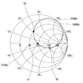
- the input impedance characteristic is at point A1 in the Smith chart shown in FIG.
- the accuracy when a coiled antenna is formed by quenching is ⁇ 250 ⁇ m.
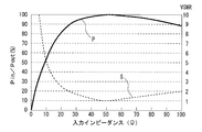
- the power / VSWR characteristics in these cases are as shown in FIG. 7.
- the input impedance of the antenna 1 changes to 10 ⁇ due to the contraction of the conductor. 44% of the power loss occurs.
- the vertical axis represents input power (Pin) / output power (Pout) and VSWR
- the horizontal axis represents input impedance
- P represents the Pin / Pout characteristic curve
- S represents the VSWR characteristic curve.
- An object of the present invention is to provide a coiled antenna capable of reducing errors during manufacture in view of the above-described problems.
- the present invention provides a first printed wiring board in which a plurality of linear printed wiring patterns are provided in parallel at predetermined intervals, and through holes are formed at both ends of each linear printed wiring pattern.
- a second printed wiring board in which a plurality of linear printed wiring patterns are provided in parallel at predetermined intervals and through holes are formed at both ends of each linear printed wiring pattern; the first printed wiring board;
- a plurality of linear printed wiring patterns formed on the printed wiring board are provided so as to be conductively connected in a spiral shape.
- Suggest antenna is composed of a sintered conductor.
- the linear printed wiring patterns formed on the two printed circuit boards are conductively connected in a spiral manner by the connecting conductors, and a coiled antenna is formed by the linear printed wiring patterns and the connecting conductors.
- the present invention fabricates a linear printed wiring pattern that constitutes an antenna element with conductive patterns on two printed wiring boards, and the conductive patterns of the first and second printed wiring boards are the first and second printed wirings. Since a spiral antenna element is formed by sequentially conducting conductive connections with through-hole conductors and connecting conductors provided on the substrate, the antenna is manufactured with dimensional accuracy of the printed wiring pattern and connecting conductors (for example, ⁇ 18 ⁇ m). Therefore, a high-performance antenna can be easily manufactured.
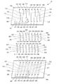
- FIG. 1 is an external perspective view showing an antenna according to an embodiment of the present invention.
- the disassembled perspective view which shows the antenna in one Embodiment of this invention.
- the plane perspective view showing the antenna in one embodiment of the present invention
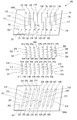
- the disassembled perspective view which shows the other structural example of the antenna in one Embodiment of this invention.
- External perspective view showing a conventional antenna Smith chart explaining impedance characteristics of conventional antenna The figure which shows the relationship of the impedance of an antenna of conventional example, and electric power and VSWR
- FIG. 1 is an external perspective view of an antenna according to an embodiment of the present invention
- FIG. 2 is an exploded perspective view thereof
- FIG. 3 is a plan perspective view thereof.
- reference numeral 10 denotes an antenna, which is composed of first and second printed wiring boards 100 and 200 and a plurality of columnar connecting conductors 311 to 318 and 321 to 328. Note that the antenna 10 in this embodiment has a resonance frequency of 315 MHz as in the conventional example.
- the first printed wiring board 100 is formed of a dielectric substrate having a rectangular shape with a predetermined area and a predetermined thickness, and a plurality of both sides in the width direction are spaced apart at predetermined equal intervals L3 on a straight line parallel to the long side.
- Through-holes 121 to 128, 131 to 138 are provided.
- the other through hole is arranged such that the through hole is disposed at a position substantially opposite to the center position of the gap between the through holes 121 to 128 provided on one side portion. 131 to 138 are provided.
- wiring patterns 111 to 118 are provided on the surface of the first printed wiring board 100 and arranged in parallel at equal intervals L3. Note that the width in the long side direction of the first printed wiring board 100 in each of the wiring patterns 111 to 118 is set to D2, and the length in the short side direction is set to L6.
- one end of the wiring pattern 111 is connected to the second through hole 122 from the end of one through hole 121 to 128, and the other end is a through hole 131 positioned at the end of the other through hole 131 to 138. It is connected to.
- One end of the wiring pattern 112 is connected to the third through hole 123 from the end in the row of one through holes 121 to 128, and the other end is a through hole located second from the end in the row of the other through holes 131 to 138. It is linked to 132.
- One end of the wiring pattern 113 is connected to the fourth through hole 124 from the end in the row of one through holes 121 to 128, and the other end is a through hole located third from the end in the row of the other through holes 131 to 138.
- One end of the wiring pattern 114 is connected to the fifth through hole 125 from the end in the row of one through holes 121 to 128, and the other end is the fourth through hole located from the end in the row of the other through holes 131 to 138. It is linked to 134.
- One end of the wiring pattern 115 is connected to the sixth through hole 126 from the end in the row of one through holes 121 to 128, and the other end is a through hole located fifth from the end in the row of the other through holes 131 to 138. It is linked to 135.
- One end of the wiring pattern 116 is connected to the seventh through hole 127 from the end of one through hole 121 to 128, and the other end is the sixth through hole from the end of the other through hole 131 to 138.
- One end of the wiring pattern 117 is connected to the eighth through hole 128 from the end of one through hole 121 to 128, and the other end is the seventh through hole located from the end of the other through hole 131 to 138. It is linked to 137.
- One end of the wiring pattern 118 is disposed at a position spaced from the one end of the wiring pattern 117 by an interval L3, and the other end is connected to the through hole 138 located at the eighth position from the end in the row of the other through holes 131 to 138. . As shown in FIG. 3, the distance between the first through hole 121 from the end and one end of the eighth wiring pattern 118 is set to L5.
- a feeding point 114a is set at a predetermined position of the fourth wiring pattern 114 from the end, and one end of the feeding wiring pattern 141 is conductively connected to this feeding point.
- the power supply wiring pattern 141 is provided so that the other end 142 reaches one short side of the first printed wiring board 100.
- the width of the power supply wiring pattern 141 at the power supply point 114a is set to D3.
- the power supply wiring pattern 141 is arranged so as to extend in the short side direction of the first printed wiring board 100, and is bent in the direction of 90 degrees to the right at a distance L 8 from one end of the wiring pattern 114.
- the width of the power supply wiring pattern 141 is set to D1.
- the second printed wiring board 200 has the same shape as the first printed wiring board 100, and a plurality of through holes 221 to 228,231 are formed on both sides in the width direction with a predetermined equal interval L3 on a straight line parallel to the long side. ⁇ 238 are provided. The positions of these through holes 221 to 228 and 231 to 238 correspond to the positions of the through holes 121 to 128 and 131 to 138 in the first printed wiring board 100.
- wiring patterns 211 to 218 are provided on the surface of the second printed wiring board 200 and arranged in parallel at equal intervals L3.
- the width in the long side direction of the second printed wiring board 200 in each of the wiring patterns 211 to 218 is set to D2, and the length in the short side direction is set to L6.
- One end of the wiring pattern 211 is connected to the first through hole 221 from the end of one through hole 221 to 228 row, and the other end is connected to the through hole 231 located at the end of the other through hole 231 to 238 row.
- One end of the wiring pattern 212 is connected to the second through hole 222 from the end of one through hole 221 to 228 row, and the other end is the through hole located second from the end of the other through hole 231 to 238 row.
- One end of the wiring pattern 213 is connected to the third through hole 223 from the end in the row of one through holes 221 to 228, and the other end is a through hole located third from the end in the row of the other through holes 231 to 238. It is linked to 233.
- One end of the wiring pattern 214 is connected to the fourth through hole 224 from the end of one through hole 221 to 228 row, and the other end is the fourth through hole located from the end of the other through hole 231 to 238 row.
- One end of the wiring pattern 215 is connected to the fifth through hole 225 from the end in the row of one through holes 221 to 228, and the other end is a through hole located fifth from the end in the row of the other through holes 231 to 238.
- One end of the wiring pattern 216 is connected to the sixth through hole 226 from the end in the row of one through holes 221 to 228, and the other end is a through hole located at the sixth from the end in the row of the other through holes 231 to 238. 236.
- One end of the wiring pattern 217 is connected to the seventh through hole 227 from the end in the row of one through holes 221 to 228, and the other end is a through hole located at the seventh from the end in the row of the other through holes 231 to 238. It is linked to 237.
- One end of the wiring pattern 218 is connected to the eighth through hole 228 from the end of one through hole 221 to 228 row, and the other end is the eighth through hole located from the end of the other through hole 231 to 238 row. 238.
- a feeding point 215a is set at a predetermined position of the fifth wiring pattern 215 from the end, and one end of the feeding wiring pattern 241 is conductively connected to this feeding point.
- the position of the feeding point 215a is set to a position facing the feeding point 114a of the wiring pattern 114 on the first printed wiring board 100.
- the power supply wiring pattern 241 is provided such that the other end 242 reaches one short side of the second printed wiring board 200 as shown in FIG. As shown in FIG. 3, the power supply wiring pattern 241 is formed in the same shape so as to face the power supply wiring pattern 141 formed on the first printed wiring board 100. Similar to the first printed circuit board 100, the width of the power supply wiring pattern 241 at the power supply point 215a is set to D3, and the power supply wiring pattern 241 extends in the short side direction of the second printed circuit board 200.
- the wiring pattern 214 is bent 90 degrees to the right at a distance L8 from the end of the wiring pattern 214, extended to the direction of the first through hole 221 by a distance L4, bent to the right 90 degrees, and extended to the left by a distance L1. It reaches the short side of the second printed wiring board 200 at a position where it is bent 90 degrees and extended by the distance L2.
- the width of the power supply wiring pattern 241 is set to D1.
- the wiring patterns 111 to 118 of the first printed wiring board 100 and the wiring patterns 211 to 218 of the second printed wiring board 200 are conductively connected by a plurality of connecting conductors 311 to 318 and 321 to 328 so as to be spiral.
- cylindrical conductors having a diameter of 0.75 mm and a length of 8.0 mm are used as the connecting conductors 311 to 318 and 321 to 328.
- the respective one ends 311a to 318a of the connecting conductors 311 to 318 are inserted and fixed in the through holes 121 to 128 of the first printed wiring board 100, and the respective one ends 312a to 318a of the connecting conductors 312 to 318 are connected to the wiring pattern 111.
- Conductive connection is made to one end of .about.117.
- the other ends 311b to 318b of the connecting conductors 311 to 318 are inserted and fixed in the through holes 221 to 228 of the second printed wiring board 200, and the other ends 311b to 318b of the connecting conductors 311 to 318 are wired.
- Conductive connections are made to one end of the patterns 211-218.
- the respective one ends 321a to 328a of the connecting conductors 321 to 328 are inserted and fixed in the through holes 131 to 138 of the first printed wiring board 100, and the respective one ends 321a to 328a of the connecting conductors 321 to 328 are connected to the wiring pattern 111.
- the other end of .about.118 is conductively connected.
- the other ends 321b to 328b of the connection conductors 321 to 328 are inserted and fixed in the through holes 231 to 238 of the second printed wiring board 200, and the other ends 321b to 328b of the connection conductors 321 to 328 are wired.
- the other ends of the patterns 211 to 218 are conductively connected.
- L1 5.0 mm
- L2 5.0 mm
- L3 1.726 mm
- L4 12.9 mm
- L5 21.81 mm
- L6 17.75 mm
- L7 4.375 mm
- L8 2.3 mm
- D1 0.5 mm
- D2 1.0 mm
- D3 1.5 mm.
- the antenna elements are formed by the conductive wiring patterns 111 to 118 and 211 to 218 on the two printed wiring boards 100 and 200, and these wiring patterns 111 to 118 and 211 to 218 are connected by the connecting conductors 311 to 318 and 321 to 328.
- a helical antenna element is formed by alternately conducting conductive connections.
- the antenna can be manufactured with the dimensional accuracy of the printed wiring patterns 111 to 118 and 211 to 218 and the dimensional accuracy of the connecting conductors 311 to 318 and 321 to 328 (for example, ⁇ 18 ⁇ m), and a high-performance antenna can be easily manufactured.
- mass production is easy and high reliability can be achieved in electrical connection to a printed wiring board, and an antenna with excellent dimensional accuracy can be easily manufactured.
- the power supply wiring patterns 141 and 241 are provided on the same surface as the wiring patterns 111 to 118 and 211 to 218.
- the wiring patterns 111 to 118 and 211 to 218 are arranged on the printed wiring boards 100 and 200 as in the antenna 10A shown in FIG.
- the power supply wiring patterns 141 and 241 may be provided on the back surface of the printed wiring boards 100 and 200 and may be conductively connected by the through-hole conductors 161 and 261.
- the antenna having the feeding point at the middle portion of the coil is configured. However, it goes without saying that the same effect as described above can be obtained when the antenna having the feeding point at the coil end portion is configured.
Abstract
Provided is a coil shaped antenna wherein errors at the time of production can be reduced.
An antenna (10) is constituted by providing connection conductors wherein the opposite ends of the connection conductors are connected to through holes formed on first and second printed wiring boards (100, 200) so that the first printed wiring board (100) is opposed to the second printed wiring board (200), and the connection conductors helically and conductively connect a plurality of linear printed wiring patterns (111 to 118) formed on the first printed wiring board (100) and a plurality of linear printed wiring patterns (211 to 218) formed on the second printed wiring board (200).
Description
本発明は、アンテナに関し、特に、コイル状のヘリカルアンテナに関するものである。
The present invention relates to an antenna, and more particularly to a coiled helical antenna.
従来、ヘリカルアンテナを制作する場合、銅線などの金属材料を螺旋状に折り曲げた形状で、スプリング(バネ)と同じ制作方法を用いている。スプリングは折り曲げただけでは形状保持が難しいため、高温で焼き入れをするのが一般的である。
Conventionally, when producing a helical antenna, a metal material such as a copper wire is folded in a spiral shape, and the same production method as a spring is used. Since it is difficult to maintain the shape of the spring simply by bending it, it is generally hardened at a high temperature.
このようなコイル状のヘリカルアンテナは、例えば特開2001-345628号公報(特許文献1)及び特開2006-340186号公報(特許文献2)に開示されるように小型のアンテナとして有効に利用されている。
Such a coiled helical antenna is effectively used as a small antenna as disclosed in, for example, Japanese Patent Application Laid-Open No. 2001-345628 (Patent Document 1) and Japanese Patent Application Laid-Open No. 2006-340186 (Patent Document 2). ing.
しかしながら、前述したように、アンテナを作成するにはスプリングは折り曲げただけでは形状保持が難しいため、高温で焼き入れをするのが一般的である。このため、焼き入れによる材料の収縮などにより、特に小型アンテナの性能を満足する要求精度(例えば±20μm)を実現することは困難であった。なお、ここでの要求精度とはVSWRが2以下となる精度を意味する。
However, as described above, in order to create an antenna, it is difficult to maintain the shape by simply bending the spring, and therefore it is common to perform quenching at a high temperature. For this reason, it has been difficult to achieve the required accuracy (for example, ± 20 μm) that satisfies the performance of a small antenna due to shrinkage of the material due to quenching. The required accuracy here means the accuracy with which VSWR is 2 or less.
例えば、図5に示すような整合周波数が315MHzで整合入力インピーダンスが50Ωの巻回数10のコイル状のアンテナ1を作成した場合、焼き入れ前の寸法はコイルの直径Dが12.500mm、コイルの長さHが12.442mm、給電線の長さLが38mmであり、入力インピーダンス特性は図6に示すスミスチャートにおけるA1の点にある。しかし、焼き入れを行った後は導体の収縮によってコイルの寸法が変わってしまう。一般的に、焼き入れをしてコイル状のアンテナを作成した場合の精度は±250μmである。
For example, when a coiled antenna 1 having a winding frequency of 315 MHz and a matching input impedance of 50Ω as shown in FIG. 5 and having a winding number of 10 is prepared, the coil diameter D is 12.500 mm before quenching. The length H is 12.442 mm, the length L of the feeder line is 38 mm, and the input impedance characteristic is at point A1 in the Smith chart shown in FIG. However, after quenching, the coil dimensions change due to the contraction of the conductor. In general, the accuracy when a coiled antenna is formed by quenching is ± 250 μm.
この場合、VSWRが2よりも大きくなるとき、例えばコイル状のアンテナ1の長さHが±20μmを超えた場合はアンテナ1の入力インピーダンスが大きく変化して、アンテナ特性が悪化する。すなわち、焼き入れによってアンテナ1の長さHが12,422mm(VSWR=2)に変わったときの入力インピーダンス特性は図6に示すスミスチャートにおけるB1の点にあり、焼き入れによってアンテナ1の長さH1が12,462mm(VSWR=2)に変わったときの入力インピーダンス特性は図6に示すスミスチャートにおけるB2の点にある。これらの場合の電力・VSWR特性は図7に示すようになり、例えばアンテナ1の最適入力インピーダンス値が50Ωであるのに対して、導体の収縮によりアンテナ1の入力インピーダンスが10Ωに変化したときは、44%の電力損失が生じてしまう。なお、図7において、縦軸は入力電力(Pin)/出力電力(Pout)とVSWRを表し、横軸は入力インピーダンスを表し、PはPin/Pout特性曲線、SはVSWR特性曲線をそれぞれ表している。
In this case, when the VSWR is larger than 2, for example, when the length H of the coiled antenna 1 exceeds ± 20 μm, the input impedance of the antenna 1 is greatly changed, and the antenna characteristics are deteriorated. That is, the input impedance characteristic when the length H of the antenna 1 is changed to 12,422 mm (VSWR = 2) by quenching is at the point B1 in the Smith chart shown in FIG. 6, and the length of the antenna 1 by quenching. The input impedance characteristic when H1 is changed to 12,462 mm (VSWR = 2) is at point B2 in the Smith chart shown in FIG. The power / VSWR characteristics in these cases are as shown in FIG. 7. For example, when the optimum input impedance value of the antenna 1 is 50Ω, the input impedance of the antenna 1 changes to 10Ω due to the contraction of the conductor. 44% of the power loss occurs. In FIG. 7, the vertical axis represents input power (Pin) / output power (Pout) and VSWR, the horizontal axis represents input impedance, P represents the Pin / Pout characteristic curve, and S represents the VSWR characteristic curve. Yes.
本発明の目的は、上記の問題点に鑑み、製造時の誤差を少なくできるコイル状のアンテナを提供することである。
An object of the present invention is to provide a coiled antenna capable of reducing errors during manufacture in view of the above-described problems.
本発明は、上記の問題点に鑑み、所定間隔をあけて平行に直線状プリント配線パターンが複数設けられ且つ各直線状プリント配線パターンの両端にスルーホールが形成されている第1プリント配線基板と、所定間隔をあけて平行に直線状プリント配線パターンが複数設けられ且つ各直線状プリント配線パターンの両端にスルーホールが形成されている第2プリント配線基板と、前記第1プリント配線基板と前記第2プリント配線基板が対向するように前記第1及び第2プリント配線基板に形成されたスルーホールに両端が連結され且つ前記第1プリント配線基板に形成された複数の直線状プリント配線パターンと前記第2プリント配線基板に形成された複数の直線状プリント配線パターンが螺旋状に導電接続されるように設けられた複数の連結導体とから構成されているアンテナを提案する。
In view of the above problems, the present invention provides a first printed wiring board in which a plurality of linear printed wiring patterns are provided in parallel at predetermined intervals, and through holes are formed at both ends of each linear printed wiring pattern. A second printed wiring board in which a plurality of linear printed wiring patterns are provided in parallel at predetermined intervals and through holes are formed at both ends of each linear printed wiring pattern; the first printed wiring board; A plurality of linear printed wiring patterns formed on the first printed wiring board and connected to through holes formed in the first and second printed wiring boards so that two printed wiring boards face each other; 2 A plurality of linear printed wiring patterns formed on the printed wiring board are provided so as to be conductively connected in a spiral shape. Suggest antenna is composed of a sintered conductor.
本発明により、2つのプリント基板のそれぞれに形成された直線状プリント配線パターンは連結導体によって螺旋状に導電接続され、これらの直線状プリント配線パターンと連結導体によってコイル状のアンテナが形成される。
According to the present invention, the linear printed wiring patterns formed on the two printed circuit boards are conductively connected in a spiral manner by the connecting conductors, and a coiled antenna is formed by the linear printed wiring patterns and the connecting conductors.
本発明は、2つのプリント配線基板上に導電性パターンでアンテナエレメントを構成する直線状プリント配線パターンを製作し、第1及び第2プリント配線基板の導電性パターンは、第1及び第2プリント配線基板に設けたスルーホール導体及び連結導体により順次交互に導電接続されて螺旋状のアンテナエレメントが構成されるので、プリント配線パターンの寸法精度及び連結導体の寸法精度(例えば±18μm)によるアンテナの製作が実現できるため、高性能なアンテナを容易に製作することができる。
The present invention fabricates a linear printed wiring pattern that constitutes an antenna element with conductive patterns on two printed wiring boards, and the conductive patterns of the first and second printed wiring boards are the first and second printed wirings. Since a spiral antenna element is formed by sequentially conducting conductive connections with through-hole conductors and connecting conductors provided on the substrate, the antenna is manufactured with dimensional accuracy of the printed wiring pattern and connecting conductors (for example, ± 18 μm). Therefore, a high-performance antenna can be easily manufactured.
10,10A…アンテナ、100…第1プリント配線基板、111~118…直線状プリント配線パターン、121~128,131~138…スルーホール、114a…給電点、141…給電用配線パターン、161…スルーホール導体、200…第2プリント配線基板、211~218…直線状プリント配線パターン、221~228,231~238…スルーホール、215a…給電点、241…給電用配線パターン、261…スルーホール導体、311~318,321~328…連結導体。
10, 10A ... Antenna, 100 ... First printed wiring board, 111-118 ... Linear printed wiring pattern, 121-128, 131-138 ... Through-hole, 114a ... Feeding point, 141 ... Feeding wiring pattern, 161 ... Through-hole conductor , 200 ... second printed wiring board, 211-218 ... linear printed wiring pattern, 221-228,231-238 ... through hole, 215a ... feed point, 241 ... feeding wiring pattern, 261 ... through hole conductor, 311-318,321- 328 ... Connecting conductor.
以下、図面を参照して本発発明の一実施形態を説明する。
Hereinafter, an embodiment of the present invention will be described with reference to the drawings.
図1は本発明の一実施形態におけるアンテナの外観斜視図、図2はその分解斜視図、図3はその平面透視図である。図において、10はアンテナで、第1及び第2プリント配線基板100,200と複数の円柱状の連結導体311~318,321~328から構成されている。なお、本実施形態におけるアンテナ10は従来例と同様に315MHzを共振周波数とするものである。
1 is an external perspective view of an antenna according to an embodiment of the present invention, FIG. 2 is an exploded perspective view thereof, and FIG. 3 is a plan perspective view thereof. In the figure, reference numeral 10 denotes an antenna, which is composed of first and second printed wiring boards 100 and 200 and a plurality of columnar connecting conductors 311 to 318 and 321 to 328. Note that the antenna 10 in this embodiment has a resonance frequency of 315 MHz as in the conventional example.
第1プリント配線基板100は所定面積の長方形をなすとともに所定の厚みを有する誘電体基板からなり、幅方向の両側辺部には長辺と平行な直線上に所定の等間隔L3をあけて複数のスルーホール121~128,131~138が設けられている。また、図3に示すように、一方の側辺部に設けられたスルーホール121~128のスルーホール間の間隙のほぼ中央位置と対向する位置にスルーホールが配置されるように他方のスルーホール131~138が設けられている。
The first printed wiring board 100 is formed of a dielectric substrate having a rectangular shape with a predetermined area and a predetermined thickness, and a plurality of both sides in the width direction are spaced apart at predetermined equal intervals L3 on a straight line parallel to the long side. Through-holes 121 to 128, 131 to 138 are provided. In addition, as shown in FIG. 3, the other through hole is arranged such that the through hole is disposed at a position substantially opposite to the center position of the gap between the through holes 121 to 128 provided on one side portion. 131 to 138 are provided.
さらに、第1プリント配線基板100の表面には互いに等間隔L3をあけて平行に配置された複数の直線状プリント配線パターン(以下、配線パターンと称する)111~118が設けられている。なお、各配線パターン111~118における第1プリント配線基板100の長辺方向の幅はD2に設定され、短辺方向の長さはL6に設定されている。
Furthermore, a plurality of linear printed wiring patterns (hereinafter referred to as wiring patterns) 111 to 118 are provided on the surface of the first printed wiring board 100 and arranged in parallel at equal intervals L3. Note that the width in the long side direction of the first printed wiring board 100 in each of the wiring patterns 111 to 118 is set to D2, and the length in the short side direction is set to L6.
また、配線パターン111の一端は一方のスルーホール121~128の列における端から2番目のスルーホール122に連結され、他端は他方のスルーホール131~138の列における端に位置するスルーホール131に連結されている。配線パターン112の一端は一方のスルーホール121~128の列における端から3番目のスルーホール123に連結され、他端は他方のスルーホール131~138の列における端から2番目に位置するスルーホール132に連結されている。配線パターン113の一端は一方のスルーホール121~128の列における端から4番目のスルーホール124に連結され、他端は他方のスルーホール131~138の列における端から3番目に位置するスルーホール133に連結されている。配線パターン114の一端は一方のスルーホール121~128の列における端から5番目のスルーホール125に連結され、他端は他方のスルーホール131~138の列における端から4番目に位置するスルーホール134に連結されている。配線パターン115の一端は一方のスルーホール121~128の列における端から6番目のスルーホール126に連結され、他端は他方のスルーホール131~138の列における端から5番目に位置するスルーホール135に連結されている。配線パターン116の一端は一方のスルーホール121~128の列における端から7番目のスルーホール127に連結され、他端は他方のスルーホール131~138の列における端から6番目に位置するスルーホール136に連結されている。配線パターン117の一端は一方のスルーホール121~128の列における端から8番目のスルーホール128に連結され、他端は他方のスルーホール131~138の列における端から7番目に位置するスルーホール137に連結されている。配線パターン118の一端は配線パターン117の一端から間隔L3をあけた位置に配置され、他端は他方のスルーホール131~138の列における端から8番目に位置するスルーホール138に連結されている。なお、図3に示すように、端から1番目のスルーホール121と8番目の配線パターン118の一端との間の距離はL5に設定されている。
In addition, one end of the wiring pattern 111 is connected to the second through hole 122 from the end of one through hole 121 to 128, and the other end is a through hole 131 positioned at the end of the other through hole 131 to 138. It is connected to. One end of the wiring pattern 112 is connected to the third through hole 123 from the end in the row of one through holes 121 to 128, and the other end is a through hole located second from the end in the row of the other through holes 131 to 138. It is linked to 132. One end of the wiring pattern 113 is connected to the fourth through hole 124 from the end in the row of one through holes 121 to 128, and the other end is a through hole located third from the end in the row of the other through holes 131 to 138. It is linked to 133. One end of the wiring pattern 114 is connected to the fifth through hole 125 from the end in the row of one through holes 121 to 128, and the other end is the fourth through hole located from the end in the row of the other through holes 131 to 138. It is linked to 134. One end of the wiring pattern 115 is connected to the sixth through hole 126 from the end in the row of one through holes 121 to 128, and the other end is a through hole located fifth from the end in the row of the other through holes 131 to 138. It is linked to 135. One end of the wiring pattern 116 is connected to the seventh through hole 127 from the end of one through hole 121 to 128, and the other end is the sixth through hole from the end of the other through hole 131 to 138. It is linked to 136. One end of the wiring pattern 117 is connected to the eighth through hole 128 from the end of one through hole 121 to 128, and the other end is the seventh through hole located from the end of the other through hole 131 to 138. It is linked to 137. One end of the wiring pattern 118 is disposed at a position spaced from the one end of the wiring pattern 117 by an interval L3, and the other end is connected to the through hole 138 located at the eighth position from the end in the row of the other through holes 131 to 138. . As shown in FIG. 3, the distance between the first through hole 121 from the end and one end of the eighth wiring pattern 118 is set to L5.
さらに、端から4番目の配線パターン114の所定位置に給電点114aが設定され、この給電点に給電用配線パターン141の一端が導電接続されている。給電用配線パターン141は、図に示すようにその他端142が第1プリント配線基板100の一方の短辺に至るように設けられている。なお、図3に示すように、給電点114aにおける給電用配線パターン141の幅はD3に設定されている。さらに、給電用配線パターン141は、第1プリント配線基板100の短辺方向に延ばして配置され、配線パターン114の一端から距離L8の位置において右90度方向に折り曲げられ1番目のスルーホール121の方向に距離L4延ばされて右90度方向に折り曲げられ、距離L1延ばされた後に左90度方向に折り曲げられて距離L2延ばされた位置において第1プリント配線基板100の短辺に至る。また、給電用配線パターン141の幅はD1に設定されている。
Furthermore, a feeding point 114a is set at a predetermined position of the fourth wiring pattern 114 from the end, and one end of the feeding wiring pattern 141 is conductively connected to this feeding point. As shown in the drawing, the power supply wiring pattern 141 is provided so that the other end 142 reaches one short side of the first printed wiring board 100. As shown in FIG. 3, the width of the power supply wiring pattern 141 at the power supply point 114a is set to D3. Further, the power supply wiring pattern 141 is arranged so as to extend in the short side direction of the first printed wiring board 100, and is bent in the direction of 90 degrees to the right at a distance L 8 from one end of the wiring pattern 114. It is extended in the direction by a distance L4 and bent in the direction of 90 degrees to the right, and after extending the distance L1 and then bent in the direction of 90 degrees to the left and extended in the distance L2, it reaches the short side of the first printed wiring board 100. . The width of the power supply wiring pattern 141 is set to D1.
第2プリント配線基板200は第1プリント配線基板100と同じ形状をなし、幅方向の両側辺部には長辺と平行な直線上に所定の等間隔L3をあけて複数のスルーホール221~228,231~238が設けられている。これらのスルーホール221~228,231~238の位置は、第1プリント配線基板100におけるスルーホール121~128,131~138の位置に対応する。
The second printed wiring board 200 has the same shape as the first printed wiring board 100, and a plurality of through holes 221 to 228,231 are formed on both sides in the width direction with a predetermined equal interval L3 on a straight line parallel to the long side. ~ 238 are provided. The positions of these through holes 221 to 228 and 231 to 238 correspond to the positions of the through holes 121 to 128 and 131 to 138 in the first printed wiring board 100.
さらに、第2プリント配線基板200の表面には互いに等間隔L3をあけて平行に配置された複数の直線状プリント配線パターン(以下、配線パターンと称する)211~218が設けられている。なお、各配線パターン211~218における第2プリント配線基板200の長辺方向の幅はD2に設定され、短辺方向の長さはL6に設定されている。
Furthermore, a plurality of linear printed wiring patterns (hereinafter referred to as wiring patterns) 211 to 218 are provided on the surface of the second printed wiring board 200 and arranged in parallel at equal intervals L3. The width in the long side direction of the second printed wiring board 200 in each of the wiring patterns 211 to 218 is set to D2, and the length in the short side direction is set to L6.
配線パターン211の一端は一方のスルーホール221~228の列における端から1番目のスルーホール221に連結され、他端は他方のスルーホール231~238の列における端に位置するスルーホール231に連結されている。配線パターン212の一端は一方のスルーホール221~228の列における端から2番目のスルーホール222に連結され、他端は他方のスルーホール231~238の列における端から2番目に位置するスルーホール232に連結されている。配線パターン213の一端は一方のスルーホール221~228の列における端から3番目のスルーホール223に連結され、他端は他方のスルーホール231~238の列における端から3番目に位置するスルーホール233に連結されている。配線パターン214の一端は一方のスルーホール221~228の列における端から4番目のスルーホール224に連結され、他端は他方のスルーホール231~238の列における端から4番目に位置するスルーホール234に連結されている。配線パターン215の一端は一方のスルーホール221~228の列における端から5番目のスルーホール225に連結され、他端は他方のスルーホール231~238の列における端から5番目に位置するスルーホール235に連結されている。配線パターン216の一端は一方のスルーホール221~228の列における端から6番目のスルーホール226に連結され、他端は他方のスルーホール231~238の列における端から6番目に位置するスルーホール236に連結されている。配線パターン217の一端は一方のスルーホール221~228の列における端から7番目のスルーホール227に連結され、他端は他方のスルーホール231~238の列における端から7番目に位置するスルーホール237に連結されている。配線パターン218の一端は一方のスルーホール221~228の列における端から8番目のスルーホール228に連結され、他端は他方のスルーホール231~238の列における端から8番目に位置するスルーホール238に連結されている。
One end of the wiring pattern 211 is connected to the first through hole 221 from the end of one through hole 221 to 228 row, and the other end is connected to the through hole 231 located at the end of the other through hole 231 to 238 row. Has been. One end of the wiring pattern 212 is connected to the second through hole 222 from the end of one through hole 221 to 228 row, and the other end is the through hole located second from the end of the other through hole 231 to 238 row. 232. One end of the wiring pattern 213 is connected to the third through hole 223 from the end in the row of one through holes 221 to 228, and the other end is a through hole located third from the end in the row of the other through holes 231 to 238. It is linked to 233. One end of the wiring pattern 214 is connected to the fourth through hole 224 from the end of one through hole 221 to 228 row, and the other end is the fourth through hole located from the end of the other through hole 231 to 238 row. 234. One end of the wiring pattern 215 is connected to the fifth through hole 225 from the end in the row of one through holes 221 to 228, and the other end is a through hole located fifth from the end in the row of the other through holes 231 to 238. 235. One end of the wiring pattern 216 is connected to the sixth through hole 226 from the end in the row of one through holes 221 to 228, and the other end is a through hole located at the sixth from the end in the row of the other through holes 231 to 238. 236. One end of the wiring pattern 217 is connected to the seventh through hole 227 from the end in the row of one through holes 221 to 228, and the other end is a through hole located at the seventh from the end in the row of the other through holes 231 to 238. It is linked to 237. One end of the wiring pattern 218 is connected to the eighth through hole 228 from the end of one through hole 221 to 228 row, and the other end is the eighth through hole located from the end of the other through hole 231 to 238 row. 238.
さらに、端から5番目の配線パターン215の所定位置に給電点215aが設定され、この給電点に給電用配線パターン241の一端が導電接続されている。なお、給電点215aの位置は、第1プリント配線基板100における配線パターン114の給電点114aに対向する位置に設定されている。
Further, a feeding point 215a is set at a predetermined position of the fifth wiring pattern 215 from the end, and one end of the feeding wiring pattern 241 is conductively connected to this feeding point. The position of the feeding point 215a is set to a position facing the feeding point 114a of the wiring pattern 114 on the first printed wiring board 100.
給電用配線パターン241は、図2に示すようにその他端242が第2プリント配線基板200の一方の短辺に至るように設けられている。なお、図3に示すように、給電用配線パターン241は第1プリント配線基板100に形成されている給電用配線パターン141に対向するように同形状に形成されている。なお、第1プリント配線基板100と同様に、給電点215aにおける給電用配線パターン241の幅はD3に設定され、給電用配線パターン241は第2プリント配線基板200の短辺方向に延ばして配置され、配線パターン214の一端から距離L8の位置において右90度方向に折り曲げられ1番目のスルーホール221の方向に距離L4延ばされて右90度方向に折り曲げられ、距離L1延ばされた後に左90度方向に折り曲げられて距離L2延ばされた位置において第2プリント配線基板200の短辺に至る。また、給電用配線パターン241の幅はD1に設定されている。
The power supply wiring pattern 241 is provided such that the other end 242 reaches one short side of the second printed wiring board 200 as shown in FIG. As shown in FIG. 3, the power supply wiring pattern 241 is formed in the same shape so as to face the power supply wiring pattern 141 formed on the first printed wiring board 100. Similar to the first printed circuit board 100, the width of the power supply wiring pattern 241 at the power supply point 215a is set to D3, and the power supply wiring pattern 241 extends in the short side direction of the second printed circuit board 200. The wiring pattern 214 is bent 90 degrees to the right at a distance L8 from the end of the wiring pattern 214, extended to the direction of the first through hole 221 by a distance L4, bent to the right 90 degrees, and extended to the left by a distance L1. It reaches the short side of the second printed wiring board 200 at a position where it is bent 90 degrees and extended by the distance L2. The width of the power supply wiring pattern 241 is set to D1.
第1プリント配線基板100の配線パターン111~118と第2プリント配線基板200の配線パターン211~218とは複数の連結導体311~318,321~328によって全体が螺旋状になるように導電接続されている。本実施形態では、連結導体311~318,321~328として、直径0.75mm、長さ8.0mmの円柱状導体を用いている。
The wiring patterns 111 to 118 of the first printed wiring board 100 and the wiring patterns 211 to 218 of the second printed wiring board 200 are conductively connected by a plurality of connecting conductors 311 to 318 and 321 to 328 so as to be spiral. . In this embodiment, cylindrical conductors having a diameter of 0.75 mm and a length of 8.0 mm are used as the connecting conductors 311 to 318 and 321 to 328.
すなわち、連結導体311~318のそれぞれの一端311a~318aは第1プリント配線基板100のスルーホール121~128に挿入されて固定され、連結導体312~318のそれぞれの一端312a~318aが配線パターン111~117の一端に導電接続されている。さらに、連結導体311~318のそれぞれの他端311b~318bは第2プリント配線基板200のスルーホール221~228に挿入されて固定され、連結導体311~318のそれぞれの他端311b~318bが配線パターン211~218の一端に導電接続されている。また、連結導体321~328のそれぞれの一端321a~328aは第1プリント配線基板100のスルーホール131~138に挿入されて固定され、連結導体321~328のそれぞれの一端321a~328aが配線パターン111~118の他端に導電接続されている。さらに、連結導体321~328のそれぞれの他端321b~328bは第2プリント配線基板200のスルーホール231~238に挿入されて固定され、連結導体321~328のそれぞれの他端321b~328bが配線パターン211~218の他端に導電接続されている。
That is, the respective one ends 311a to 318a of the connecting conductors 311 to 318 are inserted and fixed in the through holes 121 to 128 of the first printed wiring board 100, and the respective one ends 312a to 318a of the connecting conductors 312 to 318 are connected to the wiring pattern 111. Conductive connection is made to one end of .about.117. Further, the other ends 311b to 318b of the connecting conductors 311 to 318 are inserted and fixed in the through holes 221 to 228 of the second printed wiring board 200, and the other ends 311b to 318b of the connecting conductors 311 to 318 are wired. Conductive connections are made to one end of the patterns 211-218. Also, the respective one ends 321a to 328a of the connecting conductors 321 to 328 are inserted and fixed in the through holes 131 to 138 of the first printed wiring board 100, and the respective one ends 321a to 328a of the connecting conductors 321 to 328 are connected to the wiring pattern 111. The other end of .about.118 is conductively connected. Further, the other ends 321b to 328b of the connection conductors 321 to 328 are inserted and fixed in the through holes 231 to 238 of the second printed wiring board 200, and the other ends 321b to 328b of the connection conductors 321 to 328 are wired. The other ends of the patterns 211 to 218 are conductively connected.
なお、本実施形態では、一例としてL1=5.0mm、L2=5.0mm、L3=1.726mm、L4=12.9mm、L5=21.81mm、L6=17.75mm、L7=4.375mm、L8=2.3mm、D1=0.5mm、D2=1.0mm、D3=1.5mmにそれぞれ設定している。
In this embodiment, as an example, L1 = 5.0 mm, L2 = 5.0 mm, L3 = 1.726 mm, L4 = 12.9 mm, L5 = 21.81 mm, L6 = 17.75 mm, L7 = 4.375 mm. L8 = 2.3 mm, D1 = 0.5 mm, D2 = 1.0 mm, and D3 = 1.5 mm.
上記実施形態によれば、2つのプリント配線基板100,200上に導電性の配線パターン111~118,211~218でアンテナエレメントが形成され、これらの配線パターン111~118,211~218は連結導体311~318,321~328によって順次交互に導電接続されて螺旋状のアンテナエレメントが構成される。これにより、プリント配線パターン111~118,211~218の寸法精度及び連結導体311~318,321~328の寸法精度(例えば±18μm)によるアンテナ製作が実現でき、且つ高性能なアンテナを容易に製作することができる。さらに、大量生産が容易であると共にプリント配線基板への電気的接続において高い信頼性を達成でき寸法精度に優れたアンテナを容易に製作することができる。
According to the above embodiment, the antenna elements are formed by the conductive wiring patterns 111 to 118 and 211 to 218 on the two printed wiring boards 100 and 200, and these wiring patterns 111 to 118 and 211 to 218 are connected by the connecting conductors 311 to 318 and 321 to 328. A helical antenna element is formed by alternately conducting conductive connections. As a result, the antenna can be manufactured with the dimensional accuracy of the printed wiring patterns 111 to 118 and 211 to 218 and the dimensional accuracy of the connecting conductors 311 to 318 and 321 to 328 (for example, ± 18 μm), and a high-performance antenna can be easily manufactured. . In addition, mass production is easy and high reliability can be achieved in electrical connection to a printed wiring board, and an antenna with excellent dimensional accuracy can be easily manufactured.
なお、上記実施形態では給電用配線パターン141,241を配線パターン111~118,211~218と同じ面に設けたが、図4に示すアンテナ10Aのように、配線パターン111~118,211~218をプリント配線基板100,200の表面に設け、給電用配線パターン141,241をプリント配線基板100,200の裏面に設け、これらをスルーホール導体161,261によって導電接続するようにしても良い。また、本実施形態ではコイルの中間部に給電点を有するアンテナを構成したがコイル端部に給電点を有するアンテナを構成する場合も上記同様の効果を奏することは言うまでもない。
In the above embodiment, the power supply wiring patterns 141 and 241 are provided on the same surface as the wiring patterns 111 to 118 and 211 to 218. However, the wiring patterns 111 to 118 and 211 to 218 are arranged on the printed wiring boards 100 and 200 as in the antenna 10A shown in FIG. The power supply wiring patterns 141 and 241 may be provided on the back surface of the printed wiring boards 100 and 200 and may be conductively connected by the through- hole conductors 161 and 261. Further, in the present embodiment, the antenna having the feeding point at the middle portion of the coil is configured. However, it goes without saying that the same effect as described above can be obtained when the antenna having the feeding point at the coil end portion is configured.
Claims (3)
- 所定間隔をあけて平行に直線状プリント配線パターンが複数設けられ且つ各直線状プリント配線パターンの両端にスルーホールが形成されている第1プリント配線基板と、
所定間隔をあけて平行に直線状プリント配線パターンが複数設けられ且つ各直線状プリント配線パターンの両端にスルーホールが形成されている第2プリント配線基板と、
前記第1プリント配線基板と前記第2プリント配線基板が対向するように前記第1及び第2プリント配線基板に形成されたスルーホールに両端が連結され且つ前記第1プリント配線基板に形成された複数の直線状プリント配線パターンと前記第2プリント配線基板に形成された複数の直線状プリント配線パターンが螺旋状に導電接続されるように設けられた複数の連結導体とから構成されている
ことを特徴とするアンテナ。 A first printed wiring board in which a plurality of linear printed wiring patterns are provided in parallel with a predetermined interval and through holes are formed at both ends of each linear printed wiring pattern;
A second printed wiring board in which a plurality of linear printed wiring patterns are provided in parallel at a predetermined interval and through holes are formed at both ends of each linear printed wiring pattern;
A plurality of pins formed on the first printed wiring board and connected at both ends to through holes formed in the first and second printed wiring boards so that the first printed wiring board and the second printed wiring board are opposed to each other. And a plurality of connecting conductors provided so that the plurality of linear printed wiring patterns formed on the second printed wiring board are spirally conductively connected. And antenna. - 前記第1及び第2プリント配線基板の表面に前記直線状プリント配線パターンが設けられ且つ裏面に給電部を構成する配線パターンが設けられ、前記表面の直線状プリント配線パターンの所定位置と前記裏面の給電部を構成する配線パターンがスルーホール導体によって導電接続されている
ことを特徴とする請求項1に記載のアンテナ。 The linear printed wiring pattern is provided on the front surface of the first and second printed wiring boards, and the wiring pattern constituting the power feeding portion is provided on the back surface, and a predetermined position of the linear printed wiring pattern on the front surface and The antenna according to claim 1, wherein the wiring pattern constituting the power feeding portion is conductively connected by a through-hole conductor. - 前記第1及び第2プリント配線基板に設けられた複数の直線状プリント配線パターンと前記複数の連結導体とからなるコイルの一端と他端との間の所定位置に所定インピーダンスの給電点が設定されている
ことを特徴とする請求項1又は2に記載のアンテナ。 A feeding point having a predetermined impedance is set at a predetermined position between one end and the other end of a coil composed of a plurality of linear printed wiring patterns provided on the first and second printed wiring boards and the plurality of connecting conductors. The antenna according to claim 1 or 2, wherein the antenna is provided.
Priority Applications (3)
| Application Number | Priority Date | Filing Date | Title |
|---|---|---|---|
| US13/393,058 US8253646B2 (en) | 2009-09-01 | 2010-06-10 | Antenna |
| EP10813554.2A EP2475043B1 (en) | 2009-09-01 | 2010-06-10 | Antenna |
| CN201080038786.6A CN102484319B (en) | 2009-09-01 | 2010-06-10 | Antenna |
Applications Claiming Priority (2)
| Application Number | Priority Date | Filing Date | Title |
|---|---|---|---|
| JP2009-201573 | 2009-09-01 | ||
| JP2009201573A JP4748334B2 (en) | 2009-09-01 | 2009-09-01 | antenna |
Publications (1)
| Publication Number | Publication Date |
|---|---|
| WO2011027603A1 true WO2011027603A1 (en) | 2011-03-10 |
Family
ID=43649154
Family Applications (1)
| Application Number | Title | Priority Date | Filing Date |
|---|---|---|---|
| PCT/JP2010/059813 WO2011027603A1 (en) | 2009-09-01 | 2010-06-10 | Antenna |
Country Status (5)
| Country | Link |
|---|---|
| US (1) | US8253646B2 (en) |
| EP (1) | EP2475043B1 (en) |
| JP (1) | JP4748334B2 (en) |
| CN (1) | CN102484319B (en) |
| WO (1) | WO2011027603A1 (en) |
Cited By (1)
| Publication number | Priority date | Publication date | Assignee | Title |
|---|---|---|---|---|
| WO2016143584A1 (en) * | 2015-03-09 | 2016-09-15 | 株式会社村田製作所 | Coil device and electronic device |
Families Citing this family (6)
| Publication number | Priority date | Publication date | Assignee | Title |
|---|---|---|---|---|
| CN103025545B (en) * | 2010-12-02 | 2016-06-22 | 横滨橡胶株式会社 | There is the tire of information acquisition device |
| KR101806556B1 (en) * | 2011-08-02 | 2018-01-10 | 엘지이노텍 주식회사 | Antenna and mobile device therefor |
| WO2014024762A1 (en) * | 2012-08-09 | 2014-02-13 | 株式会社村田製作所 | Antenna device and wireless communication device |
| JP5967028B2 (en) * | 2012-08-09 | 2016-08-10 | 株式会社村田製作所 | ANTENNA DEVICE, WIRELESS COMMUNICATION DEVICE, AND ANTENNA DEVICE MANUFACTURING METHOD |
| CN111293420B (en) | 2019-01-31 | 2021-04-27 | 展讯通信(上海)有限公司 | Antenna unit, antenna system and electronic device |
| KR20220052615A (en) * | 2020-10-21 | 2022-04-28 | 타이코에이엠피 주식회사 | Antenna device |
Citations (6)
| Publication number | Priority date | Publication date | Assignee | Title |
|---|---|---|---|---|
| JPS6130803A (en) * | 1984-07-24 | 1986-02-13 | Matsushita Electric Ind Co Ltd | Loop antenna system |
| JPH1084214A (en) * | 1996-09-10 | 1998-03-31 | Alpine Electron Inc | Built-in antenna of high frequency device |
| JP2001345628A (en) | 2000-06-02 | 2001-12-14 | Mitsumi Electric Co Ltd | Helical antenna and its manufacturing method, resonance frequency adjustment method |
| JP2003521114A (en) * | 2000-01-20 | 2003-07-08 | インフィネオン テクノロジーズ アクチェンゲゼルシャフト | Coils and coil systems for integration in microelectronic circuits, and microelectronic circuits |
| JP2006340186A (en) | 2005-06-03 | 2006-12-14 | Yoshifusa Yamada | Normal mode helical antenna, and manufacturing method of normal mode helical antenna |
| JP2007214927A (en) * | 2006-02-09 | 2007-08-23 | Nippon Signal Co Ltd:The | Omnidirectional antenna and method of manufacturing same |
Family Cites Families (8)
| Publication number | Priority date | Publication date | Assignee | Title |
|---|---|---|---|---|
| US6023251A (en) * | 1998-06-12 | 2000-02-08 | Korea Electronics Technology Institute | Ceramic chip antenna |
| JP3627632B2 (en) * | 2000-07-31 | 2005-03-09 | 株式会社村田製作所 | Chip antenna |
| CN1414661A (en) * | 2001-10-26 | 2003-04-30 | 富士康(昆山)电脑接插件有限公司 | Bifrequency antenna |
| JP2006080700A (en) * | 2004-09-08 | 2006-03-23 | Ngk Spark Plug Co Ltd | Chip antenna for facilitating impedance matching |
| TWI280685B (en) * | 2004-10-29 | 2007-05-01 | Benq Corp | Antenna device and method for designing the same |
| KR20060115530A (en) * | 2005-05-06 | 2006-11-09 | 삼성전기주식회사 | Layer-built antenna |
| KR100691162B1 (en) * | 2005-05-16 | 2007-03-09 | 삼성전기주식회사 | Perpendicular hellical antenna |
| US7280074B1 (en) * | 2006-03-30 | 2007-10-09 | Delta Networks, Inc. | Multiple frequency band planar antenna |
-
2009
- 2009-09-01 JP JP2009201573A patent/JP4748334B2/en active Active
-
2010
- 2010-06-10 WO PCT/JP2010/059813 patent/WO2011027603A1/en active Application Filing
- 2010-06-10 CN CN201080038786.6A patent/CN102484319B/en active Active
- 2010-06-10 EP EP10813554.2A patent/EP2475043B1/en active Active
- 2010-06-10 US US13/393,058 patent/US8253646B2/en active Active
Patent Citations (6)
| Publication number | Priority date | Publication date | Assignee | Title |
|---|---|---|---|---|
| JPS6130803A (en) * | 1984-07-24 | 1986-02-13 | Matsushita Electric Ind Co Ltd | Loop antenna system |
| JPH1084214A (en) * | 1996-09-10 | 1998-03-31 | Alpine Electron Inc | Built-in antenna of high frequency device |
| JP2003521114A (en) * | 2000-01-20 | 2003-07-08 | インフィネオン テクノロジーズ アクチェンゲゼルシャフト | Coils and coil systems for integration in microelectronic circuits, and microelectronic circuits |
| JP2001345628A (en) | 2000-06-02 | 2001-12-14 | Mitsumi Electric Co Ltd | Helical antenna and its manufacturing method, resonance frequency adjustment method |
| JP2006340186A (en) | 2005-06-03 | 2006-12-14 | Yoshifusa Yamada | Normal mode helical antenna, and manufacturing method of normal mode helical antenna |
| JP2007214927A (en) * | 2006-02-09 | 2007-08-23 | Nippon Signal Co Ltd:The | Omnidirectional antenna and method of manufacturing same |
Non-Patent Citations (1)
| Title |
|---|
| See also references of EP2475043A4 |
Cited By (1)
| Publication number | Priority date | Publication date | Assignee | Title |
|---|---|---|---|---|
| WO2016143584A1 (en) * | 2015-03-09 | 2016-09-15 | 株式会社村田製作所 | Coil device and electronic device |
Also Published As
| Publication number | Publication date |
|---|---|
| JP2011055200A (en) | 2011-03-17 |
| EP2475043A4 (en) | 2013-03-20 |
| CN102484319A (en) | 2012-05-30 |
| EP2475043A1 (en) | 2012-07-11 |
| US20120154252A1 (en) | 2012-06-21 |
| US8253646B2 (en) | 2012-08-28 |
| CN102484319B (en) | 2014-01-01 |
| JP4748334B2 (en) | 2011-08-17 |
| EP2475043B1 (en) | 2014-07-16 |
Similar Documents
| Publication | Publication Date | Title |
|---|---|---|
| WO2011027603A1 (en) | Antenna | |
| CN205335029U (en) | Inductance bridge and electronic equipment | |
| US9166300B2 (en) | Slot antenna | |
| US9035718B2 (en) | Directional coupler | |
| JP5666729B1 (en) | Small antenna | |
| JP5645118B2 (en) | Antenna device | |
| US20080303622A1 (en) | Spiral inductor | |
| US8770991B2 (en) | Fuse connection unit | |
| US9923259B2 (en) | Device for radio-frequency power coupling and method of using the device | |
| CN112740343B (en) | Balanced symmetric coil | |
| JP2011146334A (en) | Contact pin holder | |
| KR100856507B1 (en) | Multiband imbedded antenna for tele-communicating terminal and method for manufacturing the same | |
| JP6033106B2 (en) | Antenna device | |
| US7924112B2 (en) | Balun | |
| JP5729559B2 (en) | Antenna device | |
| US6466169B1 (en) | Planar serpentine slot antenna | |
| JP2014103591A (en) | Planar antenna | |
| WO2003085779A1 (en) | Dual band antenna | |
| JP6011328B2 (en) | Antenna device | |
| JP6413891B2 (en) | Antenna device | |
| JP5120945B2 (en) | Balun device and antenna device | |
| EP0477858A2 (en) | An inductance coil device and a manufacturing method thereof | |
| JP6057163B2 (en) | Antenna device | |
| JP6098811B2 (en) | Antenna device | |
| JP2006222850A (en) | Chip antenna |
Legal Events
| Date | Code | Title | Description |
|---|---|---|---|
| WWE | Wipo information: entry into national phase |
Ref document number: 201080038786.6 Country of ref document: CN |
|
| 121 | Ep: the epo has been informed by wipo that ep was designated in this application |
Ref document number: 10813554 Country of ref document: EP Kind code of ref document: A1 |
|
| WWE | Wipo information: entry into national phase |
Ref document number: 13393058 Country of ref document: US |
|
| NENP | Non-entry into the national phase |
Ref country code: DE |
|
| WWE | Wipo information: entry into national phase |
Ref document number: 2010813554 Country of ref document: EP |