WO2010146665A1 - Optical communication device and power-saving control method for optical communication device - Google Patents
Optical communication device and power-saving control method for optical communication device Download PDFInfo
- Publication number
- WO2010146665A1 WO2010146665A1 PCT/JP2009/060962 JP2009060962W WO2010146665A1 WO 2010146665 A1 WO2010146665 A1 WO 2010146665A1 JP 2009060962 W JP2009060962 W JP 2009060962W WO 2010146665 A1 WO2010146665 A1 WO 2010146665A1
- Authority
- WO
- WIPO (PCT)
- Prior art keywords
- packet
- unit
- power saving
- signal
- mode flag
- Prior art date
Links
Images


Classifications
-
- H—ELECTRICITY
- H04—ELECTRIC COMMUNICATION TECHNIQUE
- H04L—TRANSMISSION OF DIGITAL INFORMATION, e.g. TELEGRAPHIC COMMUNICATION
- H04L12/00—Data switching networks
- H04L12/28—Data switching networks characterised by path configuration, e.g. LAN [Local Area Networks] or WAN [Wide Area Networks]
- H04L12/2854—Wide area networks, e.g. public data networks
- H04L12/2856—Access arrangements, e.g. Internet access
- H04L12/2869—Operational details of access network equipments
- H04L12/287—Remote access server, e.g. BRAS
-
- H—ELECTRICITY
- H04—ELECTRIC COMMUNICATION TECHNIQUE
- H04L—TRANSMISSION OF DIGITAL INFORMATION, e.g. TELEGRAPHIC COMMUNICATION
- H04L12/00—Data switching networks
- H04L12/28—Data switching networks characterised by path configuration, e.g. LAN [Local Area Networks] or WAN [Wide Area Networks]
- H04L12/2854—Wide area networks, e.g. public data networks
- H04L12/2856—Access arrangements, e.g. Internet access
- H04L12/2858—Access network architectures
- H04L12/2861—Point-to-multipoint connection from the data network to the subscribers
-
- H—ELECTRICITY
- H04—ELECTRIC COMMUNICATION TECHNIQUE
- H04L—TRANSMISSION OF DIGITAL INFORMATION, e.g. TELEGRAPHIC COMMUNICATION
- H04L12/00—Data switching networks
- H04L12/28—Data switching networks characterised by path configuration, e.g. LAN [Local Area Networks] or WAN [Wide Area Networks]
- H04L12/2854—Wide area networks, e.g. public data networks
- H04L12/2856—Access arrangements, e.g. Internet access
- H04L12/2869—Operational details of access network equipments
- H04L12/2878—Access multiplexer, e.g. DSLAM
- H04L12/2879—Access multiplexer, e.g. DSLAM characterised by the network type on the uplink side, i.e. towards the service provider network
- H04L12/2885—Arrangements interfacing with optical systems
-
- H—ELECTRICITY
- H04—ELECTRIC COMMUNICATION TECHNIQUE
- H04Q—SELECTING
- H04Q11/00—Selecting arrangements for multiplex systems
- H04Q11/0001—Selecting arrangements for multiplex systems using optical switching
- H04Q11/0062—Network aspects
- H04Q11/0067—Provisions for optical access or distribution networks, e.g. Gigabit Ethernet Passive Optical Network (GE-PON), ATM-based Passive Optical Network (A-PON), PON-Ring
-
- H—ELECTRICITY
- H04—ELECTRIC COMMUNICATION TECHNIQUE
- H04Q—SELECTING
- H04Q11/00—Selecting arrangements for multiplex systems
- H04Q11/0001—Selecting arrangements for multiplex systems using optical switching
- H04Q11/0062—Network aspects
- H04Q2011/0079—Operation or maintenance aspects
-
- H—ELECTRICITY
- H04—ELECTRIC COMMUNICATION TECHNIQUE
- H04Q—SELECTING
- H04Q11/00—Selecting arrangements for multiplex systems
- H04Q11/0001—Selecting arrangements for multiplex systems using optical switching
- H04Q11/0062—Network aspects
- H04Q2011/0088—Signalling aspects
Definitions
- the disclosed technology relates to an optical communication device and a power saving control method for the optical communication device.
- the OLT (Optical Line Terminal) device which is a terminal device for a carrier (carrier), and the ONT (Optical Network Terminal, ONU, which is a terminal device for an end user (communication business subscriber), are used.
- a branching device called a star coupler for branching one input light to many outputs in the middle of the optical fiber network including the device, and branching one optical fiber from the OLT to There is a communication system called PON (Passive Optical Network) that connects to ONT.
- PON Passive Optical Network
- PON Passive Double Star
- a termination device for example, by recognizing that it is a packet containing a control signal for turning on / off the power of its own device instead of communication from another communication device by the header portion of the received packet, There has been proposed a communication device that recognizes the control contents received by the own device by the control signal.
- a frame packet signal having a packet overhead portion corresponding to the transmission speed of the slave communication device and frame synchronization information for establishing frame synchronization is transferred from the main communication device to one packet signal length or
- a communication system in which a packet is divided into a plurality of packet time lengths and transmitted at intervals of frame periods.
- the subordinate communication device receives a frame packet signal that matches the transmission rate of its own device from one packet signal length or a plurality of frame packet signals divided within one packet time length, and receives frame synchronization information. Establish frame synchronization by reading
- the communication device in a communication network including a communication device as a termination device, the communication device must always be turned on in preparation for communication even in an idle state in which communication is not performed.
- the main communication device such as the OLT has a large power consumption because it must establish communication with a plurality of subordinate communication devices such as the ONT.
- the disclosed technology has been made to solve the above problems (issues), and from the viewpoint of energy saving, an optical communication device that suppresses power consumption during operation of a communication device, particularly a main communication device such as an OLT. And it aims at providing the power-saving control method of an optical communication apparatus.
- the disclosed technique is applied to a subscriber-side optical communication apparatus in an optical communication system that is connected to a plurality of subscriber-side optical communication apparatuses and performs bidirectional communication.
- the presence / absence of a packet transmitted from the person side optical communication device is monitored, the power saving mode flag of the own device is generated based on the presence / absence of the monitored packet, and the power saving control of the own device is performed based on the generated power saving mode flag. Is a requirement.
- the power supply of the main termination device is always turned on. Except when it is turned on and the delay time is measured, it is possible to control the power on / off of the main termination device according to the presence / absence of packet transmission / reception. Therefore, it is possible to save power, reduce the amount of heat generation, and improve the integration degree of the main termination device.
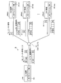
- FIG. 1 is a block diagram showing the configuration of the PON system.
- FIG. 2 is a sequence diagram showing a ranging processing procedure.
- FIG. 3 is a diagram for explaining a frame configuration and a packet configuration of an upstream signal from the ONT device to the OLT device.
- FIG. 4 is a diagram illustrating a sparsely mounted state in which a few ONT devices are operating among a plurality of ONT devices, and there are many non-operating ONT devices.
- FIG. 5A is a diagram illustrating a conventional packet configuration based on the number of branches.
- FIG. 5B is a diagram illustrating a packet configuration based on the number of branches in recent years.
- FIG. 6 is a block diagram illustrating a configuration of the OLT device.
- FIG. 1 is a block diagram showing the configuration of the PON system.
- FIG. 2 is a sequence diagram showing a ranging processing procedure.
- FIG. 3 is a diagram for explaining a frame configuration and a packet configuration of an
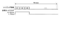
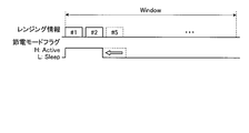
- FIG. 7 is a diagram illustrating an outline in which ranging information having a fixed periodicity is included in the delay measurement window.
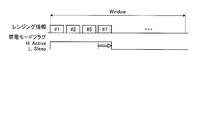
- FIG. 8 is a diagram illustrating an outline in which ranging information increases and the periodicity of the ranging information changes when end users dynamically increase.
- FIG. 9 is a diagram illustrating an outline in which ranging information decreases and the periodicity of ranging information changes when end users dynamically decrease.
- FIG. 10 is a diagram illustrating an overview in which the periodicity of the static power saving mode flag is impaired, and the ranging information and the state of the power saving mode flag are inconsistent.
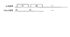
- FIG. 11 is a diagram illustrating an outline of a configuration example using a reset signal input from the MAC unit 102 to the optical transceiver unit 101.
- FIG. 12 is a diagram illustrating a configuration example in which the power is turned on / off using a timer unit having a reset signal and a timer function.
- FIG. 13 is a time chart when the timer unit turns off the power of the receiving unit.
- FIG. 14 is a block diagram illustrating the configuration of the OLT device according to the embodiment.
- FIG. 15 is a diagram illustrating a detailed configuration of the power saving mode flag generation unit.
- FIG. 16A is a diagram of a circuit example of the delay unit.
- FIG. 16B is a time chart illustrating signal states at respective points of the delay unit circuit.
- FIG. 17 is a diagram illustrating a circuit example of the latch circuit unit.
- FIG. 18 is a diagram illustrating an optical transceiver unit 101A including a packet monitoring unit.
- FIG. 19 is a diagram illustrating a circuit example of the signal disconnection detection unit.
- FIG. 20 is a diagram illustrating a circuit example of the PD / TIA unit.
- FIG. 21 is a diagram illustrating a circuit example of the LIM unit.
- FIG. 22 is a diagram illustrating a circuit example of the output unit.
- FIG. 23 is a diagram illustrating a detailed configuration of the power saving control unit.
- FIG. 24 is a block diagram illustrating a configuration of an OLT device according to an application example.
- FIG. 25 is a block diagram illustrating a detailed configuration of the light intensity detection unit according to the application example.
- FIG. 26 is a time chart illustrating the power saving control process according to the embodiment and the application example.
- FIG. 1 is a block diagram showing the configuration of the PON system.
- the OLT device 100 transmits a continuous signal in the ⁇ 1 band as a downstream signal to the ONT device 200ai via the star coupler SC.
- Each ONT device 200ai receives a continuous signal from the OLT device 100.
- each ONT device ai transmits a burst signal of ⁇ 2 band as an upstream signal to the OLT device 100 via the star coupler SC.
- Communication using a burst signal in the ⁇ 2 band varies in transmission distance and transmission path loss depending on the installation conditions of each ONT device 200ai. For this reason, the OLT device 100 performs time division multiplexing control so that burst signals output from the ONT devices 200ai do not collide with each other.
- optical communication is performed between the optical transceiver unit 101 of the OLT device 100 and the optical transceiver unit 201Ai of the ONT device 200ai.
- the optical transceiver unit 101 and the optical transceiver unit 201Ai are modules that are controlled by a MAC LSI (Media Access Control Large Scale Integration) and perform optical communication.
- MAC LSI Media Access Control Large Scale Integration
- a communication delay measurement is performed in order to communicate between the OLT and the ONT when a line is laid when an end user joins. It is carried out.
- the communication delay measurement is called “ranging” and is a function controlled by a MAC LSI generally mounted in the OLT apparatus 100.
- FIG. 2 is a sequence diagram showing a ranging processing procedure.
- the ONT device 200ai is activated.
- the ONT device 200ai transmits a frame signal to the OLT device 100 in order to achieve frame synchronization with the OLT device 100.
- step S13 the OLT device 100 that has received the frame signal from the ONT device 200ai transmits a registration request transmission permission signal to the OLT device 100 to the unregistered ONT device 200ai.
- step S ⁇ b> 14 the ONT device 200 ai transmits a registration request to the OLT device 100 so as to register itself with the OLT device 100.
- step S15 the OLT device 100 transmits the registration request transmission permission signal to the ONT device 200ai in step S13, and then receives the registration request from the ONT device 200ai in step S14.
- the distance between the devices 200ai is calculated.
- step S16 the OLT device 100 assigns an LL ID (Logical Link ID) to the ONT device 200ai that has transmitted the registration request received in step S14.
- the LL ID is an ID for uniquely identifying each ONT device 200ai in the PON system S.
- step S17 the OLT device 100 transmits a registration notification including the LL ID assigned in step S16 to the ONT device 200ai that has transmitted the registration request in step S14.
- step S18 the ONT device 200ai that has received the registration notification in step S17 transmits a registration notification confirmation indicating that the registration notification has been received to the OLT device 100.
- the OLT device 100 receives the registration notification confirmation, a series of registration processing of the ONT device 200ai is completed.
- FIG. 3 is a diagram for explaining a frame configuration and a packet configuration of an uplink signal from the ONT device 200ai to the OLT device 100.
- the frame of the uplink signal has a frame length with a transmission time of 1 [ms], for example.
- the frame of the uplink signal includes a data communication area for transmitting a packet from each end user and a ranging area used during ranging. Further, each packet having a packet length of 60 bytes included in the data communication area includes an overhead portion and a payload portion. Packets included in the data communication area are also referred to as PDS cells.
- the overhead part contains packet identification information, and the payload part contains user data.
- the overhead portion of 7 bytes in total includes “G”, “PR”, “DL”, and “DI” represented in FIG. “G” is a guard interval, which is a redundant part added for the purpose of preventing interference between packets.
- PR is a preamble, and includes a signal for causing the OLT device 100 to recognize the start of transmission of an upstream packet and giving timing for synchronization.
- DL is a delimiter and is information indicating the start position of the packet.
- DI is a data identifier and is identification information indicating the type of packet.
- the ranging area is, for example, a frame length with a transmission time of 1 [us].
- the ranging area includes one PDS-OAM (Operation Administration and Maintenance) packet called a delay measurement window for each ONT 200ai when there is a delay measurement instruction from the OLT device 100. Ranging is performed in this ranging area, and the time difference between the transmission timing of the registration request transmission permission signal transmitted from the OLT device 100 to each ONT device 200ai and the reception timing of the registration request that is a ranging packet from the ONT device 200ai is calculated. Measured as delay time.
- the ONT device 200ai can easily realize power saving by a combination of known technologies.
- the ONT devices 200ai are independent of each other, and in order to transmit a burst signal to the OLT device 100, a sleep mode (power saving mode) in which the circuit block is turned off except during transmission is obtained. It is easy to reduce power consumption.
- the OLT device 100 has a small number of ONT devices 200ai operating at the beginning of the service, and a small amount of data to be received. As shown in FIG. 4, this state is referred to as a sparsely mounted state in which a few ONT devices 200ai are operating among a plurality of ONT devices 200ai and a large number of inactive ONT devices 200ai exist.
- the number of branches by the star coupler SC is mainly 16 branches or 32 branches. For this reason, even if the sleep mode can be realized in the sparsely mounted state, the ratio of the sleep mode time to the delay measurement window in the ranging area is small. That is, even if the sleep mode time is secured, the number of delay measurement windows is small, so that the sleep mode time that can be secured in total is short. For this reason, when receiving a burst signal, the merit of shifting to the sleep mode is low.
- the packet transmission in the delay measurement window obtained from the ranging information from the MAC LSI is transmitted.
- a method of controlling the active mode (non-power saving mode) and the sleep mode of the OLT device 100 using the periodicity of the timing information is conceivable.
- FIG. 6 is a block diagram showing a configuration of the OLT device 100.
- the OLT device 100 includes an optical transceiver unit 101 and a MAC unit 102 that is a MAC LSI.
- the MAC unit 102 controls the PON system S.
- the MAC unit 102 recognizes a plurality of ONT devices 200ai, and performs packet transmission delay measurement when laying a line with each ONT device 200ai in order to communicate with the OLT device 100.
- Delay measurement is performed by a general function of the OLT device 100 called ranging as described above.
- packet transmission timing information (hereinafter also referred to as ranging information) from each ONT device 200ai can be obtained.
- the packet transmission timing information is information defining timing for transmitting a packet to the ONT device 200ai in consideration of a periodic delay time obtained by delay measurement.
- the optical transceiver unit 101 includes a power saving control unit 101a, a receiving unit 101b, and a packet information storage unit 101c.
- the packet information storage unit 101c acquires and stores periodic packet transmission timing information from the above-described packet transmission timing information. Then, a periodic power saving mode flag (a flag for identifying the active mode and the sleep mode) is generated from the stored transmission timing information, and is output to the power saving control unit 101a.
- the optical transceiver unit 101 acquires packet transmission timing information from the MAC unit 102 by low-speed serial communication of I2C (Inter-Integrated Circuit, SFP specification: 100 kbps).
- I2C Inter-Integrated Circuit, SFP specification: 100 kbps
- the power saving control unit 101a controls the power supply of the receiving unit 101b of the optical transceiver unit 101 in accordance with the periodic power saving mode flag input from the packet information storage unit 101c. Thereby, in the idling state where there is no reception packet and no transmission packet, the power of the reception unit 101b can be turned off to save power.
- the receiving unit 101b includes a PD (Photo Diode) / TIA (Trans Impedance amplifier) unit 101b1, a LIM (LIMiter amplifier) unit 101b2, and an output unit 101b3.
- the PD / TIA unit 101b1 converts a packet from an optical signal to an electrical signal by the photoelectric conversion element PD. Then, the PD / TIA unit 101b1 converts the electric signal from current to voltage by the current-voltage conversion element TIA and amplifies it.
- the PD / TIA unit 101b1 outputs the amplified voltage signal to the LIM unit 101b2.
- the LIM unit 101b2 removes over-input and amplification noise of the voltage signal input from the PD / TIA unit 101b1, and outputs it to the output unit 101b3.
- the output unit 101b3 demultiplexes a frame in which packets from a plurality of ONT devices 200ai are multiplexed into packets for each ONT device 200ai, and transmits each packet to, for example, an Ethernet (registered trademark) network.
- ranging information having a fixed periodicity is included in the delay measurement window.
- This ranging information is not changed once stored in the packet information storage unit 101c. Therefore, a power saving mode flag (H: active mode, L: sleep mode) having a fixed periodicity is generated based on the fixed ranging information. That is, as long as the ranging information is not changed, the power saving of the receiving unit 101b can be controlled by a static power saving mode flag having a fixed periodicity.
- H active mode
- L sleep mode
- the power saving mode flag also needs to be changed in periodicity. That is, when the number of ONT devices 200ai increases, it is necessary to extend the period in which the power saving mode flag becomes “H” by the increment (# 7 ranging information). Further, when the ONT device 200ai decreases, the cycle in which the power saving mode flag becomes “H” must be shortened by the decrease (# 5 ranging information).
- the periodicity of the ranging information is not changed because it is fixedly stored in the packet information storage unit 101c. That is, as shown in FIG. 10, the periodicity of the static power saving mode flag is impaired, and the ranging information and the state of the power saving mode flag become inconsistent.
- the ONT device 200ai is added, the corresponding ranging information is left-justified. For example, according to FIG. 8, when # 7 ranging information is added after # 5 ranging information, # 7 is set next to # 5 without leaving # 6 ranging information area.
- periodic packet transmission timing information is not stored in the optical transceiver unit 101, but packet transmission timing information from the MAC unit 102 is used directly, that is, ranging information is updated for each packet. It is possible. However, since the I2C communication method used between the MAC unit 102 and the optical transceiver unit 101 is low speed, it is impossible to follow the increase / decrease in the ranging information in real time.
- the MAC unit 102 inputs the optical transceiver unit 101 to the optical transceiver unit 101 for the purpose of initializing the ATC (Auto Threshold Control) of the optical transceiver unit 101 immediately before the packet is input. It is conceivable to use a reset signal. For example, as shown in FIG. 12, a configuration in which the power is turned on and off using a timer unit 101d having a reset signal and a timer function is conceivable.
- the frame is divided into a data area and a ranging area as shown in FIG. Since the data packet is input immediately after the reset in the data communication area, there is no problem even if the receiving unit 101b is turned off when there is no reset. However, in the ranging area, it is unclear at what timing the ranging packet is transmitted, and therefore the receiving unit 101b must always be turned on. In the configuration of the OLT device 100 shown in FIG. 12, the power may be turned off during ranging, and there is a possibility that packets during ranging cannot be detected.
- the timer unit 101d measures a predetermined time from the input of the reset signal, and when there is no new reset signal input within the predetermined time, the power saving control unit 101a Turn off the power.
- the transmission timing of the ranging packet is unknown in the ranging area. For this reason, as shown in FIG. 13, when the power of the receiving unit 101b is already turned off at the timing when the “#New” ranging packet is transmitted, there is a problem that the corresponding ranging packet may not be detected. .
- the technology disclosed in the following embodiments overcomes the background and problems described above, can follow the increase / decrease in real-time packets of the ONT device 200ai, and can be applied to the power saving applicable to the PON system S unique ranging. Allows control.
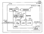
- FIG. 14 is a block diagram illustrating a configuration of the OLT device 100a according to the embodiment.
- the OLT device 100a includes an optical transceiver unit 101A and a MAC unit 102.
- the optical transceiver unit 101A includes a power saving control unit 101a, a receiving unit 101b, a power saving mode flag generating unit 101e, a packet monitoring unit 101f, and a pattern identifying unit 101g.
- the power saving control unit 101a performs power saving control of the receiving unit 101b of the OLT device 100a based on the power saving mode flag generated by the power saving mode flag generating unit 101e.
- the power saving mode flag generation unit 101e generates a power saving mode flag based on the packet transmission timing information obtained by the packet monitoring unit 101f and the reset signal output from the MAC unit 102.
- the packet monitoring unit 101f monitors packets transmitted from each ONT device 200ai.
- the pattern identification unit 101g identifies the packet in the data communication area and the packet in the ranging area, and outputs the identification result to the power saving mode flag generation unit 101e.
- the packet monitoring unit 101f monitors a packet transmitted from the ONT device 200ai, and includes a signal disconnection detection unit 101f1 as shown in FIG.
- the power saving mode flag generation unit 101e activates the power saving mode flag (non-power saving mode, power-on).
- the power saving mode flag generation unit 101e sets the power saving mode flag to sleep (power saving mode, power off) by the signal interruption detection signal obtained by the signal interruption detection unit 101f1 of the packet monitoring unit 101f.
- the power saving mode flag generation unit 101e activates the power saving mode flag and changes the sleep depending on the packet state in the packet data communication area, but always activates in the ranging area.
- the identification of the data communication area or the ranging area of the packet is performed by the pattern identification unit 101g.
- the pattern stored in a predetermined storage area not shown for reference is compared with the pattern of the packet in advance. Identify more.
- the power saving control unit 101a turns on / off the power of the receiving unit 101b based on the power saving mode flag.
- power saving is achieved by turning on / off the power of the receiving unit 101b of the optical transceiver unit 101A (not all circuit blocks but also some circuit blocks) according to the state of the packet. Is possible. Furthermore, during ranging, it is possible to perform ranging normally by always turning on the power of the receiving unit 101b regardless of the packet state.
- FIG. 15 is a diagram illustrating a detailed configuration of the power saving mode flag generation unit 101e.
- the power saving mode flag generation unit 101e includes a latch unit 101e1, an OR unit 101e2, a timer unit 101e3, a mask signal generation unit 101e4, and a delay unit 101e5.
- the latch unit 101e1 receives a reset signal from the MAC 102.
- the reset signal is one of control signals generally used in the OLT device 101a, and is a signal generated immediately before each packet based on ranging information for the purpose of threshold initialization of the optical transceiver unit 101A.
- the latch unit 101e1 has a function of detecting and latching (holding) a reset signal and resetting by a signal disconnection detection signal input from the delay unit 101e5.
- the latch unit 101e1 outputs a reset signal H (ON) or L (OFF) to the OR unit 101e2.
- the delay unit 101e5 delays the signal interruption detection signal obtained from the packet monitoring unit 101f until a predetermined condition is satisfied.
- the predetermined condition will be described later.
- the timer unit 101e3 receives a detection signal obtained by detecting the first packet signal in the data communication area within the delay measurement window identified by the pattern identification unit 101g, and receives a preset ranging area. Time.
- the timer unit 101e3 outputs a time measurement end signal to the mask signal generation unit 101e4 when the time measurement until receiving the preset ranging area is completed.
- the mask signal generation unit 101e4 generates a mask signal that is H (on) during ranging and L (off) otherwise, based on the timing end signal input from the timer unit 101e3. Then, the mask signal generation unit 101e4 outputs a mask signal to the OR unit 101e2.
- the OR unit 101e2 is a logic gate that calculates the logical sum of the reset signal input from the latch unit 101e1 and the mask signal input from the mask signal generation unit 101e4.
- the OR unit 101e2 outputs a logical sum of the reset signal and the mask signal to the power saving control unit 101a1 as a power saving mode flag.
- the signal output from the OR unit 101e2 is a power saving mode flag. In the data communication area, the power saving mode flag is changed to the active mode or the sleep mode depending on the packet state, but in the ranging area, the signal is always set to the active mode. Become.
- FIG. 16A is a diagram illustrating a circuit example of the delay unit 101e5.
- the delay unit 101e5 includes an inverting gate 101e5a, a resistor 101e5b, a diode 101e5c, a capacitor 101e5d, and an inverting gate 101e5e.
- the inverting gate 101e5a inverts the signal interruption detection signal input from the packet monitoring unit 101f and outputs the inverted signal to the resistor 101e5b.
- a grounded capacitor is connected to the signal output destination of the resistor 101e5b.
- a diode (commutator) 101e5c that inputs the signal output of the resistor 101e5b by looping back to the resistor 101e5b is connected.
- an inversion gate 101e5e that further inverts the signal output of the resistor 101e5b and outputs it to the latch unit 101e1 is connected.
- [Time chart of delay part] 16B is a time chart illustrating signal states at (A) to (D) of the circuit of the delay unit 101e5 illustrated in FIG.
- the amount of delay can be varied by adjusting the capacitor value of the capacitor 101e5d. Further, only the falling edge of the output signal is delayed, and the rising edge is not delayed.
- the delay time is preferably about guard time (25-30 ns for GPON).
- the signal in (A) is a signal loss detection signal.
- the signal in (B) is a signal obtained by inverting the signal break detection signal.
- the signal at the point (C) is a signal in which the voltage drop due to the resistor 101e5b is gradually canceled by the charging of the capacitor 101e5d and the edge gradually rises.
- the signal at the point (D) outputs an inverted signal of the signal at the point (C) only when the signal at the point (C) becomes H (ON). Therefore, the time until the signal at point (C) becomes H (ON) after the signal interruption detection signal is input is the delay time delayed by the delay unit 101e5.
- the above-described predetermined condition that defines the time for delaying the signal interruption detection signal obtained from the packet monitoring unit 101f is that the charging of the capacitor 101e5d is completed.
- FIG. 17 is a diagram illustrating a circuit example of the latch circuit unit 101e1.
- the latch circuit unit 101e1 detects and latches the input of the reset signal from the MAC unit 102, and resets the reset signal latch by the input of the output signal from the delay unit 105e.
- the latch circuit unit 101e1 includes an OR unit 101e1a, an OR unit 101e1b, and an AND unit 101e1c.
- the OR unit 101e1a outputs a logical sum having the input of the reset signal from the MAC unit 102 and the output signal from the delay unit 105e to the OR unit 101e1b and the AND unit 101e1c.
- the OR unit 101e1b outputs a logical sum having the outputs of the OR unit 101e1a and the AND unit 101e1c as inputs to the OR unit 101e2 of the power saving mode flag generation unit 101e and also outputs to the AND unit 101e1c.
- the AND unit 101e1c outputs a logical product having the outputs of the OR unit 101e1a and the OR unit 101e1b as inputs to the OR unit 101e1b.
- FIG. 18 is a diagram illustrating the optical transceiver unit 101A including the packet monitoring unit 101f.
- the packet monitoring unit 101f includes a signal disconnection detection unit 101f1.
- the signal disconnection detection unit 101f1 receives an input of a packet signal indicated by a voltage output from the PD / TIA unit 101b1 of the reception unit 101b. The presence or absence of packet signal input is detected and notified to the power saving mode flag generation unit 101e.
- FIG. 19 is a diagram illustrating a circuit example of the signal disconnection detection unit 101f1.
- the signal interruption detection unit 101f1 includes an AMP unit 101f1a that is a preamplifier that amplifies an input signal, a peak detection unit 101f1b that detects a peak of an output of the AMP unit 101f1a, and a bottom detection unit 101f1c that detects a bottom of an output of the AMP unit 101f1a.
- a threshold storage unit 101f1d that stores a voltage threshold for identifying H (ON) and L (OFF) of the signal, an output of the peak detection unit 101f1b and an output of the bottom detection unit 101f1c, and an output of the threshold storage unit 101f1d
- a CMP unit 101f1f that is a comparator that compares the output of the threshold value is included. Also included is an adding unit 101f1e that adds the output of the threshold value of the threshold storage unit 101f1d to the output of the bottom detection unit 101f1c.
- the CMP unit 101f1f outputs a signal with a packet when the output of the bottom detection unit 101f1c exceeds the threshold value. Further, the CMP unit 101f1f outputs a signal indicating no packet (signal disconnection detection signal) when the output of the peak detection unit 101f1v is below the threshold value.
- the output signal of the signal loss detection unit 101f1 may be an analog signal or a digital signal. Further, the output signal of the signal break detection unit 101f1 may be a serial signal or a parallel signal.
- the optical transceiver unit 101A includes a PD / TIA unit 101b1, a limiter amplifier LIM unit 101b2, and an output unit 101b3.
- FIG. 20 is a diagram illustrating a circuit example of the PD / TIA unit 101b1.
- the PD / TIA unit 101b1 is a photoelectric unit that receives an optical signal and converts it into an electrical signal.
- the TIA unit 101b amplifies the electrical signal converted by the PD unit 101b1a and converts the electrical signal into a voltage signal. including.
- FIG. 21 is a diagram illustrating a circuit example of the LIM unit 101b2.
- the LIM unit 101b2 includes a peak detection unit 101b2b that detects a peak of the electrical signal that is finally converted into a voltage signal by the PD / TIA unit 101b1, a bottom detection unit 101b2c that detects the bottom of the electrical signal, and a peak of the peak detection unit 101b2b.
- a resistor 101b2d for dropping the voltage of the output and a resistor 101b2e for dropping the voltage of the bottom output of the bottom detection unit 101b2c are included.
- the AMP unit is an amplifier that receives the voltage signal input by the PD / TIA unit 101b1, and the peak voltage signal and the bottom voltage signal that have been dropped by the resistor 101b2d and the resistor 101b2e, and amplifies and outputs both of them. 101b2a is included.
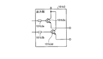
- FIG. 22 is a diagram illustrating a circuit example of the output unit 101b3.
- the output unit 101b3 includes a resistor 101b3a, a resistor 101b3b, a transistor 101b3c, and a transistor 101b3d.
- the transistor 101b3c uses a direct voltage signal output from the PD / TIA unit 101b1 and directly amplified by the LIM unit 101b2 as a base signal.
- the transistor 101b3d uses the peak voltage signal and the bottom voltage signal amplified by the LIM unit 101b2 as base signals.
- the collector terminals of the transistors 101b3c and 101b3d are connected to each other. As a result, if there is even a slight current difference between the direct voltage signal and the peak voltage signal and the bottom voltage signal, the direct voltage signal, the peak voltage signal, and the bottom voltage signal output a large current from each collector terminal. be able to.
- FIG. 23 is a diagram illustrating a detailed configuration of the power saving control unit 101a1.
- the power saving control unit 101a1 controls the power on / off of the receiving unit 101b based on the control signal (power saving mode flag) generated and output by the power saving mode flag generating unit 101e.
- the power saving control unit 101a1 includes a power supply unit 101a1a and a switch function unit 101a1b.
- the power supply unit 101a1a is a power supply that supplies power to the receiving unit 101b.
- the switch function unit 101a1b turns on / off the power supplied from the power supply unit 101a1a. Note that the power on / off target may be a specific functional block instead of the functional blocks of all receiving units.
- FIG. 24 is a block diagram illustrating a configuration of an OLT device 100a2 according to an application example of the disclosed technology.
- a light intensity detection unit 101h is provided as an alternative to the reset signal from the MAC unit 102 according to the embodiment.
- FIG. 25 is a block diagram illustrating a detailed configuration of a light intensity detection unit according to an application example of the disclosed technology.
- the light intensity detection unit 101h includes a current monitoring unit 101h1, a comparison unit 101h2, a pulse generation unit 101h3, and a threshold storage unit 101h4.
- the current monitor unit 101h1 detects an APD (Avalanche Photo Diode) current value.
- the APD current increases in current value according to the light intensity.
- the comparison unit 101h2 compares the APD current value with a preset threshold value stored in the threshold value storage unit 101h4. As a result of comparison, when the APD current value exceeds the threshold value, it is asserted (validated), and the pulse generated by the pulse generation unit 101h3 is output. The pulse becomes an input signal of the latch unit 101e1 in the power saving mode flag generation unit 101e.
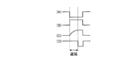
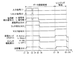
- FIG. 26 is a time chart illustrating the power saving control process according to the embodiment and the application example.
- the horizontal axis represents the time axis of one delay measurement frame.
- the delay measurement frame is divided into a data communication area and a ranging area.
- FIG. 26 (1) shows a packet signal transmitted from the ONT device 200ai to the OLT device 100.
- FIG. (2) indicates a reset signal (or APD current value). The reset signal is input immediately before each packet.
- (3) shows the output of the signal break detection unit 101f1. (3) is asserted (validated) when a preset threshold value for determining the presence or absence of a packet is exceeded based on the input signal of (1). Deassert (invalidate) when there is no packet signal.
- (6) indicates an output signal from the mask signal generation unit 101e4. Only the ranging area in the delay measurement frame is “H”, and the others are “L”. (7) shows the output signal of the power saving mode flag. This is the logical sum of the signals (5) and (6). (8) is a time chart of the output of the switch function unit 101a1b in the power saving control unit 101a1. The timing is the same as that of the power saving mode flag (7) and the signal.
- (9) indicates the power consumption of the OLT device 100a and the OLT device 100a2.
- the switch function unit 101a1b of (8) is switched off, the power of the block of the reception unit 101b is turned off, so that power consumption is reduced. That is, power consumption can be suppressed in the data communication area according to the presence or absence of a packet.
- the power saving mode flag is always “H”, the switch of the switch function unit 101a1b is always on.
- the power saving method that can follow the increase / decrease of the real-time packet accompanying the increase / decrease of the ONT device 200ai of the PON system and that can be applied at the time of ranging specific to the PON system is applied. It becomes possible. In addition, by reducing power consumption, it is possible to reduce the amount of heat generation and improve the integration degree of the OLT devices, that is, increase the number of ONT devices 200ai accommodated by the OLT device 100a and the OLT device 100a2. It becomes. That is, it becomes possible to control the power supplies of the circuit blocks of the OLT device 100a and the OLT device 100a2 in real time according to the state of the optical communication network.
- the present invention can be widely applied to an OLT device that is a main terminal device of a network.
- each component of each illustrated apparatus is functionally conceptual and does not necessarily need to be physically configured as illustrated.
- the specific form of distribution / integration of each device is not limited to that shown in the figure, and all or a part thereof may be functionally or physically distributed or arbitrarily distributed in arbitrary units according to various loads or usage conditions. Can be integrated and configured.
- Optical transceiver unit 101a 101a1 Power saving control unit 101a1a Power supply unit 101a1b Switch function unit 101b Receiver unit 101b1 PD / TIA unit 101b1a PD unit 101b2 LIM unit 101b2a AMP unit 101b2b Peak detection unit 101b2c Bottom detection unit 101b2d, 101b2e Resistance 101b3 Output unit 101b3a, 101b3b Resistance 101b3c, 101b3d Transistor 101c Packet information storage unit 101d Timer unit 101e Power saving mode flag generation unit 101e1 Latch unit 101e1 101e1b OR unit 101e1c AND unit 101e2 OR unit 101e3 Timer unit 101e4 Mask signal generation unit 101 e5 delay unit 101e5a, 101e5e inverting gate 101e5b resistor 101e5c diode 101e5d capacitor 101f packet monitoring unit 101f1 signal
Abstract
A packet monitoring unit (101f) monitors packets transmitted from an ONT device (200ai) and includes a signal-off detection unit (101f1). A power-saving mode flag generation unit (101e) activates a power-saving mode flag (non-power-saving mode, power supply input) when a reset signal is inputted from a MAC unit (102). The power-saving mode flag generation unit (101e) also sets the power-saving mode flag to a sleep state (power-saving mode, power supply cutoff) by using a signal-off detection signal obtained by the signal-off detection unit (101f1) in the packet monitoring unit (101f). The power-saving mode flag generation unit (101e) sets the power-saving mode flag to the active state or the sleep state depending on the packet state in a packet data communication region, but sets the power-saving mode flag always to the active state in a ranging region. A pattern discriminating unit (101g) discriminates between the packet data communication region and the ranging region.
Description
開示の技術は、光通信装置及び光通信装置の節電制御方法に関する。
The disclosed technology relates to an optical communication device and a power saving control method for the optical communication device.
光通信によるコンピュータ通信において、通信事業者(キャリア)の終端装置であるOLT(Optical Line Terminal)装置とエンドユーザ(通信事業加入者)の終端装置であるONT(Optical Network Terminal、ONU(Optical Network Unit)とも言う)装置を含む光ファイバ網の途中に一つの入力光を多数の出力に対して分岐させるスターカプラと呼ばれる分岐装置を挿入し、OLTからの一本の光ファイバを分岐させて複数のONTに接続するPON(Passive Optical Network)と呼ばれる通信システムがある。PONは、PDS(Passive Double Star)とも呼ばれる。
In computer communication using optical communication, the OLT (Optical Line Terminal) device, which is a terminal device for a carrier (carrier), and the ONT (Optical Network Terminal, ONU, which is a terminal device for an end user (communication business subscriber), are used. A branching device called a star coupler for branching one input light to many outputs in the middle of the optical fiber network including the device, and branching one optical fiber from the OLT to There is a communication system called PON (Passive Optical Network) that connects to ONT. PON is also called PDS (Passive Double Star).
終端装置を含む通信システムの従来技術として、例えば受信したパケットのヘッダ部分によって他の通信装置からの通信でなく自装置の電源のオン、オフの制御信号が入ったパケットであることを認識し、該制御信号によって自装置が受ける制御内容を認識する通信装置が提案されている。
As a prior art of a communication system including a termination device, for example, by recognizing that it is a packet containing a control signal for turning on / off the power of its own device instead of communication from another communication device by the header portion of the received packet, There has been proposed a communication device that recognizes the control contents received by the own device by the control signal.
また、他の従来技術として、主たる通信装置から、従たる通信装置の伝送速度に対応したパケットオーバヘッド部とフレーム同期を確立させるためのフレーム同期情報とを有するフレームパケット信号を一つのパケット信号長または一つのパケット時間長内に複数分割して配置してフレーム周期間隔で送信する通信システムが提案されている。
As another conventional technique, a frame packet signal having a packet overhead portion corresponding to the transmission speed of the slave communication device and frame synchronization information for establishing frame synchronization is transferred from the main communication device to one packet signal length or There has been proposed a communication system in which a packet is divided into a plurality of packet time lengths and transmitted at intervals of frame periods.
この従来技術では、従たる通信装置は、一つのパケット信号長または一つのパケット時間長内に複数分割されたフレームパケット信号から自装置の伝送速度に整合したフレームパケット信号を受信してフレーム同期情報を読み取ることによってフレーム同期を確立する。
In this prior art, the subordinate communication device receives a frame packet signal that matches the transmission rate of its own device from one packet signal length or a plurality of frame packet signals divided within one packet time length, and receives frame synchronization information. Establish frame synchronization by reading
一般的に、終端装置としての通信装置を含む通信網において、通信装置は、通信を行わないアイドル状態であっても通信に備えて常に電源を投入しておかねばならない。特に、上記OLT等の主たる通信装置は、上記ONT等の複数の従たる通信装置と同期を確立して通信を行わなければならないことから、消費電力が大きい。
Generally, in a communication network including a communication device as a termination device, the communication device must always be turned on in preparation for communication even in an idle state in which communication is not performed. In particular, the main communication device such as the OLT has a large power consumption because it must establish communication with a plurality of subordinate communication devices such as the ONT.
従って、省エネルギーの観点から、主たる通信装置の稼働中の消費電力を如何にして抑制するかが問題であった。しかしながら、上記の従来技術は、省エネルギーという観点がないため、通信装置の消費電力を抑制することが出来なかった。
Therefore, from the viewpoint of energy saving, there has been a problem of how to suppress the power consumption during operation of the main communication device. However, the above-described conventional technology has no viewpoint of energy saving, and thus cannot reduce the power consumption of the communication device.
開示の技術は、上記問題点(課題)を解消するためになされたものであって、省エネルギーの観点から、通信装置、特にOLT等の主たる通信装置の稼働中の消費電力を抑制する光通信装置及び光通信装置の節電制御方法を提供することを目的とする。
The disclosed technology has been made to solve the above problems (issues), and from the viewpoint of energy saving, an optical communication device that suppresses power consumption during operation of a communication device, particularly a main communication device such as an OLT. And it aims at providing the power-saving control method of an optical communication apparatus.
上述した問題を解決し、目的を達成するため、開示の技術は、複数の加入者側光通信装置に接続され、双方向の通信を行う光通信システムにおける事業者側の光通信装置において、加入者側光通信装置から送信されるパケットの有無を監視し、監視されるパケットの有無に基づき自装置の節電モードフラグを生成し、生成された節電モードフラグに基づき自装置の節電制御を行うことを要件とする。
In order to solve the above-described problems and achieve the object, the disclosed technique is applied to a subscriber-side optical communication apparatus in an optical communication system that is connected to a plurality of subscriber-side optical communication apparatuses and performs bidirectional communication. The presence / absence of a packet transmitted from the person side optical communication device is monitored, the power saving mode flag of the own device is generated based on the presence / absence of the monitored packet, and the power saving control of the own device is performed based on the generated power saving mode flag. Is a requirement.
開示の技術によれば、主たる終端装置と従たる終端装置との間のパケット送受信の遅延時間を計測する光通信システムの主たる終端装置において、遅延時間を計測する場合は主たる終端装置の電源を常にオンにし、遅延時間を計測する場合以外は、パケット送受信の有無に応じて主たる終端装置の電源のオン、オフを制御することが可能になる。よって、省電力化を図り、発熱量を削減し、主たる終端装置の集積度向上が可能となる。
According to the disclosed technology, in the main termination device of the optical communication system that measures the delay time of packet transmission / reception between the main termination device and the subordinate termination device, when measuring the delay time, the power supply of the main termination device is always turned on. Except when it is turned on and the delay time is measured, it is possible to control the power on / off of the main termination device according to the presence / absence of packet transmission / reception. Therefore, it is possible to save power, reduce the amount of heat generation, and improve the integration degree of the main termination device.
以下に添付図面を参照し、開示の技術の光通信装置及び光通信装置の節電制御方法に係る実施例を詳細に説明する。なお、以下の実施例は、PONシステムを例に説明する。しかし、PONシステムに限定されず、開示の技術的思想は、広く光通信システムに適用可能である。すなわち、以下の実施例によって開示の技術が限定されるものではない。実施例の説明に先立って、背景技術としてPONシステムの概要を説明する。
DETAILED DESCRIPTION Hereinafter, embodiments according to an optical communication device and a power saving control method of the optical communication device according to the disclosed technology will be described in detail with reference to the accompanying drawings. In the following embodiments, a PON system will be described as an example. However, the technical idea disclosed is not limited to the PON system, and can be widely applied to the optical communication system. In other words, the disclosed technology is not limited by the following embodiments. Prior to the description of the embodiments, an outline of a PON system will be described as background art.
[PONシステムの概要]
図1は、PONシステムの構成を示すブロック図である。同図に示すように、PONシステムSは、通信事業者の終端装置である一台のOLT装置100と、ユーザの終端装置である複数のONT装置200ai(i=1、2、・・・、n)とがスターカプラSCを介して双方向通信を行うように接続されている。OLT装置100は、スターカプラSCを介してONT装置200aiへ、下り信号としてλ1帯の連続信号を送信する。各ONT装置200aiは、OLT装置100からの連続信号を受信する。 [Outline of PON system]
FIG. 1 is a block diagram showing the configuration of the PON system. As shown in the figure, the PON system S includes oneOLT device 100 that is a communication device termination device and a plurality of ONT devices 200ai (i = 1, 2,...) That are user termination devices. n) is connected to perform bidirectional communication via the star coupler SC. The OLT device 100 transmits a continuous signal in the λ1 band as a downstream signal to the ONT device 200ai via the star coupler SC. Each ONT device 200ai receives a continuous signal from the OLT device 100.
図1は、PONシステムの構成を示すブロック図である。同図に示すように、PONシステムSは、通信事業者の終端装置である一台のOLT装置100と、ユーザの終端装置である複数のONT装置200ai(i=1、2、・・・、n)とがスターカプラSCを介して双方向通信を行うように接続されている。OLT装置100は、スターカプラSCを介してONT装置200aiへ、下り信号としてλ1帯の連続信号を送信する。各ONT装置200aiは、OLT装置100からの連続信号を受信する。 [Outline of PON system]
FIG. 1 is a block diagram showing the configuration of the PON system. As shown in the figure, the PON system S includes one
また、各ONT装置aiは、スターカプラSCを介してOLT装置100へ、上り信号としてλ2帯のバースト信号を送信する。λ2帯のバースト信号による通信は、各ONT装置200aiの設置条件により、伝送距離や伝送路の損失にバラツキがある。このため、OLT装置100は、各ONT装置200aiから出力されるバースト信号同士がぶつからないよう時分割多重制御を行っている。
In addition, each ONT device ai transmits a burst signal of λ2 band as an upstream signal to the OLT device 100 via the star coupler SC. Communication using a burst signal in the λ2 band varies in transmission distance and transmission path loss depending on the installation conditions of each ONT device 200ai. For this reason, the OLT device 100 performs time division multiplexing control so that burst signals output from the ONT devices 200ai do not collide with each other.
なお、図1に示すように、OLT装置100の光トランシーバ部101と、ONT装置200aiの光トランシーバ部201Aiとの間で光通信を行う。光トランシーバ部101及び光トランシーバ部201Aiは、MAC LSI(Media Access Control Large Scale Integration)によって制御され光通信を行うモジュールである。
As shown in FIG. 1, optical communication is performed between the optical transceiver unit 101 of the OLT device 100 and the optical transceiver unit 201Ai of the ONT device 200ai. The optical transceiver unit 101 and the optical transceiver unit 201Ai are modules that are controlled by a MAC LSI (Media Access Control Large Scale Integration) and perform optical communication.
また、PONシステムSは、接続された複数の各ONT装置200aiまでの伝送距離が異なることから、エンドユーザ加入時に伴う回線敷設の際、OLTとONTとの間で通信するために通信の遅延測定を行っている。通信の遅延測定は、「レンジング」と呼ばれ、OLT装置100に一般的に搭載されているMAC LSIによって制御される機能である。
In addition, since the PON system S has different transmission distances to each of a plurality of connected ONT devices 200ai, a communication delay measurement is performed in order to communicate between the OLT and the ONT when a line is laid when an end user joins. It is carried out. The communication delay measurement is called “ranging” and is a function controlled by a MAC LSI generally mounted in the OLT apparatus 100.
[レンジング処理の概要]
図2は、レンジングの処理手順を示すシーケンス図である。先ず、ステップS11で、ONT装置200aiが起動される。そして、ステップS12では、ONT装置200aiは、OLT装置100とフレーム同期を取るために、OLT装置100に対してフレーム信号を送信する。 [Overview of the ranging process]
FIG. 2 is a sequence diagram showing a ranging processing procedure. First, in step S11, the ONT device 200ai is activated. In step S12, the ONT device 200ai transmits a frame signal to theOLT device 100 in order to achieve frame synchronization with the OLT device 100.
図2は、レンジングの処理手順を示すシーケンス図である。先ず、ステップS11で、ONT装置200aiが起動される。そして、ステップS12では、ONT装置200aiは、OLT装置100とフレーム同期を取るために、OLT装置100に対してフレーム信号を送信する。 [Overview of the ranging process]
FIG. 2 is a sequence diagram showing a ranging processing procedure. First, in step S11, the ONT device 200ai is activated. In step S12, the ONT device 200ai transmits a frame signal to the
ステップS13では、ONT装置200aiからフレーム信号を受信したOLT装置100は、未登録のONT装置200aiに対してOLT装置100へ登録要求の送信許可信号を送信する。ステップS14では、ONT装置200aiは、OLT装置100に対して自装置をOLT装置100に登録するよう登録要求を送信する。
In step S13, the OLT device 100 that has received the frame signal from the ONT device 200ai transmits a registration request transmission permission signal to the OLT device 100 to the unregistered ONT device 200ai. In step S <b> 14, the ONT device 200 ai transmits a registration request to the OLT device 100 so as to register itself with the OLT device 100.
ステップS15では、OLT装置100は、ステップS13でONT装置200aiへ登録要求の送信許可信号を送信してからステップS14でONT装置200aiから登録要求を受信するまでの時間に基づき、OLT装置100及びONT装置200ai間の距離を算出する。
In step S15, the OLT device 100 transmits the registration request transmission permission signal to the ONT device 200ai in step S13, and then receives the registration request from the ONT device 200ai in step S14. The distance between the devices 200ai is calculated.
ステップS16では、OLT装置100は、ステップS14で受信した登録要求を送信したONT装置200aiへLL ID(Logical Link ID)を付与する。LL IDは、PONシステムS内で各ONT装置200aiを一意に識別するIDである。
In step S16, the OLT device 100 assigns an LL ID (Logical Link ID) to the ONT device 200ai that has transmitted the registration request received in step S14. The LL ID is an ID for uniquely identifying each ONT device 200ai in the PON system S.
ステップS17では、OLT装置100は、ステップS14で登録要求を送信してきたONT装置200aiに対してステップS16で付与したLL IDを含む登録通知を送信する。ステップS18では、ステップS17の登録通知を受信したONT装置200aiは、OLT装置100に対して登録通知を受信したことを示す登録通知確認を送信する。OLT装置100が登録通知確認を受信することによって、一連のONT装置200aiの登録処理は終了する。
In step S17, the OLT device 100 transmits a registration notification including the LL ID assigned in step S16 to the ONT device 200ai that has transmitted the registration request in step S14. In step S18, the ONT device 200ai that has received the registration notification in step S17 transmits a registration notification confirmation indicating that the registration notification has been received to the OLT device 100. When the OLT device 100 receives the registration notification confirmation, a series of registration processing of the ONT device 200ai is completed.
[上り信号のフレーム構成及びパケット構成]
図3は、ONT装置200aiからOLT装置100への上り信号のフレーム構成及びパケット構成を説明する図である。上り信号のフレームは、例えば1[ms]の伝送時間のフレーム長である。上り信号のフレームは、各エンドユーザからのパケットを送信するデータ通信領域と、レンジング時に使用されるレンジング領域とを含む。さらに、データ通信領域に含まれるパケット長60バイトの各パケットは、オーバーヘッド部と、ペイロード部とを含む。データ通信領域に含まれるパケットは、PDSセルとも呼ばれる。 [Frame structure and packet structure of uplink signal]
FIG. 3 is a diagram for explaining a frame configuration and a packet configuration of an uplink signal from the ONT device 200ai to theOLT device 100. The frame of the uplink signal has a frame length with a transmission time of 1 [ms], for example. The frame of the uplink signal includes a data communication area for transmitting a packet from each end user and a ranging area used during ranging. Further, each packet having a packet length of 60 bytes included in the data communication area includes an overhead portion and a payload portion. Packets included in the data communication area are also referred to as PDS cells.
図3は、ONT装置200aiからOLT装置100への上り信号のフレーム構成及びパケット構成を説明する図である。上り信号のフレームは、例えば1[ms]の伝送時間のフレーム長である。上り信号のフレームは、各エンドユーザからのパケットを送信するデータ通信領域と、レンジング時に使用されるレンジング領域とを含む。さらに、データ通信領域に含まれるパケット長60バイトの各パケットは、オーバーヘッド部と、ペイロード部とを含む。データ通信領域に含まれるパケットは、PDSセルとも呼ばれる。 [Frame structure and packet structure of uplink signal]
FIG. 3 is a diagram for explaining a frame configuration and a packet configuration of an uplink signal from the ONT device 200ai to the
オーバーヘッド部はパケットの識別情報、ペイロード部はユーザデータを含む。合計7バイトのオーバーヘッド部は、図3で表記される「G」、「PR」、「DL」、「DI」を含む。「G」はガードインターバルであり、パケット同士の干渉を防ぐ目的で付加される冗長部である。「PR」はプリアンブルであり、OLT装置100に上りパケットの送信開始を認識させ、同期をとるタイミングを与えるための信号を含む。「DL」はデリミタであり、パケットの開始位置を示す情報である。「DI」はデータ・アイデンティフアィアであり、パケットの種別を示す識別情報である。
The overhead part contains packet identification information, and the payload part contains user data. The overhead portion of 7 bytes in total includes “G”, “PR”, “DL”, and “DI” represented in FIG. “G” is a guard interval, which is a redundant part added for the purpose of preventing interference between packets. “PR” is a preamble, and includes a signal for causing the OLT device 100 to recognize the start of transmission of an upstream packet and giving timing for synchronization. “DL” is a delimiter and is information indicating the start position of the packet. “DI” is a data identifier and is identification information indicating the type of packet.
レンジング領域は、例えば1[us]の伝送時間のフレーム長である。レンジング領域は、OLT装置100から遅延測定指示があった場合、ONT200ai毎の遅延測定ウィンドウと呼ばれるPDS-OAM(Operation Administration and Maintenance)パケットを一つ含む。レンジングはこのレンジング領域で行われ、OLT装置100から各ONT装置200aiへ送信される登録要求送信許可信号の送信タイミングと、ONT装置200aiからのレンジング用パケットである登録要求の受信タイミングとの時間差を遅延時間として測定する。
The ranging area is, for example, a frame length with a transmission time of 1 [us]. The ranging area includes one PDS-OAM (Operation Administration and Maintenance) packet called a delay measurement window for each ONT 200ai when there is a delay measurement instruction from the OLT device 100. Ranging is performed in this ranging area, and the time difference between the transmission timing of the registration request transmission permission signal transmitted from the OLT device 100 to each ONT device 200ai and the reception timing of the registration request that is a ranging packet from the ONT device 200ai is calculated. Measured as delay time.
[PONシステムにおける省電力化]
ところで、PONシステムSにおいて、OLT装置100は、膨大なエンドユーザを収容することから、システム全体で消費する電力は極めて大きい。このため、PONシステムSを始めとする光アクセスシステムにおいて省電力化が要求されている。省電力化にあたり、システムの機能維持との両立が課題となる。 [Power saving in PON system]
By the way, in the PON system S, since theOLT apparatus 100 accommodates a huge number of end users, the power consumed by the entire system is extremely large. For this reason, power saving is required in optical access systems such as the PON system S. In order to save power, it is important to maintain system functions.
ところで、PONシステムSにおいて、OLT装置100は、膨大なエンドユーザを収容することから、システム全体で消費する電力は極めて大きい。このため、PONシステムSを始めとする光アクセスシステムにおいて省電力化が要求されている。省電力化にあたり、システムの機能維持との両立が課題となる。 [Power saving in PON system]
By the way, in the PON system S, since the
ONT装置200aiは、周知技術の組み合わせで省電力化が実現容易である。PONシステムSにおいてONT装置200aiは各々独立しており、かつ、OLT装置100へバースト信号を送信するため、送信時以外は回路ブロックをオフにするスリープ・モード(省電力モード)とすることにより、消費電力を抑えることが容易である。
The ONT device 200ai can easily realize power saving by a combination of known technologies. In the PON system S, the ONT devices 200ai are independent of each other, and in order to transmit a burst signal to the OLT device 100, a sleep mode (power saving mode) in which the circuit block is turned off except during transmission is obtained. It is easy to reduce power consumption.
これに対し、OLT装置100は、サービス開始当初は稼動しているONT装置200aiが少なく、受信するデータ量も少ない。この状態は、図4に示すとおり、複数のONT装置200aiのうち稼働しているONT装置200aiが少なく、未稼働のONT装置200aiが多数存在する疎実装状態という。
On the other hand, the OLT device 100 has a small number of ONT devices 200ai operating at the beginning of the service, and a small amount of data to be received. As shown in FIG. 4, this state is referred to as a sparsely mounted state in which a few ONT devices 200ai are operating among a plurality of ONT devices 200ai and a large number of inactive ONT devices 200ai exist.
疎実装状態の場合、前述のMAC LSIからのレンジング情報を用いて、OLT装置100の電源をオフにして容易に省電力化を図ることができる。しかし、図5-1に示すとおり、従来は、スターカプラSCによる分岐数は、16分岐又は32分岐が主流であった。このため、疎実装状態においてスリープ・モードが実現できたとしても、レンジング領域の遅延測定ウィンドウに対するスリープ・モードの時間の比率が小さい。すなわち、スリープ・モードの時間を確保したとしても、遅延測定ウィンドウの数が少ないため、トータルで確保できるスリープ・モードの時間が短い。このため、バースト信号を受信する際、スリープ・モードへ移行するメリットが低かった。
In the sparsely mounted state, it is possible to easily save power by turning off the power of the OLT device 100 using the ranging information from the MAC LSI described above. However, as shown in FIG. 5-1, conventionally, the number of branches by the star coupler SC is mainly 16 branches or 32 branches. For this reason, even if the sleep mode can be realized in the sparsely mounted state, the ratio of the sleep mode time to the delay measurement window in the ranging area is small. That is, even if the sleep mode time is secured, the number of delay measurement windows is small, so that the sleep mode time that can be secured in total is short. For this reason, when receiving a burst signal, the merit of shifting to the sleep mode is low.
しかし、近年、ITUT-984.2 ClassC/C+に基づき、スターカプラSCによる分岐数を増やすことが可能となった。図5-2に示すように、分岐数が多ければ、レンジング領域の遅延測定ウィンドウの数が多くなり、トータルで確保できるスリープ・モードの時間が長くなる。このため、OLT装置100のアイドリング時の省電力化のメリットが期待されるようになってきた。
However, in recent years, it has become possible to increase the number of branches by the star coupler SC, based on ITUT-984.2 Class C / C +. As shown in FIG. 5B, if the number of branches is large, the number of delay measurement windows in the ranging area increases, and the sleep mode time that can be secured in total increases. For this reason, the merit of the power saving at the time of idling of the OLT apparatus 100 has come to be expected.
そこで、例えば疎実装状態でのOLT装置100の省電力を化行う場合、疎実装状態での省電力化を実現する方法として、MAC LSIからのレンジング情報により得られた遅延測定ウィンドウ内のパケット送出タイミング情報の周期性を用いてOLT装置100のアクティブ・モード(非省電力モード)及びスリープ・モードを制御する方法が考えられる。
Therefore, for example, when the power saving of the OLT device 100 in the sparsely mounted state is performed, as a method for realizing the power saving in the sparsely mounted state, the packet transmission in the delay measurement window obtained from the ranging information from the MAC LSI is transmitted. A method of controlling the active mode (non-power saving mode) and the sleep mode of the OLT device 100 using the periodicity of the timing information is conceivable.
[OLT装置の構成]
図6は、OLT装置100の構成を示すブロック図である。OLT装置100は、光トランシーバ部101と、MAC LSIであるMAC部102とを含む。MAC部102は、PONシステムSを制御する。MAC部102は、例えば複数のONT装置200aiを認識し、OLT装置100との間で通信するために各ONT装置200aiとの回線敷設時にパケット送信の遅延測定を行う。 [Configuration of OLT device]
FIG. 6 is a block diagram showing a configuration of theOLT device 100. The OLT device 100 includes an optical transceiver unit 101 and a MAC unit 102 that is a MAC LSI. The MAC unit 102 controls the PON system S. For example, the MAC unit 102 recognizes a plurality of ONT devices 200ai, and performs packet transmission delay measurement when laying a line with each ONT device 200ai in order to communicate with the OLT device 100.
図6は、OLT装置100の構成を示すブロック図である。OLT装置100は、光トランシーバ部101と、MAC LSIであるMAC部102とを含む。MAC部102は、PONシステムSを制御する。MAC部102は、例えば複数のONT装置200aiを認識し、OLT装置100との間で通信するために各ONT装置200aiとの回線敷設時にパケット送信の遅延測定を行う。 [Configuration of OLT device]
FIG. 6 is a block diagram showing a configuration of the
遅延測定は、上述したように、レンジングと呼ばれるOLT装置100の一般的な機能により行われる。遅延測定によって、各ONT装置200aiからのパケット送出タイミング情報(以下、レンジング情報と呼ぶ場合がある)を得ることができる。パケット送出タイミング情報とは、遅延測定によって得られた周期的な遅延時間を考慮してONT装置200aiへパケットを送信するタイミングを規定する情報である。
Delay measurement is performed by a general function of the OLT device 100 called ranging as described above. Through the delay measurement, packet transmission timing information (hereinafter also referred to as ranging information) from each ONT device 200ai can be obtained. The packet transmission timing information is information defining timing for transmitting a packet to the ONT device 200ai in consideration of a periodic delay time obtained by delay measurement.
光トランシーバ部101は、節電制御部101aと、受信部101bと、パケット情報記憶部101cとを含む。パケット情報記憶部101cは、前述のパケット送出タイミング情報から周期的なパケット送信タイミング情報を取得して記憶する。そして、記憶した送出タイミング情報から周期的な節電モードフラグ(アクティブ・モード及びスリープ・モードを識別するフラグ)を生成して節電制御部101aへ出力する。なお、光トランシーバ部101は、MAC部102からI2C(Inter-Integrated Circuit、SFP仕様:100kbps)の低速なシリアル通信によりパケット送信タイミング情報を取得する。
The optical transceiver unit 101 includes a power saving control unit 101a, a receiving unit 101b, and a packet information storage unit 101c. The packet information storage unit 101c acquires and stores periodic packet transmission timing information from the above-described packet transmission timing information. Then, a periodic power saving mode flag (a flag for identifying the active mode and the sleep mode) is generated from the stored transmission timing information, and is output to the power saving control unit 101a. The optical transceiver unit 101 acquires packet transmission timing information from the MAC unit 102 by low-speed serial communication of I2C (Inter-Integrated Circuit, SFP specification: 100 kbps).
節電制御部101aは、パケット情報記憶部101cから入力された周期的な節電モードフラグに従い、光トランシーバ部101の受信部101bの電源を制御する。これにより、受信パケット及び送信パケットが無いアイドリング状態の際、受信部101bの電源をオフにし、省電力化を図ることができる。
The power saving control unit 101a controls the power supply of the receiving unit 101b of the optical transceiver unit 101 in accordance with the periodic power saving mode flag input from the packet information storage unit 101c. Thereby, in the idling state where there is no reception packet and no transmission packet, the power of the reception unit 101b can be turned off to save power.
なお、受信部101bは、PD(Photo Diode)/TIA(Trans Impedance amplifier)部101b1、LIM(LIMiter amplifier)部101b2、出力部101b3を含む。PD/TIA部101b1は、光電変換素子PDによってパケットを光信号から電気信号へ変換する。そして、PD/TIA部101b1は、電流電圧変換素子TIAによって電気信号を電流から電圧へ変換して増幅する。PD/TIA部101b1は、増幅した電圧信号をLIM部101b2へ出力する。
The receiving unit 101b includes a PD (Photo Diode) / TIA (Trans Impedance amplifier) unit 101b1, a LIM (LIMiter amplifier) unit 101b2, and an output unit 101b3. The PD / TIA unit 101b1 converts a packet from an optical signal to an electrical signal by the photoelectric conversion element PD. Then, the PD / TIA unit 101b1 converts the electric signal from current to voltage by the current-voltage conversion element TIA and amplifies it. The PD / TIA unit 101b1 outputs the amplified voltage signal to the LIM unit 101b2.
LIM部101b2は、PD/TIA部101b1から入力された電圧信号の過入力及び増幅ノイズを除去して出力部101b3へ出力する。出力部101b3は、複数のONT装置200aiからのパケットが多重されたフレームからONT装置200ai毎のパケットへと多重を解除し、例えばイーサネット(登録商標)網へ各パケットを送出する。
The LIM unit 101b2 removes over-input and amplification noise of the voltage signal input from the PD / TIA unit 101b1, and outputs it to the output unit 101b3. The output unit 101b3 demultiplexes a frame in which packets from a plurality of ONT devices 200ai are multiplexed into packets for each ONT device 200ai, and transmits each packet to, for example, an Ethernet (registered trademark) network.
上記のようにOLT装置100を構成した場合、図7に示す様に、遅延測定ウィンドウ内に固定的な周期性を持つレンジング情報が含まれる。このレンジング情報は、一度パケット情報記憶部101cに記憶されると変更されることはない。従って、固定的なレンジング情報に基づき固定的な周期性を持つ節電モードフラグ(H:アクティブ・モード、L:スリープ・モード)が生成される。すなわち、レンジング情報に変更がない限り、固定的な周期性を持つ静的な節電モードフラグによって受信部101bの省電力化が制御可能になる。
When the OLT apparatus 100 is configured as described above, as shown in FIG. 7, ranging information having a fixed periodicity is included in the delay measurement window. This ranging information is not changed once stored in the packet information storage unit 101c. Therefore, a power saving mode flag (H: active mode, L: sleep mode) having a fixed periodicity is generated based on the fixed ranging information. That is, as long as the ranging information is not changed, the power saving of the receiving unit 101b can be controlled by a static power saving mode flag having a fixed periodicity.
[上記構成の問題点]
しかしながら、上記OLT装置100の構成では、エンドユーザが動的に増減する場合、レンジング情報が増加又は減少し、レンジング情報の周期性が変わる。これに応じて、図8及び図9に示すように、節電モードフラグも周期性の変更が必要である。すなわち、ONT装置200aiが増加した場合、増加分(#7のレンジング情報)だけ節電モードフラグが「H」となる周期を延長しなければならない。また、ONT装置200aiが減少した場合、減少分(#5のレンジング情報)だけ節電モードフラグが「H」となる周期を短縮しなければならない。 [Problems of the above configuration]
However, in the configuration of theOLT device 100, when the end user dynamically increases or decreases, the ranging information increases or decreases, and the periodicity of the ranging information changes. Accordingly, as shown in FIGS. 8 and 9, the power saving mode flag also needs to be changed in periodicity. That is, when the number of ONT devices 200ai increases, it is necessary to extend the period in which the power saving mode flag becomes “H” by the increment (# 7 ranging information). Further, when the ONT device 200ai decreases, the cycle in which the power saving mode flag becomes “H” must be shortened by the decrease (# 5 ranging information).
しかしながら、上記OLT装置100の構成では、エンドユーザが動的に増減する場合、レンジング情報が増加又は減少し、レンジング情報の周期性が変わる。これに応じて、図8及び図9に示すように、節電モードフラグも周期性の変更が必要である。すなわち、ONT装置200aiが増加した場合、増加分(#7のレンジング情報)だけ節電モードフラグが「H」となる周期を延長しなければならない。また、ONT装置200aiが減少した場合、減少分(#5のレンジング情報)だけ節電モードフラグが「H」となる周期を短縮しなければならない。 [Problems of the above configuration]
However, in the configuration of the
しかし、レンジング情報の周期性は、固定的にパケット情報記憶部101cに記憶されているため変更されない。すなわち、図10に示すように、静的な節電モードフラグの周期性が損なわれてしまい、レンジング情報と節電モードフラグの状態とが不整合となってしまう。一般的にONT装置200aiが追加された場合、対応するレンジング情報は先詰めされる。例えば図8によると、#5のレンジング情報の後に#7のレンジング情報が追加された場合、#6のレンジング情報の領域を空けず#5の次に#7がセットされる。
However, the periodicity of the ranging information is not changed because it is fixedly stored in the packet information storage unit 101c. That is, as shown in FIG. 10, the periodicity of the static power saving mode flag is impaired, and the ranging information and the state of the power saving mode flag become inconsistent. Generally, when the ONT device 200ai is added, the corresponding ranging information is left-justified. For example, according to FIG. 8, when # 7 ranging information is added after # 5 ranging information, # 7 is set next to # 5 without leaving # 6 ranging information area.
上記問題を解決するため、例えば周期的なパケット送出タイミング情報を光トランシーバ部101内に記憶せず、MAC部102からのパケット送出タイミング情報を直接使用する、すなわち、パケット毎にレンジング情報を更新することが考えられる。しかし、MAC部102及び光トランシーバ部101の間で用いられるI2Cの通信方式は低速であるため、リアルタイムにレンジング情報の増減に追随することは不可能である。
In order to solve the above problem, for example, periodic packet transmission timing information is not stored in the optical transceiver unit 101, but packet transmission timing information from the MAC unit 102 is used directly, that is, ranging information is updated for each packet. It is possible. However, since the I2C communication method used between the MAC unit 102 and the optical transceiver unit 101 is low speed, it is impossible to follow the increase / decrease in the ranging information in real time.
また、上記問題を解決するため、図11に示すような、パケットが入力する直前に光トランシーバ部101のATC(Auto Threshold Control)の初期化等を目的としてMAC部102から光トランシーバ部101へ入力されるリセット信号を用いることが考えられる。例えば図12に示すように、リセット信号及びタイマー機能を有するタイマー部101dを用いて電源をオンオフする構成が考えられる。
In order to solve the above problem, as shown in FIG. 11, the MAC unit 102 inputs the optical transceiver unit 101 to the optical transceiver unit 101 for the purpose of initializing the ATC (Auto Threshold Control) of the optical transceiver unit 101 immediately before the packet is input. It is conceivable to use a reset signal. For example, as shown in FIG. 12, a configuration in which the power is turned on and off using a timer unit 101d having a reset signal and a timer function is conceivable.
しかし、上述したように、フレームは図3に示すようなデータ領域とレンジング領域に分かれている。データ通信領域はリセット直後にデータパケットが入力されるため、リセットがないときは受信部101bを電源オフにしても問題ない。しかし、レンジング領域では、いかなるタイミングでレンジング用パケットが送出されるか不明であるため、常に受信部101bを電源オンにしなければならない。図12に示すOLT装置100の構成では、レンジング中に電源がオフになってしまう場合があり、レンジング時のパケットを検出できない可能性がある。
However, as described above, the frame is divided into a data area and a ranging area as shown in FIG. Since the data packet is input immediately after the reset in the data communication area, there is no problem even if the receiving unit 101b is turned off when there is no reset. However, in the ranging area, it is unclear at what timing the ranging packet is transmitted, and therefore the receiving unit 101b must always be turned on. In the configuration of the OLT device 100 shown in FIG. 12, the power may be turned off during ranging, and there is a possibility that packets during ranging cannot be detected.
すなわち、図13のタイムチャートに示すように、タイマー部101dは、リセット信号の入力から所定時間を計時し、所定時間内に新たなリセット信号の入力がない場合、節電制御部101aが受信部101bの電源をオフにする。前述の通り、レンジング領域ではレンジングパケットの送出タイミングが不明である。このため、図13に示すように「#New」のレンジングパケットが送出されたタイミングでは既に受信部101bの電源がオフにされている場合、該当レンジングパケットは検出されない可能性があるという不都合が生じる。
That is, as shown in the time chart of FIG. 13, the timer unit 101d measures a predetermined time from the input of the reset signal, and when there is no new reset signal input within the predetermined time, the power saving control unit 101a Turn off the power. As described above, the transmission timing of the ranging packet is unknown in the ranging area. For this reason, as shown in FIG. 13, when the power of the receiving unit 101b is already turned off at the timing when the “#New” ranging packet is transmitted, there is a problem that the corresponding ranging packet may not be detected. .
以下の実施例で開示の技術は、上記背景及び問題点を克服し、ONT装置200aiのリアルタイムなパケットの増減に追随することができ、かつ、PONシステムS特有のレンジング時にも適用可能な省電力制御を可能とする。
The technology disclosed in the following embodiments overcomes the background and problems described above, can follow the increase / decrease in real-time packets of the ONT device 200ai, and can be applied to the power saving applicable to the PON system S unique ranging. Allows control.
以下に開示の技術に係る実施例を詳細に説明する。以下では、光通信システムはPONシステムSを例にして説明する。なお、上記背景及び問題点で説明した機能ブロックと同一符号が付与されている機能ブロックの説明は省略する。
Examples according to the disclosed technology will be described in detail below. Hereinafter, the optical communication system will be described using the PON system S as an example. In addition, description of the functional block to which the same code | symbol as the functional block demonstrated in the said background and a problem is provided is abbreviate | omitted.
[実施例に係るOLT装置の構成]
図14は、実施例に係るOLT装置100aの構成を示すブロック図である。OLT装置100aは、光トランシーバ部101Aと、MAC部102とを含む。光トランシーバ部101Aは、節電制御部101a、受信部101b、節電モードフラグ生成部101e、パケット監視部101f、パターン識別部101gを含む。 [Configuration of OLT Device According to Embodiment]
FIG. 14 is a block diagram illustrating a configuration of theOLT device 100a according to the embodiment. The OLT device 100a includes an optical transceiver unit 101A and a MAC unit 102. The optical transceiver unit 101A includes a power saving control unit 101a, a receiving unit 101b, a power saving mode flag generating unit 101e, a packet monitoring unit 101f, and a pattern identifying unit 101g.
図14は、実施例に係るOLT装置100aの構成を示すブロック図である。OLT装置100aは、光トランシーバ部101Aと、MAC部102とを含む。光トランシーバ部101Aは、節電制御部101a、受信部101b、節電モードフラグ生成部101e、パケット監視部101f、パターン識別部101gを含む。 [Configuration of OLT Device According to Embodiment]
FIG. 14 is a block diagram illustrating a configuration of the
節電制御部101aは、節電モードフラグ生成部101eによって生成された節電モードフラグに基づいてOLT装置100aの受信部101bの節電制御を行う。節電モードフラグ生成部101eは、パケット監視部101fによって得られたパケット送信タイミング情報及びMAC部102から出力されるリセット信号により節電モードフラグを生成する。パケット監視部101fは、各ONT装置200aiから送信されるパケットを監視する。パターン識別部101gは、データ通信領域のパケットとレンジング領域のパケットとを識別し、節電モードフラグ生成部101eへ識別結果を出力する。
The power saving control unit 101a performs power saving control of the receiving unit 101b of the OLT device 100a based on the power saving mode flag generated by the power saving mode flag generating unit 101e. The power saving mode flag generation unit 101e generates a power saving mode flag based on the packet transmission timing information obtained by the packet monitoring unit 101f and the reset signal output from the MAC unit 102. The packet monitoring unit 101f monitors packets transmitted from each ONT device 200ai. The pattern identification unit 101g identifies the packet in the data communication area and the packet in the ranging area, and outputs the identification result to the power saving mode flag generation unit 101e.
パケット監視部101fは、ONT装置200aiから送信されるパケットを監視するものであり、図18に示すように、信号断検出部101f1を含む。節電モードフラグ生成部101eは、MAC部102からリセット信号が入力されると節電モードフラグをアクティブ(非省電力モード、電源投入)にする。
The packet monitoring unit 101f monitors a packet transmitted from the ONT device 200ai, and includes a signal disconnection detection unit 101f1 as shown in FIG. When the reset signal is input from the MAC unit 102, the power saving mode flag generation unit 101e activates the power saving mode flag (non-power saving mode, power-on).
また、節電モードフラグ生成部101eは、パケット監視部101fの信号断検出部101f1によって得られた信号断検出信号によって節電モードフラグをスリープ(省電力モード、電源切断)にする。
In addition, the power saving mode flag generation unit 101e sets the power saving mode flag to sleep (power saving mode, power off) by the signal interruption detection signal obtained by the signal interruption detection unit 101f1 of the packet monitoring unit 101f.
また、節電モードフラグ生成部101eは、パケットのデータ通信領域ではパケット状態によって節電モードフラグをアクティブ、スリープの変更を行うが、レンジング領域時は常にアクティブとする。
In addition, the power saving mode flag generation unit 101e activates the power saving mode flag and changes the sleep depending on the packet state in the packet data communication area, but always activates in the ranging area.
パケットのデータ通信領域又はレンジング領域の識別は、パターン識別部101gによって行われる。ここでは、通常通信時のパケットの先頭パターンとレンジング時のパケットの先頭パターンが異なることを利用し、あらかじめリファレンス用に図示しない所定の記憶領域格納されているパターンとパケットのパターンとを比較することより識別している。節電制御部101aは、節電モードフラグに基づき受信部101bの電源をオン、オフする。
The identification of the data communication area or the ranging area of the packet is performed by the pattern identification unit 101g. Here, using the fact that the leading pattern of the packet during normal communication and the leading pattern of the packet during ranging are different, the pattern stored in a predetermined storage area not shown for reference is compared with the pattern of the packet in advance. Identify more. The power saving control unit 101a turns on / off the power of the receiving unit 101b based on the power saving mode flag.
上記機能ブロックにより、パケットの状態に応じて光トランシーバ部101Aの受信部101b(全ての回路ブロックでなく、一部の回路ブロックでもよい)の電源をオン、オフすることにより省電力化を図ることが可能となる。さらに、レンジング時は、パケット状態に関わらず受信部101bの電源を常にオンにし、正常にレンジングを行うことが可能となる。
By the above functional blocks, power saving is achieved by turning on / off the power of the receiving unit 101b of the optical transceiver unit 101A (not all circuit blocks but also some circuit blocks) according to the state of the packet. Is possible. Furthermore, during ranging, it is possible to perform ranging normally by always turning on the power of the receiving unit 101b regardless of the packet state.
[実施例に係る節電モードフラグ生成部の詳細構成]
図15は、節電モードフラグ生成部101eの詳細構成を示す図である。節電モードフラグ生成部101eは、ラッチ部101e1、OR部101e2、タイマー部101e3、マスク信号生成部101e4、遅延部101e5を含む。 [Detailed Configuration of Power Saving Mode Flag Generation Unit According to Embodiment]
FIG. 15 is a diagram illustrating a detailed configuration of the power saving modeflag generation unit 101e. The power saving mode flag generation unit 101e includes a latch unit 101e1, an OR unit 101e2, a timer unit 101e3, a mask signal generation unit 101e4, and a delay unit 101e5.
図15は、節電モードフラグ生成部101eの詳細構成を示す図である。節電モードフラグ生成部101eは、ラッチ部101e1、OR部101e2、タイマー部101e3、マスク信号生成部101e4、遅延部101e5を含む。 [Detailed Configuration of Power Saving Mode Flag Generation Unit According to Embodiment]
FIG. 15 is a diagram illustrating a detailed configuration of the power saving mode
ラッチ部101e1は、MAC102からリセット信号を入力される。リセット信号は、OLT装置101aに一般的に用いられる制御信号の一つで、光トランシーバ部101Aの閾値初期化等を目的として、レンジング情報を基に各パケットの直前に生成される信号である。ラッチ部101e1は、リセット信号を検出しラッチ(保持)を行い、遅延部101e5から入力される信号断検出信号によってリセットされる機能を有する。ラッチ部101e1は、リセット信号のH(オン)又はL(オフ)をOR部101e2へ出力する。
The latch unit 101e1 receives a reset signal from the MAC 102. The reset signal is one of control signals generally used in the OLT device 101a, and is a signal generated immediately before each packet based on ranging information for the purpose of threshold initialization of the optical transceiver unit 101A. The latch unit 101e1 has a function of detecting and latching (holding) a reset signal and resetting by a signal disconnection detection signal input from the delay unit 101e5. The latch unit 101e1 outputs a reset signal H (ON) or L (OFF) to the OR unit 101e2.
遅延部101e5は、パケット監視部101fから得られた信号断検出信号を所定条件が満たされるまで遅延させる。所定条件については後述する。タイマー部101e3は、パターン識別部101gによって識別された遅延測定ウィンドウ内のデータ通信領域において第一のパケット信号を検出した検出信号の入力を受け、あらかじめ設定されているレンジング領域を受信するまでの時間を計時する。
The delay unit 101e5 delays the signal interruption detection signal obtained from the packet monitoring unit 101f until a predetermined condition is satisfied. The predetermined condition will be described later. The timer unit 101e3 receives a detection signal obtained by detecting the first packet signal in the data communication area within the delay measurement window identified by the pattern identification unit 101g, and receives a preset ranging area. Time.
タイマー部101e3は、あらかじめ設定されているレンジング領域を受信するまでの時間の計時が終了したならば、マスク信号生成部101e4へ計時終了信号を出力する。マスク信号生成部101e4は、タイマー部101e3から入力された計時終了信号を基に、レンジング時はH(オン)、それ以外はL(オフ)となるマスク信号を生成する。そして、マスク信号生成部101e4は、OR部101e2へマスク信号を出力する。
The timer unit 101e3 outputs a time measurement end signal to the mask signal generation unit 101e4 when the time measurement until receiving the preset ranging area is completed. The mask signal generation unit 101e4 generates a mask signal that is H (on) during ranging and L (off) otherwise, based on the timing end signal input from the timer unit 101e3. Then, the mask signal generation unit 101e4 outputs a mask signal to the OR unit 101e2.
OR部101e2は、ラッチ部101e1から入力されたリセット信号と、マスク信号生成部101e4から入力されたマスク信号との論理和を取る論理ゲートである。OR部101e2は、リセット信号と、マスク信号との論理和を取った結果を節電モードフラグとして節電制御部101a1へ出力する。OR部101e2から出力される信号は節電モードフラグであり、データ通信領域ではパケット状態によって節電モードフラグをアクティブ・モード又はスリープ・モードの変更を行うが、レンジング領域では常にアクティブ・モードとする信号となる。
The OR unit 101e2 is a logic gate that calculates the logical sum of the reset signal input from the latch unit 101e1 and the mask signal input from the mask signal generation unit 101e4. The OR unit 101e2 outputs a logical sum of the reset signal and the mask signal to the power saving control unit 101a1 as a power saving mode flag. The signal output from the OR unit 101e2 is a power saving mode flag. In the data communication area, the power saving mode flag is changed to the active mode or the sleep mode depending on the packet state, but in the ranging area, the signal is always set to the active mode. Become.
[遅延部の回路例]
図16-1は、遅延部101e5の回路例を示す図である。遅延部101e5は、反転ゲート101e5a、抵抗101e5b、ダイオード101e5c、コンデンサ101e5d、反転ゲート101e5eを含む。反転ゲート101e5aは、パケット監視部101fから入力された信号断検出信号を反転し、抵抗101e5bへ出力する。抵抗101e5bの信号出力先には、先ず、接地されているコンデンサが接続されている。次に、抵抗101e5bの信号出力を抵抗101e5bへループバックさせて入力するダイオード(整流子)101e5cが接続されている。最後に、抵抗101e5bの信号出力をさらに反転してラッチ部101e1へ出力する反転ゲート101e5eが接続されている。 [Circuit example of delay unit]
FIG. 16A is a diagram illustrating a circuit example of the delay unit 101e5. The delay unit 101e5 includes an inverting gate 101e5a, a resistor 101e5b, a diode 101e5c, a capacitor 101e5d, and an inverting gate 101e5e. The inverting gate 101e5a inverts the signal interruption detection signal input from thepacket monitoring unit 101f and outputs the inverted signal to the resistor 101e5b. First, a grounded capacitor is connected to the signal output destination of the resistor 101e5b. Next, a diode (commutator) 101e5c that inputs the signal output of the resistor 101e5b by looping back to the resistor 101e5b is connected. Finally, an inversion gate 101e5e that further inverts the signal output of the resistor 101e5b and outputs it to the latch unit 101e1 is connected.
図16-1は、遅延部101e5の回路例を示す図である。遅延部101e5は、反転ゲート101e5a、抵抗101e5b、ダイオード101e5c、コンデンサ101e5d、反転ゲート101e5eを含む。反転ゲート101e5aは、パケット監視部101fから入力された信号断検出信号を反転し、抵抗101e5bへ出力する。抵抗101e5bの信号出力先には、先ず、接地されているコンデンサが接続されている。次に、抵抗101e5bの信号出力を抵抗101e5bへループバックさせて入力するダイオード(整流子)101e5cが接続されている。最後に、抵抗101e5bの信号出力をさらに反転してラッチ部101e1へ出力する反転ゲート101e5eが接続されている。 [Circuit example of delay unit]
FIG. 16A is a diagram illustrating a circuit example of the delay unit 101e5. The delay unit 101e5 includes an inverting gate 101e5a, a resistor 101e5b, a diode 101e5c, a capacitor 101e5d, and an inverting gate 101e5e. The inverting gate 101e5a inverts the signal interruption detection signal input from the
[遅延部のタイムチャート]
図16-2は、図16-1に示す遅延部101e5の回路の(A)~(D)における信号状態を示すタイムチャートである。コンデンサ101e5dのコンデンサ値を調整することにより、遅延量を可変することが可能である。また出力信号の立ち下りのみ遅延させ、立ち上がりは遅延させない。遅延時間はガードタイム時間(GPONでは25~30ns)程度が望ましい。 [Time chart of delay part]
16B is a time chart illustrating signal states at (A) to (D) of the circuit of the delay unit 101e5 illustrated in FIG. The amount of delay can be varied by adjusting the capacitor value of the capacitor 101e5d. Further, only the falling edge of the output signal is delayed, and the rising edge is not delayed. The delay time is preferably about guard time (25-30 ns for GPON).
図16-2に示すように、(A)における信号は、信号断検出信号である。(B)における信号は、信号断検出信号を反転した信号である。(C)点における信号は、コンデンサ101e5dの充電によって抵抗101e5bによる電圧降下が徐々に打ち消され、徐々にエッジが立ち上がる信号である。(D)点における信号は、(C)点における信号がH(オン)になったときにはじめて(C)点における信号の反転信号を出力する。よって、信号断検出信号が入力されて(C)点における信号がH(オン)になるまで時間が、遅延部101e5により遅延させられる遅延時間である。
As shown in FIG. 16-2, the signal in (A) is a signal loss detection signal. The signal in (B) is a signal obtained by inverting the signal break detection signal. The signal at the point (C) is a signal in which the voltage drop due to the resistor 101e5b is gradually canceled by the charging of the capacitor 101e5d and the edge gradually rises. The signal at the point (D) outputs an inverted signal of the signal at the point (C) only when the signal at the point (C) becomes H (ON). Therefore, the time until the signal at point (C) becomes H (ON) after the signal interruption detection signal is input is the delay time delayed by the delay unit 101e5.
なお、パケット監視部101fから得られた信号断検出信号を遅延させる時間を規定する上述の所定条件は、コンデンサ101e5dの充電が完了することである。
Note that the above-described predetermined condition that defines the time for delaying the signal interruption detection signal obtained from the packet monitoring unit 101f is that the charging of the capacitor 101e5d is completed.
[ラッチ回路部の回路例]
図17は、ラッチ回路部101e1の回路例を示す図である。ラッチ回路部101e1は、MAC部102からのリセット信号の入力を検出してラッチを行い、遅延部105eからの出力信号の入力によってリセット信号のラッチのリセットをおこなう。 [Circuit example of latch circuit]
FIG. 17 is a diagram illustrating a circuit example of the latch circuit unit 101e1. The latch circuit unit 101e1 detects and latches the input of the reset signal from theMAC unit 102, and resets the reset signal latch by the input of the output signal from the delay unit 105e.
図17は、ラッチ回路部101e1の回路例を示す図である。ラッチ回路部101e1は、MAC部102からのリセット信号の入力を検出してラッチを行い、遅延部105eからの出力信号の入力によってリセット信号のラッチのリセットをおこなう。 [Circuit example of latch circuit]
FIG. 17 is a diagram illustrating a circuit example of the latch circuit unit 101e1. The latch circuit unit 101e1 detects and latches the input of the reset signal from the
ラッチ回路部101e1は、OR部101e1a、OR部101e1b、AND部101e1cを含む。OR部101e1aは、MAC部102からのリセット信号の入力、及び、遅延部105eからの出力信号を入力とする論理和をOR部101e1b及びAND部101e1cへ出力する。OR部101e1bは、OR部101e1a及びAND部101e1cの各出力を入力とする論理和を節電モードフラグ生成部101eのOR部101e2へ出力するとともにAND部101e1cへ出力する。
The latch circuit unit 101e1 includes an OR unit 101e1a, an OR unit 101e1b, and an AND unit 101e1c. The OR unit 101e1a outputs a logical sum having the input of the reset signal from the MAC unit 102 and the output signal from the delay unit 105e to the OR unit 101e1b and the AND unit 101e1c. The OR unit 101e1b outputs a logical sum having the outputs of the OR unit 101e1a and the AND unit 101e1c as inputs to the OR unit 101e2 of the power saving mode flag generation unit 101e and also outputs to the AND unit 101e1c.
AND部101e1cは、OR部101e1a及びOR部101e1bの出力を入力とする論理積をOR部101e1bへ出力する。以上の構成により、ラッチ回路部101e1は、リセット信号又は遅延部101e5の出力のいずれかがH(オン)である限り、その状態を保持して出力する。
The AND unit 101e1c outputs a logical product having the outputs of the OR unit 101e1a and the OR unit 101e1b as inputs to the OR unit 101e1b. With the above configuration, as long as either the reset signal or the output of the delay unit 101e5 is H (ON), the latch circuit unit 101e1 holds and outputs the state.
図18は、パケット監視部101fを含む光トランシーバ部101Aを示す図である。パケット監視部101fは、信号断検出部101f1を含む。信号断検出部101f1は、受信部101bのPD/TIA部101b1から出力される電圧で示されるパケットの信号の入力を受け付ける。パケットの信号の入力の有無を検出し、節電モードフラグ生成部101eに通知する。
FIG. 18 is a diagram illustrating the optical transceiver unit 101A including the packet monitoring unit 101f. The packet monitoring unit 101f includes a signal disconnection detection unit 101f1. The signal disconnection detection unit 101f1 receives an input of a packet signal indicated by a voltage output from the PD / TIA unit 101b1 of the reception unit 101b. The presence or absence of packet signal input is detected and notified to the power saving mode flag generation unit 101e.
[信号断検出部の回路例]
図19は、信号断検出部101f1の回路例を示す図である。信号断検出部101f1は、入力信号を増幅するプリアンプであるAMP部101f1a、AMP部101f1aの出力のピークを検出するピーク検出部101f1b、AMP部101f1aの出力のボトムを検出するボトム検出部101f1cを含む。 [Circuit example of signal loss detection unit]
FIG. 19 is a diagram illustrating a circuit example of the signal disconnection detection unit 101f1. The signal interruption detection unit 101f1 includes an AMP unit 101f1a that is a preamplifier that amplifies an input signal, a peak detection unit 101f1b that detects a peak of an output of the AMP unit 101f1a, and a bottom detection unit 101f1c that detects a bottom of an output of the AMP unit 101f1a. .
また、信号のH(オン)及びL(オフ)を識別するための電圧の閾値を格納する閾値格納部101f1dと、ピーク検出部101f1bの出力及びボトム検出部101f1cの出力と、閾値格納部101f1dの閾値の出力とを比較する比較器であるCMP部101f1fを含む。また、ボトム検出部101f1cの出力に閾値格納部101f1dの閾値の出力を付加する付加部101f1eを含む。
In addition, a threshold storage unit 101f1d that stores a voltage threshold for identifying H (ON) and L (OFF) of the signal, an output of the peak detection unit 101f1b and an output of the bottom detection unit 101f1c, and an output of the threshold storage unit 101f1d A CMP unit 101f1f that is a comparator that compares the output of the threshold value is included. Also included is an adding unit 101f1e that adds the output of the threshold value of the threshold storage unit 101f1d to the output of the bottom detection unit 101f1c.
CMP部101f1fは、ボトム検出部101f1cの出力が閾値を上回っている場合、パケット有りの信号を出力する。また、CMP部101f1fは、ピーク検出部101f1vの出力が閾値を下回っている場合、パケット無しの信号(信号断検出信号)を出力する。
The CMP unit 101f1f outputs a signal with a packet when the output of the bottom detection unit 101f1c exceeds the threshold value. Further, the CMP unit 101f1f outputs a signal indicating no packet (signal disconnection detection signal) when the output of the peak detection unit 101f1v is below the threshold value.
すなわち、PD/TIA部101b1のプリアンプ出力信号のマーク側及びスペース側をそれぞれ検出するピーク検出部101f1b及びボトム検出部101f1cを含み、予め設定するパケット有無を判別する閾値を越えたときにパケット有りをアサート(有効化)する。パケット信号がなくなった場合はデアサート(無効化)する。信号断検出部101f1の出力信号は、アナログ信号であってもデジタル信号でもよい。また、信号断検出部101f1の出力信号はシリアル信号であってもパラレル信号であってもよい。
That is, it includes a peak detection unit 101f1b and a bottom detection unit 101f1c that respectively detect the mark side and the space side of the preamplifier output signal of the PD / TIA unit 101b1, and the presence of a packet is detected when a preset threshold value is determined. Assert (enable). Deassert (invalidate) when there is no packet signal. The output signal of the signal loss detection unit 101f1 may be an analog signal or a digital signal. Further, the output signal of the signal break detection unit 101f1 may be a serial signal or a parallel signal.
[PD/TIA部、LIM部、出力部の回路例]
なお、図18に示すように、光トランシーバ部101Aは、PD/TIA部101b1、リミッタアンプであるLIM部101b2、出力部101b3を含む。図20は、PD/TIA部101b1の回路例を示す図である。PD/TIA部101b1は、光信号を受光して電気信号へ変換する光電素子であるPD部101b1a、PD部101b1aによって変換された電気信号を増幅して電流信号から電圧信号へ変換するTIA部101bを含む。 [PD / TIA part, LIM part, circuit example of output part]
As shown in FIG. 18, theoptical transceiver unit 101A includes a PD / TIA unit 101b1, a limiter amplifier LIM unit 101b2, and an output unit 101b3. FIG. 20 is a diagram illustrating a circuit example of the PD / TIA unit 101b1. The PD / TIA unit 101b1 is a photoelectric unit that receives an optical signal and converts it into an electrical signal. The TIA unit 101b amplifies the electrical signal converted by the PD unit 101b1a and converts the electrical signal into a voltage signal. including.
なお、図18に示すように、光トランシーバ部101Aは、PD/TIA部101b1、リミッタアンプであるLIM部101b2、出力部101b3を含む。図20は、PD/TIA部101b1の回路例を示す図である。PD/TIA部101b1は、光信号を受光して電気信号へ変換する光電素子であるPD部101b1a、PD部101b1aによって変換された電気信号を増幅して電流信号から電圧信号へ変換するTIA部101bを含む。 [PD / TIA part, LIM part, circuit example of output part]
As shown in FIG. 18, the
図21は、LIM部101b2の回路例を示す図である。LIM部101b2は、PD/TIA部101b1によって最終的に電圧信号へ変換された電気信号のピークを検出するピーク検出部101b2b、電気信号のボトムを検出するボトム検出部101b2c、ピーク検出部101b2bのピーク出力を電圧降下させる抵抗101b2d、ボトム検出部101b2cのボトム出力を電圧降下させる抵抗101b2eを含む。また、PD/TIA部101b1によって入力された電圧信号、及び、抵抗101b2d及び抵抗101b2eによって電圧降下されたピーク電圧信号及びボトム電圧信号を入力とし、両者をそれぞれ増幅して出力する増幅器であるAMP部101b2aを含む。
FIG. 21 is a diagram illustrating a circuit example of the LIM unit 101b2. The LIM unit 101b2 includes a peak detection unit 101b2b that detects a peak of the electrical signal that is finally converted into a voltage signal by the PD / TIA unit 101b1, a bottom detection unit 101b2c that detects the bottom of the electrical signal, and a peak of the peak detection unit 101b2b. A resistor 101b2d for dropping the voltage of the output and a resistor 101b2e for dropping the voltage of the bottom output of the bottom detection unit 101b2c are included. The AMP unit is an amplifier that receives the voltage signal input by the PD / TIA unit 101b1, and the peak voltage signal and the bottom voltage signal that have been dropped by the resistor 101b2d and the resistor 101b2e, and amplifies and outputs both of them. 101b2a is included.
図22は、出力部101b3の回路例を示す図である。出力部101b3は、抵抗101b3a、抵抗101b3b、トランジスタ101b3c、トランジスタ101b3dを含む。トランジスタ101b3cは、PD/TIA部101b1から出力されLIM部101b2によってダイレクトに増幅された直接電圧信号をベース信号とする。また、トランジスタ101b3dは、LIM部101b2によって増幅されたピーク電圧信号及びボトム電圧信号をベース信号とする。トランジスタ101b3c及びトランジスタ101b3dはコレクタ端子同士が接続されている。これにより、直接電圧信号と、ピーク電圧信号及びボトム電圧信号との間にわずかでも電流差があれば、直接電圧信号、及び、ピーク電圧信号及びボトム電圧信号は各コレクタ端子から大きな電流を出力することができる。
FIG. 22 is a diagram illustrating a circuit example of the output unit 101b3. The output unit 101b3 includes a resistor 101b3a, a resistor 101b3b, a transistor 101b3c, and a transistor 101b3d. The transistor 101b3c uses a direct voltage signal output from the PD / TIA unit 101b1 and directly amplified by the LIM unit 101b2 as a base signal. The transistor 101b3d uses the peak voltage signal and the bottom voltage signal amplified by the LIM unit 101b2 as base signals. The collector terminals of the transistors 101b3c and 101b3d are connected to each other. As a result, if there is even a slight current difference between the direct voltage signal and the peak voltage signal and the bottom voltage signal, the direct voltage signal, the peak voltage signal, and the bottom voltage signal output a large current from each collector terminal. be able to.
[節電制御部の詳細構成]
図23は、節電制御部101a1の詳細構成を示す図である。節電制御部101a1は、節電モードフラグ生成部101eによって生成され出力された制御信号(節電モードフラグ)に基づいて受信部101bの電源のオン、オフを制御する。節電制御部101a1は、電源部101a1a及びスイッチ機能部101a1bを含む。電源部101a1aは、受信部101bへ電力を供給する電源である。スイッチ機能部101a1bは、電源部101a1aから供給される電力をオン、オフする。なお、電源をオン、オフする対象は全ての受信部の機能ブロックでなく、特定の機能ブロックでもよい。 [Detailed configuration of power saving control unit]
FIG. 23 is a diagram illustrating a detailed configuration of the power saving control unit 101a1. The power saving control unit 101a1 controls the power on / off of the receivingunit 101b based on the control signal (power saving mode flag) generated and output by the power saving mode flag generating unit 101e. The power saving control unit 101a1 includes a power supply unit 101a1a and a switch function unit 101a1b. The power supply unit 101a1a is a power supply that supplies power to the receiving unit 101b. The switch function unit 101a1b turns on / off the power supplied from the power supply unit 101a1a. Note that the power on / off target may be a specific functional block instead of the functional blocks of all receiving units.
図23は、節電制御部101a1の詳細構成を示す図である。節電制御部101a1は、節電モードフラグ生成部101eによって生成され出力された制御信号(節電モードフラグ)に基づいて受信部101bの電源のオン、オフを制御する。節電制御部101a1は、電源部101a1a及びスイッチ機能部101a1bを含む。電源部101a1aは、受信部101bへ電力を供給する電源である。スイッチ機能部101a1bは、電源部101a1aから供給される電力をオン、オフする。なお、電源をオン、オフする対象は全ての受信部の機能ブロックでなく、特定の機能ブロックでもよい。 [Detailed configuration of power saving control unit]
FIG. 23 is a diagram illustrating a detailed configuration of the power saving control unit 101a1. The power saving control unit 101a1 controls the power on / off of the receiving
[開示の技術の応用例]
図24は、開示の技術の応用例に係るOLT装置100a2の構成を示すブロック図である。応用例では、実施例に係るMAC部102からのリセット信号の代替として光強度検出部101hを備える。 [Application examples of disclosed technology]
FIG. 24 is a block diagram illustrating a configuration of an OLT device 100a2 according to an application example of the disclosed technology. In the application example, a lightintensity detection unit 101h is provided as an alternative to the reset signal from the MAC unit 102 according to the embodiment.
図24は、開示の技術の応用例に係るOLT装置100a2の構成を示すブロック図である。応用例では、実施例に係るMAC部102からのリセット信号の代替として光強度検出部101hを備える。 [Application examples of disclosed technology]
FIG. 24 is a block diagram illustrating a configuration of an OLT device 100a2 according to an application example of the disclosed technology. In the application example, a light
[開示の技術の応用例に係る光強度検出部の詳細構成]
図25は、開示の技術の応用例に係る光強度検出部の詳細構成を示すブロック図である。光強度検出部101hは、電流モニタ部101h1、比較部101h2、パルス生成部101h3、閾値格納部101h4を含む。 [Detailed Configuration of Light Intensity Detection Unit According to Application Example of Disclosure Technology]
FIG. 25 is a block diagram illustrating a detailed configuration of a light intensity detection unit according to an application example of the disclosed technology. The lightintensity detection unit 101h includes a current monitoring unit 101h1, a comparison unit 101h2, a pulse generation unit 101h3, and a threshold storage unit 101h4.
図25は、開示の技術の応用例に係る光強度検出部の詳細構成を示すブロック図である。光強度検出部101hは、電流モニタ部101h1、比較部101h2、パルス生成部101h3、閾値格納部101h4を含む。 [Detailed Configuration of Light Intensity Detection Unit According to Application Example of Disclosure Technology]
FIG. 25 is a block diagram illustrating a detailed configuration of a light intensity detection unit according to an application example of the disclosed technology. The light
電流モニタ部101h1は、APD(Avalanche Photo Diode)電流値を検出する。APD電流は光強度に応じて電流値が増加する。比較部101h2は、APD電流値と、閾値格納部101h4に格納される予め設定された閾値とを比較する。比較の結果、APD電流値が閾値を超えたときアサート(有効化)され、パルス生成部101h3にて生成されたパルスが出力される。パルスは、節電モードフラグ生成部101eにおいてラッチ部101e1の入力信号となる。この応用例を用いることによって、MAC部102からリセット信号が得られないシステムにおいても、開示の技術を適用することが可能となる。
The current monitor unit 101h1 detects an APD (Avalanche Photo Diode) current value. The APD current increases in current value according to the light intensity. The comparison unit 101h2 compares the APD current value with a preset threshold value stored in the threshold value storage unit 101h4. As a result of comparison, when the APD current value exceeds the threshold value, it is asserted (validated), and the pulse generated by the pulse generation unit 101h3 is output. The pulse becomes an input signal of the latch unit 101e1 in the power saving mode flag generation unit 101e. By using this application example, the disclosed technology can be applied even to a system in which a reset signal cannot be obtained from the MAC unit 102.
[実施例及び応用例に係る節電制御処理を示すタイムチャート]
図26は、実施例及び応用例に係る節電制御処理を示すタイムチャートを示す。横軸は一つの遅延測定フレームの時間軸を表す。遅延測定フレームはデータ通信領域とレンジング領域に分けられている。 [Time chart showing power saving control processing according to embodiments and application examples]
FIG. 26 is a time chart illustrating the power saving control process according to the embodiment and the application example. The horizontal axis represents the time axis of one delay measurement frame. The delay measurement frame is divided into a data communication area and a ranging area.
図26において、(1)は、ONT装置200aiからOLT装置100へ送信されるパケット信号を示している。(2)は、リセット信号(または、APD電流値)を示している。リセット信号は各パケットの直前に入力される。(3)は、信号断検出部101f1の出力を示している。(3)は、(1)の入力信号を基に、予め設定されているパケット有無を判別する閾値を越えたときにアサート(有効化)する。パケット信号がなくなった場合はデアサート(無効化)する。
26, (1) shows a packet signal transmitted from the ONT device 200ai to the OLT device 100. FIG. (2) indicates a reset signal (or APD current value). The reset signal is input immediately before each packet. (3) shows the output of the signal break detection unit 101f1. (3) is asserted (validated) when a preset threshold value for determining the presence or absence of a packet is exceeded based on the input signal of (1). Deassert (invalidate) when there is no packet signal.
(4)は、遅延部101e5の出力信号を示している。(3)の出力信号の立下りをある一定時間(ガードタイム時間程度)遅延させている。(5)は、ラッチ部101e1の出力を示している。(2)のリセット信号の立ち上がりを検出してラッチし、(4)の遅延部101e5の出力信号の立下りを検出しラッチを解除している。
(4) shows the output signal of the delay unit 101e5. The fall of the output signal of (3) is delayed for a certain time (about guard time). (5) shows the output of the latch unit 101e1. The rising edge of the reset signal (2) is detected and latched, and the falling edge of the output signal of the delay unit 101e5 (4) is detected and released.
(6)は、マスク信号生成部101e4からの出力信号を示している。遅延測定フレーム内のレンジング領域のみ「H」、その他は「L」となっている。(7)は、節電モードフラグの出力信号を示している。(5)と(6)の信号の論理和となる。(8)は、節電制御部101a1内のスイッチ機能部101a1bの出力のタイムチャートである。(7)の節電モードフラグと信号と同じタイミングとなる。
(6) indicates an output signal from the mask signal generation unit 101e4. Only the ranging area in the delay measurement frame is “H”, and the others are “L”. (7) shows the output signal of the power saving mode flag. This is the logical sum of the signals (5) and (6). (8) is a time chart of the output of the switch function unit 101a1b in the power saving control unit 101a1. The timing is the same as that of the power saving mode flag (7) and the signal.
(9)は、OLT装置100a及びOLT装置100a2の消費電力を示している。(8)のスイッチ機能部101a1bのスイッチオフ時に、受信部101bのブロックの電源がオフとなるため、消費電力が減少する。すなわち、データ通信領域において、パケットの有無に応じて消費電力を抑制することができる。なお、レンジング領域では、節電モードフラグは常に「H」となるため、スイッチ機能部101a1bのスイッチは常にオンになる。
(9) indicates the power consumption of the OLT device 100a and the OLT device 100a2. When the switch function unit 101a1b of (8) is switched off, the power of the block of the reception unit 101b is turned off, so that power consumption is reduced. That is, power consumption can be suppressed in the data communication area according to the presence or absence of a packet. In the ranging area, since the power saving mode flag is always “H”, the switch of the switch function unit 101a1b is always on.
上述したように、実施例及び応用例によれば、PONシステムのONT装置200aiの増減に伴うリアルタイムなパケットの増減に追随し、かつ、PONシステム特有のレンジング時にも適用可能な省電力方法を適用可能となる。また、省電力化を図ることにより、発熱量を削減することが可能となるとともに、OLT装置の集積度向上、すなわち、OLT装置100a及びOLT装置100a2が収容するONT装置200aiの数の向上が可能となる。すなわち、光通信ネットワークの状況に応じてOLT装置100a及びOLT装置100a2の回路ブロックの電源をリアルタイムに制御することが可能になる。
As described above, according to the embodiment and the application example, the power saving method that can follow the increase / decrease of the real-time packet accompanying the increase / decrease of the ONT device 200ai of the PON system and that can be applied at the time of ranging specific to the PON system is applied. It becomes possible. In addition, by reducing power consumption, it is possible to reduce the amount of heat generation and improve the integration degree of the OLT devices, that is, increase the number of ONT devices 200ai accommodated by the OLT device 100a and the OLT device 100a2. It becomes. That is, it becomes possible to control the power supplies of the circuit blocks of the OLT device 100a and the OLT device 100a2 in real time according to the state of the optical communication network.
実施例及び応用例は、主たる終端装置であるONT装置との間でパケット送受信の遅延時間を「レンジング」と呼ばれる遅延時間測定若しくは「レンジング」と同一の技術思想に基づく遅延時間測定手法を用いる通信ネットワークの主たる終端装置であるOLT装置に広く適用可能である。
In the embodiment and application example, communication using a delay time measurement method based on the same technical idea as a delay time measurement called “ranging”, or a delay time of packet transmission / reception with an ONT device which is a main termination device. The present invention can be widely applied to an OLT device that is a main terminal device of a network.
以上、開示の技術の実施例を説明したが、開示の技術は、これに限られるものではなく、請求の範囲に記載した技術的思想の範囲内で、更に種々の異なる実施例で実施されてもよいものである。また、実施例に記載した効果は、これに限定されるものではない。
The embodiments of the disclosed technology have been described above, but the disclosed technology is not limited to this, and can be implemented in various different embodiments within the scope of the technical idea described in the claims. Is also good. Moreover, the effect described in the Example is not limited to this.
また、上記実施例において説明した各処理のうち、自動的におこなわれるものとして説明した処理の全部または一部を手動的におこなうこともでき、あるいは、手動的におこなわれるものとして説明した処理の全部または一部を公知の方法で自動的におこなうこともできる。この他、上記実施例で示した処理手順、制御手順、具体的名称、各種のデータやパラメータを含む情報については、特記する場合を除いて任意に変更することができる。
In addition, among the processes described in the above embodiment, all or part of the processes described as being automatically performed can be manually performed, or the processes described as being manually performed can be performed. All or a part can be automatically performed by a known method. In addition, the processing procedure, control procedure, specific name, information including various data and parameters shown in the above embodiment can be arbitrarily changed unless otherwise specified.
また、図示した各装置の各構成要素は機能概念的なものであり、必ずしも物理的に図示のように構成されていることを要しない。すなわち、各装置の分散・統合の具体的形態は図示のものに限られず、その全部または一部を、各種の負荷や使用状況などに応じて、任意の単位で機能的または物理的に分散・統合して構成することができる。
Further, each component of each illustrated apparatus is functionally conceptual and does not necessarily need to be physically configured as illustrated. In other words, the specific form of distribution / integration of each device is not limited to that shown in the figure, and all or a part thereof may be functionally or physically distributed or arbitrarily distributed in arbitrary units according to various loads or usage conditions. Can be integrated and configured.
100、100a、100a2 OLT装置
101、101A、201Ai(i=1、2、・・・、N) 光トランシーバ部
101a、101a1 節電制御部
101a1a 電源部
101a1b スイッチ機能部
101b 受信部
101b1 PD/TIA部
101b1a PD部
101b2 LIM部
101b2a AMP部
101b2b ピーク検出部
101b2c ボトム検出部
101b2d、101b2e 抵抗
101b3 出力部
101b3a、101b3b 抵抗
101b3c、101b3d トランジスタ
101c パケット情報記憶部
101d タイマー部
101e 節電モードフラグ生成部
101e1 ラッチ部
101e1a、101e1b OR部
101e1c AND部
101e2 OR部
101e3 タイマー部
101e4 マスク信号生成部
101e5 遅延部
101e5a、101e5e 反転ゲート
101e5b 抵抗
101e5c ダイオード
101e5d コンデンサ
101f パケット監視部
101f1 信号断検出部
101f1a AMP部
101f1b ピーク検出部
101f1c ボトム検出部
101f1d、101h4 閾値格納部
101f1e 付加部
101f1f CMP部
101g パターン識別部
101h 光強度検出部
101h1 電流モニタ部
101h2 比較部
101h3 パルス生成部
102 MAC部
101f1 信号断検出部
101h4 閾値格納部
200ai(i=1、2、・・・、N) ONT装置
S PONシステム
SC スターカプラ 100, 100a, 100a2 OLT devices 101, 101A, 201Ai (i = 1, 2,..., N) Optical transceiver unit 101a, 101a1 Power saving control unit 101a1a Power supply unit 101a1b Switch function unit 101b Receiver unit 101b1 PD / TIA unit 101b1a PD unit 101b2 LIM unit 101b2a AMP unit 101b2b Peak detection unit 101b2c Bottom detection unit 101b2d, 101b2e Resistance 101b3 Output unit 101b3a, 101b3b Resistance 101b3c, 101b3d Transistor 101c Packet information storage unit 101d Timer unit 101e Power saving mode flag generation unit 101e1 Latch unit 101e1 101e1b OR unit 101e1c AND unit 101e2 OR unit 101e3 Timer unit 101e4 Mask signal generation unit 101 e5 delay unit 101e5a, 101e5e inverting gate 101e5b resistor 101e5c diode 101e5d capacitor 101f packet monitoring unit 101f1 signal break detection unit 101f1a AMP unit 101f1b peak detection unit 101f1c bottom detection unit 101f1d, 101h4 threshold storage unit 101f1e patterning unit 101f1f patterning unit 101f1f 101h Light intensity detection unit 101h1 Current monitoring unit 101h2 Comparison unit 101h3 Pulse generation unit 102 MAC unit 101f1 Signal interruption detection unit 101h4 Threshold storage unit 200ai (i = 1, 2,..., N) ONT device S PON system SC Star coupler
101、101A、201Ai(i=1、2、・・・、N) 光トランシーバ部
101a、101a1 節電制御部
101a1a 電源部
101a1b スイッチ機能部
101b 受信部
101b1 PD/TIA部
101b1a PD部
101b2 LIM部
101b2a AMP部
101b2b ピーク検出部
101b2c ボトム検出部
101b2d、101b2e 抵抗
101b3 出力部
101b3a、101b3b 抵抗
101b3c、101b3d トランジスタ
101c パケット情報記憶部
101d タイマー部
101e 節電モードフラグ生成部
101e1 ラッチ部
101e1a、101e1b OR部
101e1c AND部
101e2 OR部
101e3 タイマー部
101e4 マスク信号生成部
101e5 遅延部
101e5a、101e5e 反転ゲート
101e5b 抵抗
101e5c ダイオード
101e5d コンデンサ
101f パケット監視部
101f1 信号断検出部
101f1a AMP部
101f1b ピーク検出部
101f1c ボトム検出部
101f1d、101h4 閾値格納部
101f1e 付加部
101f1f CMP部
101g パターン識別部
101h 光強度検出部
101h1 電流モニタ部
101h2 比較部
101h3 パルス生成部
102 MAC部
101f1 信号断検出部
101h4 閾値格納部
200ai(i=1、2、・・・、N) ONT装置
S PONシステム
SC スターカプラ 100, 100a,
Claims (12)
- 複数の加入者側光通信装置に接続され、双方向の通信を行う光通信システムにおける事業者側の光通信装置において、
前記加入者側光通信装置から送信されるパケットの有無を監視するパケット監視部と、
前記パケット監視部によって監視される前記パケットの有無に基づき自装置の節電モードフラグを生成する節電モードフラグ生成部と、
前記節電モードフラグ生成部によって生成された前記節電モードフラグに基づき自装置の節電制御を行う節電制御部と
を備えたことを特徴とする光通信装置。 In the optical communication device on the operator side in the optical communication system that is connected to a plurality of optical communication devices on the subscriber side and performs bidirectional communication,
A packet monitoring unit for monitoring the presence or absence of a packet transmitted from the subscriber side optical communication device;
A power saving mode flag generating unit that generates a power saving mode flag of the own device based on the presence or absence of the packet monitored by the packet monitoring unit;
An optical communication device comprising: a power saving control unit that performs power saving control of the own device based on the power saving mode flag generated by the power saving mode flag generating unit. - 前記加入者側光通信装置から送出されるパケットを遅延測定パケットと前記遅延測定パケット以外のパケットとに識別するパケット識別部を備え、
前記節電モードフラグ生成部は、前記パケット識別部によって前記加入者側光通信装置から送出されるパケットが遅延測定パケットであると識別された場合、前記節電制御部が節電制御を行わない節電モードフラグを生成することを特徴とする請求項1記載の光通信装置。 A packet identification unit for identifying a packet transmitted from the subscriber side optical communication device into a delay measurement packet and a packet other than the delay measurement packet;
The power saving mode flag generation unit, when the packet identification unit identifies that a packet transmitted from the subscriber side optical communication device is a delay measurement packet, the power saving control unit does not perform power saving control. The optical communication apparatus according to claim 1, wherein: - 前記パケット監視部は、監視するパケットの振幅に応じてパケットの有無を判定し、前記パケットが無しと判定する場合、前記節電モードフラグ生成部に対して信号断検出信号を出力する信号断検出部を含むことを特徴とする請求項1記載の光通信装置。 The packet monitoring unit determines the presence / absence of a packet according to the amplitude of the packet to be monitored, and when determining that the packet is not present, a signal loss detection unit that outputs a signal loss detection signal to the power saving mode flag generation unit The optical communication device according to claim 1, comprising:
- 前記信号断検出部は、前記監視するパケットの振幅のピーク及びボトムを検出する検出部と、前記監視するパケットの信号を識別する閾値を格納する閾値格納部と含み、前記振幅のピークが前記閾値を下回る場合、前記パケットが無しと判定して前記節電モードフラグ生成部に対して前記信号断検出信号を出力することを特徴とする請求項3記載の光通信装置。 The signal interruption detection unit includes a detection unit that detects an amplitude peak and a bottom of the monitored packet, and a threshold storage unit that stores a threshold value for identifying a signal of the monitored packet, and the amplitude peak is the threshold value 4. The optical communication device according to claim 3, wherein the signal is detected to be absent and the signal interruption detection signal is output to the power saving mode flag generation unit.
- 前記節電モードフラグ生成部は、前記パケット監視部によって出力される前記信号断検出信号、及び、外部より入力される前記パケットを受信する自装置の受信部を初期化する初期化信号に基づき前記節電モードフラグを生成することを特徴とする請求項1記載の光通信装置。 The power saving mode flag generator generates the power saving based on the signal loss detection signal output from the packet monitoring unit and an initialization signal that initializes a receiving unit of the device that receives the packet input from the outside. The optical communication device according to claim 1, wherein a mode flag is generated.
- 前記加入者側光通信装置から送信されるパケットの受光電力に対応する電流信号を検出する光強度検出部を備え、
前記節電モードフラグ生成部は、前記パケット監視部によって出力される前記信号断検出信号、及び、前記光強度検出部によって検出された前記電流信号に基づいて前記節電モードフラグを生成することを特徴とする請求項1記載の光通信装置。 A light intensity detector that detects a current signal corresponding to the received light power of the packet transmitted from the subscriber side optical communication device;
The power saving mode flag generation unit generates the power saving mode flag based on the signal interruption detection signal output by the packet monitoring unit and the current signal detected by the light intensity detection unit. The optical communication device according to claim 1. - 複数の加入者側光通信装置に接続され、双方向の通信を行う光通信システムにおける事業者側の光通信装置における節電制御方法において、
前記加入者側光通信装置から送信されるパケットの有無を監視するパケット監視ステップと、
前記パケット監視ステップによって監視される前記パケットの有無に基づき自装置の節電モードフラグを生成する節電モードフラグ生成ステップと、
前記節電モードフラグ生成ステップによって生成された前記節電モードフラグに基づき自装置の節電制御を行う節電制御ステップと
を含むことを特徴とする節電制御方法。 In the power-saving control method in the optical communication device on the operator side in the optical communication system that is connected to the plurality of subscriber-side optical communication devices and performs bidirectional communication,
A packet monitoring step for monitoring the presence or absence of a packet transmitted from the subscriber side optical communication device;
A power saving mode flag generating step for generating a power saving mode flag of the device based on the presence or absence of the packet monitored by the packet monitoring step;
And a power saving control step of performing power saving control of the device based on the power saving mode flag generated by the power saving mode flag generating step. - 前記加入者側光通信装置から送出されるパケットを遅延測定パケットと前記遅延測定パケット以外のパケットとに識別するパケット識別ステップを含み、
前記節電モードフラグ生成ステップは、前記パケット識別ステップによって前記加入者側光通信装置から送出されるパケットが遅延測定パケットであると識別された場合、前記節電制御ステップが節電制御を行わない節電モードフラグを生成することを特徴とする請求項7記載の節電制御方法。 A packet identification step for identifying a packet sent from the subscriber side optical communication device into a delay measurement packet and a packet other than the delay measurement packet;
In the power saving mode flag generation step, the power saving mode flag in which the power saving control step does not perform power saving control when the packet identification step identifies that the packet transmitted from the subscriber side optical communication device is a delay measurement packet. The power saving control method according to claim 7, wherein: - 前記パケット監視ステップは、監視するパケットの振幅に応じてパケットの有無を判定し、前記パケットが無しと判定する場合、前記節電モードフラグ生成ステップに対して信号断検出信号を出力する信号断検出ステップを含むことを特徴とする請求項7記載の節電制御方法。 The packet monitoring step determines the presence / absence of a packet according to the amplitude of the packet to be monitored, and if it is determined that there is no packet, the signal loss detection step outputs a signal loss detection signal to the power saving mode flag generation step The power saving control method according to claim 7, further comprising:
- 前記信号断検出ステップは、前記監視するパケットの振幅のピーク及びボトムを検出する検出ステップと、前記監視するパケットの信号を識別する閾値を格納する閾値格納ステップと含み、前記振幅のピークが前記閾値を下回る場合、前記パケットが無しと判定して前記節電モードフラグ生成ステップに対して前記信号断検出信号を出力することを特徴とする請求項9記載の節電制御方法。 The signal interruption detection step includes a detection step of detecting an amplitude peak and a bottom of the monitored packet and a threshold storage step of storing a threshold value for identifying a signal of the monitored packet, wherein the amplitude peak is the threshold value The power saving control method according to claim 9, wherein if the value is less than the threshold value, it is determined that the packet is not present, and the signal interruption detection signal is output to the power saving mode flag generation step.
- 前記節電モードフラグ生成ステップは、前記パケット監視ステップによって出力される前記信号断検出信号、及び、外部より入力される前記パケットを受信する自装置の受信部を初期化する初期化信号に基づき前記節電モードフラグを生成することを特徴とする請求項7記載の節電制御方法。 The power saving mode flag generating step includes the power saving mode based on the signal loss detection signal output by the packet monitoring step and an initialization signal for initializing a receiving unit of the own device that receives the packet input from the outside. The power saving control method according to claim 7, wherein a mode flag is generated.
- 前記加入者側光通信装置から送信されるパケットの受光電力に対応する電流信号を検出する光強度検出ステップを含み、
前記節電モードフラグ生成ステップは、前記パケット監視ステップによって出力される前記信号断検出信号、及び、前記光強度検出ステップによって検出された前記電流信号に基づいて前記節電モードフラグを生成することを特徴とする請求項7記載の節電制御方法。 A light intensity detection step of detecting a current signal corresponding to the received light power of the packet transmitted from the subscriber side optical communication device;
The power saving mode flag generating step generates the power saving mode flag based on the signal interruption detection signal output by the packet monitoring step and the current signal detected by the light intensity detection step. The power saving control method according to claim 7.
Priority Applications (3)
| Application Number | Priority Date | Filing Date | Title |
|---|---|---|---|
| PCT/JP2009/060962 WO2010146665A1 (en) | 2009-06-16 | 2009-06-16 | Optical communication device and power-saving control method for optical communication device |
| JP2011519344A JP5263394B2 (en) | 2009-06-16 | 2009-06-16 | Optical communication apparatus and power saving control method for optical communication apparatus |
| US13/328,666 US8559814B2 (en) | 2009-06-16 | 2011-12-16 | Optical communication device and power-saving control method of optical communication device |
Applications Claiming Priority (1)
| Application Number | Priority Date | Filing Date | Title |
|---|---|---|---|
| PCT/JP2009/060962 WO2010146665A1 (en) | 2009-06-16 | 2009-06-16 | Optical communication device and power-saving control method for optical communication device |
Related Child Applications (1)
| Application Number | Title | Priority Date | Filing Date |
|---|---|---|---|
| US13/328,666 Continuation US8559814B2 (en) | 2009-06-16 | 2011-12-16 | Optical communication device and power-saving control method of optical communication device |
Publications (1)
| Publication Number | Publication Date |
|---|---|
| WO2010146665A1 true WO2010146665A1 (en) | 2010-12-23 |
Family
ID=43356003
Family Applications (1)
| Application Number | Title | Priority Date | Filing Date |
|---|---|---|---|
| PCT/JP2009/060962 WO2010146665A1 (en) | 2009-06-16 | 2009-06-16 | Optical communication device and power-saving control method for optical communication device |
Country Status (3)
| Country | Link |
|---|---|
| US (1) | US8559814B2 (en) |
| JP (1) | JP5263394B2 (en) |
| WO (1) | WO2010146665A1 (en) |
Cited By (5)
| Publication number | Priority date | Publication date | Assignee | Title |
|---|---|---|---|---|
| JP2012039249A (en) * | 2010-08-04 | 2012-02-23 | Mitsubishi Electric Corp | Station side apparatus for optical access system |
| CN102546000A (en) * | 2012-01-18 | 2012-07-04 | 索尔思光电(成都)有限公司 | EPON OLT (Ethernet Passive Optical Network) OLT (Optical Line Terminal) energy-saving control method and system |
| JP2012138792A (en) * | 2010-12-27 | 2012-07-19 | Nec Corp | Station side light termination device, subscriber side light termination device, control methods therefor, and control programs therefor |
| JP2013034143A (en) * | 2011-08-03 | 2013-02-14 | Nippon Telegr & Teleph Corp <Ntt> | Optical line terminating device and key switching method |
| WO2013183628A1 (en) * | 2012-06-04 | 2013-12-12 | 日本電信電話株式会社 | Optical line terminal and frame transfer method |
Families Citing this family (11)
| Publication number | Priority date | Publication date | Assignee | Title |
|---|---|---|---|---|
| US8787751B2 (en) * | 2009-04-22 | 2014-07-22 | Futurewei Technologies, Inc. | Method for identifying the optical network unit power off reason |
| CN102474439B (en) * | 2009-07-14 | 2014-01-08 | 三菱电机株式会社 | Optical line terminal device and PON system |
| US20120045202A1 (en) * | 2010-08-17 | 2012-02-23 | Xu Jiang | High Speed Bi-Directional Transceiver, Circuits and Devices Therefor, and Method(s) of Using the Same |
| KR101327554B1 (en) * | 2010-12-23 | 2013-11-20 | 한국전자통신연구원 | Optical network unit and method for saving power thereof |
| WO2012176894A1 (en) * | 2011-06-24 | 2012-12-27 | 日本電信電話株式会社 | Communication system, communication method and child station of communication system |
| CN103236882B (en) * | 2013-04-26 | 2016-10-26 | 上海交通大学 | The power-economizing method of OLT in a kind of TWDM-PON system |
| US9766689B2 (en) * | 2013-12-24 | 2017-09-19 | Lenovo Enterprise Solutions (Singapore) Pte. Ltd. | Effective power management for pluggable transceiver receiving hardware in network switching systems |
| US9294290B2 (en) * | 2014-07-15 | 2016-03-22 | Corning Optical Communications LLC | Optical cable assemblies with low-speed data pass-through architecture and sleep mode operation |
| US9755746B1 (en) * | 2014-10-03 | 2017-09-05 | Adtran, Inc. | Systems and methods for digitally splitting an optical line terminal across multiple fibers |
| US10009673B1 (en) * | 2017-09-15 | 2018-06-26 | Futurewei Technologies, Inc. | Efficient CPRI transmission |
| US11032010B1 (en) * | 2020-03-11 | 2021-06-08 | Charter Communications Operating, Llc | Methods and apparatus for reducing power consumption in optical devices |
Citations (3)
| Publication number | Priority date | Publication date | Assignee | Title |
|---|---|---|---|---|
| JP2004104278A (en) * | 2002-09-06 | 2004-04-02 | Fujitsu Ltd | Pon transmission system |
| JP2007043270A (en) * | 2005-08-01 | 2007-02-15 | Hitachi Communication Technologies Ltd | Wdm-type pon system |
| WO2008038981A1 (en) * | 2006-09-29 | 2008-04-03 | Electronics And Telecommunications Research Institute | Automatic optical power control method for olt in pon |
Family Cites Families (27)
| Publication number | Priority date | Publication date | Assignee | Title |
|---|---|---|---|---|
| US5504606A (en) * | 1994-06-01 | 1996-04-02 | At&T Corp. | Low power optical network unit |
| JP3425012B2 (en) | 1995-08-29 | 2003-07-07 | 松下電器産業株式会社 | Two-wire power supply communication device |
| KR19990079584A (en) * | 1998-04-07 | 1999-11-05 | 윤종용 | Low power computer system with user sensing device and power supply control method thereof |
| JP3520408B2 (en) | 1998-11-30 | 2004-04-19 | 日本電信電話株式会社 | Frame synchronization method in multi-rate transmission system, and transmission device and transmission / reception device used therefor |
| JP4328459B2 (en) * | 2000-10-27 | 2009-09-09 | Necエンジニアリング株式会社 | Network service quality measurement system and method |
| JP3698210B2 (en) * | 2001-06-29 | 2005-09-21 | 三菱電機株式会社 | Packet communication system, packet communication method, packet communication program, and recording medium recording the packet communication program |
| JP3872716B2 (en) * | 2002-04-30 | 2007-01-24 | 富士通株式会社 | Packet output control device |
| KR100665457B1 (en) * | 2003-04-30 | 2007-01-04 | 삼성전자주식회사 | System and method for controlling state transition in sleep mode and awake mode in broadband wireless access communication system |
| FR2857530B1 (en) * | 2003-07-11 | 2005-09-23 | Cit Alcatel | RING OPTICAL NETWORK HAVING FLOW-INDEPENDENT HOLES FILLING PROTOCOL |
| JP2006211480A (en) * | 2005-01-31 | 2006-08-10 | Sanyo Electric Co Ltd | Data transmitter and data collection system |
| US7441061B2 (en) * | 2005-02-25 | 2008-10-21 | Dynamic Method Enterprises Limited | Method and apparatus for inter-module communications of an optical network element |
| US7734173B2 (en) * | 2005-02-25 | 2010-06-08 | Dynamic Method Enterprises Limited | Error detection and recovery of an optical network element |
| US7536489B2 (en) * | 2005-08-30 | 2009-05-19 | Ricoh Company Limited | Information processing system for determining payload size based on packet-to-payload size ratio |
| US8171312B2 (en) * | 2006-07-05 | 2012-05-01 | Canon Kabushiki Kaisha | Recording apparatus and method for controlling the recording apparatus |
| JP4737035B2 (en) * | 2006-10-30 | 2011-07-27 | 日本電気株式会社 | QoS routing method and QoS routing apparatus |
| JP5028179B2 (en) * | 2007-08-03 | 2012-09-19 | 株式会社日立製作所 | PON system |
| US8588118B2 (en) * | 2007-08-24 | 2013-11-19 | Kabushiki Kaisha Toshiba | Wireless communication device and wireless communication system |
| US8351346B2 (en) | 2007-12-07 | 2013-01-08 | Allied Telesis Holdings K.K. | Communication device |
| US8275261B2 (en) * | 2008-04-17 | 2012-09-25 | Pmc Sierra Ltd | Power saving in IEEE 802-style networks |
| US8000602B2 (en) * | 2008-04-17 | 2011-08-16 | Pmc-Sierra Israel Ltd. | Methods and devices for reducing power consumption in a passive optical network while maintaining service continuity |
| US8521033B2 (en) * | 2009-06-10 | 2013-08-27 | Alcatel Lucent | System and method for energy-efficient operation of optical network units based on scheduled payload reception |
| JP5249432B2 (en) * | 2010-01-28 | 2013-07-31 | 三菱電機株式会社 | Band control method, communication system, and communication apparatus |
| JP2011170709A (en) * | 2010-02-19 | 2011-09-01 | Ricoh Co Ltd | Network controller, image forming device, image forming system, energy-saving control method, and energy-saving control program |
| JP5463165B2 (en) * | 2010-02-26 | 2014-04-09 | 株式会社日立製作所 | Recovery method from ONU sleep state in PON system that can save power |
| JP4812884B2 (en) * | 2010-04-13 | 2011-11-09 | 三菱電機株式会社 | COMMUNICATION SYSTEM, STATION-SIDE OPTICAL LINE TERMINATION DEVICE, USER-SIDE OPTICAL LINE TERMINATION DEVICE, CONTROL DEVICE, AND COMMUNICATION METHOD |
| JP5059976B2 (en) * | 2010-05-31 | 2012-10-31 | 株式会社Jin−Magic | Communication apparatus and communication method |
| EP2615800B1 (en) * | 2010-12-08 | 2016-03-30 | Mitsubishi Electric Corporation | Communications method for optical communications system, optical communications system, secondary station device, control device and program |
-
2009
- 2009-06-16 WO PCT/JP2009/060962 patent/WO2010146665A1/en active Application Filing
- 2009-06-16 JP JP2011519344A patent/JP5263394B2/en not_active Expired - Fee Related
-
2011
- 2011-12-16 US US13/328,666 patent/US8559814B2/en not_active Expired - Fee Related
Patent Citations (3)
| Publication number | Priority date | Publication date | Assignee | Title |
|---|---|---|---|---|
| JP2004104278A (en) * | 2002-09-06 | 2004-04-02 | Fujitsu Ltd | Pon transmission system |
| JP2007043270A (en) * | 2005-08-01 | 2007-02-15 | Hitachi Communication Technologies Ltd | Wdm-type pon system |
| WO2008038981A1 (en) * | 2006-09-29 | 2008-04-03 | Electronics And Telecommunications Research Institute | Automatic optical power control method for olt in pon |
Cited By (6)
| Publication number | Priority date | Publication date | Assignee | Title |
|---|---|---|---|---|
| JP2012039249A (en) * | 2010-08-04 | 2012-02-23 | Mitsubishi Electric Corp | Station side apparatus for optical access system |
| JP2012138792A (en) * | 2010-12-27 | 2012-07-19 | Nec Corp | Station side light termination device, subscriber side light termination device, control methods therefor, and control programs therefor |
| JP2013034143A (en) * | 2011-08-03 | 2013-02-14 | Nippon Telegr & Teleph Corp <Ntt> | Optical line terminating device and key switching method |
| CN102546000A (en) * | 2012-01-18 | 2012-07-04 | 索尔思光电(成都)有限公司 | EPON OLT (Ethernet Passive Optical Network) OLT (Optical Line Terminal) energy-saving control method and system |
| CN102546000B (en) * | 2012-01-18 | 2015-04-15 | 索尔思光电(成都)有限公司 | EPON OLT (Ethernet Passive Optical Network) OLT (Optical Line Terminal) energy-saving control method and system |
| WO2013183628A1 (en) * | 2012-06-04 | 2013-12-12 | 日本電信電話株式会社 | Optical line terminal and frame transfer method |
Also Published As
| Publication number | Publication date |
|---|---|
| US20120087652A1 (en) | 2012-04-12 |
| JPWO2010146665A1 (en) | 2012-11-29 |
| JP5263394B2 (en) | 2013-08-14 |
| US8559814B2 (en) | 2013-10-15 |
Similar Documents
| Publication | Publication Date | Title |
|---|---|---|
| JP5263394B2 (en) | Optical communication apparatus and power saving control method for optical communication apparatus | |
| US9106984B2 (en) | PON system, subscriber-side terminal apparatus, station-side terminal apparatus, and power saving method | |
| TWI434540B (en) | Epon with power-saving features | |
| KR100762605B1 (en) | Method and optical network unit for ethernet passive optical network | |
| CN108476082B (en) | Channel control method in multi-channel passive optical network, optical line terminal and optical network unit | |
| US20120033963A1 (en) | Optical subscriber terminating device, pon system, and abnormality detecting method | |
| JP2021511759A (en) | Message transmission method in OLT, ONU, PON system, and PON system | |
| US11804909B2 (en) | Power saving mechanisms for high speed passive optical network | |
| US9712254B2 (en) | Current-voltage conversion circuit, optical receiver, and optical terminator | |
| US8879594B2 (en) | Efficient power control for an automatic laser driver | |
| JP5067610B2 (en) | Station side terminal equipment in PON system | |
| JP2010226693A (en) | Optical line terminator in pon system | |
| KR20150042630A (en) | Control method for onu in sleep mode | |
| KR102037222B1 (en) | Optical line terminal and optical network unit for supporting sleep mode thereof | |
| JP2009302752A (en) | Subscriber terminating device and power supply control method | |
| JP4798465B2 (en) | Monitoring device and monitoring circuit installed in optical communication system | |
| JP5084629B2 (en) | Subscriber termination device and power supply control method | |
| JP2012156954A (en) | Station side device, home side device, and communication system | |
| US8463139B2 (en) | Transmitter disabling device | |
| KR101385390B1 (en) | Sleep mode control method of terminal in epon system, and terminal implementing the same | |
| JP2006304180A (en) | Interference light detecting method of optical breaker and optical communication system | |
| KR20100061266A (en) | Olt system for configuring tdma-pon and continuous mode receiver of the olt system | |
| JP5965427B2 (en) | Optical signal relay device, monitoring control device, communication control method, and communication control program | |
| Wu et al. | An ultra-long haul PON trunk fiber protector based on SOA | |
| JP2014072619A (en) | Communication device and communication system |
Legal Events
| Date | Code | Title | Description |
|---|---|---|---|
| 121 | Ep: the epo has been informed by wipo that ep was designated in this application |
Ref document number: 09846158 Country of ref document: EP Kind code of ref document: A1 |
|
| WWE | Wipo information: entry into national phase |
Ref document number: 2011519344 Country of ref document: JP |
|
| NENP | Non-entry into the national phase |
Ref country code: DE |
|
| 122 | Ep: pct application non-entry in european phase |
Ref document number: 09846158 Country of ref document: EP Kind code of ref document: A1 |