WO2010140396A1 - 磁気抵抗素子及び磁気感応スイッチ - Google Patents
磁気抵抗素子及び磁気感応スイッチ Download PDFInfo
- Publication number
- WO2010140396A1 WO2010140396A1 PCT/JP2010/052409 JP2010052409W WO2010140396A1 WO 2010140396 A1 WO2010140396 A1 WO 2010140396A1 JP 2010052409 W JP2010052409 W JP 2010052409W WO 2010140396 A1 WO2010140396 A1 WO 2010140396A1
- Authority
- WO
- WIPO (PCT)
- Prior art keywords
- magnetoresistive element
- voltage
- semiconductor
- semiconductor substrate
- electrodes
- Prior art date
- Legal status (The legal status is an assumption and is not a legal conclusion. Google has not performed a legal analysis and makes no representation as to the accuracy of the status listed.)
- Ceased
Links
Images



Classifications
-
- H—ELECTRICITY
- H10—SEMICONDUCTOR DEVICES; ELECTRIC SOLID-STATE DEVICES NOT OTHERWISE PROVIDED FOR
- H10N—ELECTRIC SOLID-STATE DEVICES NOT OTHERWISE PROVIDED FOR
- H10N50/00—Galvanomagnetic devices
- H10N50/10—Magnetoresistive devices
Definitions
- the present invention relates to a magnetoresistive element and a magnetically sensitive switch for detecting a magnetic field.
- Magneto-Resistance (MR) effect refers to a phenomenon in which the electrical resistance of a substance changes in a magnetic field.
- Magnetoresistive elements are used in sensors for detecting the rotational speed of gears, hard disk readers, and the like.
- magnetoresistive elements using semiconductor materials have been provided, and their use has been expanded in various fields.
- the conventional semiconductor magnetoresistive element uses an impurity semiconductor material having a carrier density of about 10 15 cm ⁇ 3 (see Patent Document 1), and a high-purity semiconductor having a very low carrier density is suitable for the magnetoresistive element. It was thought not.
- the problem to be solved by the present invention is to provide a semiconductor magnetoresistive element and a magnetically sensitive switch using a semiconductor having a very low carrier density.
- the inventors of the present invention have found that a magnetoresistive element made of a high-purity semiconductor sandwiched between two metal contacts and having a very low carrier density (less than 10 13 cm ⁇ 3 at 300 K) has a room temperature (at a magnetic field of 0 to 3 T). It has been found that a large magnetoresistance of 1000% at 300K) and 10,000% at 25K is exhibited. Further, in a high-purity semiconductor having a carrier density of less than 10 13 cm ⁇ 3 , the magnetoresistance has a linear dependence on a magnetic field of 3 to 9 T.
- the space charge effect is such that when a large amount of electrons are injected into a material with few freely moving electrons, a non-uniform electric field is generated inside, and the electrons exert a Coulomb repulsive force on each other so that the material has conductivity.
- a high-purity semiconductor Compared to a semiconductor to which an impurity element is added, a high-purity semiconductor has very few electrons that can freely move. Therefore, when a large voltage is applied, electrons in the high-purity semiconductor are governed by the space charge effect.
- the semiconductor magnetoresistive element according to the present invention is based on the results of such research, A semiconductor substrate having a carrier density of less than 10 13 cm ⁇ 3 at 300 K (Kelvin); A pair of electrodes provided on the semiconductor substrate; And a voltage application circuit for applying a bias voltage between the electrodes.
- the magnetoresistive effect of the semiconductor magnetoresistive element of the present invention depends on the bias voltage. Therefore, by providing a control circuit that controls the bias voltage applied between the electrodes by the voltage application circuit, an appropriate magnetoresistance effect according to the application of the semiconductor magnetoresistive element can be obtained.
- the bias voltage is preferably a predetermined magnetoresistance voltage.
- the “magnetoresistance voltage” refers to a voltage at which a giant magnetoresistance effect is observed.
- the semiconductor magnetoresistive element of the present invention preferably has a resistance detection circuit for detecting the resistance value of the semiconductor substrate.
- the semiconductor substrate may be any one of Si, GaAs, InP, AlAs, CdTe, InAs, Ge, SiC, GaN, SiGe, ZnO, and InS.
- an ohmic electrode such as In, Au, or Al can be used as the electrode.
- the semiconductor substrate is Si and the electrode is In, the semiconductor substrate and the electrode can be bonded with good consistency.
- the magnetically sensitive switch includes a semiconductor substrate having a carrier density of less than 10 13 cm ⁇ 3 at 300 K (Kelvin), a pair of electrodes disposed on the semiconductor substrate at regular intervals, and the electrodes A magnetoresistive element having a voltage application circuit for applying a bias voltage therebetween and a resistance detection circuit for detecting a resistance value of the semiconductor substrate; And a switching element that performs a switching operation based on a comparison result between a resistance value detected by the resistance detection circuit and a threshold value.
- the semiconductor magnetoresistive element of the present invention According to the semiconductor magnetoresistive element of the present invention, a large magnetoresistive effect exceeding 10 times can be obtained even at room temperature. Also, according to the magnetically sensitive switch of the present invention, since the magnetoresistive element can be provided on the semiconductor substrate, the configuration of the entire magnetically sensitive switch can be reduced in size.
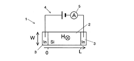
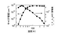
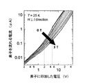
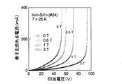
- the figure which shows the structural example of a magnetoresistive element The figure which shows the relationship between the electron density and mobility of a magnetoresistive element using an impurity silicon substrate, and temperature. The figure which shows the relationship between the applied voltage when the magnetic field of 0-3T is applied to the magnetoresistive element using an impurity silicon substrate at 25K, and an electric current. The figure which shows the relationship between the applied voltage and the magnetoresistive ratio (MR ratio) in the temperature 25K of the magnetoresistive element using an impurity silicon substrate. The figure which shows the relationship between the magnetoresistive effect and electron density when changing the temperature of the magnetoresistive element using an impurity silicon substrate.
- MR ratio magnetoresistive ratio
- the figure which shows the relationship between the applied voltage and electric current when a magnetic field of 0-3T is applied at room temperature of the magnetoresistive element using a high purity silicon The figure which shows the relationship between the applied voltage and magnetoresistive ratio (MR ratio) of the magnetoresistive element using the high purity silicon in room temperature (300K).
- FIG. 11 is a diagram showing a magnetoresistance ratio when a magnetic field of 0 to 9 T and a voltage of 20 V are applied to the magnetoresistive element of FIG. 10 at a temperature of 25K.
- FIG. 1 shows a schematic diagram of a magnetoresistive element made of an impurity silicon substrate used for measurement
- FIG. 2 shows a relationship between temperature and electron density and mobility of the magnetoresistive element used for measurement.
- the magnetoresistive element 1 includes a rectangular plate-like silicon substrate 2 and a pair of indium (In) electrodes 3 and 3 disposed on the upper surface thereof at a certain distance.
- a bias voltage having a predetermined value is applied between the indium electrodes 3 and 3 by the voltage application circuit 4.
- the current flowing through the silicon substrate 2 is measured by an ammeter 5.
- the ammeter 5 is provided in the voltage application circuit 4.
- the magnetoresistive element 1 the resistance value of the silicon substrate 2 is obtained from the voltage value applied between the electrodes 3 and 3 and the measured value of the ammeter 5. Therefore, the voltage application circuit 4 and the ammeter 5 function as a resistance detection circuit.
- the magnetoresistive element 1 was formed by processing the silicon substrate 2 having a size of 5 mm ⁇ 5 mm and a thickness of 525 ⁇ m.
- the width W of the electrode 3 was set to 0.3 mm, and the distance L between the electrodes 3 and 3 was set to 0.8 mm.
- FIG. 3 is a diagram showing the relationship between the voltage applied to the magnetoresistive element 1 and the current flowing through the magnetoresistive element 1 when a magnetic field of 0 to 3 T is applied to the magnetoresistive element 1 at a temperature of 25K. It can be seen from FIG. 3 that the more the magnetic field is applied, the less the current flows, that is, the magnetoresistance value of the magnetoresistive element 1 increases.
- FIG. 4 shows changes in magnetic field strength (T) and magnetoresistance ratio (MR ratio) when the applied voltage of the magnetoresistive element 1 at 25 K is used as a parameter
- FIG. 5 shows the change in temperature.
- the relationship between magnetic resistance (k ⁇ ) and carrier density (cm ⁇ 3 ) is shown.
- the MR ratio is defined by the following equation, where R is a resistance value in a non-magnetic field and ⁇ R is an increase in resistance value in a magnetic field with respect to the resistance R in a non-magnetic field.
- MR ratio ⁇ R / R
- FIG. 4 shows that the magnetoresistance ratio increases when the applied voltage is larger than when the applied voltage is small. From this, it is presumed that the magnetoresistance ratio increased due to the space charge effect seen when a high voltage was applied. Further, it can be seen from FIG. 5 that the magnetoresistive effect is observed at a low temperature of 40K or less. Since the electron density decreases as the temperature decreases, it is considered that the magnetoresistive effect has increased due to the decrease in electron density. From the above results, the present inventor predicted that the magnetoresistive effect would occur at a higher temperature in a high-purity semiconductor with a low electron density, and performed the following measurement.
- magnetoresistive element 1A a magnetoresistive element using a high-purity silicon substrate is referred to as “magnetoresistive element 1A”.
- FIG. 6 is a diagram showing the relationship between the voltage applied to the magnetoresistive element 1A and the current flowing through the magnetoresistive element 1A when a magnetic field of 0 to 3T is applied to the magnetoresistive element 1A at room temperature (300K).
- FIG. 7 is a diagram showing a change in magnetic field strength T and magnetoresistance ratio (MR ratio) when the applied voltage of the magnetoresistive element 1A at room temperature (300K) is used as a parameter. 6 and 7 that the magnetoresistive element 1A has a large magnetoresistive effect when a high voltage (100 V to 200 V) is applied at room temperature.
- MR ratio magnetoresistance ratio
- 8 and 9 are diagrams in which breakdown of the magnetoresistive effect seen in the magnetoresistive element 1A at temperatures of 25K and 300K was examined.
- 8 and 9 show the relationship between the applied voltage of the magnetoresistive element 1A and the current flowing through the magnetoresistive element 1 when a magnetic field of 0 to 3T is applied. 8 and 9 that the breakdown in the strong electric field is suppressed under the magnetic field.
- a huge magnetoresistance effect was observed near the breakdown, and the magnetoresistance increase rate in a magnetic field of 0 to 3 T exceeded 10000% at 25K and 1000% at room temperature (300K).
- a voltage at which such a giant magnetoresistance effect is seen is referred to as a “magnetoresistance voltage”.
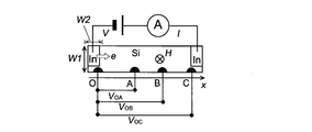
- FIG. 10 four voltage probes (O, A, B, C) are arranged between the electrodes of the magnetoresistive element 1A, and the distance between the voltage probe O and the voltage probes A, B, C is determined.
- the relationship with the magnetoresistance ratio was investigated.
- the voltage probe applies a voltage between the electrodes of the magnetoresistive element 1A and takes out a change in magnetoresistance when the magnetic field is changed as a voltage signal. Therefore, in the magnetoresistive element 1A shown in FIG. 10, a circuit that outputs a voltage between the voltage probe O and the voltage probes A, B, and C and an ammeter constitute a resistance detection circuit.
- the width W1 of the silicon substrate of the magnetoresistive element 1A used for the measurement was 2.8 mm, and the width W2 of the electrode was 0.3 mm or less.
- the distances between the voltage probe O and the voltage probes A, B, and C were set to 1.8 mm, 3.1 mm, and 4.5 mm, respectively.
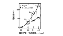
- FIG. 11 shows the relationship between the distance between the voltage probes and the potential difference between the voltage probes when a current of 0.1 ⁇ A and 40 ⁇ A flows through the magnetoresistive element 1A at a temperature of 25K and no magnetic field.
- a current of 0.1 ⁇ A flows, Ohm's law is followed, and the potential difference at this time is proportional to the distance x between the voltage probes.
- Mott-Gurney law Mott-Gurney law is followed, and the potential difference at this time is proportional to the 3/2 power of the distance between the voltage probes (x 3/2 where x is the distance between the voltage probes).
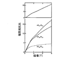
- FIG. 12 shows the magnetoresistance ratio when a magnetic field of 0 to 9 T and a voltage of 20 V are applied to the magnetoresistive element 1A at a temperature of 25K.
- the upper diagram in FIG. 12 shows the magnetoresistance ratio of the magnetoresistive element 1A (the entire silicon substrate), and the lower diagram shows the magnetoresistance ratio between the voltage probe O and the voltage probes A, B, and C.
- FIG. 12 shows that the magnetoresistance ratio increases as the distance between the voltage probes increases. There was no constant relationship between the distance between the voltage probes and the magnetoresistance ratio. Since the magnetoresistive effect is caused by the non-uniformity of the electron concentration and the electric field in the magnetic field, it is considered that the magnitude of the magnetoresistance varies depending on the position of the voltage probe.
- a magnetoresistive element using a high-purity silicon substrate shows a large magnetoresistive effect at room temperature (300 K). It is done. Increasing the distance between the pair of voltage probes arranged in the magnetoresistive element increases the applied voltage between the probes. Therefore, the sensitivity can be changed by changing the applied voltage or changing the distance between the voltage probes in accordance with the application of the magnetoresistive element (rotary encoder, linear encoder, magnetic head, etc.).
- the large magnetoresistive effect described above can be obtained not only with Si but also with a magnetoresistive element made of a high-purity semiconductor substrate such as GaAs, InP, AlAs, Cd Te, InAs, Ge, SiC, GaN, SiGe, ZnO, and InS. Can do.
- a magnetoresistive element made of a high-purity semiconductor substrate such as GaAs, InP, AlAs, Cd Te, InAs, Ge, SiC, GaN, SiGe, ZnO, and InS. Can do.
- an ohmic electrode such as Au or Al can be used as the electrode.
- the semiconductor substrate material and the electrode material may be appropriately selected in consideration of the compatibility between them. Further, the size of the semiconductor substrate and electrodes, and the distance between the electrodes can be set as appropriate according to the application.
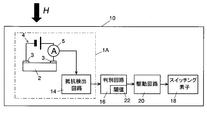
- FIG. 13 shows a specific embodiment of a magnetically sensitive switch using the magnetoresistive element of the present invention.
- the magnetic sensitive switch 10 includes the magnetoresistive element 1A described above, a resistance detection circuit 14 for obtaining a resistance value of the silicon substrate 2 based on a current measurement value of the ammeter 5, and an output value of the resistance detection circuit 14 set in advance.
- a discrimination circuit 16 that compares the threshold 22 and a drive circuit 20 that drives the switching element 18 based on the discrimination result of the discrimination circuit 16 are provided.
Landscapes
- Hall/Mr Elements (AREA)
- Switches That Are Operated By Magnetic Or Electric Fields (AREA)
Abstract
本発明の半導体磁気抵抗素子は、半導体基板としてのシリコン基板2と、その上に一定間隔をおいて配置された一対の電極3と、前記電極3,3間にバイアス電圧を印加する電圧印加回路4とを備えている。本発明では、300ケルビンにおけるキャリア密度が1013cm-3未満のシリコンを用いてシリコン基板2を構成したため、室温でも10倍を超える正の磁気抵抗効果を示す。
Description
本発明は、磁場を検知する磁気抵抗素子及び磁気感応スイッチに関する。
磁気抵抗(Magneto-Resistance:MR)効果とは、物質の電気抵抗が磁場中で変化する現象をいう。磁気抵抗素子は、歯車の回転速度を検出するセンサやハードディスク読み取り装置等に利用されている。近年では半導体材料を用いた磁気抵抗素子が提供されており、その利用は様々な分野で広がっている。
しかし、従来の半導体磁気抵抗素子はキャリア密度が1015cm-3程度の不純物半導体材料が用いられており(特許文献1参照)、キャリア密度が非常に低い高純度半導体は磁気抵抗素子には適さないと考えられていた。
しかし、従来の半導体磁気抵抗素子はキャリア密度が1015cm-3程度の不純物半導体材料が用いられており(特許文献1参照)、キャリア密度が非常に低い高純度半導体は磁気抵抗素子には適さないと考えられていた。
しかし、パワー半導体の分野では高電圧で使用されるため、耐圧性の高い、キャリア密度の少ない高純度半導体が多く用いられる。このような分野においても利用可能な磁気抵抗素子の開発が望まれていた。
本発明が解決しようとする課題は、キャリア密度が非常に低い半導体を用いた半導体磁気抵抗素子及び磁気感応スイッチを提供することである。
本発明が解決しようとする課題は、キャリア密度が非常に低い半導体を用いた半導体磁気抵抗素子及び磁気感応スイッチを提供することである。
本発明者らは、2つの金属接点に挟まれた、キャリア密度が非常に低い(300Kにおいて1013cm-3未満)高純度半導体からなる磁気抵抗素子が、0~3Tの磁場において、室温(300K)で1000%、25Kで10000%を超える大きな磁気抵抗を示すことを発見した。また、キャリア密度が1013cm-3未満の高純度半導体では、3~9Tの磁場に対して磁気抵抗は線形の依存性を示す。
本発明者らは、この現象は高純度半導体に強い電場を印加した時に生じる空間電荷効果がもたらす準中性の破れによって説明できると考えた。空間電荷効果とは、自由に動ける電子が少ない物質に大量の電子が注入された場合に内部に一様でない電場が生じ、電子が互いにクーロン斥力を及ぼしあって該物質が導電性を有するようになる現象のことを指す。不純物元素を添加した半導体に比べると高純度半導体は自由に動ける電子が非常に少ないため、大きな電圧を印加すると高純度半導体中の電子は空間電荷効果に支配される。
空間電荷効果が強い領域では準中性が破れ、電子同士がクーロン斥力を及ぼしあいながら運動するため、磁場中ではそれら電子の軌道が曲げられ、その結果、電子濃度と電場が不均一になり、大きな磁気抵抗効果が誘起される。
本発明に係る半導体磁気抵抗素子は、このような研究の成果に基づき成されたもので、
300K(ケルビン)におけるキャリア密度が1013cm-3未満の半導体基板と、
前記半導体基板に設けられた一対の電極と、
前記電極間にバイアス電圧を印加する電圧印加回路とを備えることを特徴とする。
300K(ケルビン)におけるキャリア密度が1013cm-3未満の半導体基板と、
前記半導体基板に設けられた一対の電極と、
前記電極間にバイアス電圧を印加する電圧印加回路とを備えることを特徴とする。
本発明の半導体磁気抵抗素子の磁気抵抗効果はバイアス電圧に依存する。従って、前記電圧印加回路が前記電極間に印加するバイアス電圧を制御する制御回路を設けることにより、半導体磁気抵抗素子の用途に応じた適宜の磁気抵抗効果を得ることができる。
この場合、前記バイアス電圧は、所定の磁気抵抗電圧であると良い。なお、「磁気抵抗電圧」とは、巨大な磁気抵抗効果が見られる電圧のことをいう。
この場合、前記バイアス電圧は、所定の磁気抵抗電圧であると良い。なお、「磁気抵抗電圧」とは、巨大な磁気抵抗効果が見られる電圧のことをいう。
また、本発明の半導体磁気抵抗素子は、半導体基板の抵抗値を検出する抵抗検出回路を有すると良い。
前記半導体基板は、Si、GaAs、InP、AlAs、CdTe、InAs、Ge、SiC、GaN、SiGe、ZnO、InSのいずれか一種であると良い。また、電極にはIn、Au、Al等のオーミック電極を用いることができる。特に、前記半導体基板をSiとし、前記電極をInにすると、半導体基板と電極とを整合性良く接合することができる。
また、本発明に係る磁気感応スイッチは、300K(ケルビン)におけるキャリア密度が1013cm-3未満の半導体基板と、前記半導体基板上に一定間隔をおいて配置された一対の電極と、前記電極間にバイアス電圧を印加する電圧印加回路と、前記半導体基板の抵抗値を検出する抵抗検出回路とを有する磁気抵抗素子と、
前記抵抗検出回路が検出する抵抗値と閾値との比較結果に基づきスイッチング動作を行うスイッチング素子とを備えることを特徴とする。
前記抵抗検出回路が検出する抵抗値と閾値との比較結果に基づきスイッチング動作を行うスイッチング素子とを備えることを特徴とする。
本発明の半導体磁気抵抗素子によれば、室温でも10倍を超える大きな磁気抵抗効果を得ることができる。
また、本発明の磁気感応スイッチによれば、半導体基板に磁気抵抗素子を設けることができるため、磁気感応スイッチ全体の構成を小型化することができる。
また、本発明の磁気感応スイッチによれば、半導体基板に磁気抵抗素子を設けることができるため、磁気感応スイッチ全体の構成を小型化することができる。
以下、図面を参照して本発明の磁気抵抗素子について説明する。
まず、室温(300K)における電子密度が1015cm-3程度のシリコン基板(以下、不純物シリコン基板という)から成る磁気抵抗素子を用いて磁気抵抗効果に関する測定を行った結果について説明する。図1は、測定に用いた不純物シリコン基板から成る磁気抵抗素子の概略図を示し、図2は温度と測定に用いた磁気抵抗素子の電子密度及び移動度との関係を示す。図1に示すように、前記磁気抵抗素子1は矩形板状のシリコン基板2とその上面に一定の距離をおいて配置された一対のインジウム(In)電極3,3から成る。インジウム電極3,3間には電圧印加回路4によって所定値のバイアス電圧が印加される。また、シリコン基板2に流れる電流は電流計5で測定される。ここでは電流計5は電圧印加回路4に設けられている。前記磁気抵抗素子1では、電極3,3間に印加される電圧値と電流計5の測定値とからシリコン基板2の抵抗値が求められる。従って、電圧印加回路4及び電流計5が抵抗検出回路として機能する。
なお、ここでは5mm×5mm、厚さ525μmのシリコン基板2を加工して磁気抵抗素子1を作成した。また、電極3の幅Wを0.3mmに、電極3,3間の距離Lを0.8mmに設定した。
まず、室温(300K)における電子密度が1015cm-3程度のシリコン基板(以下、不純物シリコン基板という)から成る磁気抵抗素子を用いて磁気抵抗効果に関する測定を行った結果について説明する。図1は、測定に用いた不純物シリコン基板から成る磁気抵抗素子の概略図を示し、図2は温度と測定に用いた磁気抵抗素子の電子密度及び移動度との関係を示す。図1に示すように、前記磁気抵抗素子1は矩形板状のシリコン基板2とその上面に一定の距離をおいて配置された一対のインジウム(In)電極3,3から成る。インジウム電極3,3間には電圧印加回路4によって所定値のバイアス電圧が印加される。また、シリコン基板2に流れる電流は電流計5で測定される。ここでは電流計5は電圧印加回路4に設けられている。前記磁気抵抗素子1では、電極3,3間に印加される電圧値と電流計5の測定値とからシリコン基板2の抵抗値が求められる。従って、電圧印加回路4及び電流計5が抵抗検出回路として機能する。
なお、ここでは5mm×5mm、厚さ525μmのシリコン基板2を加工して磁気抵抗素子1を作成した。また、電極3の幅Wを0.3mmに、電極3,3間の距離Lを0.8mmに設定した。
以下の測定は、5K~300Kの温度領域で、シリコン基板2の面直方向(シリコン基板2に電流が流れる方向に垂直な方向)に-9~9Tの磁場を印加して行った。
図3は、温度25Kにおいて磁気抵抗素子1に0~3Tの磁場を印加したときの当該磁気抵抗素子1に印加した電圧と前記磁気抵抗素子1を流れる電流との関係を示す図である。図3から、強い磁場を印加するほど電流が流れ難いことが、つまり磁気抵抗素子1の磁気抵抗値が大きくなることがわかる。
また、印加電圧が2V以下のときはオームの法則に従い電流は電圧に比例するが、印加電圧が5V以上では電流は電圧の二乗に比例した。つまり、高電圧では、電流と電圧との関係式は以下の空間電荷効果(モット・ガーネーの法則)に従い、電流密度をJ、電圧をV、誘電率をε、電子移動度をμとすると、Jは次のように表すことができる。

図3は、温度25Kにおいて磁気抵抗素子1に0~3Tの磁場を印加したときの当該磁気抵抗素子1に印加した電圧と前記磁気抵抗素子1を流れる電流との関係を示す図である。図3から、強い磁場を印加するほど電流が流れ難いことが、つまり磁気抵抗素子1の磁気抵抗値が大きくなることがわかる。
また、印加電圧が2V以下のときはオームの法則に従い電流は電圧に比例するが、印加電圧が5V以上では電流は電圧の二乗に比例した。つまり、高電圧では、電流と電圧との関係式は以下の空間電荷効果(モット・ガーネーの法則)に従い、電流密度をJ、電圧をV、誘電率をε、電子移動度をμとすると、Jは次のように表すことができる。
図4は、25Kにおける磁気抵抗素子1の印加電圧をパラメータとしたときの磁場強度(T)と磁気抵抗比(MR比)の変化の様子を示し、図5は、温度を変化させたときの磁気抵抗(kΩ)とキャリア密度(cm-3)との関係を示す。
なお、無磁界中の抵抗値をR、無磁界中の抵抗Rに対する有磁界中の抵抗値の増加分をΔRとすると、MR比は次の式で定義される。
MR比=ΔR/R
なお、無磁界中の抵抗値をR、無磁界中の抵抗Rに対する有磁界中の抵抗値の増加分をΔRとすると、MR比は次の式で定義される。
MR比=ΔR/R
図4から、印加電圧が大きい方が小さいときよりも磁気抵抗比が増大することが分かる。このことから、高電圧印加時にみられる空間電荷効果によって磁気抵抗比が増大したと推測される。また、図5から、40K以下の低温時において磁気抵抗効果がみられることが分かる。温度が低下するにつれて電子密度が減少することから、電子密度が減少したことにより磁気抵抗効果が増大したと考えられる。以上の結果から、本発明者は、電子密度が小さい高純度半導体では、もっと高い温度でも磁気抵抗効果が起こると予想し、次の測定を行った。
即ち、上述の磁気抵抗素子1のシリコン基板として、室温(300K)におけるキャリア密度が1.8×1012cm-3の高純度シリコン基板を用いた。その他の構成は前記磁気抵抗素子1と同じである。磁気抵抗素子1と区別するため、以下の説明では、高純度シリコン基板を用いた磁気抵抗素子を「磁気抵抗素子1A」と呼ぶ。
即ち、上述の磁気抵抗素子1のシリコン基板として、室温(300K)におけるキャリア密度が1.8×1012cm-3の高純度シリコン基板を用いた。その他の構成は前記磁気抵抗素子1と同じである。磁気抵抗素子1と区別するため、以下の説明では、高純度シリコン基板を用いた磁気抵抗素子を「磁気抵抗素子1A」と呼ぶ。
図6は、室温(300K)において磁気抵抗素子1Aに0~3Tの磁場を印加したときの当該磁気抵抗素子1Aに印加した電圧と前記磁気抵抗素子1Aを流れる電流との関係を示す図である。図7は、室温(300K)における磁気抵抗素子1Aの印加電圧をパラメータとしたときの磁場強度Tと磁気抵抗比(MR比)の変化の様子を示す図である。図6及び図7から、磁気抵抗素子1Aでは、室温において高電圧(100V~200V)を印加すると大きな磁気抵抗効果が起こることが分かる。
図8及び図9は、温度25K及び300Kにおける、磁気抵抗素子1Aにみられる磁気抵抗効果のブレークダウンについて調べた図である。図8及び図9は、いずれも0~3Tの磁場を印加したときの磁気抵抗素子1Aの印加電圧と前記磁気抵抗素子1を流れる電流との関係を示す。図8及び図9から、強電場におけるブレークダウンは磁場下で抑制されることが分かる。ブレークダウン近傍で巨大な磁気抵抗効果が見られ、0~3Tの磁場における磁気抵抗増大率は、25Kでは10000%、室温(300K)では1000%を超えた。このような巨大な磁気抵抗効果が見られる電圧を、本発明では「磁気抵抗電圧」と称することとする。
次に、図10に示すように磁気抵抗素子1Aの電極間に4個の電圧プローブ(O,A,B,C)を配置し、電圧プローブOと電圧プローブA,B,C間の距離と磁気抵抗比との関係について調べた。電圧プローブは、磁気抵抗素子1Aの電極間に電圧を印加し、磁界を変化させたときの磁気抵抗の変化を電圧信号として取り出すためのものである。従って、図10に示す磁気抵抗素子1Aでは、電圧プローブOと電圧プローブA,B,Cとの間の電圧を出力する回路と電流計とが抵抗検出回路を構成する。なお、測定に用いた磁気抵抗素子1Aのシリコン基板の幅W1は2.8mm、電極の幅W2は0.3mm以下とした。また、電圧プローブOと電圧プローブA,B,Cの間の距離はそれぞれ1.8mm,3.1mm、4.5mmに設定した。
図11は、温度25K、無磁場中において、磁気抵抗素子1Aに0.1μA、40μAの電流が流れているときの各電圧プローブ間の距離と各電圧プローブ間の電位差との関係を示す。0.1μAの電流が流れているときはオームの法則に従い、このときの電位差は電圧プローブ間の距離xに比例する。一方、40μAの電流が流れているときはモット・ガーネーの法則に従い、このときの電位差は電圧プローブ間の距離の3/2乗(電圧プローブ間の距離をxとするとx3/2)に比例する。
図12は、温度25Kにおいて、磁気抵抗素子1Aに対して0~9Tの磁場及び20Vの電圧を印加したときの磁気抵抗比を示す。図12の上図は磁気抵抗素子1A(シリコン基板全体)の磁気抵抗比を、下図は電圧プローブOと電圧プローブA,B,C間の磁気抵抗比を示す。図12から、電圧プローブ間の距離が大きいほど磁気抵抗比が増大することが分かる。なお、電圧プローブ間の距離と磁気抵抗比には一定の関係はみられなかった。磁気抵抗効果が磁場中における電子濃度や電場の不均一性に起因することから、電圧プローブの位置によって磁気抵抗の大きさに差が生じたものと思われる。
以上の結果から、高純度シリコン基板を用いた磁気抵抗素子では、室温(300K)において大きな磁気抵抗効果が見られ、特に印加電圧を大きくして空間電荷効果がみられると大きな磁気抵抗効果が得られる。磁気抵抗素子に配置する一対の電圧プローブ間の距離を大きくするとプローブ間の印加電圧が大きくなる。従って、磁気抵抗素子の用途(ロータリエンコーダ、リニアエンコーダ、磁気ヘッド等)に応じて、印加電圧を変えたり電圧プローブ間の距離を変更したりすることにより感度を変えることができる。
なお、上記した大きな磁気抵抗効果は、Siに限らずGaAs、InP、AlAs、Cd Te、InAs、Ge、SiC、GaN、SiGe、ZnO、InS等の高純度半導体基板から成る磁気抵抗素子で得ることができる。また、電極にはInの他、AuやAl等のオーミック電極を用いることができる。半導体基板材料及び電極材料は両者の相性を考慮して適宜選択するとよい。さらに、半導体基板や電極のサイズ、電極間の距離についても用途に応じて適宜設定することが可能である。
図13は本発明の磁気抵抗素子を用いた磁気感応スイッチの具体的な実施例を示す。
磁気感応スイッチ10は、上述の磁気抵抗素子1Aと、電流計5の電流測定値に基づいてシリコン基板2の抵抗値を求める抵抗検出回路14、この抵抗検出回路14の出力値と予め設定された閾値22とを比較する判別回路16、判別回路16の判別結果に基づきスイッチング素子18を駆動する駆動回路20を備えている。
磁気感応スイッチ10は、上述の磁気抵抗素子1Aと、電流計5の電流測定値に基づいてシリコン基板2の抵抗値を求める抵抗検出回路14、この抵抗検出回路14の出力値と予め設定された閾値22とを比較する判別回路16、判別回路16の判別結果に基づきスイッチング素子18を駆動する駆動回路20を備えている。
1、1A…磁気抵抗素子
2…シリコン基板
3…電極
4…電圧印加回路
5…電流計
10…磁気感応スイッチ
14…抵抗検出回路
16…判別回路
18…スイッチング素子
20…駆動回路
22…閾値
2…シリコン基板
3…電極
4…電圧印加回路
5…電流計
10…磁気感応スイッチ
14…抵抗検出回路
16…判別回路
18…スイッチング素子
20…駆動回路
22…閾値
Claims (7)
- 300ケルビンにおけるキャリア密度が1013cm-3未満の半導体基板と、
前記半導体基板上に一定間隔をおいて配置された一対の電極と、
前記電極間にバイアス電圧を印加する電圧印加回路とを備えることを特徴とする磁気抵抗素子。 - 前記半導体基板の抵抗値を検出する抵抗検出回路を備えることを特徴とする請求項1に記載の半導体磁気抵抗素子。
- 前記電圧印加回路が前記電極間に印加するバイアス電圧を制御する制御回路を備えることを特徴とする請求項1又は2に記載の半導体磁気抵抗素子。
- 前記半導体基板が、Si、GaAs、InP、AlAs、CdTe、InAs、Ge、SiC、GaN、SiGe、ZnO、InSのいずれか一種であることを特徴とする請求項1~3のいずれかに記載の半導体磁気抵抗素子。
- 前記半導体基板がSiであり、前記電極がInであることを特徴とする請求項4に記載の半導体磁気抵抗素子。
- 前記電圧印加回路により印加されるバイアス電圧が、所定の磁気抵抗電圧であることを特徴とする請求項1~5のいずれかに記載の半導体磁気抵抗素子。
- 300ケルビンにおけるキャリア密度が1013cm-3未満の半導体基板と、前記半導体基板上に一定間隔をおいて配置された一対の電極と、前記電極間にバイアス電圧を印加する電圧印加回路と、前記半導体基板の抵抗値を検出する抵抗検出回路とを有する磁気抵抗素子と、
前記抵抗検出回路が検出する抵抗値と閾値との比較結果に基づきスイッチング動作を行うスイッチング素子とを備えることを特徴とする磁気感応スイッチ。
Priority Applications (1)
| Application Number | Priority Date | Filing Date | Title |
|---|---|---|---|
| JP2011518325A JPWO2010140396A1 (ja) | 2009-06-05 | 2010-02-18 | 磁気抵抗素子及び磁気感応スイッチ |
Applications Claiming Priority (2)
| Application Number | Priority Date | Filing Date | Title |
|---|---|---|---|
| JP2009-136275 | 2009-06-05 | ||
| JP2009136275 | 2009-06-05 |
Publications (1)
| Publication Number | Publication Date |
|---|---|
| WO2010140396A1 true WO2010140396A1 (ja) | 2010-12-09 |
Family
ID=43297538
Family Applications (1)
| Application Number | Title | Priority Date | Filing Date |
|---|---|---|---|
| PCT/JP2010/052409 Ceased WO2010140396A1 (ja) | 2009-06-05 | 2010-02-18 | 磁気抵抗素子及び磁気感応スイッチ |
Country Status (2)
| Country | Link |
|---|---|
| JP (1) | JPWO2010140396A1 (ja) |
| WO (1) | WO2010140396A1 (ja) |
Cited By (2)
| Publication number | Priority date | Publication date | Assignee | Title |
|---|---|---|---|---|
| WO2016042871A1 (ja) * | 2014-09-17 | 2016-03-24 | 株式会社 東芝 | 磁場センサ |
| JP2017037030A (ja) * | 2015-08-12 | 2017-02-16 | 日本電信電話株式会社 | 半導体装置およびその製造方法 |
Citations (1)
| Publication number | Priority date | Publication date | Assignee | Title |
|---|---|---|---|---|
| JPH11312447A (ja) * | 1998-04-30 | 1999-11-09 | Murata Mfg Co Ltd | 近接センサ |
-
2010
- 2010-02-18 WO PCT/JP2010/052409 patent/WO2010140396A1/ja not_active Ceased
- 2010-02-18 JP JP2011518325A patent/JPWO2010140396A1/ja active Pending
Patent Citations (1)
| Publication number | Priority date | Publication date | Assignee | Title |
|---|---|---|---|---|
| JPH11312447A (ja) * | 1998-04-30 | 1999-11-09 | Murata Mfg Co Ltd | 近接センサ |
Non-Patent Citations (1)
| Title |
|---|
| MICHAEL P. DELMO ET AL.: "Large positive magnetoresistive effect in silicon induced by the space-charge effect", NATURE, vol. 457, 26 February 2009 (2009-02-26), pages 1112 - 1115 * |
Cited By (3)
| Publication number | Priority date | Publication date | Assignee | Title |
|---|---|---|---|---|
| WO2016042871A1 (ja) * | 2014-09-17 | 2016-03-24 | 株式会社 東芝 | 磁場センサ |
| JP2016061626A (ja) * | 2014-09-17 | 2016-04-25 | 株式会社東芝 | 磁場センサ |
| JP2017037030A (ja) * | 2015-08-12 | 2017-02-16 | 日本電信電話株式会社 | 半導体装置およびその製造方法 |
Also Published As
| Publication number | Publication date |
|---|---|
| JPWO2010140396A1 (ja) | 2012-11-15 |
Similar Documents
| Publication | Publication Date | Title |
|---|---|---|
| Rüster et al. | Very Large Tunneling Anisotropic Magnetoresistance<? format?> of a (G a, M n) A s/G a A s/(G a, M n) A s Stack | |
| KR100789119B1 (ko) | 자장 센서 | |
| Cheng et al. | Anomalous Transport in Sketched Nanostructures at the LaAlO 3/SrTiO 3 Interface | |
| Kazakova et al. | Optimization of 2DEG InAs/GaSb Hall sensors for single particle detection | |
| CN113167841B (zh) | 利用反常霍尔效应的磁传感器和霍尔传感器以及霍尔传感器的制造方法 | |
| Zhou et al. | Extraordinary magnetoresistance in encapsulated monolayer graphene devices | |
| Novoselov et al. | Submicron probes for Hall magnetometry over the extended temperature range from helium to room temperature | |
| CN103454602B (zh) | 一种基于拓扑绝缘体的磁场测量计及其测量方法 | |
| Wang et al. | High-performance graphene-based electrostatic field sensor | |
| JP5119450B2 (ja) | 温度センサ | |
| WO2010140396A1 (ja) | 磁気抵抗素子及び磁気感応スイッチ | |
| Behet et al. | InAs/Al0. 2Ga0. 8Sb quantum well Hall effect sensors | |
| CN103956427B (zh) | 感测元件 | |
| Goswami et al. | Highly Enhanced Thermopower in Two-Dimensional Electron Systems<? format?> at Millikelvin Temperatures | |
| Naydenova et al. | Diffusion thermopower of (ga, mn) as/gaas tunnel junctions | |
| WO2019079270A1 (en) | MICRO HALL EFFECT DEVICES FOR SIMULTANEOUS CURRENT AND TEMPERATURE MEASUREMENTS FOR HIGH AND LOW TEMPERATURE ENVIRONMENTS | |
| Ishikura et al. | Electrical spin injection from ferromagnet into an InAs quantum well through a MgO tunnel barrier | |
| Han et al. | High Field Resolution Hall Sensor Based on AlSb/InAs 2DEG for Magnetic Particle Detection | |
| CN110515017B (zh) | 一种超高灵敏度磁场传感器 | |
| Luo et al. | Resistance transition assisted geometry enhanced magnetoresistance in semiconductors | |
| Sun et al. | A top-contacted extraordinary magnetoresistance sensor fabricated with an unpatterned semiconductor epilayer | |
| Kunets et al. | Doped-channel micro-Hall devices: Size and geometry effects | |
| Cronin et al. | Thermoelectric transport properties of single bismuth nanowires | |
| Devlikanova et al. | The Study of SOI Split-drain Field-effect Hall sensor In Partial Depletion Mode | |
| Xia et al. | AlGaN/GaN Split-Electrode Sectorial Sensor Array for Ultra-Low Magnetic Field Detection at 8 µT |
Legal Events
| Date | Code | Title | Description |
|---|---|---|---|
| 121 | Ep: the epo has been informed by wipo that ep was designated in this application |
Ref document number: 10783183 Country of ref document: EP Kind code of ref document: A1 |
|
| DPE1 | Request for preliminary examination filed after expiration of 19th month from priority date (pct application filed from 20040101) | ||
| WWE | Wipo information: entry into national phase |
Ref document number: 2011518325 Country of ref document: JP |
|
| NENP | Non-entry into the national phase |
Ref country code: DE |
|
| 122 | Ep: pct application non-entry in european phase |
Ref document number: 10783183 Country of ref document: EP Kind code of ref document: A1 |